

Page 1

PIC10F220/222
Data Sheet
6-Pin, 8-Bit Flash Microcontrollers
© 2005 Microchip Technology Inc. Preliminary DS41270A
Page 2

Note the following details of the code protection feature on Microchip devices:
• Microchip products meet the specification contained in their particular Microchip Data Sheet.
• Microchip believes that its family of products is one of the most secure families of its kind on the market today, when used in the
intended manner and under normal conditions.
• There are dishonest and possibly illegal methods used to breach the code protection feature. All of these methods, to our
knowledge, require using the Microchip products in a manner outside the operating specifications contained in Microchip’s Data
Sheets. Most likely, the person doing so is engaged in theft of intellectual property.
• Microchip is willing to work with the customer who is concerned about the integrity of their code.
• Neither Microchip nor any other semiconductor manufacturer can guarantee the security of their code. Code protection does not
mean that we are guaranteeing the product as “unbreakable.”
Code protection is constantly evolving. We at Microchip are committed to continuously improving the code protection features of our
products. Attempts to break Microchip’s code protection feature may be a violation of the Digit al Millennium Copyright Act. If suc h a c t s
allow unauthorized access to your software or other copyrighted work, you may have a right to sue for relief under that Act.
Information contained in this publication regarding device
applications and the like is provided only for your convenience
and may be superseded by updates. It is your responsibility to
ensure that your application meets with your specifications.
MICROCHIP MAKES NO REPRESENTATIONS OR WARRANTIES OF ANY KIND WHETHER EXPRESS OR IMPLIED,
WRITTEN OR ORAL, STATUTORY OR OTHERWISE,
RELATED TO THE INFORMATION, INCLUDING BUT NOT
LIMITED TO ITS CONDITION, QUALITY, PERFORMANCE,
MERCHANTABILITY OR FITNESS FOR PURPOSE.
Microchip disclaims all liability arising from this information and
its use. Use of M icrochip’s prod ucts as critical components in
life support systems is not authorized except with express
written approval by Microchip. No licenses are conveyed,
implicitly or otherwise, under any Microchip intellectual property
rights.
Trademarks
The Microchip name and logo, the Microchip logo, Accuron,
dsPIC, K
EELOQ, microID, MPLAB, PIC, PICmicro, PICSTART,
PRO MATE, PowerSmart, rfPIC, and SmartShunt are
registered trademarks of Microchip Technology Incorporated
in the U.S.A. and other countries.
AmpLab, FilterLab, Migratable Memory, MXDEV, MXLAB,
PICMASTER, SEEVAL, SmartSensor and The Embedded
Control Solutions Company are registered trademarks of
Microchip Technology Incorporated in the U.S.A.
Analog-for-the-Digital Age, Application Maestro, dsPICDEM,
dsPICDEM.net, dsPICworks, ECAN, ECONOMONITOR,
FanSense, FlexROM, fuzzyLAB, In-Circuit Serial
Programming, ICSP, ICEPIC, Linear Active Thermistor,
MPASM, MPLIB, MPLINK, MPSIM, PICkit, PICDEM,
PICDEM.net, PICLAB, PICtail, PowerCal, PowerInfo,
PowerMate, PowerTool, rfLAB, rfPICD EM, Select Mode,
Smart Serial, SmartTel, Total Endurance and WiperLock are
trademarks of Microchip Technology Incorporated in the
U.S.A. and other countries.
SQTP is a service mark of Microchip Technology Incorporated
in the U.S.A.
All other trademarks mentioned herein are property of their
respective companies.
© 2005, Microchip Technology Incorporated, Printed in the
U.S.A., All Rights Reserved.
Printed on recycled paper.
Microchip received ISO/TS-16949:2002 quality system certification for
its worldwide headquarters, design and wafer fabrication facilities in
Chandler and Tempe, Arizona and Mountain View, California in
October 2003. The Company’s quality system processes and
procedures are for its PICmicro
devices, Serial EEPROMs, microperipherals, nonvolatile memory and
analog products. In addition, Microchip’s quality system for the design
and manufacture of development systems is ISO 9001:2000 certified.
®
8-bit MCUs, KEELOQ
®
code hopping
DS41270A-page ii Preliminary © 2005 Microchip Technology Inc.
Page 3

PIC10F220/222
6-Pin, 8-Bit Flash Microcontrollers
Device Included In This Data Sheet
•PIC10F220
•PIC10F222
High-Performance RISC CPU
• Only 33 single-word instructions to learn
• All single-cycle instructions except for program
branches which are two-cycle
• 12-bit wide instructions
• 2-level deep hardware stack
• Direct, Indirect and Relative Addressing modes
for data and instructions
• 8-bit wide data path
• 8 special function hardware registers
• Operating speed:
- 500 ns instruction cycle with 8 MHz internal
clock
-1μs instruction cycle with 4 MHz internal
clock
Special Microcontroller Features
• 4 or 8 MHz precision internal oscillator:
- Factory calibrated to ±1%
• In-Circuit Serial Programming™ (ICSP™)
programming capability
• In-Circuit Debugging (ICD) support
• Power-on Reset (PO R)
• Short Device Reset Timer (DRT) – 1.125 ms
typical
• Watchdog Timer (WDT) with dedicated on-chip
RC oscillator for reliable operation
• Programmable code protection
• Multiplexed MCLR
• Internal weak pull-ups on I/O pins
• Power-saving Sleep mode
• Wake-up from Sleep on pin change
input pin
Low Power Features/CMOS Technology
• Operating Current:
- < 350 μA @ 2V, 4 MHz
• Standby Current:
- 100 nA @ 2V, typical
• Low-power, high-speed Flash technology:
- 100,000 Flash endurance
- > 40 year retention
• Fully static design
• Wide operating voltage range: 2.0V to 5.5V
• Wide temperature range:
- Industrial: -40°C to +85°C
- Extended: -40°C to +125°C
Peripheral Features
• 4 I/O pins:
- 3 I/O pins with individual direction control
- 1 input only pin
- High-current sink/source for direct LED drive
- Wake-up on change
- Weak pull-ups
• 8-bit real-time clock/counter (TMR0) with 8-bit
programmable prescaler
• Analog-to-Digital (A/D) Converter
- 8-bit resolution
- 2 external input channels
- 1 internal input channel dedicated to
conversion of the 0.6V absolute voltage
reference
Device
PIC10F220 256 16 4 1 2
PIC10F222 512 23 4 1 2
© 2005 Microchip Technology Inc. Preliminary DS41270A-page 3
Program Memory Data Memory
I/O
Flash (words) SRAM (bytes)
Timers
8-bit
8-Bit A/D (ch)
Page 4

PIC10F220/222
Pin Diagrams
6-Lead SOT -23
8-Lead PDIP
GP0/AN0/ICSPDAT
V
SS
GP1/AN1/ICSPCLK
N/C
VDD
GP2/T0CKI/F
GP1/AN1/ICSPCLK
OSC4
PIC10F220/222
PIC10F220/222
6
5
4
8
7
6
5
GP3/MCLR
VDD
GP2/T0CKI/FOSC4
GP3/MCLR/VPP
VSS
N/C
GP0/AN0/ICSPDAT
/VPP
1
2
3
1
2
3
4
DS41270A-page 4 Preliminary © 2005 Microchip Technology Inc.
Page 5

PIC10F220/222
Table of Contents
1.0 General Description............................................................................ ....... .... .. .... .. .... ...................................................................7
2.0 Device Varieties .......................................................................................................................................................................... 9
3.0 Architectural Overview ...............................................................................................................................................................11
4.0 Memory Organization................................................................................................................................................................. 15
5.0 I/O Port......................................... ..................... ..................... ..................... ............................................................................... 23
6.0 TMR0 Module and TMR0 Register............................................................................................................................................. 27
7.0 Analog-to-Digital (A/D) converter ............................................................................................................................................... 31
8.0 Special Feature s Of The CPU.......... .......................................... ..................... ..................... ...................................................... 35
9.0 Instruction Set Summary............................................................................................................................................................ 45
10.0 Electrical Characteristics............................................................................................................................................................ 53
11.0 Development Support.................................................................................................................................................................63
12.0 DC and AC Characteristics Graphs and Charts.........................................................................................................................67
13.0 Packaging Information. ..................... ..................... ..................... ..................... ........................................................................... 69
Index .................................................................................................................................................................................................... 73
The Microchip Web Site................................... ............................................................. ....................................................................... 75
Customer Change Notification Service ................................................................................................................................................ 75
Customer Support................................................................................................................................................................................ 75
Reader Response................................................................................................................................................................................76
Product Identification System .............................................................................................................................................................. 77
TO OUR VALUED CUSTOMERS
It is our intention to provide our valued customers with the best documentation possible to ensure successful use of your Microchip
products. To this end, we will continue to improve our publications to better suit your needs. Our publications will be refined and
enhanced as new volumes and updates are introduced.
If you have any questions or c omm ents regarding t his publication, p lease c ontact the M arket ing Co mmunications Department via
E-mail at docerrors@microchip.com or fax the Reader Response Form in the back of this data sheet to (480) 792-4150. We
welcome your feedback.
Most Current Data Sheet
To obtain the most up-to-date version of this data sheet, please register at our Worldwide Web site at:
http://www.microchip.com
You can determine the version of a data sheet by examining its literature number found on the bottom outside corner of any page.
The last character of the literature number is the version number, (e.g., DS30000A is version A of document DS30000).
Errata
An errata sheet, describing minor operational differences from the data sheet and recommended workarounds, may exist for current
devices. As device/documentation issues become known to us, we will publish an errata sheet. The errata will specify the revision
of silicon and revision of document to which it applies.
To determine if an errata sheet exists for a particular device, please check with one of the following:
• Microchip’s Worldwide Web site; http://www.microchip.com
• Your local Microchip sales office (see last page)
When contacting a sales office, please specify which device, revision of silicon and data sheet (include literature number) you are
using.
Customer Notification System
Register on our web site at www.microchip.com to receive the most current information on all of our products.
© 2005 Microchip Technology Inc. Preliminary DS41270A-page 5
Page 6

PIC10F220/222
NOTES:
DS41270A-page 6 Preliminary © 2005 Microchip Technology Inc.
Page 7

PIC10F220/222
1.0 GENERAL DESCRIPTION
The PIC10F220/222 devices, from Microchip
Technology, are low-cost, high-performan ce, 8-b it, fully
static, Flash-based CMOS microcontrollers. They
employ a RISC architecture with only 33 single-word,
single-cycle instructions. All instructions are singlecycle (1 μs @ 4 MHz) except for prog ram branches,
which take two cycles. The PIC10F220/222 devices
deliver performance in an order of magnitude higher
than their competitors in the same price category. The
12-bit wide instructions are highly symmetrical, resulting in a typ ical 2:1 co de compre ssion over o ther 8-bi t
microcontrollers in i ts class . The easy-to-us e and easyto-remember instr ucti on se t reduc es de velop ment time
significantly.
The PIC10F220/222 products are equipped with special features that reduce system cost and power
requirements. The Power-on Reset (POR) and Device
Reset Ti mer (DR T) e limin ates the ne ed fo r the externa l
Reset circuitry. Internal Oscillator (INTOSC) mode is
provided, thereby, preserving the li mi ted num be r of I/O
pins available. Power-saving Sleep mode, Watchdog
Timer and code protection features improve system
cost, power and reliability.
The PIC10F220/222 devices are available in costeffective Flash, which is suitable for production in any
volume. The customer can take full advantage of
Microchip’s price leadership in Flash programmable
microcontrollers while benefiting from the Flash
programmable flexibility.
The PIC10F220/222 products are supported by a fullfeatured macro assembler, a software simulator, an
in-circuit debugger, a C compiler, a low-cost
development programmer and a full featured programmer. All the tools are supported on IBM
compatible machines.
®
PC and
1.1 Applications
The PIC10F220/222 devices fit in applications ranging
from personal care app li anc es an d s ecu rity s yst ems to
low-power remote transmitters/receivers. The Flash
technology makes customizing application programs
(transmitter codes, appliance settings, receiver frequencies, etc.) extremely fast and convenient. The
small footprint packages, for through hole or surface
mounting, make th ese micr ocontroll ers wel l suited for
applications with space limitations. Low-cost, lowpower , high-perform ance, ease of use and I/O fl exibility
make the PIC10F220/222 devices very versatile, even
in areas where no m icrocontroller us e has been con sidered before (e.g., timer functions, logic and PLDs in
larger systems and coprocessor applications).
T ABLE 1-1: PIC10F220/222 DEVICES
Clock Maximum Frequency of Operation (MHz) 8 8
Memory Flash Program Memory 256 512
Data Memory (bytes) 16 23
Peripherals Timer Module(s) TMR0 TMR0
Wake-up from Sleep on Pin Change Yes Yes
Analog Inputs 2 2
Features I/O Pins 3 3
Input Only Pins 1 1
Internal Pull-ups Yes Yes
In-Circuit Serial Programming™ Yes Yes
Number of Instructions 33 33
Packages 6-pin SOT-23,
Note 1: The PIC10F220/222 devices have Power-on Reset, selectable Watchdog Timer, selectable code-protect, high I/O
current capability and precision internal oscillator.
2: The PIC10F220/222 devices use serial programming with data pin GP0 and clock pin GP1.
© 2005 Microchip Technology Inc. Preliminary DS41270A-page 7
(1, 2)
PIC10F220 PIC10F222
8-pin PDIP
6-pin SOT-23,
8-pin PDIP
Page 8

PIC10F220/222
NOTES:
DS41270A-page 8 Preliminary © 2005 Microchip Technology Inc.
Page 9

2.0 DEVICE VARIETIES
A variety of packaging options are available. Depending on application and production requirements, the
proper device option can be selected using the
information in th is section. Wh en placing orde rs, please
use the PIC10F220/222 Product Identification System
at the back of this data s heet to s pecify the correct p art
number.
2.1 Quick Turn Programming (QTP) Devices
Microchip offers a QTP programming service for
factory production orders. This service is made
available for users who choose not to program
medium-to-high quantity units and whose code
patterns have stabilized. The devices are identical to
the Flash devices but with all Flash locations and fuse
options already programmed by the factory. Certain
code and prototype verification procedures do apply
before production shipments are available. Please
contact your loc al Microchi p Technology sales office for
more details.
PIC10F220/222
2.2 Serialized Quick Turn
Programming
Microchip offers a unique programming service, where
a few user-defined locations in each device are
programmed with different serial numbers. The serial
numbers may be random, pseudo-random or
sequential.
Serial programming allows each device to have a
unique number, which can serve as an entry code,
password or ID number.
SM
(SQTPSM) Devices
© 2005 Microchip Technology Inc. Preliminary DS41270A-page 9
Page 10

PIC10F220/222
NOTES:
DS41270A-page 10 Preliminary © 2005 Microchip Technology Inc.
Page 11

PIC10F220/222
3.0 ARCHITECTURAL OVERVIEW
The high performance of the PIC10F220/222 devices
can be attributed to a number of architectural features
commonly found in RISC microprocessors. To begin
with, the PIC10F220/222 devices use a Harvard architecture in which program and data are accessed on
separate buses. This improves bandwidth over traditional von Neumann architectures where program and
data are fetch ed on the sa me bu s. Separating program
and data memor y further allow s instructions to be sized
differently than the 8-bit wide data word. Instruction
opcodes are 12 bit s wide, making it p ossible to have all
single-word instructions. A 12-bit wide program memory access bus fetches a 12-bit instruction in a single
cycle. A two-stage pipeline overlaps fetch and execution of instructions. Consequently, all instructions (33)
execute in a single cycle (1 μs @ 4 MHz or
500 ns @ 8 MHz) except for program branches.
The table belo w lists p rogram me mory (Flash) and data
memory (RAM) for the PIC10F220/222 devices.
Memory
Device
Program Data
PIC10F220 256 x 12 16 x 8
PIC10F222 512 x 12 23 x 8
The PIC10F220/222 devices contain an 8-bit ALU and
working register. The ALU is a general purpose arithmetic unit. It perfor ms arithmetic a nd Boolean fun ctions
between data in the working register and any register
file.
The ALU is 8 bits wide and capable of addition, subtraction, shift and logical operations. Unless otherwise
mentioned, arithmetic operations are two’s complement in nature. In two-operand instructions, one operand is typically the W (Working) register. The other
operand is either a file register or an immediate
constant. In sing le ope ran d inst ruction s, the operan d is
either the W register or a file register.
The W register is an 8-bit workin g register used for ALU
operations. It is not an addressable register.
Depending on the instruction executed, the ALU may
affect the values of the Carry (C), Digit Carry (DC) and
Zero (Z) bits in the ST ATUS register . The C and DC bits
operate as B
tively, in subtraction. See the SUBWF and ADDWF
instructions for examples.
A simplified block diagram is shown in Figure 3-1 with
the corresponding device pins described in Table 3-1.
orrow and Digit borrow out bits, respec-
The PIC10F220/222 devices can directly or indirectly
address its register files and data memory. All Special
Function Registers (SFR), including the Program
Counter (PC), are mapped in the data memory. The
PIC10F220/222 devices have a highly orthogonal
(symmetrica l) instruct ion set that m akes it possib le to
carry out any operation, on any register, using any
addressing mode. This symmetrical nature and lack of
“special optimal situ ations” make programm ing with the
PIC10F220/222 devices simple yet efficient. In
addition, the learning curve is reduced significantly.
© 2005 Microchip Technology Inc. Preliminary DS41270A-page 11
Page 12
PIC10F220/222
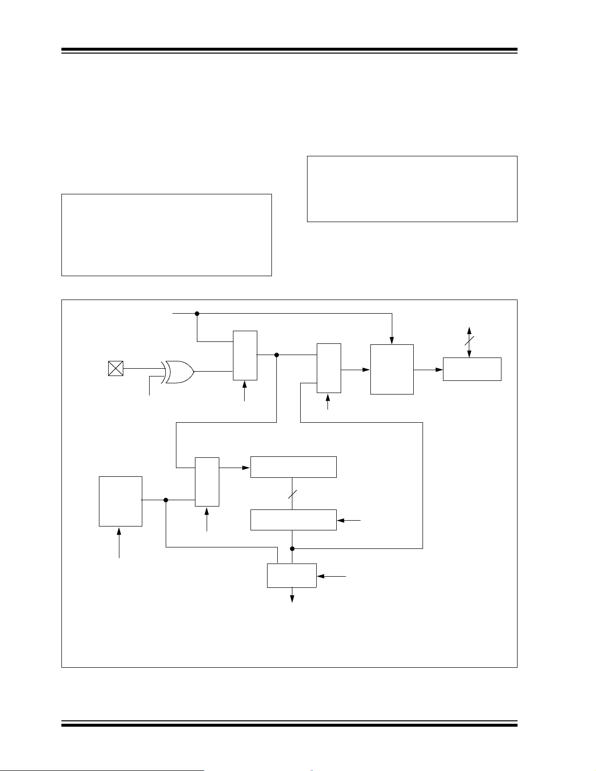
FIGURE 3-1: BLOCK DIAGRAM
9-10
Program Counter
STACK1
STACK2
Direct Addr
Program
Bus
Flash
512 x 12 or
256 x 12
Program
Memory
12
Instruction reg
RAM Addr
5
Data Bus
RAM
23 or 16
bytes
File
Registers
Addr MUX
5-7
FSR reg
9
Indirect
Addr
8
GPIO
GP0/AN0/ICSPDAT
GP1/AN1/ICSPCLK
GP2/T0CKI/FOSC4
GP3/MCLR/VPP
3
STATUS reg
ALU
W reg
Timer0
MUX
ADC
Absolute
Voltage
Reference
AN0
AN1
Instruction
Decode and
Control
Timing
Generation
8
MCLR
Device Reset
Timer
Power-on
Reset
Watchdog
Timer
Internal RC
Clock
VDD, VSS
8
TABLE 3-1: PINOUT DESCRIPTION
Name Function
Input
Type
GP0/AN0/ICSPDAT GP0 TTL CMOS Bidirectional I/O pin. Can be software programmed for internal weak
AN0 AN — Analog Input.
ICSPDAT ST CMOS In-Circuit Programming data.
GP1/AN1/ICSPCLK GP1 TTL CMOS Bidirectional I/O pin. Can be software programmed for internal weak
AN1 AN — Analog Input.
ICSPCLK ST CMOS In-Circuit Programming clock.
GP2/T0CKI/FOSC4 GP2 TTL CMOS Bidirectional I/O pin.
T0CKI ST — Clock input to TMR0.
OSC4 — CMOS Oscillator/4 output.
F
GP3/MCLR
/VPP GP3 TTL — Input pin. Can be software programmed for internal weak pull-up and
MCLR
PP HV — Programming voltage input.
V
DD VDD P — Positive supply for logic and I/O pins.
V
V
SS VSS P — Ground reference for logic and I/O pins.
Legend: I = Input, O = Output, I/O = Input/Output, P = Power, — = Not used, TTL = TTL input,
ST = Schmitt Trigger input, AN = Analog Input
Output
Type
Description
pull-up and wake-up from Sleep on pin change.
pull-up and wake-up from Sleep on pin change.
wake-up from Sleep on pin change.
ST — Master Clear (Reset). When configured as MC LR, this pin is an
active-low Reset to the device. Voltage on MCLR
exceed V
DD during normal device operation or the device will enter
/VPP must not
Programming mode. Weak pull-up is always on if configured as MCLR
.
DS41270A-page 12 Preliminary © 2005 Microchip Technology Inc.
Page 13
PIC10F220/222
3.1 Clocking Scheme/Instruction Cycle
The clock is internally divided by four to generate four
non-overlapping quadrature clocks, namely Q1, Q2,
Q3 and Q4. Internally, the PC is incremented every Q1,
and the instruction is fetched from program memory
and latched into the Instru ction Regis ter (IR) in Q4. It is
decoded and executed during Q1 through Q4. The
clocks and instruction execution flow is shown in
Figure 3-2 and Example 3-1.
FIGURE 3-2: CLOCK/INSTRUCTION CYCLE
Q2 Q3 Q4
OSC1
Q1
Q2
Q3
Q4
PC
Q1
PC
Q1
3.2 Instruction Flow/Pipelining
An instruction cycle consists of four Q cycles (Q1, Q2,
Q3 and Q4). The instruction fetch and execute are
pipelined such that fetch takes one instruction cycle,
while decode and execute takes another instruction
cycle. However, due to the pipelining, each instruction
effectively executes in one cycle. If an instruction
causes the PC to change (e.g ., GOTO), t hen two c yc le s
are required to complete the ins tructi on (Exampl e 3-1).
A fetch cycle begins with the PC incrementing in Q1.
In the execution cy cle, the fetch ed instruction i s latched
into the Instr uction Regist er in cycle Q1. Th is instruction is then decoded and executed during the Q2, Q3
and Q4 cycles. Data memory is read during Q2
(operand read) and written during Q4 (destination
write).
Q2 Q3 Q4
PC + 1 PC + 2
Q2 Q3 Q4
Q1
Internal
Phase
Clock
Fetch INST (PC)
Execute INST (PC - 1)
Fetch INST (PC + 1)
Execute INST (PC)
Fetch INST (PC + 2)
Execute INST (PC + 1)
EXAMPLE 3-1: INSTRUCTION PIPELINE FLOW
1. MOVLW 03H
2. MOVWF GPIO
3. CALL SUB_1
4. BSF GPIO, BIT1
All instructions are si ngle cycle, except for any program bra nches. These tak e two cycles, since th e fetch instruction
is “flushed” from the pipeline, while the new instruction is being fetched and then executed.
Fetch 1 Execute 1
Fetch 2 Execute 2
Fetch 3 Execute 3
Fetch 4 Flush
Fetch SUB_1 Execute SUB_1
© 2005 Microchip Technology Inc. Preliminary DS41270A-page 13
Page 14

PIC10F220/222
NOTES:
DS41270A-page 14 Preliminary © 2005 Microchip Technology Inc.
Page 15

PIC10F220/222
4.0 MEMORY ORGANIZATION
The PIC10F220/222 memories are organized into program memory and data memory. Data memory banks
are accessed using the File Select Register (FSR).
4.1 Program Memory Organization for the PIC10F220
The PIC10F220 devices hav e a 9-bit Prog ram Coun ter
(PC) capable of addressing a 512 x 12 program
memory space.
Only the first 256 x 12 (0000h-00FFh) for the
PIC10F220 are physically implemented (see
Figure 4-1). Accessing a location above these
boundaries will cause a wraparound within the first
256 x 12 space (PIC10F220). The effective Reset
vector is at 0000h, (see Figure 4-1). Location 00FF h
(PIC10F220) contains the internal clock oscillator
calibration value. This value should never be
overwritten.
FIGURE 4-1: PROGRAM MEMORY MAP
AND STACK FOR THE
PIC10F220
PC<7:0>
CALL, RETLW
Stack Level 1
Stack Level 2
<8:0>
9
4.2 Program Memory Organization for the PIC10F222
The PIC10F222 devices have a 10-bit Program
Counter (PC) capable of addressing a 1024 x 12
program memory space.
Only the first 512 x 12 (0000h-01FFh) for the MemHigh are physically implemented (see Figure 4-2).
Accessing a location above these boundaries will
cause a wraparound within the first 512 x 12 space
(PIC10F222). The effective Reset vector is at 0000h
(see Figure 4-2). Location 01FFh (PIC10F222) contains the internal clock oscillator calibration value.
This value should never be overwritt en.
FIGURE 4-2: PROGRAM MEMORY MAP
AND STACK FOR THE
PIC10F222
<9:0>
10
0000h
CALL, RETLW
PC<8:0>
Stack Level 1
Stack Level 2
Reset Vector
On-Chip Program
Memory
(1)
Reset Vector
On-chip Program
Memory
Space
User Memory
256 Word
Note 1: Address 0000h becomes the
effective Reset vector. Location 00FFh
contains the MOVLW xx internal oscillator
calibration value.
(1)
0000h
00FFh
0100h
01FFh
Space
User Memory
512 Words
Note 1: Address 0000h becomes the effective
Reset vector. Location 01FFh contains the
MOVLW xx internal oscillator calibration
value.
01FFh
0200h
02FFh
© 2005 Microchip Technology Inc. Preliminary DS41270A-page 15
Page 16

PIC10F220/222
4.3 Data Memory Organization
Data memory is composed of registers or bytes of
RAM. Therefore, d ata memory for a device is sp ec ifie d
by its register file. The register file is divided into two
functional groups: Special Function Registers (SFR)
and General Purpose Registers (GPR).
The Special Function Reg ist ers incl ude the TM R0 register, the Program Counter (PC), the STATUS register,
the I/O register (GPIO) and the File Select Register
(FSR). In addition, Speci al Function Registe rs are used
to control the I/O port configuration and prescaler
options.
The General Purpose Registers are used for data and
control information under com mand of the instructions .
For the PIC10F220, the register file is composed of
9 Special Function Registers and 16 General Purpose
Registers (Figure 4-3, Figure 4-4).
For the PIC10F222, the register file is composed of
9 Special Function Registers and 23 General Purpose
Registers (Figure 4-4).
4.3.1 GENERAL PURPOSE REGISTER
FILE
The General Purpos e Registe r file i s accessed , eithe r
directly o r indirectly, through the F ile Select Regist er
(FSR). See Section 4.9 “Indirect Data Addressing;
INDF and FSR Registers”.
FIGURE 4-4: PIC10F222 REGISTER
FILE MAP
File Address
(1)
00h
01h
02h
03h
04h
05h
06h
07h
08h
09h
1Fh
Note 1: Not a physical register. See Section 4.9
“Indirect Data Addressing; INDF and
FSR Registers”.
INDF
TMR0
PCL
STATUS
FSR
OSCCAL
GPIO
ADCON0
ADRES
General
Purpose
Registers
FIGURE 4-3: PIC10F220 REGIST E R
FILE MAP
File Address
(1)
00h
01h
02h
03h
04h
05h
06h
07h
08h
09h
0Fh
10h
1Fh
Note 1: Not a physical register. See Section 4.9
“Indirect Data Addressing; INDF and
FSR Registers”.
2: Unimplemented, read as 00h.
INDF
TMR0
PCL
STATUS
FSR
OSCCAL
GPIO
ADCON0
ADRES
Unimplemented
General
Purpose
Registers
(2)
DS41270A-page 16 Preliminary © 2005 Microchip Technology Inc.
Page 17

PIC10F220/222
4.3.2 SPECIAL FUNCTION REGISTERS
The Special Function Registers (SFRs) are registers
used by the CPU and per ipheral functio ns to con trol the
operation of the device (Table 4-1).
The Special Function Registers can be classified into
two sets. The Special Function Registers associated
with the “core” functions are described in this section.
Those related to the operation of the peripheral
features are described in the section for each
peripheral feature.
TABLE 4-1: SPECIAL FUNCTION REGISTER (SFR) SUMMARY
Address Name Bit 7 Bit 6 Bit 5 Bit 4 Bit 3 Bit 2 Bit 1 Bit 0
00h INDF Uses contents of FSR to address data memory (not a physical register) xxxx xxxx 22
01h TMR0 8-bit Real-Time Clock/Counter xxxx xxxx 27
02h PCL
03h STATUS GPWUF
04h FSR Indirect Data Memory Address Pointer 111x xxxx 22
05h OSCCAL CAL6 CAL5 CAL4 CAL3 CAL2 CAL1 CAL0 FOSC4 1111 1110 20
06h GPIO
07h ADCON0 ANS1 ANS0
08h ADRES Result of Analog-to-Digital Conversion xxxx xxxx 32
N/A TRISGPIO
N/A OPTION GPWU
Legend: — = unimplemented, read as ‘0’, x = unknown, u = unchanged.
Note 1: The upper byte of the Program Counter is not directly accessible. See S ecti on 4.7 “Program Counter” for an
(1)
Low-Order 8 bits of PC 1111 1111 21
— —TOPD ZDCC0--1 1xxx
— — — — GP3 GP2 GP1 GP0 ---- xxxx 23
— — CHS1 CHS0 GO/DONE ADON 11-- 1100 32
— — — — I/O Control Register ---- 1111 23
GPPU T0CS T0SE PSA PS2 PS1 PS0 1111 1111 19
explanation of how to access these bits.
2: Other (non power-up) Resets include external Reset through MCLR
Reset.
3: See Table8-1 for other Reset specific values.
, Watchdog Timer and wake-up on pin change
Value on
Power-on
(2)
Reset
Page #
(3)
18
© 2005 Microchip Technology Inc. Preliminary DS41270A-page 17
Page 18

PIC10F220/222
4.4 STATUS Register
This register contains the arithmetic status of the ALU,
the Reset status and the page preselect bit.
The STATUS register can be the destination for any
instruction, as with any other register. If the STATUS
register is the destination for an instruction that affects
the Z, DC or C bits, then the write to these three bits is
disabled. These bit s are set or cleared ac cording to the
device logic. Furthermore, the TO
writable. Therefore, the result of an instruction with the
STATUS register as the destination may be different
than intended.
and PD bits are not
For example, CLRF STATUS will clear the upper three
bits and set the Z bit. This leaves the STATUS register
as 000u u1uu (where u = unchanged).
Therefore, it is recommended that only BCF, BSF and
MOVWF instructions be used to alter the STATUS register. The se in structions do not affect the Z, DC or C bits
from the ST A TUS reg ister . For other instructio ns, which
do affect STATUS bits, see Section 9.0 “Instruction
Set Summary”.
REGISTER 4-1: STATUS REGISTER (ADDRESS: 03h)
R/W-0 R/W-0 R/W-0 R-1 R-1 R/W-x R/W-x R/W-x
GPWUF
bit 7 bit 0
bit 7 GPWUF: GPIO Reset bit
1 = Reset due to wake-up from Sleep on pin change
0 = After power-up or other Reset
bit 6-5 Reserved: Do not use. Use of this bit may affect upward compatibility with future products.
bit 4 TO
bit 3 PD
bit 2 Z: Zero bit
bit 1 DC: Digit Carry/Bo
bit 0 C: Carry/borrow
: Time-out bit
1 = After power-up, CLRWDT instruction or SLEEP instruction
0 = A WDT time-out occurred
: Power-Down bit
1 = After power-up or by the CLRWDT instruction
0 = By execution of the SLEEP instruction
1 = The result of an arithmetic or logic operation is zero
0 = The result of an arithmetic or logic operation is not zero
ADDWF
1 = A carry to the 4th low-order bit of the result occurred
0 = A carry to the 4th low-order bit of the result did not occur
SUBWF:
1 = A borrow from the 4th low-order bit of the result did not occur
0 = A borrow from the 4th low-order bit of the result occurred
ADDWF
1 = A carry occurred 1 = A borrow did not occur Load bit with LSb or MSb, respectively
0 = A carry did not occur 0 = A borrow occurred
:
: SUBWF: RRF or RLF:
— —TO PD ZDCC
rrow bit (for ADDWF and SUBWF instructions)
bit (for ADDWF, SUBWF and RRF, RLF instructions)
Legend:
R = Readable bit W = Writable bit U = Unimplemented bit, read as ‘0’
-n = Value at POR ‘1’ = Bit is set ‘0’ = Bit is cleared x = Bit is unknown
DS41270A-page 18 Preliminary © 2005 Microchip Technology Inc.
Page 19

4.5 OPTION Register
The OPTION re gister is a 8-bit wid e, write-only register ,
which contains various control bits to configure the
Timer0/WDT prescaler and Timer0.
The OPTION register is not memory mapped and is
therefore only addressable by executing the OPTION
instruction. The cont ent s of the W re gister w ill be tran sferred to the OPTION register. A Reset sets the
OPTION<7:0> bits.
REGISTER 4-2: OPTION REGISTER (PIC10F220/222)
W-1 W-1 W-1 W-1 W-1 W-1 W-1 W-1
GPWU
bit 7 bit 0
GPPU T0CS T0SE PSA PS2 PS1 PS0
PIC10F220/222
Note 1: If TRIS bit is set to ‘0’, the wake-up on
change and pull-up functions are disabled for that pin (i.e., note that TRIS
overrides Option control of GPPU
GPWU)
2: If the T0CS bit is set to ‘1’, it w i ll ov er r ide
the TRIS function on the T0CKI pin.
.
and
bit 7 GPWU
bit 6 GPPU
bit 5 T0CS: Timer0 Clock Source Select bit
bit 4 T0SE: Timer0 Source Edge Select bit
bit 3 PSA: Prescaler Assignment bit
bit 2-0 PS<2:0>: Prescaler Rate Select bits
: Enable Wake-up on Pin Change bit (GP0, GP1, GP3)
1 = Disabled
0 = Enabled
: Enable Weak Pull-ups bit (GP0, GP1, GP3)
1 = Disabled
0 = Enabled
1 = Transition on T0CKI pin (overrides TRIS on the T0CKI pin)
0 = Transition on internal instruction cycle clock, F
1 = Increment on high-to-low transition on the T0CKI pin
0 = Increment on low-to-high transition on the T0CKI pin
1 = Prescaler assigned to the WDT
0 = Prescaler assigned to Timer0
Bit Value Timer0 Rate WDT Rate
000
001
010
011
100
101
110
111
1 : 2
1 : 4
1 : 8
1 : 16
1 : 32
1 : 64
1 : 128
1 : 256
OSC/4
1 : 1
1 : 2
1 : 4
1 : 8
1 : 16
1 : 32
1 : 64
1 : 128
Legend:
R = Readable bit W = Writable bit U = Unimplemented bit, read as ‘0’
-n = Value at POR ‘1’ = Bit is set ‘0’ = Bit is cleared x = Bit is unknown
© 2005 Microchip Technology Inc. Preliminary DS41270A-page 19
Page 20

PIC10F220/222
4.6 OSCCAL Register
The Oscillator Calibrati on (OSCCAL) register is used to
calibrate the internal precision 4/8 MHz oscillator. It
contains seven bit s for cal ibra tio n
Note: Erasing the device will also erase the pre-
programmed internal calibration value for
the internal oscillator. The calibration
value must be read prior to erasing the
part so it can be reprogrammed correctly
later.
After you move in the calibration constant, do not
change the value. See Section 8.2.2 “Internal 4/8 MHz
Oscillator”.
REGISTER 4-3: OSCCAL: OSCILLATOR CALIBRATION REGISTER (ADDRESS: 05h)
R/W-1 R/W-1 R/W-1 R/W-1 R/W-1 R/W-1 R/W-1 R/W-0
bit 7 bit 0
bit 7-1 CAL<6:0>: Oscillator Calibration bits
0111111 =Maximum frequency
•
•
•
0000001
0000000 =Center frequency
1111111
•
•
•
1000000 =Minimum frequency
bit 0 FOSC4: INTOSC/4 Output Enab le bit
1 = INTOSC/4 output onto GP2
0 = GP2/T0CKI/COUT applied to GP2
.
CAL6 CAL5 CAL4 CAL3 CAL2 CAL1 CAL0 FOSC4
(1)
Note 1: Overrides GP2/T0CKI/COUT control registers when enabled.
Legend:
R = Readable bit W = Writable bit U = Unimplemented bit, read as ‘0’
-n = Value at POR ‘1’ = Bit is set ‘0’ = Bit is cleared x = Bit is unknown
DS41270A-page 20 Preliminary © 2005 Microchip Technology Inc.
Page 21

PIC10F220/222
4.7 Program Counter
As a program instruction is executed, the Program
Counter (PC) will contain the address of the next
program instruction to be executed. The PC value is
increased by one every instruction cycle, unless an
instruction changes the PC.
For a GOTO instruction, bits 8:0 of the PC are provided
by the GOTO inst ruction word . The PC Latch (P CL) is
mapped to PC<7:0>.
For a CALL instruction, or any instruction where the
PCL is the destinatio n, bits 7:0 of the PC ag ain are pr ovided by the instruction word. However, PC<8> does
not come from the instruction word, but is always
cleared (Figure 4-5).
Instructions wh ere the PCL is th e destinatio n, or modif y
PCL instructi ons, incl ude MOVWF PC, ADDWF PC and
BSF PC, 5.
Note: Because PC<8> is cleared in the CALL
instruction or any modify PCL instructi on,
all subroutine calls or computed jumps are
limited to the first 256 locations of any
program me mory page ( 512 words long).
FIGURE 4-5: LOADING OF PC
BRANCH INSTRUCTIONS
GOTO Instruction
87 0
PC
Instruction Word
PCL
4.7.1 EFFECTS OF RESET
The PC is set upon a Reset, which means that the PC
addresses the last location in program memory (i.e.,
the oscillator calibration instruction). After executing
MOVLW xx, the PC will roll over to location 0000h and
begin executing user code.
4.8 Stack
The PIC10F220 device has a 2-deep, 8-bit wide
hardware PUSH/POP stack.
The PIC10F222 device has a 2-deep, 9-bit wide
hardware PUSH/POP stack.
A CALL instruction will PUSH the current value of
stack 1 into stack 2 and then PUSH the current PC
value, incremented by one, into stack level 1. If more
than two sequential CALLs are exec uted, onl y the most
recent two return addresses are stored.
A RETLW instruction will POP the contents of stack
level 1 into the PC an d then copy st ack l evel 2 cont ent s
into level 1. If more than two sequential RETLWs are
executed, the stack will be filled with the address
previously stored in level 2.
Note 1: The W register will be loaded with the lit-
eral value spec ified in the ins truction. This
is particularly useful for the implementation of data look-up tables within the
program memory.
2: There are no Status bits to indicate stack
overflows or stack underflow conditions.
3: There are no instructions mnemonics
called PUSH or POP. These are actions
that occur from the e xecution of the CALL
and RETLW instructions.
CALL or Modify PCL Instruction
87 0
PC
Reset to ‘0’
© 2005 Microchip Technology Inc. Preliminary DS41270A-page 21
PCL
Instruction Word
Page 22

PIC10F220/222
4.9 Indirect Data Addressing; INDF
and FSR Registers
The INDF register is not a physi cal register. Addressing
INDF actually address es the reg ister whos e addres s is
contained in the FSR regis ter (FSR is a pointer). This is
Indirect A ddressing mode.
4.9.1 INDIRECT ADDRESSING
• Register file 09 contains the value 10h.
• Register file 0A contains the value 0Ah.
• Load the value 09 into the FSR register.
• A read of the INDF register will return the value
of 10h.
• Increment the value of the FSR register by one
(FSR = 0A).
• A read of the INDR register now will return the
value of 0Ah.
Reading INDF itself indirectly (FSR = 0) will produce
00h. Writing to the INDF register indirectly results in a
no operation (although Status bits may be affected).
A simple program to clear RAM locations 10h-1Fh
using Indirect Addressing is shown in Example 4-1.
FIGURE 4-6: DIRECT/INDIRECT ADDRESSING
EXAMPLE 4-1: HOW TO CLEAR RAM
USING INDIRECT
ADDRESSING
MOVLW 0x10 ;initialize pointer
MOVWF FSR ;to RAM
NEXT CLRF INDF ;clear INDF
;register
INCF FSR, F ;inc pointer
BTFSC FSR, 4 ;all done?
GOTO NEXT ;NO, clear next
CONTINUE
: ;YES, continue
:
The FSR is a 5-bit wide register. It is used in conjunction with the INDF regis ter to indirectly a ddress the dat a
memory area.
The FSR<4:0> bits are used to select data memory
addresses 00h to 1Fh.
Note: The 10F220 and 10F222 do not use
banking. FSR<7:5> are unimplemented
and read as ‘1’s.
Direct Addressing
(opcode) 04
Location Select
00h
Data
Memory
Note 1: For register map detail, see Section 4.3 “D ata Memory Organization”.
0Fh
(1)
10h
1Fh
Bank 0
Indirect Addressing
4
(FSR)
Location Select
0
DS41270A-page 22 Preliminary © 2005 Microchip Technology Inc.
Page 23

PIC10F220/222
5.0 I/O PORT
As with any other register, the I/O register(s) can be
written and read under pro gram contro l. However, read
instructions (e.g., MOVF GPIO, W) always read the I/O
pins independent of the pin’s Input/Output modes. On
Reset, all I/O ports are defined as input (inputs are at
high-impedance) since the I/O control registers are all
set.
5.1 GPIO
GPIO is an 8-bit I/O register. Only the low-order 4 bits
are used (GP<3:0>). Bits 7 through 4 are unimplemented and read as ‘0’s. Please note that GP3 is an
input only pin. Pins GP0, GP1 and GP3 can be configured with weak pull-ups and also for wake-up on
change. The wake-up on change and weak pull-up
functions are not individu al ly pin sele ct able. If
GP3/MCLR
be enabled via the Configuration Word. Configuring
GP3 as MCLR
function for this pin.
5.2 TRIS Registers
The Output Driver Control register is loaded with the
contents of the W register by executing the TRIS f
instruction. A ‘1’ from a TRIS register bi t puts the corresponding output driver in a high-impe dance mod e. A ‘0’
puts the contents of the output data latch on the
selected pins, enabling the outp ut buffer. The
exceptions are GP3, which is input only, and the
GP2/T0CKI/FOSC4 pin, which may be controlled by
various registers. See Table5-1.
Note: A read of the ports reads the pins, not the
is configured as MCLR, a weak pull-up can
disables the wake-up on change
output data latches. That is, if an output
driver on a pin is enab led and driv en high,
but the external system is holding it low, a
read of the port will indicate that the pin is
low.
The TRIS registers are “write-only” and are set (output
drivers disabled) upon Re se t.
5.3 I/O Interfacing
The equivalent circuit for an I/O port pin is shown in
Figure 5-5. All port pins, except GP3, which is input
only , ma y be used for both in put and out put operati ons.
For input operations , the se ports are non-latching. Any
input must be present until read by an input instruction
(e.g., MOVF GPIO, W). The outputs are latched and
remain unchanged unt il t he outp ut latc h is rewri tten. To
use a port pin as output, the corresponding direction
control bit in TRIS must be cleared (= 0). For use as an
input, the corresponding TRIS bit must be set. Any I/O
pin (except GP3) can be programmed individually as
input or output.
FIGURE 5-1: EQUIVALENT CIRCUIT
FOR A SINGLE I/O PIN
Data
Bus
WR
Port
W
Reg
TRIS ‘f’
Note 1: See Table 3-1 for buffer type.
D
D
Data
Latch
CK
TRIS
Latch
CK
Reset
Q
VDD
VDD
Q
Q
Q
RD Port
P
N
SS
V
(1)
I/O
pin
VSS
TABLE 5-1: ORDER OF PRECEDENCE FOR PIN FUNCTIONS
Priority GP0 GP1 GP2 GP3
1 AN0 AN1 FOSC4 I/MCLR
2 TRIS GPIO TRIS GPIO T0CKI —
3
— — TRIS GPIO —
TABLE 5-2: REQUIREMENTS TO MAKE PINS AVAILABLE IN DIGITAL MODE
FOSC4 T0CS ANS1 ANS0 MCLR E
Register OSCCAL OPTION ADCON0 ADCON0 CONFIG
GP0
GP1
GP2 00
GP3
Legend: — = Condition of bit will have no effect on the setting of the pin to digital mode.
© 2005 Microchip Technology Inc. Preliminary DS41270A-page 23
— — — 0 —
— — 0 — —
— — —
— — — — 0
Page 24

PIC10F220/222
)
)
FIGURE 5-2: BLOCK DIAGRAM OF GP0
AND GP1
GPPU
Data
Bus
WR
Port
W
Reg
TRIS ‘f’
CK
CK
Data
Latch
TRIS
Latch
Reset
QD
Q
QD
Q
Analog Enable
I/O Pin
(1
FIGURE 5-3: BLOCK DIAGRAM OF GP2
Data
Bus
WR
Port
W
Reg
TRIS ‘f’
Note 1: I/O pins have protection diodes to VDD and
CK
CK
V
Data
Latch
TRIS
Latch
Reset
SS.
T0CS
RD Port
QD
FOSC4
Q
OSC Fuse
QD
Q
T0CKI
I/O Pin
(1)
RD Port
Q
Mismatch
ADC
Note 1: I/O pins have protection diodes to VDD and
SS.
V
D
CK
FIGURE 5-4: BLOCK DIAGRAM OF GP3
GPPU
MCLRE
Reset
(1
I/O Pin
Data Bus
RD Port
Q
Mismatch
D
CK
Note 1: GP3/MCLR pin has a protection diode to VSS
only.
DS41270A-page 24 Preliminary © 2005 Microchip Technology Inc.
Page 25

PIC10F220/222
o
1
TABLE 5-3: SUMMARY OF PORT REGISTERS
Address Name Bit 7 Bit 6 Bit 5 Bit 4 Bit 3 Bit 2 Bit 1 Bit 0
Value on
Power-on
Reset
Value on
All Other Resets
N/A TRISGPIO
N/A OPTION GPWU
03h STATUS GPWUF
06h GPIO — — — — GP3 GP2 GP1 GP0 ---- xxxx ---- uuuu
Legend: Shaded cells not used by Port registers, read as ‘0’, — = unimplemented, read as ‘0’, x = unknown, u = unchanged,
q = depends on condition.
Note 1: If Reset was due to wake-up on pin change, then bit 7 = 1. All other Resets will cause bit 7 = 0.
5.4 I/O Programming Considerations
— — — — I/O Control Registers ---- 1111 ---- 1111
GPPU T0CS T0SE PSA PS2 PS1 PS0 1--1 1111 q--q 1111
— — TO PD Z DC C 0001 1xxx qq0q quuu
EXAMPLE 5-1: I/O PORT READ-MODIFY-
WRITE INSTRUCTIONS
5.4.1 BI DIREC TION AL I/O PORTS
Some instructions operate internally as read followed
by write operations. The BCF and BSF instructions, for
example, read the entire po rt into the CPU, execute the
bit operation and re-write the result. Caution must be
used when these instructions are applied to a port
where one or more pins are used as input/ outputs. For
example, a BSF operation on bit 2 of GPIO will cause
all eight bits of GPIO to be read into the CPU, bit 2 to
be set and the GPIO value to be written to the output
latches. If another bit of GPIO is us ed as a bidire ctional
I/O pin (for example, bit 0) and it is defined as an input
at this time, the input signal present on the pin itself
would be read into the CPU and rewritten to the data
latch of this p articular pin, ov erwriting the prev ious co ntent. As long as the pin stays in the Input mode, no
problem occurs. However, if bit 0 is switched into Output mode lat er on, the content of the data latch may
now be unknown.
Example 5-1 shows the effect of two sequential
Read-Modify-Write instructions (e.g., BCF, BSF, etc.)
on an I/O port.
A pin actively outputting a high or a low should not be
driven from external devices at the same time in order
to change the level o n this pin (“wired-or”, “wired-and”).
The resulting high output currents may damage the
chip.
;Initial GPIO Settings
;GPIO<3:2> Inputs
;GPIO<1:0> Outputs
;
; GPIO latch GPIO pins
; ---------- ----------
BCF GPIO, 1 ;---- pp01 ---- pp11
BCF GPIO, 0 ;---- pp10 ---- pp11
MOVLW 007h;
TRIS GPIO ;---- pp10 ---- pp11
;
Note: The user may have expected the pin values t
be ---- pp00. The second BCF caused GP
to be latched as the pin value (High).
5.4.2 SUCCESSIVE OPERATIONS ON I/O
PORTS
The actual wri te to an I/ O port hap pens at t he end of
an instruction cycle, whereas for reading, the data
must be valid at the be ginni ng of t he inst ru ction cycl e
(Figure 5-5). Therefore, care must be exercised if a
Write followed by a Rea d operation is carried out on the
same I/O port. The sequence of instructions should
allow the pin voltage to stabilize (load dependent)
before the next instruction causes that file to be read
into the CPU. Otherwise, the previous state of that pin
may be read into the CPU rather than the new state.
When in do ubt, it is better to separate these instructions with a NOP or another instruction not accessing
this I/O port.
(1)
FIGURE 5-5: SUCCESSIVE I/O OPERATION
Q1 Q2 Q3 Q4 Q1 Q2 Q3 Q4 Q1 Q2 Q3 Q4 Q1 Q2 Q3 Q4
Instruction
Fetched
GP<2:0>
Instruction
Executed
© 2005 Microchip Technology Inc. Preliminary DS41270A-page 25
PC PC + 1 PC + 2
MOVWF GPIO NOP
Port pin
written here.
MOVWF GPIO
(Write to GPIO)
Port pin
sampled here.
(Read GPIO)
PC + 3
NOPMOVF GPIO, W
NOPMOVF GPIO,W
This example shows a write to GPIO followed
by a read from GPIO.
Data setup time = (0.25 T
Where: T
Therefore, at higher clock frequencies, a
write followed by a read may be problematic.
CY = instruction cycle.
PD = propagation delay.
T
CY – TPD)
Page 26

PIC10F220/222
NOTES:
DS41270A-page 26 Preliminary © 2005 Microchip Technology Inc.
Page 27

PIC10F220/222
6.0 TMR0 MODULE AND TMR0 REGISTER
The Timer0 module has the following features:
• 8-bit timer/counter register, TMR0
• Readable and writable
• 8-bit software programmable prescaler
• Internal or external clock select:
- Edge select for external clock
Figure 6-1 is a simplified block diagram of the Timer0
module.
Timer mode is selected by clearing the T0CS bit
(OPTION<5>). In Timer mode, the Timer0 module will
increment every ins tru cti on cy cl e (w i tho ut p r es ca ler). If
TMR0 register is written, the increment is inhibited for
the following two cycles (Figure 6-2 and Figure 6-3).
The user can work around this by writing an adjusted
value to the TMR0 register.
FIGURE 6-1: TIMER0 BLOCK DIAGRAM
GP2/T0CKI
Pin
T0SE
FOSC/4
0
T0CS
1
(1)
Programmable
Prescaler
PS2, PS1, PS0
Counter mode is selected by setting the T0CS bit
(Option<5>). In this mode, Timer0 will increment either
on every rising or falling edge of pin T0CKI. The T0SE
bit (Option<4>) determines the source edge. Clearing
the T0SE bit selects the ris ing edge. Restrictio ns on the
external clock input are discussed in detail in
Section 6.1 “Using Timer 0 With An External Clo ck”.
The prescaler may be used by either the Timer0
module or the Watchdog Timer, but not both. The
prescaler assignment is controlled in software by the
control bit PSA (Option<3>). Clearing the PSA bit will
assign the prescaler to Timer0. The prescaler is not
readable or writabl e. When the prescaler is assi gned to
the Timer0 module, prescale values of 1:2, 1:4 and
1:256 are selectable. Section 6.2 “Prescaler” details
the operation of the prescaler.
A summary of registers associated with the Timer0
module is found in Table 6-1.
Data Bus
PS
OUT
1
(2)
3
0
PSA
(1)
(1)
Sync with
Internal
Clocks
(2 TCY delay)
TMR0 reg
PSOUT
Sync
8
Note 1: Bits T0CS, T0SE, PSA, PS2, PS1 and PS0 are located in the OPTION register.
2: The prescaler is shared with the Watchdog Timer (Figure 6-5).
FIGURE 6-2: TIMER0 TIMING: INTERNAL CLOCK/NO PRESCALE
PC
(Program
Counter)
Instruction
Fetch
Timer0
Instruction
Executed
Q1 Q2 Q3 Q4
PC-1
T0
Q1 Q2 Q3 Q4 Q1 Q2 Q3 Q4 Q1 Q2 Q3 Q4 Q1 Q2 Q3 Q4 Q1 Q2 Q3 Q4 Q1 Q2 Q3 Q4 Q1Q2 Q3 Q4
PC PC + 1 PC + 2 PC + 3 PC + 4 PC + 6
MOVWF TMR0 MOVF TMR0,W MOVF TMR0,W MOVF TMR0,W MOVF TMR0,W MOVF TMR0,W
T0 + 1 T0 + 2 NT0
Write TMR0
executed
Read TMR0
reads NT0
Read TMR0
reads NT0
Read TMR0
reads NT0
PC + 5
NT0 + 1
Read TMR0
reads NT0 + 1
NT0 + 2
Read TMR0
reads NT0 + 2
© 2005 Microchip Technology Inc. Preliminary DS41270A-page 27
Page 28
PIC10F220/222
FIGURE 6-3: TIMER0 TIMING: INTERNAL CLOCK/PRESCALE 1:2
PC
(Program
Counter)
Instruction
Fetch
Timer0
Instruction
Executed
Q1 Q2 Q3 Q4
PC-1
T0
Q1 Q2 Q3 Q4 Q1 Q2 Q3 Q4 Q1 Q2 Q3 Q4 Q1 Q2 Q3 Q4 Q1 Q2 Q3 Q4 Q1 Q2 Q3 Q4 Q1 Q2 Q3 Q4
PC PC + 1 PC + 2 PC + 3 PC + 4 PC + 6
MOVWF TMR0 MOVF TMR0,W MOVF TMR0,W MOVF TMR0,W MOVF TMR0,W MOVF TMR0,W
T0 + 1 NT0
Write TMR0
executed
Read TMR0
reads NT0
Read TMR0
reads NT0
Read TMR0
reads NT0
PC + 5
Read TMR0
reads NT0 + 1
TABLE 6-1: REGISTERS ASSOCIATED WITH TIMER0
Address Name Bit 7 Bit 6 Bit 5 Bit 4 Bit 3 Bit 2 Bit 1 Bit 0
01h TMR0 Timer0 – 8-bit real-time clock/counter xxxx xxxx
N/A OPTION GPWU GPPU T0CS T0SE PSA PS2 PS1 PS0 1111 1111
N/A TRISGPIO
Legend: Shaded cells not used by Timer0, — = unimplemented, x = unknown, u = unchanged.
Note 1: The TRIS of the T0CKI pin is overridden when T0CS = 1
6.1 Using Timer0 With An External Clock
When an external clock input i s used for T i mer0, it must
meet certain requ ir e me nts. The ex t er na l cl oc k req u ir ement is due to internal phas e clock (TOSC) synchroniz a-
tion. Also, there is a dela y in the ac tual inc remen ting of
Timer0 after synchronization.
(1)
— —
—
— I/O Control Register ---- 1111
6.1.1 EXTERNAL CLOCK
SYNCHRONIZATION
When no prescaler is used, the external clock input is
the same as the prescaler outp ut. The synch ronization
of T0CKI with the internal phase clocks is accomplished by sampli ng the presc aler output on the Q2 and
Q4 cycles of the internal phase clocks (Figure 6-4).
Therefore, it is necessary for T0CKI to be high for at
least 2 T
for at least 2 T
OSC (and a small RC delay of 2Tt0H) and low
OSC (and a small RC delay of 2Tt0H).
Refer to the electrical specification of the desired
device.
When a prescaler is used, the external clock input is
divided by the asynchronous ripple counter-type
prescaler, so that t he presc aler out put is symmetric al.
For the external clock to meet the sampling requirement, the ripple counter must be taken into account.
Therefore, it is necessa ry for T0CKI to h ave a perio d of
at least 4T
OSC (and a small RC delay of 4Tt0H) divided
by the prescaler value. The on ly requirem ent on T0CKI
high and low time is that they do not violate the
minimum pulse width requirement of Tt0H. Refer to
parameters 40 , 41 a nd 42 in the electrical specification
of the desired device.
Val ue on
Power-on
Reset
NT0 + 1
Read TMR0
reads NT0 + 2
Value on
All Other
Resets
uuuu uuuu
1111 1111
---- 1111
DS41270A-page 28 Preliminary © 2005 Microchip Technology Inc.
Page 29
6.1.2 TIMER0 INCREMENT DELAY
Since the prescaler output is synchronized with the
internal clocks, there is a small delay from the time the
external clock edge o ccurs to th e time the T imer 0 module is actually incremented. Figure 6-4 shows the delay
from the external cloc k e dge to the timer incrementing.
FIGURE 6-4: TIMER0 TIMING WITH EXTERNAL CLOCK
Q1 Q2 Q3 Q4 Q1 Q2 Q3 Q4 Q1 Q2 Q3 Q4 Q1 Q2 Q3 Q4
External Clock Input or
Prescaler Output (2)
External Clock/Prescaler
Output After Sampling
Increment Timer0 (Q4)
(3)
(1)
PIC10F220/222
Small pulse
misses sampling
Timer0
Note 1: Delay from clock input change to Timer0 increment is 3 TOSC to 7 TOSC (Duration of Q = TOSC).
Therefore, the error in measuring the interval between two edges on Timer0 input = ±4 T
2: External clock if no prescaler selected; prescaler output otherwise.
3: The arrows indicate the points in time where sampling occurs.
T0 T0 + 1 T0 + 2
6.2 Prescaler
An 8-bit counter is available as a prescaler for the
Timer0 module or as a postscaler for the Watchdog
Timer (WDT), respectively (see Section 8.6 “Watch-
dog Timer (WDT)”). For simplicity, this counter is
being referred to as “prescaler” throughout this data
sheet.
Note: The prescaler may be used by either the
Timer0 module or the WDT, but not both.
Thus, a prescaler assignment for the
Timer0 module means that there is no
prescaler for the WDT and vice versa.
The PSA and PS<2:0> bits (OPTION<3:0>) determine
prescaler assignment and prescale ratio.
When assigned to the Timer0 module, all instructions
writing to the TMR0 register (e.g., CLRF 1,
MOVWF 1, BSF 1,x, etc.) will clear the prescaler.
When assigned to WDT, a CLRWDT instructi on will clear
the prescaler along with the WDT. The prescaler is
neither readable nor writable. On a Reset, the
prescaler contains all ‘0’s.
OSC max.
© 2005 Microchip Technology Inc. Preliminary DS41270A-page 29
Page 30
PIC10F220/222
6.2.1 SWITCHIN G PRESCALE R
ASSIGNMENT
The prescaler assignment is fully under software
control (i. e., it can b e changed “ on-the- fly” dur ing program execution). To avoid an uninten ded device Reset,
the following instruction sequence (Example 6-1) must
be executed when changing the prescaler assignment
To change prescaler from the WDT to the Timer0
module, use the se quence show n in Examp le 6-2. This
sequence must be us ed ev en if th e WDT is disab led. A
CLRWDT instruction should be executed before
switching the prescaler.
EXAMPLE 6-2: CHANGIN G PRESCALER
from Timer0 to the WDT.
CLRWDT ;Clear WDT and
EXAMPLE 6-1: CHANGING PRESCALER
(TIMER0 → WDT)
CLRWDT ;Clear WDT
CLRF TMR0 ;Clear TMR0 & Prescaler
MOVLW ‘00xx1111’b ;These 3 lines (5, 6, 7)
OPTION ;are required only if
;desired
CLRWDT ;PS<2:0> are 000 or 001
MOVLW ‘00xx1xxx’b ;Set Postscaler to
OPTION ;desired WDT rate
MOVLW ‘xxxx0xxx’ ;Select TMR0, new
OPTION
FIGURE 6-5: BLOCK DIAGRAM OF THE TIMER0/WDT PRESCALER
TCY (= FOSC/4)
GP2/T0CKI
Pin
(2)
0
M
U
X
1
1
M
U
X
0
Sync
2 Cycles
(WDT→TIMER0)
;prescaler
;prescale value and
;clock source
Data Bus
8
TMR0 reg
T0SE
(1)
0
M
T0CS
(1)
PSA
8-bit Prescaler
U
Watchdog
1
8
X
Timer
8-to-1 MUX
(1)
PSA
WDT Enable bit
0
1
MUX
WDT
Time-Out
Note 1: T0CS, T0SE, PSA, PS<2:0> are bits in the OPTION register.
2: T0CKI is shared with pin GP2 on the PIC10F220/222.
(1)
PSA
PS<2:0>
(1)
(1)
DS41270A-page 30 Preliminary © 2005 Microchip Technology Inc.
Page 31

7.0 ANALOG-TO-DIGITAL (A/D) CONVERTER
The A/D converter allows conversion of an analog
signal into an 8-bit digital signal.
7.1 Clock Divisors
The A/D Converter has a single clock source setting,
INTOSC/4. The A/D Converte r requir es 13 T
to complete a conversion. The divisor values do not
affect the num be r of TAD periods required to pe r f orm a
conversion. The divisor values determine the length of
the TAD period.
Note: Due to the fixed clock divisor, a conversion
will complete in 13 CPU instruction cycles.
7.2 Voltage Reference
Due to the nature of the design, there is no external
voltage reference allowed for the A/D Converter.
The A/D Converter reference voltage will always be
DD.
V
7.3 Analog Mode Selection
The ANS<1:0> bits are used to configure pins for analog input. Upon any Reset ANS<1:0> defaults to 11.
This configures pins AN0 and AN1 as analog inputs.
Pins configured as analog inputs are not available for
digital output. Users should not change the ANS bits
while a conversion is in process. ANS bits are active
regardless of the condition of ADON.
7.4 A/D Converter Channel Selection
The CHS bits are used to select the analog channel to
be sampled by the A/D Converter. The CHS bits
should not be changed during a conversion. To
acquire an analog signal, the CHS selection must
match one of the pin(s) selected by the ANS bits. The
Internal Absolute Voltage Reference can be selected
regardless of the condition of the ANS bits. All channel
selection information will be lost when the device
enters Sleep.
AD periods
PIC10F220/222
Note: The A/D Converter module consumes
power when the ADON bit is set even
when no channels are selected as analog
inputs. For low-power applications, it is
recommended that the ADON bit be
cleared whe n the A/D Co nverter is not in
use.
7.5 The GO/DONE bit
The GO/DONE bit is used to determine the status of a
conversion, to start a co nversion and to m anually halt a
conversion in process. Setting the GO/DONE bit starts
a conversion. Whe n the co nv ers ion is co mpl ete , the A/
D Converter module clears the GO/DONE bit. A conversion can be terminated by manually clearing the
GO/DONE
termination of a conversion may result in a partially
converted result in ADRES.
The GO/DONE
Sleep, stop ping t he cu rrent convers ion. The A/ D Converter does not have a dedi cated oscillato r , it runs of f of
the system clock.
The GO/DONE
7.6 Sleep
This A/D Converter does not have a dedicated A/D
Converter clock and therefore no conversion in Sleep
is possible. If a conversion is underway and a Sleep
command is executed, the GO/DONE
will be cleared . This will s top any conve rsion in proc ess
and power-down the A/D Converter module to conserve power. Due to the nature of the conversion process, the ADRES may contain a partial conversion. At
least 1 bit must have been converted prior to Sleep to
have partial conversion data in ADRES. The CHS bits
are reset to their default con dition and CHS<1:0> = 11.
For accurate convers ions, T
• 500 ns < T
•TAD = 1/(FOSC/divisor)
bit while a convers ion is in proc ess. Manua l
bit is cleared when the device enters
bit cannot be set when ADON is clear.
and ADON bit
AD must meet the following:
AD < 50 μs
TABLE 7-1: EFFECTS OF SLEEP AND WAKE ON ADCON0
ANS1 ANS0 CHS1 CHS0 GO/DONE ADON
Prior to Sleep xxxx00
Prior to Sleep xxxx11
Entering Sleep Unchanged Unchanged 1100
Wake 111100
© 2005 Microchip Technology Inc. Preliminary DS41270A-page 31
Page 32

PIC10F220/222
7.7 Analog Conversion Result Register
The ADRES register contains the results of the last
conversion. These results are present during the sampling period of the next analog conversion process.
After the sampling period is over, ADRES is
cleared (= 0). A ‘leading one’ is then right shifted into
the ADRES to serve as an internal conversion complete bit. As each bit weight, starting with the MSb, is
converted, the leading one is shifted right and the converted bit is stuffed into ADRES. After a total of 9 right
shifts of the ‘l eading on e’ have t aken pl ace, the conversion is complete ; the ‘ leadin g one ’ has been shifte d out
and the GO/DONE
If the GO/DONE
version, the conversion stops. The data in ADRES is
the partial conv ersion result. This dat a is valid for the bit
weights that h ave bee n conv erte d. The po siti on of t he
‘leading one’ determines the number of bits that have
been converted. The bits that were not converted
before the GO/DONE
REGISTER 7-1: ADCON0 REGISTER
bit is cleared.
bit is cleared in software during a co n-
was cleared are unrecoverable.
R/W-1 R/W-1 U-0 U-0 R/W-1 R/W-1 R/W-0 R/W-0
ANS1 ANS0
bit 7 bit 0
(1,2)
— — CHS1
7.8 Internal Absolute Voltage Reference
The function of the Internal Absolute Voltage Reference is to provide a constant voltage for conversion
across the devi ces VDD supply range. The A/D Converter is ratiometric with the conversion reference
voltage being VDD. Converting a constant voltage of
0.6V (typical) will resu lt in a result bas ed on the vol tage
applied to V
of this reference across the V
approximated by: Conversion Result = 0.6V/(V
Note: The actual value of the Absolute Voltage
DD of the device. The result of conversion
DD range can be
DD/256)
Reference varies with temperature and
part-to-part variation. The conversion is
also susceptible to analog noise on the
VDD pin and noise generated by the
sinking or sourcing of current on the
I/O pins.
(3)
CHS0
(3)
GO/DONE
(4)
ADON
bit 7 ANS1: ADC Analog Input Pin Select
1 = GP1/AN1 configured for analog input
0 = GP1/AN1 configured as digital I/O
bit 6 ANS0: ADC Analog Input Pin Select
1 = GP0/AN0 configured as an analog input
0 = GP0/AN0 configured as digital I/O
bit 5-4 Unimplemented: Read as ‘0’
bit 3-2 CHS<1:0>: ADC Channel Select Bits
00 = Channel 00 (GP0 /A N 0)
01 = Channel 01 (GP1 /A N 1)
1X = 0.6V absolute Voltage reference
bit 1 GO/DONE
1 = ADC conversion in pr ogress. Set ting this bit starts an ADC conver sion cyc le. This bit is auto-
0 = ADC conversion compl eted/ not in prog ress . Manu ally clear ing thi s bit while a con version is in
bit 0 ADON: ADC Enable bit
1 = ADC modu le is operating
0 = ADC modu le is shut-off and consumes no pow er
Note 1: When the ANS bits are set, the channel(s) selected are automatically forced into analog
Legend:
R = Readable bit W = Writable bit U = Unimplemented bit, read as ‘0’
-n = Value at POR ‘1’ = Bit is set ‘0’ = Bit is cleared x = Bit is unknown
: ADC Conversion Status Bit
matically cleared by ha rd w ar e when the ADC is done conver tin g.
process terminates the current conversion.
mode regardless of the pin function previously defined.
2: The ANS< 1: 0> bits are active regardless of the condition of ADON.
3: CHS<1:0> bits default to 11 after any Rese t.
4: If the ADON bit is clear, the GO/DONE
(1,2)
(3)
(4)
bit cannot be set.
DS41270A-page 32 Preliminary © 2005 Microchip Technology Inc.
Page 33

REGISTER 7-2: ADRES REGISTER
R-X R-X R-X R-X R-X R-X R-X R-X
ADRES7 ADRES6 ADRES5 ADRES4 ADRES3 ADRES2 ADRES1 ADRES0
bit 7 bit 0
bit 7-0 ADRES<7:0>
Legend:
R = Readable bit W = Writable bit U = Unimplemented bit, read as ‘0’
-n = Value at POR ‘1’ = Bit is set ‘0’ = Bit is cleared x = Bit is unknown
PIC10F220/222
© 2005 Microchip Technology Inc. Preliminary DS41270A-page 33
Page 34

PIC10F220/222
NOTES:
DS41270A-page 34 Preliminary © 2005 Microchip Technology Inc.
Page 35

PIC10F220/222
8.0 SPECIAL FEATURES OF THE CPU
What sets a mic rocontroller apart from other processors are special circuits that deal with the n eeds of rea ltime applications. The PIC10F220/222 microcontrollers have a host of s uc h fea tures i ntended to maximize
system reliability, minimize cost through elimination of
external components, provide power-saving operating
modes and offe r code protection. These features are:
• Reset:
- Power-on Reset (POR)
- Device Reset Timer (DR T)
- Watchdog Timer (WDT)
- Wake-up from Sleep on pin change
- Wake-up from Sleep on comparator change
• Sleep
• Code Protection
• ID Locations
• In-Circuit Serial Programming™ programming
capability
•Clock Out
The PIC10F220/222 devices have a Watchdog Timer,
which can be shut off only through configuration bit
WDTE. It runs of f of its own RC o scillato r for add ed reliability. When using DRT, there is an 1.125 ms (typical)
delay only on V
most applications need no external Reset circuitry.
The Sleep mode is des igned to offer a very low-current
Power-Down mode. The user can wa ke -up from Slee p
through a change on input pins, wake-up from
comparator change or through a Watchdog Timer
time-out.
8.1 Configuration Bits
The PIC10F220/222 C onfigurati on W ords co nsist of 1 2
bits. Config uration bits can be progr ammed to select
various device confi gura tio ns. One bit i s the Watchdog
Timer enable bit, one bit is the MCLR
one bit is for code protection (see Register 8-1).
REGISTER 8-1: CONFIGURATION WORD FOR PIC10F220/222
DD power-up. With this timer on-chip,
enable bit and
(1)
— — — — — — — MCLRE CP WDTE MCPU IOSCFS
bit 11 bit 0
bit 11-5 Unimplemented: Read as ‘0’
bit 4 MCLRE: GP3/MCLR
1 = GP3/MCLR
0 = GP3/MCLR pin function is digital I/O, MCLR internally tied to VDD
bit 3 CP: Code Protection bit
1 = Code protection off
0 = Code protection on
bit 2 WDTE: Watchdog Timer Enable bit
1 = WDT enabl ed
0 = WDT disabled
bit 1 MCPU
bit 0 IOSCFS: Internal Oscillator Frequency Select
: Master Clear Pull-up Enable
1 = Pull-up disabled
0 = Pull-up enabled
1 = 8 MHz
0 = 4 MHz
Note 1: Refer to the “PIC10F220/222 Memory Programming Sp eci fic ati on” (DS4 12 66) to dete rmi ne how
to access the Confi guration W ord. Th e Config uration W ord is not us er address able duri ng devic e
operation.
2: MCLRE must be a ‘1’ to enable this selection
Pin Function Select bit
pin function is MCLR
(2)
Legend:
R = Readable bit W = Writable bit U = Unimplemented bit, read as ‘0’
-n = Value at POR ‘1’ = bit is set ‘0’ = bit is cleared x = bit is unknown
© 2005 Microchip Technology Inc. Preliminary DS41270A-page 35
Page 36

PIC10F220/222
8.2 Oscillator Configurations
8.2.1 OSCILLATOR TYPES
The PIC10F220/222 devices are offered with internal
oscillator mode only.
• INTOSC: Internal 4/8 MHz Oscillator
8.2.2 INTERNAL 4/8 MHz OSCILLATOR
The internal oscillator provides a 4/8 MHz (nominal)
system clock ( see Section 10.0 “Electrical Charac-
teristics” for information on v ari ati on o ve r voltage and
temperature).
In addition, a ca librat ion in struct ion is pr ogrammed into
the last address of me mory, which contains th e calibration value for the internal oscillator. This location is
always uncode protected, regardless of the code-protect settings. This valu e is programmed as a MOVLW xx
instruction where ‘xx’ is the calibration value and is
placed at the Re set v ector. This will loa d the W reg ister
with the calibration value upon Reset and the PC will
then roll over to the users program at address 0x000.
The user then has the op tio n of writing the value to the
OSCCAL Register (05h) or ignoring it.
OSCCAL, when writte n to with the cali bration value, w ill
“trim” the internal oscillato r to remo ve proce ss variatio n
from the oscillator frequency.
8.3 Reset
The device differentiates between various kinds of
Reset:
• Power-on Reset (POR)
•MCLR
•MCLR
• WDT time-out Reset during normal operation
• WDT time-out Reset during Sleep
• Wake-up from Sleep on pin change
Some registers are not reset in any way, they are
unknown on POR and unchanged in any other Reset.
Most other registers are reset to “Reset state” on
Power-on Reset (POR), MCLR
pin change Reset during normal operation. They are
not affected by a WDT Reset during Sleep or MCLR
Reset during Sleep, since these Resets are viewed as
resumption of normal ope rati on. The exceptions to this
are TO, PD and GPWUF bits. They are set or cleared
differently in different Reset situations. These bits are
used in software to determi ne the na ture of R eset. See
Table 8-1 for a full description of Reset states of all
registers.
Reset during normal operation
Reset during Sleep
, WDT or Wake-up on
Note: Erasing the device will also erase the pre-
programmed internal calibration value for
the internal oscillator. The calibration
value must be read prior to erasing the
part so it can be reprogrammed correctly
later.
TABLE 8-1: RESET CONDITIONS FOR REGISTERS – PIC10F220/222
Register Address Power-on Reset MCLR Reset, WDT Time-out, Wake-up on Pin Change,
W—qqqq qqqu
INDF 00h xxxx xxxx uuuu uuuu
TMR0 01h xxxx xxxx uuuu uuuu
PC 02h 1111 1111 1111 1111
STATUS 03h 0--1 1xxx q00q quuu
FSR 04h 111x xxxx 111u uuuu
OSCCAL 05h 1111 1110 uuuu uuuu
GPIO 06h ---- xxxx ---- uuuu
ADCON0 07h 11-- 1100 11-- 1100
ADRES 08h xxxx xxxx uuuu uuuu
OPTION — 1111 1111 1111 1111
TRIS — ---- 1111 ---- 1111
Legend: u = unchanged, x = unknown, — = unimplemented bit, read as ‘0’, q = value depends on condition.
Note 1: Bits <7:2> of W register contain oscillator calibration values due to MOVLW xx instruction at top of memory.
2: See Table 8-2 for Reset values for specific conditions.
(1)
qqqq qqqu
(1)
(2)
DS41270A-page 36 Preliminary © 2005 Microchip Technology Inc.
Page 37

PIC10F220/222
TABLE 8-2: RESET CONDITION FOR SPECIAL REGISTERS
STATUS Addr: 03h PCL Addr: 02h
Power-on Reset 0--1 1xxx 1111 1111
Reset during normal operation 0--u uuuu 1111 1111
MCLR
MCLR Reset during Sleep 0--1 0uuu 1111 1111
WDT Reset during Sleep 0--0 0uuu 1111 1111
WDT Reset normal operation 0--0 uuuu 1111 1111
Wake-up from Sleep on pin change 1--1 0uuu 1111 1111
Legend: u = unchanged, x = unknown
8.3.1 MCLR
ENABLE
This configuration bit, when unprogrammed (left in the
‘1’ state), en ables the external M CLR
programmed, the MCLR
V
DD and the pin is assigned to be a I/O. See Figure 8-1.
function is tied to the internal
function. When
FIGURE 8-1: MCLR SELECT
GPWU
GP3/MCLR/VPP
MCLRE
Internal MCLR
8.4 Power-on Reset (POR)
The PIC10F220/222 devices incorporate an on-chip
Power-on Reset (POR) circuitry, which provides an
internal chip Reset for most power-up situations.
The on-chip POR circuit holds the chip in Reset until
DD has reached a high enough level for proper oper-
V
ation. To take advantage of the internal POR, program
the GP3/MCLR/VPP pin as MCLR and tie through a
resistor to V
weak pull-up resistor is impl emented using a transistor
(refer to T abl e 10-2 for the pull-up resistor ranges). Thi s
will eliminate external RC components usually needed
to create a Power-on Reset. A maximum rise time for
DD is specified. See Section 10.0 “Electrical Char-
V
acteristics” for details.
When the devices start normal operation (exit the
Reset condition), device operating parameters (voltage, frequency, temperature,...) m ust be m et to ensure
operation. If these conditions are not met, the devices
must be held in Reset until the operating parameters
are met.
DD, or program the pin as GP3. An internal
A simplified block diagram of the on-chip Power-on
Reset circuit is shown in Figure 8-2.
The Power-on Reset circuit and the Device Reset
Timer (see Section 8.5 “Device Reset Timer (DRT)”)
circuit are closely related. On power-up, the Reset latch
is set and the DRT is reset. The DRT timer begins
counting once it detects MCLR
to be high. After the
time-out period, w hich is ty pica lly 1.1 25ms, it will reset
the Reset latch and thus end the on-chip Reset signal.
A power-up example where MCLR
in Figure 8-3. V
bringing MCLR
Reset T
DD is allowed to rise and stabil ize before
high. The chip will actually come out of
DRT msec after MCLR goes high.
is held low is sho wn
In Figure 8 -4, the on-chip Power-on Reset feature is
being used (MCLR and VDD are tied together or the pin
is programmed to be GP3). The V
DD is stable before
the Start-up timer times out and there is no problem in
getting a proper Reset. However, Figure 8-5 depicts a
problem situation wh ere V
between when the DRT sense s that MCLR
when MCLR
and VDD actually reach their full value, is
DD rises too sl ow l y. The time
is high and
too long. In this situat ion, when th e st art-u p timer ti mes
DD has not reached the VDD (min) value and the
out, V
chip may not function c orrectly. For such situations , we
recommend that external RC circuits be used to
achieve longer POR delay times (Figure 8-4).
Note: When the devices start normal operation
(exit the Reset condition), device operating parameters (voltage, frequency, temperature, etc.) must be met to ensure
operation. If these conditions are not met,
the device must be held in Reset until the
operating conditions are met.
For additional information, refer to Application Notes
AN522 “Power-Up Considerations” (DS00522) and
AN607 “Power-up Trouble Shooting” (DS00607).
© 2005 Microchip Technology Inc. Preliminary DS41270A-page 37
Page 38

PIC10F220/222
FIGURE 8-2: SIMPLIFIED BLOCK DIAGRAM OF ON-CHIP RESET CIRCUIT
VDD
Power-up
Detect
GP3/MCLR/VPP
POR (Power-on
Reset)
MCLR
Reset
SQ
MCLRE
WDT Time-out
Pin Change
Sleep
WDT Reset
Wake-up on pin Change Reset
FIGURE 8-3: TIME-OUT SEQUENCE ON POWER-UP (MCLR
VDD
MCLR
Internal POR
DRT Time-out
Internal Reset
FIGURE 8-4: TIME-OUT SEQUENCE ON POWER-UP (MCLR
TIME
R
Q
Start-up Timer
1.125 ms
Chip Reset
PULLED LOW)
TDRT
TIED TO VDD): FAST VDD RISE
VDD
MCLR
Internal POR
DRT Time-out
Internal Reset
DS41270A-page 38 Preliminary © 2005 Microchip Technology Inc.
TDRT
Page 39

PIC10F220/222
FIGURE 8-5: TIME-OUT SEQUENCE ON POWER-UP (MCLR TIED TO VDD): SLOW VDD RISE
TIME
V1
VDD
MCLR
Internal POR
DRT Time-out
Internal Reset
Note: When VDD rises slowly, the TDRT time-out expires long before VDD ha s reached its final
value. In this example, the chip will reset properly if, and only if, V1 ≥ V
TDRT
DD min.
© 2005 Microchip Technology Inc. Preliminary DS41270A-page 39
Page 40

PIC10F220/222
8.5 Device Reset Timer (DRT)
On the PIC10F220/ 222 device s, the DR T runs any time
the device is powered up.
The DRT operates on an internal oscillator. The processor is kept in Reset as long as the DRT is active.
The DRT delay allow s V
for the oscillator to stabilize.
The on-chip DRT keeps the devices in a Reset condition for approximately 1.125 ms after MCLR
reached a logi c high (V
GP3/MCLR
network connected to the MCLR
most cases. This all ows savi ngs in cost -sen sitiv e and /
or space rest ricted appl icatio ns, a s well as a llowing the
use of the GP3/MCLR
input.
The Device Reset Time delays will vary from
chip-to-chip due to V
variation. See AC parameters for details.
Reset sources are POR, MCLR
wake-up on pin change. See Section 8.9.2 “Wake-up
from Sleep”, notes 1, 2 and 3.
/VPP as MCLR and using an external RC
TABLE 8-3: DRT (DEVICE RESET TIMER
Oscillator Power-on Reset
DD to rise above VDD min. and
has
IH MCLR) leve l. Programming
input is not required i n
/VPP pin as a general purpose
DD, temperature and process
, WDT time-out and
PERIOD)
Subsequent
Resets
8.6.1 WDT PERIOD
The WDT has a nomin al time-out p eriod of 18 ms, (with
no prescaler). If a longer time-out period is desired, a
prescaler with a division ratio of up to 1:128 can be
assigned to the WDT (under software control) by writing to the OPTION register. Thus, a time-out period of
a nominal 2.3 seconds can be realized. These periods
vary with temperature, V
variations ( see DC specs).
Under worst case condi tio ns ( V
Temperature = Max., max. WDT pres caler), it m ay tak e
several seconds before a WDT time-out occurs.
DD and part-to-part process
DD = Min.,
8.6.2 WDT PROGRAMMING
CONSIDERATIONS
The CLRWDT instruction clears the WDT and the
postscaler , if as signed to the WDT, and preven ts it from
timing out and generating a device Reset.
The SLEEP instruction resets the WDT and the
postscaler, if assigned to the WDT. This gives the
maximum Sleep time before a WDT wake-up Reset.
INTOSC 1.125 ms (typical) 10 μs (typical)
8.6 Watchdog Ti mer (WDT)
The Watchdog Timer (WDT) is a free running on-chip
RC oscillator, which does not require any external
components. This RC oscillator is separate from the
internal 4/8 MHz oscillator. This means that the WDT
will run even if the main processor clock has been
stopped, for example, by ex ecution of a SLEEP inst ruction. During normal o peration or Sleep, a WDT Reset or
wake-up Reset, generates a device Reset.
The TO
Watchdog Timer Reset.
The WDT can be permanently disabled by programming the configuration WDTE as a ‘0’ (see Section 8.1
“Configuration Bits”). Refer to the PIC10F220/222
Programming Specifications to determine how to
access the configuration word.
bit (STATUS<4>) will be cleared upon a
DS41270A-page 40 Preliminary © 2005 Microchip Technology Inc.
Page 41

FIGURE 8-6: WATCHDOG TIMER BLOCK DIAGRAM
From Timer0 Cloc k Sourc e
(Figure 6-5)
0
M
Watchdog
Time
1
U
X
Postscaler
Postscaler
PIC10F220/222
8-to-1 MUX
WDT Enable
Configuration
Bit
Note 1: T0CS, T0SE, PSA, PS<2:0> are bits in the OPTION register.
PSA
0
WDT Time-out
1
MUX
PS<2:0>
To Timer0
PSA
(Figure 6-4)
TABLE 8-4: SUMMARY OF REGISTERS ASSOCIATED WITH THE WATCHDOG TIMER
Value on
Address Name Bit 7 Bit 6 Bit 5 Bit 4 Bit 3 Bit 2 Bit 1 Bit 0
N/A OPTION
Legend: Shaded boxes = Not used by Watchdog Timer
GPWU GPPU T0CS T0SE PSA PS2 PS1 PS0 1111 1111 1111 1111
Power-on
Reset
8.7 Time-out Sequence, Power-down
and Wake-up from Sleep Status
Bits (TO
/PD/GPWUF/CWUF)
Value on
All Other
Resets
The TO, PD and GPWUF bits in the STATUS register
can be tested to determine if a Reset condition has
been caused by a Power-up condition, a MCLR,
Watchdog Timer (W DT) Reset, wake-up on co mparator
change or wake-up on pin change.
TABLE 8-5: TO/PD/GPWUF STATUS AFTER RESET
GPWUF TO PD Reset Caused By
000WDT wake-up from Sleep
00uWDT time-out (not from Sleep)
010MCLR
011Power-up
0uuMCLR
110Wake-up from Sleep on pin change
Legend: u = unchanged
Note 1: The TO
input does not change the TO
© 2005 Microchip Technology Inc. Preliminary DS41270A-page 41
, PD and GPWUF bits maintain their status (u) until a Reset occurs. A low pulse on the MCLR
, PD or GPWUF status bits.
wake-up from Sleep
not during Sleep
Page 42
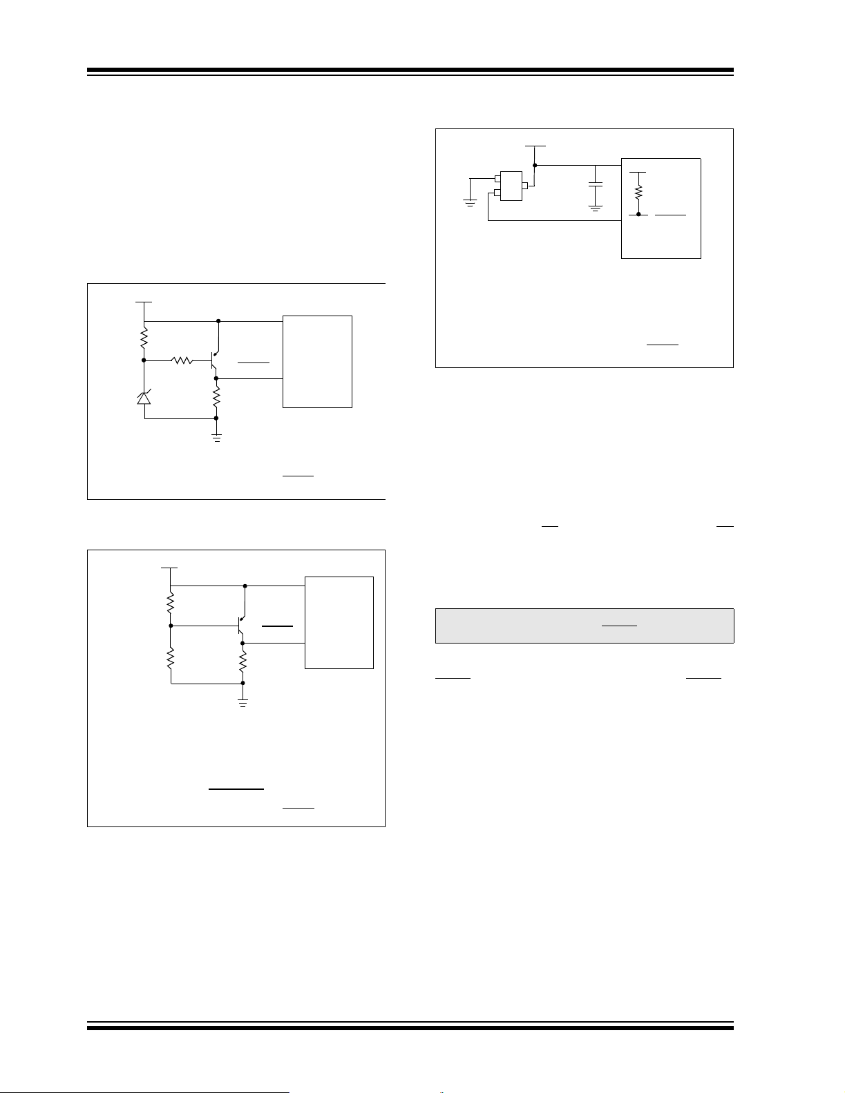
PIC10F220/222
8.8 Reset on Brown-out
A Brown-out is a condition where device power (VDD)
dips below its minimum value, but no t to zero, and the n
recovers. The device should be reset in the event of a
Brown-out.
To reset PIC10F220/222 devices when a Brown-out
occurs, external Brown-out protection circuits may be
built, as shown in Figure 8-7 and Figure 8-8.
FIGURE 8-7: BROWN-OUT
PROTECTION CIRCUIT 1
VDD
VDD
33k
VDD
MCLR
(2)
(1)
= 0.7V
PIC10F22X
.
PIC10F22X
(2)
.
Q1
40k
MCLR
(1)
10k
Note 1: This circuit will activate Reset when VDD goes
below Vz + 0.7V (where Vz = Zener voltage).
2: Pin must be configured as MCLR
FIGURE 8-8: BROWN-OUT
PROTECTION CIRCUIT 2
VDD
R1
Q1
R2
Note 1: This brown-out circuit is less expensive,
although less accurate. Transistor Q1 turns
off when V
that:
2: Pin must be configured as MCLR
DD is below a certain level such
V
DD •
40k
R1
R1 + R2
FIGURE 8-9: BROWN-OUT
PROTECTION CIRCUIT 3
VDD
MCP809
VSS
RST
Note 1: This Brown-out Protection circuit employs
2: Pin must be configured as MCLR
Bypass
Capacitor
VDD
Microchip Technology’s MCP809 microcontroller supervisor. There are 7 different
trip point selections to accommodate 5V to
3V systems.
VDD
MCLR
PIC10F22X
(2)
.
8.9 Power-Down Mode (Sleep)
A device may be powered down (Sleep) and later
powered up (wake-up from Sleep).
8.9.1 SLEEP
The Power-Down mode is entered by executing a
SLEEP instruction.
If enabled, the Watchdog Timer will be cleared but
keeps running, the TO
bit (STATUS<3>) is cleared and the oscillator driver is
turned off. The I/O ports maintain the status they had
before the SLEEP instruction was executed (driving
high, driving low or high-impedance).
Note: A Reset generated by a WDT time-out
does not drive the MCLR
For lowest cur rent consum ption while pow ered down,
the T0CKI input shoul d be at V
/VPP pin must be at a logic high level if MCLR is
MCLR
enabled.
bit (STATUS<4>) is set, the PD
pin low.
DD or VSS and the GP3/
DS41270A-page 42 Preliminary © 2005 Microchip Technology Inc.
Page 43

PIC10F220/222
8.9.2 WAKE-UP FROM SLEEP
The device can wake -up from Sleep through one of th e
following events:
1. An external Reset input on GP3/MC LR
when configured as MCLR
.
/VPP pin,
2. A Watchdog Timer time-out Reset (if WDT was
enabled).
3. A change on input pin GP0, GP1 or GP3 when
wake-up on change is enabled.
These events cause a device Reset. The TO
, PD
GPWUF bits can be used to determine the cause of
device Reset. The TO
occurred (a nd caused w ake-up). The PD
bit is cleared if a WDT time-out
bit, which is
set on power-up, is cleared when SLEEP is invoked.
The GPWUF bit indicates a change in state while in
Sleep at pins GP0 , GP1 or GP3 (sin ce the last file or bit
operation on GP port).
Caution: Right before entering Sleep, read the
input pins. When in Sleep, wake up
occurs when the values at the pins
change from the sta te they were in at th e
last reading. If a wake-up on change
occurs and t he pin s are no t read be fore
re-entering Sleep, a wake-up will occur
immediately even if no pins change
while in Sleep mode.
Note: The WDT is cleared when the device
wakes from Sleep, regardless of the
wake-up source.
8.10 Program Verification/Code
Protection
If the code protecti on bit has not be en programmed, the
on-chip program memory can be read out for
verification purposes.
The first 64 locations and the last location (Reset
vector) can be read, regardless of the code protection
bit setting.
8.12 In-Circuit Serial Programming
The PIC10F220/222 microcontrollers can be serially
programmed while in t he end a pplicati on circu it. Th is i s
simply done with two lines for clock and dat a, and three
other lines for power, ground and the programming
voltage. This allows customers to manufacture boards
with unprogrammed devices and then program the
microcontroller just before shipping the product. This
also allows the most recent firmware, or a custom
firmware, to be programmed.
The devices are placed into a Program/Verify mode by
holding the GP1 and GP0 pins low while raising the
(VPP) pin from VIL to VIHH (see programming
MCLR
specification). GP1 becomes the programming clock
and GP0 beco mes the progr amming data. Both GP1
and GP0 are Schmitt Trigger inputs in this mode.
After Reset, a 6-bit command is then supplied to the
device. Depending on the command , 16 b its of program
data are then supplied to or from the device, depending
if the command was a load or a read. For complete
details of serial programming, please refer to the
PIC10F220/222 Programming Specifications.
A typical In-Circuit Serial Programming connection is
shown in Figure 8-10.
FIGURE 8-10: TYPICAL IN-CIRCUIT
SERIAL PROGRAMMING
CONNECTION
To Nor mal
External
Connector
Signals
+5V
0V
V
PP
CLK
Data I/O
Connections
PIC10F22X
DD
V
VSS
MCLR/VPP
GP1
GP0
V
8.11 ID Locations
Four memory locations are designated as ID locations
where the user can store checksum or other code
To Nor mal
Connections
DD
identification numbers. These locations are not
accessible during normal execution, but are readable
and writable during program/verify.
Use only the lower 4 bits o f the ID locati ons and al ways
program the upper 8 bits as ‘0’s.
© 2005 Microchip Technology Inc. Preliminary DS41270A-page 43
Page 44

PIC10F220/222
NOTES:
DS41270A-page 44 Preliminary © 2005 Microchip Technology Inc.
Page 45
PIC10F220/222
9.0 INSTRUCTION SET SUMMARY
The PIC16 instruction set is highly orthogonal and is
comprised of three basic categories.
• Byte-oriented operations
• Bit-oriented operations
• Literal and control operations
Each PIC16 instruction is a 12-bit word divided into an
opcode, which specifies the instruction type, and one
or more operands which further specify the operation
of the instruction. The formats for each of the categories is presented in Figure 9-1, while the various
opcode fields are summarized in Table 9-1.
For byte-oriented instructions, ‘f’ represent s a file reg-
ister designator and ‘d’ represents a destination designator. The file regi ster designator s pecifies which fi le
register is to be used by the instruction.
The destination des ignator specifies w here the result of
the operation is to be placed. If ‘d’ is ‘0’, the result is
placed in the W register. If ‘d’ is ‘1’, the result is placed
in the file register specified in the instruction.
For bit-oriented instru ctions, ‘b’ represents a bit field
designator which selects the number of the bit affected
by the operation, while ‘f’ represents the number of the
file in which the bit is located.
For literal and control operations, ‘k’ represents an
8 or 9-bit constant or literal value.
All instructions are executed within a single instruction
cycle, unless a conditional test is true or the program
counter is changed as a result of an instruction. In this
case, the execution takes two instruction cycles. One
instruction cycle consists of four oscillator periods.
Thus, for an oscillator frequency of 4 MHz, the normal
instruction exec ution time is 1 μs. If a conditional test is
true or the program counter is changed as a result of an
instruction, the instruction execution time is 2 μs.
Figure 9-1 shows the three general formats that the
instructions can have. All examples in the figure use
the following format to represent a hexadecimal
number:
0xhhh
where ‘h’ signifies a hexadecimal digit.
FIGURE 9-1: GENERAL FORMAT FOR
INSTRUCTIONS
Byte-oriented file regi s ter operations
11 6 5 4 0
OPCODE d f (FILE #)
d = 0 for destination W
d = 1 for destination f
f = 5-bit file register address
Bit-oriented file register operations
11 8 7 5 4 0
OPCODE b (BIT #) f (FILE #)
TABLE 9-1: OPCODE FIELD
DESCRIPTIONS
Field Description
f Register File Address (0x00 to 0x7F)
W Working Register (accumulator)
b Bit Address within an 8-bit file register
k Literal field, constant data or label
x Don’t care location (= 0 or 1)
The assembler will generate code with x = 0. It is the
recommended form of use for compatibility with all
Microchip software tools.
d Destination select;
d = 0 (store result in W)
d = 1 (store result in file register ‘f’)
Default is d = 1
label Label name
TOS Top-of-Stack
PC Program Counter
WDT Watchdog Timer counter
TO Time-out bit
PD Power-down bit
dest Destination, either the W register or the specified regis-
[ ] Options
( ) Contents
italics User defined term (font is courier)
ter file location
→ Assigned to
< > Register bit field
∈ In the set of
b = 3-bit address
f = 5-bit file register address
Literal and control operations (except GOTO)
11 8 7 0
OPCODE k (literal)
k = 8-bit immediate value
Literal and control operations – GOTO instruction
11 9 8 0
OPCODE k (literal)
k = 9-bit immediate value
© 2005 Microchip Technology Inc. Preliminary DS41270A-page 45
Page 46

PIC10F220/222
TABLE 9-2: INSTRUCTION SET SUMMARY
Mnemonic,
Operands
ADDWF
ANDWF
CLRF
CLRW
COMF
DECF
DECFSZ
INCF
INCFSZ
IORWF
MOVF
MOVWF
NOP
RLF
RRF
SUBWF
SWAPF
XORWF
BCF
BSF
BTFSC
BTFSS
ANDLW
CALL
CLRWDT
GOTO
IORLW
MOVLW
OPTION
RETLW
SLEEP
TRIS
XORLW
Note 1: The 9th bit of the program counter will be forced to a ‘0’ by any instruction that writes to the PC except for
f,d
f,d
f
–
f, d
f, d
f, d
f, d
f, d
f, d
f, d
f
–
f, d
f, d
f, d
f, d
f, d
f, b
f, b
f, b
f, b
k
k
k
k
k
k
–
k
–
f
k
GOTO. See Section 4.7 “Program Counter”.
2: When an I/O register is modified as a function of itself (e.g. MOVF PORTB, 1), the value used will be that
value present on the pins thems elve s. For example , if the dat a latch is ‘1’ for a pi n configured as input and
is driven low by an external device, the data will be written back with a ‘0’.
3: The instruction TRIS f, where f = 6 causes the contents of the W register to be written to the tristate
latches of PORTB. A ‘1’ forces the pin to a high-impedance state and disables the output buffers.
4: If this instruction is executed on the TMR0 register (and, where applicable, d = 1), the prescaler will be
cleared (if assigned to TMR0).
Add W and f
AND W with f
Clear f
Clear W
Complement f
Decrement f
Decrement f, Skip if 0
Increment f
Increment f, Skip if 0
Inclusive OR W with f
Move f
Move W to f
No Operation
Rotate left f through Carry
Rotate right f through Carry
Subtract W from f
Swap f
Exclusive OR W with f
Bit Clear f
Bit Set f
Bit Test f, Skip if Clear
Bit Test f, Skip if Set
AND Literal with W
Call Subroutine
Clear Watchdo g Timer
Unconditional Branch
Inclusive OR Literal with W
Move Literal to W
Load OPTION Register
Return, Place Literal in W
Go into Standby Mode
Load TRIS Register
Exclusive OR Literal to W
Description Cycles
1
1
1
1
1
1
1
1
1
1
1
1
1
1
1
1
1
1
BIT-ORIENTED FILE REGISTER OPERATIONS
1
1
1
1
LITERAL AND CONTROL OPERATIONS
1
2
1
2
1
1
1
2
1
1
1
12-Bit Opcode
MSb LSb
0001
0001
0000
0000
0010
0000
0010
0010
0011
0001
0010
0000
0000
0011
0011
0000
0011
0001
0100
0101
0110
0111
1110
1001
0000
101k
1101
1100
0000
1000
0000
0000
1111
11df
01df
011f
0100
01df
11df
11df
10df
11df
00df
00df
001f
0000
01df
00df
10df
10df
10df
bbbf
bbbf
bbbf
bbbf
kkkk
kkkk
0000
kkkk
kkkk
kkkk
0000
kkkk
0000
0000
kkkk
ffff
ffff
ffff
0000
ffff
ffff
ffff
ffff
ffff
ffff
ffff
ffff
0000
ffff
ffff
ffff
ffff
ffff
ffff
ffff
ffff
ffff
kkkk
kkkk
0100
kkkk
kkkk
kkkk
0010
kkkk
0011
0fff
kkkk
Status
Affected
C,DC,Z
Z
Z
Z
Z
Z
None
Z
None
Z
Z
None
None
C
C
C,DC,Z
None
Z
None
None
None
None
Z
None
, PD
TO
None
Z
None
None
None
, PD
TO
None
Z
Notes
1,2,4
2,4
4
2,4
2,4
2,4
2,4
2,4
2,4
1,4
2,4
2,4
1,2,4
2,4
2,4
2,4
2,4
2
2
1
3
DS41270A-page 46 Preliminary © 2005 Microchip Technology Inc.
Page 47

9.1 Instruction Description
PIC10F220/222
ADDWF Add W and f
Syntax: [ label ] ADDWF f,d
Operands: 0 ≤ f ≤ 31
d ∈ [0,1]
Operation: (W) + (f) → (destination)
Status Affected: C, DC, Z
Description: Add the contents of the W register
and register ‘f’. If ‘d’ is’0’, the result
is stored in the W register. If ‘d’ is
‘1’, the result is stored back in
register ‘f’.
ANDLW And literal with W
Syntax: [ label ] ANDLW k
Operands: 0 ≤ k ≤ 255
Operation: (W).AND. (k) → (W)
Status Affected: Z
Description: The contents of the W register are
AND’ed with the eight-bit literal ‘k’.
The result is placed in the W
register.
BCF Bit Clear f
Syntax: [ label ] BCF f,b
Operands: 0 ≤ f ≤ 31
0 ≤ b ≤ 7
Operation: 0 → (f<b>)
Status Affected: None
Description: Bit ‘b’ in register ‘f’ is cleared.
BSF Bit Set f
Syntax: [ label ] BSF f,b
Operands: 0 ≤ f ≤ 31
0 ≤ b ≤ 7
Operation: 1 → (f<b>)
Status Affected: None
Description: Bit ‘b’ in register ‘f’ is set.
ANDWF AND W with f
Syntax: [ label ] ANDWF f,d
Operands: 0 ≤ f ≤ 31
d ∈ [0,1]
Operation: (W) .AND. (f) → (destination)
Status Affected: Z
Description: The contents of the W register are
AND’ed with register ‘f’. If ‘d’ is ‘0’,
the result is stored in the W register .
If ‘d’ is ‘1’, the result is stored back
in register ‘f’.
© 2005 Microchip Technology Inc. Preliminary DS41270A-page 47
BTFSC Bit Test f, Skip if Clear
Syntax: [ label ] BTFSC f,b
Operands: 0 ≤ f ≤ 31
0 ≤ b ≤ 7
Operation: skip if (f<b>) = 0
Status Affected: None
Description: If bit ‘b’ in register ‘ f’ is ‘0’, then the
next instruction is skipped.
If bit ‘b’ is ‘0’, then the next instruc-
tion fetched during the current
instruction execution is discarded,
and a NOP is executed instead,
making this a 2-cycle instruction.
Page 48

PIC10F220/222
BTFSS Bit Test f, Skip if Set
Syntax: [ label ] BTFSS f,b
Operands: 0 ≤ f ≤ 31
0 ≤ b < 7
Operation: skip if (f<b>) = 1
Status Affected: None
Description: If bit ‘b’ in regis ter ‘f’ i s ‘1’, the n the
next instruction is skipped.
If bit ‘b’ is ‘1’, the n the nex t ins tru c-
tion fetched during the current
instruction execution, is discarded
and a NOP is executed instead,
making this a 2-cycle instruction.
CALL Subroutine Call
Syntax: [ label ] CALL k
Operands: 0 ≤ k ≤ 255
Operation: (PC) + 1→ Top-of-Stack;
k → PC<7:0>;
(Status<6:5>) → PC<10:9>;
0 → PC<8>
Status Affected: None
Description: Subroutine call. First, return
address (PC + 1) is pushed onto
the stack. The eight-bit immediate
address is loaded into PC bits
<7:0>. The upper bits PC<10:9>
are loaded from Status<6:5>,
PC<8> is cleared. CALL is a
two-cycle instruction.
CLRW Clear W
Syntax: [ label ] CLRW
Operands: None
Operation: 00h → (W);
1 → Z
Status Affected: Z
Description: The W register is cleared. Zero bit
(Z) is set.
CLRWDT Clear Watchdog Timer
Syntax: [ label ] CLRWDT
Operands: None
Operation: 00h → WDT;
0 → WDT prescaler (if assigned);
1 → TO;
1 → PD
Status Affected: TO, PD
Description: The CLRWDT instruction resets the
WDT . It a lso reset s the prescaler , if
the prescaler is assigned to the
WDT and not Timer0. Status bits
TO and PD are set.
CLRF Clear f
Syntax: [ label ] CLRF f
Operands: 0 ≤ f ≤ 31
Operation: 00h → (f);
1 → Z
Status Affected: Z
Description: The contents of register ‘f’ are
cleared and the Z bit is set.
DS41270A-page 48 Preliminary © 2005 Microchip Technology Inc.
COMF Complement f
Syntax: [ label ] COMF f,d
Operands: 0 ≤ f ≤ 31
d ∈ [0,1]
Operation: (f
Status Affected: Z
Descriptio n: The contents of r egister ‘f’ are
) → (dest)
complemented. If ‘d’ is ‘0’, the
result is stored in the W register. If
‘d’ is ‘1’, the result is stor ed back in
register ‘f’.
Page 49

PIC10F220/222
DECF Decrement f
Syntax: [ label ] DECF f,d
Operands: 0 ≤ f ≤ 31
d ∈ [0,1]
Operation: (f) – 1 → (dest)
Status Affected: Z
Description: Decrement register ‘f’. If ‘d’ is ‘0’,
the result is stored in the W
register. If ‘d’ is ‘1’, the result is
stored back in register ‘f’.
DECFSZ Decrement f, Skip if 0
Syntax: [ label ] DECFSZ f,d
Operands: 0 ≤ f ≤ 31
d ∈ [0,1]
Operation: (f) – 1 → d; skip if result = 0
Status Affected: None
Description: The contents of regis ter ‘f’ are dec-
remented. If ‘d’ is ‘0’, the result is
placed in the W regis ter. If ‘d’ is ‘1’,
the result is placed back in register
‘f’.
If the result is ‘0’, the next instruc-
tion, which is already fetched, is
discarded and a NOP is executed
instead making it a two-cycle
instruction.
INCF Increment f
Syntax: [ label ] INCF f,d
Operands: 0 ≤ f ≤ 31
d ∈ [0,1]
Operation: (f) + 1 → (dest)
Status Affected: Z
Descriptio n: The contents of r egister ‘f’ are
incremented. If ‘d’ is ‘0’, the result
is placed in the W register. If ‘d’ is
‘1’, the result is placed back in
register ‘f’.
INCFSZ Increment f, Skip if 0
Syntax: [ label ] INCFSZ f,d
Operands: 0 ≤ f ≤ 31
d ∈ [0,1]
Operation: (f) + 1 → (dest), skip if result = 0
Status Affected: None
Descriptio n: The contents of r egister ‘f’ are
incremented. If ‘d’ is ‘0’, the result
is placed in the W register. If ‘d’ is
‘1’, the result is placed back in
register ‘f’.
If the result is ‘0’, then the next
instruction, which is already
fetched, is discarded and a NOP is
executed instead making it a
two-cycle instruction.
GOTO Unconditional Branch
Syntax: [ label ] GOTO k
Operands: 0 ≤ k ≤ 51 1
Operation: k → PC<8:0>;
Status<6:5> → PC<10:9>
Status Affected: None
Description: GOTO is an unconditional branch.
The 9-bit immediate value is
loaded into PC bits <8:0>. The
upper bits of PC are loaded from
Status<6:5>. GOTO is a two-cycle
instruction.
© 2005 Microchip Technology Inc. Preliminary DS41270A-page 49
IORLW Inclusive OR literal with W
Syntax: [ label ] IORLW k
Operands: 0 ≤ k ≤ 255
Operation: (W) .OR. (k) → (W)
Status Affected: Z
Description: The contents of the W register are
OR’ed with the eight bit literal ‘k’.
The result is placed in the W
register.
Page 50

PIC10F220/222
IORWF Inclusive OR W with f
Syntax: [ label ] IORWF f,d
Operands: 0 ≤ f ≤ 31
d ∈ [0,1]
Operation: (W).OR. (f) → (dest)
Status Affected: Z
Description: Inclusive OR the W register with
register ‘f’. If ‘d’ is ‘0’, the result is
placed in the W regis ter. If ‘d’ is ‘1’,
the result is placed back in register
‘f’.
MOVF Move f
Syntax: [ label ] MOVF f,d
Operands: 0 ≤ f ≤ 31
d ∈ [0,1]
Operation: (f) → (dest)
Status Affected: Z
Description: The contents of register ‘f’ are
moved to destina tion ‘d’. If ‘d’ is ‘0’,
destination is the W register. If ‘d’
is ‘1’, the destination is file registe r
‘f’. ‘d’ = 1 is useful as a test of a file
register, since status flag Z is
affected.
MOVWF Move W to f
Syntax: [ label ] MOVWF f
Operands: 0 ≤ f ≤ 31
Operation: (W) → (f)
Status Affected: None
Description: Move data from the W register to
register ‘f’.
NOP No Operation
Syntax: [ label ] NOP
Operands: None
Operation: No operation
Status Affected: None
Description: No operation.
MOVLW Move Literal to W
Syntax: [ label ] MOVLW k
Operands: 0 ≤ k ≤ 255
Operation: k → (W)
Status Affected: None
Description: The eight-bit literal ‘k’ is loaded
into the W register . The don’ t cares
will assembled as ‘0’s.
OPTION Load OPTION Register
Syntax: [ label ] OPTION
Operands: None
Operation: (W) → OPTION
Status Affected: None
Description: The content of the W register is
loaded into the OPTION register.
DS41270A-page 50 Preliminary © 2005 Microchip Technology Inc.
Page 51

PIC10F220/222
RETLW Return with Literal in W
Syntax: [ label ] RETLW k
Operands: 0 ≤ k ≤ 255
Operation: k → (W);
TOS → PC
Status Affected: None
Description: The W register is loaded with the
eight-bit literal ‘k’. The program
counter is loaded from the top of
the stack (the return address). This
is a two-cycle instructi on.
RLF Rotate Left f through Carry
Syntax: [ label ] RLF f,d
Operands: 0 ≤ f ≤ 31
d ∈ [0,1]
Operation: See description below
Status Affected: C
Description: The contents of register ‘f’ are
rotated one bit to the left through
the Carry Flag. If ‘d’ is ‘0’, the
result is placed in the W reg ister. If
‘d’ is ‘1’, the res ult is stored b ack in
register ‘f’.
C
register ‘f’
SLEEP Enter SLEEP Mode
Syntax:
Operands: None
Operation: 00h → WDT;
Status Affected: TO, PD, RBWUF
Description: Time-out S tat us bit (TO
SUBWF Subtract W from f
Syntax:
Operands: 0 ≤ f ≤ 31
Operation: (f) – (W) → (dest)
Stat us Affected: C, DC, Z
Description: Subtract (2’s complem ent met hod)
[label ]
0 → WDT prescaler;
1 → TO
0 → PD
Power-Down Status bit (PD
cleared.
RBWUF is unaffected.
The WDT and its prescaler are
cleared.
The processor is put in to Sleep
mode with the oscillato r st op ped .
See section on Sleep for more
details.
[label ] SUBWF f,d
d ∈ [0,1]
the W register from register ‘ f’. If ‘d’
is ‘0’, the result is stored in the W
register. If ‘d’ is ‘1’, the result is
stored back in register ‘f’.
SLEEP
;
) is set. The
) is
RRF Rotate Right f through Carry
Syntax: [ label ] RRF f,d
Operands: 0 ≤ f ≤ 31
d ∈ [0,1]
Operation: See description below
Status Affected: C
Description: The contents of register ‘f’ are
rotated one bit to the right through
the Carry Flag. If ‘d’ is ‘0’, the
result is placed in the W reg ister. If
‘d’ is ‘1’, the result is placed back
in register ‘f’.
C
© 2005 Microchip Technology Inc. Preliminary DS41270A-page 51
register ‘f’
SWAPF Swap Nibbles in f
Syntax: [ label ] SWAPF f,d
Operands: 0 ≤ f ≤ 31
d ∈ [0,1]
Operation: (f<3:0>) → (dest<7:4>);
(f<7:4>) → (dest<3:0>)
Status Affected: None
Description: The upper and lower nibbles of
register ‘f’ are exchanged. If ‘d’ is
‘0’, the result is placed in W
register. If ‘d’ is ‘1’, the result is
placed in register ‘f’.
Page 52

PIC10F220/222
TRIS Load TRIS Register
Syntax: [ label ] TRIS f
Operands: f =
Operation: (W) → TRIS register f
Status Affected: None
Description: TRIS register ‘f’ (f = 6 or 7) is
XORLW Exclusive OR literal with W
Syntax:
Operands: 0 ≤ k ≤ 255
Operation: (W) .XOR. k → (W)
Status Affected: Z
Description: The contents of the W register are
6
loaded with the contents of the W
register
[label ]XORLW k
XOR’ed with the eight- bit lite ral ‘k ’.
The result is placed in the W
register.
XORWF Exclusive OR W with f
Syntax: [ label ] XORWF f,d
Operands: 0 ≤ f ≤ 31
d ∈ [0,1]
Operation: (W) .XOR. (f) → (dest)
Status Affected: Z
Description: Exclusive OR the contents of the
W register with register ‘f’. If ‘d’ is
‘0’, the result is stored in the W
register. If ‘d’ is ‘1’, the resu lt is
stored back in register ‘f’.
DS41270A-page 52 Preliminary © 2005 Microchip Technology Inc.
Page 53

10.0 ELECTRICAL CHARACTERISTICS
PIC10F220/222
Absolute Maximum Ratings
(†)
Ambient temperature under bias.............................................................................................................-40°C to +125°C
Storage temperature ...............................................................................................................................-65°C to +150°C
Voltage on V
Voltage on MCLR
Voltage on all other pins with respect to V
Total power dissipation
Max. current out of V
Max. current into V
Input clamp current, I
Output clamp current, I
DD with respect to VSS ..................................................................................................................0 to +6.5V
with respect to VSS............................................................. ...... ...... ..... ...............................0 to +13.5V
SS ..................................................................................-0.3V to (VDD + 0.3V)
(1)
.....................................................................................................................................200 mW
SS pin................................ ...... ...... ..... ...... ...... ........................................................ ..... ...........80 mA
DD pin........................................................................................................................................80 mA
IK (VI < 0 or VI > VDD)......................................................................................................................±20 mA
OK (VO < 0 or VO > VDD)..............................................................................................................±20 mA
Max. output current sunk by any I/O pin .................................................................................................................25 mA
Max. output current sourced by any I/O pin............................................................................................................25 mA
Max. output current sourced by I/O port .................................................................................................................75 mA
Max. output current sunk by I/O port ......................................................................................................................75 mA
Note 1: Power dissipation is calculated as fol lows: P
†
NOTICE: Stresses above those listed under “Absolute Maximum Ratings” may cause permanent damage to the
DIS = VDD x {IDD – ∑ IOH} + ∑ {(VDD – VOH) x IOH} + ∑(VOL x IOL)
device. This is a stress rating only and functional operation of the device at those or any other conditions above
those indi c at e d in t he o pe rat i o n l is tin g s o f t his s pec if i ca t io n is not i mp li e d. Ex po su r e to m ax im um r at i ng c ond it i on s
for extended periods may affect device reliability.
© 2005 Microchip Technology Inc. Preliminary DS41270A-page 53
Page 54

PIC10F220/222
FIGURE 10-1: VOLTAGE-FREQUENCY GRAPH, -40°C ≤ TA ≤ +125°C
6.0
5.5
5.0
4.5
DD
V
(Volts)
4.0
3.5
3.0
2.5
2.0
0
410
8
Frequency (MHz)
20
25
DS41270A-page 54 Preliminary © 2005 Microchip Technology Inc.
Page 55

10.1 DC Characteristics: PIC10F220/222 (Industrial)
PIC10F220/222
DC Characteristics
Param
No.
D001 V
Sym Characteristic Min Typ
DD Supply Voltage 2.0 — 5.5 V See Figure 10-1
D002 VDR RAM Data Retention Voltage
D003 VPOR VDD Start Voltage to ensure
Power-on Reset
D004 S
VDD VDD Rise Rate to ensure
Power-on Reset
D010 I
DD Supply Current
D020 IPD Power-down Current
D022 ΔIWDT WDT Current
D024 ΔI
ADC A/D Current —80TBDμAVDD = 2.0V
(3)
(4)
(4)
Standard Operating Conditions (unless otherwise specified)
Operating Temperature -40°C ≤ T
(1)
Max Units Conditions
(2)
— 1.5* — V Device in Sleep mode
A ≤ +85°C (industrial)
—Vss— VSee Section 8.4 “Power-on
Reset (POR)” for details
0.05* — — V/ms See Section 8.4 “Power-on
Reset (POR)” for details
—
170
—
—
—
350
250
450
TBD
TBD
TBD
TBD
μA
FOSC = 4 MHz, VDD = 2.0V
μA
μA
μA
OSC = 4 MHz, VDD = 5.0V
F
OSC = 8 MHz, VDD = 2.0V
F
F
OSC = 8 MHz, VDD = 5.0V
—0.1TBDμAVDD = 2.0V
—1.0TBDμAVDD = 2.0V
Legend: TBD = To Be Determined.
* These parameters are characterized but not tested.
Note 1: Data in the Typical (“Typ”) column is based on characterization results at 25°C. This data is for design
guidance only and is not tested.
2: This is the limit to which V
DD can be lowered in Sleep mode without losing RAM data.
3: The supply current is mainly a function of the operating voltage and frequency. Other factors such as bus
loading, bus rate, internal code execution pattern and temperature also have an impact on the current
consumption.
a) The test conditions for all I
All I/O pins tristated, pu ll ed to V
DD measurements in active operation mode are:
SS, T0CKI = VDD, MCLR = VDD; WDT enabled/disab led as s pec ifi ed .
b) For standby current measurements, the conditions are the same, except that the device is in Sleep
mode.
4: Power-down current is measured with the part in Sleep mode, with all I/O pins in high-impedance state
and tied to V
DD or VSS.
© 2005 Microchip Technology Inc. Preliminary DS41270A-page 55
Page 56

PIC10F220/222
10.2 DC Characteristics: PIC10F220/222 (Extended)
DC Characteristics
Param
No.
D001 V
Sym Characteristic Min Typ
DD Supply Voltage 2.0 5.5 V See Figure 10-1
D002 VDR RAM Data Retention Voltage
D003 VPOR VDD Start Voltage to ensure
Power-on Reset
D004 S
VDD VDD Rise Rate to ensure
Power-on Reset
D010 I
DD Supply Current
D020 IPD Power-down Current
D022 ΔIWDT WDT Current
D024 ΔI
ADC A/D Current —80TBDμAVDD = 2.0V
(3)
(4)
(4)
Standard Operating Conditions (unless otherwise specified)
Operating Temperature -40°C ≤ T
(1)
Max Units Conditions
(2)
— 1.5* — V Device in Sleep mode
A ≤ +125°C (extended)
—Vss— VSee Section 8.4 “Power-on
Reset (POR)” for details
0.05* — — V/ms See Section 8.4 “Power-on
Reset (POR)” for details
—
170
—
—
—
350
250
450
TBD
TBD
TBD
TBD
μA
FOSC = 4 MHz, VDD = 2.0V
μA
μA
μA
OSC = 4 MHz, VDD = 5.0V
F
OSC = 8 MHz, VDD = 2.0V
F
F
OSC = 8 MHz, VDD = 5.0V
—0.1TBDμAVDD = 2.0V
—1.0TBDμAVDD = 2.0V
Legend: TBD = To Be Determined.
* These parameters are characterized but not tested.
Note 1: Data in the Typical (“Typ”) column is based on characterization results at 25°C. This data is for design
guidance only and is not tested.
2: This is the limit to which V
DD can be lowered in Sleep mode without losing RAM data.
3: The supply current is mainly a function of the operating voltage and frequency. Other factors such as bus
loading, bus rate, internal code execution pattern and temperature also have an impact on the current
consumption.
a) The test conditions for all I
All I/O pins tristated, pulle d to V
DD measurements in active operation mode are:
SS, T0CKI = VDD, MCLR = VDD; WDT enabled/disabled as specified.
b) For standby current measurements, the conditions are the same, except that the device is in Sleep
mode.
4: Power-down current is measured with the part in Sleep mode, with all I/O pins in high-impedance state
and tied to V
DD or VSS.
DS41270A-page 56 Preliminary © 2005 Microchip Technology Inc.
Page 57

PIC10F220/222
TABLE 10-1: DC CHARACTERISTICS: PIC10F220/222 (Industrial, Extended)
Standard Operating Conditions (unless otherwise specified)
DC CHARACTERISTICS
Param
Sym Characteristic Min Typ† Max Units Conditions
No.
V
IL Input Low Voltage
Operating temperature-40°C ≤ T
-40°C ≤ T
Operating voltage V
DD range as described in DC specification
I/O ports:
D030 with TTL buffer Vss — 0.8V V For all 4.5 ≤ V
D030A Vss — 0.15 V
D031 with Schmitt Trigger buffer Vss — 0.15 V
D032 MCLR
V
IH Input High Voltage
, T0CKI Vss — 0.15 VDD V
I/O ports: —
D040 with TTL buffer 2.0 — V
D040A 0.25 V
D041 with Schmitt Trigger buffer 0.85 V
D042 MCLR
D070 I
PUR GPIO weak pull-up current
IIL Input Leakage Current
, T0CKI 0.85 VDD —VDD V
(3)
(1,2)
DD + 0.8 — VDD V Otherwise
DD —VDD V For entire VDD range
TBD 250 TBD μAVDD = 5V, VPIN = VSS
D060 I/O ports — — ±1 μAVss ≤ VPIN ≤ VDD, Pin at
D061 GP3/MCLR
D061A GP3/MCLR
(4)
(5)
——±30μAVss ≤ VPIN ≤ VDD
——±5μAVss ≤ VPIN ≤ VDD
Output Low Voltage
D080 I/O ports — — 0.6 V I
D080A — — 0.6 V I
Output High Voltage
D090 I/O ports
(2)
D090A V
VDD – 0.7 — — V IOH = -3.0 mA, VDD = 4.5V,
DD – 0.7 — — V IOH = -2.5 mA, VDD = 4.5V,
Capacitive Loading Specs
on Output Pins
D101 All I/O pins — — 50* pF
Legend: TBD = To Be Determined.
† Data in “Typ” column is at 5V, 25°C unless otherwise stated. These parameters are for design guidance only and are not
tested.
* These parameters are for design guidance only and are not tested.
Note 1: The leakage current on the MCLR
pin is strongly dependent on the applied voltage level. The specified levels represent
normal operating conditions. Higher leakage current may be measured at different input voltages.
2: Negative current is defined as coming out of the pin.
3: Does not include GP3. For GP3 see parameters D061 and D061A.
4: This specification applies to GP3/MCLR
configured as external MCLR and GP3/MCLR configured as input with internal
pull-up enabled.
5: This specification applies when GP3/MCLR
circuit is higher than the standard I/O logic.
MCLR
is configured as an input with pull-up disabled. The leakage current of the
A ≤ +85°C (industrial)
A ≤ +125°C (extended)
DD ≤ 5.5V
DD V Otherwise
DD V
DD V4.5 ≤ VDD ≤ 5.5V
high-impedance
OL = 8.5 mA, VDD = 4.5V,
-40°C to +85°C
OL = 7.0 mA, VDD = 4.5V,
+85°C to +125°C
-40°C to +85°C
+85°C to +125°C
© 2005 Microchip Technology Inc. Preliminary DS41270A-page 57
Page 58

PIC10F220/222
TABLE 10-2: PULL-UP RESISTOR RANGES
VDD (Volts) Temperature (°C) Min Typ Max Units
GP0/GP1
2.0 -40 TBD TBD TBD Ω
25 TBD TBD TBD Ω
85 TBD TBD TBD Ω
125 TBD TBD TBD Ω
5.5 -40 TBD TBD TBD Ω
25 TBD TBD TBD Ω
85 TBD TBD TBD Ω
125 TBD TBD TBD Ω
GP3
2.0 -40 TBD TBD TBD Ω
25 TBD TBD TBD Ω
85 TBD TBD TBD Ω
125 TBD TBD TBD Ω
5.5 -40 TBD TBD TBD Ω
25 TBD TBD TBD Ω
85 TBD TBD TBD Ω
125 TBD TBD TBD Ω
Legend: TBD = To Be Determined.
* These parameters are characterized but not tested.
DS41270A-page 58 Preliminary © 2005 Microchip Technology Inc.
Page 59

PIC10F220/222
10.3 Timing Parameter Symbology and Load Conditions
The timing parameter symbols have been created following one of the following formats:
1. TppS2ppS
2. TppS
T
F Frequency T Time
Lowercase subscripts (pp) and their meanings:
pp
2to mcMCLR
ck CLKOUT osc Oscillator
cy Cycle time os OSC1
drt Device Reset Timer t0 T0CKI
io I/O port w dt Watchdog Timer
Uppercase letters and their meani ngs:
S
FFall PPeriod
HHigh RRise
I Invalid (high-impedance) V Valid
L Low Z High-impedance
FIGURE 10-2: LOAD CONDITIONS
CL = 50 pF for all pins
pin
CL
VSS
TABLE 10-3: CALIBRATED INTERNAL RC FREQUENCIES
Standard Operating Conditions (unless otherwise specified)
AC Characteristics
Param
No.
F10 FOSC Internal Calibrated
Legend: TBD = To Be Determined.
Note 1: To ensure these oscillator frequency tolerances, V
Sym Characteristic
INTOSC Frequency
* These parameters are characterized but not tested.
† Data in the Typical (“T y p”) c ol umn is at 5V, 25°C u nless otherwise stated. These p arameters are for design
guidance only and are not tested.
the device as possible. 0.1 μF and 0.01 μF values in parallel are recommended.
2: The 4 MHz clock is derived from the 8 MHz oscillator. To obtain 4 MHz tolerance values, divide the
appropriate 8 MHz value by 2.
Operating Temperature -40°C ≤ T
(1), (2)
Freq
Tolerance
±1% 7.92 8 8.08 MHz VDD and Temperature TBD
±2% 7.84 8 8.16 MHz 2.5V ≤ V
±5% 7.60 8 8.4 MHz 2.0V ≤ V
Min Typ† Max Units Conditions
DD and VSS must be capacitivel y decoupled as close to
-40°C ≤ T
A ≤ +85°C (industrial)
A ≤ +125°C (extended)
DD ≤ 5.5V
Temperature 0 - 85°C
DD ≤ 5.5V
-40°C ≤ T
-40°C ≤ T
A ≤ +85°C (industrial)
A ≤ +125°C (extended )
© 2005 Microchip Technology Inc. Preliminary DS41270A-page 59
Page 60
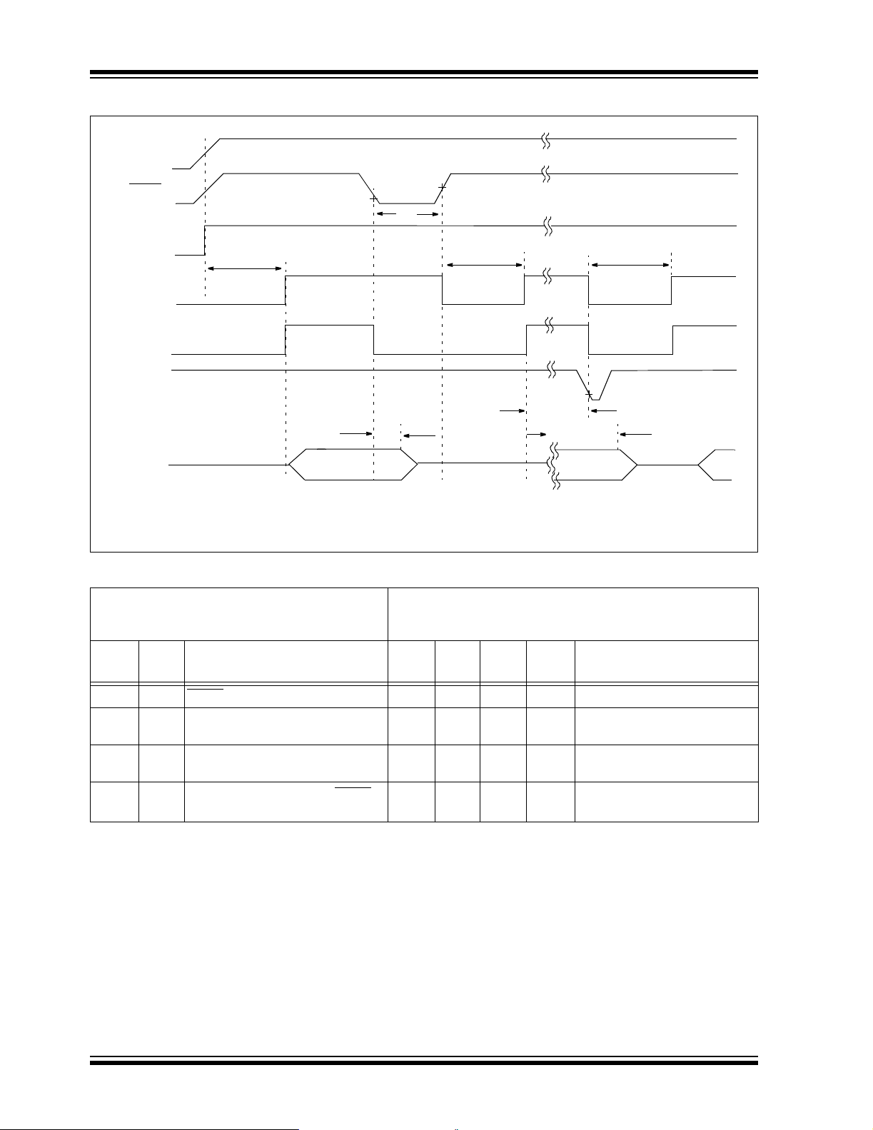
PIC10F220/222
FIGURE 10-3: RESET, WATCHDOG TIMER AND DEVICE RESET TIMER TIMING
VDD
MCLR
30
Internal
POR
DRT
Time-out
Internal
Reset
Watchdog
Timer
Reset
I/O pin
32
(2)
34
(1)
32
32
31
34
Note 1: I/O pins must be taken out of high-impedance mode by enabling the output drivers in software.
2: Runs on Power-on Reset only.
TABLE 10-4: RESET, WATCHDOG TIMER AND DEVICE RESET TIMER
Standard Op eratin g Conditi ons (un less otherw ise spec ifie d)
AC Characteristics
Param
No.
Sym Characteristic Min Typ
30 TMCLMCLR Pulse Width (low) 2000* — — ns VDD = 5.0V
31 T
WDT Watchdog Timer Time-out Period
(no prescaler)
32 T
34 T
DRT Device Reset Timer Period 0.5*
IOZ I/O High-Impedance from MCLR
Low
* These parameters are characterized but not tested.
Note 1: Data in the Typical (“Ty p”) col umn is at 5V, 25°C unl ess o therwi se st ated . These pa ram eters ar e for des ign
guidance only and are not tested.
Operating Temperature -40°C ≤ TA ≤ +85°C (industrial)
A ≤ +125°C (extended)
msmsVDD = 5.0V (Industrial)
DD = 5.0V (Extended)
V
VDD = 5.0V (Industrial)
V
DD = 5.0V (Extended)
(1)
9*
9*
18*
18*
1.125*
0.5*
1.125*2*2.5*msms
-40°C ≤ T
Max Units Conditions
30*
40*
— — 2000* ns
DS41270A-page 60 Preliminary © 2005 Microchip Technology Inc.
Page 61
FIGURE 10-4: TIMER0 CLOCK TIMINGS
T0CKI
40 41
TABLE 10-5: TIMER0 CLOCK REQUIREMENTS
Standard Operating Conditions (unless otherwise specified)
AC Characteristics
Param
No.
Sym Characteristic Min Typ
Operating Temperature -40°C ≤ TA ≤ +85°C (industrial)
42
-40°C ≤ T
PIC10F220/222
A ≤ +125°C (extended)
(1)
Max Units Conditions
40 Tt0H T0CKI High Pulse
Width
41 Tt0L T0CKI Low Pulse
Width
42 Tt0P T0CKI Period 20 or T
* These parameters are characterized but not tested.
Note 1: Data in the Typical (“Typ”) column is at 5V, 25°C unless oth erw is e st a ted . These parameters are for desig n
guidance only and are not tested.
No Prescaler 0 .5 T
With Prescaler 10* — — ns
No Prescaler 0 .5 T
With Prescaler 10* — — ns
CY + 20* — — ns
CY + 20* — — ns
CY + 40* N — — ns Whichever is greater.
N = Prescale Value
(1, 2, 4,..., 256)
© 2005 Microchip Technology Inc. Preliminary DS41270A-page 61
Page 62

PIC10F220/222
TABLE 10-6: A/D CONVERTER CHARACTERISTICS
Param
No.
A01 NR Resolution — — 8 bits bit
A02 E
A03 EIL Integral Error — — TBD LSb VDD = 5.0V
A04 EDL Differential Error — — TBD LSb No missing codes to 8 bits
A05 EFS Full-scale Ran ge 2.2* — 5.5* V VDD
A06 EOFF Offset Error — — TBD LSb VREF = 5.0V
A07 E
A10 — Monotonicity — guaranteed
A25 VAIN Analog Input Voltage — VDD —V
A30 Z
Note 1: Total Absolute Error includes integral, differential, offset and gain errors.
Sym Characteristic Min Typ† Max Units Conditions
ABS Total Absolute Error*
GN Gain Error — — TBD LSb VREF = 5.0V
AIN Recommended Impedance
of Analog Vol t age Source
* These parameters are characterized but not tested.
† Data in the “Typ” column is at 5.0V, 25°C unless otherwise stated. These parameters are for design
guidance only are not tested.
2: The A/D conversion result never decreases with an increase in the input voltage and has no missing
codes.
REF current is from external VREF or VDD pin, whichever is selected as reference input.
3: V
4: When A/D is off, it will not consume any current other than leakage current. The power-down current
specification includes any such leakage from the A/D module.
(1)
——TBDLSbVDD = 5.0V
V
DD = 5.0V
(2)
——VSS ≤ VAIN ≤ VREF+
——10kΩ
DS41270A-page 62 Preliminary © 2005 Microchip Technology Inc.
Page 63

PIC10F220/222
11.0 DEVELOPMENT SUPPORT
The PICmicro® microcontrollers are supported with a
full range of ha rdware a nd softwa re develo pment to ols:
• Integrated Development Environment
- MPLAB
• Assemblers/Compilers/Linkers
- MPASMTM Assembler
- MPLAB C18 and MPLAB C30 C Compilers
-MPLINK
MPLIB
- MPLAB ASM30 Assembler/Linker/Library
• Simulators
- MPLAB SIM Software Simulator
•Emulators
- MPLAB ICE 2000 In-Circuit Emulator
- MPLAB ICE 4000 In-Circuit Emulator
• In-Circuit Debugger
- MPLAB ICD 2
• Device Programmers
- PICSTART
- MPLAB PM3 Device Programmer
• Low-Cost Demonstration and Development
Boards and Evaluation Kits
®
IDE Software
TM
Object Linker/
TM
Object Librarian
®
Plus Development Programmer
11.1 MPLAB Integrated Development Environment Software
The MPLAB IDE so ftware brin gs an ease of sof tware
development previously unseen in the 8/16-bit microcontroller market. The MPLAB IDE is a Windows
operating system-based application that contains:
• A single graphical interface to all debugging tools
- Simulator
- Programmer (sold separately)
- Emulator (sold separately)
- In-Circuit Debugger (sol d separately)
• A full-featured editor with color-coded context
• A multiple project manager
• Customizable data windows with direct edit of
contents
• High-level source code debugging
• Visual device initializer for easy register
initialization
• Mouse over variable inspection
• Drag and drop variables from source to watch
windows
• Extensive on-line help
• Integration of select third party tools, such as
HI-TECH Software C Compilers and IAR
C Compilers
The MPLAB IDE allows you to:
• Edit your s ource files (either assembly or C)
• One touch assemble (or compile) and download
to PICmicro MCU emulator and simulator tools
(automatically updates all project information)
• Debug using:
- Source files (assembly or C)
- Mixed assembly and C
- Machine code
MPLAB IDE supports multiple debugging tools in a
single development paradigm, from the cost-effective
simulators, through low-cost in-circuit debuggers, to
full-featured emulators. This eliminates the learning
curve when upgrading to tools with increased flexibility
and power.
®
© 2005 Microchip Technology Inc. Preliminary DS41270A-page 63
Page 64

PIC10F220/222
11.2 MP ASM Assembler
The MPASM Assembler is a full-featured, universal
macro assembler for all PICmicro MCUs.
The MPASM Assembler generates relocatable object
files for the MPLINK Ob ject Linker, Intel
files, MAP files to detail memory usage and symbol
reference, absolute LST files that contain source lines
and generated machine code and COFF files for
debugging.
The MPASM Assembler features include:
• Integration into MPLAB IDE projects
• User-defined macros to streamline
assembly code
• Conditional assembly for multi-purpose
source files
• Directives that allow complete control over the
assembly process
®
standard HEX
11. 3 MPLAB C18 and MPLAB C30
C Compilers
The MPLAB C18 and MPLAB C30 Code Development
Systems are complete ANSI C compilers for
Microchip’s PIC18 family of microcontrollers and
dsPIC30F family of digital signal controllers. These
compilers provide powerful integration capabilities,
superior code optimization and ease of use not found
with other compilers.
For easy source level debuggi ng, the compil ers provide
symbol information that is opt imized to the MPLAB IDE
debugger.
11. 4 MPLINK Object Linker/
MPLIB Object Librarian
The MPLINK Object Linker combines relocatable
objects created by the MPASM Assembler and the
MPLAB C18 C Compiler. It can link relocatable objects
from precompiled libraries, using directives from a
linker script.
The MPLIB Object Librar ian manag es the cre ation an d
modification of library files of precompiled code. When
a routine from a library is called from a source file , only
the modules that contain that routine will be linked in
with the application. This allows large libraries to be
used efficiently in many different applications.
The object linker/library features include:
• Efficient linking of single libraries instead of many
smaller files
• Enhanced code maintainability by grouping
related modules together
• Flexible creation of libraries with easy module
listing, replacement, deletion and extraction
11.5 MPLAB ASM30 Assembler, Linker and Librarian
MPLAB ASM30 Assembler produces relocatable
machine code from symbolic assembly language for
dsPIC30F devices. MPLAB C30 C Compiler uses the
assembler to produce its object file. The assembler
generates relocatable object files that can then be
archived or linke d with other relocat able object fi les and
archives t o cr eat e an e xec utabl e fi le. Notab le f eat ures
of the assembler include:
• Support for the entire dsPIC30F instruction set
• Support for fixed-point and floating-point data
• Command line interface
• Rich directive set
• Flexible macro language
• MPLAB IDE compatibility
11. 6 MPLAB SIM Software Simulator
The MPLAB SIM Software Simulator allows code
developmen t in a PC-hosted env ironment by simu lating the PICmicro MCUs and dsPIC® DSCs on an
instruction level. On any given instruction, the data
areas can be examined or modified and stimuli can be
applied from a comprehensive stimulus controller.
Registers can be logged to files for further run-time
analysis. The trace buffer and logic analyzer display
extend the power of the simulator to record and track
program ex ecution, actions on I/O, as well as intern al
registers.
The MPLAB SIM Software Simulator fully supports
symbolic debugging using the MPLAB C18 and
MPLAB C30 C Compilers, and the MPASM and
MPLAB ASM30 Assemblers. The software simulator
offers the flexibility to develop and debug code outside
of the laboratory environment, making it an excellent,
economical software development tool.
DS41270A-page 64 Preliminary © 2005 Microchip Technology Inc.
Page 65

PIC10F220/222
11.7 MPLAB ICE 2000 High-Performance In-Circuit Emulator
The MPLAB ICE 2000 In-Circuit Emulator is intended
to provide the product development engineer with a
complete microcontroller design tool set for PICmicro
microcontrollers. Software control of the MPLAB ICE
2000 In-Circuit Emulator is advanced by the
MPLAB Integrated Development Environment, which
allows editing, building, downloading and source
debugging from a single environm en t.
The MPLAB ICE 2000 is a full-featured emulator
system with enhanced trace, trigger and data monitoring features. Interc hangeabl e proces sor modul es allow
the system to be easily reconfigured for emulation of
different p rocessors. The architecture of the
MPLAB ICE 2000 In-Circui t Emulator all ows expan sion
to support new PICmicro microcontrollers.
The MPLAB ICE 2000 In-Circuit Emulator system has
been designed as a real-time emulation system with
advanced features that are typically found on more
expensive development tools. The PC platform and
Microsoft
chosen to best make these features available in a
simple, unified application.
®
Windows® 32-bit operating system were
11.8 MPLAB ICE 4000 High-Performance In-Circuit Emulator
The MPLAB ICE 4000 In-Circuit Emulator is intended to
provide the product development engineer with a
complete microcontroller design tool set for high-end
PICmicro MCUs and dsPIC DSCs. Software control of
the MPLAB ICE 4000 In-Circuit Emulator is provided by
the MPLAB Integrated Development Environment,
which allows editing, building, downloading and source
debugging from a single environment.
The MPLAB ICE 4000 is a premium emulator system,
providing the features of MPLAB ICE 2000, but with
increased emulation memory and high-speed performance for dsPIC30F and PIC18XXXX devices. Its
advanced emula tor features inc lude comple x triggering
and timing, and up to 2 Mb of emulation memory.
The MPLAB ICE 4000 In-Circuit Emulator system has
been designed as a real-time emulation system with
advanced features that are typically found on more
expensive development tools. The PC platform and
Microsoft Windows 32-bit operating system were
chosen to best make these features available in a
simple, unified application.
11.9 MPLAB ICD 2 In-Circuit Debugger
Microchip’s In-Circuit Debugger, MPLAB ICD 2, is a
powerful, low-cost, run-time development tool,
connecting to the host PC via an RS-232 or high-speed
USB interface. This tool is based on the Flash PICmicro
MCUs and can be used to develop for these and other
PICmicro MCUs and dsPIC DSCs. The MPLAB ICD 2
utilizes the in-circuit debugging capability built into
the Flash devices. This feature, along with Microchip’s
In-Circuit Serial Programming
offers cost-effective, in-circuit Flash debugging from the
graphical user interface of the MPLAB Integrated
Development Environment. This enables a designer to
develop and debu g source code b y setting bre akpoints,
single stepping and watching variables, and CPU
status and peripheral registers. Running at full speed
enables testing hardware and applications in real
time. MPLAB ICD 2 also serves as a development
programmer for selected PICmicro devices.
TM
(ICSPTM) protocol,
11.10 MPLAB PM3 Device Programmer
The MPLAB PM3 Device Programmer is a universal,
CE compliant device programmer with programmable
voltage verification at VDDMIN and VDDMAX for
maximum reliability. It features a large LCD display
(128 x 64) for menus an d error m essag es and a m odular, detachable socket assembly to support various
package type s. The ICSP™ cable as sembly is incl uded
as a standard item. In Stand-Alone mode, the
MPLAB PM3 Device P rog ra mme r can r e ad, veri f y a nd
program PICmicro devices without a PC connection. It
can also set code protection in this mode. The
MPLAB PM3 connect s to the host PC via an RS-232 or
USB cable. The MPLAB PM3 has high-speed communications and optimized algorithms for quick programming of large memory devices and incorporates an
SD/MMC card for file storage and secure data
applications.
© 2005 Microchip Technology Inc. Preliminary DS41270A-page 65
Page 66

PIC10F220/222
11. 11 PICSTART Plus Development Programmer
The PICSTART Plus Develo pment Program mer is an
easy-to-use, low-cost, prototype programmer. It
connects to the PC via a COM (RS-232) port.
MPLAB Integrated Developmen t Environment software
makes using the progra mm er sim pl e an d efficient. The
PICSTART Plus Development Programmer supports
most PICmicro devices in PDI P packages up to
40 pins. Larger pin count devices, such as the
PIC16C92X and PIC17C76X, may be supported with
an adapter socket. The P ICSTART Plus Development
Programmer is CE compliant.
11.12 Demonstration, Development and Evaluation Boards
A wide variety of demonstration, development and
evaluation boards for various PICmicro MCUs and dsPIC
DSCs allows qui ck applicatio n development o n fully functional syst ems. Most boards inc lude prototy ping areas for
adding custom circuitry and provide application firmware
and source code for examination and modification.
The boards suppo rt a variety of fea tures, including LEDs,
temperature sensors, switches, speakers, RS-232
interfaces, LCD displays, potentiometers and additional
EEPROM memory.
The demonstration and development boards can be
used in teaching environments, for prototyping custom
circuits and for learning about various microcontroller
applications.
In addition to the PICDEM™ and dsPICDEM™ demonstration/development board series of circuits, Microchip
has a line of evaluation kits and demonstration software
for analog filter design, K
®
, PowerSmart® battery management, SEEVAL
IrDA
evaluation system, Sigma-Delta ADC, flow rate
sensing, plus many more.
Check the Microchip web page (www.microchip.com)
and the latest “Product Selector Guide” (DS00148) for
the complete list of demonstration, development and
evaluation kits.
EELOQ
®
security ICs, CAN,
®
DS41270A-page 66 Preliminary © 2005 Microchip Technology Inc.
Page 67

12.0 DC AND AC CHARACTERISTICS GRAPHS AND CHARTS
Graphs and charts are not available at this time.
PIC10F220/222
© 2005 Microchip Technology Inc. Preliminary DS41270A-page 67
Page 68

PIC10F220/222
NOTES:
DS41270A-page 68 Preliminary © 2005 Microchip Technology Inc.
Page 69

13.0 PACKAGING INFORMATION
13.1 Package Marking Information
PIC10F220/222
6-Lead SOT-23
XXNN
8-Lead PDIP
XXXXXXXX
XXXXXNNN
YYWW
Example
CH17
Example
10F222/P
017
0510
Legend: XX...X Customer-specific information
Y Year code (last digit of calendar year)
YY Year code (last 2 digits of calendar year)
WW Week code (week of January 1 is week ‘01’)
NNN Alphanumeric traceability code
3
e
Pb-free JEDEC designator for Matte Tin (Sn)
* This package is Pb-free. The Pb-free JEDEC designator ( )
can be found on the outer packaging for this package.
Note: In the event the full Microchip p art numb er cann ot be mark ed on one line, it wil l
be carried over to the next line, thus limiting the number of available
characters for customer-specific information.
* Standard PICmicro device marking consists of Microchip part number, year code, week code, and
traceability code. For PICmicro device marking beyond this, certain price adders apply. Please check
with your Microchip Sales Office. For QTP devices, any special marking adders are included in QTP
price.
© 2005 Microchip Technology Inc. Preliminary DS41270A-page 69
3
e
Page 70
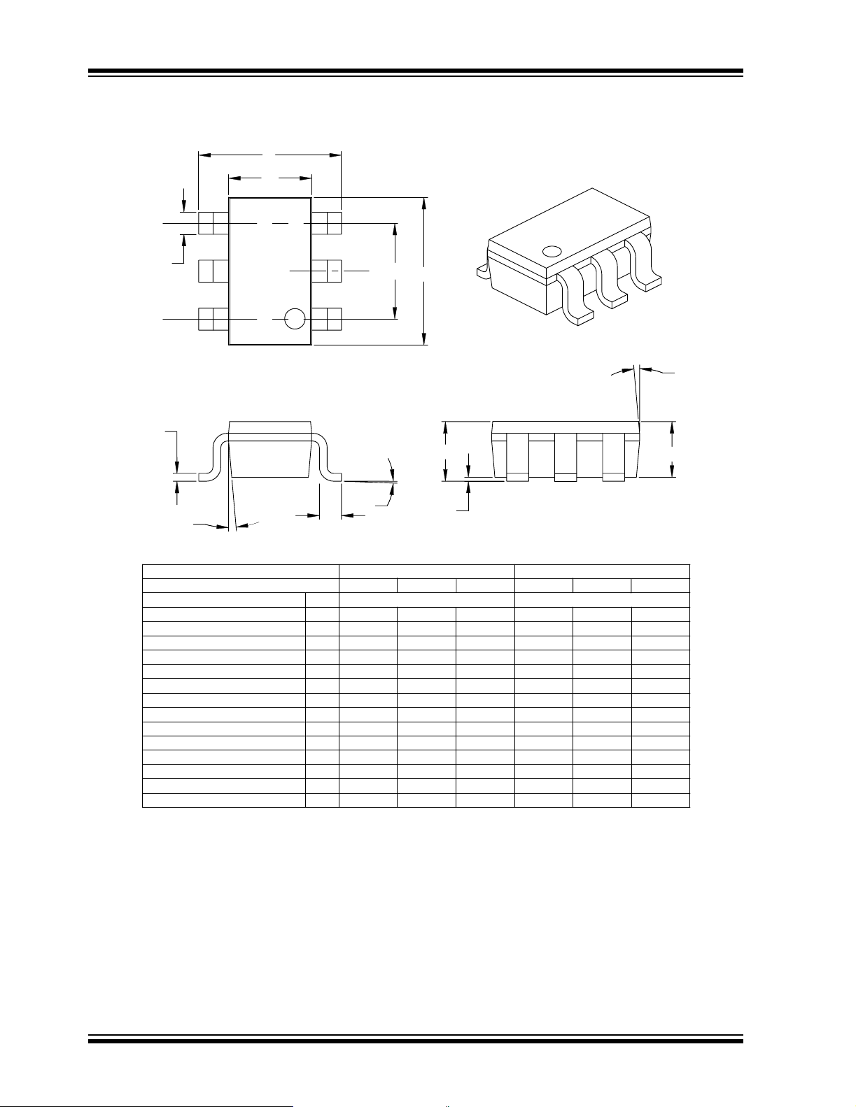
PIC10F220/222
6-Lead Plastic Small Outline Transistor (CH or OT) (SOT-23)
E
E1
B
n
c
β
Number of Pins
Pitch
Outside lead pitch (basic)
Molded Package Thickness
Standoff
erall Width
Molded Package Width
Foot Angle
Lead Thickness
Mold Draft Angle Top
Mold Draft Angle Bottom
*Controlling Parameter
Notes:
Dimensions D and E1 do not include mold flash or protrusions. Mold flash or protrusions shall not
exceed .005" (0.127mm) per side.
n
p
p1
A2
A1
E1
φ
c
α
β
p1
D
1
A
φ
NOM
A1
MINMAX
L
MINDimension Limits
α
A2
MILLIMETERSINCHES*Units
NOM
66
MAX
0.95.038
1.90.075
1.451.180.90.057.046.035AOverall Height
1.301.100.90.051.043.035
0.150.080.00.006.003.000
3.002.802.60.118.110.102EOv
1.751.631.50.069.064.059
3.102.952.80.122.116.110DOverall Length
0.550.450.35.022.018.014LFoot Length
10501050
0.200.150.09.008.006.004
0.500.430.35.020.017.014BLead Width
10501050
10501050
JEITA (formerly EIAJ) equivalent: SC-74A
Drawing No. C04-120
DS41270A-page 70 Preliminary © 2005 Microchip Technology Inc.
Page 71

-Lead Plastic Dual In-line (P) – 300 mil Body (PDIP)
E1
D
2
PIC10F220/222
n
E
β
eB
Number of Pins
Pitch
Top to Seating Plane A .140 .155 .170 3.56 3.94 4.32
Molded Package Thickness A2 .115 .130 .145 2.92 3.30 3.68
Base to Seating Plane A1 .015 0.38
Shoulder to Shoulder Width E .300 .313 .325 7.62 7.94 8.26
Molded Package Width E1 .240 .250 .260 6.10 6.35 6.60
Overall Length D .360 .373 .385 9.14 9.46 9.78
Tip to Seating Plane L .125 .130 .135 3.18 3.30 3.43
Lead Thickness
Upper Lead Width B1 .045 .058 .070 1.14 1.46 1.78
Lower Lead Width B .014 .018 .022 0.36 0.46 0.56
Overall Row Spacing § eB .310 .370 .430 7.87 9.40 10.92
Mold Draft Angle Top
Mold Draft Angle Bottom
* Controlling Parameter
§ Significant Characteristic
Notes:
Dimensions D and E1 do not include mold flash or protrusions. Mold flash or protrusions shall not exceed
.010” (0.254mm) per side.
JEDEC Equivalent: MS-001
Drawing No. C04-018
Dimension Limits MIN NOM MAX MIN NOM MAX
1
α
A
c
Units INCHES* MILLIMETERS
n
p
c
α
β
.008 .012 .015 0.20 0.29 0.38
A1
B1
B
88
.100 2.54
51015 51015
51015 51015
A2
L
p
© 2005 Microchip Technology Inc. Preliminary DS41270A-page 71
Page 72

PIC10F220/222
NOTES:
DS41270A-page 72 Preliminary © 2005 Microchip Technology Inc.
Page 73

INDEX
PIC10F220/222
A
ALU.....................................................................................11
Assembler
MPASM Assembler.....................................................64
B
Block Diagram
On-Chip Reset Circuit........................ ......................... 38
Timer0.........................................................................27
TMR0/WDT Prescaler.................................................30
Watchdog Timer..........................................................41
Brown-Out Protection Circuit ..............................................42
C
C Compilers
MPLAB C18...................... ..................... .....................64
MPLAB C30...................... ..................... .....................64
Carry...................................................................................11
Clocking Scheme................................................................13
Code Protection ............................................................35, 43
Configuration Bits................................................................35
Customer Change Notification Service ...............................75
Customer Notification Ser vice.............. ...............................75
Customer Support...............................................................75
D
DC and AC Characteristics.................................................67
Development Support .........................................................63
Digit Carry...........................................................................11
E
Errata....................................................................................5
F
Family of Devices
PIC10F22X...................................................................7
FSR ..................................................................................... 22
I
I/O Interfacing............ ..................... ..................... ...............23
I/O Ports..................... ..................... ....................................23
I/O Programming Considerations............. ..................... ......25
ID Locations..................................................................35, 43
INDF....................................................................................22
Indirect Data Addressing.....................................................22
Instruction Cycle .................................................................13
Instruction Flow/Pipelining ..................................................13
Instruction Set Summary.....................................................46
Internet Address.......................... ..................... ...................75
L
Loading of PC ........................................................... .... .. .. ..21
M
Memory Organization ......................................................... 15
Data Memory.............. .......................................... ...... 16
Program Memory (PIC10F220/222) ........................... 15
Microchip Internet Web Site................... ..................... ........ 75
MPLAB ASM30 Assembler, Li n ker, Librarian............... ...... 64
MPLAB ICD 2 In-Circuit Debugger ..................................... 65
MPLAB ICE 2000 High-Performance Universal
In-Circuit Emulator.............................................................. 65
MPLAB ICE 4000 High-Performance Universal
In-Circuit Emulator.............................................................. 65
MPLAB Integrated Development Environment Software.... 63
MPLAB PM3 Device Programmer...................................... 65
MPLINK Obje ct Linker/MPLIB Object Lib r a ri a n......... .. ....... 64
O
OPTION Register................................................................19
OSCCAL Register............................................... ................ 20
Oscillator Configurations.............. ....................................... 36
Oscillator Types
HS............................................................................... 36
LP............................................................................... 36
P
PIC10F220/222 Device Varieties.......................................... 9
PICSTART Plus Development Programmer....................... 66
POR
Device Reset Timer (DR T) ................................ .. . 3 5 , 4 0
............................................................................... 41
PD
Power-on Reset (POR)...............................................35
TO
............................................................................... 41
PORTB............................................................................... 23
Power-Down Mode............................................................. 42
Prescaler ............................................................................ 29
Program Counter................................................................ 21
Q
Q cycles................................................... ..................... ...... 13
R
Reader Response............................................................... 76
Read-Modify-Write.............................................................. 25
Register File Map
PIC10F220 ................................................................. 16
PIC10F222 ................................................................. 16
Registers
Special Function......................................................... 17
Reset.................................................................................. 35
Reset on Brown-Out........................................................... 42
S
Sleep ............................................................................ 35, 42
Software Simulator ( MP L AB SIM ).................... .................. 64
Special Features of the CPU.............................................. 35
Special Function Registers................................................. 17
Stack................................................................................... 21
STATUS Register................................................... 11, 18, 31
© 2005 Microchip Technology Inc. Preliminary DS41270A-page 73
Page 74

PIC10F220/222
T
Timer0
Timer0.........................................................................27
TMR0 with External Clock...........................................28
Timing Parameter Symbology and Load Conditions...........59
TMR0 ..................................................................................27
TRIS Registers....................................................... .............23
W
Wake-up from Sleep ...........................................................43
Watchdog Timer (WDT) ................................................35, 40
Period..........................................................................40
Programming Considerat io n s................................. ....40
WWW Address....................................................................75
WWW, On-Line Support........................................................5
Z
Zero bit............. ..................... ..................... ..................... ....11
DS41270A-page 74 Preliminary © 2005 Microchip Technology Inc.
Page 75

PIC10F220/222
THE MICROCHIP WEB SITE
Microchip provides onlin e support v ia our W WW site at
www.m ic roc hi p.c om . Thi s web si te i s us ed as a m ean s
to make files and information easily available to
customers. Accessible by using your favorite Internet
browser, the web site contains the following
information:
• Product Support – Data sheets and errata,
application notes and sample programs, design
resources, user’s guides and hardware support
documents, lat est softwa re releases and archived
software
• General Technical Support – Frequently Asked
Questions (FAQ), technical support requests,
online discussion groups, Microchip consultant
program member listing
• Business of Microchip – Product selector and
ordering guides, latest Microchip press releases,
listing of s eminars and events, listi ngs of
Microchip sales offices, distributors and factory
representatives
CUSTOMER CHANGE NOTIFICATION
SERVICE
CUSTOMER SUPPORT
Users of Microchip products can receive assistance
through several channels:
• Distributor or Representative
• Local Sal es Office
• Field Application Engineer (FAE)
• Technical Support
• Development Systems Information Line
Customers should contact their distributor,
representative or field application engineer (FAE) for
support. Local sales offices are also available to help
customers. A listing of sales offices and locations is
included in the back of this document.
T echnic al support is avail able throug h the web si te
at: http://support.microchip.com
Microchip’s customer notification service helps keep
customers current on Microchip products. Subscribers
will receive e-mail notification whenever there are
changes, updates, revisions or errata related to a
specified produ ct family or develo pment tool of inte rest.
To register, access the Microchip web site at
www.microchip.com, click on Customer Change
Notification and follow the registration instructions.
© 2005 Microchip Technology Inc. Preliminary DS41270A-page 75
Page 76

PIC10F220/222
READER RESPONSE
It is our intentio n to pro vi de you with the best documenta t ion po ss ib le to e ns ure successful use of your Microc hip product. If you wish to provid e your c omment s on org anizatio n, clarity, subject m atter, and ways in which o ur docum entatio n
can better serve you, please FAX your comments to the Technical Publications Manager at (480) 792-4150.
Please list the following information, and use this outline to provide us with your comments about this document.
To:
RE: Reader Response
From:
Application (optional):
Would you like a reply? Y N
Device: Literature Number:
Questions:
1. W hat are the best features of this document?
2. How does this document meet your hardware and software development needs?
3. Do you find the organization of this document easy to follow? If not, why?
Technical Publications Manager
Name
Company
Address
City / State / ZIP / Country
Telephone: (_______) _________ - _________
Total Pages Sent ________
FAX: (______) _________ - _________
DS41270APIC10F220/222
4. What additions to the document do you think would enhance the structure and subject?
5. What deletions from the document could be made without affecting the overall usefulness?
6. Is there any incorrect or misleading information (what and where)?
7. How would you improve this document?
DS41270A-page 76 Preliminary © 2005 Microchip Technology Inc.
Page 77

PIC10F220/222
PRODUCT IDENTIFICATION SYSTEM
To order or obtain information, e.g., on pricing or delivery, refer to the factory or the listed sales office.
PART NO. X /XX XXX
Device
Range
Device PIC10F220
(1)
, PIC10F222
PatternPackageTemperature
(1)
; VDD range 2.0V to 5.5V
Examples:
a) PIC10F220 - I/P = Industrial temp., PDIP
package (Pb-free)
b) PIC10F222 - T-I/OT = Industrial temp., SOT
package (Pb-free)
Temperature Range I = -40°C to +85°C (Industrial)
Package OT = SOT, 6-LD (Pb-free)
Pattern Special Requirements
E= -40°C to +125°C (Extended)
P = 300 mil PDIP, 8-LD (Pb-free)
Note 1: SOT packages are only available in tape
and reel.
© 2005 Microchip Technology Inc. Preliminary DS41270A-page 77
Page 78

WORLDWIDE SALES AND SERVICE
AMERICAS
Corporate Office
2355 West Chandler Blvd.
Chandler, AZ 85224-6199
Tel: 480-792-7200
Fax: 480-792-7277
Technical Support:
http://support.microchip.com
Web Address:
www.microchip.com
Atlanta
Alpharetta, GA
Tel: 770-640-0034
Fax: 770-640-0307
Boston
Westborough, MA
Tel: 774-760-0087
Fax: 774-760-0088
Chicago
Itasca, IL
Tel: 630-285-0071
Fax: 630-285-0075
Dallas
Addison, TX
Tel: 972-818-7423
Fax: 972-818-2924
Detroit
Farmington Hills, MI
Tel: 248-538-2250
Fax: 248-538-2260
Kokomo
Kokomo, IN
Tel: 765-864-8360
Fax: 765-864-8387
Los Angeles
Mission Viejo, CA
Tel: 949-462-9523
Fax: 949-462-9608
San Jose
Mountain View, CA
Tel: 650-215-1444
Fax: 650-961-0286
Toronto
Mississauga, Ontario,
Canada
Tel: 905-673-0699
Fax: 905-673-6509
ASIA/PACIFIC
Australia - Sydney
Tel: 61-2-9868-6733
Fax: 61-2-9868-6755
China - Beijing
Tel: 86-10-8528-2100
Fax: 86-10-8528-2104
China - Chengdu
Tel: 86-28-8676-6200
Fax: 86-28-8676-6599
China - Fuzhou
Tel: 86-591-8750-3506
Fax: 86-591-8750-3521
China - Hong Kong SAR
Tel: 852-2401-1200
Fax: 852-2401-3431
China - Qingdao
Tel: 86-532-502-7355
Fax: 86-532-502-7205
China - Shanghai
Tel: 86-21-5407-5533
Fax: 86-21-5407-5066
China - Shenyang
Tel: 86-24-2334-2829
Fax: 86-24-2334-2393
China - Shenzhen
Tel: 86-755-8203-2660
Fax: 86-755-8203-1760
China - Shunde
Tel: 86-757-2839-5507
Fax: 86-757-2839-5571
China - Wuhan
Tel: 86-27-5980-5300
Fax: 86-27-5980-5118
China - Xian
Tel: 86-29-8833-7250
Fax: 86-29-8833-7256
ASIA/PACIFIC
India - Bangalore
Tel: 91-80-2229-0061
Fax: 91-80-2229-0062
India - New Delhi
Tel: 91-11-5160-8631
Fax: 91-11-5160-8632
India - Pune
Tel: 91-20-2566-1512
Fax: 91-20-2566-1513
Japan - Yokohama
Tel: 81-45-471- 6166
Fax: 81-45-471-6122
Korea - Seoul
Tel: 82-2-554-7200
Fax: 82-2-558-5932 or
82-2-558-5934
Malaysia - Penang
Tel: 604-646-8870
Fax: 604-646-5086
Philippines - Manila
Tel: 011-632-634-9065
Fax: 011-632-634-9069
Singapore
Tel: 65-6334-8870
Fax: 65-6334-8850
Taiwan - Hsinchu
Tel: 886-3-572-9526
Fax: 886-3-572-6459
Taiwan - Kaohsiung
Tel: 886-7-536-4818
Fax: 886-7-536-4803
Taiwan - Taipei
Tel: 886-2-2500-6610
Fax: 886-2-2508-0102
Thailand - Bangkok
Tel: 66-2-694-1351
Fax: 66-2-694-1350
EUROPE
Austria - Weis
Tel: 43-7242-2244-399
Fax: 43-7242-2244-393
Denmark - Copenhagen
Tel: 45-4450-2828
Fax: 45-4485-2829
France - Paris
Tel: 33-1-69-53-63-20
Fax: 33-1-69-30-90-79
Germany - Munich
Tel: 49-89-627-144-0
Fax: 49-89-627-144-44
Italy - Milan
Tel: 39-0331-742611
Fax: 39-0331-466781
Netherlands - Drunen
Tel: 31-416-690399
Fax: 31-416-690340
Spain - Madrid
Tel: 34-91-352-30-52
Fax: 34-91-352-11-47
UK - Wokingham
Tel: 44-118-921-5869
Fax: 44-118-921-5820
07/01/05
DS41270A-page 78 © 2005 Microchip Technology Inc.
 Loading...