


查询PIC10F206-E/MC供应商
PIC10F200/202/204/206
Data Sheet
6-Pin, 8-bit Flash Microcontrollers
© 2007 Microchip Technology Inc. DS41239D

Note the following details of the code protection feature on Microchip devices:
• Microchip products meet the specification contained in their particular Microchip Data Sheet.
• Microchip believes that its family of products is one of the most secure families of its kind on the market today, when used in the
intended manner and under normal conditions.
• There are dishonest and possibly illegal methods used to breach the code protection feature. All of these methods, to our
knowledge, require using the Microchip products in a manner outside the operating specifications contained in Microchip’s Data
Sheets. Most likely, the person doing so is engaged in theft of intellectual property.
• Microchip is willing to work with the customer who is concerned about the integrity of their code.
• Neither Microchip nor any other semiconductor manufacturer can guarantee the security of their code. Code protection does not
mean that we are guaranteeing the product as “unbreakable.”
Code protection is constantly evolving. We at Microchip are committed to continuously improving the code protection features of our
products. Attempts to break Microchip’s code protection feature may be a violation of the Digital Millennium Copyright Act. If such acts
allow unauthorized access to your software or other copyrighted work, you may have a right to sue for relief under that Act.
Information contained in this publication regarding device
applications and the like is provided only for your convenience
and may be superseded by updates. It is your responsibility to
ensure that your application meets with your specifications.
MICROCHIP MAKES NO REPRESENTATIONS OR
WARRANTIES OF ANY KIND WHETHER EXPRESS OR
IMPLIED, WRITTEN OR ORAL, STATUTORY OR
OTHERWISE, RELATED TO THE INFORMATION,
INCLUDING BUT NOT LIMITED TO ITS CONDITION,
QUALITY, PERFORMANCE, MERCHANTABILITY OR
FITNESS FOR PURPOSE. Microchip disclaims all liability
arising from this information and its use. Use of Microchip
devices in life support and/or safety applications is entirely at
the buyer’s risk, and the buyer agrees to defend, indemnify and
hold harmless Microchip from any and all damages, claims,
suits, or expenses resulting from such use. No licenses are
conveyed, implicitly or otherwise, under any Microchip
intellectual property rights.
Trademarks
The Microchip name and logo, the Microchip logo, Accuron,
dsPIC, K
EELOQ, KEELOQ logo, microID, MPLAB, PIC,
PICmicro, PICSTART, PRO MATE, PowerSmart, rfPIC, and
SmartShunt are registered trademarks of Microchip
Technology Incorporated in the U.S.A. and other countries.
AmpLab, FilterLab, Linear Active Thermistor, Migratable
Memory, MXDEV, MXLAB, PS logo, SEEVAL, SmartSensor
and The Embedded Control Solutions Company are
registered trademarks of Microchip Technology Incorporated
in the U.S.A.
Analog-for-the-Digital Age, Application Maestro, CodeGuard,
dsPICDEM, dsPICDEM.net, dsPICworks, ECAN,
ECONOMONITOR, FanSense, FlexROM, fuzzyLAB,
In-Circuit Serial Programming, ICSP, ICEPIC, Mindi, MiWi,
MPASM, MPLAB Certified logo, MPLIB, MPLINK, PICkit,
PICDEM, PICDEM.net, PICLAB, PICtail, PowerCal,
PowerInfo, PowerMate, PowerTool, REAL ICE, rfLAB,
rfPICDEM, Select Mode, Smart Serial, SmartTel, Total
Endurance, UNI/O, WiperLock and ZENA are trademarks of
Microchip Technology Incorporated in the U.S.A. and other
countries.
SQTP is a service mark of Microchip Technology Incorporated
in the U.S.A.
All other trademarks mentioned herein are property of their
respective companies.
© 2007, Microchip Technology Incorporated, Printed in the
U.S.A., All Rights Reserved.
Printed on recycled paper.
Microchip received ISO/TS-16949:2002 certification for its worldwide
headquarters, design and wafer fabrication facilities in Chandler and
Tempe, Arizona, Gresham, Oregon and Mountain View, California. The
Company’s quality system processes and procedures are for its PIC
MCUs and dsPIC® DSCs, KEELOQ
EEPROMs, microperipherals, nonvolatile memory and analog
products. In addition, Microchip’s quality system for the design and
manufacture of development systems is ISO 9001:2000 certified.
®
code hopping devices, Serial
DS41239D-page ii © 2007 Microchip Technology Inc.
®

PIC10F200/202/204/206
6-Pin, 8-Bit Flash Microcontrollers
Devices Included In This Data Sheet:
• PIC10F200 • PIC10F204
• PIC10F202 • PIC10F206
High-Performance RISC CPU:
• Only 33 single-word instructions to learn
• All single-cycle instructions except for program
branches, which are two-cycle
• 12-bit wide instructions
• 2-level deep hardware stack
• Direct, Indirect and Relative Addressing modes
for data and instructions
• 8-bit wide data path
• 8 Special Function Hardware registers
• Operating speed:
- 4 MHz internal clock
-1μs instruction cycle
Special Microcontroller Features:
• 4 MHz precision internal oscillator:
- Factory calibrated to ±1%
• In-Circuit Serial Programming™ (ICSP™)
• In-Circuit Debugging (ICD) support
• Power-on Reset (POR)
• Device Reset Timer (DRT)
• Watchdog Timer (WDT) with dedicated on-chip
RC oscillator for reliable operation
• Programmable code protection
• Multiplexed MCLR
• Internal weak pull-ups on I/O pins
• Power-Saving Sleep mode
• Wake-up from Sleep on pin change
input pin
Low-Power Features/CMOS Technology:
• Operating Current:
- < 175 μA @ 2V, 4 MHz, typical
• Standby Current:
- 100 nA @ 2V, typical
• Low-power, high-speed Flash technology:
- 100,000 Flash endurance
- > 40 year retention
• Fully static design
• Wide operating voltage range: 2.0V to 5.5V
• Wide temperature range:
- Industrial: -40°C to +85°C
- Extended: -40°C to +125°C
Peripheral Features (PIC10F200/202):
• 4 I/O pins:
- 3 I/O pins with individual direction control
- 1 input-only pin
- High current sink/source for direct LED drive
- Wake-on-change
- Weak pull-ups
• 8-bit real-time clock/counter (TMR0) with 8-bit
programmable prescaler
Peripheral Features (PIC10F204/206):
• 4 I/O pins:
- 3 I/O pins with individual direction control
- 1 input-only pin
- High current sink/source for direct LED drive
- Wake-on-change
- Weak pull-ups
• 8-bit real-time clock/counter (TMR0) with 8-bit
programmable prescaler
• 1 Comparator:
- Internal absolute voltage reference
- Both comparator inputs visible externally
- Comparator output visible externally
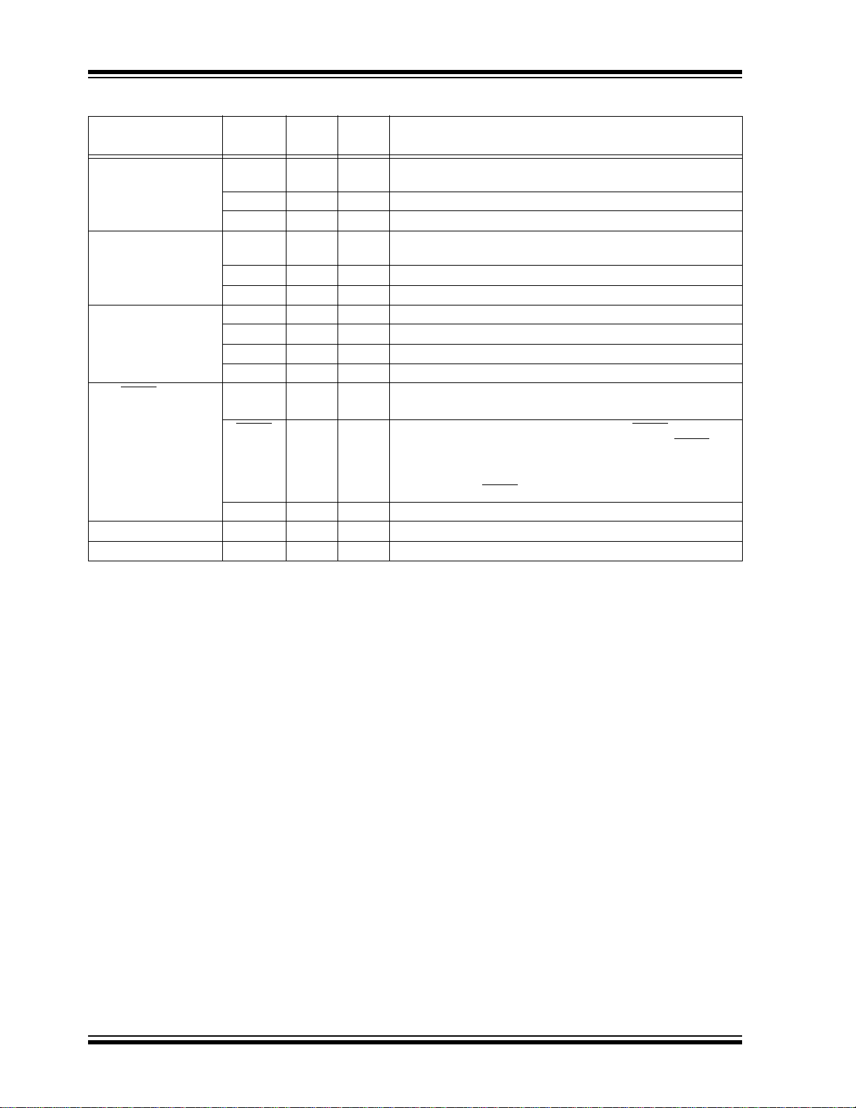
TABLE 1-1: PIC10F20X MEMORY AND FEATURES
Device
PIC10F200 256 16 4 1 0
PIC10F202 512 24 4 1 0
PIC10F204 256 16 4 1 1
PIC10F206 512 24 4 1 1
© 2007 Microchip Technology Inc. DS41239D-page 1
Program Memory Data Memory
I/O
Flash (words) SRAM (bytes)
Timers
8-bit
Comparator
PIC10F200/202/204/206
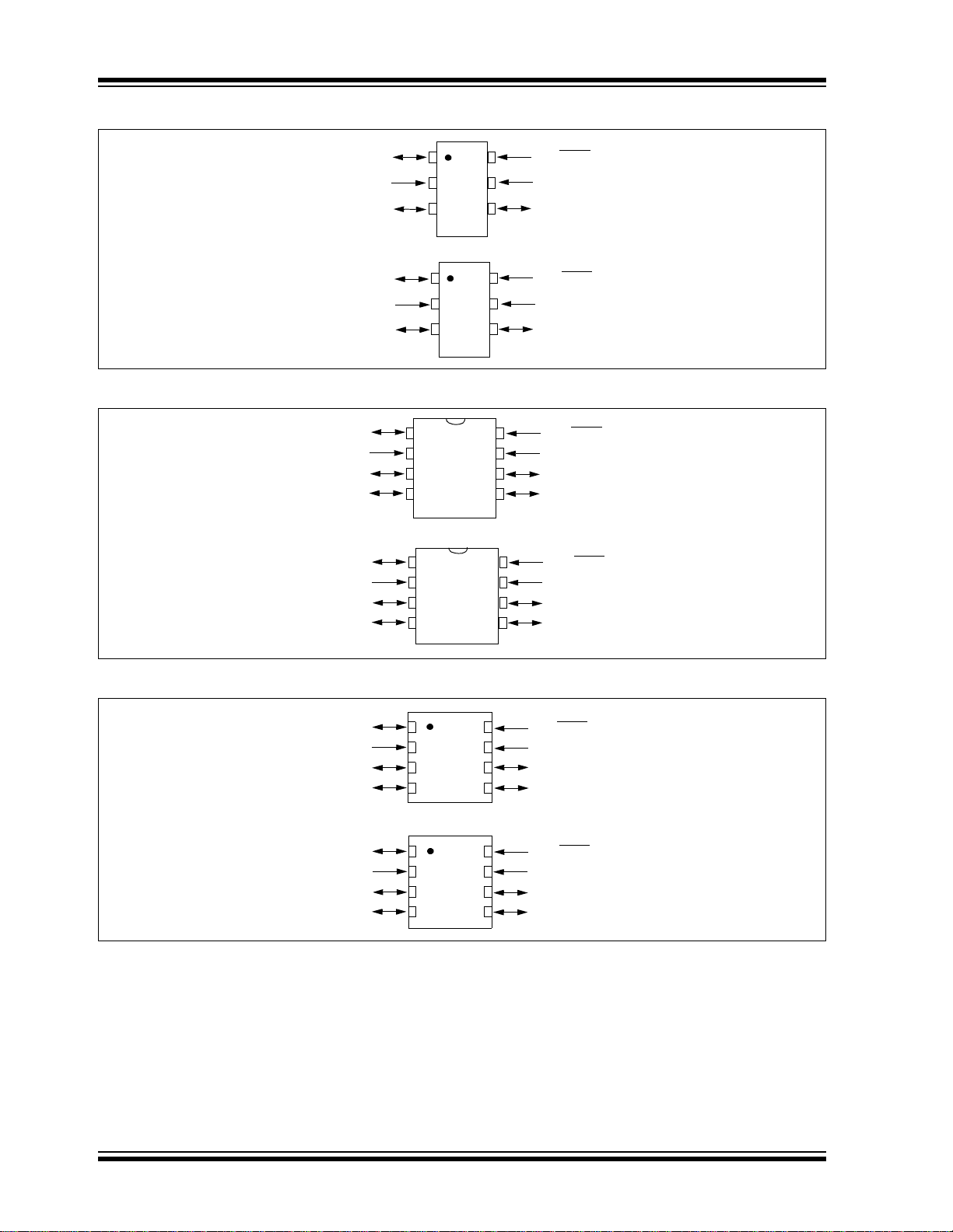
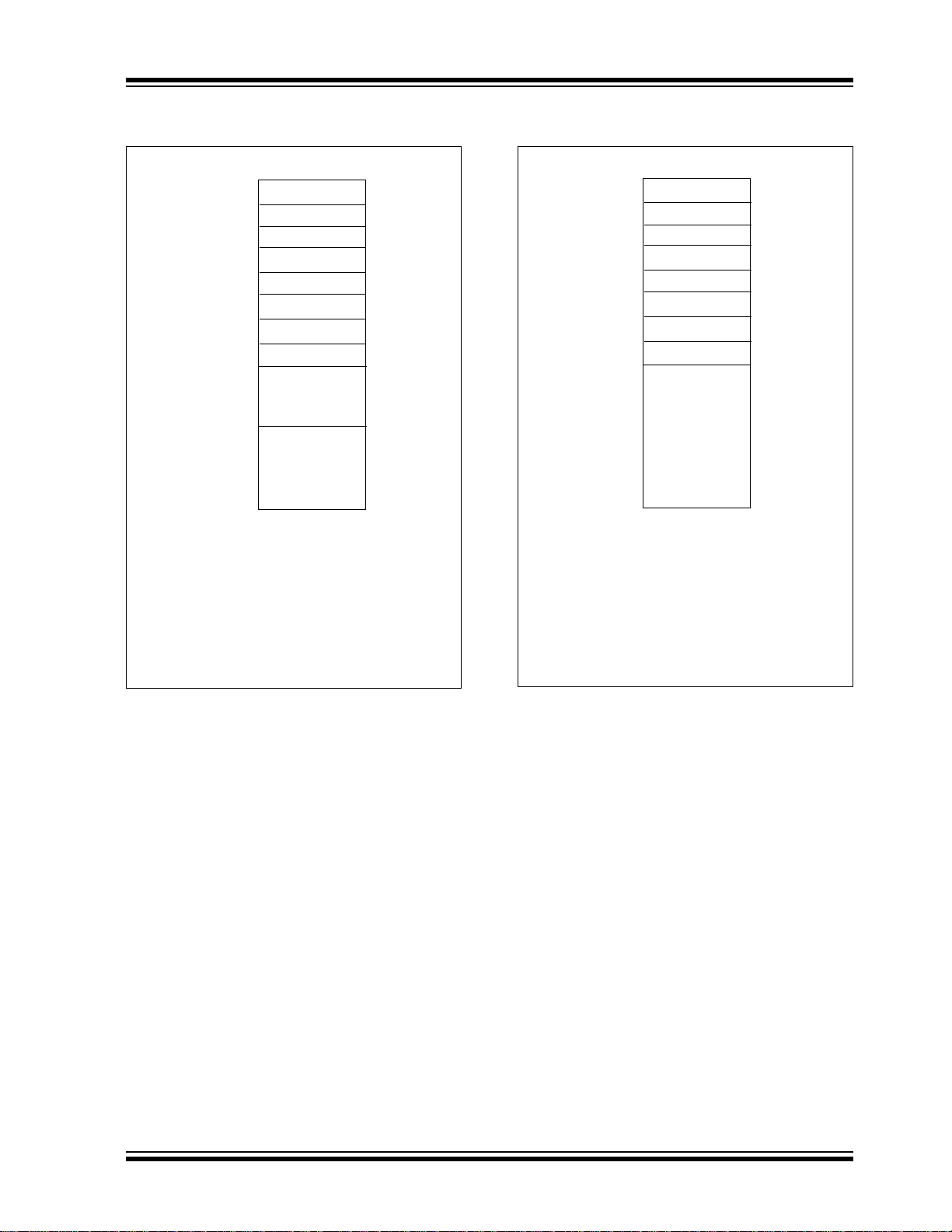
SOT-23 Pin Diagrams
8-Pin PDIP Pin Diagrams
GP2/T0CKI/FOSC4
GP2/T0CKI/COUT/FOSC4
GP1/ICSPCLK/CIN-
GP0/ICSPDAT
V
SS
GP1/ICSPCLK
GP0/ICSPDAT/CIN+
V
GP1/ICSPCLK/CIN-
N/C
VDD
GP1/ICSPCLK
N/C
VDD
6
1
5
2
4
3
PIC10F200/202
1
6
SS
2
5
3
4
PIC10F204/206
1
2
3
4
1
2
3
4
8
7
6
5
PIC10F200/202
PIC10F204/206
GP3/MCLR
VDD
GP2/T0CKI/FOSC4
GP3/MCLR
VDD
GP2/T0CKI/COUT/FOSC4
8
7
6
5
/VPP
/VPP
GP3/MCLR/VPP
VSS
N/C
GP0/ICSPDAT
GP3/MCLR/VPP
VSS
N/C
GP0/ICSPDAT/CIN+
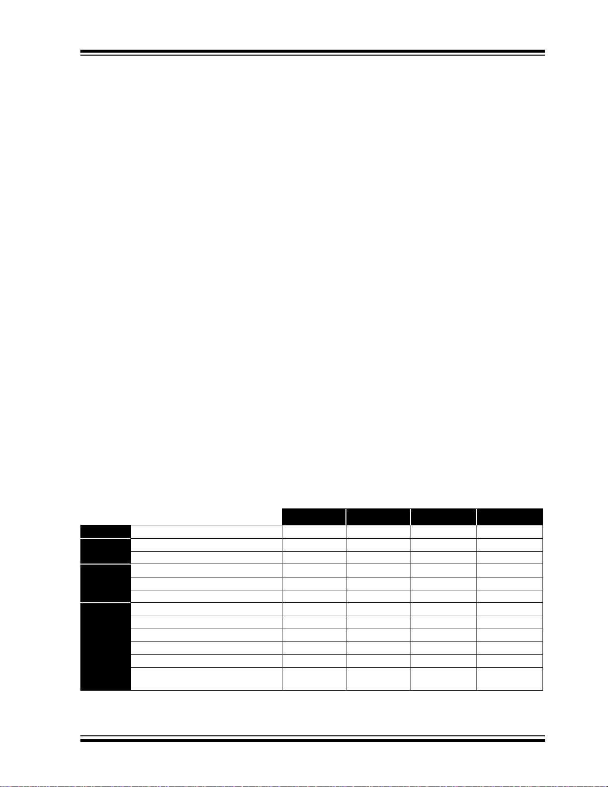
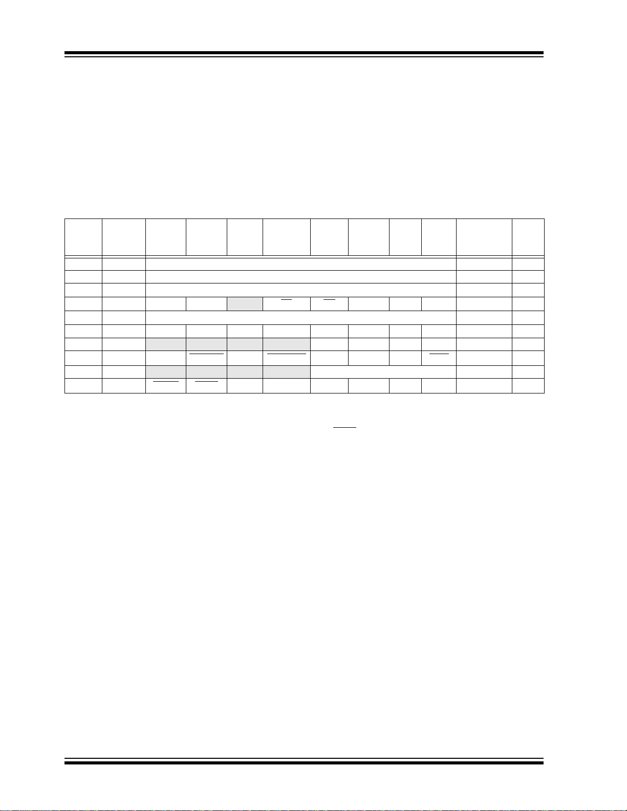
8-Pin DFN Pin Diagrams
GP2/T0CKI/FOSC4
GP2/T0CKI/COUT/FOSC4
GP1/ICSPCLK/CIN-
N/C
VDD
GP1/ICSPCLK
N/C
VDD
PIC10F200/202
PIC10F204/206
8
7
6
5
8
7
6
5
GP3/MCLR/VPP
VSS
N/C
GP0/ICSPDAT
GP3/MCLR/VPP
VSS
N/C
GP0/ICSPDAT/CIN+
1
2
3
4
1
2
3
4
DS41239D-page 2 © 2007 Microchip Technology Inc.

PIC10F200/202/204/206
Table of Contents
1.0 General Description...................................................................................................................................................................... 5
2.0 PIC10F200/202/204/206 Device Varieties .................................................................................................................................. 7
3.0 Architectural Overview ................................................................................................................................................................. 9
4.0 Memory Organization ................................................................................................................................................................. 15
5.0 I/O Port....................................................................................................................................................................................... 25
6.0 Timer0 Module and TMR0 Register (PIC10F200/202)............................................................................................................... 29
7.0 Timer0 Module and TMR0 Register (PIC10F204/206)............................................................................................................... 33
8.0 Comparator Module.................................................................................................................................................................... 37
9.0 Special Features of the CPU...................................................................................................................................................... 41
10.0 Instruction Set Summary............................................................................................................................................................ 51
11.0 Development Support................................................................................................................................................................. 59
12.0 Electrical Characteristics............................................................................................................................................................ 63
13.0 DC and AC Characteristics Graphs and Tables......................................................................................................................... 73
14.0 Packaging Information................................................................................................................................................................ 81
Index .................................................................................................................................................................................................... 89
The Microchip Web Site....................................................................................................................................................................... 91
Customer Change Notification Service ................................................................................................................................................ 91
Customer Support ................................................................................................................................................................................ 91
Reader Response ................................................................................................................................................................................ 92
Product Identification System .............................................................................................................................................................. 93
TO OUR VALUED CUSTOMERS
It is our intention to provide our valued customers with the best documentation possible to ensure successful use of your Microchip products. To this end, we will continue to improve our publications to better suit your needs. Our publications will be refined
and enhanced as new volumes and updates are introduced.
If you have any questions or comments regarding this publication, please contact the Marketing Communications Department via
E-mail at docerrors@mail.microchip.com or fax the Reader Response Form in the back of this data sheet to (480) 792-4150.
We welcome your feedback.
Most Current Data Sheet
To obtain the most up-to-date version of this data sheet, please register at our Worldwide Web site at:
http://www.microchip.com
You can determine the version of a data sheet by examining its literature number found on the bottom outside corner of any page.
The last character of the literature number is the version number, (e.g., DS30000A is version A of document DS30000).
Errata
An errata sheet, describing minor operational differences from the data sheet and recommended workarounds, may exist for current
devices. As device/documentation issues become known to us, we will publish an errata sheet. The errata will specify the revision
of silicon and revision of document to which it applies.
To determine if an errata sheet exists for a particular device, please check with one of the following:
• Microchip’s Worldwide Web site; http://www.microchip.com
• Your local Microchip sales office (see last page)
• The Microchip Corporate Literature Center; U.S. FAX: (480) 792-7277
When contacting a sales office or the literature center, please specify which device, revision of silicon and data sheet (include lit-
erature number) you are using.
Customer Notification System
Register on our web site at www.microchip.com/cn to receive the most current information on all of our products.
© 2007 Microchip Technology Inc. DS41239D-page 3

PIC10F200/202/204/206
NOTES:
DS41239D-page 4 © 2007 Microchip Technology Inc.
PIC10F200/202/204/206
1.0 GENERAL DESCRIPTION
The PIC10F200/202/204/206 devices from Microchip
Technology are low-cost, high-performance, 8-bit, fullystatic, Flash-based CMOS microcontrollers. They
employ a RISC architecture with only 33 single-word/
single-cycle instructions. All instructions are single
cycle (1 μs) except for program branches, which take
two cycles. The PIC10F200/202/204/206 devices
deliver performance in an order of magnitude higher
than their competitors in the same price category. The
12-bit wide instructions are highly symmetrical, resulting in a typical 2:1 code compression over other 8-bit
microcontrollers in its class. The easy-to-use and easy
to remember instruction set reduces development time
significantly.
The PIC10F200/202/204/206 products are equipped
with special features that reduce system cost and
power requirements. The Power-on Reset (POR) and
Device Reset Timer (DRT) eliminate the need for external Reset circuitry. INTRC Internal Oscillator mode is
provided, thereby preserving the limited number of I/O
available. Power-Saving Sleep mode, Watchdog Timer
and code protection features improve system cost,
power and reliability.
The PIC10F200/202/204/206 devices are available in
cost-effective Flash, which is suitable for production in
any volume. The customer can take full advantage of
Microchip’s price leadership in Flash programmable
microcontrollers, while benefiting from the Flash
programmable flexibility.
The PIC10F200/202/204/206 products are supported
by a full-featured macro assembler, a software simulator, an in-circuit debugger, a ‘C’ compiler, a low-cost
development programmer and a full featured programmer. All the tools are supported on IBM
compatible machines.
®
PC and
1.1 Applications
The PIC10F200/202/204/206 devices fit in applications
ranging from personal care appliances and security
systems to low-power remote transmitters/receivers.
The Flash technology makes customizing application
programs (transmitter codes, appliance settings,
receiver frequencies, etc.) extremely fast and convenient. The small footprint packages, for through hole or
surface mounting, make these microcontrollers well
suited for applications with space limitations. Low cost,
low power, high performance, ease-of-use and I/O
flexibility make the PIC10F200/202/204/206 devices
very versatile even in areas where no microcontroller
use has been considered before (e.g., timer functions,
logic and PLDs in larger systems and coprocessor
applications).
TABLE 1-1: PIC10F200/202/204/206 DEVICES
PIC10F200 PIC10F202 PIC10F204 PIC10F206
Clock Maximum Frequency of Operation (MHz) 4 4 4 4
Memory Flash Program Memory 256 512 256 512
Data Memory (bytes) 16 24 16 24
Peripherals Timer Module(s) TMR0 TMR0 TMR0 TMR0
Wake-up from Sleep on Pin Change Yes Yes Yes Yes
Comparators 0 0 1 1
Features I/O Pins 3 3 3 3
Input-Only Pins 1 1 1 1
Internal Pull-ups Yes Yes Yes Yes
In-Circuit Serial Programming™ Yes Yes Yes Yes
Number of Instructions 33 33 33 33
Packages 6-pin SOT-23
8-pin PDIP, DFN
The PIC10F200/202/204/206 devices have Power-on Reset, selectable Watchdog Timer, selectable code-protect, high I/O current
capability and precision internal oscillator.
The PIC10F200/202/204/206 device uses serial programming with data pin GP0 and clock pin GP1.
© 2007 Microchip Technology Inc. DS41239D-page 5
6-pin SOT-23
8-pin PDIP, DFN
6-pin SOT-23
8-pin PDIP, DFN
6-pin SOT-23
8-pin PDIP, DFN

PIC10F200/202/204/206
NOTES:
DS41239D-page 6 © 2007 Microchip Technology Inc.

PIC10F200/202/204/206
2.0 PIC10F200/202/204/206 DEVICE
VARIETIES
A variety of packaging options are available. Depending on application and production requirements, the
proper device option can be selected using the
information in this section. When placing orders, please
use the PIC10F200/202/204/206 Product Identification
System at the back of this data sheet to specify the
correct part number.
2.1 Quick Turn Programming (QTP)
Devices
Microchip offers a QTP programming service for
factory production orders. This service is made
available for users who choose not to program
medium-to-high quantity units and whose code
patterns have stabilized. The devices are identical to
the Flash devices but with all Flash locations and fuse
options already programmed by the factory. Certain
code and prototype verification procedures do apply
before production shipments are available. Please
contact your local Microchip Technology sales office for
more details.
2.2 Serialized Quick Turn
Programming
Microchip offers a unique programming service, where
a few user-defined locations in each device are
programmed with different serial numbers. The serial
numbers may be random, pseudo-random or
sequential.
Serial programming allows each device to have a
unique number, which can serve as an entry code,
password or ID number.
SM
(SQTPSM) Devices
© 2007 Microchip Technology Inc. DS41239D-page 7

PIC10F200/202/204/206
NOTES:
DS41239D-page 8 © 2007 Microchip Technology Inc.

PIC10F200/202/204/206
3.0 ARCHITECTURAL OVERVIEW
The high performance of the PIC10F200/202/204/206
devices can be attributed to a number of architectural
features commonly found in RISC microprocessors. To
begin with, the PIC10F200/202/204/206 devices use a
Harvard architecture in which program and data are
accessed on separate buses. This improves bandwidth over traditional von Neumann architectures
where program and data are fetched on the same bus.
Separating program and data memory further allows
instructions to be sized differently than the 8-bit wide
data word. Instruction opcodes are 12 bits wide,
making it possible to have all single-word instructions.
A 12-bit wide program memory access bus fetches a
12-bit instruction in a single cycle. A two-stage pipeline
overlaps fetch and execution of instructions.
Consequently, all instructions (33) execute in a single
cycle (1 μs @ 4 MHz) except for program branches.
The table below lists program memory (Flash) and data
memory (RAM) for the PIC10F200/202/204/206
devices.
TABLE 3-1: PIC10F2XX MEMORY
Memory
Device
Program Data
PIC10F200 256 x 12 16 x 8
PIC10F202 512 x 12 24 x 8
PIC10F204 256 x 12 16 x 8
PIC10F206 512 x 12 24 x 8
The PIC10F200/202/204/206 devices contain an 8-bit
ALU and working register. The ALU is a general
purpose arithmetic unit. It performs arithmetic and
Boolean functions between data in the working register
and any register file.
The ALU is 8 bits wide and capable of addition, subtraction, shift and logical operations. Unless otherwise
mentioned, arithmetic operations are two’s complement in nature. In two-operand instructions, one operand is typically the W (working) register. The other
operand is either a file register or an immediate constant. In single operand instructions, the operand is
either the W register or a file register.
The W register is an 8-bit working register used for ALU
operations. It is not an addressable register.
Depending on the instruction executed, the ALU may
affect the values of the Carry (C), Digit Carry (DC) and
Zero (Z) bits in the STATUS register. The C and DC bits
operate as a borrow
tively, in subtraction. See the SUBWF and ADDWF
instructions for examples.
A simplified block diagram is shown in Figure 3-1 and
Figure 3-2, with the corresponding device pins
described in Table 3-2.
and digit borrow out bit, respec-
The PIC10F200/202/204/206 devices can directly or
indirectly address its register files and data memory. All
Special Function Registers (SFR), including the PC,
are mapped in the data memory. The PIC10F200/202/
204/206 devices have a highly orthogonal
(symmetrical) instruction set that makes it possible to
carry out any operation, on any register, using any
addressing mode. This symmetrical nature and lack of
“special optimal situations” make programming with the
PIC10F200/202/204/206 devices simple, yet efficient.
In addition, the learning curve is reduced significantly.
© 2007 Microchip Technology Inc. DS41239D-page 9
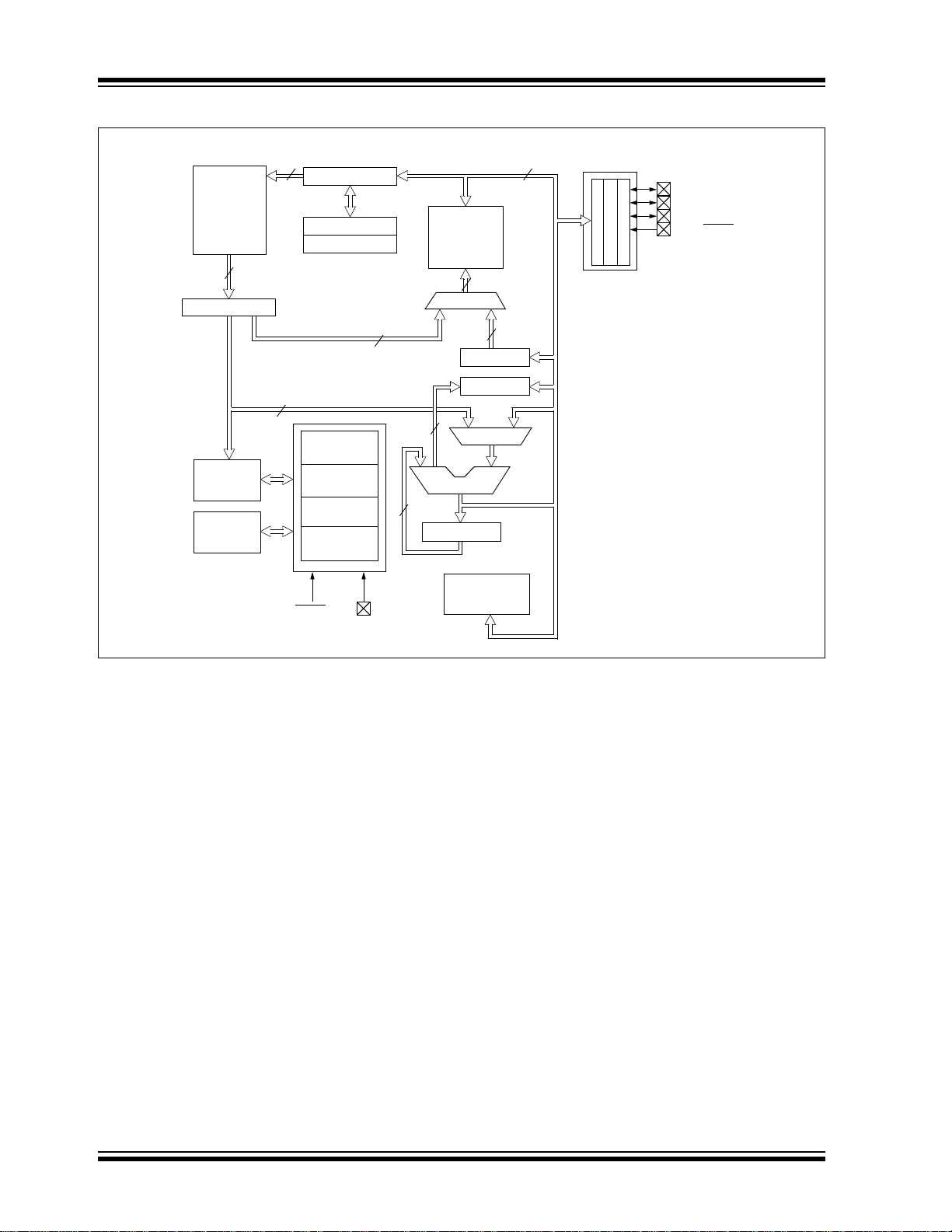
PIC10F200/202/204/206
FIGURE 3-1: PIC10F200/202 BLOCK DIAGRAM
Program
Bus
Flash
512 x12 or
256 x12
Program
Memory
12
Instruction Reg
Instruction
Decode &
Control
Timing
Generation
9-10
Program Counter
Direct Addr
8
Device Reset
Power-on
Watchdog
Internal RC
MCLR
Stack 1
Stack 2
Timer
Reset
Timer
Clock
VDD, VSS
RAM Addr
5
Data Bus
RAM
24 or 16
bytes
File
Registers
Addr MUX
3
ALU
8
W Reg
9
Indirect
5-7
Addr
FSR Reg
STATUS Reg
MUX
Timer0
8
GPIO
GP0/ICSPDAT
GP1/ICSPCLK
GP2/T0CKI/FOSC4
GP3/MCLR/VPP
DS41239D-page 10 © 2007 Microchip Technology Inc.
PIC10F200/202/204/206
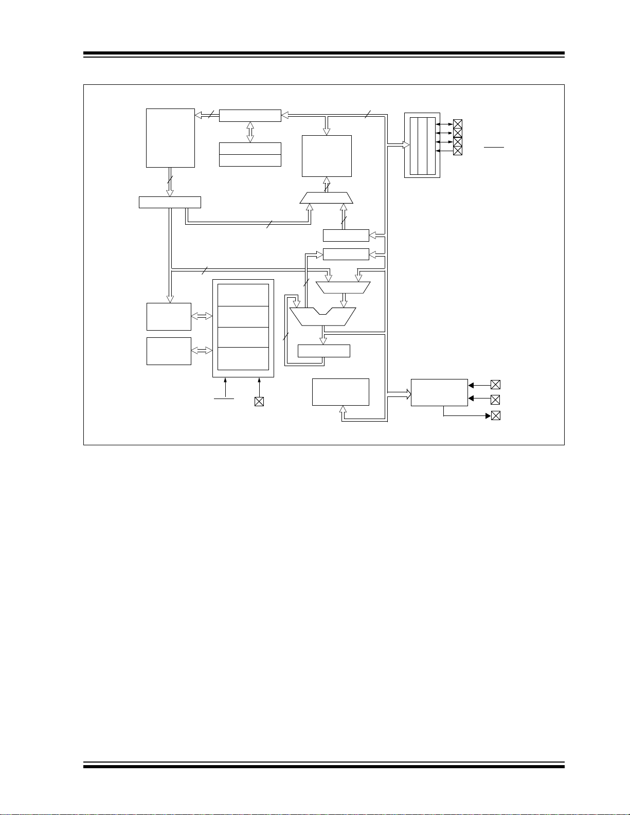
FIGURE 3-2: PIC10F204/206 BLOCK DIAGRAM
Program
Bus
Flash
512 x12 or
256 x12
Program
Memory
12
Instruction Reg
Instruction
Decode &
Control
Timing
Generation
9-10
Program Counter
Direct Addr
8
Device Reset
Power-on
Watchdog
Internal RC
MCLR
Stack 1
Stack 2
Timer
Reset
Timer
Clock
VDD, VSS
RAM Addr
5
Data Bus
RAM
24 or 16
bytes
File
Registers
Addr MUX
3
ALU
8
W Reg
9
Indirect
5-7
Addr
FSR Reg
STATUS Reg
MUX
Timer0
8
GPIO
Comparator
GP0/ICSPDAT/CIN+
GP1/ICSPCLK/CINGP2/T0CKI/COUT/FOSC4
GP3/MCLR/VPP
CIN+
CIN-
COUT
© 2007 Microchip Technology Inc. DS41239D-page 11
PIC10F200/202/204/206
TABLE 3-2: PIC10F200/202/204/206 PINOUT DESCRIPTION
Name Function
GP0/ICSPDAT/CIN+ GP0 TTL CMOS Bidirectional I/O pin. Can be software programmed for internal
ICSPDAT ST CMOS In-Circuit Serial Programming
CIN+ AN — Comparator input (PIC10F204/206 only).
GP1/ICSPCLK/CIN- GP1 TTL CMOS Bidirectional I/O pin. Can be software programmed for internal
ICSPCLK ST CMOS In-Circuit Serial Programming clock pin.
CIN- AN — Comparator input (PIC10F204/206 only).
GP2/T0CKI/COUT/
FOSC4
GP3/MCLR
VDD VDD P — Positive supply for logic and I/O pins.
SS VSS P — Ground reference for logic and I/O pins.
V
Legend: I = Input, O = Output, I/O = Input/Output, P = Power, — = Not used, TTL = TTL input,
/VPP GP3 TTL — Input pin. Can be software programmed for internal weak
ST = Schmitt Trigger input, AN = Analog input
GP2 TTL CMOS Bidirectional I/O pin.
T0CKI ST — Clock input to TMR0.
COUT — CMOS Comparator output (PIC10F204/206 only).
FOSC4 — CMOS Oscillator/4 output.
MCLR
VPP HV — Programming voltage input.
Input
Type
Output
Typ e
weak pull-up and wake-up from Sleep on pin change.
weak pull-up and wake-up from Sleep on pin change.
pull-up and wake-up from Sleep on pin change.
ST — Master Clear (Reset). When configured as MCLR, this pin is
an active-low Reset to the device. Voltage on GP3/MCLR
must not exceed V
device will enter Programming mode. Weak pull-up always on
if configured as MCLR.
Description
™
data pin.
/VPP
DD during normal device operation or the
DS41239D-page 12 © 2007 Microchip Technology Inc.
PIC10F200/202/204/206
3.1 Clocking Scheme/Instruction
Cycle
The clock is internally divided by four to generate four
non-overlapping quadrature clocks, namely Q1, Q2,
Q3 and Q4. Internally, the PC is incremented every Q1
and the instruction is fetched from program memory
and latched into the instruction register in Q4. It is
decoded and executed during the following Q1 through
Q4. The clocks and instruction execution flow is shown
in Figure 3-3 and Example 3-1.
FIGURE 3-3: CLOCK/INSTRUCTION CYCLE
Q2 Q3 Q4
Q1
OSC1
Q1
Q2
Q3
Q4
PC PC PC + 1 PC + 2
Q1
3.2 Instruction Flow/Pipelining
An instruction cycle consists of four Q cycles (Q1, Q2,
Q3 and Q4). The instruction fetch and execute are
pipelined such that fetch takes one instruction cycle,
while decode and execute take another instruction
cycle. However, due to the pipelining, each instruction
effectively executes in one cycle. If an instruction
causes the PC to change (e.g., GOTO), then two cycles
are required to complete the instruction (Example 3-1).
A fetch cycle begins with the PC incrementing in Q1.
In the execution cycle, the fetched instruction is latched
into the Instruction Register (IR) in cycle Q1. This
instruction is then decoded and executed during the
Q2, Q3 and Q4 cycles. Data memory is read during Q2
(operand read) and written during Q4 (destination
write).
Q2 Q3 Q4
Q1
Q2 Q3 Q4
Internal
phase
clock
Fetch INST (PC)
Execute INST (PC – 1)
Fetch INST (PC + 1)
Execute INST (PC)
Fetch INST (PC + 2)
Execute INST (PC + 1)
EXAMPLE 3-1: INSTRUCTION PIPELINE FLOW
1. MOVLW 03H
2. MOVWF GPIO
3. CALL SUB_1
4. BSF GPIO, BIT1
All instructions are single cycle, except for any program branches. These take two cycles, since the fetch instruction
is “flushed” from the pipeline, while the new instruction is being fetched and then executed.
Fetch 1 Execute 1
Fetch 2 Execute 2
Fetch 3 Execute 3
Fetch 4 Flush
Fetch SUB_1 Execute SUB_1
© 2007 Microchip Technology Inc. DS41239D-page 13

PIC10F200/202/204/206
NOTES:
DS41239D-page 14 © 2007 Microchip Technology Inc.
PIC10F200/202/204/206
4.0 MEMORY ORGANIZATION
The PIC10F200/202/204/206 memories are organized
into program memory and data memory. Data memory
banks are accessed using the File Select Register
(FSR).
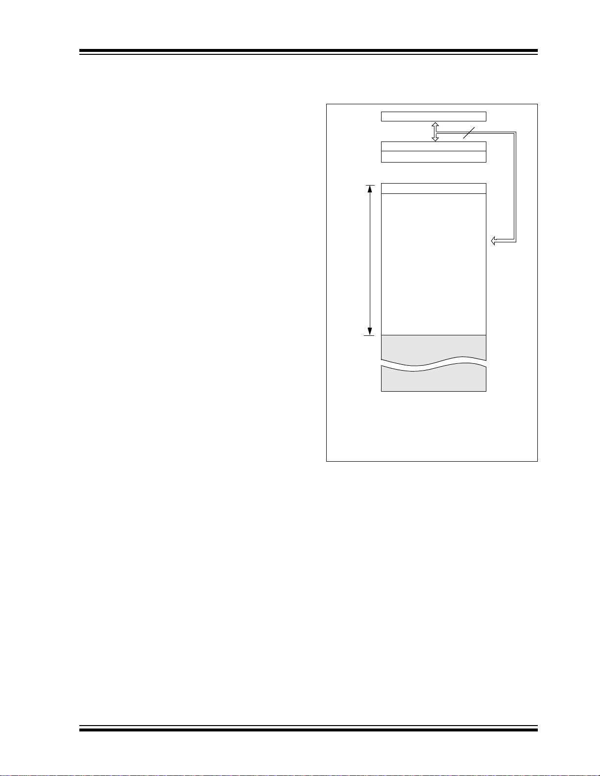
4.1 Program Memory Organization for
the PIC10F200/204
The PIC10F200/204 devices have a 9-bit Program
Counter (PC) capable of addressing a 512 x 12
program memory space.
Only the first 256 x 12 (0000h-00FFh) for the
PIC10F200/204 are physically implemented (see
Figure 4-1). Accessing a location above these
boundaries will cause a wraparound within the first
256 x 12 space (PIC10F200/204). The effective
Reset vector is at 0000h (see Figure 4-1). Location
00FFh (PIC10F200/204) contains the internal clock
oscillator calibration value. This value should never
be overwritten.
FIGURE 4-1: PROGRAM MEMORY MAP
AND STACK FOR THE
PIC10F200/204
PC<7:0>
CALL, RETLW
Stack Level 1
Stack Level 2
Reset Vector
On-chip Program
Memory
Space
User Memory
256 Word
9
(1)
0000h
00FFh
0100h
Note 1: Address 0000h becomes the
effective Reset vector. Location
00FFh contains the MOVLW XX
internal oscillator calibration value.
01FFh
© 2007 Microchip Technology Inc. DS41239D-page 15
PIC10F200/202/204/206
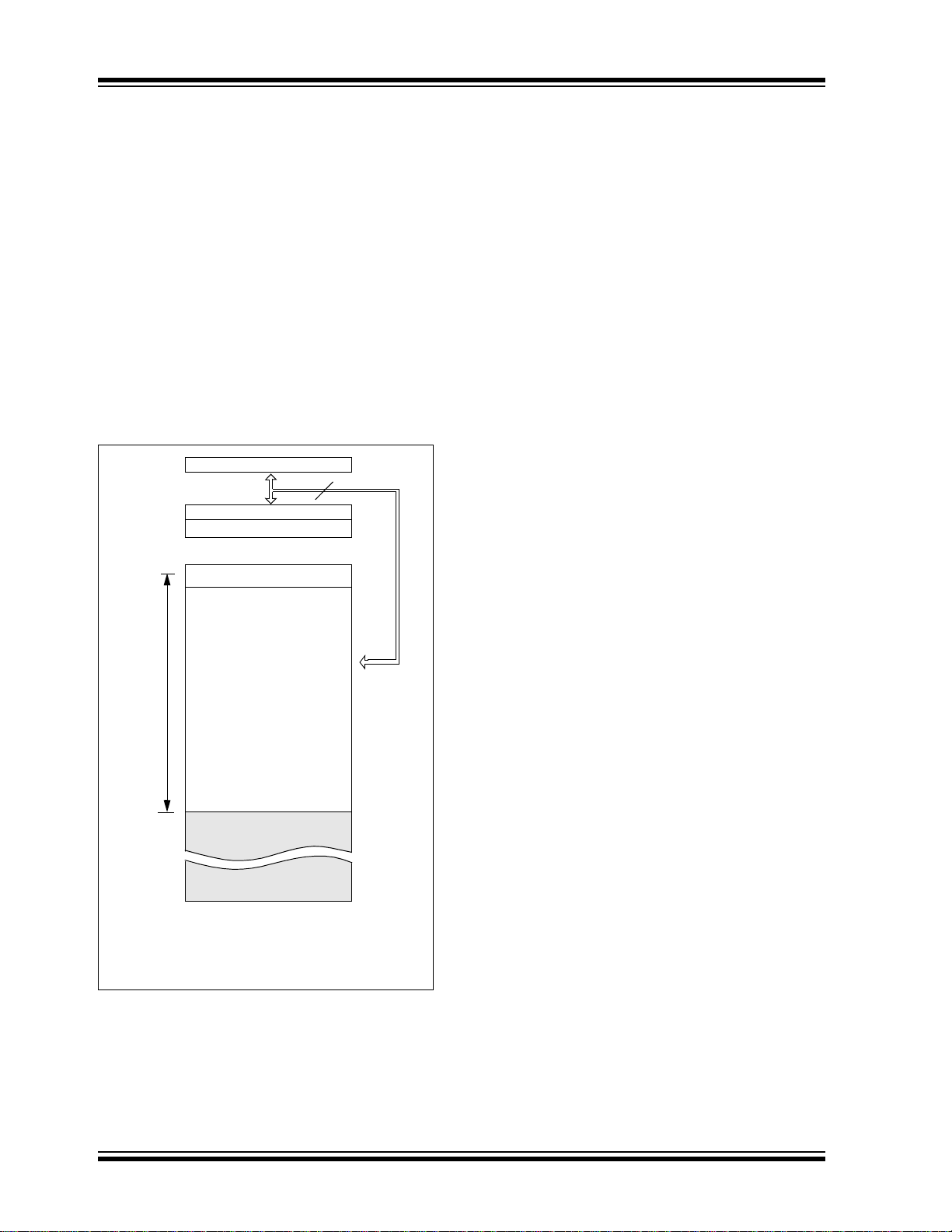
4.2 Program Memory Organization for
the PIC10F202/206
The PIC10F202/206 devices have a 10-bit Program
Counter (PC) capable of addressing a 1024 x 12
program memory space.
Only the first 512 x 12 (0000h-01FFh) for the
PIC10F202/206 are physically implemented (see
Figure 4-2). Accessing a location above these
boundaries will cause a wraparound within the first
512 x 12 space (PIC10F202/206). The effective
Reset vector is at 0000h (see Figure 4-2). Location
01FFh (PIC10F202/206) contains the internal clock
oscillator calibration value. This value should never
be overwritten.
FIGURE 4-2: PROGRAM MEMORY MAP
AND STACK FOR THE
PIC10F202/206
PC<8:0>
CALL, RETLW
Stack Level 1
Stack Level 2
Reset Vector
On-chip Program
Memory
10
(1)
0000h
4.3 Data Memory Organization
Data memory is composed of registers or bytes of
RAM. Therefore, data memory for a device is specified
by its register file. The register file is divided into two
functional groups: Special Function Registers (SFR)
and General Purpose Registers (GPR).
The Special Function Registers include the TMR0 register, the Program Counter (PCL), the STATUS register,
the I/O register (GPIO) and the File Select Register
(FSR). In addition, Special Function Registers are used
to control the I/O port configuration and prescaler
options.
The General Purpose registers are used for data and
control information under command of the instructions.
For the PIC10F200/204, the register file is composed of
7 Special Function registers and 16 General Purpose
registers (see Figure 4-3 and Figure 4-4).
For the PIC10F202/206, the register file is composed of
8 Special Function registers and 24 General Purpose
registers (see Figure 4-4).
4.3.1 GENERAL PURPOSE REGISTER
FILE
The General Purpose Register file is accessed, either
directly or indirectly, through the File Select Register
(FSR). See Section 4.9 “Indirect Data Addressing:
INDF and FSR Registers”.
Space
User Memory
512 Words
Note 1: Address 0000h becomes the
effective Reset vector. Location
01FFh contains the MOVLW XX
internal oscillator calibration value.
01FFh
0200h
02FFh
DS41239D-page 16 © 2007 Microchip Technology Inc.
PIC10F200/202/204/206
FIGURE 4-3: PIC10F200/204 REGISTER
FILE MAP
File Address
(1)
00h
01h
02h
03h
04h
05h
06h
07h
08h
0Fh
10h
1Fh
Note 1: Not a physical register. See Section 4.9
“Indirect Data Addressing: INDF and
FSR Registers”.
2: PIC10F204 only. Unimplemented on the
PIC10F200 and reads as 00h.
3: Unimplemented, read as 00h.
INDF
TMR0
PCL
STATUS
FSR
OSCCAL
GPIO
General
Purpose
(2)
CMCON0
Unimplemented
Registers
(3)
FIGURE 4-4: PIC10F202/206 REGISTER
FILE MAP
File Address
(1)
00h
01h
02h
03h
04h
05h
06h
07h
08h
1Fh
Note 1: Not a physical register. See Section 4.9
“Indirect Data Addressing: INDF and
FSR Registers”.
2: PIC10F206 only. Unimplemented on the
PIC10F202 and reads as 00h.
INDF
TMR0
PCL
STATUS
FSR
OSCCAL
GPIO
CMCON0
General
Purpose
Registers
(2)
© 2007 Microchip Technology Inc. DS41239D-page 17
PIC10F200/202/204/206
4.3.2 SPECIAL FUNCTION REGISTERS
The Special Function Registers (SFRs) are registers
used by the CPU and peripheral functions to control the
operation of the device (Table 4-1).
The Special Function Registers can be classified into
two sets. The Special Function Registers associated
with the “core” functions are described in this section.
Those related to the operation of the peripheral
features are described in the section for each
peripheral feature.
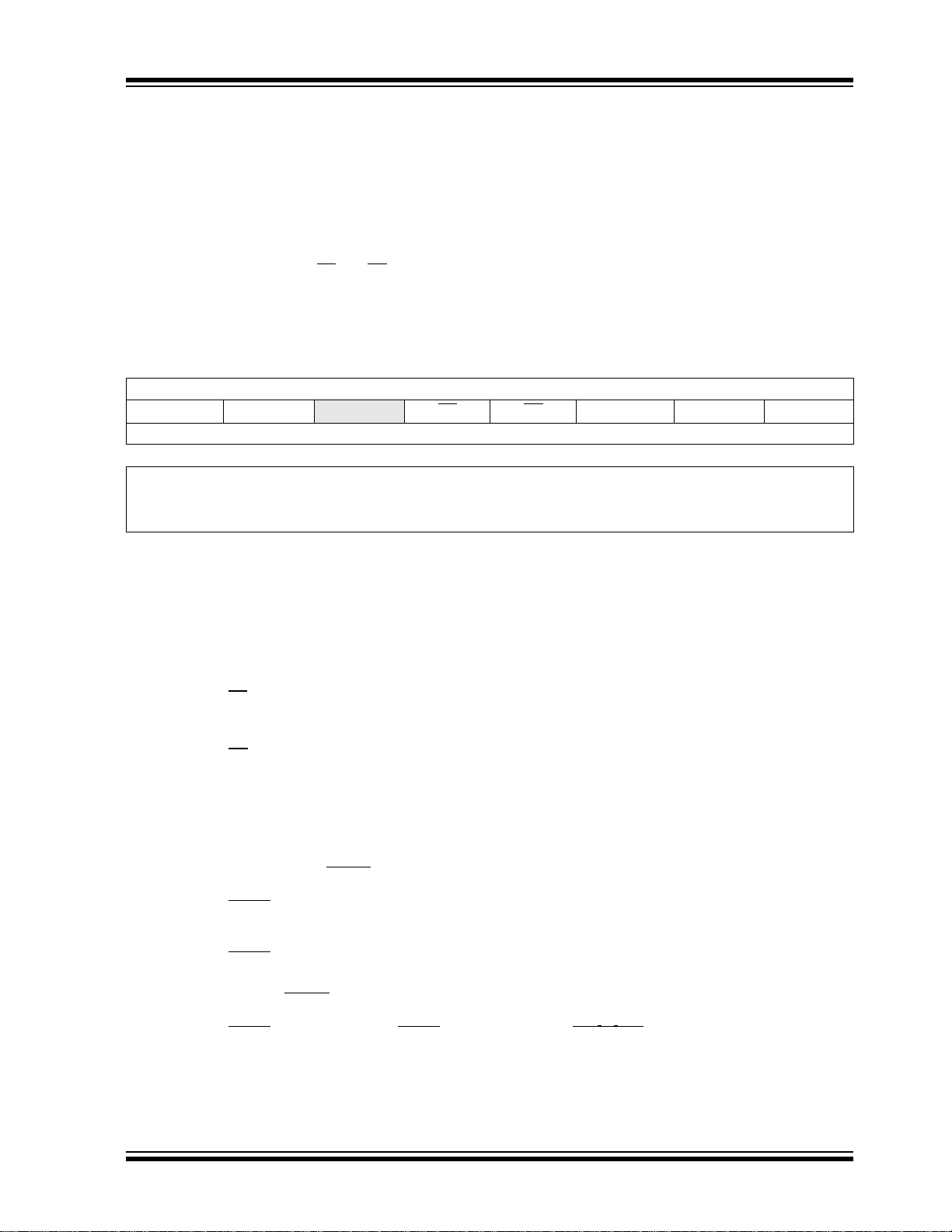
TABLE 4-1: SPECIAL FUNCTION REGISTER (SFR) SUMMARY (PIC10F200/202/204/206)
Address Name Bit 7 Bit 6 Bit 5 Bit 4 Bit 3 Bit 2 Bit 1 Bit 0
00h INDF Uses Contents of FSR to Address Data Memory (not a physical register) xxxx xxxx 23
01h TMR0 8-bit Real-Time Clock/Counter xxxx xxxx 29, 33
(1)
02h
03h STATUS GPWUF CWUF
04h FSR Indirect Data Memory Address Pointer 111x xxxx 23
05h OSCCAL CAL6 CAL5 CAL4 CAL3 CAL2 CAL1 CAL0 FOSC4 1111 1110 21
06h GPIO
07h
N/A TRISGPIO
N/A OPTION GPWU
Legend: – = unimplemented, read as ‘0’, x = unknown, u = unchanged, q = value depends on condition.
Note 1: The upper byte of the Program Counter is not directly accessible. See Section 4.7 “Program Counter” for an
PCL Low-order 8 bits of PC 1111 1111 22
(5)
—TOPD ZDCC00-1 1xxx
— — — — GP3 GP2 GP1 GP0 ---- xxxx 25
(4)
CMCON0 CMPOUT COUTEN POL CMPT0CS CMPON CNREF CPREF CWU 1111 1111 34
— — — — I/O Control Register ---- 1111 37
GPPU T0CS T0SE PSA PS2 PS1 PS0 1111 1111 20
explanation of how to access these bits.
2: Other (non Power-up) Resets include external Reset through MCLR
Reset.
3: See Table 9-1 for other Reset specific values.
4: PIC10F204/206 only.
5: PIC10F204/206 only. On all other devices, this bit is reserved and should not be used.
, Watchdog Timer and wake-up on pin change
Value on
Power-On
(2)
Reset
(3)
Page #
19
DS41239D-page 18 © 2007 Microchip Technology Inc.
PIC10F200/202/204/206
4.4 STATUS Register
This register contains the arithmetic status of the ALU,
the Reset status and the page preselect bit.
The STATUS register can be the destination for any
instruction, as with any other register. If the STATUS
register is the destination for an instruction that affects
the Z, DC or C bits, then the write to these three bits is
disabled. These bits are set or cleared according to the
device logic. Furthermore, the TO
writable. Therefore, the result of an instruction with the
STATUS register as destination may be different than
intended.
and PD bits are not
For example, CLRF STATUS, will clear the upper three
bits and set the Z bit. This leaves the STATUS register
as 000u u1uu (where u = unchanged).
Therefore, it is recommended that only BCF, BSF and
MOVWF instructions be used to alter the STATUS register. These instructions do not affect the Z, DC or C bits
from the STATUS register. For other instructions which
do affect Status bits, see Section 10.0 “Instruction
Set Summary”.
REGISTER 4-1: STATUS REGISTER
R/W-0 R/W-0 R/W-0 R-1 R-1 R/W-x R/W-x R/W-x
GPWUF CWUF
bit 7 bit 0
Legend:
R = Readable bit W = Writable bit U = Unimplemented bit, read as ‘0’
-n = Value at POR ‘1’ = Bit is set ‘0’ = Bit is cleared x = Bit is unknown
bit 7 GPWUF: GPIO Reset bit
1 = Reset due to wake-up from Sleep on pin change
0 = After power-up or other Reset
bit 6 CWUF: Comparator Wake-up on Change Flag bit
1 = Reset due to wake-up from Sleep on comparator change
0 = After power-up or other Reset conditions.
bit 5 Reserved: Do not use. Use of this bit may affect upward compatibility with future products.
bit 4 TO
1 = After power-up, CLRWDT instruction or SLEEP instruction
0 = A WDT time-out occurred
bit 3 PD: Power-Down bit
1 = After power-up or by the CLRWDT instruction
0 = By execution of the SLEEP instruction
bit 2 Z: Zero bit
1 = The result of an arithmetic or logic operation is zero
0 = The result of an arithmetic or logic operation is not zero
bit 1 DC: Digit Carry/Borrow
ADDWF
1 = A carry from the 4th low-order bit of the result occurred
0 = A carry from the 4th low-order bit of the result did not occur
SUBWF
1 = A borrow from the 4th low-order bit of the result did not occur
0 = A borrow from the 4th low-order bit of the result occurred
bit 0 C: Carry/Borrow bit (for ADDWF, SUBWF and RRF, RLF instructions)
ADDWF
1 = A carry occurred 1 = A borrow did not occur Load bit with LSb or MSb, respectively
0 = A carry did not occur 0 = A borrow occurred
(1)
: Time-out bit
:
:
: SUBWF: RRF or RLF:
—TOPD ZDCC
(1)
bit (for ADDWF and SUBWF instructions)
Note 1: This bit is used on the PIC10F204/206. For code compatibility do not use this bit on the PIC10F200/202.
© 2007 Microchip Technology Inc. DS41239D-page 19

PIC10F200/202/204/206
4.5 OPTION Register
The OPTION register is a 8-bit wide, write-only register,
which contains various control bits to configure the
Timer0/WDT prescaler and Timer0.
By executing the OPTION instruction, the contents of
the W register will be transferred to the OPTION register. A Reset sets the OPTION<7:0> bits.
REGISTER 4-2: OPTION REGISTER
W-1 W-1 W-1 W-1 W-1 W-1 W-1 W-1
GPWU
bit 7 bit 0
Legend:
R = Readable bit W = Writable bit U = Unimplemented bit, read as ‘0’
-n = Value at POR ‘1’ = Bit is set ‘0’ = Bit is cleared x = Bit is unknown
GPPU T0CS T0SE PSA PS2 PS1 PS0
Note: If TRIS bit is set to ‘0’, the wake-up on
change and pull-up functions are disabled
for that pin (i.e., note that TRIS overrides
Option control of GPPU
Note: If the T0CS bit is set to ‘1’, it will override
the TRIS function on the T0CKI pin.
and GPWU).
bit 7 GPWU
bit 6 GPPU
bit 5 T0CS: Timer0 Clock Source Select bit
bit 4 T0SE: Timer0 Source Edge Select bit
bit 3 PSA: Prescaler Assignment bit
bit 2-0 PS<2:0>: Prescaler Rate Select bits
: Enable Wake-up on Pin Change bit (GP0, GP1, GP3)
1 = Disabled
0 = Enabled
: Enable Weak Pull-ups bit (GP0, GP1, GP3)
1 = Disabled
0 = Enabled
1 = Transition on T0CKI pin (overrides TRIS on the T0CKI pin)
0 = Transition on internal instruction cycle clock, F
1 = Increment on high-to-low transition on the T0CKI pin
0 = Increment on low-to-high transition on the T0CKI pin
1 = Prescaler assigned to the WDT
0 = Prescaler assigned to Timer0
Bit Value Timer0 Rate WDT Rate
000
001
010
011
100
101
110
111
1 : 2
1 : 4
1 : 8
1 : 16
1 : 32
1 : 64
1 : 128
1 : 256
OSC/4
1 : 1
1 : 2
1 : 4
1 : 8
1 : 16
1 : 32
1 : 64
1 : 128
.
DS41239D-page 20 © 2007 Microchip Technology Inc.

PIC10F200/202/204/206
4.6 OSCCAL Register
The Oscillator Calibration (OSCCAL) register is used to
calibrate the internal precision 4 MHz oscillator. It
contains seven bits for calibration
Note: Erasing the device will also erase the pre-
programmed internal calibration value for
the internal oscillator. The calibration
value must be read prior to erasing the
part so it can be reprogrammed correctly
later.
After you move in the calibration constant, do not
change the value. See Section 9.2.2 “Internal 4 MHz
Oscillator”.
REGISTER 4-3: OSCCAL REGISTER
R/W-1 R/W-1 R/W-1 R/W-1 R/W-1 R/W-1 R/W-1 R/W-0
CAL6 CAL5 CAL4 CAL3 CAL2 CAL1 CAL0 FOSC4
bit 7 bit 0
Legend:
R = Readable bit W = Writable bit U = Unimplemented bit, read as ‘0’
-n = Value at POR ‘1’ = Bit is set ‘0’ = Bit is cleared x = Bit is unknown
.
bit 7-1 CAL<6:0>: Oscillator Calibration bits
0111111 = Maximum frequency
•
•
•
0000001
0000000 = Center frequency
1111111
•
•
•
1000000 =Minimum frequency
(1)
bit 0 FOSC4: INTOSC/4 Output Enable bit
1 = INTOSC/4 output onto GP2
0 = GP2/T0CKI/COUT applied to GP2
Note 1: Overrides GP2/T0CKI/COUT control registers when enabled.
© 2007 Microchip Technology Inc. DS41239D-page 21

PIC10F200/202/204/206
4.7 Program Counter
As a program instruction is executed, the Program
Counter (PC) will contain the address of the next
program instruction to be executed. The PC value is
increased by one every instruction cycle, unless an
instruction changes the PC.
For a GOTO instruction, bits 8:0 of the PC are provided
by the GOTO instruction word. The Program Counter
Low (PCL) is mapped to PC<7:0>.
For a CALL instruction, or any instruction where the
PCL is the destination, bits 7:0 of the PC again are provided by the instruction word. However, PC<8> does
not come from the instruction word, but is always
cleared (Figure 4-5).
Instructions where the PCL is the destination, or modify
PCL instructions, include MOVWF PC, ADDWF PC and
BSF PC,5.
Note: Because PC<8> is cleared in the CALL
instruction or any modify PCL instruction,
all subroutine calls or computed jumps are
limited to the first 256 locations of any
program memory page (512 words long).
FIGURE 4-5: LOADING OF PC
BRANCH INSTRUCTIONS
GOTO Instruction
87 0
PC
PCL
Instruction Word
4.7.1 EFFECTS OF RESET
The PC is set upon a Reset, which means that the PC
addresses the last location in program memory (i.e.,
the oscillator calibration instruction). After executing
MOVLW XX, the PC will roll over to location 0000h and
begin executing user code.
4.8 Stack
The PIC10F200/204 devices have a 2-deep, 8-bit wide
hardware PUSH/POP stack.
The PIC10F202/206 devices have a 2-deep, 9-bit wide
hardware PUSH/POP stack.
A CALL instruction will PUSH the current value of Stack 1
into Stack 2 and then PUSH the current PC value,
incremented by one, into Stack Level 1. If more than two
sequential CALLs are executed, only the most recent two
return addresses are stored.
A RETLW instruction will POP the contents of Stack
Level 1 into the PC and then copy Stack Level 2
contents into level 1. If more than two sequential
RETLWs are executed, the stack will be filled with the
address previously stored in Stack Level 2.
Note 1: The W register will be loaded with the lit-
eral value specified in the instruction. This
is particularly useful for the implementation of the data look-up tables within the
program memory.
2: There are no Status bits to indicate stack
overflows or stack underflow conditions.
3: There are no instruction mnemonics
called PUSH or POP. These are actions
that occur from the execution of the CALL
and RETLW instructions.
CALL or Modify PCL Instruction
87 0
PC
Reset to ‘0’
DS41239D-page 22 © 2007 Microchip Technology Inc.
PCL
Instruction Word
PIC10F200/202/204/206
4.9 Indirect Data Addressing: INDF
and FSR Registers
The INDF register is not a physical register. Addressing
INDF actually addresses the register whose address is
contained in the FSR register (FSR is a pointer). This is
indirect addressing.
4.10 Indirect Addressing
• Register file 09 contains the value 10h
• Register file 0A contains the value 0Ah
• Load the value 09 into the FSR register
• A read of the INDF register will return the value
of 10h
• Increment the value of the FSR register by one
(FSR = 0A)
• A read of the INDR register now will return the
value of 0Ah.
Reading INDF itself indirectly (FSR = 0) will produce
00h. Writing to the INDF register indirectly results in a
no operation (although Status bits may be affected).
A simple program to clear RAM locations 10h-1Fh
using indirect addressing is shown in Example 4-1.
EXAMPLE 4-1: HOW TO CLEAR RAM
USING INDIRECT
ADDRESSING
MOVLW 0x10 ;initialize pointer
MOVWF FSR ;to RAM
NEXT CLRF INDF ;clear INDF
;register
INCF FSR,F ;inc pointer
BTFSC FSR,4 ;all done?
GOTO NEXT ;NO, clear next
CONTINUE
: ;YES, continue
:
The FSR is a 5-bit wide register. It is used in conjunction with the INDF register to indirectly address the data
memory area.
The FSR<4:0> bits are used to select data memory
addresses 00h to 1Fh.
Note: PIC10F200/202/204/206 – Do not use
banking. FSR <7:5> are unimplemented
and read as ‘1’s.
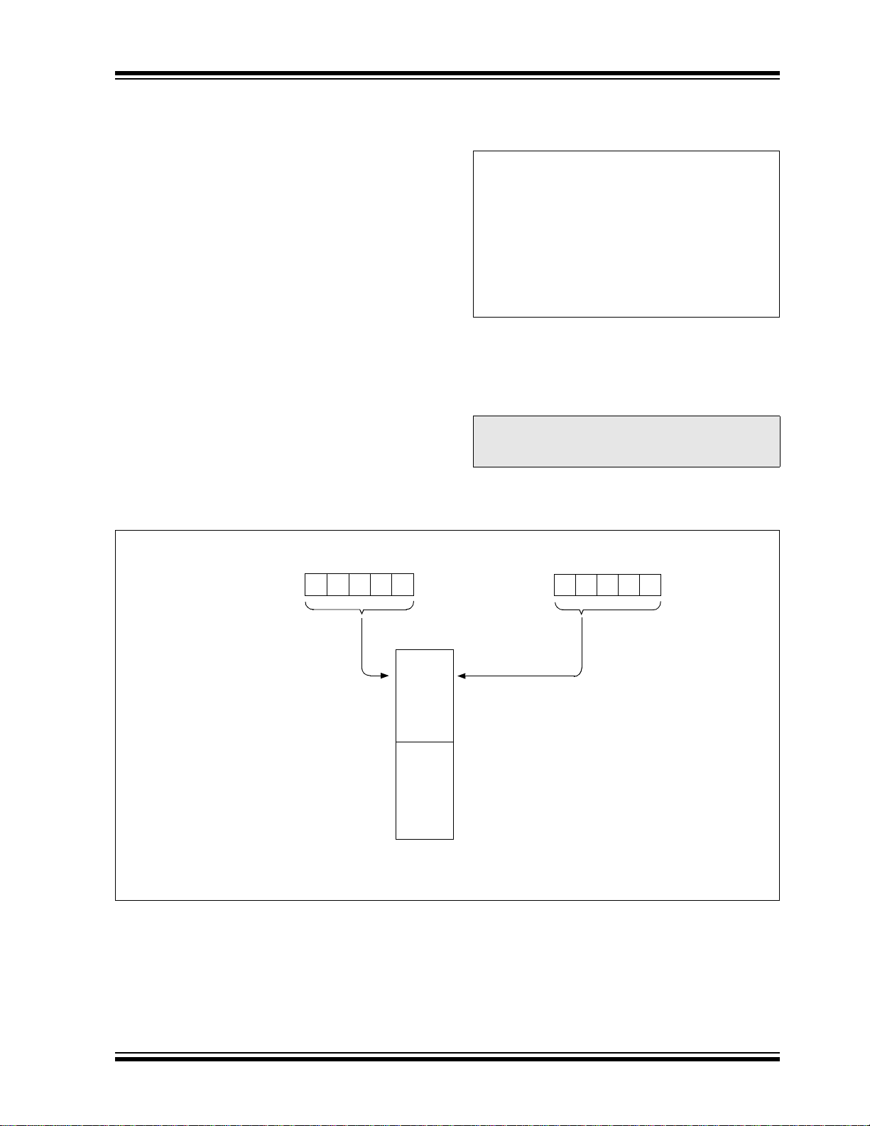
FIGURE 4-6: DIRECT/INDIRECT ADDRESSING (PIC10F200/202/204/206)
Direct Addressing
(opcode) 04
Location Select
00h
Data
Memory
Note 1: For register map detail, see Section 4.3 “Data Memory Organization”.
0Fh
(1)
10h
1Fh
Bank 0
Indirect Addressing
(FSR)
4
Location Select
0
© 2007 Microchip Technology Inc. DS41239D-page 23

PIC10F200/202/204/206
NOTES:
DS41239D-page 24 © 2007 Microchip Technology Inc.
PIC10F200/202/204/206
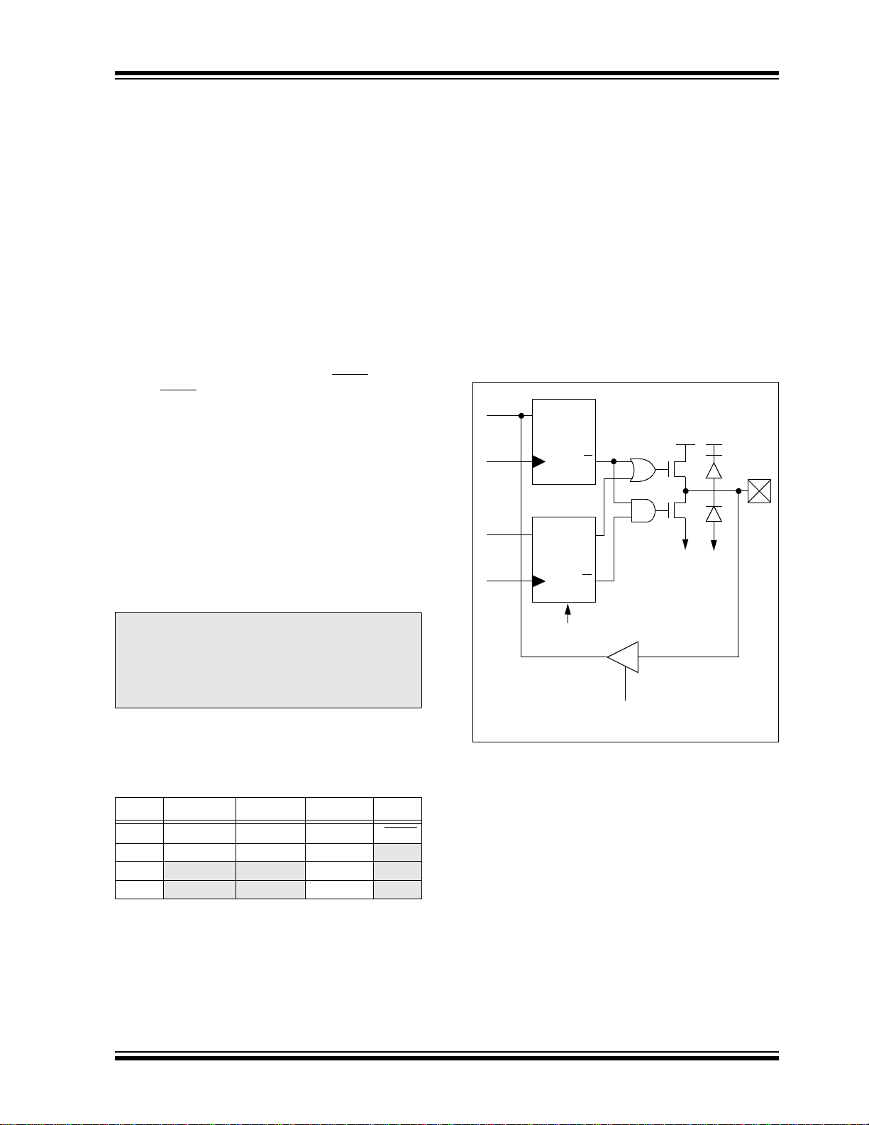
5.0 I/O PORT
As with any other register, the I/O register(s) can be
written and read under program control. However, read
instructions (e.g., MOVF GPIO, W) always read the I/O
pins independent of the pin’s Input/Output modes. On
Reset, all I/O ports are defined as input (inputs are at
high-impedance) since the I/O control registers are all
set.
5.1 GPIO
GPIO is an 8-bit I/O register. Only the low-order 4 bits
are used (GP<3:0>). Bits 7 through 4 are unimplemented and read as ‘0’s. Please note that GP3 is an
input-only pin. Pins GP0, GP1 and GP3 can be configured with weak pull-ups and also for wake-up on
change. The wake-up on change and weak pull-up
functions are not pin selectable. If GP3/MCLR
ured as MCLR
, weak pull-up is always on and wake-up
on change for this pin is not enabled.
5.2 TRIS Registers
The Output Driver Control register is loaded with the
contents of the W register by executing the TRIS f
instruction. A ‘1’ from a TRIS register bit puts the corresponding output driver in a High-Impedance mode. A
‘0’ puts the contents of the output data latch on the
selected pins, enabling the output buffer. The exceptions are GP3, which is input-only and the GP2/T0CKI/
COUT/FOSC4 pin, which may be controlled by various
registers. See Table 5-1.
is config-
5.3 I/O Interfacing
The equivalent circuit for an I/O port pin is shown in
Figure 5-1. All port pins, except GP3 which is inputonly, may be used for both input and output operations.
For input operations, these ports are non-latching. Any
input must be present until read by an input instruction
(e.g., MOVF GPIO, W). The outputs are latched and
remain unchanged until the output latch is rewritten. To
use a port pin as output, the corresponding direction
control bit in TRIS must be cleared (= 0). For use as an
input, the corresponding TRIS bit must be set. Any I/O
pin (except GP3) can be programmed individually as
input or output.
FIGURE 5-1: PIC10F200/202/204/206
EQUIVALENT CIRCUIT
FOR A SINGLE I/O PIN
Data
Bus
WR
Port
W
Reg
TRIS ‘f’
D
D
Data
Latch
CK
TRIS
Latch
CK
Q
VDD
VDD
Q
Q
Q
P
N
SS
VSS
V
I/O
pin
Note: A read of the ports reads the pins, not the
output data latches. That is, if an output
driver on a pin is enabled and driven high,
but the external system is holding it low, a
read of the port will indicate that the pin is
low.
The TRIS registers are “write-only” and are set (output
drivers disabled) upon Reset.
TABLE 5-1: ORDER OF PRECEDENCE
FOR PIN FUNCTIONS
Priority GP0 GP1 GP2 GP3
1 CIN+ CIN- FOSC4 I/MCLR
2 TRIS GPIO TRIS GPIO COUT —
3
4
— —T0CKI—
— —TRIS GPIO—
Reset
Note 1: See Table 3-2 for buffer type.
(1)
RD Port
© 2007 Microchip Technology Inc. DS41239D-page 25

PIC10F200/202/204/206
TABLE 5-2: SUMMARY OF PORT REGISTERS
Address Name Bit 7 Bit 6 Bit 5 Bit 4 Bit 3 Bit 2 Bit 1 Bit 0
N/A TRISGPIO
N/A OPTION GPWU
03h STATUS GPWUF CWUF
06h GPIO — — — — GP3 GP2 GP1 GP0 ---- xxxx ---- uuuu
Legend: Shaded cells are not used by PORT registers, read as ‘0’, – = unimplemented, read as ‘0’, x = unknown, u =
unchanged,
q = depends on condition.
Note 1: If Reset was due to wake-up on pin change, then bit 7 = 1. All other Resets will cause bit 7 = 0.
2: If Reset was due to wake-up on comparator change, then bit 6 = 1. All other Resets will cause bit 6 = 0.
— — — — I/O Control Register
GPPU T0CS T0SE PSA PS2 PS1 PS0 1111 1111
— TO PD Z DC C 00-1 1xxx
Value on
Power-On
Reset
---- 1111
Value on
All Other Resets
---- 1111
1111 1111
qq-q quuu
(1), (2)
5.4 I/O Programming Considerations
5.4.1 BIDIRECTIONAL I/O PORTS
Some instructions operate internally as read followed
by write operations. The BCF and BSF instructions, for
example, read the entire port into the CPU, execute the
bit operation and rewrite the result. Caution must be
used when these instructions are applied to a port
where one or more pins are used as input/outputs. For
example, a BSF operation on bit 2 of GPIO will cause
all eight bits of GPIO to be read into the CPU, bit 2 to
be set and the GPIO value to be written to the output
latches. If another bit of GPIO is used as a bidirectional
I/O pin (say bit 0), and it is defined as an input at this
time, the input signal present on the pin itself would be
read into the CPU and rewritten to the data latch of this
particular pin, overwriting the previous content. As long
as the pin stays in the Input mode, no problem occurs.
However, if bit 0 is switched into Output mode later on,
the content of the data latch may now be unknown.
Example 5-1 shows the effect of two sequential
Read-Modify-Write instructions (e.g., BCF, BSF, etc.)
on an I/O port.
A pin actively outputting a high or a low should not be
driven from external devices at the same time in order
to change the level on this pin (“wired OR”, “wired
AND”). The resulting high output currents may damage
the chip.
EXAMPLE 5-1: READ-MODIFY-WRITE
INSTRUCTIONS ON AN
I/O PORT
;Initial GPIO Settings
;GPIO<3:2> Inputs
;GPIO<1:0> Outputs
;
; GPIO latch GPIO pins
; ---------- ----------
BCF GPIO, 1 ;---- pp01 ---- pp11
BCF GPIO, 0 ;---- pp10 ---- pp11
MOVLW 007h;
TRIS GPIO ;---- pp10 ---- pp11
;
Note 1: The user may have expected the pin val-
ues to be
GP1 to be latched as the pin value (High).
---- pp00. The 2nd BCF caused
5.4.2 SUCCESSIVE OPERATIONS ON
I/O PORTS
The actual write to an I/O port happens at the end of an
instruction cycle, whereas for reading, the data must be
valid at the beginning of the instruction cycle (Figure 5-2).
Therefore, care must be exercised if a write followed by
a read operation is carried out on the same I/O port. The
sequence of instructions should allow the pin voltage to
stabilize (load dependent) before the next instruction
causes that file to be read into the CPU. Otherwise, the
previous state of that pin may be read into the CPU rather
than the new state. When in doubt, it is better to separate
these instructions with a NOP or another instruction not
accessing this I/O port.
DS41239D-page 26 © 2007 Microchip Technology Inc.
PIC10F200/202/204/206
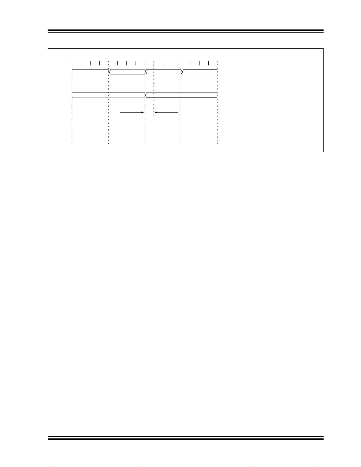
FIGURE 5-2: SUCCESSIVE I/O OPERATION (PIC10F200/202/204/206)
Q1 Q2 Q3 Q4 Q1 Q2 Q3 Q4 Q1 Q2 Q3 Q4 Q1 Q2 Q3 Q4
Instruction
Fetched
GP<2:0>
Instruction
Executed
PC PC + 1 PC + 2
MOVWF GPIO NOP
Port pin
written here
MOVWF GPIO
(Write to GPIO)
Port pin
sampled here
(Read GPIO)
PC + 3
NOPMOVF GPIO, W
NOPMOVF GPIO,W
This example shows a write to GPIO followed
by a read from GPIO.
Data setup time = (0.25 T
where: T
CY = instruction cycle
PD = propagation delay
T
Therefore, at higher clock frequencies, a
write followed by a read may be problematic.
CY – TPD)
© 2007 Microchip Technology Inc. DS41239D-page 27

PIC10F200/202/204/206
NOTES:
DS41239D-page 28 © 2007 Microchip Technology Inc.

PIC10F200/202/204/206
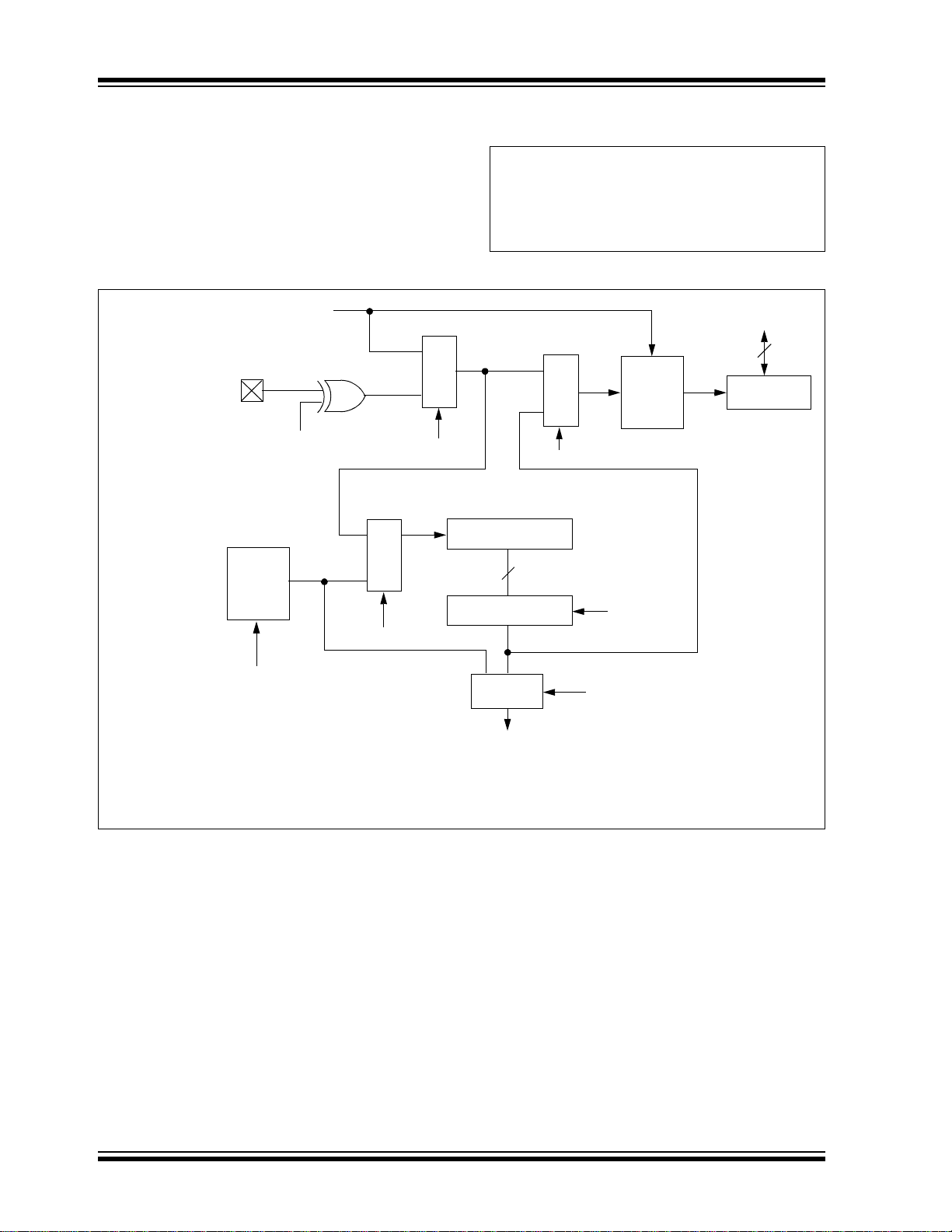
6.0 TIMER0 MODULE AND TMR0
REGISTER (PIC10F200/202)
The Timer0 module has the following features:
• 8-bit timer/counter register, TMR0
• Readable and writable
• 8-bit software programmable prescaler
• Internal or external clock select:
- Edge select for external clock
Figure 6-1 is a simplified block diagram of the Timer0
module.
Timer mode is selected by clearing the T0CS bit
(OPTION<5>). In Timer mode, the Timer0 module will
increment every instruction cycle (without prescaler). If
TMR0 register is written, the increment is inhibited for
the following two cycles (Figure 6-2 and Figure 6-3).
The user can work around this by writing an adjusted
value to the TMR0 register.
FIGURE 6-1: TIMER0 BLOCK DIAGRAM
GP2/T0CKI
Pin
T0SE
FOSC/4
(1)
0
1
T0CS
Programmable
PS2, PS1, PS0
(1)
Prescaler
Counter mode is selected by setting the T0CS bit
(OPTION<5>). In this mode, Timer0 will increment
either on every rising or falling edge of pin T0CKI. The
T0SE bit (OPTION<4>) determines the source edge.
Clearing the T0SE bit selects the rising edge. Restrictions on the external clock input are discussed in detail
in Section 6.1 “Using Timer0 with an External Clock
(PIC10F200/202)”.
The prescaler may be used by either the Timer0
module or the Watchdog Timer, but not both. The
prescaler assignment is controlled in software by the
control bit, PSA (OPTION<3>). Clearing the PSA bit
will assign the prescaler to Timer0. The prescaler is not
readable or writable. When the prescaler is assigned to
the Timer0 module, prescale values of 1:2, 1:4, 1:256
are selectable. Section 6.2 “Prescaler” details the
operation of the prescaler.
A summary of registers associated with the Timer0
module is found in Table 6-1.
Data Bus
PS
OUT
1
(2)
3
0
PSA
(1)
(1)
Sync with
Internal
Clocks
(2 TCY delay)
TMR0 Reg
PSOUT
Sync
8
Note 1: Bits T0CS, T0SE, PSA, PS2, PS1 and PS0 are located in the OPTION register.
2: The prescaler is shared with the Watchdog Timer (Figure 6-5).
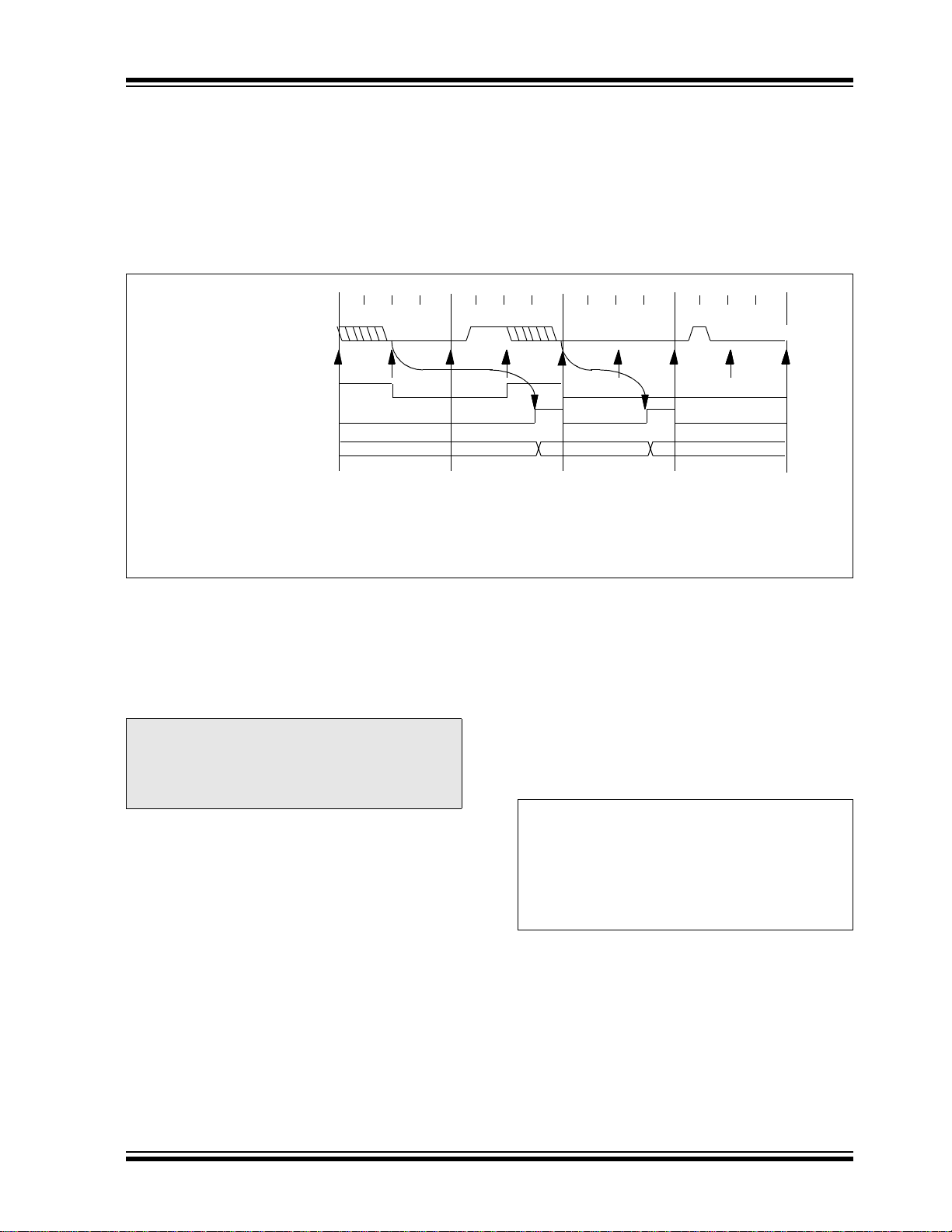
FIGURE 6-2: TIMER0 TIMING: INTERNAL CLOCK/NO PRESCALE
PC
(Program
Counter)
Instruction
Fetch
Timer0
Instruction
Executed
Q1 Q2 Q3 Q4
PC – 1
T0
Q1 Q2 Q3 Q4 Q1 Q2 Q3 Q4 Q1 Q2 Q3 Q4 Q1 Q2 Q3 Q4 Q1 Q2 Q3 Q4 Q1 Q2 Q3 Q4 Q1 Q2 Q3 Q4
PC PC + 1 PC + 2 PC + 3 PC + 4 PC + 6
MOVWF TMR0 MOVF TMR0,W MOVF TMR0,W MOVF TMR0,W MOVF TMR0,W MOVF TMR0,W
T0 + 1 T0 + 2 NT0
Write TMR0
executed
Read TMR0
reads NT0
Read TMR0
reads NT0
Read TMR0
reads NT0
PC + 5
NT0 + 1
Read TMR0
reads NT0 + 1
NT0 + 2
Read TMR0
reads NT0 + 2
© 2007 Microchip Technology Inc. DS41239D-page 29

PIC10F200/202/204/206
FIGURE 6-3: TIMER0 TIMING: INTERNAL CLOCK/PRESCALE 1:2
PC
(Program
Counter)
Instruction
Fetch
Timer0
Instruction
Executed
Q1 Q2 Q3 Q4
PC – 1
T0
Q1 Q2 Q3 Q4 Q1 Q2 Q3 Q4 Q1 Q2 Q3 Q4 Q1 Q2 Q3 Q4 Q1 Q2 Q3 Q4 Q1 Q2 Q3 Q4 Q1 Q2 Q3 Q4
PC PC + 1 PC + 2 PC + 3 PC + 4 PC + 6
MOVWF TMR0 MOVF TMR0,W MOVF TMR0,W MOVF TMR0,W MOVF TMR0,W MOVF TMR0,W
T0 + 1 NT0
Write TMR0
executed
Read TMR0
reads NT0
Read TMR0
reads NT0
Read TMR0
reads NT0
PC + 5
Read TMR0
reads NT0 + 1
TABLE 6-1: REGISTERS ASSOCIATED WITH TIMER0
Value on
Address Name Bit 7 Bit 6 Bit 5 Bit 4 Bit 3 Bit 2 Bit 1 Bit 0
01h TMR0 Timer0 – 8-bit Real-Time Clock/Counter xxxx xxxx
N/A OPTION GPWU GPPU T0CS T0SE PSA PS2 PS1 PS0 1111 1111
N/A TRISGPIO
(1)
— —
— —
I/O Control Register ---- 1111
Legend: Shaded cells not used by Timer0. – = unimplemented, x = unknown, u = unchanged.
Note 1: The TRIS of the T0CKI pin is overridden when T0CS = 1.
6.1 Using Timer0 with an External
Clock (PIC10F200/202)
When an external clock input is used for Timer0, it must
meet certain requirements. The external clock requirement is due to internal phase clock (TOSC) synchroniza-
tion. Also, there is a delay in the actual incrementing of
Timer0 after synchronization.
6.1.1 EXTERNAL CLOCK
SYNCHRONIZATION
When no prescaler is used, the external clock input is
the same as the prescaler output. The synchronization
of T0CKI with the internal phase clocks is accomplished by sampling the prescaler output on the Q2 and
Q4 cycles of the internal phase clocks (Figure 6-4).
Therefore, it is necessary for T0CKI to be high for at
least 2 T
for at least 2 T
OSC (and a small RC delay of 2 Tt0H) and low
OSC (and a small RC delay of 2 Tt0H).
Refer to the electrical specification of the desired
device.
When a prescaler is used, the external clock input is
divided by the asynchronous ripple counter-type
prescaler, so that the prescaler output is symmetrical.
For the external clock to meet the sampling requirement, the ripple counter must be taken into account.
Therefore, it is necessary for T0CKI to have a period of
at least 4 T
OSC (and a small RC delay of 4 Tt0H) divided
by the prescaler value. The only requirement on T0CKI
high and low time is that they do not violate the
minimum pulse width requirement of Tt0H. Refer to
parameters 40, 41 and 42 in the electrical specification
of the desired device.
Power-On
Reset
NT0 + 1
Read TMR0
reads NT0 + 2
Value on
All Other
Resets
uuuu uuuu
1111 1111
---- 1111
DS41239D-page 30 © 2007 Microchip Technology Inc.

PIC10F200/202/204/206
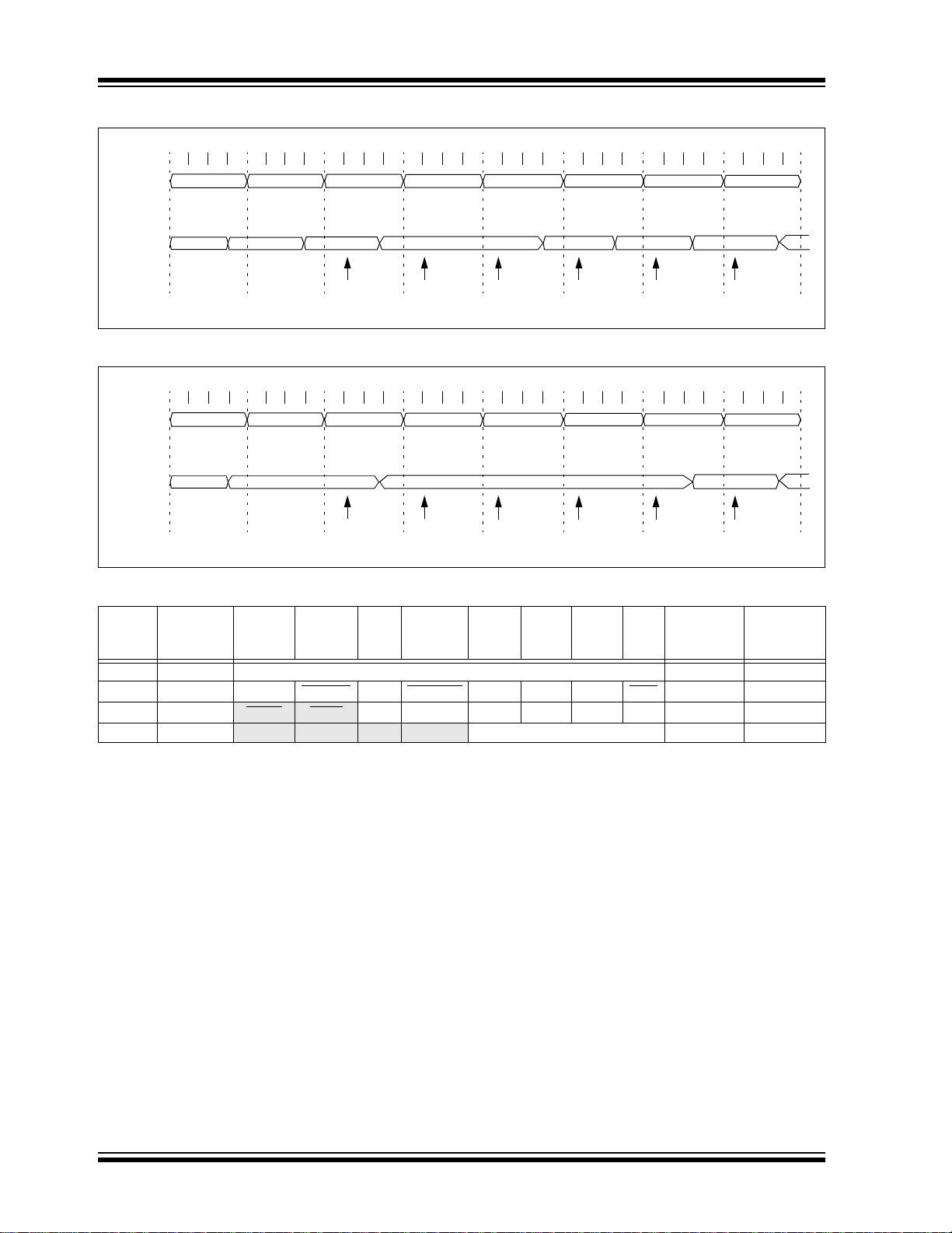
6.1.2 TIMER0 INCREMENT DELAY
Since the prescaler output is synchronized with the
internal clocks, there is a small delay from the time the
external clock edge occurs to the time the Timer0
module is actually incremented. Figure 6-4 shows the
delay from the external clock edge to the timer
incrementing.
FIGURE 6-4: TIMER0 TIMING WITH EXTERNAL CLOCK
Q1 Q2 Q3 Q4 Q1 Q2 Q3 Q4 Q1 Q2 Q3 Q4 Q1 Q2 Q3 Q4
External Clock Input or
Prescaler Output
External Clock/Prescaler
Output After Sampling
Increment Timer0 (Q4)
(2)
(1)
(3)
Small pulse
misses sampling
Timer0
Note 1: Delay from clock input change to Timer0 increment is 3 T
in measuring the interval between two edges on Timer0 input = ±4 T
2: External clock if no prescaler selected; prescaler output otherwise.
3: The arrows indicate the points in time where sampling occurs.
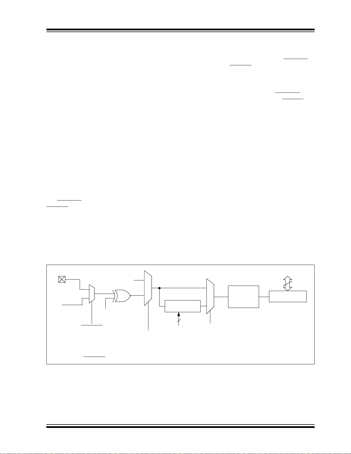
6.2 Prescaler
An 8-bit counter is available as a prescaler for the
Timer0 module or as a postscaler for the Watchdog
Timer (WDT), respectively (see Section 9.6 “Watch-
dog Timer (WDT)”). For simplicity, this counter is
being referred to as “prescaler” throughout this data
sheet.
Note: The prescaler may be used by either the
Timer0 module or the WDT, but not both.
Thus, a prescaler assignment for the
Timer0 module means that there is no
prescaler for the WDT and vice versa.
The PSA and PS<2:0> bits (OPTION<3:0>) determine
prescaler assignment and prescale ratio.
When assigned to the Timer0 module, all instructions
writing to the TMR0 register (e.g., CLRF 1, MOVWF 1,
BSF 1,x, etc.) will clear the prescaler. When assigned
to WDT, a CLRWDT instruction will clear the prescaler
along with the WDT. The prescaler is neither readable
nor writable. On a Reset, the prescaler contains all ‘0’s.
T0 T0 + 1 T0 + 2
OSC to 7 TOSC (Duration of Q = TOSC). Therefore, the error
OSC max.
6.2.1 SWITCHING PRESCALER
ASSIGNMENT
The prescaler assignment is fully under software
control (i.e., it can be changed “on-the-fly” during program execution). To avoid an unintended device Reset,
the following instruction sequence (Example 6-1) must
be executed when changing the prescaler assignment
from Timer0 to the WDT.
EXAMPLE 6-1: CHANGING PRESCALER
(TIMER0 → WDT)
CLRWDT ;Clear WDT
CLRF TMR0 ;Clear TMR0 & Prescaler
MOVLW ‘00xx1111’b ;These 3 lines (5, 6, 7)
OPTION ;are required only if
;desired
CLRWDT ;PS<2:0> are 000 or 001
MOVLW ‘00xx1xxx’b ;Set Postscaler to
OPTION ;desired WDT rate
© 2007 Microchip Technology Inc. DS41239D-page 31
PIC10F200/202/204/206
To change the prescaler from the WDT to the Timer0
EXAMPLE 6-2: CHANGING PRESCALER
module, use the sequence shown in Example 6-2. This
sequence must be used even if the WDT is disabled. A
CLRWDT instruction should be executed before
switching the prescaler.
CLRWDT ;Clear WDT and
MOVLW ‘xxxx0xxx’ ;Select TMR0, new
OPTION
FIGURE 6-5: BLOCK DIAGRAM OF THE TIMER0/WDT PRESCALER
TCY (= FOSC/4)
PSA
0
M
U
X
1
(1)
T0CS
M
U
X
(1)
8-bit Prescaler
8-to-1 MUX
1
M
U
X
0
(1)
PSA
8
PS<2:0>
GP2/T0CKI
Pin
Watchdog
Timer
(2)
T0SE
(1)
0
1
(WDT→TIMER0)
;prescaler
;prescale value and
;clock source
Data Bus
Sync
2
Cycles
(1)
TMR0 Reg
8
WDT Enable bit
Note 1: T0CS, T0SE, PSA, PS<2:0> are bits in the OPTION register.
2: T0CKI is shared with pin GP2 on the PIC10F200/202/204/206.
0
Time-out
MUX
WDT
1
(1)
PSA
DS41239D-page 32 © 2007 Microchip Technology Inc.
PIC10F200/202/204/206
7.0 TIMER0 MODULE AND TMR0
REGISTER (PIC10F204/206)
The Timer0 module has the following features:
• 8-bit timer/counter register, TMR0
• Readable and writable
• 8-bit software programmable prescaler
• Internal or external clock select:
- Edge select for external clock
- External clock from either the T0CKI pin or
from the output of the comparator
Figure 7-1 is a simplified block diagram of the Timer0
module.
Timer mode is selected by clearing the T0CS bit
(OPTION<5>). In Timer mode, the Timer0 module will
increment every instruction cycle (without prescaler). If
TMR0 register is written, the increment is inhibited for
the following two cycles (Figure 7-2 and Figure 7-3).
The user can work around this by writing an adjusted
value to the TMR0 register.
There are two types of Counter mode. The first Counter
mode uses the T0CKI pin to increment Timer0. It is
selected by setting the T0CS bit (OPTION<5>), setting
the CMPT0CS
COUTEN
increment either on every rising or falling edge of pin
T0CKI. The T0SE bit (OPTION<4>) determines the
source edge. Clearing the T0SE bit selects the rising
edge. Restrictions on the external clock input are
discussed in detail in Section 7.1 “Using Timer0 with
an External Clock (PIC10F204/206)”.
bit (CMCON0<4>) and setting the
bit (CMCON0<6>). In this mode, Timer0 will
The second Counter mode uses the output of the comparator to increment Timer0. It can be entered in two
different ways. The first way is selected by setting the
T0CS bit (OPTION<5>) and clearing the CMPT0CS
(CMCON<4>); (COUTEN
[CMCON<6>]) does not
bit
affect this mode of operation. This enables an internal
connection between the comparator and the Timer0.
The second way is selected by setting the T0CS bit
(OPTION<5>), setting the CMPT0CS
(CMCON0<4>) and clearing the COUTEN
bit
bit
(CMCON0<6>). This allows the output of the comparator onto the T0CKI pin, while keeping the T0CKI input
active. Therefore, any comparator change on the
COUT pin is fed back into the T0CKI input. The T0SE
bit (OPTION<4>) determines the source edge. Clearing the T0SE bit selects the rising edge. Restrictions on
the external clock input as discussed in Section 7.1
“Using Timer0 with an External Clock (PIC10F204/
206)”
The prescaler may be used by either the Timer0
module or the Watchdog Timer, but not both. The
prescaler assignment is controlled in software by the
control bit, PSA (OPTION<3>). Clearing the PSA bit
will assign the prescaler to Timer0. The prescaler is not
readable or writable. When the prescaler is assigned to
the Timer0 module, prescale values of 1:2, 1:4,...,
1:256 are selectable. Section 7.2 “Prescaler” details
the operation of the prescaler.
A summary of registers associated with the Timer0
module is found in Table 7-1.
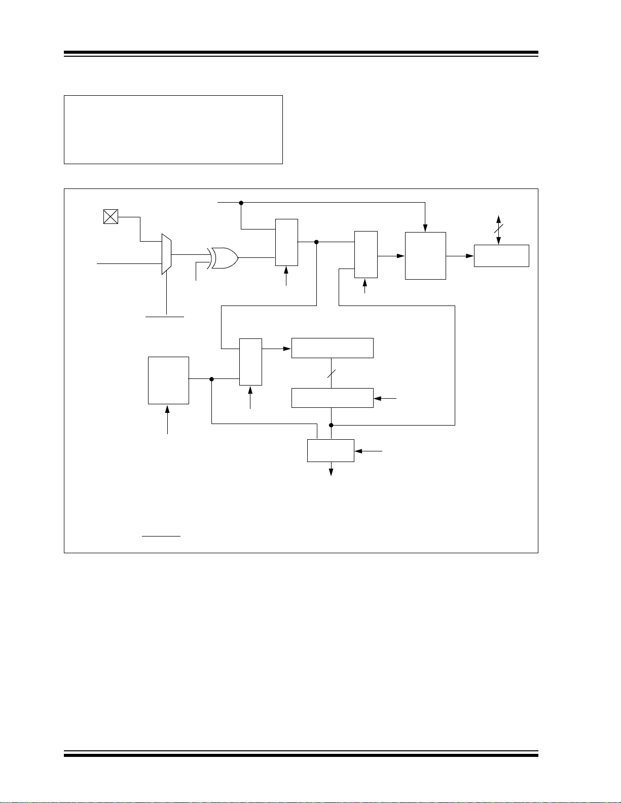
FIGURE 7-1: TIMER0 BLOCK DIAGRAM (PIC10F204/206)
T0CKI
Pin
FOSC/4
Internal
Comparator
Output
Note 1: Bits T0CS, T0SE, PSA, PS2, PS1 and PS0 are located in the OPTION register.
2: The prescaler is shared with the Watchdog Timer (Figure 7-5).
3: Bit CMPT0CS
1
0
CMPT0CS
(1)
T0SE
(3)
is located in the CMCON0 register, CMCON0<4>.
0
T0CS
1
(1)
Programmable
Prescaler
3
PS2, PS1, PS0
OUT
PS
1
(2)
0
PSA
(1)
(1)
Sync with
Internal
Clocks
(2 TCY delay)
Data Bus
8
TMR0 Reg
PSOUT
Sync
© 2007 Microchip Technology Inc. DS41239D-page 33
PIC10F200/202/204/206
FIGURE 7-2: TIMER0 TIMING: INTERNAL CLOCK/NO PRESCALE
PC
(Program
Counter)
Instruction
Fetch
Timer0
Instruction
Executed
Q1 Q2 Q3 Q4
PC – 1
T0
Q1 Q2 Q3 Q4 Q1 Q2 Q3 Q4 Q1 Q2 Q3 Q4 Q1 Q2 Q3 Q4 Q1 Q2 Q3 Q4 Q1 Q2 Q3 Q4 Q1 Q2 Q3 Q4
PC PC + 1 PC + 2 PC + 3 PC + 4 PC + 6
MOVWF TMR0 MOVF TMR0,W MOVF TMR0,W MOVF TMR0,W MOVF TMR0,W MOVF TMR0,W
T0 + 1 T0 + 2 NT0
Write TMR0
executed
Read TMR0
reads NT0
Read TMR0
reads NT0
Read TMR0
reads NT0
PC+5
NT0 + 1
Read TMR0
reads NT0 + 1
NT0 + 2
Read TMR0
reads NT0 + 2
FIGURE 7-3: TIMER0 TIMING: INTERNAL CLOCK/PRESCALE 1:2
PC
(Program
Counter)
Instruction
Fetch
Timer0
Instruction
Executed
Q1 Q2 Q3 Q4
PC – 1
T0
Q1 Q2 Q3 Q4 Q1 Q2 Q3 Q4 Q1 Q2 Q3 Q4 Q1 Q2 Q3 Q4 Q1 Q2 Q3 Q4 Q1 Q2 Q3 Q4 Q1 Q2 Q3 Q4
PC PC + 1 PC + 2 PC + 3 PC + 4 PC + 6
MOVWF TMR0 MOVF TMR0,W MOVF TMR0,W MOVF TMR0,W MOVF TMR0,W MOVF TMR0,W
T0 + 1 NT0
Write TMR0
executed
Read TMR0
reads NT0
Read TMR0
reads NT0
Read TMR0
reads NT0
PC + 5
Read TMR0
reads NT0 + 1
NT0 + 1
Read TMR0
reads NT0 + 2
TABLE 7-1: REGISTERS ASSOCIATED WITH TIMER0
Address Name Bit 7 Bit 6 Bit 5 Bit 4 Bit 3 Bit 2 Bit 1 Bit 0
01h TMR0 Timer0 – 8-bit Real-Time Clock/Counter xxxx xxxx uuuu uuuu
07h CMCON0 CMPOUT COUTEN
N/A OPTION
N/A TRISGPIO
GPWU GPPU T0CS T0SE PSA PS2 PS1 PS0 1111 1111 1111 1111
(1)
— — — — I/O Control Register ---- 1111 ---- 1111
POL CMPT0CS CMPON CNREF CPREF CWU 1111 1111 uuuu uuuu
Value on
Power-On
Reset
Legend: Shaded cells not used by Timer0. – = unimplemented, x = unknown, u = unchanged.
Note 1: The TRIS of the T0CKI pin is overridden when T0CS = 1.
Value on
All Other
Resets
7.1 Using Timer0 with an External
Clock (PIC10F204/206)
When an external clock input is used for Timer0, it must
meet certain requirements. The external clock requirement is due to internal phase clock (TOSC) synchroniza-
tion. Also, there is a delay in the actual incrementing of
Timer0 after synchronization.
7.1.1 EXTERNAL CLOCK
SYNCHRONIZATION
When no prescaler is used, the external clock input is
the same as the prescaler output. The synchronization
of an external clock with the internal phase clocks is
accomplished by sampling the prescaler output on the
Q2 and Q4 cycles of the internal phase clocks
small RC delay of 2 Tt0H) and low for at least 2 T
(and a small RC delay of 2 Tt0H). Refer to the electrical
specification of the desired device.
When a prescaler is used, the external clock input is
divided by the asynchronous ripple counter type
prescaler, so that the prescaler output is symmetrical.
For the external clock to meet the sampling requirement, the ripple counter must be taken into account.
Therefore, it is necessary for T0CKI or the comparator
output to have a period of at least 4 T
OSC (and a small
RC delay of 4 Tt0H) divided by the prescaler value. The
only requirement on T0CKI or the comparator output
high and low time is that they do not violate the
minimum pulse width requirement of Tt0H. Refer to
parameters 40, 41 and 42 in the electrical specification
of the desired device.
OSC
(Figure 7-4). Therefore, it is necessary for T0CKI or the
comparator output to be high for at least 2 T
DS41239D-page 34 © 2007 Microchip Technology Inc.
OSC (and a
PIC10F200/202/204/206
7.1.2 TIMER0 INCREMENT DELAY
Since the prescaler output is synchronized with the
internal clocks, there is a small delay from the time the
external clock edge occurs to the time the Timer0
module is actually incremented. Figure 7-4 shows the
delay from the external clock edge to the timer
incrementing.
FIGURE 7-4: TIMER0 TIMING WITH EXTERNAL CLOCK
Q1 Q2 Q3 Q4 Q1 Q2 Q3 Q4 Q1 Q2 Q3 Q4 Q1 Q2 Q3 Q4
External Clock Input or
Prescaler Output
External Clock/Prescaler
Output After Sampling
Increment Timer0 (Q4)
(2)
(1)
(3)
Small pulse
misses sampling
Timer0
Note 1: Delay from clock input change to Timer0 increment is 3 T
in measuring the interval between two edges on Timer0 input = ±4 T
2: External clock if no prescaler selected; prescaler output otherwise.
3: The arrows indicate the points in time where sampling occurs.
7.2 Prescaler
An 8-bit counter is available as a prescaler for the
Timer0 module or as a postscaler for the Watchdog
Timer (WDT), respectively (see Figure 9-6). For
simplicity, this counter is being referred to as
“prescaler” throughout this data sheet.
Note: The prescaler may be used by either the
Timer0 module or the WDT, but not both.
Thus, a prescaler assignment for the
Timer0 module means that there is no
prescaler for the WDT and vice versa.
The PSA and PS<2:0> bits (OPTION<3:0>) determine
prescaler assignment and prescale ratio.
When assigned to the Timer0 module, all instructions
writing to the TMR0 register (e.g., CLRF 1, MOVWF 1,
BSF 1,x, etc.) will clear the prescaler. When assigned
to WDT, a CLRWDT instruction will clear the prescaler
along with the WDT. The prescaler is neither readable
nor writable. On a Reset, the prescaler contains all ‘0’s.
T0 T0 + 1 T0 + 2
OSC to 7 TOSC (Duration of Q = TOSC). Therefore, the error
OSC max.
7.2.1 SWITCHING PRESCALER
ASSIGNMENT
The prescaler assignment is fully under software
control (i.e., it can be changed “on-the-fly” during program execution). To avoid an unintended device Reset,
the following instruction sequence (Example 7-1) must
be executed when changing the prescaler assignment
from Timer0 to the WDT.
EXAMPLE 7-1: CHANGING PRESCALER
(TIMER0 → WDT)
CLRWDT ;Clear WDT
CLRF TMR0 ;Clear TMR0 & Prescaler
MOVLW ‘00xx1111’b ;These 3 lines (5, 6, 7)
OPTION ;are required only if
;desired
CLRWDT ;PS<2:0> are 000 or 001
MOVLW ‘00xx1xxx’b ;Set Postscaler to
OPTION ;desired WDT rate
To change the prescaler from the WDT to the Timer0
module, use the sequence shown in Example 7.2. This
sequence must be used even if the WDT is disabled. A
CLRWDT instruction should be executed before
switching the prescaler.
© 2007 Microchip Technology Inc. DS41239D-page 35
PIC10F200/202/204/206
EXAMPLE 7-2: CHANGING PRESCALER
(WDT→TIMER0)
CLRWDT ;Clear WDT and
MOVLW ‘xxxx0xxx’ ;Select TMR0, new
OPTION
;prescaler
;prescale value and
;clock source
FIGURE 7-5: BLOCK DIAGRAM OF THE TIMER0/WDT PRESCALER
Pin
(2)
CMPT0CS
Watchdog
Timer
WDT Enable bit
TCY (= FOSC/4)
1
0
(1)
T0SE
(3)
0
1
PSA
0
M
U
X
1
(1)
T0CS
M
U
X
(1)
8-bit Prescaler
8-to-1 MUX
0
8
MUX
1
0
PSA
1
M
U
X
(1)
PS<2:0>
(1)
PSA
GP2/T0CKI
Comparator
Output
Sync
2
Cycles
(1)
Data Bus
8
TMR0 Reg
WDT
Time-out
Note 1: T0CS, T0SE, PSA, PS<2:0> are bits in the OPTION register.
2: T0CKI is shared with pin GP2.
3: Bit CMPT0CS
DS41239D-page 36 © 2007 Microchip Technology Inc.
is located in the CMCON0 register.

PIC10F200/202/204/206
8.0 COMPARATOR MODULE
The comparator module contains one Analog
comparator. The inputs to the comparator are
multiplexed with GP0 and GP1 pins. The output of the
comparator can be placed on GP2.
The CMCON0 register, shown in Register 8-1, controls
the comparator operation. A block diagram of the
comparator is shown in Figure 8-1.
REGISTER 8-1: CMCON0 REGISTER
R-1 R/W-1 R/W-1 R/W-1 R/W-1 R/W-1 R/W-1 R/W-1
CMPOUT COUTEN
bit 7 bit 0
Legend:
R = Readable bit W = Writable bit U = Unimplemented bit, read as ‘0’
-n = Value at POR ‘1’ = Bit is set ‘0’ = Bit is cleared x = Bit is unknown
bit 7 CMPOUT: Comparator Output bit
IN+ > VIN-
1 = V
IN+ < VIN-
0 = V
bit 6 COUTEN
: Comparator Output Enable bit
1 = Output of comparator is NOT placed on the COUT pin
0 = Output of comparator is placed in the COUT pin
bit 5 POL: Comparator Output Polarity bit
1 = Output of comparator not inverted
0 = Output of comparator inverted
bit 4 CMPT0CS
: Comparator TMR0 Clock Source bit
1 = TMR0 clock source selected by T0CS control bit
0 = Comparator output used as TMR0 clock source
bit 3 CMPON: Comparator Enable bit
1 = Comparator is on
0 = Comparator is off
bit 2 CNREF: Comparator Negative Reference Select bit
1 = CIN- pin
0 = Internal voltage reference
bit 1 CPREF: Comparator Positive Reference Select bit
1 = CIN+ pin
0 = CIN- pin
bit 0 CWU: Comparator Wake-up on Change Enable bit
1 = Wake-up on comparator change is disabled
0 = Wake-up on comparator change is enabled.
Note 1: Overrides T0CS bit for TRIS control of GP2.
2: When the comparator is turned on, these control bits assert themselves. When the comparator is off, these
bits have no effect on the device operation and the other control registers have precedence.
3: PIC10F204/206 only.
POL CMPT0CS CMPON CNREF CPREF CWU
(1, 2)
(2)
(2)
(2)
(3)
(2)
(3)
(3)
(2)
© 2007 Microchip Technology Inc. DS41239D-page 37

PIC10F200/202/204/206
8.1 Comparator Configuration
The on-board comparator inputs, (GP0/CIN+, GP1/
CIN-), as well as the comparator output (GP2/COUT),
are steerable. The CMCON0, OPTION and TRIS
registers are used to steer these pins (see Figure 8-1).
If the Comparator mode is changed, the comparator
output level may not be valid for the specified mode
change delay shown in Table 12-1.
Note: The comparator can have an inverted
FIGURE 8-1: BLOCK DIAGRAM OF THE COMPARATOR
CPREF
C+
C-
OSCCAL
Band Gap Buffer
(0.6V)
CNREF
+
-
POL
CMPON
T0CKI
output (see Figure 8-1).
T0CKI/GP2/COUT
OUTEN
C
COUT(Register)
T0CKI Pin
CWU
TABLE 8-1: TMR0 CLOCK SOURCE
FUNCTION MUXING
T0CS CMPT0CS COUTEN Source
0x xInternal Instruction
Cycle
10 0CMPOUT
10 1CMPOUT
11 0CMPOUT
11 1T0CKI
T0CKSEL
CWUF
QD
S
Read
CMCON
DS41239D-page 38 © 2007 Microchip Technology Inc.

PIC10F200/202/204/206
8.2 Comparator Operation
A single comparator is shown in Figure 8-2 along with
the relationship between the analog input levels and
the digital output. When the analog input at V
than the analog input V
is a digital low level. When the analog input at V
greater than the analog input V
comparator is a digital high level. The shaded areas of
the output of the comparator in Figure 8-2 represent
the uncertainty due to input offsets and response time.
See Table 12-1 for Common Mode Voltage.
IN-, the output of the comparator
IN-, the output of the
IN+ is less
IN+ is
FIGURE 8-2: SINGLE COMPARATOR
Vin+
Vin-
VIN-
VIN+
Result
+
Result
–
8.3 Comparator Reference
An internal reference signal may be used depending on
the comparator operating mode. The analog signal that
is present at VIN- is compared to the signal at VIN+ and
the digital output of the comparator is adjusted
accordingly (Figure 8-2). Please see Table 12-1 for
internal reference specifications.
8.4 Comparator Response Time
8.5 Comparator Output
The comparator output is read through CMCON0
register. This bit is read-only. The comparator output
may also be used internally, see Figure 8-1.
Note: Analog levels on any pin that is defined as
a digital input may cause the input buffer to
consume more current than is specified.
8.6 Comparator Wake-up Flag
The comparator wake-up flag is set whenever all of the
following conditions are met:
•CWU
• CMCON0 has been read to latch the last known
• Device is in Sleep
• The output of the comparator has changed state
The wake-up flag may be cleared in software or by
another device Reset.
= 0 (CMCON0<0>)
state of the CMPOUT bit (MOVF CMCON0, W)
8.7 Comparator Operation During
Sleep
When the comparator is active and the device is placed
in Sleep mode, the comparator remains active. While
the comparator is powered-up, higher Sleep currents
than shown in the power-down current specification will
occur. To minimize power consumption while in Sleep
mode, turn off the comparator before entering Sleep.
8.8 Effects of a Reset
A Power-on Reset (POR) forces the CMCON0 register
to its Reset state. This forces the Comparator module
to be in the comparator Reset mode. This ensures that
all potential inputs are analog inputs. Device current is
minimized when analog inputs are present at Reset
time. The comparator will be powered-down during the
Reset interval.
Response time is the minimum time, after selecting a
new reference voltage or input source, before the
comparator output is to have a valid level. If the comparator inputs are changed, a delay must be used to
allow the comparator to settle to its new state. Please
see Table 12-1 for comparator response time
specifications.
© 2007 Microchip Technology Inc. DS41239D-page 39
8.9 Analog Input Connection
Considerations
A simplified circuit for an analog input is shown in
Figure 8-3. Since the analog pins are connected to a
digital output, they have reverse biased diodes to VDD
and VSS. The analog input therefore, must be between
V
SS and VDD. If the input voltage deviates from this
range by more than 0.6V in either direction, one of the
diodes is forward biased and a latch-up may occur. A
maximum source impedance of 10 kΩ is
recommended for the analog sources. Any external
component connected to an analog input pin, such as
a capacitor or a Zener diode, should have very little
leakage current.

PIC10F200/202/204/206
FIGURE 8-3: ANALOG INPUT MODE
VDD
S < 10 kΩ
R
VA
VT = 0.6V
IN
A
CPIN
5pF
T = 0.6V
V
ILEAKAGE
±500 nA
V
SS
RIC
Legend: CPIN = Input Capacitance
V
T = Threshold Voltage
LEAKAGE = Leakage Current at the Pin
I
IC = Interconnect Resistance
R
R
S = Source Impedance
VA = Analog Voltage
TABLE 8-2: REGISTERS ASSOCIATED WITH COMPARATOR MODULE
Address Name Bit 7 Bit 6 Bit 5 Bit 4 Bit 3 Bit 2 Bit 1 Bit 0
03h STATUS GPWUF CWUF
07h CMCON0 CMPOUT COUTEN
N/A TRISGPIO
Legend: x = Unknown, u = Unchanged, – = Unimplemented, read as ‘0’, q = Depends on condition.
— — — — I/O Control Register ---- 1111 ---- 1111
—TO PD ZDCC00-1 1xxx qq0q quuu
POL CMPT0CS CMPON CNREF CPREF CWU 1111 1111 uuuu uuuu
Value on
POR
Value on
All Other
Resets
DS41239D-page 40 © 2007 Microchip Technology Inc.

PIC10F200/202/204/206
9.0 SPECIAL FEATURES OF THE
CPU
What sets a microcontroller apart from other processors are special circuits that deal with the needs of realtime applications. The PIC10F200/202/204/206
microcontrollers have a host of such features intended
to maximize system reliability, minimize cost through
elimination of external components, provide powersaving operating modes and offer code protection.
These features are:
• Reset:
- Power-on Reset (POR)
- Device Reset Timer (DRT)
- Watchdog Timer (WDT)
- Wake-up from Sleep on pin change
- Wake-up from Sleep on comparator change
• Sleep
• Code Protection
• ID Locations
• In-Circuit Serial Programming™
•Clock Out
The PIC10F200/202/204/206 devices have a Watchdog Timer, which can be shut off only through Configuration bit WDTE. It runs off of its own RC oscillator for
added reliability. When using INTRC, there is an 18 ms
delay only on V
most applications need no external Reset circuitry.
The Sleep mode is designed to offer a very low-current
Power-Down mode. The user can wake-up from Sleep
through a change on input pins, wake-up from
comparator change, or through a Watchdog Timer
time-out.
DD power-up. With this timer on-chip,
9.1 Configuration Bits
The PIC10F200/202/204/206 Configuration Words
consist of 12 bits. Configuration bits can be programmed to select various device configurations. One
bit is the Watchdog Timer enable bit, one bit is the
enable bit and one bit is for code protection (see
MCLR
Register 9-1).
REGISTER 9-1: CONFIGURATION WORD FOR PIC10F200/202/204/206
(1), (2)
— — — — — — — MCLRE CP WDTE — —
bit 11 bit 0
Legend:
R = Readable bit W = Writable bit U = Unimplemented bit, read as ‘0’
-n = Value at POR ‘1’ = Bit is set ‘0’ = Bit is cleared x = Bit is unknown
bit 11-5 Unimplemented: Read as ‘0’
bit 4 MCLRE: GP3/MCLR
1 = GP3/MCLR pin function is MCLR
0 = GP3/MCLR pin function is digital I/O, MCLR internally tied to VDD
bit 3 CP: Code Protection bit
1 = Code protection off
0 = Code protection on
bit 2 WDTE: Watchdog Timer Enable bit
1 = WDT enabled
0 = WDT disabled
bit 1-0 Reserved: Read as ‘0’
Note 1: Refer to the “PIC10F200/202/204/206 Memory Programming Specifications” (DS41228) to determine how
to access the Configuration Word. The Configuration Word is not user addressable during device
operation.
2: INTRC is the only oscillator mode offered on the PIC10F200/202/204/206.
Pin Function Select bit
© 2007 Microchip Technology Inc. DS41239D-page 41

PIC10F200/202/204/206
9.2 Oscillator Configurations
9.2.1 OSCILLATOR TYPES
The PIC10F200/202/204/206 devices are offered with
Internal Oscillator mode only.
• INTOSC: Internal 4 MHz Oscillator
9.2.2 INTERNAL 4 MHz OSCILLATOR
The internal oscillator provides a 4 MHz (nominal) system
clock (see Section 12.0 “Electrical Characteristics” for
information on variation over voltage and temperature).
In addition, a calibration instruction is programmed into
the last address of memory, which contains the calibration value for the internal oscillator. This location is
always uncode protected, regardless of the code-protect settings. This value is programmed as a MOVLW xx
instruction where xx is the calibration value and is
placed at the Reset vector. This will load the W register
with the calibration value upon Reset and the PC will
then roll over to the users program at address 0x000.
The user then has the option of writing the value to the
OSCCAL Register (05h) or ignoring it.
OSCCAL, when written to with the calibration value, will
“trim” the internal oscillator to remove process variation
from the oscillator frequency.
Note: Erasing the device will also erase the pre-
programmed internal calibration value for
the internal oscillator. The calibration
value must be read prior to erasing the
part so it can be reprogrammed correctly
later.
9.3 Reset
The device differentiates between various kinds of
Reset:
• Power-on Reset (POR)
•MCLR
•MCLR
• WDT time-out Reset during normal operation
• WDT time-out Reset during Sleep
• Wake-up from Sleep on pin change
• Wake-up from Sleep on comparator change
Some registers are not reset in any way, they are
unknown on POR and unchanged in any other Reset.
Most other registers are reset to “Reset state” on
Power-on Reset (POR), MCLR
pin change Reset during normal operation. They are
not affected by a WDT Reset during Sleep or MCLR
Reset during Sleep, since these Resets are viewed as
resumption of normal operation. The exceptions to this
are TO, PD, GPWUF and CWUF bits. They are set or
cleared differently in different Reset situations. These
bits are used in software to determine the nature of
Reset. See Table 9-1 for a full description of Reset
states of all registers.
Reset during normal operation
Reset during Sleep
, WDT or Wake-up on
TABLE 9-1: RESET CONDITIONS FOR REGISTERS – PIC10F200/202/204/206
Reset, WDT Time-out,
MCLR
Register Address Power-on Reset
W—qqqq qqqu
INDF 00h xxxx xxxx uuuu uuuu
TMR0 01h xxxx xxxx uuuu uuuu
PCL 02h 1111 1111 1111 1111
STATUS 03h 00-1 1xxx q00q quuu
STATUS
FSR
OSCCAL 05h 1111 1110 uuuu uuuu
GPIO 06h ---- xxxx ---- uuuu
CMCON
OPTION — 1111 1111 1111 1111
TRISGPIO — ---- 1111 ---- 1111
Legend: u = unchanged, x = unknown, – = unimplemented bit, read as ‘0’, q = value depends on condition.
Note 1: Bits <7:2> of W register contain oscillator calibration values due to MOVLW XX instruction at top of memory.
(3)
(3)
2: See Table 9-2 for Reset value for specific conditions.
3: PIC10F204/206 only.
03h 00-1 1xxx qq0q quuu
04h 111x xxxx 111u uuuu
07h 1111 1111 uuuu uuuu
(1)
Wake-up On Pin Change, Wake on
Comparator Change
qqqq qqqu
(1)
(2)
(2)
DS41239D-page 42 © 2007 Microchip Technology Inc.

PIC10F200/202/204/206
TABLE 9-2: RESET CONDITION FOR SPECIAL REGISTERS
STATUS Addr: 03h PCL Addr: 02h
Power-on Reset 00-1 1xxx 1111 1111
MCLR
Reset during normal operation 000u uuuu 1111 1111
Reset during Sleep 0001 0uuu 1111 1111
MCLR
WDT Reset during Sleep 0000 0uuu 1111 1111
WDT Reset normal operation 0000 uuuu 1111 1111
Wake-up from Sleep on pin change 1001 0uuu 1111 1111
Wake-up from Sleep on comparator change 0101 0uuu 1111 1111
Legend: u = unchanged, x = unknown, – = unimplemented bit, read as ‘0’.
9.3.1 MCLR
ENABLE
This Configuration bit, when unprogrammed (left in the
‘1’ state), enables the external MCLR
programmed, the MCLR
DD and the pin is assigned to be a I/O. See Figure 9-1.
V
function is tied to the internal
function. When
FIGURE 9-1: MCLR SELECT
GPWU
GP3/MCLR/VPP
MCLRE
Internal MCLR
9.4 Power-on Reset (POR)
The PIC10F200/202/204/206 devices incorporate an
on-chip Power-on Reset (POR) circuitry, which
provides an internal chip Reset for most power-up
situations.
The on-chip POR circuit holds the chip in Reset until
DD has reached a high enough level for proper oper-
V
ation. To take advantage of the internal POR, program
the GP3/MCLR/VPP pin as MCLR and tie through a
resistor to V
weak pull-up resistor is implemented using a transistor
(refer to Table 12-2 for the pull-up resistor ranges).
This will eliminate external RC components usually
needed to create a Power-on Reset. A maximum rise
time for V
Characteristics” for details.
When the devices start normal operation (exit the
Reset condition), device operating parameters (voltage, frequency, temperature,...) must be met to ensure
operation. If these conditions are not met, the devices
must be held in Reset until the operating parameters
are met.
A simplified block diagram of the on-chip Power-on
Reset circuit is shown in Figure 9-2.
DD, or program the pin as GP3. An internal
DD is specified. See Section 12.0 “Electrical
The Power-on Reset circuit and the Device Reset
Timer (see Section 9.5 “Device Reset Timer (DRT)”)
circuit are closely related. On power-up, the Reset latch
is set and the DRT is reset. The DRT timer begins
counting once it detects MCLR
to be high. After the
time-out period, which is typically 18 ms, it will reset the
Reset latch and thus end the on-chip Reset signal.
A power-up example where MCLR
in Figure 9-3. V
bringing MCLR
Reset T
DD is allowed to rise and stabilize before
high. The chip will actually come out of
DRT msec after MCLR goes high.
is held low is shown
In Figure 9-4, the on-chip Power-on Reset feature is
being used (MCLR
is programmed to be GP3). The V
and VDD are tied together or the pin
DD is stable before
the Start-up Timer times out and there is no problem in
getting a proper Reset. However, Figure 9-5 depicts a
problem situation where V
between when the DRT senses that MCLR
when MCLR
and VDD actually reach their full value, is
DD rises too slowly. The time
is high and
too long. In this situation, when the Start-up Timer times
out, VDD has not reached the VDD (min) value and the
chip may not function correctly. For such situations, we
recommend that external RC circuits be used to
achieve longer POR delay times (Figure 9-4).
Note: When the devices start normal operation
(exit the Reset condition), device operating parameters (voltage, frequency,
temperature, etc.) must be met to ensure
operation. If these conditions are not met,
the device must be held in Reset until the
operating conditions are met.
For additional information, refer to Application Notes
AN522 “Power-Up Considerations”, (DS00522) and
AN607 “Power-up Trouble Shooting”, (DS00607).
© 2007 Microchip Technology Inc. DS41239D-page 43

PIC10F200/202/204/206
FIGURE 9-2: SIMPLIFIED BLOCK DIAGRAM OF ON-CHIP RESET CIRCUIT
VDD
Power-up
Detect
GP3/MCLR/VPP
POR (Power-on Reset)
Reset
MCLR
SQ
MCLRE
WDT Time-out
Pin Change
Sleep
WDT Reset
Wake-up on pin change Reset
Start-up Timer
(10 μs or 18 ms)
R
FIGURE 9-3: TIME-OUT SEQUENCE ON POWER-UP (MCLR PULLED LOW)
VDD
MCLR
Internal POR
DRT Time-out
Internal Reset
FIGURE 9-4: TIME-OUT SEQUENCE ON POWER-UP (MCLR
TIED TO VDD): FAST VDD RISE
TIME
Q
CHIP Reset
TDRT
VDD
MCLR
Internal POR
DRT Time-out
Internal Reset
DS41239D-page 44 © 2007 Microchip Technology Inc.
TDRT

PIC10F200/202/204/206
FIGURE 9-5: TIME-OUT SEQUENCE ON POWER-UP (MCLR TIED TO VDD): SLOW VDD RISE
TIME
V1
VDD
MCLR
Internal POR
DRT Time-out
Internal Reset
Note: When VDD rises slowly, the TDRT time-out expires long before VDD has reached its final
value. In this example, the chip will reset properly if, and only if, V1 ≥ V
TDRT
DD min.
© 2007 Microchip Technology Inc. DS41239D-page 45

PIC10F200/202/204/206
9.5 Device Reset Timer (DRT)
On the PIC10F200/202/204/206 devices, the DRT runs
any time the device is powered up.
The DRT operates on an internal oscillator. The
processor is kept in Reset as long as the DRT is active.
The DRT delay allows V
for the oscillator to stabilize.
The on-chip DRT keeps the devices in a Reset
condition for approximately 18 ms after MCLR
reached a logic high (V
GP3/MCLR
network connected to the MCLR
most cases. This allows savings in cost-sensitive and/
or space restricted applications, as well as allowing the
use of the GP3/MCLR
input.
The Device Reset Time delays will vary from chip-tochip due to V
See AC parameters for details.
Reset sources are POR, MCLR
wake-up on pin change. See Section 9.9.2 “Wake-up
from Sleep”, Notes 1, 2 and 3.
/VPP as MCLR and using an external RC
DD, temperature and process variation.
TABLE 9-3: DRT (DEVICE RESET TIMER
Oscillator POR Reset
DD to rise above VDD min. and
has
IH MCLR) level. Programming
input is not required in
/VPP pin as a general purpose
, WDT time-out and
PERIOD)
Subsequent
Resets
9.6.1 WDT PERIOD
The WDT has a nominal time-out period of 18 ms, (with
no prescaler). If a longer time-out period is desired, a
prescaler with a division ratio of up to 1:128 can be
assigned to the WDT (under software control) by
writing to the OPTION register. Thus, a time-out period
of a nominal 2.3 seconds can be realized. These periods vary with temperature, V
process variations (see DC specs).
Under worst-case conditions (V
= Max., max. WDT prescaler), it may take several
seconds before a WDT time-out occurs.
DD and part-to-part
DD = Min., Temperature
9.6.2 WDT PROGRAMMING
CONSIDERATIONS
The CLRWDT instruction clears the WDT and the
postscaler, if assigned to the WDT, and prevents it from
timing out and generating a device Reset.
The SLEEP instruction resets the WDT and the
postscaler, if assigned to the WDT. This gives the
maximum Sleep time before a WDT wake-up Reset.
INTOSC 18 ms (typical) 10 μs (typical)
9.6 Watchdog Timer (WDT)
The Watchdog Timer (WDT) is a free running on-chip
RC oscillator, which does not require any external
components. This RC oscillator is separate from the
internal 4 MHz oscillator. This means that the WDT will
run even if the main processor clock has been stopped,
for example, by execution of a SLEEP instruction.
During normal operation or Sleep, a WDT Reset or
wake-up Reset, generates a device Reset.
The TO
Watchdog Timer Reset.
The WDT can be permanently disabled by programming the configuration WDTE as a ‘0’ (see Section 9.1
“Configuration Bits”). Refer to the PIC10F200/202/
204/206 Programming Specifications to determine how
to access the Configuration Word.
bit (STATUS<4>) will be cleared upon a
DS41239D-page 46 © 2007 Microchip Technology Inc.
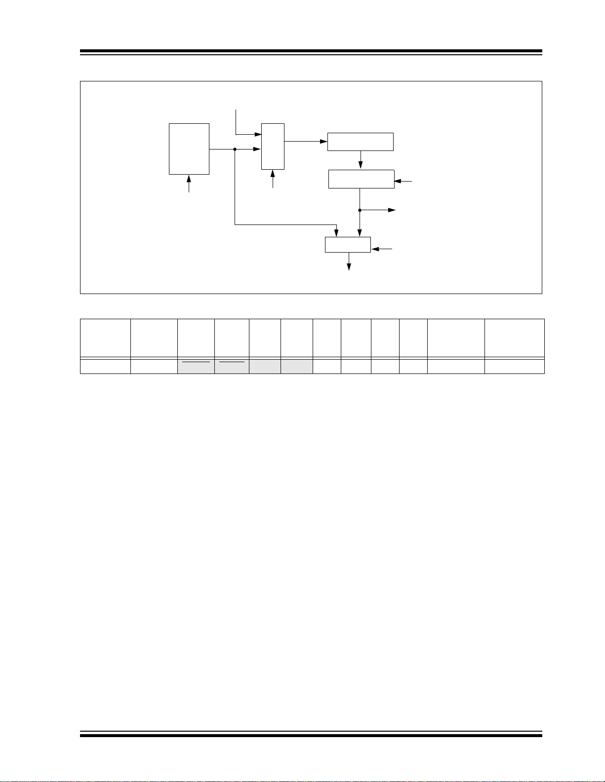
PIC10F200/202/204/206
FIGURE 9-6: WATCHDOG TIMER BLOCK DIAGRAM
From Timer0 Clock Source
(Figure 6-5)
0
M
Watchdog
Time
1
U
X
Postscaler
Postscaler
WDT Enable
Configuration
Bit
PSA
8-to-1 MUX
0
WDT Time-out
1
MUX
PS<2:0>
To Timer0
PSA
(Figure 6-4)
TABLE 9-4: SUMMARY OF REGISTERS ASSOCIATED WITH THE WATCHDOG TIMER
Val u e on
Address Name Bit 7 Bit 6 Bit 5 Bit 4 Bit 3 Bit 2 Bit 1 Bit 0
N/A OPTION
GPWU GPPU T0CS T0SE PSA PS2 PS1 PS0 1111 1111 1111 1111
Legend: Shaded boxes = Not used by Watchdog Timer, – = unimplemented, read as ‘0’, u = unchanged.
Power-On
Reset
Value on
All Other
Resets
© 2007 Microchip Technology Inc. DS41239D-page 47

PIC10F200/202/204/206
9.7 Time-out Sequence, Power-down
and Wake-up from Sleep Status
Bits (TO
The TO, PD, GPWUF and CWUF bits in the STATUS
register can be tested to determine if a Reset condition
has been caused by a power-up condition, a MCLR,
Watchdog Timer (WDT) Reset, wake-up on comparator
change or wake-up on pin change.
TABLE 9-5: TO, PD, GPWUF, CWUF STATUS AFTER RESET
CWUF GPWUF TO PD Reset Caused By
0000WDT wake-up from Sleep
000uWDT time-out (not from Sleep)
0010MCLR
0011Power-up
00uuMCLR
0110Wake-up from Sleep on pin change
1010Wake-up from Sleep on comparator change
Legend: u = unchanged, x = unknown, – = unimplemented bit, read as ‘0’, q = value depends on condition.
Note 1: The TO, PD, GPWUF and CWUF bits maintain their status (u) until a Reset occurs. A low-pulse on the
MCLR
, PD, GPWUF, CWUF)
wake-up from Sleep
not during Sleep
input does not change the TO, PD, GPWUF or CWUF Status bits.
9.8 Reset on Brown-out
A Brown-out Reset is a condition where device power
(V
DD) dips below its minimum value, but not to zero,
and then recovers. The device should be reset in the
event of a brown-out.
To reset PIC10F200/202/204/206 devices when a
Brown-out Reset occurs, external brown-out protection
circuits may be built, as shown in Figure 9-7 and
Figure 9-8.
FIGURE 9-7: BROWN-OUT
PROTECTION CIRCUIT 1
VDD
VDD
33k
Q1
40k
MCLR
(1)
10k
Note 1: This circuit will activate Reset when VDD goes
below Vz + 0.7V (where Vz = Zener voltage).
2: Pin must be confirmed as MCLR
PIC10F20X
(2)
.
FIGURE 9-8: BROWN-OUT
PROTECTION CIRCUIT 2
VDD
VDD
R1
Q1
MCLR
R2
Note 1: This brown-out circuit is less expensive,
although less accurate. Transistor Q1 turns
off when V
that:
V
DD •
2: Pin must be confirmed as MCLR
(1)
40k
DD is below a certain level such
R1
R1 + R2
PIC10F20X
(2)
= 0.7V
.
DS41239D-page 48 © 2007 Microchip Technology Inc.
PIC10F200/202/204/206
FIGURE 9-9: BROWN-OUT
PROTECTION CIRCUIT 3
VDD
MCP809
VSS
RST
Note: This brown-out protection circuit employs
Bypass
Capacitor
VDD
Microchip Technology’s MCP809 microcontroller supervisor. There are 7 different
trip point selections to accommodate 5V to
3V systems.
VDD
MCLR
PIC10F20X
9.9 Power-Down Mode (Sleep)
A device may be powered down (Sleep) and later
powered up (wake-up from Sleep).
9.9.1 SLEEP
The Power-Down mode is entered by executing a
SLEEP instruction.
If enabled, the Watchdog Timer will be cleared but
keeps running, the TO
bit (STATUS<3>) is cleared and the oscillator driver is
turned off. The I/O ports maintain the status they had
before the SLEEP instruction was executed (driving
high, driving low or high-impedance).
bit (STATUS<4>) is set, the PD
9.9.2 WAKE-UP FROM SLEEP
The device can wake-up from Sleep through one of
the following events:
1. An external Reset input on GP3/MCLR
when configured as MCLR
.
2. A Watchdog Timer time-out Reset (if WDT was
enabled).
3. A change on input pin GP0, GP1 or GP3 when
wake-up on change is enabled.
4. A comparator output change has occurred when
wake-up on comparator change is enabled.
These events cause a device Reset. The TO
GPWUF and CWUF bits can be used to determine the
cause of device Reset. The TO
bit is cleared if a WDT
time-out occurred (and caused wake-up). The PD
which is set on power-up, is cleared when SLEEP is
invoked. The GPWUF bit indicates a change in state
while in Sleep at pins GP0, GP1 or GP3 (since the last
file or bit operation on GP port). The CWUF bit
indicates a change in the state while in Sleep of the
comparator output.
Note: Caution: Right before entering Sleep,
read the input pins. When in Sleep, wakeup occurs when the values at the pins
change from the state they were in at the
last reading. If a wake-up on change
occurs and the pins are not read before reentering Sleep, a wake-up will occur
immediately even if no pins change while
in Sleep mode.
/VPP pin,
, PD
bit,
Note: A Reset generated by a WDT time-out
does not drive the MCLR
pin low.
For lowest current consumption while powered down,
the T0CKI input should be at V
MCLR
/VPP pin must be at a logic high level if MCLR is
DD or VSS and the GP3/
enabled.
Note: The WDT is cleared when the device
wakes from Sleep, regardless of the wakeup source.
© 2007 Microchip Technology Inc. DS41239D-page 49

PIC10F200/202/204/206
9.10 Program Verification/Code
Protection
If the code protection bit has not been programmed, the
on-chip program memory can be read out for
verification purposes.
The first 64 locations and the last location (Reset
vector) can be read, regardless of the code protection
bit setting.
9.11 ID Locations
Four memory locations are designated as ID locations
where the user can store checksum or other code
identification numbers. These locations are not
accessible during normal execution, but are readable
and writable during Program/Verify.
Use only the lower 4 bits of the ID locations and always
program the upper 8 bits as ‘0’s.
9.12 In-Circuit Serial Programming™
The PIC10F200/202/204/206 microcontrollers can be
serially programmed while in the end application circuit.
This is simply done with two lines for clock and data,
and three other lines for power, ground and the
programming voltage. This allows customers to manufacture boards with unprogrammed devices and then
program the microcontroller just before shipping the
product. This also allows the most recent firmware or a
custom firmware, to be programmed.
The devices are placed into a Program/Verify mode by
holding the GP1 and GP0 pins low while raising the
(VPP) pin from VIL to VIHH (see programming
MCLR
specification). GP1 becomes the programming clock
and GP0 becomes the programming data. Both GP1
and GP0 are Schmitt Trigger inputs in this mode.
After Reset, a 6-bit command is then supplied to the
device. Depending on the command, 16 bits of program
data are then supplied to or from the device, depending
if the command was a Load or a Read. For complete
details of serial programming, please refer to the
PIC10F200/202/204/206 Programming Specifications.
A typical In-Circuit Serial Programming connection is
shown in Figure 9-10.
FIGURE 9-10: TYPICAL IN-CIRCUIT
SERIAL
PROGRAMMING™
CONNECTION
To N o r m a l
External
Connector
Signals
+5V
0V
PP
V
CLK
Data I/O
Connections
To N o r m a l
Connections
PIC10F20X
DD
V
VSS
MCLR/VPP
GP1
GP0
DD
V
DS41239D-page 50 © 2007 Microchip Technology Inc.
PIC10F200/202/204/206
10.0 INSTRUCTION SET SUMMARY
The PIC16 instruction set is highly orthogonal and is
comprised of three basic categories.
• Byte-oriented operations
• Bit-oriented operations
• Literal and control operations
Each PIC16 instruction is a 12-bit word divided into an
opcode, which specifies the instruction type and one or
more operands which further specify the operation of
the instruction. The formats for each of the categories
is presented in Figure 10-1, while the various opcode
fields are summarized in Table 10-1.
For byte-oriented instructions, ‘f’ represents a file
register designator and ‘d’ represents a destination
designator. The file register designator specifies which
file register is to be used by the instruction.
The destination designator specifies where the result of
the operation is to be placed. If ‘d’ is ‘0’, the result is
placed in the W register. If ‘d’ is ‘1’, the result is placed
in the file register specified in the instruction.
For bit-oriented instructions, ‘b’ represents a bit field
designator which selects the number of the bit affected
by the operation, while ‘f’ represents the number of the
file in which the bit is located.
For literal and control operations, ‘k’ represents an
8 or 9-bit constant or literal value.
All instructions are executed within a single instruction
cycle, unless a conditional test is true or the program
counter is changed as a result of an instruction. In this
case, the execution takes two instruction cycles. One
instruction cycle consists of four oscillator periods.
Thus, for an oscillator frequency of 4 MHz, the normal
instruction execution time is 1 μs. If a conditional test is
true or the program counter is changed as a result of an
instruction, the instruction execution time is 2 μs.
Figure 10-1 shows the three general formats that the
instructions can have. All examples in the figure use
the following format to represent a hexadecimal
number:
0xhhh
where ‘h’ signifies a hexadecimal digit.
FIGURE 10-1: GENERAL FORMAT FOR
INSTRUCTIONS
Byte-oriented file register operations
11 6 5 4 0
OPCODE d f (FILE #)
d = 0 for destination W
d = 1 for destination f
f = 5-bit file register address
Bit-oriented file register operations
11 8 7 5 4 0
OPCODE b (BIT #) f (FILE #)
TABLE 10-1: OPCODE FIELD
DESCRIPTIONS
Field Description
f Register file address (0x00 to 0x7F)
W Working register (accumulator)
b Bit address within an 8-bit file register
k Literal field, constant data or label
x Don’t care location (= 0 or 1)
The assembler will generate code with x = 0. It is
the recommended form of use for compatibility with
all Microchip software tools.
d Destination select;
d = 0 (store result in W)
d = 1 (store result in file register ‘f’)
Default is d = 1
label Label name
TOS Top-of-Stack
PC Program Counter
WDT Watchdog Timer counter
Time-out bit
TO
Power-down bit
PD
dest Destination, either the W register or the specified
[ ] Options
( ) Contents
italics User defined term (font is courier)
register file location
→ Assigned to
< > Register bit field
∈ In the set of
b = 3-bit address
f = 5-bit file register address
Literal and control operations (except GOTO)
11 8 7 0
OPCODE k (literal)
k = 8-bit immediate value
Literal and control operations – GOTO instruction
11 9 8 0
OPCODE k (literal)
k = 9-bit immediate value
© 2007 Microchip Technology Inc. DS41239D-page 51

PIC10F200/202/204/206
TABLE 10-2: INSTRUCTION SET SUMMARY
Mnemonic,
Operands
ADDWF
ANDWF
CLRF
CLRW
COMF
DECF
DECFSZ
INCF
INCFSZ
IORWF
MOVF
MOVWF
NOP
RLF
RRF
SUBWF
SWAPF
XORWF
BCF
BSF
BTFSC
BTFSS
ANDLW
CALL
CLRWDT
GOTO
IORLW
MOVLW
OPTION
RETLW
SLEEP
TRIS
XORLW
Note 1: The 9th bit of the program counter will be forced to a ‘0’ by any instruction that writes to the PC except for
f, d
f, d
f
—
f, d
f, d
f, d
f, d
f, d
f, d
f, d
f
—
f, d
f, d
f, d
f, d
f, d
f, b
f, b
f, b
f, b
k
k
k
k
k
—
k
—
f
k
GOTO. See Section 4.7 “Program Counter”.
2: When an I/O register is modified as a function of itself (e.g. MOVF PORTB, 1), the value used will be that
value present on the pins themselves. For example, if the data latch is ‘1’ for a pin configured as input and
is driven low by an external device, the data will be written back with a ‘0’.
3: The instruction TRIS f, where f = 6, causes the contents of the W register to be written to the tri-state
latches of PORTB. A ‘1’ forces the pin to a high-impedance state and disables the output buffers.
4: If this instruction is executed on the TMR0 register (and where applicable, d = 1), the prescaler will be
cleared (if assigned to TMR0).
Add W and f
AND W with f
Clear f
Clear W
Complement f
Decrement f
Decrement f, Skip if 0
Increment f
Increment f, Skip if 0
Inclusive OR W with f
Move f
Move W to f
No Operation
Rotate left f through Carry
Rotate right f through Carry
Subtract W from f
Swap f
Exclusive OR W with f
Bit Clear f
Bit Set f
Bit Test f, Skip if Clear
Bit Test f, Skip if Set
AND literal with W
Call Subroutine
Clear Watchdog Timer
Unconditional branch
Inclusive OR literal with W
Move literal to W
Load OPTION register
Return, place Literal in W
Go into Standby mode
Load TRIS register
Exclusive OR literal to W
Description Cycles
1
1
1
1
1
1
(2)
1
1
(2)
1
1
1
1
1
1
1
1
1
1
BIT-ORIENTED FILE REGISTER OPERATIONS
1
1
(2)
1
(2)
1
LITERAL AND CONTROL OPERATIONS
1
2
1
2
1
1
1
2
1
1
1
12-Bit Opcode
MSb LSb
0001
0001
0000
0000
0010
0000
0010
0010
0011
0001
0010
0000
0000
0011
0011
0000
0011
0001
0100
0101
0110
0111
1110
1001
0000
101k
1101
1100
0000
1000
0000
0000
1111
11df
01df
011f
0100
01df
11df
11df
10df
11df
00df
00df
001f
0000
01df
00df
10df
10df
10df
bbbf
bbbf
bbbf
bbbf
kkkk
kkkk
0000
kkkk
kkkk
kkkk
0000
kkkk
0000
0000
kkkk
ffff
ffff
ffff
0000
ffff
ffff
ffff
ffff
ffff
ffff
ffff
ffff
0000
ffff
ffff
ffff
ffff
ffff
ffff
ffff
ffff
ffff
kkkk
kkkk
0100
kkkk
kkkk
kkkk
0010
kkkk
0011
0fff
kkkk
Status
Affected
C, DC, Z
Z
Z
Z
Z
Z
None
Z
None
Z
Z
None
None
C
C
C, DC, Z
None
Z
None
None
None
None
Z
None
, PD
TO
None
Z
None
None
None
, PD
TO
None
Z
Notes
1, 2, 4
2, 4
4
2, 4
2, 4
2, 4
2, 4
2, 4
2, 4
1, 4
2, 4
2, 4
1, 2, 4
2, 4
2, 4
2, 4
2, 4
1
3
DS41239D-page 52 © 2007 Microchip Technology Inc.

PIC10F200/202/204/206
ADDWF Add W and f
Syntax: [ label ] ADDWF f,d
Operands: 0 ≤ f ≤ 31
d ∈ [0,1]
Operation: (W) + (f) → (dest)
Status Affected: C, DC, Z
Description: Add the contents of the W register
and register ‘f’. If ‘d’ is ‘0’, the result
is stored in the W register. If ‘d’ is
‘1’, the result is stored back in
register ‘f’.
ANDLW AND literal with W
Syntax: [ label ] ANDLW k
Operands: 0 ≤ k ≤ 255
Operation: (W).AND. (k) → (W)
Status Affected: Z
Description: The contents of the W register are
AND’ed with the eight-bit literal ‘k’.
The result is placed in the W
register.
BCF Bit Clear f
Syntax: [ label ] BCF f,b
Operands: 0 ≤ f ≤ 31
0 ≤ b ≤ 7
Operation: 0 → (f<b>)
Status Affected: None
Description: Bit ‘b’ in register ‘f’ is cleared.
BSF Bit Set f
Syntax: [ label ] BSF f,b
Operands: 0 ≤ f ≤ 31
0 ≤ b ≤ 7
Operation: 1 → (f<b>)
Status Affected: None
Description: Bit ‘b’ in register ‘f’ is set.
ANDWF AND W with f
Syntax: [ label ] ANDWF f,d
Operands: 0 ≤ f ≤ 31
d ∈ [0,1]
Operation: (W) .AND. (f) → (dest)
Status Affected: Z
Description: The contents of the W register are
AND’ed with register ‘f’. If ‘d’ is ‘0’,
the result is stored in the W register.
If ‘d’ is ‘1’, the result is stored back
in register ‘f’.
BTFSC Bit Test f, Skip if Clear
Syntax: [ label ] BTFSC f,b
Operands: 0 ≤ f ≤ 31
0 ≤ b ≤ 7
Operation: skip if (f<b>) = 0
Status Affected: None
Description: If bit ‘b’ in register ‘f’ is ‘0’, then the
next instruction is skipped.
If bit ‘b’ is ‘0’, then the next instruc-
tion fetched during the current
instruction execution is discarded,
and a NOP is executed instead,
making this a two-cycle instruction.
© 2007 Microchip Technology Inc. DS41239D-page 53

PIC10F200/202/204/206
BTFSS Bit Test f, Skip if Set
Syntax: [ label ] BTFSS f,b
Operands: 0 ≤ f ≤ 31
0 ≤ b < 7
Operation: skip if (f<b>) = 1
Status Affected: None
Description: If bit ‘b’ in register ‘f’ is ‘1’, then the
next instruction is skipped.
If bit ‘b’ is ‘1’, then the next instruc-
tion fetched during the current
instruction execution, is discarded
and a NOP is executed instead,
making this a two-cycle instruction.
CALL Subroutine Call
Syntax: [ label ] CALL k
Operands: 0 ≤ k ≤ 255
Operation: (PC) + 1→ Top-of-Stack;
k → PC<7:0>;
(STATUS<6:5>) → PC<10:9>;
0 → PC<8>
Status Affected: None
Description: Subroutine call. First, return
address (PC + 1) is PUSHed onto
the stack. The eight-bit immediate
address is loaded into PC
bits <7:0>. The upper bits
PC<10:9> are loaded from
STATUS<6:5>, PC<8> is cleared.
CALL is a two-cycle instruction.
CLRW Clear W
Syntax: [ label ] CLRW
Operands: None
Operation: 00h → (W);
1 → Z
Status Affected: Z
Description: The W register is cleared. Zero bit
(Z) is set.
CLRWDT Clear Watchdog Timer
Syntax: [ label ] CLRWDT
Operands: None
Operation: 00h → WDT;
0 → WDT prescaler (if assigned);
1 → TO;
1 → PD
Status Affected: TO, PD
Description: The CLRWDT instruction resets the
WDT. It also resets the prescaler, if
the prescaler is assigned to the
WDT and not Timer0. Status bits
TO and PD are set.
CLRF Clear f
Syntax: [ label ] CLRF f
Operands: 0 ≤ f ≤ 31
Operation: 00h → (f);
1 → Z
Status Affected: Z
Description: The contents of register ‘f’ are
cleared and the Z bit is set.
DS41239D-page 54 © 2007 Microchip Technology Inc.
COMF Complement f
Syntax: [ label ] COMF f,d
Operands: 0 ≤ f ≤ 31
d ∈ [0,1]
Operation: (f
Status Affected: Z
Description: The contents of register ‘f’ are
) → (dest)
complemented. If ‘d’ is ‘0’, the
result is stored in the W register. If
‘d’ is ‘1’, the result is stored back in
register ‘f’.

PIC10F200/202/204/206
DECF Decrement f
Syntax: [ label ] DECF f,d
Operands: 0 ≤ f ≤ 31
d ∈ [0,1]
Operation: (f) – 1 → (dest)
Status Affected: Z
Description: Decrement register ‘f’. If ‘d’ is ‘0’,
the result is stored in the W
register. If ‘d’ is ‘1’, the result is
stored back in register ‘f’.
DECFSZ Decrement f, Skip if 0
Syntax: [ label ] DECFSZ f,d
Operands: 0 ≤ f ≤ 31
d ∈ [0,1]
Operation: (f) – 1 → d; skip if result = 0
Status Affected: None
Description: The contents of register ‘f’ are
decremented. If ‘d’ is ‘0’, the result
is placed in the W register. If ‘d’ is
‘1’, the result is placed back in
register ‘f’.
If the result is ‘0’, the next instruction, which is already fetched, is
discarded and a NOP is executed
instead making it a two-cycle
instruction.
INCF Increment f
Syntax: [ label ] INCF f,d
Operands: 0 ≤ f ≤ 31
d ∈ [0,1]
Operation: (f) + 1 → (dest)
Status Affected: Z
Description: The contents of register ‘f’ are
incremented. If ‘d’ is ‘0’, the result
is placed in the W register. If ‘d’ is
‘1’, the result is placed back in
register ‘f’.
INCFSZ Increment f, Skip if 0
Syntax: [ label ] INCFSZ f,d
Operands: 0 ≤ f ≤ 31
d ∈ [0,1]
Operation: (f) + 1 → (dest), skip if result = 0
Status Affected: None
Description: The contents of register ‘f’ are
incremented. If ‘d’ is ‘0’, the result
is placed in the W register. If ‘d’ is
‘1’, the result is placed back in
register ‘f’.
If the result is ‘0’, then the next
instruction, which is already
fetched, is discarded and a NOP is
executed instead making it a
two-cycle instruction.
GOTO Unconditional Branch
Syntax: [ label ] GOTO k
Operands: 0 ≤ k ≤ 511
Operation: k → PC<8:0>;
STATUS<6:5> → PC<10:9>
Status Affected: None
Description: GOTO is an unconditional branch.
The 9-bit immediate value is
loaded into PC bits <8:0>. The
upper bits of PC are loaded from
STATUS<6:5>. GOTO is a twocycle instruction.
© 2007 Microchip Technology Inc. DS41239D-page 55
IORLW Inclusive OR literal with W
Syntax: [ label ] IORLW k
Operands: 0 ≤ k ≤ 255
Operation: (W) .OR. (k) → (W)
Status Affected: Z
Description: The contents of the W register are
OR’ed with the eight-bit literal ‘k’.
The result is placed in the W
register.

PIC10F200/202/204/206
IORWF Inclusive OR W with f
Syntax: [ label ] IORWF f,d
Operands: 0 ≤ f ≤ 31
d ∈ [0,1]
Operation: (W).OR. (f) → (dest)
Status Affected: Z
Description: Inclusive OR the W register with
register ‘f’. If ‘d’ is ‘0’, the result is
placed in the W register. If ‘d’ is ‘1’,
the result is placed back in register
‘f’.
MOVF Move f
Syntax: [ label ] MOVF f,d
Operands: 0 ≤ f ≤ 31
d ∈ [0,1]
Operation: (f) → (dest)
Status Affected: Z
Description: The contents of register ‘f’ are
moved to destination ‘d’. If ‘d’ is ‘0’,
destination is the W register. If ‘d’
is ‘1’, the destination is file
register ‘f’. ‘d’ = 1 is useful as a
test of a file register, since status
flag Z is affected.
MOVWF Move W to f
Syntax: [ label ] MOVWF f
Operands: 0 ≤ f ≤ 31
Operation: (W) → (f)
Status Affected: None
Description: Move data from the W register to
register ‘f’.
NOP No Operation
Syntax: [ label ] NOP
Operands: None
Operation: No operation
Status Affected: None
Description: No operation.
MOVLW Move literal to W
Syntax: [ label ] MOVLW k
Operands: 0 ≤ k ≤ 255
Operation: k → (W)
Status Affected: None
Description: The eight-bit literal ‘k’ is loaded
into the W register. The “don’t
cares” will assembled as ‘0’s.
OPTION Load OPTION Register
Syntax: [ label ] OPTION
Operands: None
Operation: (W) → Option
Status Affected: None
Description: The content of the W register is
loaded into the OPTION register.
DS41239D-page 56 © 2007 Microchip Technology Inc.

PIC10F200/202/204/206
RETLW Return with literal in W
Syntax: [ label ] RETLW k
Operands: 0 ≤ k ≤ 255
Operation: k → (W);
TOS → PC
Status Affected: None
Description: The W register is loaded with the
eight-bit literal ‘k’. The program
counter is loaded from the top of
the stack (the return address). This
is a two-cycle instruction.
RLF Rotate Left f through Carry
Syntax: [ label ] RLF f,d
Operands: 0 ≤ f ≤ 31
d ∈ [0,1]
Operation: See description below
Status Affected: C
Description: The contents of register ‘f’ are
rotated one bit to the left through
the Carry flag. If ‘d’ is ‘0’, the result
is placed in the W register. If ‘d’ is
‘1’, the result is stored back in
register ‘f’.
C
register ‘f’
SLEEP Enter SLEEP Mode
Syntax:
Operands: None
Operation: 00h → WDT;
Status Affected: TO, PD, RBWUF
Description: Time-out Status bit (TO
SUBWF Subtract W from f
Syntax:
Operands: 0 ≤ f ≤ 31
Operation: (f) – (W) → (dest)
Status Affected: C, DC, Z
Description: Subtract (2’s complement method)
[ label ]
0 → WDT prescaler;
1 → TO
0 → PD
Power-down Status bit (PD
cleared.
RBWUF is unaffected.
The WDT and its prescaler are
cleared.
The processor is put into Sleep
mode with the oscillator stopped.
See Section 9.9 “Power-Down
Mode (Sleep)” for more details.
[ label ] SUBWF f,d
d ∈ [0,1]
the W register from register ‘f’. If ‘d’
is ‘0’, the result is stored in the W
register. If ‘d’ is ‘1’, the result is
stored back in register ‘f’.
SLEEP
;
) is set. The
) is
RRF Rotate Right f through Carry
Syntax: [ label ] RRF f,d
Operands: 0 ≤ f ≤ 31
d ∈ [0,1]
Operation: See description below
Status Affected: C
Description: The contents of register ‘f’ are
rotated one bit to the right through
the Carry flag. If ‘d’ is ‘0’, the result
is placed in the W register. If ‘d’ is
‘1’, the result is placed back in
register ‘f’.
C
© 2007 Microchip Technology Inc. DS41239D-page 57
register ‘f’
SWAPF Swap Nibbles in f
Syntax: [ label ] SWAPF f,d
Operands: 0 ≤ f ≤ 31
d ∈ [0,1]
Operation: (f<3:0>) → (dest<7:4>);
(f<7:4>) → (dest<3:0>)
Status Affected: None
Description: The upper and lower nibbles of
register ‘f’ are exchanged. If ‘d’ is
‘0’, the result is placed in W
register. If ‘d’ is ‘1’, the result is
placed in register ‘f’.

PIC10F200/202/204/206
TRIS Load TRIS Register
Syntax: [ label ] TRIS f
Operands: f =
Operation: (W) → TRIS register f
Status Affected: None
Description: TRIS register ‘f’ (f = 6 or 7) is
XORLW Exclusive OR literal with W
Syntax:
Operands: 0 ≤ k ≤ 255
Operation: (W) .XOR. k → (W)
Status Affected: Z
Description: The contents of the W register are
6
loaded with the contents of the W
register
[ label ]XORLW k
XOR’ed with the eight-bit literal ‘k’.
The result is placed in the W
register.
XORWF Exclusive OR W with f
Syntax: [ label ] XORWF f,d
Operands: 0 ≤ f ≤ 31
d ∈ [0,1]
Operation: (W) .XOR. (f) → (dest)
Status Affected: Z
Description: Exclusive OR the contents of the
W register with register ‘f’. If ‘d’ is
‘0’, the result is stored in the W
register. If ‘d’ is ‘1’, the result is
stored back in register ‘f’.
DS41239D-page 58 © 2007 Microchip Technology Inc.

PIC10F200/202/204/206
11.0 DEVELOPMENT SUPPORT
The PIC® microcontrollers are supported with a full
range of hardware and software development tools:
• Integrated Development Environment
- MPLAB
• Assemblers/Compilers/Linkers
- MPASM
- MPLAB C18 and MPLAB C30 C Compilers
-MPLINK
MPLIB
- MPLAB ASM30 Assembler/Linker/Library
• Simulators
- MPLAB SIM Software Simulator
•Emulators
- MPLAB ICE 2000 In-Circuit Emulator
- MPLAB ICE 4000 In-Circuit Emulator
• In-Circuit Debugger
- MPLAB ICD 2
• Device Programmers
- PICSTART
- MPLAB PM3 Device Programmer
- PICkit™ 2 Development Programmer
• Low-Cost Demonstration and Development
Boards and Evaluation Kits
®
IDE Software
TM
Assembler
TM
Object Linker/
TM
Object Librarian
®
Plus Development Programmer
11.1 MPLAB Integrated Development
Environment Software
The MPLAB IDE software brings an ease of software
development previously unseen in the 8/16-bit microcontroller market. The MPLAB IDE is a Windows
operating system-based application that contains:
• A single graphical interface to all debugging tools
- Simulator
- Programmer (sold separately)
- Emulator (sold separately)
- In-Circuit Debugger (sold separately)
• A full-featured editor with color-coded context
• A multiple project manager
• Customizable data windows with direct edit of
contents
• High-level source code debugging
• Visual device initializer for easy register
initialization
• Mouse over variable inspection
• Drag and drop variables from source to watch
windows
• Extensive on-line help
• Integration of select third party tools, such as
HI-TECH Software C Compilers and IAR
C Compilers
The MPLAB IDE allows you to:
• Edit your source files (either assembly or C)
• One touch assemble (or compile) and download
to PIC MCU emulator and simulator tools
(automatically updates all project information)
• Debug using:
- Source files (assembly or C)
- Mixed assembly and C
- Machine code
MPLAB IDE supports multiple debugging tools in a
single development paradigm, from the cost-effective
simulators, through low-cost in-circuit debuggers, to
full-featured emulators. This eliminates the learning
curve when upgrading to tools with increased flexibility
and power.
®
© 2007 Microchip Technology Inc. DS41239D-page 59

PIC10F200/202/204/206
11.2 MPASM Assembler
The MPASM Assembler is a full-featured, universal
macro assembler for all PIC MCUs.
The MPASM Assembler generates relocatable object
files for the MPLINK Object Linker, Intel
files, MAP files to detail memory usage and symbol
reference, absolute LST files that contain source lines
and generated machine code and COFF files for
debugging.
The MPASM Assembler features include:
• Integration into MPLAB IDE projects
• User-defined macros to streamline
assembly code
• Conditional assembly for multi-purpose
source files
• Directives that allow complete control over the
assembly process
®
standard HEX
11.3 MPLAB C18 and MPLAB C30
C Compilers
The MPLAB C18 and MPLAB C30 Code Development
Systems are complete ANSI C compilers for
Microchip’s PIC18 family of microcontrollers and the
dsPIC30, dsPIC33 and PIC24 family of digital signal
controllers. These compilers provide powerful integration capabilities, superior code optimization and ease
of use not found with other compilers.
For easy source level debugging, the compilers provide
symbol information that is optimized to the MPLAB IDE
debugger.
11.4 MPLINK Object Linker/
MPLIB Object Librarian
The MPLINK Object Linker combines relocatable
objects created by the MPASM Assembler and the
MPLAB C18 C Compiler. It can link relocatable objects
from precompiled libraries, using directives from a
linker script.
The MPLIB Object Librarian manages the creation and
modification of library files of precompiled code. When
a routine from a library is called from a source file, only
the modules that contain that routine will be linked in
with the application. This allows large libraries to be
used efficiently in many different applications.
The object linker/library features include:
• Efficient linking of single libraries instead of many
smaller files
• Enhanced code maintainability by grouping
related modules together
• Flexible creation of libraries with easy module
listing, replacement, deletion and extraction
11.5 MPLAB ASM30 Assembler, Linker
and Librarian
MPLAB ASM30 Assembler produces relocatable
machine code from symbolic assembly language for
dsPIC30F devices. MPLAB C30 C Compiler uses the
assembler to produce its object file. The assembler
generates relocatable object files that can then be
archived or linked with other relocatable object files and
archives to create an executable file. Notable features
of the assembler include:
• Support for the entire dsPIC30F instruction set
• Support for fixed-point and floating-point data
• Command line interface
• Rich directive set
• Flexible macro language
• MPLAB IDE compatibility
11.6 MPLAB SIM Software Simulator
The MPLAB SIM Software Simulator allows code
development in a PC-hosted environment by simulating the PIC MCUs and dsPIC® DSCs on an instruction
level. On any given instruction, the data areas can be
examined or modified and stimuli can be applied from
a comprehensive stimulus controller. Registers can be
logged to files for further run-time analysis. The trace
buffer and logic analyzer display extend the power of
the simulator to record and track program execution,
actions on I/O, most peripherals and internal registers.
The MPLAB SIM Software Simulator fully supports
symbolic debugging using the MPLAB C18 and
MPLAB C30 C Compilers, and the MPASM and
MPLAB ASM30 Assemblers. The software simulator
offers the flexibility to develop and debug code outside
of the hardware laboratory environment, making it an
excellent, economical software development tool.
DS41239D-page 60 © 2007 Microchip Technology Inc.

PIC10F200/202/204/206
11.7 MPLAB ICE 2000
High-Performance
In-Circuit Emulator
The MPLAB ICE 2000 In-Circuit Emulator is intended
to provide the product development engineer with a
complete microcontroller design tool set for PIC microcontrollers. Software control of the MPLAB ICE 2000
In-Circuit Emulator is advanced by the MPLAB Integrated Development Environment, which allows editing, building, downloading and source debugging from
a single environment.
The MPLAB ICE 2000 is a full-featured emulator
system with enhanced trace, trigger and data monitoring features. Interchangeable processor modules allow
the system to be easily reconfigured for emulation of
different processors. The architecture of the MPLAB
ICE 2000 In-Circuit Emulator allows expansion to
support new PIC microcontrollers.
The MPLAB ICE 2000 In-Circuit Emulator system has
been designed as a real-time emulation system with
advanced features that are typically found on more
expensive development tools. The PC platform and
Microsoft
chosen to best make these features available in a
simple, unified application.
®
Windows® 32-bit operating system were
11.8 MPLAB ICE 4000
High-Performance
In-Circuit Emulator
The MPLAB ICE 4000 In-Circuit Emulator is intended to
provide the product development engineer with a
complete microcontroller design tool set for high-end
PIC MCUs and dsPIC DSCs. Software control of the
MPLAB ICE 4000 In-Circuit Emulator is provided by the
MPLAB Integrated Development Environment, which
allows editing, building, downloading and source
debugging from a single environment.
The MPLAB ICE 4000 is a premium emulator system,
providing the features of MPLAB ICE 2000, but with
increased emulation memory and high-speed performance for dsPIC30F and PIC18XXXX devices. Its
advanced emulator features include complex triggering
and timing, and up to 2 Mb of emulation memory.
The MPLAB ICE 4000 In-Circuit Emulator system has
been designed as a real-time emulation system with
advanced features that are typically found on more
expensive development tools. The PC platform and
Microsoft Windows 32-bit operating system were
chosen to best make these features available in a
simple, unified application.
11.9 MPLAB ICD 2 In-Circuit Debugger
Microchip’s In-Circuit Debugger, MPLAB ICD 2, is a
powerful, low-cost, run-time development tool,
connecting to the host PC via an RS-232 or high-speed
USB interface. This tool is based on the Flash PIC
MCUs and can be used to develop for these and other
PIC MCUs and dsPIC DSCs. The MPLAB ICD 2 utilizes
the in-circuit debugging capability built into the Flash
devices. This feature, along with Microchip’s In-Circuit
Serial Programming
effective, in-circuit Flash debugging from the graphical
user interface of the MPLAB Integrated Development
Environment. This enables a designer to develop and
debug source code by setting breakpoints, single stepping and watching variables, and CPU status and
peripheral registers. Running at full speed enables
testing hardware and applications in real time. MPLAB
ICD 2 also serves as a development programmer for
selected PIC devices.
TM
(ICSPTM) protocol, offers cost-
11.10 MPLAB PM3 Device Programmer
The MPLAB PM3 Device Programmer is a universal,
CE compliant device programmer with programmable
voltage verification at VDDMIN and VDDMAX for
maximum reliability. It features a large LCD display
(128 x 64) for menus and error messages and a modular, detachable socket assembly to support various
package types. The ICSP™ cable assembly is included
as a standard item. In Stand-Alone mode, the MPLAB
PM3 Device Programmer can read, verify and program
PIC devices without a PC connection. It can also set
code protection in this mode. The MPLAB PM3
connects to the host PC via an RS-232 or USB cable.
The MPLAB PM3 has high-speed communications and
optimized algorithms for quick programming of large
memory devices and incorporates an SD/MMC card for
file storage and secure data applications.
© 2007 Microchip Technology Inc. DS41239D-page 61

PIC10F200/202/204/206
11.11 PICSTART Plus Development
Programmer
The PICSTART Plus Development Programmer is an
easy-to-use, low-cost, prototype programmer. It
connects to the PC via a COM (RS-232) port. MPLAB
Integrated Development Environment software makes
using the programmer simple and efficient. The
PICSTART Plus Development Programmer supports
most PIC devices in DIP packages up to 40 pins.
Larger pin count devices, such as the PIC16C92X and
PIC17C76X, may be supported with an adapter socket.
The PICSTART Plus Development Programmer is CE
compliant.
11.12 PICkit 2 Development Programmer
The PICkit™ 2 Development Programmer is a low-cost
programmer with an easy-to-use interface for programming many of Microchip’s baseline, mid-range
and PIC18F families of Flash memory microcontrollers.
The PICkit 2 Starter Kit includes a prototyping development board, twelve sequential lessons, software and
HI-TECH’s PICC™ Lite C compiler, and is designed to
help get up to speed quickly using PIC
controllers. The kit provides everything needed to
program, evaluate and develop applications using
Microchip’s powerful, mid-range Flash memory family
of microcontrollers.
®
micro-
11.13 Demonstration, Development and
Evaluation Boards
A wide variety of demonstration, development and
evaluation boards for various PIC MCUs and dsPIC
DSCs allows quick application development on fully functional systems. Most boards include prototyping areas for
adding custom circuitry and provide application firmware
and source code for examination and modification.
The boards support a variety of features, including LEDs,
temperature sensors, switches, speakers, RS-232
interfaces, LCD displays, potentiometers and additional
EEPROM memory.
The demonstration and development boards can be
used in teaching environments, for prototyping custom
circuits and for learning about various microcontroller
applications.
In addition to the PICDEM™ and dsPICDEM™ demonstration/development board series of circuits, Microchip
has a line of evaluation kits and demonstration software
for analog filter design, K
®
, PowerSmart® battery management, SEEVAL
IrDA
evaluation system, Sigma-Delta ADC, flow rate
sensing, plus many more.
Check the Microchip web page (www.microchip.com)
and the latest “Product Selector Guide” (DS00148) for
the complete list of demonstration, development and
evaluation kits.
EELOQ
®
security ICs, CAN,
®
DS41239D-page 62 © 2007 Microchip Technology Inc.

12.0 ELECTRICAL CHARACTERISTICS
PIC10F200/202/204/206
Absolute Maximum Ratings
(†)
Ambient temperature under bias..........................................................................................................-40°C to +125°C
Storage temperature ............................................................................................................................-65°C to +150°C
Voltage on V
Voltage on MCLR
Voltage on all other pins with respect to V
Total power dissipation
Max. current out of V
Max. current into V
Input clamp current, I
Output clamp current, I
DD with respect to VSS ...............................................................................................................0 to +6.5V
with respect to VSS..........................................................................................................0 to +13.5V
SS ............................................................................... -0.3V to (VDD + 0.3V)
(1)
.................................................................................................................................. 800 mW
SS pin ..................................................................................................................................80 mA
DD pin ..................................................................................................................................... 80 mA
IK (VI < 0 or VI > VDD) ...................................................................................................................±20 mA
OK (VO < 0 or VO > VDD) ...........................................................................................................±20 mA
Max. output current sunk by any I/O pin ..............................................................................................................25 mA
Max. output current sourced by any I/O pin......................................................................................................... 25 mA
Max. output current sourced by I/O port .............................................................................................................. 75 mA
Max. output current sunk by I/O port ................................................................................................................... 75 mA
Note 1: Power dissipation is calculated as follows: P
†
NOTICE: Stresses above those listed under “Absolute Maximum Ratings” may cause permanent damage to the
DIS = VDD x {IDD – ∑ IOH} + ∑ {(VDD – VOH) x IOH} + ∑(VOL x IOL)
device. This is a stress rating only and functional operation of the device at those or any other conditions above
those indicated in the operation listings of this specification is not implied. Exposure to maximum rating conditions
for extended periods may affect device reliability.
© 2007 Microchip Technology Inc. DS41239D-page 63

PIC10F200/202/204/206
FIGURE 12-1: PIC10F200/202/204/206 VOLTAGE-FREQUENCY GRAPH, -40°C ≤ TA ≤ +125°C
6.0
5.5
5.0
4.5
DD
V
(Volts)
4.0
3.5
3.0
2.5
2.0
0
410
Frequency (MHz)
20
25
DS41239D-page 64 © 2007 Microchip Technology Inc.

PIC10F200/202/204/206
12.1 DC Characteristics: PIC10F200/202/204/206 (Industrial)
DC CHARACTERISTICS
Param
D001 V
D002 V
D003 V
Sym Characteristic Min Typ
No.
DD Supply Voltage 2.0 5.5 V See Figure 12-1
DR RAM Data Retention Voltage
POR VDD Start Voltage
Standard Operating Conditions (unless otherwise specified)
Operating Temperature -40×C ≤ T
(1)
(2)
1.5* — — V Device in Sleep mode
Max Units Conditions
A ≤ +85°C (industrial)
—Vss— V
to ensure Power-on Reset
D004 S
VDD VDD Rise Rate
0.05* — — V/ms
to ensure Power-on Reset)
DD Supply Current
I
D010 ——175
PD Power-down Current
I
D020 ——0.1
WDT WDT Current
I
D022 ——1.0
CMP Comparator Current
I
D023 —
VREF Internal Reference Current
I
D024 — 85
(3)
275
0.63
(4)
0.35
(5)
7
(5)
12
—
(5), (6)
44
115
175
195μAμA
μAmAVDD = 2.0V
1.1
1.2
2.4μAμA
3
16μAμA
V
DD = 5.0V
VDD = 2.0V
V
DD = 5.0V
VDD = 2.0V
V
DD = 5.0V
2380μAμAVDD = 2.0V
V
DD = 5.0V
VDD = 2.0V.
V
DD = 5.0V
* These parameters are characterized but not tested.
Note 1: Data in the Typical (“Typ”) column is based on characterization results at 25°C. This data is for design guidance only
and is not tested.
2: This is the limit to which V
DD can be lowered in Sleep mode without losing RAM data.
3: The supply current is mainly a function of the operating voltage and frequency. Other factors such as bus loading, bus
rate, internal code execution pattern and temperature also have an impact on the current consumption.
a) The test conditions for all I
All I/O pins tri-stated, pulled to V
DD measurements in active operation mode are:
SS, T0CKI = VDD, MCLR = VDD; WDT enabled/disabled as specified.
b) For standby current measurements, the conditions are the same, except that the device is in Sleep mode.
4: Power-down current is measured with the part in Sleep mode, with all I/O pins in high-impedance state and tied to V
SS.
or V
5: The peripheral current is the sum of the base I
DD or IPD and the additional current consumed when this peripheral is
enabled.
6: Measured with the comparator enabled.
DD
© 2007 Microchip Technology Inc. DS41239D-page 65
PIC10F200/202/204/206
12.2 DC Characteristics: PIC10F200/202/204/206 (Extended)
DC CHARACTERISTICS
Param
No.
D001 V
D002 V
D003 V
Sym Characteristic Min Typ
DD Supply Voltage 2.0 5.5 V See Figure 12-1
DR RAM Data Retention Voltage
POR VDD Start Voltage
Standard Operating Conditions (unless otherwise specified)
Operating Temperature -40×C £ T
(1)
Max Units Conditions
(2)
1.5* — V Device in Sleep mode
A £ +125×C (extended)
—Vss— V
to ensure Power-on Reset
D004 S
VDD VDD Rise Rate
0.05* — — V/ms
to ensure Power-on Reset
DD Supply Current
I
D010 ——175
PD Power-down Current
I
D020 —
WDT WDT Current
I
D022 —
CMP Comparator Current
I
D023 —
VREF Internal Reference Current
D024 — 85
(3)
275
(4)
0.63
1.1
0.1
—
(5)
0.35915
1.0718
(5)
—
—
(5), (6)
12
42
22
27
85
120
175
200μAμA
μAmAVDD = 2.0V
V
DD = 5.0V
μAμAVDD = 2.0V
V
DD = 5.0V
μAμAVDD = 2.0V
V
DD = 5.0V
μAμAVDD = 2.0V
V
DD = 5.0
VDD = 2.0V
V
DD = 5.0V
* These parameters are characterized but not tested.
Note 1: Data in the Typical (“Typ”) column is based on characterization results at 25°C. This data is for design guidance only
and is not tested.
2: This is the limit to which V
DD can be lowered in Sleep mode without losing RAM data.
3: The supply current is mainly a function of the operating voltage and frequency. Other factors such as bus loading, bus
rate, internal code execution pattern and temperature also have an impact on the current consumption.
a) The test conditions for all I
All I/O pins tri-stated, pulled to V
DD measurements in active operation mode are:
SS, T0CKI = VDD, MCLR = VDD; WDT enabled/disabled as specified.
b) For standby current measurements, the conditions are the same, except that the device is in Sleep mode.
4: Power-down current is measured with the part in Sleep mode, with all I/O pins in high-impedance state and tied to V
SS.
or V
5: The peripheral current is the sum of the base I
DD or IPD and the additional current consumed when this peripheral is
enabled.
6: Measured with the Comparator enabled.
DD
DS41239D-page 66 © 2007 Microchip Technology Inc.
PIC10F200/202/204/206
12.3 DC Characteristics: PIC10F200/202/204/206 (Industrial, Extended)
Standard Operating Conditions (unless otherwise specified)
DC CHARACTERISTICS
Param
Sym Characteristic Min Typ† Max Units Conditions
No.
V
IL Input Low Voltage
Operating temperature -40°C ≤ T
-40°C ≤ T
Operating voltage V
DD range as described in DC specification
I/O ports:
D030 with TTL buffer Vss — 0.8 V For all 4.5 ≤ V
D030A Vss — 0.15 V
D031 with Schmitt Trigger
Vss — 0.2 V
buffer
D032 MCLR
IH Input High Voltage
V
, T0CKI Vss — 0.2 VDD V
I/O ports: —
D040 with TTL buffer 2.0 — V
D040A 0.25 V
D041 with Schmitt Trigger
DD + 0.8 — VDD V Otherwise
DD —VDD V For entire VDD range
0.8V
DD V4.5 ≤ VDD ≤ 5.5V
buffer
D042 MCLR
D070 I
PUR GPIO weak pull-up current
IIL Input Leakage Current
, T0CKI 0.8VDD —VDD V
(3)
(1, 2)
50 250 400 μAVDD = 5V, VPIN = VSS
D060 I/O ports — ±0.1 ± 1 μAVss ≤ VPIN ≤ VDD, Pin at high-imped-
D061 GP3/MCLR
(4)
—±0.7± 5μAVss ≤ VPIN ≤ VDD
Output Low Voltage
D080 I/O ports — — 0.6 V I
D080A — — 0.6 V I
Output High Voltage
D090 I/O ports
(2)
D090A V
VDD – 0.7 — — V IOH = -3.0 mA, VDD = 4.5V, -40°C to
DD – 0.7 — — V IOH = -2.5 mA, VDD = 4.5V, -40°C to
Capacitive Loading Specs on Output Pins
D101 All I/O pins — — 50* pF
† Data in “Typ” column is at 5V, 25°C unless otherwise stated. These parameters are for design guidance only and are not
tested.
* These parameters are for design guidance only and are not tested.
Note 1: The leakage current on the MCLR
pin is strongly dependent on the applied voltage level. The specified levels represent
normal operating conditions. Higher leakage current may be measured at different input voltages.
2: Negative current is defined as coming out of the pin.
3: This specification applies when GP3/MCLR
circuit is higher than the standard I/O logic.
MCLR
is configured as an input with pull-up disabled. The leakage current of the
A ≤ +85°C (industrial)
A ≤ +125°C (extended)
DD ≤ 5.5V
DD V Otherwise
DD V
ance
OL = 8.5 mA, VDD = 4.5V, -40°C to
+85°C
OL = 7.0 mA, VDD = 4.5V, -40°C to
+125°C
+85°C
+125°C
© 2007 Microchip Technology Inc. DS41239D-page 67

PIC10F200/202/204/206
TABLE 12-1: COMPARATOR SPECIFICATIONS
Standard Operating Conditions (unless otherwise stated)
Operating Temperature -40°C ≤ T
Param
No.
D300 V
D301 V
D302 C
D303* T
D304* T
D305 Vivrf Internal Reference Voltage 0.55 0.6 0.65 V 2.0V ≤ V
Note 1: Response time is measured with one comparator input at (V
Sym Characteristics Min Typ† Max Units Comments
OS Input Offset Voltage — ± 5.0 ± 10 mV (VDD - 1.5)/2
CM Input Common Mode Voltage 0 — VDD–1.5* V
MRR Common Mode Rejection Ratio 55* — — dB
RT Response Time Falling — 150 600 ns (Note 1)
MC2COV Comparator Mode Change to
Output Valid
* These parameters are characterized but not tested.
† Data in ‘Typ’ column is at 5V, 25°C unless otherwise stated. These parameters are for design guidance only and are not
tested.
TABLE 12-2: PULL-UP RESISTOR RANGES
VDD (Volts) Temperature (°C) Min Typ Max Units
GP0/GP1
2.0 -40 73K 105K 186K Ω
5.5 -40 15K 21K 33K Ω
GP3
2.0 -40 63K 81K 96K Ω
5.5 -40 16K 20k 22K Ω
A ≤ +125°C
Rising — 200 1000 ns
— — 10* μs
DD ≤ 5.5V
-40°C ≤ T
DD - 1.5)/2 - 100 mV to (VDD - 1.5)/2 + 20 mV.
A ≤ ± 125°C (extended)
25 73K 113K 187K Ω
85 82K 123K 190K Ω
125 86K 132k 190K Ω
25 15K 22K 34K Ω
85 19K 26k 35K Ω
125 23K 29K 35K Ω
25 77K 93K 116K Ω
85 82K 96k 116K Ω
125 86K 100K 119K Ω
25 16K 21K 23K Ω
85 24K 25k 28K Ω
125 26K 27K 29K Ω
DS41239D-page 68 © 2007 Microchip Technology Inc.

PIC10F200/202/204/206
12.4 Timing Parameter Symbology and Load Conditions – PIC10F200/202/204/206
The timing parameter symbols have been created following one of the following formats:
1. TppS2ppS
2. TppS
T
F Frequency T Time
Lowercase subscripts (pp) and their meanings:
pp
2to mcMCLR
ck CLKOUT osc Oscillator
cy Cycle time t0 T0CKI
drt Device Reset Timer wdt Watchdog Timer
io I/O port wdt Watchdog Timer
Uppercase letters and their meanings:
S
FFall PPeriod
HHigh RRise
I Invalid (high-impedance) V Valid
L Low Z High-impedance
FIGURE 12-2: LOAD CONDITIONS – PIC10F200/202/204/206
pin
CL
VSS
Legend:
L = 50 pF for all pins
C
© 2007 Microchip Technology Inc. DS41239D-page 69

PIC10F200/202/204/206
TABLE 12-3: CALIBRATED INTERNAL RC FREQUENCIES – PIC10F200/202/204/206
Standard Operating Conditions (unless otherwise specified)
Operating Temperature -40°C ≤ T
AC CHARACTERISTICS
Operating Voltage V
-40°C ≤ T
DD range is described in
Section 12.1 “DC Characteristics”.
Param
No.
F10 F
Sym Characteristic
OSC Internal Calibrated
INTOSC
Frequency
(1,2)
Freq
Tole rance
Min Typ† Max Units Conditions
± 1% 3.96 4.00 4.04 MHz VDD=3.5V @ 25°C
± 2% 3.92 4.00 4.08 MHz 2.5V ≤ V
± 5% 3.80 4.00 4.20 MHz 2.0V ≤ VDD ≤ 5.5V
* These parameters are characterized but not tested.
† Data in the Typical (“Typ”) column is at 5V, 25°C unless otherwise stated. These parameters are for design
guidance only and are not tested.
Note 1: To ensure these oscillator frequency tolerances, V
DD and VSS must be capacitively decoupled as close to
the device as possible. 0.1 μF and 0.01 μF values in parallel are recommended.
2: Under stable VDD conditions
A ≤ +85°C (industrial),
A ≤ +125°C (extended)
DD ≤ 5.5V
0°C ≤ T
A ≤ +85°C (industrial)
-40°C ≤ T
-40°C ≤ T
A ≤ +85°C (industrial)
A ≤ +125°C (extended)
FIGURE 12-3: RESET, WATCHDOG TIMER AND DEVICE RESET TIMER TIMING –
PIC10F200/202/204/206
VDD
MCLR
30
Internal
POR
DRT
Timeout
Internal
Reset
Watchdog
Timer
Reset
I/O pin
32
(2)
34
(1)
32
32
31
34
Note 1: I/O pins must be taken out of High-Impedance mode by enabling the output drivers in software.
2: Runs on POR only.
DS41239D-page 70 © 2007 Microchip Technology Inc.
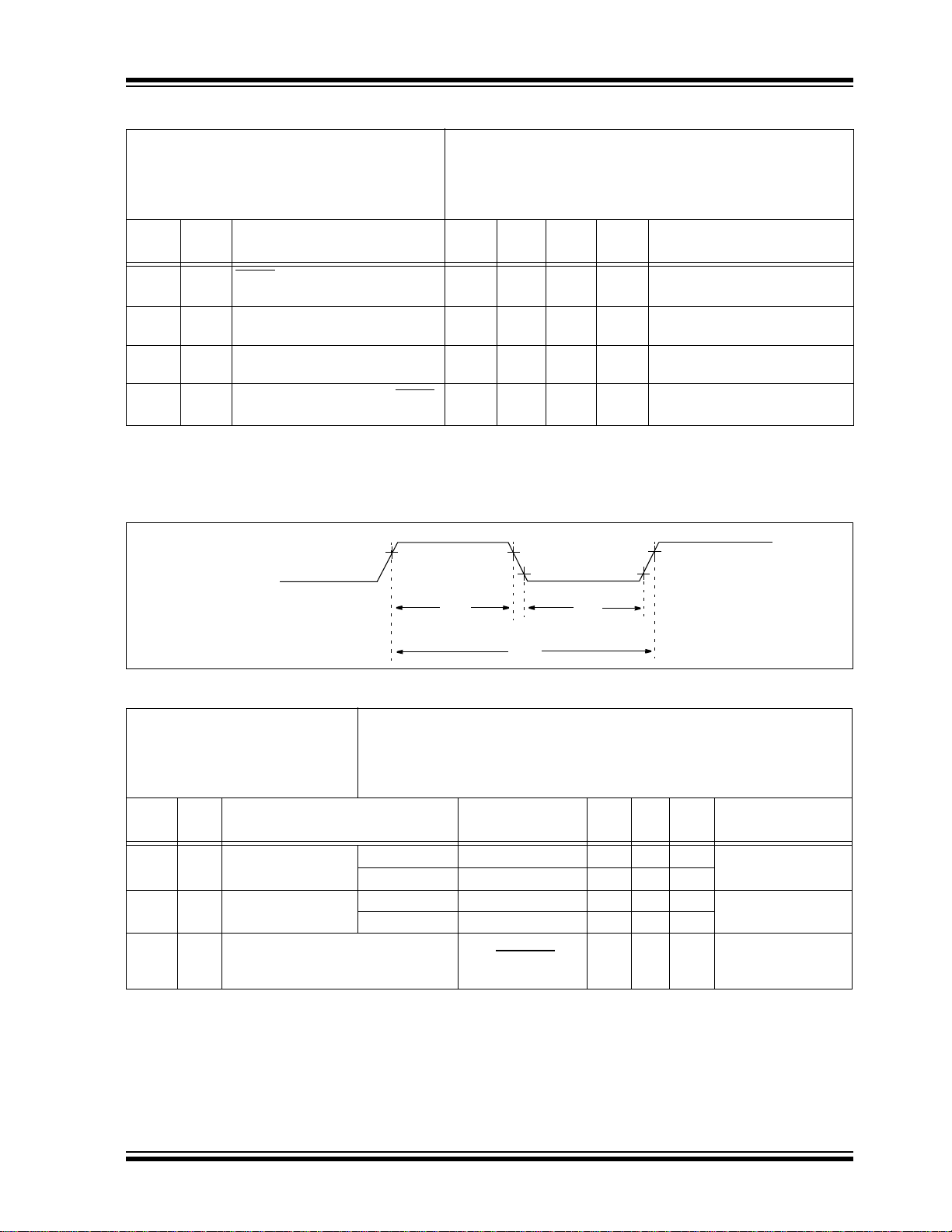
PIC10F200/202/204/206
TABLE 12-4: RESET, WATCHDOG TIMER AND DEVICE RESET TIMER – PIC10F200/202/204/206
Standard Operating Conditions (unless otherwise specified)
A ≤ +85°C (industrial)
A ≤ +125°C (extended)
AC CHARACTERISTICS
Param
No.
Sym Characteristic Min Typ
Operating Temperature -40°C ≤ T
-40°C ≤ T
Operating Voltage V
DD range is described in Section 12.1 “DC
Characteristics”
(1)
Max Units Conditions
30 T
31 TWDT Watchdog Timer Time-out Period
32 T
34 T
MC
MCLR Pulse Width (low) 2*
L
(no prescaler)
DRT Device Reset Timer Period (stan-
dard)
IOZ I/O High-impedance from MCLR
5*
10
10
10
10
—
—
16
16
16
16
—
—
29
31
29
31
μsμsVDD = 5V, -40°C to +85°C
msmsVDD = 5.0V (Industrial)
msmsVDD = 5.0V (Industrial)
——2*μs
V
DD = 5.0V
DD = 5.0V (Extended)
V
DD = 5.0V (Extended)
V
low
* These parameters are characterized but not tested.
Note 1: Data in the Typical (“Typ”) column is at 5V, 25°C unless otherwise stated. These parameters are for design
guidance only and are not tested.
FIGURE 12-4: TIMER0 CLOCK TIMINGS – PIC10F200/202/204/206
T0CKI
40 41
42
TABLE 12-5: TIMER0 CLOCK REQUIREMENTS – PIC10F200/202/204/206
Standard Operating Conditions (unless otherwise specified)
A ≤ +85°C (industrial)
A ≤ +125°C (extended)
(1)
AC CHARACTERISTICS
Param
Sym Characteristic Min Typ
No.
Operating Temperature -40°C ≤ T
-40°C ≤ T
Operating Voltage V
DD range is described in
Section 12.1 “DC Characteristics”.
Max Units Conditions
40 Tt0H T0CKI High Pulse
Width
41 Tt0L T0CKI Low Pulse
Width
42 Tt0P T0CKI Period T
No Prescaler 0.5 T
CY + 20* — — ns
With Prescaler 10* — — ns
No Prescaler 0.5 T
CY + 20* — — ns
With Prescaler 10* — — ns
CY + 40*
— — ns Whichever is greater.
20 or N
N = Prescale Value
(1, 2, 4,..., 256)
* These parameters are characterized but not tested.
Note 1: Data in the Typical (“Typ”) column is at 5V, 25°C unless otherwise stated. These parameters are for design
guidance only and are not tested.
© 2007 Microchip Technology Inc. DS41239D-page 71

PIC10F200/202/204/206
NOTES:
DS41239D-page 72 © 2007 Microchip Technology Inc.

PIC10F200/202/204/206
13.0 DC AND AC CHARACTERISTICS GRAPHS AND TABLES.
Note: The graphs and tables provided following this note are a statistical summary based on a limited number of
samples and are provided for informational purposes only. The performance characteristics listed herein are
not tested or guaranteed. In some graphs or tables, the data presented may be outside the specified
operating range (e.g., outside specified power supply range) and therefore, outside the warranted range.
“Typical” represents the mean of the distribution at 25°C. “Maximum” or “minimum” represents (mean + 3σ) or (mean -
3σ) respectively, where s is a standard deviation, over each temperature range.
FIGURE 13-1: IDD vs. VDD OVER FOSC
1,400
IDD (μA)
1,200
1,000
800
600
400
200
Typical: Statistical Mean @25°C
Maximum: Mean (Worst Case Temp) + 3σ
(-40°C to 125°C)
0
2.0 2.5 3.0 3.5 4.0 4.5 5.0 5.5
XT Mode
V
DD (V)
Maximum
4 MHz
Typical
4 MHz
© 2007 Microchip Technology Inc. DS41239D-page 73

PIC10F200/202/204/206
Typical
FIGURE 13-2: TYPICAL IPD vs. VDD (SLEEP MODE, ALL PERIPHERALS DISABLED)
(Sleep Mode all Peripherals Disabled)
0.45
Typical: Statistical Mean @25°C
Maximum: Mean (Worst Case Temp) + 3σ
(-40°C to 125°C)
2.0 2.5 3.0 3.5 4.0 4.5 5.0 5.5
DD (V)
V
IPD (μA)
0.40
0.35
0.30
0.25
0.20
0.15
0.10
0.05
0.0
FIGURE 13-3: MAXIMUM I
18.0
16.0
14.0
12.0
10.0
IPD (μA)
Typical: Statistical Mean @25°C
Maximum: Mean (Worst Case Temp) + 3σ
(-40°C to 125°C)
8.0
6.0
4.0
2.0
0.0
2.02.5 3.03.5 4.04.5 5.05.5
PD vs. VDD (SLEEP MODE, ALL PERIPHERALS DISABLED)
(Sleep Mode all Peripherals Disabled)
Maximum
Max. 125°C
Max. 85°C
V
DD (V)
DS41239D-page 74 © 2007 Microchip Technology Inc.

PIC10F200/202/204/206
FIGURE 13-4: COMPARATOR IPD vs. VDD (COMPARATOR ENABLED)
IPD (μA)
80
60
40
20
0
Typical: Statistical Mean @25°C
Maximum: Mean (Worst Case Temp) + 3σ
(-40°C to 125°C)
2.0 2.5 3.0 3.5 4.0 4.5 5.0 5.5
FIGURE 13-5: TYPICAL WDT I
9
8
7
Typical: Statistical Mean @25°C
Maximum: Mean (Worst Case Temp) + 3σ
(-40°C to 125°C)
PD vs. VDD
DD (V)
V
Maximum
Typical
IPD (μA)
6
5
4
3
2
1
0
2.0 2.5 3.0 3.5 4.0 4.5 5.0 5.5
DD (V)
V
© 2007 Microchip Technology Inc. DS41239D-page 75

PIC10F200/202/204/206
Maxi
FIGURE 13-6: MAXIMUM WDT IPD vs. VDD OVER TEMPERATURE
25.0
Typical: Statistical Mean @25°C
Maximum: Mean (Worst Case Temp) + 3σ
(-40°C to 125°C)
20.0
15.0
IPD (μA)
10.0
5.0
0.0
2.0 2.5 3.0 3.5 4.0 4.5 5.0 5.5
FIGURE 13-7: WDT TIME-OUT vs. V
DD OVER TEMPERATURE (NO PRESCALER)
mum
Max. 125°C
DD (V)
V
Max. 85°C
50
Typical: Statistical Mean @25°C
45
40
35
30
25
Time (ms)
20
15
10
5
0
2.0 2.5 3.0 3.5 4.0 4.5 5.0 5.5
Max. 125°C
Max. 85°C
Typical. 25°C
Min. -40°C
V
DD (V)
Maximum: Mean (Worst Case Temp) + 3σ
(-40°C to 125°C)
DS41239D-page 76 © 2007 Microchip Technology Inc.

PIC10F200/202/204/206
(VDD
125×C)
FIGURE 13-8: VOL vs. IOL OVER TEMPERATURE (VDD = 3.0V)
= 3V, -40×C TO
0.8
0.7
0.6
0.5
0.4
VOL (V)
0.3
0.2
0.1
0.0
Typical: Statistical Mean @25°C
Maximum: Mean (Worst Case Temp) + 3σ
(-40°C to 125°C)
Typical 25°C
Min. -40°C
5.0 5.5 6.0 6.5 7.0 7.5 8.0 8.5 9.0 9.5 10.0
I
OL (mA)
Max. 125°C
Max. 85°C
FIGURE 13-9: V
0.45
Typical: Statistical Mean @25°C
Maximum: Mean (Worst Case Temp) + 3σ
(-40°C to 125°C)
5.0 5.5 6.0 6.5 7.0 7.5 8.0 8.5 9.0 9.5 10.0
VOL (V)
0.40
0.35
0.30
0.25
0.20
0.15
0.10
0.05
0.00
OL vs. IOL OVER TEMPERATURE (VDD = 5.0V)
Typical: Statistical Mean @25×C
Maximum: Meas + 3 (-40×C to 125×C)
I
OL (mA)
Max. 125°C
Max. 85°C
Typ. 25°C
Min. -40°C
© 2007 Microchip Technology Inc. DS41239D-page 77
PIC10F200/202/204/206
(, )
FIGURE 13-10: VOH vs. IOH OVER TEMPERATURE (VDD = 3.0V)
3.5
3.0
2.5
2.0
VOH (V)
1.5
Typical: Statistical Mean @25°C
1.0
0.5
0.0
Maximum: Mean (Worst Case Temp) + 3σ
(-40°C to 125°C)
FIGURE 13-11: V
Max. -40°C
Typ. 25°C
Min. 125°C
-4.0-3.5-3.0-2.5-2.0-1.5-1.0-0.50.0
IOH (mA)
OH vs. IOH OVER TEMPERATURE (VDD = 5.0V)
5.5
5.0
Max. -40°C
4.5
VOH (V)
4.0
3.5
3.0
Typical: Statistical Mean @25°C
Maximum: Mean (Worst Case Temp) + 3σ
(-40°C to 125°C)
OH (mA)
I
Typ. 25°C
Min. 125°C
-5.0-4.5-4.0-3.5-3.0-2.5-2.0-1.5-1.0-0.50.0
DS41239D-page 78 © 2007 Microchip Technology Inc.

PIC10F200/202/204/206
(ST I
125×C)
FIGURE 13-12: TTL INPUT THRESHOLD VIN vs. VDD
(TTL Input, -40×C TO 125×C)
1.7
1.5
1.3
1.1
VIN (V)
0.9
0.7
0.5
Typical: Statistical Mean @25°C
Maximum: Mean (Worst Case Temp) + 3σ
(-40°C to 125°C)
Max. -40°C
Typ. 25°C
Min. 125°C
2.0 2.5 3.0 3.5 4.0 4.5 5.0 5.5
V
DD (V)
FIGURE 13-13: SCHMITT TRIGGER INPUT THRESHOLD VIN vs. VDD
nput, -40×C TO
4.0
3.5
3.0
2.5
Typical: Statistical Mean @25°C
Maximum: Mean (Worst Case Temp) + 3σ
(-40°C to 125°C)
VIH Max. 125°C
VIH Min. -40°C
VIN (V)
2.0
1.5
1.0
0.5
2.0 2.5 3.0 3.5 4.0 4.5 5.0 5.5
V
DD (V)
© 2007 Microchip Technology Inc. DS41239D-page 79
VIL Max. -40°C
VIL Min. 125°C

PIC10F200/202/204/206
FIGURE 13-14: INTOSC (INTERNAL OSCILLATOR) POWERUP TIMES vs. VDD
(Sleep Mode all Peripherals Disabled)
45
40
35
Maximum
30
25
20
Powerup Time (ms)
15
10
5
0
Max. 125°C
Max. 85°C
Typical 25°C
Max. -40°C
2.02.5 3.03.5 4.04.5 5.05.5
DD (V)
V
DS41239D-page 80 © 2007 Microchip Technology Inc.

14.0 PACKAGING INFORMATION
14.1 Package Marking Information
6-Lead SOT-23A*
PIC10F200/202/204/206
Example
XXNN
8-Lead PDIP
XXXXXXXX
XXXXXNNN
YYWW
8-Lead 2x3 DFN*
X X X
Y W W
N N
Legend: XX...X Customer-specific information
Y Year code (last digit of calendar year)
YY Year code (last 2 digits of calendar year)
WW Week code (week of January 1 is week ‘01’)
NNN Alphanumeric traceability code
3
e
Pb-free JEDEC designator for Matte Tin (Sn)
* This package is Pb-free. The Pb-free JEDEC designator ( )
can be found on the outer packaging for this package.
02JR
Example
PIC10F202
3
e
I/P 07Q
0520
Example
B E 0
6 1 0
1 7
3
e
Note: In the event the full Microchip part number cannot be marked on one line, it will
be carried over to the next line, thus limiting the number of available
characters for product-specific information.
© 2007 Microchip Technology Inc. DS41239D-page 81

PIC10F200/202/204/206
TABLE 14-1: 8-LEAD 2x3 DFN (MC) TOP
MARKING
Part Number Marking
PIC10F200-I/MC BA0
PIC10F200-E/MC BB0
PIC10F202-I/MC BC0
PIC10F202-E/MC BD0
PIC10F204-I/MC BE0
PIC10F204-E/MC BF0
PIC10F206-I/MC BG0
PIC10F206-E/MC BH0
TABLE 14-2: 6-LEAD SOT-23 (OT)
PACKAGE TOP MARKING
Part Number Marking
PIC10F200-I/OT 00NN
PIC10F200-E/OT 00NN
PIC10F202-I/OT 02NN
PIC10F202-E/OT 02NN
PIC10F204-I/OT 04NN
PIC10F204-E/OT 04NN
PIC10F206-I/OT 06NN
PIC10F206-E/OT 06NN
Note: NN represents the alphanumeric
traceability code.
DS41239D-page 82 © 2007 Microchip Technology Inc.
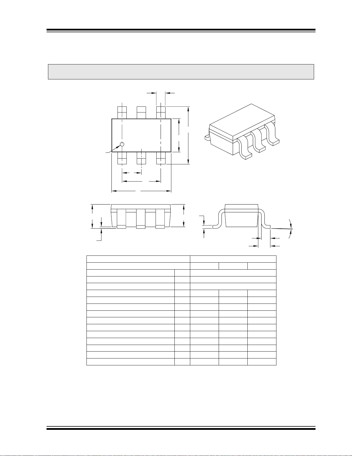
PIC10F200/202/204/206
6-Lead Plastic Small Outline Transistor (OT) [SOT-23]
B
Note: For the most current package drawings, please see the Microchip Packaging Specification located at
http://www.m icrochip.com/packaging
b
N
4
PIN 1 ID BY
LASER MARK
A
A1
Number of Pins N 6
Pitch e 0.95 BSC
Outside Lead Pitch e1 1.90 BSC
Overall Height A 0.90 – 1.45
Molded Package Thickness A2 0.89 – 1.30
Standoff A1 0.00 – 0.15
Overall Width E 2.20 – 3.20
Molded Package Width E1 1.30 – 1.80
Overall Length D 2.70 – 3.10
Foot Length L 0.10 – 0 .60
Footprint L1 0.35 – 0.80
Foot Angle φ 0° – 30°
Lead Thickness c 0.08 – 0.26
Lead Width b 0.20 – 0.51
Notes:
1. Dimensions D and E1 do not include mold flash or protrusions. Mold flash or protrusions shall not exceed 0.127 mm per side.
2. Dimensioning and tolerancing per ASME Y14.5M.
BSC: Basic Dimension. Theoretically exact value shown without tolerances.
1
2
e
3
e1
D
Dimension Limits MIN NOM MAX
E
E1
c
A2
Units MILLIMETERS
Microchip Technology Dra wing C04-0 28
φ
L
L1
© 2007 Microchip Technology Inc. DS41239D-page 83

PIC10F200/202/204/206
8-Lead Plastic Dual In-Line (P) – 300 mil Body [PDIP]
B
Note: For the most current package drawings, please see the Microchip Packaging Specification located at
http://www.m icrochip.com/packaging
N
Notes:
1. Pin 1 visual index feature may vary, but must be located with the hatched area.
2. § Significant Characteristic.
3. Dimensions D and E1 do not include mold flash or protrusions. Mold flash or protrusions shall not exceed .010" per side.
4. Dimensioning and tolerancing per ASME Y14.5M.
BSC: Basic Dimension. Theoretically exact value shown without tolerances.
NOTE 1
12
A
A1
b1
b
Number of Pins N 8
Pitch e .100 BSC
Top to Seating Plane A – – .210
Molded Package Thickness A2 .115 .130 .195
Base to Seating Plane A1 .015 – –
Shoulder to Shoulder Width E .290 .310 .325
Molded Package Width E1 .240 .250 .280
Overall Length D .348 .365 .400
Tip to Seating Plane L .115 .130 .150
Lead Thickness c .008 .010 .015
Upper Lead Width b1 .040 .060 .070
Lower Lead Width b .014 .018 .022
Overall Row Spacing § eB – – .430
3
D
e
Dimension Limits MIN NOM MAX
E1
E
A2
L
eB
Units I NCHES
c
Microchip Technology Dra wing C04-0 18
DS41239D-page 84 © 2007 Microchip Technology Inc.
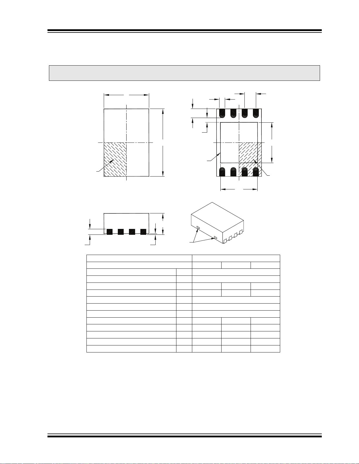
PIC10F200/202/204/206
8-Lead Plastic Dual Flat, No Lead Package (MC) – 2x3x0.9 mm Body [DFN]
B
Note: For the most current package drawings, please see the Microchip Packaging Specification located at
http://www.m icrochip.com/packaging
D
N
L
b
K
E
EXPOSED PAD
NOTE 1
2
1
TOP VIEW
A
A3 A1
Number of Pins N 8
Pitch e 0.50 BSC
Overall Height A 0.80 0.90 1.00
Standoff A1 0.00 0.02 0.05
Contact Thickness A3 0.20 REF
Overall Length D 2.00 BSC
Overall Width E 3.00 BSC
Exposed Pad Length D2 1.30 – 1.75
Exposed Pad Width E2 1.50 – 1.90
Contact Width b 0.18 0.25 0.30
Contact Length L 0.30 0.40 0.50
Contact-to-Exposed Pad K 0.20 – –
Notes:
1. Pin 1 visual index feature may vary, but must be located within the hatched area.
2. Package may have one or more exposed tie bars at ends.
3. Package is saw singulated.
4. Dimensioning and tolerancing per ASME Y14.5M.
BSC: Basic Dimension. Theoretically exact value shown without tolerances.
REF: Reference Dimens ion, usually without tolerance, for information purposes only.
NOTE 2
Units MILLIMETERS
Dimension Limits MIN NOM MAX
e
N
E2
1
2
D2
BOTTOM VIEW
Microchip Technology Drawing C04-123
NOTE 1
© 2007 Microchip Technology Inc. DS41239D-page 85

PIC10F200/202/204/206
NOTES:
DS41239D-page 86 © 2007 Microchip Technology Inc.

APPENDIX A: REVISION HISTORY
Revision C (August 2006)
Added 8-Pin DFN Pin Diagram; Revised Table 1-1;
Reformated all Registers; Revised Section 4.8 and
added note; Section 5.3 (changed Figure reference to
Figure 5-1); Tables 6-1 and 7-1 (removed shading from
TRISGPIO (I/O Control Register); Sections 8.1-8.4
(changed Table reference to Table 12-2); Section 14.1
Revised and replaced Package Marking Information
and drawings, Added Tables 14-1 & 14-2, Added DFN
Package drawing.
Revision D (April 2007)
Revised section 12.1, 12.2, 12.3, Table 1-1, 12-1, 12-3,
12-4. Added Section 13.0. Replaced Package Drawings (Rev. AP); Removed instances of PICmicro
replaced it with PIC
®
.
®
and
PIC10F200/202/204/206
© 2007 Microchip Technology Inc. DS41239D-page 87

PIC10F200/202/204/206
NOTES:
DS41239D-page 88 © 2007 Microchip Technology Inc.

INDEX
PIC10F200/202/204/206
A
Assembler
MPASM Assembler..................................................... 60
B
Block Diagram
On-Chip Reset Circuit................................................. 44
Timer0................................................................... 29, 33
TMR0/WDT Prescaler.....................................32, 36, 38
Watchdog Timer.......................................................... 47
Brown-Out Protection Circuit .............................................. 48
C
C Compilers
MPLAB C18 ................................................................ 60
MPLAB C30 ................................................................ 60
Carry .....................................................................................9
Clocking Scheme................................................................13
Code Protection ............................................................ 41, 50
Comparator
Comparator Module .................................................... 37
Configuration............................................................... 38
Interrupts..................................................................... 39
Operation .................................................................... 39
Reference ................................................................... 39
Configuration Bits ................................................................41
Customer Change Notification Service ............................... 91
Customer Notification Service............................................. 91
Customer Support ............................................................... 91
D
DC and AC Characteristics
Graphs and Tables ..................................................... 73
Development Support ......................................................... 59
Digit Carry............................................................................. 9
E
Errata ....................................................................................3
F
Family of Devices
PIC10F200/202/204/206...............................................5
G
GPIO ................................................................................... 25
I
I/O Interfacing ..................................................................... 25
I/O Ports.............................................................................. 25
I/O Programming Considerations........................................26
ID Locations.................................................................. 41, 50
INDF.................................................................................... 23
Indirect Data Addressing..................................................... 23
Instruction Cycle ................................................................. 13
Instruction Flow/Pipelining ..................................................13
Instruction Set Summary..................................................... 52
Internet Address.................................................................. 91
L
Loading of PC .....................................................................22
M
Memory Organization.......................................................... 15
Data Memory .............................................................. 16
Program Memory (PIC10F200/204) ........................... 15
Program Memory (PIC10F202/206) ........................... 16
Microchip Internet Web Site................................................ 91
MPLAB ASM30 Assembler, Linker, Librarian ..................... 60
MPLAB ICD 2 In-Circuit Debugger ..................................... 61
MPLAB ICE 2000 High-Performance Universal
In-Circuit Emulator...................................................... 61
MPLAB ICE 4000 High-Performance Universal
In-Circuit Emulator...................................................... 61
MPLAB Integrated Development Environment Software.... 59
MPLAB PM3 Device Programmer ...................................... 61
MPLINK Object Linker/MPLIB Object Librarian .................. 60
O
Option Register................................................................... 20
OSCCAL Register............................................................... 21
Oscillator Configurations..................................................... 42
Oscillator Types
HS............................................................................... 42
LP ............................................................................... 42
P
PIC10F200/202/204/206 Device Varieties............................ 7
PICSTART Plus Development Programmer....................... 62
POR
Device Reset Timer (DRT) ................................... 41, 46
............................................................................... 48
PD
Power-on Reset (POR)............................................... 41
TO
............................................................................... 48
Power-down Mode.............................................................. 49
Prescaler ...................................................................... 31, 35
Program Counter ................................................................ 22
Q
Q cycles.............................................................................. 13
R
Reader Response............................................................... 92
Read-Modify-Write.............................................................. 26
Register File Map
PIC10F200/204 .......................................................... 17
PIC10F202/206 .......................................................... 17
Registers
Special Function ......................................................... 18
Reset .................................................................................. 41
Reset on Brown-Out........................................................... 48
S
Sleep ............................................................................ 41, 49
Software Simulator (MPLAB SIM) ...................................... 60
Special Features of the CPU.............................................. 41
Special Function Registers................................................. 18
Stack................................................................................... 22
Status Register............................................................... 9, 19
T
Timer0
Timer0 .................................................................. 29, 33
Timer0 (TMR0) Module ........................................ 29, 33
TMR0 with External Clock .................................... 30, 34
Timing Parameter Symbology and Load Conditions .......... 69
TRIS Registers ................................................................... 25
© 2007 Microchip Technology Inc. DS41239D-page 89

PIC10F200/202/204/206
W
Wake-up from Sleep ........................................................... 49
Watchdog Timer (WDT) ................................................ 41, 46
Period..........................................................................46
Programming Considerations ..................................... 46
WWW Address.................................................................... 91
WWW, On-Line Support........................................................ 3
Z
Zero bit..................................................................................9
DS41239D-page 90 © 2007 Microchip Technology Inc.

PIC10F200/202/204/206
THE MICROCHIP WEB SITE
Microchip provides online support via our WWW site at
www.microchip.com. This web site is used as a means
to make files and information easily available to
customers. Accessible by using your favorite Internet
browser, the web site contains the following
information:
• Product Support – Data sheets and errata,
application notes and sample programs, design
resources, user’s guides and hardware support
documents, latest software releases and archived
software
• General Technical Support – Frequently Asked
Questions (FAQ), technical support requests,
online discussion groups, Microchip consultant
program member listing
• Business of Microchip – Product selector and
ordering guides, latest Microchip press releases,
listing of seminars and events, listings of
Microchip sales offices, distributors and factory
representatives
CUSTOMER CHANGE NOTIFICATION
SERVICE
CUSTOMER SUPPORT
Users of Microchip products can receive assistance
through several channels:
• Distributor or Representative
• Local Sales Office
• Field Application Engineer (FAE)
• Technical Support
• Development Systems Information Line
Customers should contact their distributor,
representative or field application engineer (FAE) for
support. Local sales offices are also available to help
customers. A listing of sales offices and locations is
included in the back of this document.
Technical support is available through the web site
at: http://support.microchip.com
Microchip’s customer notification service helps keep
customers current on Microchip products. Subscribers
will receive e-mail notification whenever there are
changes, updates, revisions or errata related to a
specified product family or development tool of interest.
To register, access the Microchip web site at
www.microchip.com, click on Customer Change
Notification and follow the registration instructions.
© 2007 Microchip Technology Inc. DS41239D-page 91

PIC10F200/202/204/206
READER RESPONSE
It is our intention to provide you with the best documentation possible to ensure successful use of your Microchip product. If you wish to provide your comments on organization, clarity, subject matter, and ways in which our documentation
can better serve you, please FAX your comments to the Technical Publications Manager at (480) 792-4150.
Please list the following information, and use this outline to provide us with your comments about this document.
To :
RE: Reader Response
From:
Application (optional):
Would you like a reply? Y N
Device: Literature Number:
Questions:
1. What are the best features of this document?
2. How does this document meet your hardware and software development needs?
3. Do you find the organization of this document easy to follow? If not, why?
Technical Publications Manager
Name
Company
Address
City / State / ZIP / Country
Telephone: (_______) _________ - _________
Total Pages Sent ________
FAX: (______) _________ - _________
DS41239DPIC10F200/202/204/206
4. What additions to the document do you think would enhance the structure and subject?
5. What deletions from the document could be made without affecting the overall usefulness?
6. Is there any incorrect or misleading information (what and where)?
7. How would you improve this document?
DS41239D-page 92 © 2007 Microchip Technology Inc.

PIC10F200/202/204/206
PRODUCT IDENTIFICATION SYSTEM
To order or obtain information, e.g., on pricing or delivery, refer to the factory or the listed sales office.
PART NO. X /XX XXX
Device
Range
Device: PIC10F200
PIC10F202
PIC10F204
PIC10F206
PIC10F200T (Tape & Reel)
PIC10F202T (Tape & Reel)
PIC10F204T (Tape & Reel)
PIC10F206T (Tape & Reel)
PatternPackageTemperature
Examples:
a) PIC10F200-I/P = Industrial temp., PDIP
package (Pb-free)
b) PIC10F202T-E/OT = Extended temp., SOT-23
package (Pb-free), Tape and Reel
c) PIC10F202-E/MC = Extended temp., DFN-
package (Pb-free)
Temperature
Range:
Package: P = 300 mil PDIP (Pb-free)
Pattern: Special Requirements
I= -40°C to +85°C (Industrial)
E= -40°C to +125°C (Extended)
OT = SOT-23, 6-LD (Pb-free)
MC = DFN, 8-LD 2x3 (Pb-free)
© 2007 Microchip Technology Inc. DS41239D-page 93

WORLDWIDE SALES AND SERVICE
AMERICAS
Corporate Office
2355 West Chandler Blvd.
Chandler, AZ 85224-6199
Tel: 480-792-7200
Fax: 480-792-7277
Technical Support:
http://support.microchip.com
Web Address:
www.microchip.com
Atlanta
Duluth, GA
Tel: 678-957-9614
Fax: 678-957-1455
Boston
Westborough, MA
Tel: 774-760-0087
Fax: 774-760-0088
Chicago
Itasca, IL
Tel: 630-285-0071
Fax: 630-285-0075
Dallas
Addison, TX
Tel: 972-818-7423
Fax: 972-818-2924
Detroit
Farmington Hills, MI
Tel: 248-538-2250
Fax: 248-538-2260
Kokomo
Kokomo, IN
Tel: 765-864-8360
Fax: 765-864-8387
Los Angeles
Mission Viejo, CA
Tel: 949-462-9523
Fax: 949-462-9608
Santa Clara
Santa Clara, CA
Tel: 408-961-6444
Fax: 408-961-6445
Toronto
Mississauga, Ontario,
Canada
Tel: 905-673-0699
Fax: 905-673-6509
ASIA/PACIFIC
Asia Pacific Office
Suites 3707-14, 37th Floor
Tower 6, The Gateway
Habour City, Kowloon
Hong Kong
Tel: 852-2401-1200
Fax: 852-2401-3431
Australia - Sydney
Tel: 61-2-9868-6733
Fax: 61-2-9868-6755
China - Beijing
Tel: 86-10-8528-2100
Fax: 86-10-8528-2104
China - Chengdu
Tel: 86-28-8665-5511
Fax: 86-28-8665-7889
China - Fuzhou
Tel: 86-591-8750-3506
Fax: 86-591-8750-3521
China - Hong Kong SAR
Tel: 852-2401-1200
Fax: 852-2401-3431
China - Qingdao
Tel: 86-532-8502-7355
Fax: 86-532-8502-7205
China - Shanghai
Tel: 86-21-5407-5533
Fax: 86-21-5407-5066
China - Shenyang
Tel: 86-24-2334-2829
Fax: 86-24-2334-2393
China - Shenzhen
Tel: 86-755-8203-2660
Fax: 86-755-8203-1760
China - Shunde
Tel: 86-757-2839-5507
Fax: 86-757-2839-5571
China - Wuhan
Tel: 86-27-5980-5300
Fax: 86-27-5980-5118
China - Xian
Tel: 86-29-8833-7250
Fax: 86-29-8833-7256
ASIA/PACIFIC
India - Bangalore
Tel: 91-80-4182-8400
Fax: 91-80-4182-8422
India - New Delhi
Tel: 91-11-4160-8631
Fax: 91-11-4160-8632
India - Pune
Tel: 91-20-2566-1512
Fax: 91-20-2566-1513
Japan - Yokohama
Tel: 81-45-471- 6166
Fax: 81-45-471-6122
Korea - Gumi
Tel: 82-54-473-4301
Fax: 82-54-473-4302
Korea - Seoul
Tel: 82-2-554-7200
Fax: 82-2-558-5932 or
82-2-558-5934
Malaysia - Penang
Tel: 60-4-646-8870
Fax: 60-4-646-5086
Philippines - Manila
Tel: 63-2-634-9065
Fax: 63-2-634-9069
Singapore
Tel: 65-6334-8870
Fax: 65-6334-8850
Taiwan - Hsin Chu
Tel: 886-3-572-9526
Fax: 886-3-572-6459
Taiwan - Kaohsiung
Tel: 886-7-536-4818
Fax: 886-7-536-4803
Taiwan - Taipei
Tel: 886-2-2500-6610
Fax: 886-2-2508-0102
Thailand - Bangkok
Tel: 66-2-694-1351
Fax: 66-2-694-1350
EUROPE
Austria - Wels
Tel: 43-7242-2244-39
Fax: 43-7242-2244-393
Denmark - Copenhagen
Tel: 45-4450-2828
Fax: 45-4485-2829
France - Paris
Tel: 33-1-69-53-63-20
Fax: 33-1-69-30-90-79
Germany - Munich
Tel: 49-89-627-144-0
Fax: 49-89-627-144-44
Italy - Milan
Tel: 39-0331-742611
Fax: 39-0331-466781
Netherlands - Drunen
Tel: 31-416-690399
Fax: 31-416-690340
Spain - Madrid
Tel: 34-91-708-08-90
Fax: 34-91-708-08-91
UK - Wokingham
Tel: 44-118-921-5869
Fax: 44-118-921-5820
12/08/06
DS41239D-page 94 © 2007 Microchip Technology Inc.
 Loading...