

Page 1

MIC33M656
Evaluation Board
User’s Guide
2019 Microchip Technology Inc. DS50002914A
Page 2

Note the following details of the code protection feature on Microchip devices:
• Microchip products meet the specification contained in their particular Microchip Data Sheet.
• Microchip believes that its family of products is one of the most secure families of its kind on the market today, when used in the
intended manner and under normal conditions.
• There are dishonest and possibly illegal methods used to breach the code protection feature. All of these methods, to our
knowledge, require using the Microchip products in a manner outside the operating specifications contained in Microchip’s Data
Sheets. Most likely, the person doing so is engaged in theft of intellectual property.
• Microchip is willing to work with the customer who is concerned about the integrity of their code.
• Neither Microchip nor any other semiconductor manufacturer can guarantee the security of their code. Code protection does not
mean that we are guaranteeing the product as “unbreakable.”
Code protection is constantly evolving. We at Microchip are committed to continuously improving the code protection features of our
products. Attempts to break Microchip’s code protection feature may be a violation of the Digital Millennium Copyright Act. If such acts
allow unauthorized access to your software or other copyrighted work, you may have a right to sue for relief under that Act.
Information contained in this publication regarding device
applications and the like is provided only for your convenience
and may be superseded by updates. It is your responsibility to
ensure that your application meets with your specifications.
MICROCHIP MAKES NO REPRESENTATIONS OR
WARRANTIES OF ANY KIND WHETHER EXPRESS OR
IMPLIED, WRITTEN OR ORAL, STATUTORY OR
OTHERWISE, RELATED TO THE INFORMATION,
INCLUDING BUT NOT LIMITED TO ITS CONDITION,
QUALITY, PERFORMANCE, MERCHANTABILITY OR
FITNESS FOR PURPOSE. Microchip disclaims all liability
arising from this information and its use. Use of Microchip
devices in life support and/or safety applications is entirely at
the buyer’s risk, and the buyer agrees to defend, indemnify and
hold harmless Microchip from any and all damages, claims,
suits, or expenses resulting from such use. No licenses are
conveyed, implicitly or otherwise, under any Microchip
intellectual property rights unless otherwise stated.
Trademarks
The Microchip name and logo, the Microchip logo, Adaptec,
AnyRate, AVR, AVR logo, AVR Freaks, BesTime, BitCloud, chipKIT,
chipKIT logo, CryptoMemory, CryptoRF, dsPIC, FlashFlex,
flexPWR, HELDO, IGLOO, JukeBlox, KeeLoq, Kleer, LANCheck,
LinkMD, maXStylus, maXTouch, MediaLB, megaAVR, Microsemi,
Microsemi logo, MOST, MOST logo, MPLAB, OptoLyzer,
PackeTime, PIC, picoPower, PICSTART, PIC32 logo, PolarFire,
Prochip Designer, QTouch, SAM-BA, SenGenuity, SpyNIC, SST,
SST Logo, SuperFlash, Symmetricom, SyncServer, Tachyon,
TempTrackr, TimeSource, tinyAVR, UNI/O, Vectron, and XMEGA
are registered trademarks of Microchip Technology Incorporated in
the U.S.A. and other countries.
APT, ClockWorks, The Embedded Control Solutions Company,
EtherSynch, FlashTec, Hyper Speed Control, HyperLight Load,
IntelliMOS, Libero, motorBench, mTouch, Powermite 3, Precision
Edge, ProASIC, ProASIC Plus, ProASIC Plus logo, Quiet-Wire,
SmartFusion, SyncWorld, Temux, TimeCesium, TimeHub,
TimePictra, TimeProvider, Vite, WinPath, and ZL are registered
trademarks of Microchip Technology Incorporated in the U.S.A.
Adjacent Key Suppression, AKS, Analog-for-the-Digital Age, Any
Capacitor, AnyIn, AnyOut, BlueSky, BodyCom, CodeGuard,
CryptoAuthentication, CryptoAutomotive, CryptoCompanion,
CryptoController, dsPICDEM, dsPICDEM.net, Dynamic Average
Matching, DAM, ECAN, EtherGREEN, In-Circuit Serial
Programming, ICSP, INICnet, Inter-Chip Connectivity, JitterBlocker,
KleerNet, KleerNet logo, memBrain, Mindi, MiWi, MPASM, MPF,
MPLAB Certified logo, MPLIB, MPLINK, MultiTRAK, NetDetach,
Omniscient Code Generation, PICDEM, PICDEM.net, PICkit,
PICtail, PowerSmart, PureSilicon, QMatrix, REAL ICE, Ripple
Blocker, SAM-ICE, Serial Quad I/O, SMART-I.S., SQI,
SuperSwitcher, SuperSwitcher II, Total Endurance, TSHARC,
USBCheck, VariSense, ViewSpan, WiperLock, Wireless DNA, and
ZENA are trademarks of Microchip Technology Incorporated in the
U.S.A. and other countries.
SQTP is a service mark of Microchip Technology Incorporated in
the U.S.A.
The Adaptec logo, Frequency on Demand, Silicon Storage
Technology, and Symmcom are registered trademarks of Microchip
Technology Inc. in other countries.
GestIC is a registered trademark of Microchip Technology Germany
II GmbH & Co. KG, a subsidiary of Microchip Technology Inc., in
other countries.
All other trademarks mentioned herein are property of their
respective companies.
© 2019, Microchip Technology Incorporated, All Rights Reserved.
For information regarding Microchip’s Quality Management Systems,
please visit www.microchip.com/quality.
ISBN: 978-1-5224-5089-4
DS50002914A-page 2 2019 Microchip Technology Inc.
Page 3

MIC33M656
EVALUATION BOARD
USER’S GUIDE
Table of Contents
Preface ........................................................................................................................... 5
Introduction............................................................................................................ 5
Document Layout .................................................................................................. 5
Conventions Used in this Guide ............................................................................ 6
Recommended Reading........................................................................................ 7
The Microchip Website .......................................................................................... 7
Product Change Notification Service..................................................................... 7
Customer Support ................................................................................................. 7
Document Revision History ................................................................................... 7
Chapter 1. Product Overview........................................................................................ 9
1.1 Introduction ..................................................................................................... 9
1.2 MIC33M656 Short Overview .......................................................................... 9
1.3 What is the MIC33M656 Evaluation Board? ................................................ 10
1.4 Contents of the MIC33M656 Evaluation Board Kit ....................................... 10
Chapter 2. Installation and Operation ........................................................................ 11
2.1 Introduction ................................................................................................... 11
2.2 Features ....................................................................................................... 12
2.3 Getting Started ............................................................................................. 12
Chapter 3. GUI Installation and Operation................................................................. 17
3.1 Getting Started ............................................................................................. 17
3.2 Graphical User Interface Installation ............................................................ 17
2
3.3 I
C Monitor Graphical User Interface Uninstall ............................................ 20
Chapter 4. GUI Description ......................................................................................... 21
4.1 Introduction ................................................................................................... 21
4.2 The Graphical User Interface ....................................................................... 22
Appendix A. Schematic and Layouts......................................................................... 29
A.1 Introduction .................................................................................................. 29
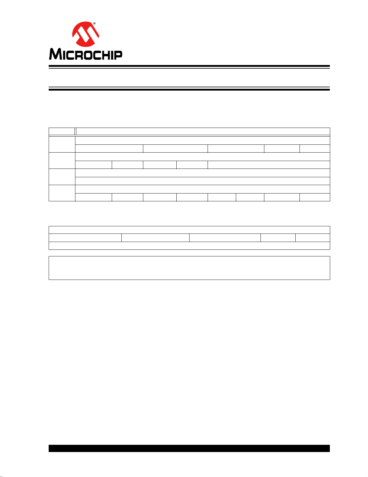
A.2 Board – Schematic ....................................................................................... 30
A.3 Board – Top Silk .......................................................................................... 31
A.4 Board – Top Copper and Silk ....................................................................... 31
A.5 Board – Top Copper .................................................................................... 32
A.6 Board – Signal Layer 1 ................................................................................ 32
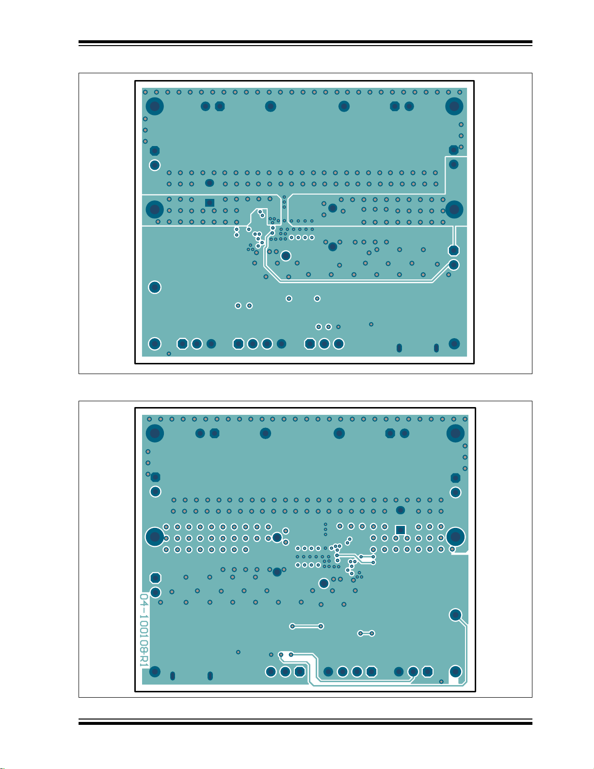
A.7 Board – Signal Layer 2 ................................................................................ 33
A.8 Board – Bottom Copper ............................................................................... 33
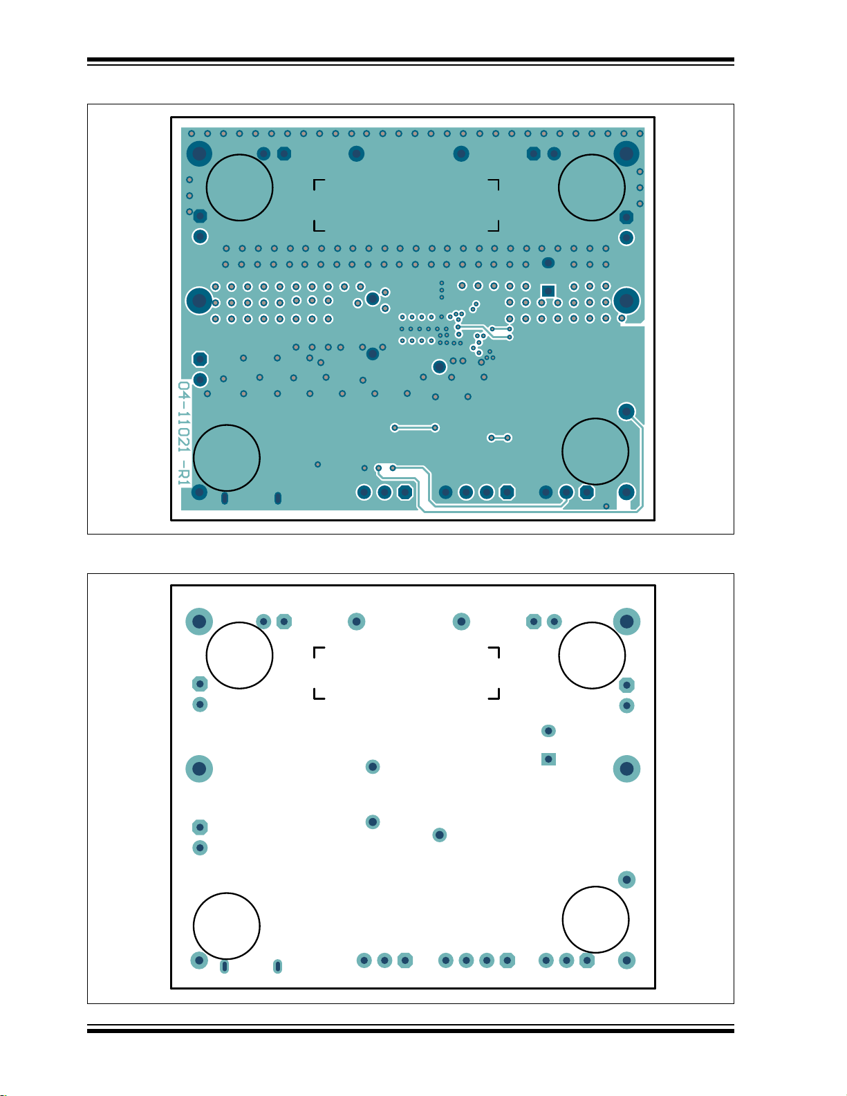
A.9 Board – Bottom Copper and Silk ................................................................. 34
A.10 Board – Bottom Silk ................................................................................... 34
2019 Microchip Technology Inc. DS50002914A-page 3
Page 4

MIC33M656 Evaluation Board User’s Guide
Appendix B. Bill of Materials (BOM) ...........................................................................35
Appendix C. MIC33M656 Internal Registers...............................................................37
C.1 Register Map and I2C Programmability ....................................................... 37
Worldwide Sales and Service .....................................................................................42
DS50002914A-page 4 2019 Microchip Technology Inc.
Page 5

MIC33M656
EVALUATION BOARD
USER’S GUIDE
Preface
NOTICE TO CUSTOMERS
All documentation becomes dated, and this manual is no exception. Microchip tools and
documentation are constantly evolving to meet customer needs, so some actual dialogs
and/or tool descriptions may differ from those in this document. Please refer to our website
(www.microchip.com) to obtain the latest documentation available.
Documents are identified with a “DS” number. This number is located on the bottom of each
page, in front of the page number. The numbering convention for the DS number is
“DSXXXXXXXXA”, where “XXXXXXXX” is the document number and “A” is the revision level
of the document.
For the most up-to-date information on development tools, see the MPLAB
Select the Help menu, and then Topics, to open a list of available online help files.
®
IDE online help.
INTRODUCTION
This chapter contains general information that will be useful to know before using the
MIC33M656 Evaluation Board. Items discussed in this chapter include:
• Document Layout
• Conventions Used in this Guide
• Recommended Reading
• The Microchip Website
• Product Change Notification Service
• Customer Support
• Document Revision History
DOCUMENT LAYOUT
This document describes how to use the MIC33M656 Evaluation Board as a
development tool. The manual layout is as follows:
• Chapter 1. “Product Overview” – Important information about the MIC33M656
device.
• Chapter 2. “Installation and Operation” – Includes instructions on how to get
started with the MIC33M656 Evaluation Board and a description of each function.
• Chapter 3. “GUI Installation and Operation” – Includes instructions on how to
install the Graphical User Interface (GUI).
• Chapter 4. “GUI Description” – Describes the items included in the Graphical
User Interface.
• Appendix A. “Schematic and Layouts” – Shows the schematic and PCB layout
diagrams for the MIC33M656 Evaluation Board.
• Appendix B. “Bill of Materials (BOM)” – Lists the parts used to build the
MIC33M656 Evaluation Board.
• Appendix C. “MIC33M656 Internal Registers” – Describes the MIC33M656
device’s internal registers.
2019 Microchip Technology Inc. DS50002914A-page 5
Page 6

MIC33M656 Evaluation Board User’s Guide
CONVENTIONS USED IN THIS GUIDE
This manual uses the following documentation conventions:
DOCUMENTATION CONVENTIONS
Description Represents Examples
Arial font:
Italic characters Referenced books MPLAB® IDE User’s Guide
Emphasized text ...is the only compiler...
Initial caps A window the Output window
A dialog the Settings dialog
A menu selection select Enable Programmer
Quotes A field name in a window or
dialog
Underlined, italic text with
right angle bracket
Bold characters A dialog button Click OK
N‘Rnnnn A number in verilog format,
Text in angle brackets < > A key on the keyboard Press <Enter>, <F1>
Courier New font:
Plain Courier New Sample source code #define START
Italic Courier New A variable argument file.o, where file can be
Square brackets [ ] Optional arguments mcc18 [options] file
Curly brackets and pipe
character: { | }
Ellipses... Replaces repeated text var_name [,
A menu path File>Save
A tab Click the Power tab
where N is the total number of
digits, R is the radix and n is a
digit.
Filenames autoexec.bat
File paths c:\mcc18\h
Keywords _asm, _endasm, static
Command-line options -Opa+, -Opa-
Bit values 0, 1
Constants 0xFF, ‘A’
Choice of mutually exclusive
arguments; an OR selection
Represents code supplied by
user
“Save project before build”
4‘b0010, 2‘hF1
any valid filename
[options]
errorlevel {0|1}
var_name...]
void main (void)
{ ...
}
DS50002914A-page 6 2019 Microchip Technology Inc.
Page 7

RECOMMENDED READING
This user’s guide describes how to use the MIC33M656 Evaluation Board. Other
useful documents are listed below. The following Microchip document is available and
recommended as a supplemental reference resource:
• MIC33M656 Data Sheet – “6A, Power Module Buck Converter with
HyperLight Load
THE MICROCHIP WEBSITE
Microchip provides online support via our website at www.microchip.com. This website
is used as a means to make files and information easily available to customers.
Accessible by using your favorite Internet browser, the website contains the following
information:
• Product Support – Data sheets and errata, application notes and sample
programs, design resources, user’s guides and hardware support documents,
latest software releases and archived software
• General Technical Support – Frequently Asked Questions (FAQs), technical
support requests, online discussion groups, Microchip consultant program
member listing
• Business of Microchip – Product selector and ordering guides, latest Microchip
press releases, listing of seminars and events, listings of Microchip sales offices,
distributors and factory representatives
®
and I2C Interface” (DS20006256)
Preface
PRODUCT CHANGE NOTIFICATION SERVICE
Microchip’s customer notification service helps keep customers current on Microchip
products. Subscribers will receive e-mail notifications whenever there are changes,
updates, revisions or errata related to a specified product family or development tool of
interest.
To register, access the Microchip website at www.microchip.com, click on Product
Change Notification and follow the registration instructions.
CUSTOMER SUPPORT
Users of Microchip products can receive assistance through several channels:
• Distributor or Representative
• Local Sales Office
• Field Application Engineer (FAE)
• Technical Support
Customers should contact their distributor, representative or field application engineer
(FAE) for support. Local sales offices are also available to help customers. A listing of
sales offices and locations is included in the back of this document.
Technical support is available through the website at:
http://www.microchip.com/support.
DOCUMENT REVISION HISTORY
Revision A (September 2019)
• Initial Release of this Document.
2019 Microchip Technology Inc. DS50002914A-page 7
Page 8

MIC33M656 Evaluation Board User’s Guide
NOTES:
DS50002914A-page 8 2019 Microchip Technology Inc.
Page 9

Chapter 1. Product Overview
C3
47 µF
C4
47 µF
V
OUT
Enable
V
IN
2.4V to 5.5V
C
10 µF
1.0V/6A
V
IN
SCL
SDA
PG
SW
MIC33M656
OUT
V
OUT
PGND
AGND
PG
SCL
SDA
EN
PV
IN
AUX_PV
IN
SV
IN
SW
AUX_GND
1.1 INTRODUCTION
This chapter provides an overview of the MIC33M656 Evaluation Board and covers the
following topics:
• MIC33M656 Short Overview
• What is the MIC33M656 Evaluation Board?
• Contents of the MIC33M656 Evaluation Board Kit
1.2 MIC33M656 SHORT OVERVIEW
The MIC33M656 is an I2C programmable, high-efficiency, low-voltage input,
6A current, synchronous step-down regulator power module with integrated inductor.
The Constant-On-Time (COT) control architecture with HyperLight Load
vides very high efficiency at light loads, while still having ultra-fast transient response.
The user can program, via the I
voltage, on-time, soft start slope, high-side current limit, HLL or Forced PWM mode of
operation. The 2.4V to 5.5V input voltage range, low shutdown and quiescent currents
make the MIC33M656 ideal for single-cell Li-Ion, battery-powered applications.
An open-drain Power Good (PG) output is provided to indicate when the output voltage
is within 9% of regulation, and facilitates output voltage monitoring and sequencing.
When set in Shutdown mode (EN = GND), the current consumption of MIC33M656 is
reduced to 1.5 µA (typical).
The MIC33M656 is available in a thermally efficient, 53-Lead, 6 mm x 10 mm x 3 mm
QFN package, with an operating junction temperature range from -40°C to +125°C.
More detailed information regarding the capabilities of the MIC33M656 are available in
the “MIC33M656 Data Sheet”.
MIC33M656
EVALUATION BOARD
USER’S GUIDE
®
(HLL) pro-
2
C interface, various parameters, such as output
FIGURE 1-1: Typical MIC33M656 Step-Down Application.
2019 Microchip Technology Inc. DS50002914A-page 9
Page 10

MIC33M656 Evaluation Board User’s Guide
1.3 WHAT IS THE MIC33M656 EVALUATION BOARD?
The MIC33M656 Evaluation Board is used to evaluate and demonstrate Microchip
Technology’s MIC33M656 device. This Evaluation Board demonstrates the
MIC33M656 in a buck converter application, supplied from an external voltage source
(2.4V-5.5V), with an I
comprehensive control and status reporting with the MIC33M656.
1.4 CONTENTS OF THE MIC33M656 EVALUATION BOARD KIT
The MIC33M656 Evaluation Board kit includes:
• MIC33M656 Evaluation Board (DT100108)
• Important Information Sheet
2
C programmed regulated output. The I2C monitor GUI allows
DS50002914A-page 10 2019 Microchip Technology Inc.
Page 11

Chapter 2. Installation and Operation
MCP2221
MIC33M656
USB
I/F
V
USB
Data
PWR
V
IN
V
OUT
PWR
SCL
SDA
V
IN
PG
EN
SCL
SDA
PG
EN
Note 2
Note 1
Note 1: Three-way jumper fitted for selection of I2C pull-up voltage.
2: I
2
C bus (SDA, SCL), EN control and PG status via MCP2221 USB bridge.
2.1 INTRODUCTION
The MIC33M656 Evaluation Board has been developed to test the MIC33M656 module
capabilities, including loading up to 6A, control and monitor through the USB interface
(via the I
communication.
MIC33M656
EVALUATION BOARD
USER’S GUIDE
2
C monitor GUI). Pin headers are also fitted for Bode analysis and external I2C
FIGURE 2-1: MIC33M656 Step-Down Regulator with MCP2221 I
2
C Bridge.
2019 Microchip Technology Inc. DS50002914A-page 11
Page 12

MIC33M656 Evaluation Board User’s Guide
2.2 FEATURES
The MIC33M656 Evaluation Board has the following features:
• Input Voltage Range: 2.4V to 5.5V
• 6A (maximum) Continuous Output Current
• Multiple Faults Indication through I
2
C Programmable:
•I
- Output voltage: 0.6-1.28V, 5 mV resolution
- Slew rate: 0.2-3.2 ms/V
- Switching frequency: up to 2.5 MHz
- High-side current limit: 3.5-10A
- Enable delay: 0.25-3 ms
- Output discharge when disabled
• High Efficiency (up to 95%)
• ±1.5% Output Voltage Accuracy Over Line/Load/Temperature Range
• Safe Start-up with Pre-Biased Output
• Typical 1.5 µA Shutdown Supply Current
• Low Dropout (100% Duty Cycle) Operation
• Ultra-Fast Transient Response
• Latch-Off Thermal Shutdown Protection
• Latch-Off Current Limit Protection
• Power Good Open-Drain Output
2
C
2.3 GETTING STARTED
The MIC33M656 Evaluation Board is fully assembled and tested to evaluate and
demonstrate the MIC33M656 module. This Evaluation Board requires the use of external lab supplies and a PC. The MIC33M656 is offered in four different product options,
depending on the default settings at power-up, prior to any I
differences among the various product options are described in the “MIC33M656 Data
Sheet”. The Evaluation Board carries the HAYMP option, whose default output voltage
is 1.0V. All of the device options may be fitted on the board, as is.
2
C write operation. The
DS50002914A-page 12 2019 Microchip Technology Inc.
Page 13

Installation and Operation
2.3.1 Power Input and Output Connection
2.3.1.1 POWERING THE MIC33M656 EVALUATION BOARD
When the Evaluation Board is ready for evaluation, apply positive input voltage to the
V
terminal and the corresponding return to the GND_IN terminal. The maximum input
IN
voltage should not exceed 5.5V. An electronic load or resistive load can be used for
evaluation. Some electronic loads can sink the programmed current, starting from very
low output voltage levels during start-up. For a more realistic start-up behavior evaluation, a resistive load or Constant Resistance mode for electronic load is recommended.
Connect the positive voltage terminal of the load to the V
Board and connect the negative or return side of the load to the GND_OUT terminal. If
changing the regulator parameters is required, or simply to monitor the part, make sure
to connect the Micro-USB cable between the Evaluation Board and the PC. Then,
install the GUI according to Chapter 3. “GUI Installation and Operation” and follow
the indications in Chapter 2. “Installation and Operation” for more extensive
evaluation.
Note: The inductance associated with long wires on the board input may cause
voltage spikes at load stepping or start-up into a heavy load. If the spikes
exceed the 5.5V maximum input voltage rating, the MIC33M656 may fail.
This can be prevented by populating a 470
C8 footprint.
terminal on the Evaluation
OUT
µF electrolytic capacitor on the
2.3.1.2 EVALUATION BOARD POWER-UP PROCEDURE
For the power-up procedure, follow the steps bellow:
1. Connect the PC, input supply, voltmeter, ammeter and load as shown in
Figure 2-2. Set the ammeter on a 10A range.
2. Fit a jumper on the EN position across the J6 header, as marked on the
silkscreen.
3. Once the input voltage is greater than 2.35V typical at the board input (V
), the
IN
device begins to switch.
4. The voltmeter should now indicate an output voltage according to the preset
register values. Adjusting the input voltage, temperature or load should not
cause the output to vary more than ±1.5% over the operating range of the
converter.
5. Set the input voltage and the load to the desired values, with a maximum of 5.5V
on the input voltage and a maximum load of 6A.
6. Adjust the regulator output and monitor the STATUS Register, as described in
Chapter 4. “GUI Description”.
7. Optionally, for more advanced readings, place Oscilloscope Probe 1 in the “SW”
test point to monitor the switching waveforms and Probe 2 on the output header
to measure the AC ripple of the output voltage. Please note that for a more accurate output voltage ripple measurement, probing is facilitated by the availability
of test points for probe tip and ground spring connections close to the output
capacitor. A U.FL connector is also available for the same purpose.
2019 Microchip Technology Inc. DS50002914A-page 13
Page 14

MIC33M656 Evaluation Board User’s Guide
Oscilloscope
CH1
CH2
Power –
I2C Monitor
(PC)
Supply +
Ammeter (10A)
Voltmeter
Load
V
IN
5V/div
V
OUT
50 mV/div
AC Coupled
SW
5V/div
Io
5A/div
FIGURE 2-2: MIC33M656 Evaluation Board Test Setup.
2.3.1.3 PERFORMANCE EVALUATION
The oscilloscope screen capture in Figure 2-3 displays the MIC33M656 switching
waveforms during normal operation, when supplied from a 5V input at full load (6A).
FIGURE 2-3: Normal Operation at 1V Output, 6A Load.
2.3.1.4 LOOP GAIN MEASUREMENT
The MIC33M656 Evaluation Board provides injection points and a termination resistor
(R12) for AC loop gain measurements. If needed, the value of R12 can be changed to
optimize the injection signal level. Inject the oscillator at J9 through the insulation
transformer (i.e., across resistor R12) and connect the A (CH1) and B (CH2) channels
to J9 Pin 1 and J9 Pin 2, respectively, or as indicated by the operating instructions of
the particular loop gain analyzer in use.
DS50002914A-page 14 2019 Microchip Technology Inc.
Page 15

Installation and Operation
2.3.1.5 I2C PULL-UP VOLTAGE SELECTION
The MIC33M656 Evaluation Board is equipped with a jumper for selecting the I
pull-up supply voltage. The J8 header can be used to select the I
either V
or VIN. If a different pull-up voltage is desired, it can be injected into the
USB
2
C pull-up voltage to
PWR pin of J2. In this case, make sure that no jumper is installed on header J8 to
prevent shorting of the externally injected pull-up voltage to either V
USB
or VIN.
2
C
2.3.1.6 USING THE MIC33M656 EVALUATION BOARD WITH THE EXTERNAL
2
I
C MASTER
In order to use the MIC33M656 with an external I
microprocessor or another I
2
C master), the on-board MCP2221 must be disabled. To
2
C master (such as a microcontroller,
accomplish this, the pull-down resistor R10 must be populated to avoid any
interference between the MCP2221 and the external I
2
C master. If the MCP2221 is not
powered (e.g., by disconnecting the USB cable), then R8 and R11 must also be
2
removed. Then, the desired I
master already provides pull-up resistors for the SDA and SCL lines, then the I
C master can be connected to J2. If the external I2C
2
C
pull-up resistors, R6 and R9, present on the MIC33M656 Evaluation Board, are not
needed and must be removed to prevent pull-up voltage conflicts.
2.3.1.7 STARTING THE MIC33M656 WITH A CUSTOM OUTPUT VOLTAGE
To power up the MIC33M656 with a custom output voltage, the MIC33M656 Evaluation
Board must be first powered up with the MIC33M656 disabled (either by placing the EN
jumper on the J6 header in the SDN position, or applying a logic ‘0’ voltage on the EN
test point). Program the module via the I
2
C interface (using the PC GUI interface) to
the desired output voltage and then start it by placing the EN jumper on J6, EN position
(or by applying a logic ‘1’ voltage on the EN test point). The MIC33M656 does not retain
the set voltage and returns to the default configuration after a power cycle.
2.3.1.8 MIC33M656 EVALUATION BOARD ENABLE OPTIONS
In order to enable the MIC33M656 on the Evaluation Board, three options are provided:
1. The EN jumper placed on the J6 header – By placing a jumper on the EN
position, as described by the silkscreen, and by having EN_INT (bit 1) of the
CTRL1 register (address 0x00) set to ‘1’, the MIC33M656 is enabled. By placing
a jumper on the SDN position, the MIC33M656 is disabled. The MIC33M656
Evaluation Board features a pull-down resistor R3 connected to the EN pin, so
by default, without any jumper connected, the regulator will be disabled.
2. Software controlled – By clearing EN_INT (bit 1) of the CTRL1 register
(address 0x00), the MIC33M656 status is controlled by EN_CON (bit 0) of the
CTRL1 register and the EN pin status is ignored. By setting the EN_CON bit, the
MIC33M656 is enabled and by clearing the EN_CON bit, the MIC33M656 is
disabled.
3. MCP2221 GPIO control – By checking “Enable GP0 Control” in the I2CMonitor
GUI, the EN pin is controlled by the GP0 output of the MCP2221, and by using
the GP0 active button, the MIC33M656 is enabled or disabled.
Note: When using MCP2221 GPIO control, remove any low-impedance connec-
tion between the EN pin and V
or GND (e.g., a jumper on the J6 header)
IN
as this may cause undefined behavior.
2019 Microchip Technology Inc. DS50002914A-page 15
Page 16

MIC33M656 Evaluation Board User’s Guide
2.3.1.9 PCB LAYOUT CONSIDERATIONS WHEN DESIGNING WITH
MIC33M656
For the best performance with the minimum occupied board space, some proper layout
techniques should be applied. First, the input and output capacitors should be placed
as close to the MIC33M656 as possible and on the same layer as the IC. This will
ensure low ripple and lower switching noise. Then, vias must be used under the
MIC33M656, from its exposed pad to the GND plane, in order to improve heat
dissipation.
2.3.1.10 BENCH TESTING AT HIGH CURRENTS
When testing the MIC33M656 device at high load currents, or when checking the
overcurrent protection behavior, it may be necessary to remove the series ammeter
shown in Figure 2-2 or to replace it with a very low-value shunt resistor. This is because
the internal resistance of many Digital Multimeters (DMMs) used for current
measurements is generally too high.
2.3.1.11 THERMAL CONSIDERATIONS
The MIC33M656 Junction-to-Ambient (
Evaluation Board, is approximately +31°C/W. Depending on the loading conditions,
ambient temperature and device settings, the junction temperature might exceed the
rated operating limit of +125°C due to internal power dissipation. Continuous operation
above the maximum operating limits stated in the data sheet should be avoided.
thermal resistance, as measured on the
JA)
DS50002914A-page 16 2019 Microchip Technology Inc.
Page 17

Chapter 3. GUI Installation and Operation
3.1 GETTING STARTED
In order to install, use and evaluate the product, several software and hardware tools
are required.
3.1.1 Required Software
MIC33M656
EVALUATION BOARD
USER’S GUIDE
•I2C Monitor Graphical User Interface (minimum v.4.0)
•Microsoft
• Adobe
®
.NET™ Framework 4.5 or higher
®
Acrobat® Reader
3.1.2 Required Hardware
• MIC33M656 Evaluation Board
• USB to Micro-USB Cable
3.2 GRAPHICAL USER INTERFACE INSTALLATION
The following steps describe how to install the I2C Monitor Graphical User Interface:
1. If Microsoft.NET Framework is already installed, go to Step 3. If not, download
Microsoft.NET Framework from www.microsoft.com and follow the installation
instructions.
2. If Adobe Acrobat Reader is already installed, go to Step 3. If not, download
Adobe Acrobat Reader from http://get.adobe.com/reader/ and follow the
installation instructions.
3. Download the I
www.microchip.com/MIC33M656 under “Documentation&Software”.
4. Unzip the I
setup.exe file.
Note: If an older version or a corrupted version of the current I
Graphical User Interface is already installed on the computer, please see
Section 3.3 “I
proceeding with the installation.
2
C Monitor Graphical User Interface (v.4.0) archive from
2
C Monitor Graphical User Interface archive, which contains the
2
C Monitor Graphical User Interface Uninstall” before
2
C Monitor
5. Double click the setup.exe file to open the InstallShield Wizard window and
wait for the extraction to complete. If required, the installation can be stopped by
pressing the Cancel button.
2019 Microchip Technology Inc. DS50002914A-page 17
Page 18
MIC33M656 Evaluation Board User’s Guide
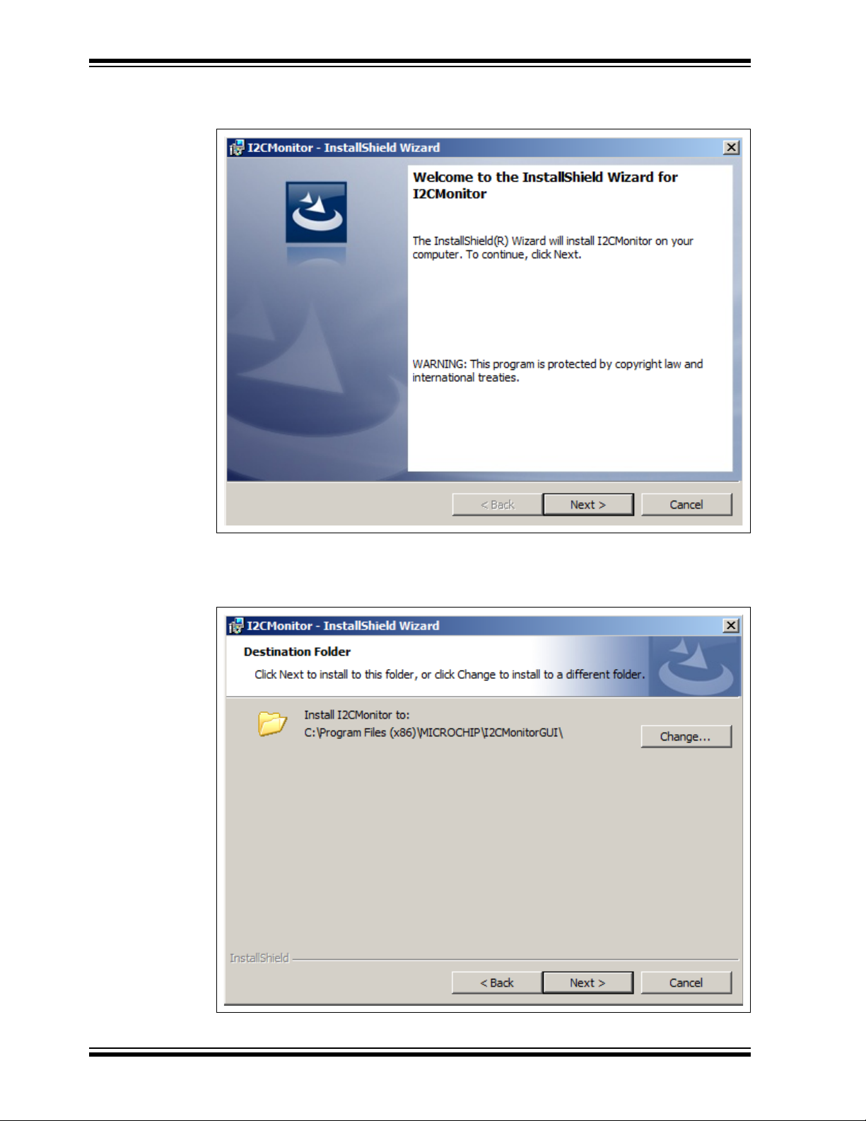
6. In the Welcome to the InstallShield Wizard for I2CMonitor window, click the Next
button to start the installation.
FIGURE 3-1: Starting the I
7. The installation path can be changed, although it is recommended to keep the
default path. Click Next to continue.
2
C Monitor Graphical User Interface Installation.
FIGURE 3-2: Selecting the Destination Folder.
DS50002914A-page 18 2019 Microchip Technology Inc.
Page 19

GUI Installation and Operation
8. In the Ready to Install the Program window, click the Install button and wait for
the application to proceed with the installation. The progress can be observed in
the “Status” bar.
.
FIGURE 3-3: Installing the I2C Monitor Graphical User Interface.
2019 Microchip Technology Inc. DS50002914A-page 19
Page 20
MIC33M656 Evaluation Board User’s Guide
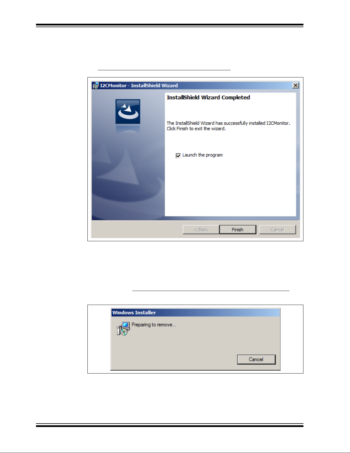
9. Once the installation is complete, leave the “Launch the program” box checked
to automatically start the I
GUI at a later stage. Click Finish to end the installation.
To start the GUI at a later stage, either click the desktop icon or browse to
Windows Start>All Programs>Microchip>I2C Monitor
2
C Monitor GUI or deselect this check box to start the
.
FIGURE 3-4: The Installation Complete Window.
3.3 I2C MONITOR GRAPHICAL USER INTERFACE UNINSTALL
In order to install a new version of the I2C Monitor Graphical User Interface, any
previous version or corrupted version should be removed from the computer.
To uninstall, go to Windows Start>Control Panel>Uninstall a program>I2CMonitor
2
I
C Monitor GUI will automatically close once the uninstallation process is complete.
FIGURE 3-5: Uninstalling the I
2
C Monitor Graphical User Interface.
. The
DS50002914A-page 20 2019 Microchip Technology Inc.
Page 21
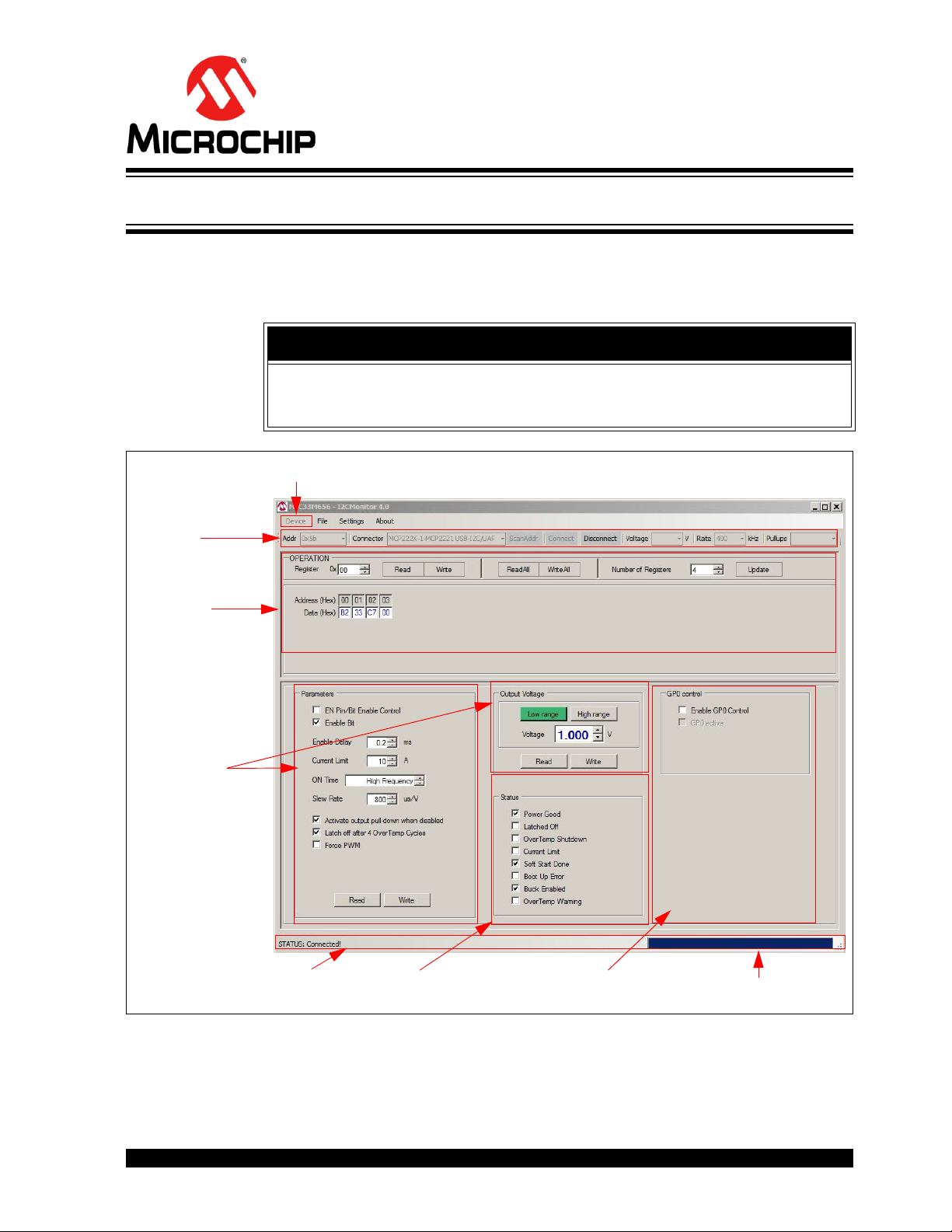
4.1 INTRODUCTION
Device Menu
I
2
C Monitor
Status and
Control Bar
I2C Generic
Register View
MIC33M656 I
2
C
Programmable
Features
Status Bar
MIC33M656 I2C
Diagnostic
MIC33M656
Control by MCP2221 GP0 Output
Progress Bar
This chapter describes how to use the I2C Monitor Graphical User Interface, using the
MIC33M656 Evaluation Board included in the kit.
MIC33M656
EVALUATION BOARD
USER’S GUIDE
Chapter 4. GUI Description
NOTICE
This chapter provides information regarding the use of the GUI only in the case of the
MIC33M656 device. For other devices using the I
see their specific Data Sheets and User’s Guides.
2
C Monitor Graphical User Interface,
2
FIGURE 4-1: I
2019 Microchip Technology Inc. DS50002914A-page 21
C Monitor Graphical User Interface Main Window – MIC33M656 View.
Page 22
MIC33M656 Evaluation Board User’s Guide
4.2 THE GRAPHICAL USER INTERFACE
The following sections describe the items in the Graphical User Interface.
4.2.1 Device Menu
The Device drop-down menu allows the user to select the device to be evaluated. If an
Evaluation (or added custom) Board is used, the profile will automatically change to the
preselected profile.
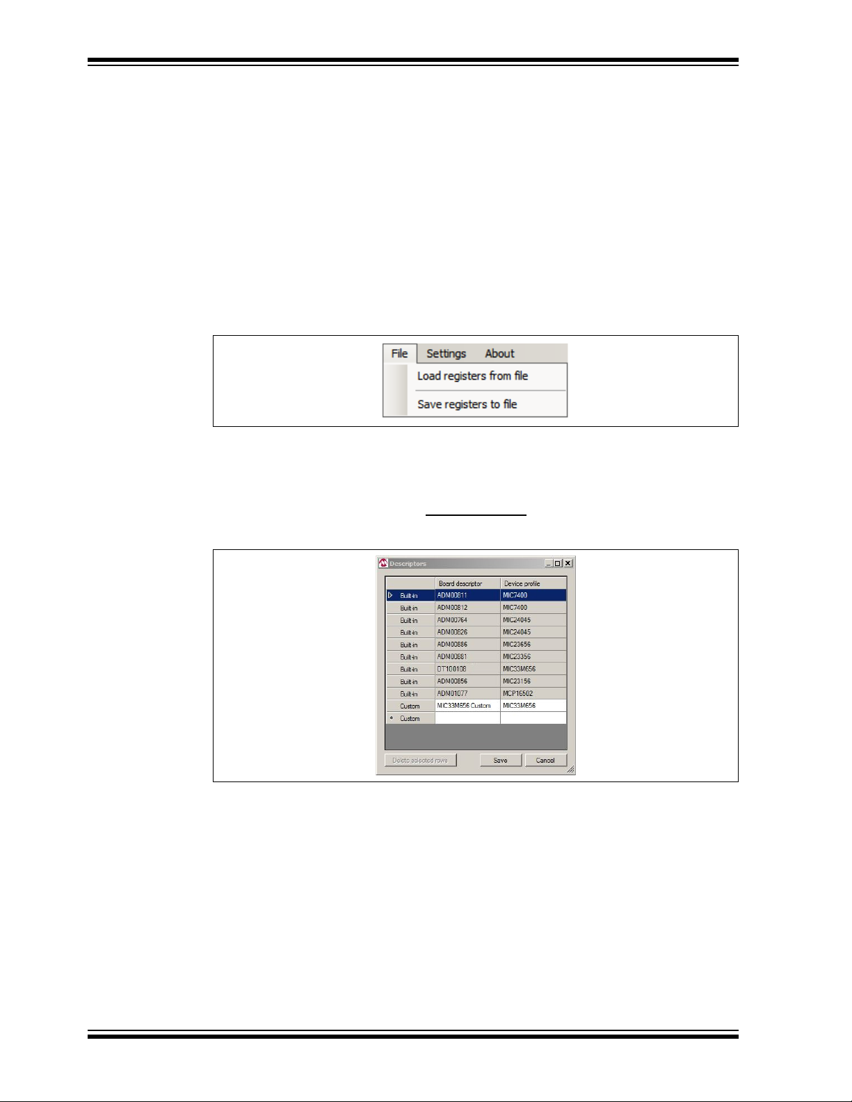
4.2.2 File Menu
The File menu allows the user to save (“Save registers to file”) the registers of the
currently selected device to a file that can then be loaded into the GUI by using the
Load registers from file button. The saved file can also be edited (open it with a text
editor).
FIGURE 4-2: File Menu.
4.2.3 Settings Menu
From the Settings menu, add a new custom board to be automatically detected and
switch to its profile. To do this, go to Settings>Device
window, add the desired “Board” descriptor and select the desired “Device” profile.
FIGURE 4-3: Custom Board Menu.
descriptors, and in the Descriptors
DS50002914A-page 22 2019 Microchip Technology Inc.
Page 23

GUI Description
4.2.4 I2C Monitor Status and Control Bar
The Status and Control bar contains the items listed in Ta b le 4 -1 .
FIGURE 4-4: I
2
C Monitor Status and Control Bar.
TABLE 4-1: MONITOR STATUS AND CONTROL BAR
Item Description
Addr This drop-down menu shows the address of the available devices.
Connector This drop-down menu shows the type of connector used to connect the board.
ScanAddr This button is used to scan for a valid address.
Connect/Disconnect
Voltage This drop-down menu is used to select the voltage level of the communication when using
Rate This drop-down menu is used to select the corresponding communication rate for the
Pull Ups
Note 1: Optional. PICkit Serial Analyzer should first be connected on the I2C pin header on the MIC33M656
Evaluation Board.
These buttons are used to connect/disconnect the current selected device.
the PICkit™ Serial Analyzer.
device.
This drop-down menu is used to activate the internal pull-ups from the PICkit
Serial Analyzer.
(1)
(1)
In the Status and Control bar, the user can choose the hardware tool for communication
with the device and the settings it should allow.
In order to connect to a device, the user must follow the steps described in
Section 2.3 “Getting Started”. After connecting the Micro-USB cable, the user must
scan for a valid address. Once a valid address is detected, clicking the Connect button
will initialize the connection with the device, and the registers will be available for read
and write operations.
2019 Microchip Technology Inc. DS50002914A-page 23
Page 24
MIC33M656 Evaluation Board User’s Guide
4.2.5 I2C Generic Register View
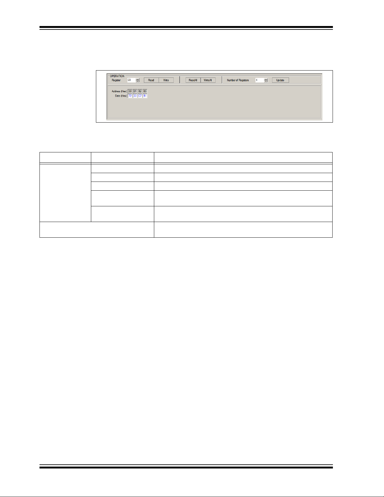
The I2C Generic Register View area contains the items listed in Tab le 4- 2. This section
of the I
FIGURE 4-5: Generic Register View Area.
TABLE 4-2: I2C GENERIC REGISTER VIEW ITEMS
Panel Item Description
Operation Register This section shows the registers available for read/write operations.
Read/Write These buttons are used for single register read/write operations.
ReadAll/WriteAll These buttons are used for reading/writing all the available registers.
Number of Registers In this section, the user can set the number of available registers for
Update This button sets the number of available registers for read/write
Register area This section shows the current status of the registers’ address and
2
C Monitor GUI is common for any device that is evaluated.
read/write operations.
operations in the register area.
their content.
The specific registers for MIC33M656 are described in Appendix C. “MIC33M656
Internal Registers”.
DS50002914A-page 24 2019 Microchip Technology Inc.
Page 25
GUI Description
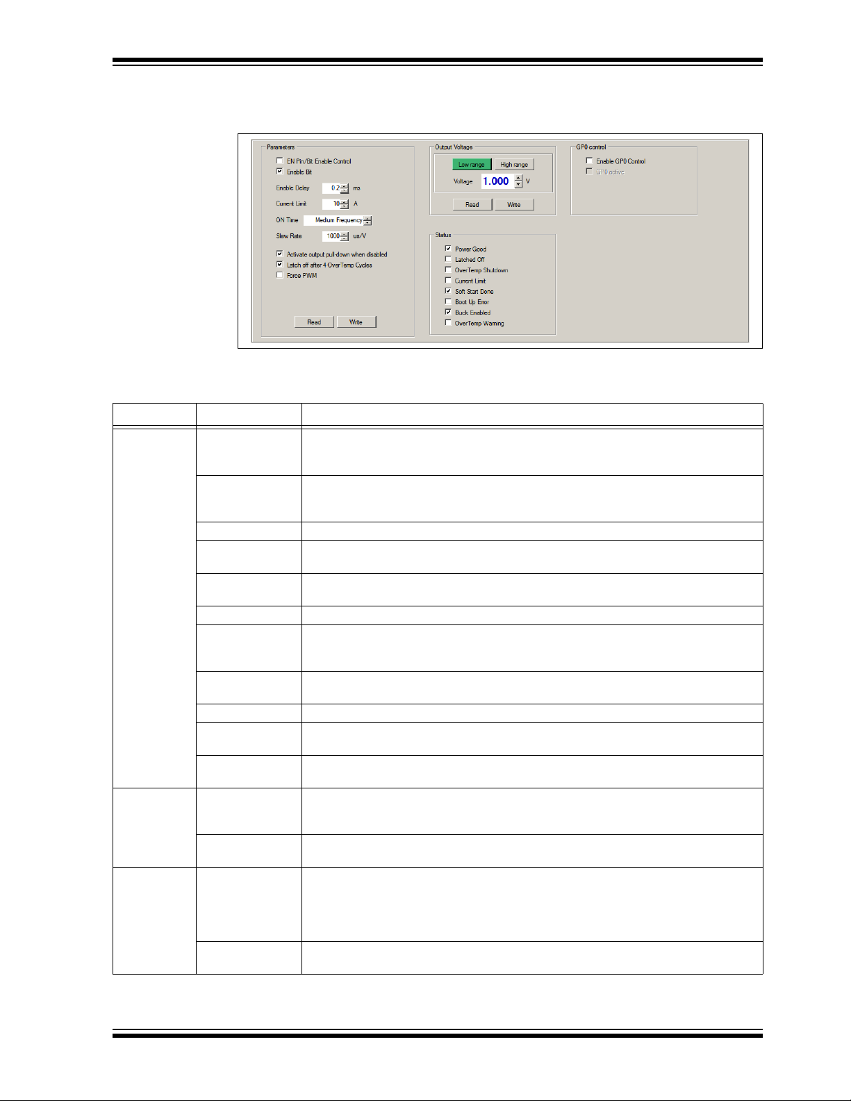
4.2.6 MIC33M656 I2C Programmable Features
The MIC33M656 I2C Programmable Features area contains the items listed in Table 4-3.
2
FIGURE 4-6: MIC33M656 I
TABLE 4-3: MIC33M656 I2C PROGRAMMABLE FEATURES
Panel/Button Items Description
Parameters EN Pin/Bit Enable
Control
Enable Bit This check box sets the MIC33M656 Enable Bit register. Check the box for regulator
Enable Delay This spin box allows setting the available start time delays.
Current Limit This spin box allows setting the available high-side current limits in order to obtain the
ON Time This spin box allows setting the available on-time values that determine slower (high
Slew Rate This spin box allows setting the available output slew rates.
Activate output
pull-down when
disabled
Latch off after
4 OverTemp Cycles
Force PWM This check box sets forced PWM mode, regardless of output loading.
Disable 100% Duty
Cycle
Read/Write These buttons are used to read/write the registers that contain the information
Output Voltage Voltage This spin box allows setting the available output voltages. If the evaluated chip option is
Read/Write These buttons are used to read/write the registers that contain the information
GP0 control Enable GP0
Control
GP0 active This check box sets the state of the MCP2221 GP0 pin. Leave unchecked to disable the
This check box allows switching between the I
and pin controlled enable (unchecked). Leave this box unchecked to enable by jumper
or MCP2221 GP0.
enabling, uncheck for disabling. This bit value is considered only if EN Pin/Bit Enable
Control is checked.
nominal load currents.
T
) or faster (lower TON) switching frequencies.
ON
This check box activates the automatic output pull-down resistor when the MIC33M656
is disabled.
This check box sets the latch off after four overtemperature (thermal shutdown) cycles.
This check box disables 100% duty cycle operation on the high side when V
V
. This feature is available only in High-Range mode (option MIC33M656-SAYMP).
OUT
described above.
MIC33M656-HAYMP or MIC33M656-FAYMP, the Low Range option must be selected. If
the evaluated chip is MIC33M656-SAYMP, the High Range must be selected.
described above.
This check box allows enable control from the MCP2221 GP0 pin. If unchecked, pin
GP0 is tri-state.
To enable access to this feature and allow pin enable control, uncheck EN Pin/Bit
Enable Control.
The enable jumper must first be removed to prevent short circuiting GP0 with the jumper.
MIC33M656 through Enable pin or check the box to enable the MIC33M656 regulator.
This area of the GUI allows the user to modify the device features. For additional
information on the part, refer to the data sheet.
C Programmable Features Area.
2
C controlled device enable (checked)
is close to
IN
2019 Microchip Technology Inc. DS50002914A-page 25
Page 26

MIC33M656 Evaluation Board User’s Guide
4.2.7 MIC33M656 I2C Diagnostic
The MIC33M656 Diagnostic area contains the items listed in Ta b le 4 - 4.
2
FIGURE 4-7: MIC33M656 I
TABLE 4-4: MIC33M656 I2C DIAGNOSTIC AREA ITEMS
Panel Items Description
Status Power Good This box is checked if the output voltage reaches 91% of its set
value.
Latched Off This box is checked if the regulator output is latched off due to four
consecutive hiccup events or thermal shutdown.
OverTemp Shutdown This box is checked if the MIC33M656 enters Thermal Shutdown
(typical, T
Current Limit This box is checked if the high-side sensed current reaches the
value set in the “Current Limit” spin box.
Soft Start Done This box is checked after a successful regulator soft start ramp.
Boot Up Error This box is checked if an error occurs while loading the trim and
configuration data into the digital core. At successful start-up, this
box remains unchecked (clear).
Buck Enabled This box indicates the internal state of the regulator determined by
enable commands (via the EN pin or I
OverTemp Warning This box is checked if the MIC33M656 junction temperature
exceeds +118°C. This does not affect the normal operation of the
device.
C Diagnostic Area.
= +165°C).
J
2
C).
The MIC33M656 I2C Diagnostic area resumes the information contained in the STATUS
Register. The STATUS Register contains latched (Flag) or non-latched (Status) bits. Flag
bits are set when the corresponding Fault condition occurs and do not return to zero once
the Fault condition ceases. If such a Fault occurs, the user can clear the Faults by
toggling the enable function or power cycling the device. Status bits are set when the
corresponding Fault condition has occurred and return to zero automatically once the
Fault condition has ceased. This information is refreshed once every two seconds.
Because of this refresh traffic when using a logic analyzer, it is more difficult to
synchronize the exact moment of a certain command. In order to simplify this, an
auxiliary trigger signal is provided on pin GP2 of the MCP2221. This signal is triggered
for each user Read/Write command.
DS50002914A-page 26 2019 Microchip Technology Inc.
Page 27
GUI Description
TABLE 4-5: STATUS BAR ITEMS
Item Description
Status Label The status label shows if there is any device connected to the board. Refer to Table 4-6 for a list of
possible labels.
Progress Bar This bar shows the level of completion for a given command.
TABLE 4-6: STATUS LABELS
Status Label Description
STATUS: Connected! This message is shown when the GUI connects to a device.
STATUS: Disconnected! This message is shown when the GUI does not detect a connected device.
2019 Microchip Technology Inc. DS50002914A-page 27
Page 28

MIC33M656 Evaluation Board User’s Guide
NOTES:
DS50002914A-page 28 2019 Microchip Technology Inc.
Page 29

Appendix A. Schematic and Layouts
A.1 INTRODUCTION
This appendix contains the following schematic and layouts for the MIC33M656
Evaluation Board:
• Board – Schematic
• Board – Top Silk
• Board – Top Copper and Silk
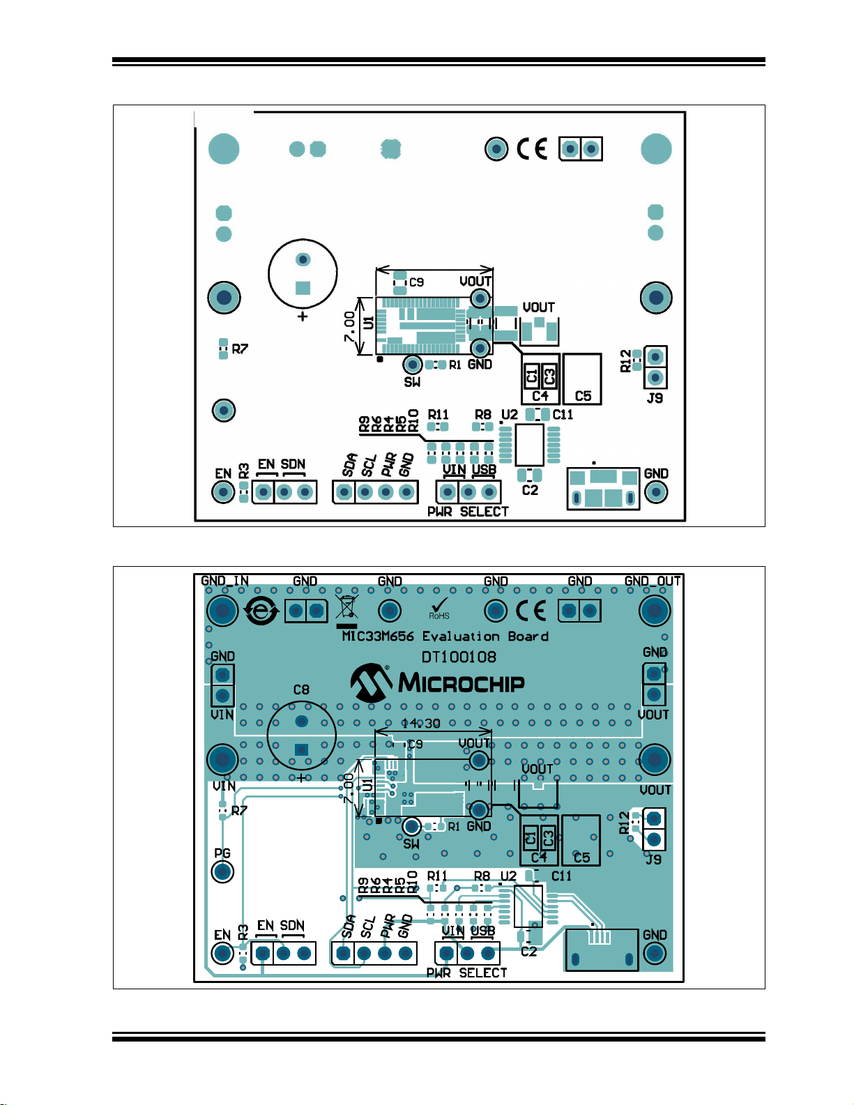
• Board – Top Copper
• Board – Signal Layer 1
• Board – Signal Layer 2
• Board – Bottom Copper
• Board – Bottom Copper and Silk
• Board – Bottom Silk
MIC33M656
EVALUATION BOARD
USER’S GUIDE
2019 Microchip Technology Inc. DS50002914A-page 29
Page 30

DS50002914A-page 30 2019 Microchip Technology Inc.
J15 J19
J20
TP LOOP Red
J21
TP LOOP Red
J14
J18
GND
2k
0603
R6
100k
0603
R7
SDA
49.9R
0603
R1
1 2
J3
J17
470 μF
16V
C8
1
2
3
HDR-2.54 Male 1x3
J6
1
2
J1
J4
J5
47 μF
10V
1210
DNP
C4
47 μF
10V
1210
DNP
C5
12
J1312J12
GND
SW
2k
0603
R9
1M
0603
R3
SCL
PWR
Net Tie
0.5 mm
NT1
AGND GND
DD+
GNDGND
GND
0R
R8
0R
R11
SCL
SDA
EN
PG
V
IN
1
2
3
HDR-2.54 Male 1x3
J8
PWR
0R
R5
0R
R4
V
DD
1
GP0
2
GP1
3
RST
4
UART RX
5
UART TX
6
GP2
7
GP3
8
SDA
9
SCL
10
V
USB
11
D-
12
D+
13
V
SS
14
MCP2221A
U2
GND
DD+
GND
ID
4
V
BUS
1
GND
5
D-
2
D+
3
0
USB 2.0 Micro-B Female
J7
GND
SCL
SDA
1234
J2
PWR
4.7 μF
10V
0805
C2
4.7 μF
10V
0805
C11
10R
0603
1%
R12
1
2
DNP
J9
22 μF
10V
0805
C9
JP1
JP2
0R
DNP
R10
JP2 should be mounted on 1-2 pins J8
GND
GND
V
IN
V
IN
EN
V
IN
GND
PG
AGND
JP1 should be mounted on 1-2 pins J6
GNDGND
GND
GND
GND GND
PWR
47 μF
10V
0805
C1
47 μF
10V
0805
C3
GND GND
J10
U.FL
GND
PGND
2
AUX_AGND
47
PGND
4
SW
14
PV
IN
42
PGND
40
PG
50
SDA
48
AUX_PV
IN
1
EN
49
SW
6
OUT
38
SW
21
AUX_AGND
46
PGND
39
SW
10
V
OUT
51
PGND
3
SCL
45
PGND
5
SW
7
SW
8
AGND
52
SW
11
SW
12
OUT
31
OUT
32
OUT
33
OUT
34
SW
15
SW
16
SW
17
SW
18
SW
19
SW
22
PGND
23
PGND
24
OUT
25
OUT
26
OUT
27
OUT
28
OUT
29
OUT
37
OUT
36
PV
IN
41
SV
IN
43
SV
IN
44
SW
9
SW
13
SW
20
OUT
30
OUT
35
AUX_PV
IN
53
EP (PGND)
54
EP (SW)
55
EP (PGND)56EP (OUT)
57
EP (PGND)
58
EP (PVIN)
59
MIC33M656
U1
VOUT_TP
GND_TP
A.2 BOARD – SCHEMATIC
MIC33M656 Evaluation Board User’s Guide
Page 31
A.3 BOARD – TOP SILK
(
Schematic and Layouts
A.4 BOARD – TOP COPPER AND SILK
2019 Microchip Technology Inc. DS50002914A-page 31
Page 32
MIC33M656 Evaluation Board User’s Guide
A.5 BOARD – TOP COPPER
A.6 BOARD – SIGNAL LAYER 1
DS50002914A-page 32 2019 Microchip Technology Inc.
Page 33
A.7 BOARD – SIGNAL LAYER 2
Schematic and Layouts
A.8 BOARD – BOTTOM COPPER
2019 Microchip Technology Inc. DS50002914A-page 33
Page 34
MIC33M656 Evaluation Board User’s Guide
A.9 BOARD – BOTTOM COPPER AND SILK
A.10 BOARD – BOTTOM SILK
DS50002914A-page 34 2019 Microchip Technology Inc.
Page 35

EVALUATION BOARD
USER’S GUIDE
Appendix B. Bill of Materials (BOM)
MIC33M656
TABLE B-1: BILL OF MATERIALS (BOM)
Qty. Reference Description Manufacturer Part Number
2 C1, C3 Capacitor, Ceramic, 47 µF, 10V,
20%, X5R, SMD, 0805
2 C2, C11 Capacitor, Ceramic, 4.7 µF, 10V,
10%, X7R, SMD, 0805
1 C8 Capacitor, Aluminum, 470 µF,
16V, 20%, RAD, P3.5D8H11.5
1 C9 Capacitor, Ceramic, 22 µF, 10V,
20%, X7S, SMD, 0805
4 J1, J3, J12, J13 Connector, Header, 2.54 Male,
1x2, Gold, 5.84 MH, TH, Vertical
1 J2 Connector, Header, 2.54 Male,
1x4, Tin, 5.84 MH, TH, Vertical
4 J4, J5, J15, J19 Connector, TP, Pin, Tin, TH Harwin Plc. H2121-01
2 J6, J8 Connector, Header, 2.54 Male,
1x3, Tin, 5.84 MH, TH, Vertical
1 J7 Connector, USB 2.0, Micro-B,
Female, SMD, R/A
1 J10 Connector, RF, Coaxial,
Ultra Miniature, Male, SMD, Vertical
2 J14, J21 Miscellaneous, Test Point,
Multipurpose, Mini, Red
3 J17, J18, J20 Miscellaneous, Test Point,
Multipurpose, Mini, Black
1 R1 Resistor, TKF, 49.9R, 1%, 1/10W,
SMD, 0603
1 R3 Resistor, TKF, 1M, 1%, 1/10W,
SMD, 0603
4 R4, R5, R8, R11 Resistor, TKF, 0R, 1/10W, SMD,
0603
2 R6, R9 Resistor, TKF, 2k, 1%, 1/10W,
SMD, 0603
1 R7 Resistor, TKF, 100k, 1%, 1/10W,
SMD, 0603
1 R12 Resistor, TKF, 10R, 1%, 1/10W,
SMD, 0603
1 U1 Microchip Analog Switcher Buck,
0.6V to 3.3V, 6A,
MIC33M656-HAYMP-TR, QFN-53
1 U2 Microchip Interface, USB, I
UART, MCP2221A-I/ST,
TSSOP-14
(1)
TDK Corporation C2012X5R1A476M125AC
TDK Corporation C2012X7R1A475K125AC
Nichicon Corporation UVZ1C471MPD
TDK Corporation C2012X7S1A226M125AC
Amphenol ICC 77311-118-02LF
Amphenol FCI 68002-404HLF
Samtec, Inc. TSW-103-07-T-S
Amphenol ICC 10118193-0001LF
Hirose Electric Co., Ltd. U.FL-R-SMT-1(10)
Keystone Electronics
Corp.
Keystone Electronics
Corp.
Panasonic
Panasonic ERJ-3EKF1004V
Panasonic ERJ-3GEY0R00V
Panasonic ERJ-3EKF2001V
Panasonic ERJ3EKF1003V
Panasonic ERJ3EKF10R0V
Microchip Technology Inc. MIC33M656-HAYMP
2
C,
Microchip Technology Inc. MCP2221A-I/ST
®
ERJ3EKF49R9V
5000
5001
2019 Microchip Technology Inc. DS50002914A-page 35
Page 36

MIC33M656 Evaluation Board User’s Guide
TABLE B-1: BILL OF MATERIALS (BOM)
Qty. Reference Description Manufacturer Part Number
2 JP1, JP2 Mechanical Hardware, Jumper,
2.54 mm, 1x2
1 LABEL1 Label, Assembly w/Revision Level
(Small Modules) per MTS-0002
4PAD1, PAD2,
PAD3, PAD4
1 PCB1 Printed Circuit Board Microchip Technology Inc. 04-11021-R1
0C4, C5 DO NOT POPULATE Taiyo Yuden Co., Ltd. LMK325B7476MM-TR
0J9 DO NOT POPULATE Amphenol ICC 77311-118-02LF
0R10 DO NOT POPULATE Panasonic
Note 1: The components listed in this Bill of Materials are representative of the PCB assembly. The released BOM
used in manufacturing uses all RoHS-compliant components.
Mechanical Hardware, Rubber
Pad, Cylindrical, D7.9, H5.3,
Black
(1)
(CONTINUED)
3M 969102-0000-DA
3M 70006431483
——
®
ERJ-3GSY0R00V
DS50002914A-page 36 2019 Microchip Technology Inc.
Page 37
EVALUATION BOARD
Appendix C. MIC33M656 Internal Registers
C.1 REGISTER MAP AND I2C PROGRAMMABILITY
The MIC33M656 internal registers are summarized in Ta bl e C - 1 .
TABLE C-1: MIC33M656 REGISTER MAP
Address Register Name
0x00 Control Register (CTRL1)
TON[1:0] ILIM[1:0] EN_DELAY[1:0] EN_INT EN_CON
0x01 Output Control Register (CTRL2)
DIS_100PCT FPWM OT_LATCH PULL_DN SLEW_RATE[3:0]
0x02 Output Voltage Control Register (VOUT)
VO[7:0]
0x03 STATUS and Fault Register (FAULT)
OT_WARN EN_STAT BOOT_ERR SSD HICCUP OT LATCH_OFF PG
MIC33M656
USER’S GUIDE
REGISTER C-1: CTRL1: CONTROL REGISTER (ADDRESS 0x00)
R/W-0 R/W-0 R/W-0 R/W-0 R/W-0 R/W-0 R/W-0 R/W-0
TON[1:0] ILIM[1:0] EN_DELAY[1:0] EN_INT EN_CON
bit 7 bit 0
Legend:
R = Readable bit W = Writable bit U = Unimplemented bit, read as ‘0’
-n = Value at POR ‘1’ = Bit is set ‘0’ = Bit is cleared x = Bit is unknown
bit 7-6 TON[1:0]: On Time
00 = Low frequency
01 = Medium frequency
10 = High frequency
11 = Very fast frequency
bit 5-4 ILIM[1:0]: High-Side Peak Current Limit
00 = 4.5A
01 = 6A
10 = 8.5A
11 = 10.0A
bit 3-2 EN_DELAY[1:0]: Enable Delay
00 = 250 µs
01 = 1 ms
10 = 2 ms
11 = 3 ms
bit 1 EN_INT: Enable Bit Register Control
0 = Register controlled
1 = Enable pin controlled
bit 0 EN_CON: Enable Control
0 = Off
1 = On
2019 Microchip Technology Inc. DS50002914A-page 37
Page 38

MIC33M656 Evaluation Board User’s Guide
REGISTER C-2: CTRL2: OUTPUT CONTROL REGISTER (ADDRESS 0x01)
R/W-0 R/W-0 R/W-0 R/W-0 R/W-0 R/W-0 R/W-0 R/W-0
DIS_100PCT FPWM OT_LATCH PULLDN SLEW_RATE[3:0]
bit 7 bit 0
Legend:
R = Readable bit W = Writable bit U = Unimplemented bit, read as ‘0’
-n = Value at POR ‘1’ = Bit is set ‘0’ = Bit is cleared x = Bit is unknown
bit 7 DIS_100PCT: Disable 100% Duty Cycle
0 = 100% DC
1 = Disable 100% DC
bit 6 FPWM: Force PWM
0 = HLL
1 = FPWM
bit 5 OT_LATCH: Overtemperature Latch
0 = Latch off immediately
1 = Latch off after four OT cycles
bit 4 PULLDN: Enable/Disable Regulator Pull Down when Power-Down
0 = No pull down
1 = Pull down
bit 3-0 SLEW_RATE[3:0]: Step Slew Rate Time in µs/V
0000 = 200
0001 = 400
0010 = 600
0011 = 800
0100 = 1000
0101 = 1200
0110 = 1400
0111 = 1600
1000 = 1800
1001 = 2000
1010 = 2200
1011 = 2400
1100 = 2600
1101 = 2800
1110 = 3000
1111 = 3200
DS50002914A-page 38 2019 Microchip Technology Inc.
Page 39
MIC33M656 Internal Registers
0x00-0x76 = 0.6V 0x80 = 0.645 0xA0 = 0.805V 0xC0 = 0.965 0xE0 = 1.125V
0x81 = 0.65V 0xA1 = 0.81V 0xC1 = 0.97V 0xE1 = 1.13V
0x82 = 0.655V 0xA2 = 0.815V 0xC2 = 0.975V 0xE2 = 1.135V
0x83 = 0.66V 0xA3 = 0.82V 0xC3 = 0.98V 0xE3 = 1.14V
0x84 = 0.665V 0xA4 = 0.825V 0xC4 = 0.985V 0xE4 = 1.145V
0x85 = 0.67V 0xA5 = 0.83V 0xC5 = 0.99V 0xE5 = 1.15V
0x86 = 0.675V 0xA6 = 0.835V 0xC6 = 0.995V 0xE6 = 1.155V
0x87 = 0.68V 0xA7 = 0.84V 0xC7 = 1V 0xE7 = 1.16V
0x88 = 0.685V 0xA8 = 0.845V 0xC8 = 1.005V 0xE8 = 1.165V
0x89 = 0.69V 0xA9 = 0.85V 0xC9 = 1.01V 0xE9 = 1.17V
0x8A = 0.695V 0xAA = 0.855V 0xCA = 1.015V 0xEA = 1.175V
0x8B = 0.7V 0xAB = 0.86V 0xCB = 1.02V 0xEB = 1.18V
0x8C = 0.705V 0xAC = 0.865V 0xCC = 1.025V 0xEC = 1.185V
0x8D = 0.71V 0xAD = 0.87V 0xCD = 1.03V 0xED = 1.19V
0x8E = 0.715V 0xAE = 0.875V 0xCE = 1.035V 0xEE = 1.195V
0x8F = 0.72V 0xAF = 0.88V 0xCF = 1.04V 0xEF = 1.2V
0x90 = 0.725V 0xB0 = 0.885V 0xD0 = 1.045V 0xF0 = 1.205V
0x91 = 0.73V 0xB1 = 0.89V 0xD1 = 1.05V 0xF1 = 1.21V
0x92 = 0.735V 0xB2 = 0.895V 0xD2 = 1.055V 0xF2 = 1.215V
0x93 = 0.74V 0xB3 = 0.9V 0xD3 = 1.06V 0xF3 = 1.22V
0x94 = 0.745V 0xB4 = 0.905V 0xD4 = 1.065V 0xF4 = 1.225V
0x95 = 0.75V 0xB5 = 0.91V 0xD5 = 1.07V 0xF5 = 1.23V
0x96 = 0.755V 0xB6 = 0.915V 0xD6 = 1.075V 0xF6 = 1.235V
0x77 = 0.6V 0x97 = 0.76V 0xB7 = 0.92V 0xD7 = 1.08V 0xF7 = 1.24V
0x78 = 0.605V 0x98 = 0.765V 0xB8 = 0.925V 0xD8 = 1.085V 0xF8 = 1.245V
0x79 = 0.61V 0x99 = 0.77V 0xB9 = 0.93V 0xD9 = 1.09V 0xF9 = 1.25V
0x7A = 0.615V 0x9A = 0.775V 0xBA = 0.935V 0xDA = 1.095V 0xFA = 1.255V
0x7B = 0.62V 0x9B = 0.78V 0xBB = 0.94V 0xDB = 1.1V 0xFB = 1.26V
0x7C = 0.625V 0x9C = 0.785V 0xBC = 0.945V 0xDC = 1.105V 0xFC = 1.265V
0x7D = 0.63V 0x9D = 0.79V 0xBD = 0.95V 0xDD = 1.11V 0xFD = 1.27V
0x7E = 0.635V 0x9E = 0.795V 0xBE = 0.955V 0xDE = 1.115V 0xFE = 1.275V
0x7F = 0.64V 0x9F = 0.8V 0xBF = 0.96V 0xDF = 1.12V 0xFF = 1.28V
REGISTER C-3: VOUT: OUTPUT VOLTAGE CONTROL REGISTER (ADDRESS 0x02)
R/W-0 R/W-0 R/W-0 R/W-0 R/W-0 R/W-0 R/W-0 R/W-0
VO[7:0]
bit 7 bit 0
Legend:
R = Readable bit W = Writable bit U = Unimplemented bit, read as ‘0’
-n = Value at POR ‘1’ = Bit is set ‘0’ = Bit is cleared x = Bit is unknown
bit 7-0 VO[7:0]: Output Voltage Control (-HAYMP, -FAYMP options)
2019 Microchip Technology Inc. DS50002914A-page 39
Page 40

MIC33M656 Evaluation Board User’s Guide
REGISTER C-3: VOUT: OUTPUT VOLTAGE CONTROL REGISTER (ADDRESS 0x02) (CONTINUED)
bit 7-0 VO[7:0]: Output Voltage Control (-SAYMP option)
0x00-0x3B = 0.6V 0x40 = 0.65V 0x60 = 0.97V 0x80 = 1.3V 0xA0 = 1.94V 0xC0 = 2.58V 0xE0 = 3.22V
0x41 = 0.66V 0x61 = 0.98V 0x81=1.32V 0xA1 = 1.96V 0xC1 = 2.6V 0xE1 = 3.24V
0x42 = 0.67V 0x62 = 0.99V 0x82 = 1.34V 0xA2 = 1.98V 0xC2 = 2.62V 0xE2 = 3.26V
0x43 = 0.68V 0x63 = 1V 0x83 = 1.36V 0xA3 = 2V 0xC3 = 2.64V 0xE3 = 3.28V
0x44 = 0.69V 0x64 = 1.01V 0x84 = 1.38V 0xA4 = 2.02V 0xC4 = 2.66V 0xE4 = 3.3V
0x45 = 0.7V 0x65 = 1.02V 0x85 = 1.4V 0xA5 = 2.04V 0xC5 = 2.68V 0xE5 = 3.32V
0x46 = 0.71V 0x66 = 1.03V 0x86 = 1.42V 0xA6 = 2.06V 0xC6 = 2.7V 0xE6 = 3.34V
0x47 = 0.72V 0x67 = 1.04V 0x87 = 1.44V 0xA7 = 2.08V 0xC7 = 2.72V 0xE7 = 3.36V
0x48 = 0.73V 0x68 = 1.05V 0x88 = 1.46V 0xA8 = 2.1V 0xC8 = 2.74V 0xE8 = 3.38V
0x49 = 0.74V 0x69 = 1.06V 0x89 = 1.48V 0xA9 = 2.12V 0xC9 = 2.76V 0xE9 = 3.4V
0x4A = 0.75V 0x6A = 1.07V 0x8A = 1.5V 0xAA = 2.14V 0xCA = 2.78V 0xEA = 3.42V
0x4B = 0.76V 0x6B = 1.08V 0x8B = 1.52V 0xAB = 2.16V 0xCB = 2.8V 0xEB = 3.44V
0x4C = 0.77V 0x6C = 1.09V 0x8C = 1.54V 0xAC = 2.18V 0xCC = 2.82V 0xEC = 3.46V
0x4D = 0.78V 0x6D = 1.1V 0x8D = 1.56V 0xAD = 2.2V 0xCD = 2.84V 0xED = 3.48V
0x4E = 0.79V 0x6E = 1.11V 0x8E = 1.58V 0xAE = 2.22V 0xCE = 2.86V 0xEE = 3.5V
0x4F = 0.8V 0x6F=1.12V 0x8F = 1.6V 0xAF = 2.24V 0xCF = 2.88V 0xEF = 3.52V
0x50 = 0.81V 0x70 = 1.13V 0x90 = 1.62V 0xB0 = 2.26V 0xD0 = 2.9V 0xF0 = 3.54V
0x51 = 0.82V 0x71 = 1.14V 0x91 = 1.64V 0xB1 = 2.28V 0xD1 = 2.92V 0xF1 = 3.56V
0x52 = 0.83V 0x72 = 1.15V 0x92 = 1.66V 0xB2 = 2.3V 0xD2 = 2.94V 0xF2 = 3.58V
0x53 = 0.84V 0x73 = 1.16V 0x93 = 1.68V 0xB3 = 2.32V 0xD3 = 2.96V 0xF3 = 3.6V
0x54 = 0.85V 0x74 = 1.17V 0x94 = 1.7V 0xB4 = 2.34V 0xD4 = 2.98V 0xF4 = 3.62V
0x55 = 0.86V 0x75 = 1.18V 0x95 = 1.72V 0xB5 = 2.36V 0xD5 = 3V 0xF5 = 3.64V
0x56 = 0.87V 0x76=1.19V 0x96 = 1.74V 0xB6 = 2.38V 0xD6 = 3.02V 0xF6 = 3.66V
0x57 = 0.88V 0x77 = 1.2V 0x97 = 1.76V 0xB7 = 2.4V 0xD7 = 3.04V 0xF7 = 3.68V
0x58 = 0.89V 0x78 = 1.21V 0x98 = 1.78V 0xB8 = 2.42V 0xD8 = 3.06V 0xF8 = 3.7V
0x59 = 0.9V 0x79 = 1.22V 0x99 = 1.8V 0xB9 = 2.44V 0xD9 = 3.08V 0xF9 = 3.72V
0x5A = 0.91V 0x7A = 1.23V 0x9A = 1.82V 0xBA = 2.46V 0xDA = 3.1V 0xFA = 3.74V
0x3B = 0.6V 0x5B = 0.92V 0x7B = 1.24V 0x98 = 1.84V 0xBB = 2.48V 0xDB = 3.12V 0xFB = 3.76V
0x3C = 0.61V 0x5C = 0.93V 0x7C = 1.25V 0x9C = 1.86V 0xBC = 2.5V 0xDC = 3.14V 0xFC = 3.78V
0x3D = 0.62V 0x5D = 0.94V 0x7D = 1.26V 0x9D = 1.88V 0xBD = 2.52V 0xDD = 3.16V 0xFD = 3.8V
0x3E = 0.63V 0x5E = 0.95V 0x7E = 1.27V 0x9E = 1.9V 0xBE = 2.54V 0xDE = 3.18V 0xFE = 3.82V
0x3F = 0.64V 0x5F = 0.96V 0x7F = 1.28V 0x9F = 1.92V 0xBF = 2.56V 0xDF = 3.2V 0xFF = 3.84V
DS50002914A-page 40 2019 Microchip Technology Inc.
Page 41

MIC33M656 Internal Registers
REGISTER C-4: FAULT: STATUS AND FAULT REGISTER (ADDRESS 0x03)
R-0 R-0 R-0 R-0 R-0 R-0 R-0 R-0
OT_WARN EN_STAT BOOT_ERR SSD HICCUP OT LATCH_OFF PG
bit 7 bit 0
Legend:
R = Readable bit W = Writable bit U = Unimplemented bit, read as ‘0’
-n = Value at POR ‘1’ = Bit is set ‘0’ = Bit is cleared x = Bit is unknown
bit 7 OT_WARN: Overtemperature Warning
0 = No Fault
1 = Fault
bit 6 EN_STAT: Buck On/Off Control
0 = Off
1 = On
bit 5 BOOT_ERR: Boot-up Error
0 = No Fault
1 = Fault
bit 4 SSD: Soft Start Done
0 = Ramp not done
1 = Ramp done
bit 3 HICCUP: Current Limit Hiccup
0 = Not in Hiccup mode
1 = In Hiccup mode
bit 2 OT: Overtemperature
0 = No Fault
1 = Fault
bit 1 LATCH_OFF: Overcurrent or Overtemperature Output Latch Off
0 = No Fault
1 = Fault
bit 0 PG: Power Good
0 = Power not good
1 = Power good
2019 Microchip Technology Inc. DS50002914A-page 41
Page 42

Worldwide Sales and Service
AMERICAS
Corporate Office
2355 West Chandler Blvd.
Chandler, AZ 85224-6199
Tel: 480-792-7200
Fax: 480-792-7277
Technical Support:
http://www.microchip.com/
support
Web Address:
www.microchip.com
Atlanta
Duluth, GA
Tel: 678-957-9614
Fax: 678-957-1455
Austin, TX
Tel: 512-257-3370
Boston
Westborough, MA
Tel: 774-760-0087
Fax: 774-760-0088
Chicago
Itasca, IL
Tel: 630-285-0071
Fax: 630-285-0075
Dallas
Addison, TX
Tel: 972-818-7423
Fax: 972-818-2924
Detroit
Novi, MI
Tel: 248-848-4000
Houston, TX
Tel: 281-894-5983
Indianapolis
Noblesville, IN
Tel: 317-773-8323
Fax: 317-773-5453
Tel: 317-536-2380
Los Angeles
Mission Viejo, CA
Tel: 949-462-9523
Fax: 949-462-9608
Tel: 951-273-7800
Raleigh, NC
Tel: 919-844-7510
New York, NY
Tel: 631-435-6000
San Jose, CA
Tel: 408-735-9110
Tel: 408-436-4270
Canada - Toronto
Tel: 905-695-1980
Fax: 905-695-2078
ASIA/PACIFIC
Australia - Sydney
Tel: 61-2-9868-6733
China - Beijing
Tel: 86-10-8569-7000
China - Chengdu
Tel: 86-28-8665-5511
China - Chongqing
Tel: 86-23-8980-9588
China - Dongguan
Tel: 86-769-8702-9880
China - Guangzhou
Tel: 86-20-8755-8029
China - Hangzhou
Tel: 86-571-8792-8115
China - Hong Kong SAR
Tel: 852-2943-5100
China - Nanjing
Tel: 86-25-8473-2460
China - Qingdao
Tel: 86-532-8502-7355
China - Shanghai
Tel: 86-21-3326-8000
China - Shenyang
Tel: 86-24-2334-2829
China - Shenzhen
Tel: 86-755-8864-2200
China - Suzhou
Tel: 86-186-6233-1526
China - Wuhan
Tel: 86-27-5980-5300
China - Xian
Tel: 86-29-8833-7252
China - Xiamen
Tel: 86-592-2388138
China - Zhuhai
Tel: 86-756-3210040
ASIA/PACIFIC
India - Bangalore
Tel: 91-80-3090-4444
India - New Delhi
Tel: 91-11-4160-8631
India - Pune
Tel: 91-20-4121-0141
Japan - Osaka
Tel: 81-6-6152-7160
Japan - Tokyo
Tel: 81-3-6880- 3770
Korea - Daegu
Tel: 82-53-744-4301
Korea - Seoul
Tel: 82-2-554-7200
Malaysia - Kuala Lumpur
Tel: 60-3-7651-7906
Malaysia - Penang
Tel: 60-4-227-8870
Philippines - Manila
Tel: 63-2-634-9065
Singapore
Tel: 65-6334-8870
Taiwan - Hsin Chu
Tel: 886-3-577-8366
Taiwan - Kaohsiung
Tel: 886-7-213-7830
Taiwan - Taipei
Tel: 886-2-2508-8600
Thailand - Bangkok
Tel: 66-2-694-1351
Vietnam - Ho Chi Minh
Tel: 84-28-5448-2100
EUROPE
Austria - Wels
Tel: 43-7242-2244-39
Fax: 43-7242-2244-393
Denmark - Copenhagen
Tel: 45-4450-2828
Fax: 45-4485-2829
Finland - Espoo
Tel: 358-9-4520-820
France - Paris
Tel: 33-1-69-53-63-20
Fax: 33-1-69-30-90-79
Germany - Garching
Tel: 49-8931-9700
Germany - Haan
Tel: 49-2129-3766400
Germany - Heilbronn
Tel: 49-7131-72400
Germany - Karlsruhe
Tel: 49-721-625370
Germany - Munich
Tel: 49-89-627-144-0
Fax: 49-89-627-144-44
Germany - Rosenheim
Tel: 49-8031-354-560
Israel - Ra’anana
Tel: 972-9-744-7705
Italy - Milan
Tel: 39-0331-742611
Fax: 39-0331-466781
Italy - Padova
Tel: 39-049-7625286
Netherlands - Drunen
Tel: 31-416-690399
Fax: 31-416-690340
Norway - Trondheim
Tel: 47-7288-4388
Poland - Warsaw
Tel: 48-22-3325737
Romania - Bucharest
Tel: 40-21-407-87-50
Spain - Madrid
Tel: 34-91-708-08-90
Fax: 34-91-708-08-91
Sweden - Gothenberg
Tel: 46-31-704-60-40
Sweden - Stockholm
Tel: 46-8-5090-4654
UK - Wokingham
Tel: 44-118-921-5800
Fax: 44-118-921-5820
DS50002914A-page 42 2019 Microchip Technology Inc.
05/14/19
 Loading...