

查询MCRF200供应商
MCRF200
125 kHz microID™ Passive RFID Device
Features
• Factory programming and memory serialization
• One-time contactless programmable (developer
• Read-only data transmission after programming
• 96 or 128 bits of One-Time Programmable (OTP)
• Typical operation frequency: 100 kHz-400 kHz
• Ultra low-power operation (5 µA @ V
• Modulation options:
• Data Encoding options:
• Die, wafer, COB, PDIP or SOIC package option s
• Factory programming options
SM
(SQTP
kit only)
user memory (also supports 48 and 64-bit
protocols)
- ASK, FSK, PSK
- NRZ Direct, Differential Biphase, Manchester
)
CC = 2V)
Biphase
Application
• Low-cost alternative for existing low-frequency
RFID devices
• Access control and time attendance
• Security systems
• Animal tagging
• Product identification
• Industrial taggin g
• Inventory control
RF
Signal
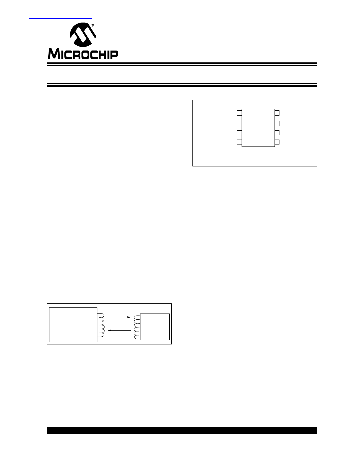
Package Type
PDIP/SOIC
VA VB
1
NC
2
3
I/O
RESET
Note: Pins 3, 4, 5 and 6 are for device test purposes only.
Pins 1 and 8 are for antenna connections.
DO NOT ground pin 5.
4
8
NC
7
6
SS
V
VCC
5
Description
The MCRF200 is a passive Radio Frequency Identification (RFID) device for low-frequency applications
(100 kHz-400 kHz). The device is powered by
rectifying an incoming RF signal from the reader. The
device requires an external LC resonant circuit to
receive th e inco ming RF signal and to s end da ta. The
device develops a sufficient DC voltage for operation
when its external coil voltag e reaches approx imately 10
PP.
V
This device has a total of 128 bits o f user programmable
memory and an additional 12 bits in its configuration
register. The user can manually program the 128 bits of
user memory by using a contactless programmer in a
microID developer kit such as DV103001 or PG103001.
However, in production volume the MCRF200 is
programmed at the factory (Microchip SQTP – see
Technical Bulletin TB023). The device is a One-Time
Programmable (OTP) integrated circuit and operates as
a read-only device after programming.
Reader
Data
2003 Microchip Technology Inc. DS21219H-page 1
MCRF200
MCRF200
Block Diagram
Coil
Connections
Circuit
Modulation
Clock
Generator
Rectifier
V
VSS
CC
Modulation
Control
Row
Decode
Counter
Data
Memory
Array
Column
Decode
The configuration reg is ter i nc lud es op tio ns for communication protocol (ASK, FSK, PSK), data encoding
method, data rate, and data length.These options are
specified by custom er a nd fact ory pr og ramme d dur ing
assembly . Becaus e of its many choices of confi guration
options, the devi ce can be easily used as an alt ernative
or second source for mo st of the existin g low frequenc y
passive RFID devices available today.
The device has a modulation transistor between the
two antenna connections (V
A and VB). The modulation
transistor damps or undamps the coil voltage when it
sends data. The variation of coil voltage controlled by
the modulation transistor results in a perturbation of
voltage in reader antenna coil. By monitoring the
changes in reader coil voltage, the data transmitted
from the device can be reconstructed.
The device is available in die, wafer, Chip-on-Board
(COB) modules, PDIP, or SOIC packages. Factory
programming and memory serialization (SQTP) are
also available upon request. See TB023 for more
information on contact programming support.
The DV103001 developer’s kit includes Contactless
Programmer, ASK, FSK, PSK reference readers, and
reference design guide. The reference design guide
includes schematics for readers and contactless
programmer as well as in-depth document for antenna
circuit designs.
DS21219H-page 2 2003 Microchip Technology Inc.

1.0 ELECTRICAL CHARACTERISTICS
MCRF200
Absolute Maximum Ratings
Storage temperature..............................................................................................................................- 65°C to +150°C
Ambient temperature with power applied................................................................................................-40°C to +125°C
Maximum current into coil pads..............................................................................................................................50 mA
† NOTICE: Stresses above those listed under “Absolute Maximum Ratings” may cause permanent damage to
the device. This is a stress rating only and functional operation of the device at those or any other conditions
above those indica ted in the opera tional li stings of this sp ecificati on is not i mplied. Ex posure to maximum rating
conditions for extended periods may affect device reliability.
(†)
TABLE 1-1: AC AND DC CHARACTERISTICS
All parameters apply across the
specified operating ranges unless
otherwise noted.
Parameter Sym Min Typ Max Units Conditions
Clock frequency FCLK 100 — 400 kHz
Contactless programming time T
Data retention 200 — — Years at 25°C
Coil current (Dynamic) ICD —50 µA
Operating current I
Turn-on-volt a ge (Dyna mic) for
modulation
Input Capacitance CIN — 2 — pF Between VA and VB
Industrial (I): T
WC — 2 — sec For all 128-bit array
DD —5 µAVCC = 2V
VAVB 10 — — VPP
VCC 2——VDC
A = -40°C to +85°C
2003 Microchip Technology Inc. DS21219H-page 3

MCRF200
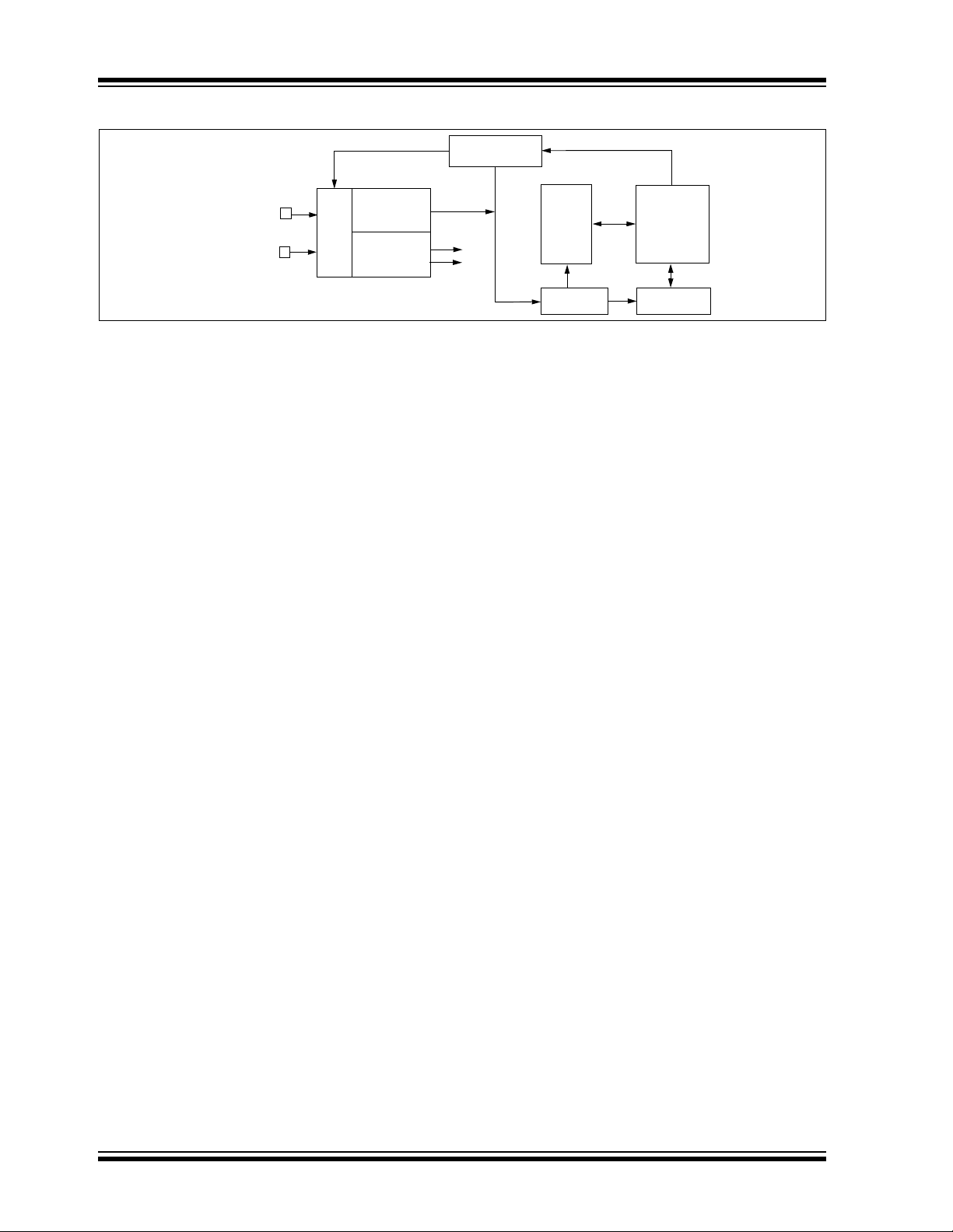
2.0 FUNCTION DESCRIPTION
The device contains three major building blocks. They
are RF front-end, configuration and control logic, and
memory sections. The Block Diagram is shown on
page 1.
2.1 RF Front-End
The RF front-end of the device includes circuits for
rectification of the carrier, V
high-voltage clamping. This section also includes a
clock generator and modulation circuit.
DD (operating voltage) and
2.1.2 POWER-ON RESET
This circuit generates a Power-on Reset when the tag
first enters the reader field. The Reset releases when
sufficient powe r has develope d on the V
allow correct operation.
2.1.3 CLOCK GENERATOR
This circuit generates a clock based on the carrier
frequency from the reader. This clock is used to derive
all timing in the device, including the baud rate and
modulation rate.
2.1.4 MODULATION CIRCUIT
2.1.1 RECTIFIER – AC CLAMP
The rectifier circuit rectifies RF voltage on the external
LC antenna circuit. An y excessi ve volt age on the tuned
circuit is clamped b y the intern al circuit ry to a safe l evel
to prevent damage to the IC.
The device sends the encoded data to the reader by
AM-modulating the coil voltage across the tuned LC
circuit. A modulation transistor is placed between the
two antenna coil pads (V
on and off based on the m odu lat ion sig nal . As a res ul t,
the amplitude of the antenna coil vo ltage varies wi th the
modulation signal. See Figure 2-1 for details.
FIGURE 2-1: MODULATION SIGNAL AND MODULATED SIGNAL
MCRF200
VA
Modulation
Signal
DD regulator to
A and VB). The transistor turns
Amplitude
Modulation Signal
Modulated RF Signal
(across VA and VB)
LC
Modulation
Transistor
VB
t
DS21219H-page 4 2003 Microchip Technology Inc.

MCRF200
2.2 Configuration Register and
Control Logic
The configuration register determines the operational
parameters of the device. The configuration register
can not be programmed contactlessly; it is
programmed during wafer probe at the Microchip
factory. CB11 is always a zero; CB12 is set when
successful contact or contactless programming of the
data array has been completed. Once CB12 is set,
device programmi ng and erasin g is disabled. Table 2-4
contains a descri ptio n of the bi t functions of the control
register.
2.2.1 BAUD RATE TIMING OPTION
The chip will acces s d at a at a ba ud rate determined by
bits CB2, CB3 and CB4 of the configuration register.
For example, MOD32 (CB2 = 0, CB3 = 1, CB4 = 1) has
32 RF cycles per bit. This gives the data rate of 4 kHz
for the RF carrier frequency of 128 kHz.
The default timing is MOD128 (F
mode is used for contact and contactless programming. Once the array is successfully programmed, the
lock bit CB12 is set. When the lock bit is set, programming and erasing the device becomes permanently
disabled. The configu ration register has no effect on
device timing until the EEPROM data array is
programmed (CB12 = 1).
2.2.2 DATA ENCODING OPTION
This logic acts upon the s erial dat a bein g read from th e
EEPROM. The logic encodes the dat a acc ording to th e
configuration bits CB6 and CB7. CB6 and CB7
determine the data encoding method. The available
choices are:
• Non-return to zero-level (NRZ_L)
• Biphase Differential, Biphase Manchester
• Inverted Manchester
CLK/128), and this
2.2.3 MODULATION OPTION
CB8 and CB9 determine the mo dulation pro tocol of the
encoded data. The available choices are:
• ASK
•FSK
• PSK_1
• PSK_2
When ASK (direct) option is chosen, the encoded data
is fed into the modulation transistor without change.
When FSK option is chosen, the encoded data is
represented by:
a) Sets of 10 RF carrier cycles (first 5 cycles →
higher amplitude, the last 5 cycles → lower
amplitude) for logic “high” level.
b) Sets of 8 RF carrier cycles (first 4 cycles →
higher amplitude, the last 4 cycles → lower
amplitude) for logic “low” level.
For example, FSK signal for MOD40 is represented:
a) 4 sets of 10 RF carrier cycles for data ‘1’.
b) 5 sets of 8 RF carrier cycles for data ‘0’.
Refer to Figure 2-2 for the FSK signal with MOD40
option.
The PSK_1 represents change in the phase of the
modulation signal at the change of the encoded data.
For example, the phase changes when the encoded
data is changed from ‘1’ to ‘0’, or from ‘0’ to ‘1’.
The PSK_2 represents change in the phase at the
change on ‘1’. For example, the phase changes when
the encoded data is changed from ‘0’ to ‘1’, or from ‘1’
to ‘1’.
FIGURE 2-2: ENCODED DATA AND FSK OUTPUT SIGNAL FOR MOD40 OPTION
Encoded Data ‘1’
5 cycles (HI)
5 cycles (LO)
40 RF cycles
2003 Microchip Technology Inc. DS21219H-page 5
4 cycles (HI)
Encoded Data ‘0’
4 cycles (LO)
40 RF cycles
MCRF200
s
.
:
-
FIGURE 2-3: PSK DATA MODULATION
‘1’
PP
P
P
‘0’ ‘0’ ‘1’‘1’
PP
PP
2.2.4 MEMORY ARRAY LOCK BIT (CB12)
The CB12 must be ‘0’ for contactless programming
(Blank). The bit (CB12) is automatically set to ‘1’ as
soon as the device is programmed contactlessly.
2.3 Memory Section
The device has 128 bits of one-time programmable
(OTP) memory. The user can choose 96 or 128 bits by
selecting the CB1 bit in the configuration register. See
Table 2-4 for more details.
2.3.1 COLUMN AND ROW DECODER
LOGIC AND BIT COUNTER
The column and row decoders address the EEPROM
array at the clock rate and generate a serial data
stream for modulation. This data stream can be up to
128 bits in length. The size of the data stream is user
programmable with CB1 and can be set to 96 or 128
bits. Data lengths of 48 and 64 bits are available by
programming the data twice in the array, end-to-end.
The column and row de coders rou te the prope r volt age
to the array for programming and reading. In the
programming modes, each individual bit is addressed
serially from bit 1 to bit 128.
2.4 Examples of Configuration
Settings
EXAMPLE 2-1: “08D” CONFIGURATION
The “08D” (hex) configuration is interpreted a
follows:
CB12
CB1
Encoded Data
(NRZ_L)
PSK_ 1
PP
PP
Change on Data
PSK _2
Change on ‘1’
EXAMPLE 2-2: “ 00A” CONFIGURATION
The “00A” (hex) configuration is interpreted as
follows:
“00A” → 0000-0000-1010
The MSB corresponds to CB12 and the LSB
corresponds to CB1 of the configuration register
Therefore, we have:
CB12=0 CB11=0 CB10=0 CB9=0
CB8=0 CB7=0 CB6=0 CB5=0
CB4=1 CB3=0 CB2=1 CB1=0
Referring to Table 2-4, the “00A” configuration
represents:
Not programmed device (blank), anticollision
disabled, FSK protocol, NRZ_L (direct) encod
ing, MOD50 (baud rate = rf/50), 96 bits.
CB12
CB1
EXAMPLE 2-3: MCRF200
CONFIGURATION FOR
FDX-B ISO ANIMAL
STANDARD PROTOCOL
(ASP)
The FDX-B ISO Specification is:
Modulation = ASK
Data encoding = Differential biphase
Baud rate = rf/32 = 4 Kbits/sec for 128 kHz
Memory size = 128 bits
Referring to Table 2-4, the equivalent MCRF200
configuration is: “14D”.
“08D” → 0000-1000-1101
Referring to Table 2-4, the “08D” configuration
represents:
Modulation = PSK_1
PSK rate = rf/2
Data encoding = NRZ_L (direct)
Baud rate = rf/32 = MOD32
Memory size 128 bits
DS21219H-page 6 2003 Microchip Technology Inc.

TABLE 2-4: CONFIGURATION REGISTER
CB12 CB11 CB10 CB9 CB8 CB7 CB6 CB5 CB4 CB3 CB2 CB1
MCRF200
MEMORY SIZE
CB1 = 1 128-bit user memo ry array
CB1 = 0 96-bit user memory array
BAUD RATE
CB2 CB3 CB4 Rate
000MOD128
001MOD100
010MOD80
011MOD32
100MOD64
101MOD50
110MOD40
111MOD16
SYNC WORD
CB5 = 0 (Always)
DATA ENCODING
CB6 = 0; CB7 = 0 NRZ_L (Direct)
CB6 = 0; CB7 = 1 Biphase_S (Differential)
CB6 = 1; CB7 = 0 Biphase_L (Manchester)
CB6 = 1; CB7 = 1 (Inverted Manchester)
MODULAT ION OPTIONS
CB8 = 0; CB9 = 0 FSK 0 = Fc/8, 1 = Fc/10
CB8 = 0; CB9 = 1 Direct (ASK)
CB8 = 1; CB9 = 0 PSK_1
(phase change on change of data)
CB8 = 1; CB9 = 1 PSK_2
(phase change at beginning of a one)
PSK RATE OPTION
CB10 = 1 Carrier/4
CB10 = 0 Carrier/2
(ANTICOLLISION OPTION (Read-onl y)
CB11 = 0 Disabled (Always)
MEMORY ARRAY LOCK BIT (Read-only)
CB12 = 0 User memory array not locked (Blank)
CB12 = 1 User memory array is locked
(Programmed)
2003 Microchip Technology Inc. DS21219H-page 7

MCRF200
3.0 MODES OF OPERATION
The device has two ba sic modes of opera tion: Native
mode and Read mode.
3.1 Native Mode
Every unprogrammed blank devi ce (CB12 =0) operates
in Native mode, regardless of configuration register
settings:
CLK/128, FSK, NRZ_L (direct)
F
Once the user memory is programmed, the lock bit is
set (CB12=1) which causes the MCRF200 to switch
from Native mode to the Communic ation mode defined
by the confi guration register.
Refer to Figure 4-1 for contactless programming
sequence. Also see the microID
System Design Guide (DS51115) for more informa tio n.
FIGURE 3-1: TYPICAL APPLICATION CIRCUIT
I
From
Reader
AC
125 kHz
™
125 kHz RFID
L
RF Signal
3.2 Read Mode
After the device is programmed (CB12=1), the device
is operated in the Read-only mode. The device
transmits its data according to the protocol in the
configuration registe r.
2.5 mH
LC
648 pF
Input capacitance: 2 pF
Pad VA
Pad VB
To Reader
amplifier/filter
Data
C
f
res
1
------------------- 125 k H z==
2π LC
MCRF200
DS21219H-page 8 2003 Microchip Technology Inc.

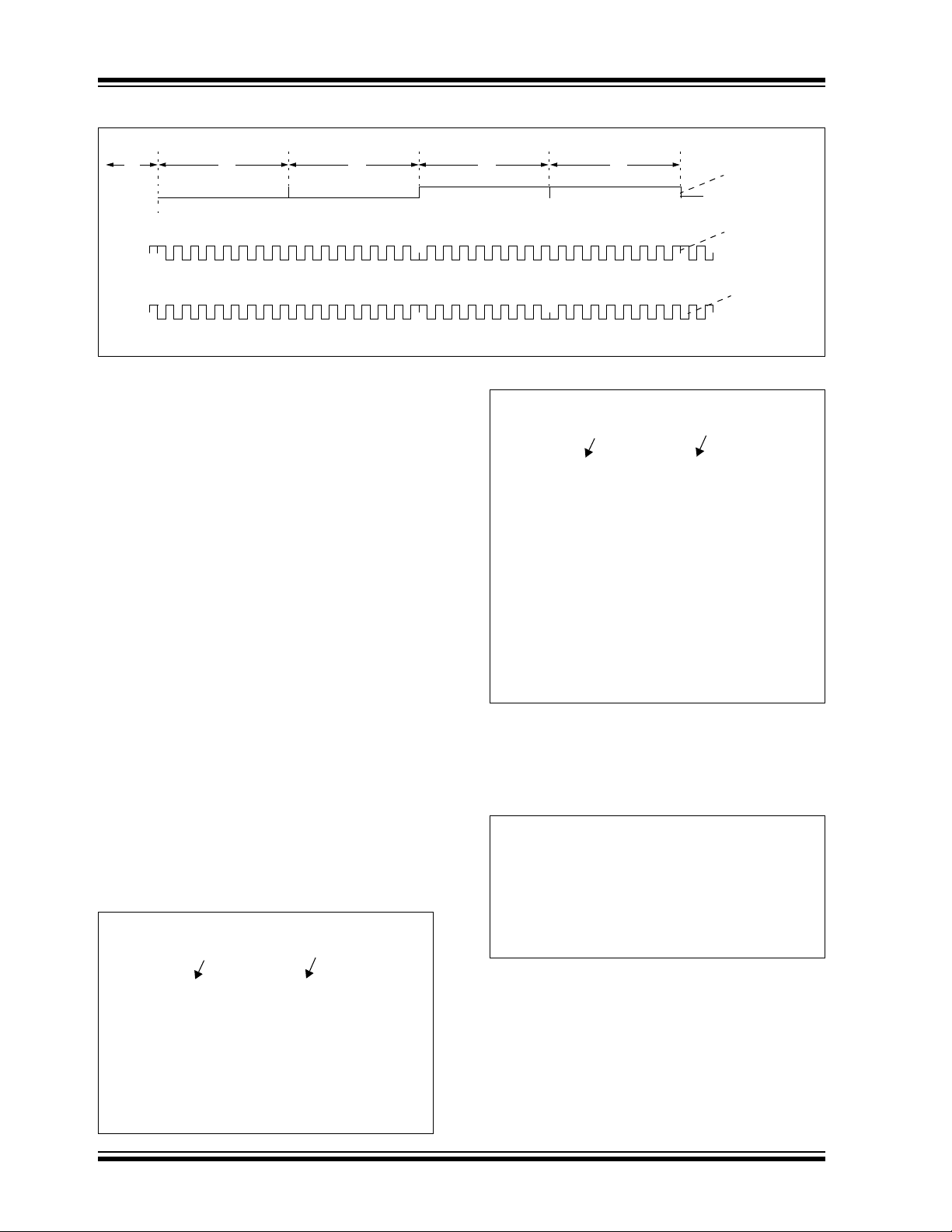
4.0 CONTACTLESS
PROGRAMMING
The contactless pr ogra mm in g of the dev ic e is poss ibl e
for blank devi ces (CB 12=0) only and is recommended
for only low-volume, ma nua l ope rati on du ring dev elo pment. In volume production, the MCRF200 is normally
used as a factory programmed device only. The
contactless programming timing sequence consists of:
a) RF power-up signal.
b) Short gap (absence of RF field).
c) Verify signal (continuous RF signal).
d) Programming signal.
e) Device response with program me d dat a .
The blank device (CB12=0) understands the RF
power-up followed by a gap as a blank checking
command, and out puts 128 bits of FSK data with all ‘ 1’s
after the short gap. To see this blank data (verify), the
reader/programmer must provide a continuous RF
signal for 128 bit-time. (The blank (unprogrammed)
device has all ‘F’s in its memory array. Therefore, the
blank data sh ould be a ll ‘ 1’s in FSK format). Since the
blank device operates at Default mode (MOD128),
there are 128 RF cycles for each bit. Therefore, the
time requirement to complete this verify is 128 bits x
128 RF cycles/bit x 8 use/cycles = 131.1 msec for
125 kHz signal.
As soon as the device c ompletes the verify, it enters the
programming mode. The reader/programmer must
provide RF programming data right after the verify. In
this programming mode, each bit lasts for 128 RF
cycles. Refer to Figure 4-1 for the contactless pro gramming sequence.
Customer must provide the following specific voltage
for the programming:
1. Power-up and verify signal = 13.5V ±1 V
2. Programming voltage:
- To program bit to ‘1’: 13.5V ±1 V
- To program bit to ‘0’: 30V ±2 VPP
After the programming cycle, the device outputs
programmed data (response). The reader/programmer
can send the programming data repeatedly after the
device response until the programming is successfully
completed. The device locks the CB12 as soon as the
programming mod e (out of field) is exited an d become s
a read-only device.
Once the device is programmed (CB12=1), the device
outputs its data according to the configuration register.
The PG103001 (Contactless Programmer) is used for
the programming of the device. The voltage level
shown in Figure 4-1 is adjusted by R5 and R7 in the
contactless programmer. Refer to the MicroID
125 kHz RFID System Design Guide (DS51115) for
more information.
PP
PP
MCRF200
™
2003 Microchip Technology Inc. DS21219H-page 9

MCRF200
FIGURE 4-1: CONTACTLESS PROGRAMMING SEQUENCE
Bit 3…
PP
Program
Verify
13.5 ± 1 VPP
(R7)
30 ± 2 V
128 bits
(R5)
∆t = Guard Band
High-power signal: programs bit = 0
1 bit = 128 cycles x 8 µs/cycle = 1.024 ms
Note: Low-power signal: leaves bit = 1
Signal
High-Power
Bit 1 Bit 2
Signal
Low-Power
FSK Signal
PP
13.5 ±1 V
~ 50 - 100 µs
Power-up Gap
Contactless Programming Protocol
f = 125 kHz
t = 8 µs
DS21219H-page 10 2003 Microchip Technology Inc.
80 - 180 µs
128 bits x 128 cycles/bit x 8 µs/cycle = 131.1 ms
0V
PP
(R5)
13.5 ± 1 V
Default programming protocol = FSK, Fc/8/10, 128 bits
For 96-bit programming, bits 33-64 are ‘don’t care’, but all
128-bit cycles must be in the sequence.

MCRF200
5.0 MECHANICAL
SPECIFICATIONS FOR DIE
AND WAFER
FIGURE 5-1: DIE PLOT
Device Test Only
VSS VCC RESET I/O
TABLE 5-1: PAD COORDINATES (µm)
Passivation
Openings
Pad
Name
V
A 90.0 90.0 427.50 -734.17
VB 90.0 90.0 -408.60 -734.17
Note 1: All coordinates are referenced fr om the
Pad
Width
center of the die.
2: Die size: 1.1215 mm x 1.7384 mm
Pad
Height
44.15 mils x 68.44 mils
Pad
Center X
Pad
Center Y
TABLE 5-2: PAD FUNCTION TABLE
Name Function
V
A Antenna Coil connection
B
V
VSS For device test only
V
CC
RESET
I/O
Do Not Connect to Antenna
VB VA
2003 Microchip Technology Inc. DS21219H-page 11

MCRF200
TABLE 5-3: DIE MECHANICAL DIMENSIONS
Specifications Min Typ Max Unit Comments
Bond pad opening —
—
Die backgrind thickness —
—
—
—
Die backgrind thicknes s tole ran ce —
—
Die passivation thick nes s (mu lti lay er) — 0.90 50 — µm Note 4
Die Size:
Die size X*Y before saw (step size)
Die size X*Y after saw
Note 1: The bond pad size is that of the passivation opening. The metal overlaps the bond pad passivation by at
least 0.1 mil.
2: Metal Pad Composition is 98.5% Aluminum with 1% Si and 0.5% Cu.
3: As the die thickness decreases, susceptibility to cracking increases. It is recommended that the die be as
thick as the application will allow.
4: The Die Passivation thickness (0.905 µm) can vary by device depending on the mask set used. The
passivation is formed by:
-Layer 1: Oxide (undoped oxide 0.135 µm)
-Layer 2: PSG (doped oxide, 0.43 µm)
-Layer 3: Oxynitride (top layer, 0.34 µm)
5: The conversion rate is 25.4 µm/mil.
——44.15 x 68.44
3.5 x 3.5
89 x 89
7
177.8
11
279.4
—
—
42.58 x 66.87——
—
—
—
—
—
—
±1
±25.4
milµmNote 1, Note 2
milµmSawed 6” wafer on frame
(option = WF) Note 3
milµmUnsawed wafer
(option = W) Note 3
mil
µm
mil
mil——
Notice: Extreme care is urged in the handling and assembly of die products since they are susceptible to
mechanical and electrostatic damage.
TABLE 5-4: WAFER MECHANICAL SPECIFICATIONS
Specifications Min Typ Max Unit Comments
Wafer Diameter — 8 — inch 150 mm
Die separation line width — 80 — µm
Dice per wafer — 14,000 — die
Batch size — 24 — wafer
DS21219H-page 12 2003 Microchip Technology Inc.

MCRF200
6.0 FAILED DIE IDENTIFICATION
Every die on the wafer is electrically tested according
to the data sheet specifications and visually inspected
to detect any mechanical damage such as mechanical
cracks and scratches.
Any failed die in th e test or visual i nspection is id entified
by black colored ink. Therefore, any die covered with
black ink should not be used.
The ink dot specification:
• Ink dot si ze: minimum 20 µm x 20 µm
• Position: central third of die
• Color: black
7.0 WAFER DELIVERY
DOCUMENTATION
Each wafer container is marked with the following
information:
• Microchip Technology Inc. MP Code
• Lot Number
• Total number of wafers in the container
• Total number of good dice in the container
• Average die per wafer (DPW)
• Scribe number of wafers with number of good
dice
8.0 NOTICE ON DIE AND WAFER
HANDLING
The device is very susceptible to Electrostatic
Discharge (ESD). ESD can cause critical damage to
the device. Special attention is needed during the
handling process.
Any untraviolet (UV) light can erase the memory cell
contents of an unpackaged device. Flourescent lights
and sun light can also erase the memory cell although
it takes more time th an UV lamp s. T herefore , keep an y
unpackaged devices out of UV light and also avoid
direct exposure from strong flourescent lights and sun
light.
Certain integrated circuit (IC) manufacturing, chip-onboard (COB) and tag a ssembly opera tions may use UV
light. Operations such as backgrind, de-tape, certain
cleaning operatio ns, epoxy or gl ue cure should be done
without exposing the die surface to UV light.
Using x-ray for die inspection will not harm the die, nor
erase memory cell contents.
2003 Microchip Technology Inc. DS21219H-page 13

MCRF200
9.0 PACKAGING INFORMATION
9.1 Package Marking Information
8-Lead PDIP (300 mil)
XXXXXXXX
XXXXXNNN
YYWW
8-Lead SOIC (150 mil)
XXXXXXXX
XXXXYYWW
NNN
Example:
MCRF200
XXXXXNNN
0025
Example:
MCRF200
XXX0025
NNN
Legend: XX...X Customer specific information*
Y Year code (last digit of calendar year)
YY Year code (last 2 digits of calendar year)
WW Week code (week of January 1 is week ‘01’)
NNN Alphanumeric traceab il ity code
Note: In the event the full Microchip p art number cann ot be mark ed on on e line, it will
be carried over to the next li ne th us l im itin g the num be r of av ail abl e ch aracters
for customer specific information.
* Standard device marking consists of Microchip part number, year code, week code, and traceability
code.
DS21219H-page 14 2003 Microchip Technology Inc.

8-Lead Plastic Dual In-line (P) – 300 mil (PDIP)
E1
D
2
MCRF200
n
E
β
eB
UNITS
Number of Pins
Pitch
Top to Seating Plane A .140 .155 .170 3.56 3.94 4.32
Molded Package Thickness A2 .115 .130 .145 2.92 3.30 3.68
Base to Seating Plane A1 .015 0.38
Shoulder to Shoulder Width E .300 .313 .325 7.62 7.94 8.26
Molded Package Width E1 .240 .250 .260 6.10 6.35 6.60
Overall Length D .360 .373 .385 9.14 9.46 9.78
Tip to Seating Plane L .125 .130 .135 3.18 3.30 3.43
Lead Thickness
Upper Lead Width B1 .045 .058 .070 1.14 1.46 1.78
Lower Lead Width B .014 .018 .022 0.36 0.46 0.56
Overall Row Spacing § eB .310 .370 .430 7.87 9.40 10.92
Mold Draft Angle Top
Mold Draft Angle Bottom
* Controlling Parameter
§ Significant Characteristic
Notes:
Dimensions D and E1 do not include mold flash or protrusions. Mold flash or protrusions shall not exceed
.010” (0.254mm) per side.
JEDEC Equivalent: MS-001
Drawing No. C04-018
DIMENSION LIMITS MIN NOM MAX MIN NOM MAX
1
α
A
c
MIN
n
p
c
α
β
.008 .012 .015 0.20 0.29 0.38
5
5
A1
B1
B
INCHES* MILLIMETERS
88
.100 2.54
10
10
15
15
5
5
A2
L
p
10
10
15
15
2003 Microchip Technology Inc. DS21219H-page 15

MCRF200
8-Lead Plastic Small Outline (SN) – Narrow, 150 mil (SOIC)
E
E1
p
D
2
B
n
1
h
45°
c
φ
β
UNITS
Number of Pins
Pitch
Foot Angle
Lead Thickness
Mold Draft Angle Top
Mold Draft Angle Bottom
* Controlling Parameter
§ Significant Characteristic
Notes:
Dimensions D and E1 do not include mold flash or protrusions. Mold flash or protrusions shall not exceed
.010” (0.254mm) per side.
JEDEC Equivalent: MS-012
Drawing No. C04-057
n
p
φ
c
α
β
L
0
0
0
A
A1
MILLIMETERSINCHES*
88
.050
.061.053AOverall Height
.056.052A2Molded Package Thickness
.007.004A1Standoff §
.237.228EOverall Width
.154.146E1Molded Package Width
.193.189DOverall Length
.015.010hChamfer Distance
.025.019LFoot Length
4
.009.008
.017.013BLead Width
12
12
8
15
15
04
1.27
1.551.35.069
1.421.32.061
.18.10.010
6.025.79.244
3.913.71.157
4.904.80.197
.38.25.020
.62.48.030
.23.20.010
.42.33.020
120
120
α
A2
MAXNOMMINMAXNOMMINDIMENSION LIMITS
1.75
1.55
.25
6.20
3.99
5.00
.51
.76
8
.25
.51
15
15
DS21219H-page 16 2003 Microchip Technology Inc.

1M/3M COB (IOA2)
MCRF200
MCRF200 COB
5mm
8mm
Antenna Coil Connection
Thickness = 0.4mm
2003 Microchip Technology Inc. DS21219H-page 17

MCRF200
NOTES:
DS21219H-page 18 2003 Microchip Technology Inc.

MCRF200
ON-LINE SUPPORT
Microchip provides on-line support on the Microchip
World Wide Web site.
The web site is used b y Mic rochip as a me ans to m ake
files and information easily available to customers. To
view the site, the use r must have access to the Intern et
and a web browser, such as Netscape
Internet Explorer. Files are also available for FTP
download from our FTP site.
Connecting to the Microchip Internet
Web Site
The Microchip web site is available at the following
URL:
www.microchip.com
The file transfer site is available by using an FTP
service to connect to:
ftp://ftp.microchip.com
The web site and file transfer site provide a variety of
services. Users may download files for the latest
Development Tools, Data Sheets, Application Notes,
User's Guides, Articles and Sample Programs. A variety of Micr ochip specific bu siness informatio n is also
available, including listings of Microchip sales offices,
distributors and factory representatives. Other data
available for consideration is:
• Latest Microchip Press Releases
• Technical Support Section with Frequently Asked
Questions
• Design Tips
• Device Errata
• Job Postings
• Microchip Consultant Program Member L isting
• Links to other useful web sites related to
Microchip Products
• Conferences for p roducts, D evelopment Systems,
technical information and more
• Listing of seminars and events
®
or Microsoft
SYSTEMS INFORMATION AND
UPGRADE HOT LINE
The Systems Information and Upgrade Line provides
system users a listing of the latest versions of all of
Microchip's development systems software products.
®
Plus, this line provides information on how customers
can receive the most c urrent upgrade kit s. The Hot Line
Numbers are:
1-800-755-2345 for U.S. and most of Canada, and
1-480-792-7302 for the rest of the world.
042003
2003 Microchip Technology Inc. DS21219H-page 19

MCRF200
READER RESPONSE
It is our intentio n to pro vi de you with the best do cumentation po ss ib le to ensure succes sfu l u se of y ou r Mic r oc hip pro duct. If you wish to provid e your c omment s on org anizatio n, clarity, subject matter , and ways i n which o ur docum entatio n
can better serve you, please FAX your comments to the Technical Publications Manager at (480) 792-4150.
Please list the following information, and use this outline to provide us with your comments about this document.
To:
RE: Reader Response
From:
Application (optional):
Would you like a reply? Y N
Device: Literature Number:
Questions:
1. What are the best features of this document?
2. How does this document meet your hardware and software development needs?
3. Do you find the organization of this document easy to follow? If not, why?
Technical Publications Manager
Name
Company
Address
City / State / ZIP / Country
Telephone: (_______) _________ - _________
Total Pages Sent ________
FAX: (______) _________ - _________
DS21219HMCRF200
4. What additions to the document do you think would enhance the structure and subject?
5. What deletions from the document could be made without affecting the overall usefulness?
6. Is there any incorrect or misleading information (what and where)?
7. How would you improve this document?
DS21219H-page 20 2003 Microchip Technology Inc.

PRODUCT IDENTIFICATION SYSTEM
To order or obtain information, e.g., on pricing or delivery, refer to the factory or the listed sales office.
PART NO. X /XX XXX
Device
Configuration/SQTP codePackageTemperature
Range
Device MCRF200 = 125 kHz Contactless Programmable MicroID™
tag, 96/128-bit
Examples:
a) MCRF200-I/W00A = 125 kHz, industrial
temperature, wafer package, contactlessly
programmable, 96 bit, FSK Fc/8 Fc/10, direct
encoded, Fc/50 data return rate tag.
b) MCRF200-I/WFQ23 = 125 kHz, industrial
temperature, wafer sawn and mounted on
frame, factory programmed.
MCRF200
Temperature Range I = -40°C to +85°C (Industrial)
Package WF = Sawed wafer on frame (7 mil backg rind)
Configuration Three-digit HEX value to be programmed into the configura-
SQTP Code An assigned custom, 3-digit code used for tracking and
W = Wafer (11 mil b ackgrind)
S = Dice in waffle pack
P = Plastic PDIP (300 mil Body) 8-lead
SN = Plastic SOIC (150 mil Body) 8-lead
1M = 0.40 mm (I0A2 package) COB Module w/1000 pF
3M = 0.40 mm (I0A2 package) COB Module with 330
tion register. Three HEX characters correspond to 12 binary
bits. These bits are programmed into the configuration
register MSB first (CB12, CB11...CB1). Refer to example.
controlling production and customer data files for factory
programming. In this case the configuration code is not
shown in the part number, but is captured in the SQTP
documentation.
capacitor
pF capacitor
The configuration register is:
CB12 CB11 CB10 CB9 CB8 CB7 CB6 CB5 CB4 CB3 CB2 CB1
0 0 0 000001010
Sales and Support
Data Sheets
Products supported by a preliminary Data Sheet may have an errata sheet describing minor operational differences and
recommended workarounds. To determine if an errata sheet exists for a particular device, please contact one of the following:
1. Your local Microchip sales office
2. The Microchip Corporate Literature Center U.S. FAX: (480) 792-7277
3. The Microchip Worldwide Site (www.microchip.com)
Please specify which device, revision of silicon and Data Sheet (include Literature #) you are using.
New Customer Notification System
Register on our web site (www.microchip.com/cn) to receive the most current information on our products.
2003 Microchip Technology Inc. DS21219H-page 21

MCRF200
NOTES:
DS21219H-page 22 2003 Microchip Technology Inc.

Note the following details of the code protection feature on Microchip devices:
• Microchip products meet the specification contained in their particular Microchip Data Sheet.
• Microchip believes that its family of products is one of the most secure families of its kind on the market today, when used in the
intended manner and under normal conditions.
• There are dishonest and possibly illegal methods used to breach the code protection feature. All of these methods, to our
knowledge, require using the Microchip products in a manner outside the operating specifications contained in Microchip's Data
Sheets. Most likely, the person doing so is engaged in theft of intellectual property.
• Microchip is willing to work with the customer who is concerned about the integrity of their code.
• Neither Microchip nor any other semiconductor manufacturer can guarantee the security of their code. Code protection does not
mean that we are guaranteeing the product as “unbreakable.”
Code protection is constantly evolving. We at Microchip are committed to continuously impro ving the cod e protection features of our
products. Attempts to break microchip’s code protection feature may be a violation of the Digital Millennium Copyright Act. If such acts
allow unauthorized access to your software or other copyrighted work, you may have a right to sue for relief under that Act.
Information contained in this publication regarding device
applications and the like is intended through suggestion only
and may be superseded by updates. It is your responsibility to
ensure that your application meets with your specifications.
No representation or warranty is given and no liability is
assumed by Microchip Technology Incorporated with respect
to the accuracy or use of such information, or infringement of
patents or other intellectual property rights arising from such
use or otherwise. Use of Microchip’s products as critical components in life support systems is not authorized except with
express written approval by Microchip. No licenses are conveyed, implicitly or otherwise, under any intellectual property
rights.
Trademarks
The Microchip name and logo, the Microchip logo, Accuron,
dsPIC, K
EELOQ, MPLAB, PIC, PICmic ro, PI C START,
PRO MATE and PowerSmart are registered trademarks of
Microchip Technology Incorporated in the U.S.A. and other
countries.
AmpLab, FilterLab, microID, MXDEV, MXLAB, PICMASTER,
SEEVAL, SmartShunt and The Embedded Control Solutions
Company are registered trademarks of Microchip Technology
Incorporated in the U.S.A.
Application Maestro, dsPICDEM, dsPICDEM.net,
dsPICworks, ECAN, ECONOMONITOR, FanSense,
FlexROM, fuzzyLAB, In-Circuit Serial Programming, ICSP,
ICEPIC, microPort, Migratable Memory, MPASM, MPLIB,
MPLINK, MPSIM, PICkit, PICDEM, PICDEM.net, PICtail,
PowerCal, PowerInfo, PowerMate, PowerTool, rfLAB, rfPIC,
Select Mode, SmartSensor, SmartTel and Total Endurance
are trademarks of Microchip Technology Incorporated in the
U.S.A. and other countries.
Serialized Quick Turn Programming (SQTP) is a service mark
of Microchip Technology Incorporated in the U.S.A.
All other trademarks mentioned herein are property of their
respective companies.
© 2003, Microchip Technology Incorporated, Printed in the
U.S.A., All Rights Reserved.
Printed on recycled paper.
Microchip re cei v ed I S O/T S - 16 949 : 20 02 qu ality system c er t if ic at io n f or
its worldwide headquarters, design and wafer fabrication facilities in
Chandler and Tempe, Arizona and Mountain View, California in October
2003 . The Company’s quality system processes and procedures are
for its PICmicro
EEPROMs, microperipherals, non-volatile memory and analog
products. In addition, Microchip’s quality system for the design and
manufacture of development systems is ISO 9001:2000 certified.
®
8-bit MCUs, KEELOQ
®
code hopping devices, Serial
2003 Microchip Technology Inc. DS21219H-page 23

WORLDWIDE SALES AND SERVICE
AMERICAS
Corporate Office
2355 West Chandler Blvd.
Chandler, AZ 85224-6199
Tel: 480-792-7200
Fax: 480-792-7277
Technical Support: 480-792-7627
Web Address: http://www.microchip.com
Atlanta
3780 Mansell Road, Suite 130
Alpharetta, GA 30022
Tel: 770-640-0034
Fax: 770-640-0307
Boston
2 Lan Drive, Suite 120
Westford, MA 01886
Tel: 978-692-3848
Fax: 978-692-3821
Chicago
333 Pierce Road, Suite 180
Itasca, IL 60143
Tel: 630-285-0071
Fax: 630-285-0075
Dallas
4570 Westgrove Drive, Suite 160
Addison, TX 75001
Tel: 972-818-7423
Fax: 972-818-2924
Detroit
Tri-Atria Office Building
32255 Northwestern Highway, Suite 190
Farmington Hills, MI 48334
Tel: 248-538-2250
Fax: 248-538-2260
Kokomo
2767 S. Albright Road
Kokomo, IN 46902
Tel: 765-864-8360
Fax: 765-864-8387
Los Angeles
18201 Von Karman, Suite 1090
Irvine, CA 92612
Tel: 949-263-1888
Fax: 949-263-1338
Phoenix
2355 West Chandler Blvd.
Chandler, AZ 85224-6199
Tel: 480-792-7966
Fax: 480-792-4338
San Jose
1300 Terra Bella Avenue
Mountain View, CA 94043
Tel: 650-215-1444
Toronto
6285 Northam Drive, Suite 108
Mississauga, Ontario L4V 1X5, Cana da
Tel: 905-673-0699
Fax: 905-673-6509
ASIA/PACIFIC
Australia
Suite 22, 41 Rawson Street
Epping 2121, NSW
Australia
Tel: 61-2-9868-6733
Fax: 61-2-9868-6755
China - Beijing
Unit 706B
Wan Tai Bei Hai Bldg.
No. 6 Chaoyangmen Bei Str.
Beijing, 100027, China
Tel: 86-10-85282100
Fax: 86-10-85282104
China - Chengdu
Rm. 2401-2402, 24th Floor,
Ming Xing Financial Tower
No. 88 TIDU Street
Chengdu 610016, China
Tel: 86-28-86766200
Fax: 86-28-86766599
China - Fuzhou
Unit 28F, World Trade Plaza
No. 71 Wusi Road
Fuzhou 350001, China
Tel: 86-591-7503506
Fax: 86-591-7503521
China - Hong Kong SAR
Unit 901-6, Tower 2, Metroplaza
223 Hing Fong Road
Kwai Fong, N.T., Hong Kong
Tel: 852-2401-1200
Fax: 852-2401-3431
China - Shanghai
Room 701, Bldg. B
Far East International Plaza
No. 317 Xian Xia Road
Shanghai, 200051
Tel: 86-21-6275-5700
Fax: 86-21-6275-5060
China - Shenzhen
Rm. 1812, 18/F, Building A, United Plaza
No. 5022 Binhe Road, Futian District
Shenzhen 518033, China
Tel: 86-755-82901380
Fax: 86-755-8295-1393
China - Shunde
Room 401, Hongjian Building
No. 2 Fengxiangnan Road, Ronggui Town
Shunde City, Guangdong 528303, China
Tel: 86-765-8395507 Fax: 86-765-8395571
China - Qingdao
Rm. B505A, Fullhope Plaza,
No. 12 Hong Kong Central Rd.
Qingdao 266071, China
Tel: 86-532-5027355 Fax: 86-532-5027205
India
Divyasree Chambers
1 Floor, Wing A (A3/A4)
No. 11, O’Shaugnessey Road
Bangalore, 560 025, India
Tel: 91-80-2290061 Fax: 91-80-2290062
Japan
Benex S-1 6F
3-18-20, Shinyokohama
Kohoku-Ku, Yokohama-shi
Kanagawa, 222-0033, Japan
Tel: 81-45-471- 6166 Fax: 81-45-4 71 -61 22
Korea
168-1, Youngbo Bldg. 3 Floor
Samsung-Dong, Kangnam-Ku
Seoul, Korea 135-882
Tel: 82-2-554-7200 Fax: 82-2-558-5932 or
82-2-558-5934
Singapore
200 Middle Road
#07-02 Prime Centre
Singapore, 188980
Tel: 65-6334-8870 Fax: 65-6334-8850
Taiwan
Kaohsiung Branch
30F - 1 No. 8
Min Chuan 2nd Road
Kaohsiung 806, Taiwan
Tel: 886-7-536-4818
Fax: 886-7-536-4803
Taiwan
Taiwan Branch
11F-3, No. 207
Tung Hua North Road
Taipei, 105, Taiwan
Tel: 886-2-2717-7175 Fax: 886-2-2545-0139
EUROPE
Austria
Durisolstrasse 2
A-4600 Wels
Austria
Tel: 43-7242-2244-399
Fax: 43-7242-2244-393
Denmark
Regus Business Centre
Lautrup hoj 1-3
Ballerup DK-2750 Denmark
Tel: 45-4420-9895 Fax: 45-4420-9910
France
Parc d’Activite du Moulin de Massy
43 Rue du Saule Trapu
Batiment A - ler Etage
91300 Massy, France
Tel: 33-1-69-53-63-20
Fax: 33-1-69-30-90-79
Germany
Steinheilstrasse 10
D-85737 Ismaning, Germany
Tel: 49-89-627-144-0
Fax: 49-89-627-144-44
Italy
Via Quasimodo, 12
20025 Legnano (MI)
Milan, Italy
Tel: 39-0331-742611
Fax: 39-0331-466781
Netherlands
P. A. De Biesbosch 14
NL-5152 SC Drunen, Netherlands
Tel: 31-416-690399
Fax: 31-416-690340
United Kingdom
505 Eskdale Road
Winnersh Triangle
Wokingham
Berkshir e, England RG41 5TU
Tel: 44-118-921-5869
Fax: 44-118-921-5820
11/24/03
DS21219H-page 24 2003 Microchip Technology Inc.
 Loading...