


MCP9800/1/2/3
r
2-Wire High-A ccuracy Temperature Sensor
Features
• Temperature-to-Digit al C onv erte r
• Accuracy with 12-bit Resolution:
- ±0.5°C (typ.) at +25°C
- ±1°C (max.) from -10°C to +85°C
- ±2°C (max.) from -10°C to +125°C
- ±3°C (max.) from -55°C to +125°C
• User-selectable Resolution: 9 – 12 bit
• Operating Voltage Range: 2.7V to 5.5V
• 2-wire Interface: I
2
C™/SMBus Compatible
• Operating Current: 200µA (typ.)
• Shutdown Current: 1µA (max.)
• Power-saving One-shot Temperature
Measurement
• Available Packages: SOT-23-5, MSOP-8, SOIC-8
Typical Applications
• Personal Computers and Servers
• Hard Disk Drives and Other PC Peripherals
• Entertainment Systems
• Office Equipment
• Data Communication Equipment
• Mobile Phones
• General-purpose Temperature Monitoring
Description
Microchip Technology Inc.’s MCP9800/1/2/3 family of
digital temperature sensors converts temperatures
between -55°C and +125°C to a digital word. They
provide an accuracy of ±1°C (max.) from -10°C to
+85°C.
The MCP9800/1/2/3 family comes with user-programmable registers that provide flexibility for temperature
sensing applications. The register settings allow userselectable 9-bit to 12-bit temperature measurement
resolution, configur ation of the power-savi ng Shutdown
and One-shot (single conversion on command while in
the Shutdown) modes and the specification of both
temperature alert output and hysteresis limits. When
the temperature changes beyond the specified limits,
the MCP9800/1/2/3 outputs an alert signal. The user
has the option of setting the alert output signal polarity
as an active-low or active-high comparator output for
thermostat operati on, or as t emperature event interru pt
output for microprocessor-based systems.
2
This sensor has an industry standard 2-wire, I
C™/
SMBus compatible serial interface, allowing up to eight
devices to be controlled in a single serial bus. Th ese features make the MCP9800/1/2/3 ideal for sophisticated
multi-zone temperature-monitoring applications.
Package Types
Typical Application
MCP9800/02
V
DD
GND
ALERT
1
2
3
5
4
R
SDA
SCLK
R
PULL-UP
V
DD
PICmicro
®
Microcontrolle
PIC16F737
I
2
C™ Port
I/O Port
MCP9800
MCP9802
SOT-23-5
V
1
DD
GND
2
ALERT
3
MCP9800/02A0: A2, A1, A0 are internally set to (0, 0, 0)
MCP9800/02A5: A2, A1, A0 are internally set to (1, 0, 1)
MCP9802/03: Serial Bus time-out 35 ms (typ.)
5
4
SDA
SCLK
ALERT
SOIC, MSOP
SDA
SCLK
GND
MCP9801
MCP9803
1
2
3
4
V
8
DD
A0
7
A1
6
A2
5
2004 Microchip Technology Inc. DS21909B-page 1
MCP9800/1/2/3
1.0 ELECTRICAL CHARACTERISTICS
Absolute Maximum Ratings †
VDD....................................................................... 6.0V
Volt a ge at all Inpu t/O utp ut pins.... GND – 0.3V to 5.5V
Storage temperature ..........................-65°C to +150°C
Ambient temp. with power applied .....-55°C to +125°C
Junction Temperature (T
ESD protection on all pins (HBM:MM)....... (4 kV:400V)
)..................................150°C
J
PIN FUNCTION TABLE
NAME FUNCTION
SDA Bidirectional Serial Data (open-drain
SCLK Serial Clock Input
ALERT Temperature Alert Output (open-drain)
A2 Address Select Pin (bit 2)
A1 Address Select Pin (bit 1)
A0 Address Select Pin (bit 0)
V
GND Ground
output)
Power Supply Input
DD
Latch-Up Current at each pin........................ ±200 mA
†Notice: Stresses above those listed under “Maximum
ratings” may cause permanent damage to the device. This is
a stress rating only and functional operation of the device at
those or any other conditions above those indicated in the
operational listings of this specification is not implied.
Exposure to maximum rating conditions for extended periods
may affect device reliability.
DC CHARACTERISTICS
Electrical Specifications: Unless otherwise indicated, VDD = 2.7V to 5.5V, GND = Ground, and
T
= -55°C to +125°C.
A
Parameters Sym Min Typ Max Unit Conditions
Power Supply
Operating Voltage Range V
Operating Current I
Shutdown Current I
Power On Reset Threshold (POR) V
Temperature Sensor Accuracy
Accuracy with 12-bit Resolution:
T
= +25°C T
A
-10°C < T
-10°C < T
-55°C < T
≤ +85°C T
A
≤ +125°C T
A
≤ +125°C T
A
Internal Σ∆ ADC
Conversion Time:
9-bit Resolution t
10-bit Reso lution t
1 1-bit Resolution t
12-bit Reso lution t
Alert Output (Open-drain)
High-level Current I
Low-level Voltage V
Thermal Response
Response Time t
DD
DD
SHDN
POR
ACY
ACY
ACY
ACY
CONV
CONV
CONV
CONV
OH
OL
RES
2.7 — 5.5 V
— 200 400 µA Continuous Operation
— 0.1 1 µ A Shutdown Mode
—1.7— VVDD falling edge
— ±0.5 — °C VDD = 3.3V
-1.0 — +1.0 °C VDD = 3.3V
-2.0 — +2.0 °C VDD = 3.3V
-3.0 — +3.0 °C VDD = 3.3V
— 30 75 ms 33 samples/sec (typ.)
— 60 150 ms 17 samples/sec (typ.)
— 120 300 ms 8 samples/sec (typ.)
— 240 600 ms 4 samples/sec (typ.)
——1µAV
——0.4VI
OH
= 3 mA
OL
— 1.4 — s Time to 63% (88°C)
27°C (Air) to 125°C (oil bath)
= 5V
DS21909B-page 2 2004 Microchip Technology Inc.
MCP9800/1/2/3
DIGITAL INPUT/OUTPUT PIN CHARACTERISTICS
Electrical Specifications: Unless otherwise indicated, VDD = 2.7V to 5.5V, GND = Ground and
T
= -55°C to +125°C.
A
Parameters Sym Min Typ Max Units Conditions
Serial Input/Output (SCLK, SDA, A0, A1, A2)
Input
High-level Voltage V
Low-level Voltage V
Input Current I
Output (SDA)
Low-level Voltage V
High-level Current I
Low-level Current I
Capacitance C
SDA and SCLK Inputs
Hysteresis V
IH
IL
IN
OL
OH
OL
IN
HYST
0.7 V
——0.3VDDV
-1 — +1 µA
——0.4VIOL= 3 mA
——1µAV
6——mAV
—10—pF
0.05 V
—— V
DD
—— V
DD
OH
= 0.6V
OL
= 5V
Graphical Symbol Description
INPUT OUTPUT
Voltage
V
Current
I
DD
IN
V
IH
V
IL
time
time
Voltage
V
DD
V
OL
Current
I
OL
I
OH
time
time
TEMPERATURE CHARACTERISTICS
Electrical Specifications: Unless otherwise indicated, VDD= +2.7V to +5.5V, GND = Ground.
Parameters Sym Min Typ Max Units Conditions
Temperature Ranges
Specified Temperature Range T
Operating Temperature Range T
Storage Temperature Range T
A
A
A
Thermal Package Resistances
Thermal Resistance, 5L-SOT23 θ
Thermal Resistance, 8L-SOIC θ
Thermal Resistance, 8L-MSOP θ
JA
JA
JA
Note 1: Operation in this range must not cause T
-55 — +125 °C (Note 1)
-55 — +125 °C
-65 — +150 °C
—256—°C/W
—163—°C/W
—206—°C/W
to exceed Maximum Junction Temperature (+150°C).
J
2004 Microchip Technology Inc. DS21909B-page 3
MCP9800/1/2/3
SERIAL INTERFACE TIMING SPECIFICATIONS
Electrical Specifications: Unless otherwise indicated, VDD = 2.7V to 5.5V, GND = Ground, -55°C < TA < +125°C,
C
= 80 pF, and all limits measured to 50% point.
L
Parameters Sym M in Typ Max Units Conditions
2-Wire I
Serial Port Frequency f
Clock Period t
Low Clock t
High Clock t
Rise Time t
Fall Time t
Data Setup Before SCLK High t
Data Hold After SCLK Low t
Start Condition Setup Time t
Start Condition Hold Time t
Stop Condition Setup Time t
Bus Idle t
Time Out t
Timing Diagram
2
C/SMBus Compatible Interface
SU-DATA
H-DATA
SU-START
H-START
SU-STOP
START Condition
t
SU-START
SC
f
SC
SC
LOW
HIGH
R
F
IDLE
OUT
0 — 400 kHz I2C MCP9800/01
10 — 400 kHz SMBus MCP9802/03
2.5 — — µs
1.3 — — µs
0.6 — — µs
20 — 300 ns 10% to 90% of VDD (SCLK, SDA)
20 — 300 ns 90% to 10% of VDD (SCLK, SDA)
0.1 — — µs
0—0.9µs
0.6 — — µs
0.6 — — µs
0.6 — — µs
1.3 — — µs
25 35 50 ms MCP9802/03 only
t
H-START
SCLK
SDA
Data T ransmission
SCLK
SDA
STOP Condition
SCLK
SDA
t
SU-DA TA
t
H-DATA
t
HIGH
t
OUT
t
LOW
tR,t
F
t
SC
t
SU-STOP
DS21909B-page 4 2004 Microchip Technology Inc.
t
IDLE
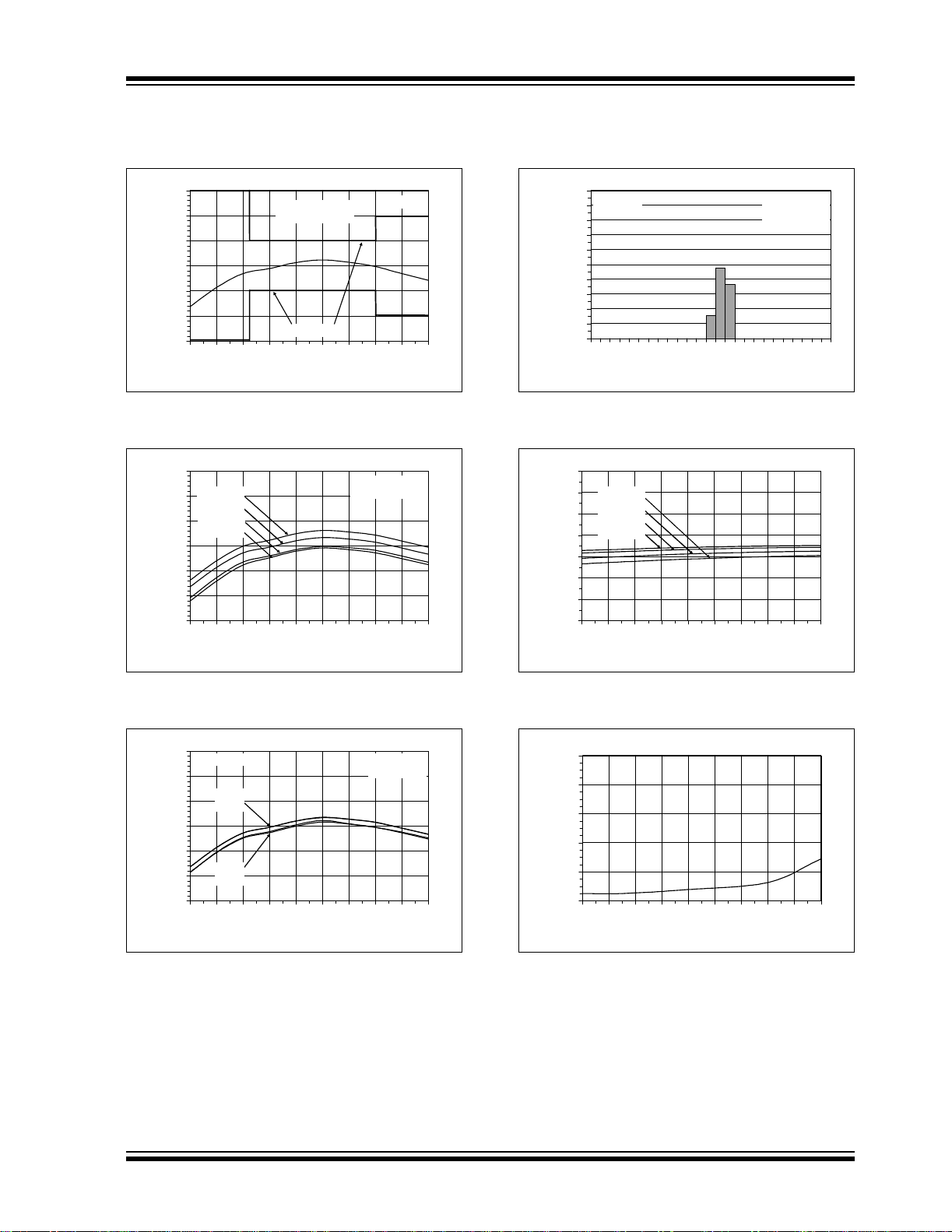
2.0 TYPICAL PERFORMANCE CURVES
Note: Unless otherwise noted: VDD = 2.7V to 5.5V.
MCP9800/1/2/3
3.0
2.0
1.0
0.0
-1.0
-2.0
Temperature Accuracy (°C)
-3.0
-55 -35 -15 5 25 45 65 85 105 125
12-Bit Resolution
160 Samples
Spec. Limits
(°C)
T
A
VDD= 3.3V
FIGURE 2-1: Average Temperature
Accuracy vs. Ambient Temperature, V
3.0
VDD = 2.7V
2.0
VDD = 3.3V
VDD = 5.0V
1.0
VDD = 5.5V
0.0
-1.0
-2.0
Temperature Accuracy (°C)
-3.0
-55 -35 -15 5 25 45 65 85 105 125
T
A
(°C)
12-Bit Resolution
160 Samples
= 3.3V.
DD
100%
90%
80%
70%
60%
50%
40%
30%
Occurrences
20%
10%
0%
TA = +25°C
= 3.3V
V
DD
-3.0
-2.5
-2.0
-1.5
-1.0
Temperature Accuracy (°C)
0.0
-0.5
0.5
1.0
5 lots
32 Samples/lot
160 Samples
1.5
2.0
FIGURE 2-4: Temperature Accuracy
Histogram, T
400
350
300
250
(µA)
200
DD
I
150
100
50
= +25°C.
A
VDD = 2.7V
VDD = 3.3V
VDD = 5.0V
VDD = 5.5V
-55 -35 -15 5 25 45 65 85 105 125
T
(°C)
A
2.5
3.0
FIGURE 2-2: Average Temperature Accuracy vs. Ambient Temperature.
3.0
Resolution
2.0
1.0
0.0
-1.0
-2.0
Temperature Accuracy (°C)
-3.0
11-Bit
12-Bit
9-Bit
10-Bit
-55 -35 -15 5 25 45 65 85 105 125
T
(°C)
A
VDD = 3.3V
160 Samples
FIGURE 2-3: Average Temperature
Accuracy vs. Ambient Temperature, V
= 3.3V.
DD
FIGURE 2-5: Supply Current vs. Ambient Temperature.
1
0.8
0.6
(µA)
0.4
SHDN
I
0.2
0
-55 -35 -15 5 25 45 65 85 105 125
(°C )
T
A
FIGURE 2-6: Shutdown Current vs. Ambient Temperatu re.
2004 Microchip Technology Inc. DS21909B-page 5

MCP9800/1/2/3
= 0.6V
= 3mA
Note: Unless otherwise noted: VDD = 2.7V to 5.5V.
48
V
OL
42
(mA)
36
OL
30
VDD = 5.5V
= 3.3V
V
DD
= 2.7V
V
DD
24
18
12
ALERT & SDA I
6
-55 -35 -15 5 25 45 65 85 105 125
(°C)
T
A
FIGURE 2-7: ALERT and SDA IOL vs. Ambient Temperature.
0.4
I
OL
(V)
0.3
OL
0.2
0.1
ALERT & SDA V
0
-55 -35 -15 5 25 45 65 85 105 125
T
(°C)
A
VDD = 5.5V
= 3.3V
V
DD
= 2.7V
V
DD
145
Average of 10 samples per package
125
105
85
65
45
Temperature Data (°C)
25
5
-202468101214161820
SOIC
MSOP
SOT-23
27°C (Air) to 125°C (Oil bath)
Time (s)
FIGURE 2-9: MCP980X Thermal Response vs Time.
FIGURE 2-8: ALERT and SDA Output
V
vs. Ambient Temperature.
OL
DS21909B-page 6 2004 Microchip Technology Inc.
3.0 PIN DESCRIPTION
The descriptions of the pins are listed in Table 3-1.
TABLE 3-1: PIN FUNCTION TABLE
MCP9800/1/2/3
MCP9800
MCP9802
SOT-23-5
5 1 SDA Bidirectional Serial Data
4 2 SCLK Serial Clock Input
3 3 ALERT T e mp erature Alert Output
2 4 GND Ground
— 5 A2 Address Select Pin (bit 2)
— 6 A1 Address Select Pin (bit 1)
— 7 A0 Address Select Pin (bit 0)
18V
MCP9801
MCP9803
MSOP, SOIC
Symbol Function
DD
3.1 Serial Data Pin (SDA)
The SDA is a bidirectional input/output pin, used to
serially transmit data to and from the host controller.
This pin requires a pull-up resistor to output data.
3.2 Serial Clock Pin (SCLK)
The SCLK is a clock input pin. All communication and
timing is relative to the signal on this pin. The clock is
generated by the host controller on the bus.
3.3 Power Supply Input (VDD)
The VDD pin is the power pin. The operating vol tage, a s
specified in the DC electrical specification table, is
applied on this pin.
3.4 Ground (GND)
The GND pin is the system ground pin.
Power Supply Input
3.5 ALERT Output
The MCP9800/1/2/3’s ALERT pin is an open-drain
output pin. The device out put s an alert signal when th e
ambient temperature goes beyond the userprogrammed temperature limit.
3.6 Address Pins (A2, A1, A0)
These pins are device or slave address input pins and
are available only with the MCP9801/03. The device
addresses for the MCP9800/02 are factory-set.
The address pins are the Leas t Significant bi ts (LSb) of
the device address bits. The Most Significant bits
(MSb) (A6, A5, A4, A3) are factory-set to <1001>. This
is illustrated in Table 3-2.
TABLE 3-2: SLAVE ADDRESS
Device A6 A5 A4 A3 A2 A1 A0
MCP9800/02A0 1001000
MCP9800/02A5 1001101
MCP9801/03 1001XXX
Note: User-selectable address is shown by X.
2004 Microchip Technology Inc. DS21909B-page 7

MCP9800/1/2/3
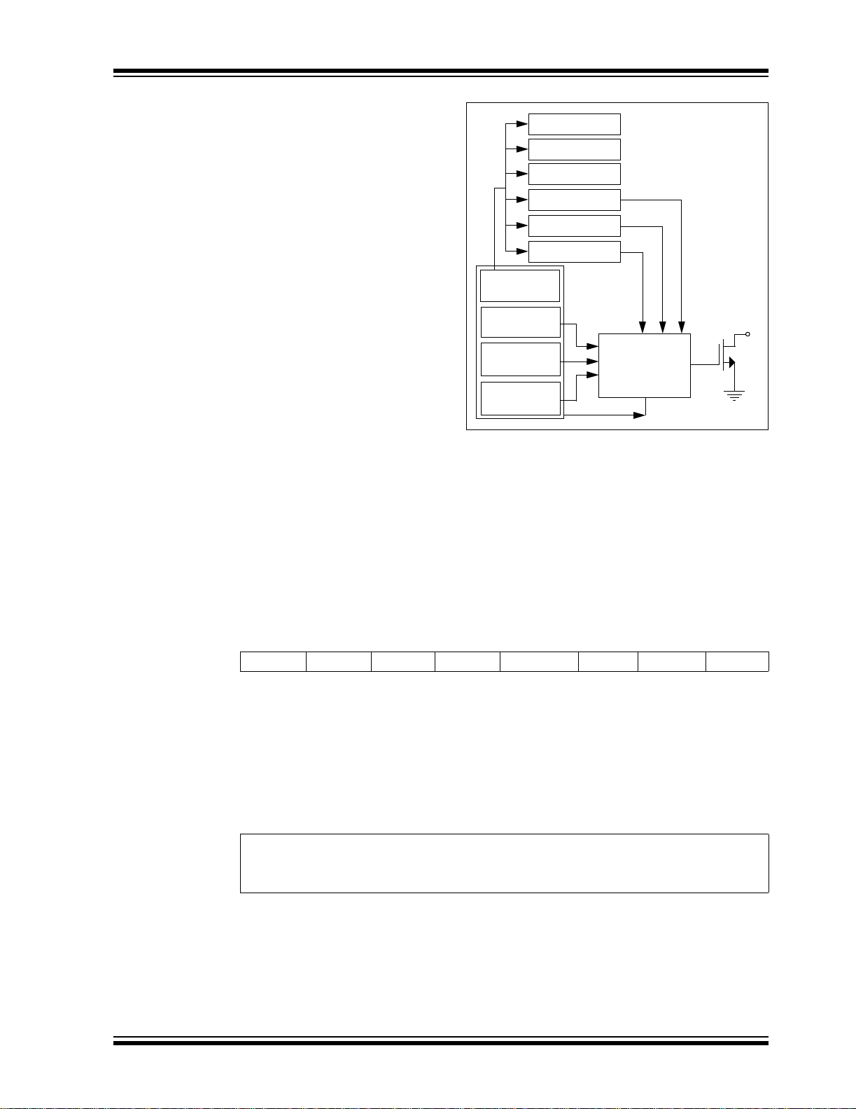
4.0 FUNCTIONAL DESCRIPTION
The MCP9800/1/2/3 family of temperature sensors
consists of a band-gap type temperature sensor, a Σ∆
Analog-to-Digital Converter (ADC), user-programmable
registers and a 2-wire I
serial interface.
Configuration
Register
Temperature
Register
T
Register
T
Register
Register
Pointer
FIGURE 4-1: Functional Block Diagram.
2
C/SMBus protocol compatible
Resolution
One-Shot
Shutdown
Fault Queue
Alert Polarity
Alert Comp/Int
HYST
SET
9-Bit
10-Bit
11-Bit
12-Bit
Σ∆ ADC
Band-Gap
Temperature
Sensor
I2C™/SMBus
Interface
4.1 Temperature Sensor
The MCP9800/1/2/3 uses the difference in the baseemitter voltag e of a transistor while its collector current
is changed from IC
depends only on the ratio of the two currents and the
ambient temperature, as shown in Equation 4-1.
to IC2. With this method, the ∆V
1
BE
EQUATION 4-1:
kT
----- -
∆
V
BE
Where:
T = temperature in kelvin
= change in diode base-emitter
∆V
BE
voltage
k = Boltzmann's constant
q = electron charge
IC1 and IC2= currents with n:1 ratio
q
ln IC
⁄()×=
1IC2
4.2 Σ∆ Analog-to-Digital Converter
A sigma-delta analog-to-digital converter is used to
convert ∆V
transistor temperature. The converter has an
adjustable resolution from 9-bits (at 30 ms conversion
time) to 12 -bits (at 240 ms conver sion time). Thus , it
allows the user to make trade-offs between resolution
and conversion time. Refer to Section 4.3.4 “Sensor
Configuration Register (CONFIG)” and
Section 4.3.4.7 “Σ∆ ADC Resolution” for details.
to a digital word that corresponds to the
BE
DS21909B-page 8 2004 Microchip Technology Inc.
4.3 Registers
The MCP9800/1/2/3 family has four registers that are
user-accessible. These registers are specified as the
ambient temperature register, the tem pera ture limit-set
register , the temperature h ysteresis regist er and device
configuration registers.
The ambient temperature register is a read-only
register and is used to acce ss the ambient tem perature
data. The dat a from th e ADC is loade d in p arall el in th e
register. The temperature limit-set and temperature
hysteresis registers are read/write registers that
provide user-programmable temperature limits. If the
ambient temperature drifts beyond the programmed
limits, the MCP9 800 /1/2 /3 outputs an alert sig nal u sin g
the ALERT pin (refer to Section 4.3.4.3 “ALERT Out-
put Configuration”). The device configurat ion register
provides access for the user to configure the
MCP9800/1/2/3’ s various features. Th ese regist ers are
described in further detail in the following sections.
MCP9800/1/2/3
Resolution
One-Shot
Shutdown
Fault Queue
Alert Polarity
Alert Comp/Int
Configuration
Register
Temperature
Register
T
HYST
Register
T
SET
Register
ALERT Output
Control Logic
FIGURE 1: Register Block Diagram.
The registers are ac ce ss ed by se ndi ng register pointer
to the MCP9800/1/2/3 usin g the serial inte rface. This is
an 8-bit pointer. However , the t wo L east Si gnifi cant bits
(LSb) are used a s poi nters an d all other bit s n eed to be
cleared <0>. This device has additional registers that
are reserved for test and calibration. If these registers
are accessed, the device may not perform accordi ng to
the specification. The pointer description is shown
below.
ALERT
Output
REGISTER 4-1: REGISTER POINTER
U-0 U-0 U-0 U-0 U-0 U-0 R/W-0 R/W-0
0 0 0 0 0 0 P1 P0
bit 7 bit 0
bit 7-3 Unimplemented: Read as ‘0’
bit 2-0 Pointer bits
00 = Temperature Register
01 = Configuration Register
10 = Temperature Hysteresis Register
11 = Temperature Limit-set Register
Legend:
R = Readable bit W = Writable bit U = Unimplemented bit, read as ‘0’
- n = Value at POR ‘1’ = Bit is set ‘0’ = Bit is cleared x = Bit is unknown
2004 Microchip Technology Inc. DS21909B-page 9

MCP9800/1/2/3
,
4.3.1 AMB IENT TEMPERATURE
REGISTER (T
The MCP9800/1/2/3 has a 16-bit read-only ambient
temperature register
temperature data. This data is formatted in two’s
complement. The bit assignments, as well as the
corresponding resolution, is shown in the register
assignment below.
The refresh rate of this register depends on the
selected ADC re soluti on. It ta kes 30 ms (ty p.) for 9 -bit
data and 240 ms (typ.) for 12-bit data. Since this
register is double-buffered, the user can read the
register while the MCP9800/1/2/3 performs analog-to-
REGISTER 4-2: AMBIENT TEMPERATURE REGISTER (TA)
)
A
(TA) that contains 9-bit to 12-bit
digital conve rsion in the ba ckground. The decimal cod e
to ambient temperature conversion is shown in
Equation 4-2:
EQUATION 4-2:
TACode 2n×=
Where:
n = -1, -2, -3 and -4 for 9-bi t, 1 0-bit, 11-bit
and 12-bit resolution, respectively
TA= Ambient Temperature (°C)
Code= MCP980 X output in deci mal
(Table 4-1)
Upper Half:
R-0 R-0 R-0 R-0 R-0 R-0 R-0 R-0
Sign 26 °C/bit 25 °C/bit 24 °C/bit 23 °C/bit 22 °C/bit 21 °C/bit 20 °C/bit
bit 15 bit 8
Lower Half:
R-0 R-0 R-0 R-0 R-0 R-0 R-0 R-0
-1
°C/bit 2
2
-2
°C/bit 2
-3
°C/bit 2
-4
°C/bit 0 0 0 0
bit 7 bit 0
Note: When the 9-bit, 10-bit or 11-bit resolutions are selected, bit 6, bit 7 or bit 8 will remain clear <0>
respectively.
Legend:
R = Readable bit W = Writable bit U = Unimplemented bit, read as ‘0’
- n = Value at POR ‘1’ = Bit is set ‘0’ = Bit is cleared x = Bit is unknown
TABLE 4-1: AMBIENT TEMPERATURE TO CODE CONVERSION
Ambient Temperature Code
9-Bit 10-Bit 11-Bit 12-Bit Binary Hexadecimal Decimal
+125°C 0111 1101 0uuu uuuu
+25.4375°C 0001 1001 0uuu uuuu 032 50 +25
+0.5°C 0000 0000 1uuu uuuu 001 1 +0.5
+125°C 0111 1101 00uu uuuu 1F4 500 +125
+25.4375°C 0001 1001 01uu uuuu 065 101 +25.25
+0.25°C 0000 0000 01uu uuuu 001 1 +0.25
+125°C 0111 1101 000u uuuu 3E8 1000 +125
+25.4375°C 0001 1001 011u uuuu 0CB 203 +25.375
+0.125°C 0000 0000 001u uuuu 001 1 +0.125
+125°C 0111 1101 0000 uuuu 7D0 2000 +125
+25.4375°C 0001 1001 0111 uuuu 197 407 +25.4375
+0.0625°C 0000 0000 0001 uuuu 001 1 +0.0625
0°C 0000 0000 0000 uuuu 000 0 0
–0.0625°C 1111 1111 1111 uuuu
–25.4375°C 1110 0110 1001 uuuu 197 -407 -25.4375
–55°C 1100 1001 0000 uuuu 370 -880 -55
Note 1: ‘u’ represents unused bits. The MCP9800/1/2/3 clears <0> the unused bits.
2: This data is in two’s complement format, which indicates ambient temperature below 0°C.
3: Negative temperature magnitude in Hexadecimal. This conversion is done by complimenting each binary bit and
adding 1.
(1)
(2)
0FA 250 +125
(3)
001
-1 -0.0625
T
(°C)
A
DS21909B-page 10 2004 Microchip Technology Inc.

MCP9800/1/2/3
4.3.2 TEMPERATURE LIMIT-SET
REGISTER (T
The MCP9800/1/2/3 has a 16-bit read/write Temperature Limit-Set register (T
in two’s compliment format. This data represents a
maximum temperature l im it. I f t he ambient temperature
exceeds this specif ied limit, the MCP9800 /1/2/3 assert s
an alert output. (Refer to Section 4.3.4.3 “ALERT Out-
put Configuration”).
This register uses the nine Most Significant bits (MSb)
and all other bits are don’t cares.
The power-up default value of T
<0 1010 0000> in binary.
REGISTER 4-3: TEMPERATURE LIMIT-SET REGISTER (T
Upper Half:
R/W-0 R/W-0 R/W-0 R/W-0 R/W-0 R/W-0 R/W-0 R/W-0
Sign 2
bit 15 bit 8
SET
6
°C/bit 25 °C/bit 24 °C/bit 23 °C/bit 22 °C/bit 21 °C/bit 20 °C/bit
)
SET
) which contains a 9-bit data
register is 80°C
SET
SET
)
Lower Half:
R/W-0 R-0 R-0 R-0 R-0 R-0 R-0 R-0
-1
°C/bit 0 0 0 0 0 0 0
2
bit 7 bit 0
Legend:
R = Readable bit W = Writable bit U = Unimplemented bit, read as ‘0’
- n = Value at POR ‘1’ = Bit is set ‘0’ = Bit is cleared x = Bit is unknown
2004 Microchip Technology Inc. DS21909B-page 11

MCP9800/1/2/3
0
4.3.3 TEMPERATURE HYSTERESIS
REGISTER (T
The MCP9800/1/2/3 has a 16-bit read/write temperature hysteresis register (T
data in two’s compliment format. This register is used
to set a hysteresis fo r the T
represents a mini mum t empera ture limi t. If the ambie nt
temperature drifts below the specified limit, the
MCP9800/1/2/3 asserts an alert output (refer to
Section 4.3.4.3 “ALERT Output Configuration”).
This register uses the nine Most Significant bits (MSb)
and all other bits are don’t cares.
The power-up default value of T
<0 1001 0110> in binary.
REGISTER 4-4: TEMPERATURE HYSTERESIS REGISTER (T
Upper Half:
R/W-0 R/W-0 R/W-0 R/W-0 R/W-0 R/W-0 R/W-0 R/W-0
Sign 2
bit 15 bit 8
6
°C/bit 25 °C/bit 24 °C/bit 23 °C/bit 22 °C/bit 21 °C/bit 20 °C/bit
)
HYST
) that contains a 9-bit
HYST
limit. Therefore, the data
SET
register is 75°C
HYST
HYST
)
Lower Half:
R/W-0 R-0 R-0 R-0 R-0 R-0 R-0 R-0
-1
2
°C/bit 0 0 0 0 0 0 0
bit 7 bit
Legend:
R = Readable bit W = Writable bit U = Unimplemented bit, read as ‘0’
- n = Value at POR ‘1’ = Bit is set ‘0’ = Bit is cleared x = Bit is unknown
DS21909B-page 12 2004 Microchip Technology Inc.

4.3.4 SENSOR CONFIGURATION
REGISTER (CONFIG)
The MCP9800/1/2/3 has an 8-bit read/write configuration register (CONFIG ) that allows the us er to select the
different features. These features include shutdown,
ALERT output s elect as comp arato r or i nterrupt outpu t,
ALERT output polarity, fault queue cycle, temperature
measurement resolution and One-shot mode (single
conversion while in shutdown). These functions are
described in detail in the following sections.
REGISTER 4-5: CONFIGURATION REGISTER (CONFIG)
R/W-0 R/W-0 R/W-0 R/W-0 R/W-0 R/W-0 R/W-0 R/W-0
One-Shot Resolution Fault Queue ALERT
bit 7 bit 0
bit 7 ONE-SHOT bit
1 = Enabled
0 = Disabled (Power-up default)
bit 5-6 Σ∆ ADC RESOLUTION bit
00 = 9 bit (Power-up default)
01 = 10 bit
10 = 11 bit
11 = 12 bit
bit 3-4 FAULT QUEUE bit
00 = 1 (Power-up default)
01 =2
10 =4
11 =6
bit 2 ALERT POLARITY bit
1 =Active-High
0 = Active-Low (Power-up default)
bit 1 COMP/INT bit
1 = Interrupt Mode
0 = Comparator Mode (Power-up default)
bit 0 SHUTDOWN bit
1 = Enable
0 = Disable (Pow er-up default)
MCP9800/1/2/3
Polarity
COMP/
INT
Shutdown
Legend:
R = Readable bit W = Writable bit U = Unimplemented bit, read as ‘0’
- n = Value at POR ‘1’ = Bit is set ‘0’ = Bit is cleared x = Bit is unknown
2004 Microchip Technology Inc. DS21909B-page 13

MCP9800/1/2/3
4.3.4.1 Shutdown Mode
The Shutdown mode disables all power-consuming
activities (including temperature sampling operations)
while leaving the serial interface active. The device
consumes 1 µA (max.) in this mode. It remains in this
mode until the configuration register is updated to
enable continuous conversion or until power is
recycled.
, T
In Shutdown mode, the CONFIG, T
A
SET
and T
HYST
registers can be read or written. However, the serial
bus activity will increase the shutdown current.
4.3.4.2 One-Shot Mode
The MCP9800/1/2/3 can also be used in a One-shot
mode that can b e select ed using bit 7 of the CONFIG
register . The One-s hot mode perf orms a single te mperature measurement and returns to Shutdown mode.
This mode is especially useful for low-power applications where temperature is measured upon command
from a controller. For example, a 9-bit T
in One-shot
A
mode consumes 200 µA (typ.) for 30 m s and 0.1 µA
(typ.) during shutdown.
To access this feature, the device needs to initially be
in Shutdown mode. This is done by sending a byte to
the CONFIG register with bit 0 set <1> and bit 7
cleared <0>. Once the device is in Shutdown mode,
CONFIG needs to be written again with bit 0 and bit 7
set <1>. This begins the single conversion cycle of
30 ms for 9-bit data. Once the conversion is
completed, T
is updated and bit 7 of CONFIG
A
becomes cleared <0> by the MCP9800/1/2/3.
TABLE 4-6: SHUTDOWN AND ONE-SHOT
MODE DESCRIPTION
Operational Mode
One-Shot
(Bit 7)
Continuous Convers ion 00
Shutdown 01
Continuous Convers ion
10
(One-shot is ignored)
One-Shot 11
Note: The shutdown command <01> needs to
be programmed before sending a oneshot command <11>.
Shutdown
(Bit 0)
4.3.4.3 ALERT Output Configuration
The ALERT output can be configured as either a
comparator output or as Interrupt Output mode using
bit 1 of CONFIG. The polarity can also be specified as
an active-high or active-low, using bit 2 of CONFIG.
The following sections describe each Output mode
and Figure 4-2 shows graphical description.
4.3.4.4 Comparator Mode
In the Comparator mode, the ALERT ou tput is asserted
when T
until T
is greater than T
A
is lower than T
A
. The pin remains active
SET
. The Comparator mode is
HYST
useful for thermostat-type applications such as turning
on a cooling fan or trig geri ng a system shutdown when
the temperature exceeds a safe operating range.
In the Comparator mode, if the device enters the
Shutdown mode with asserted ALERT output, the
output remains active during shutdown. The device
must be operating in continuous conversion, with T
below T
, for the ALERT output to be deasserted.
HYST
4.3.4.5 Interrupt Mode
In the Interrupt mode, the ALERT output is asserted
when T
deasserted when the user performs a read from any
register . This mode is designed for interrupt driv en microcontroller based systems. The microcontroller receiving
the interrupt will have to acknowledge the interrupt by
reading any register from the MCP9800/1/2/3. This will
clear the interrupt and the ALERT pin will become
deasserted. When T
1/2/3 outputs a nother i nterrupt and the co ntrolle r needs
to read a register t o deassert th e ALER T output. Sh utting
down the devic e will also r eset or deasser t the ALERT
output.
is greater than T
A
T
SET
T
A
T
HYST
ALERT
Comparator Mode
Active-Low
. However, the output is
SET
drifts below T
A
, the MCP9800/
HYST
A
ALERT
Interrupt Mode
Active-Low
FIGURE 4-2: Alert Output.
DS21909B-page 14 2004 Microchip Technology Inc.

MCP9800/1/2/3
4.3.4.6 Fault Queue
The fault queue feature can be us ed as a filter to lessen
the probability of spurious activation of the ALERT pin.
must remain above T
T
A
for the consecutive num-
SET
ber of conversion cycles selected using the Fault
Queue bits. Bit 3 and bit 4 of CONFIG can be used to
select up to six fault queue cycles. For example, if six
fault queues are selected, TA must be greater than
for six consecutive conversions before ALERT is
T
SET
asserted as a comparator or an interrupt output.
This queue setting also applies for T
remain below T
for six consecutive conversions
HYST
HYST
. TA must
before ALERT is deasserted (comparator mode) or
before another interrupt is asserted (interrupt mode).
4.3.4.7 Σ∆ ADC Resolution
The MCP9800/1/2/3 p rovides access to se lect the ADC
resolution from 9-bi t to 12-bit usi ng bit 6 and bi t 5 of the
CONFIG register. The user can gain better insight into
the trends and characteristics of the ambient
temperature by using a finer resolution. Increasing the
resolution also reduces the quantization error.
Figure 2-4 shows accuracy versus resolution.
Table 4-1 shows the T
corresponding resolution.
register conversion time for the
A
4.4 Summary of Power-up Default
The MCP9800/1/2/3 has an internal Power-on Reset
(POR) circuit. If the power supply voltage V
down to the 1.7V (typ.) thre shold , the devi ce rese t s the
registers to the power-up default settings.
Table 4-2 shows the power-up default summary.
TABLE 4-2: POWER-UP DEFAULTS
Register
T
A
T
SET
T
HYST
Pointer 00 Temperature register
CONFIG 00
Data
(Hex)
Power-up Defaults
0000 0°C
A000 80°C
9600 75°C
Continuous Conversion
Comparator mode
Active-Low Output
Fault Queue 1
9-bit Resolution
glitches
DD
TABLE 4-1: RESOLUTION AND
CONVERSION TIME
Bits
Resolution
°C/Bit (typ.)
90.5 30
10 0.25 60
11 0.125 120
12 0.0625 240
Conversion time
ms (typ.)
t
CONV
2004 Microchip Technology Inc. DS21909B-page 15

MCP9800/1/2/3
5.0 SERIAL COMMUNICATION
5.1 2-Wire I2C/SMBus Compatible Interface
The MCP9800/1/2/3 serial clock input (SCLK) and the
bidirectional serial data line (SDA) form a 2-Wire
bidirectional serial port for communication.
The following bus protocol has been defined:
TABLE 5-1: MCP980X SERIAL BUS
CONVENTIONS
Term Description
Transmitter Device sending data to the bus
Receiver Device receiving data from the bus
Master The device that controls the serial bus,
typically a microcontroller
Slave The device addressed by the master,
such as the MCP9800/1/2/3
START A unique signal from master to initiate
serial interface with a slave
STOP A unique signal from the master to
terminate serial interface from a slave
Read/Write A read or write to the MCP9800/1/2/3
registers
ACK A receiver Acknowledges (ACK) the
reception of each byte by polling the
bus
NAK A receiver Not-Acknowledges (NAK) or
releases the bus to show End-of-Data
(EOD)
Busy Communication is not possible
because the bus is in use
Not Busy The bus is in the idle state, both SDA
and SCLK remain high
Data Valid SDA must remain stable before SCLK
becomes high in order for a data bit to
be considered valid. During normal
data transfers, SDA only cha nges st ate
while SCLK is low
5.1.1 DATA TRANSFER
Data transfers are initiated by a start condition
(ST ART), fol lowed by a 7-bit de vice address and a 1-bit
read/write. Acknowledge (ACK) from slave confirms
the reception of each byte. Each access must be
terminated by a stop condition (STOP).
Data transfer ma y be init iated when the bus is in IDLE.
5.1.2 MASTER/SLAVE
The bus is controlled by a mast er device (typically a
microcontroller) that controls the bus access and generates the start and stop conditions. The MCP 980 0/1/2/ 3
is a slave device and does not control ot her devices i n
the bus. Both master and slave devices can operate as
either transmitter or receiver. However, the master
device determines which mode is activated.
5.1.3 START/STOP CONDITION
A high-to- lo w t ran si t i on of t h e SD A l in e ( whi l e SC L K is
high) is the start condition. All data transfers must be
preceded by a start condition from the master. If a start
condition is generated during data transfer, the
MCP9800/1/2/3 resets and accepts the new start
condition.
A low-to-hi gh t ran si t ion of t h e SD A l in e (w hi le S CL K is
high) is the stop condition. All data transfers must be
ended by a st op condition from the mast er. If a st op
condition is introduced during data transmission, the
MCP9800/1/2/3 releases the bus.
5.1.4 ADDRESS BYTE
Following the start condition, the host must transmit the
address byte to the MCP98 00/1/2/3 . The 7-bit ad dress
for the MCP9800/02A0 and MCP9800/02A5 is
<1001000> and <1001101> in binary, respectively.
The address for the MCP9802/03 is
<1001,A2,A1,A0> in binary , where the A0, A1 and A2
bits are set externally by connect ing the correspo ndin g
pins to V
<1> or GND <0>. The 7-bit address trans-
DD
mitted in the serial bit strea m must match the sel ected
address for the MCP9800/1/2/3 to respond with an
ACK.
Bit 8 in the address byte is a read/write bit. Setting this
bit to ‘1’ commands a read operation, while ‘0’
commands a write operation.
Address Byte
SCLK
SDA
123456789
100
Start
Address
Code
1 A2A1A0
Address
A
C
K
Slave
R/W
MCP9800/1/2/3 Response
FIGURE 5-1: Device Addressing.
DS21909B-page 16 2004 Microchip Technology Inc.

MCP9800/1/2/3
5.1.5 DATA VALID
After the start con dition, each bit of da ta in transmissio n
needs to be settled for time specified by t
before SCLK toggles from low-to-high (refer to the
Serial Interface Timing Specification).
SU-DATA
5.1.6 ACKNOWLEDGE (ACK)
Each receiving device, when addressed, is obliged to
generate an acknowledge bit after the reception of
each byte. The master device must generate an extra
clock pulse for ACK to be recognized.
The acknow ledging devic e has to pull dow n the SDA
line for t
SCLK from the Master and remains pulled down for
t
H-DATA
During read, the master must signal an End-of-Data
(EOD) to the slave by not generating an ACK bit once
the last bit has been clocked out of the slave. In this
case, the slave will leave the data line released to
enable the master to generate the stop condition.
SU-DATA
after high-to-low transition of SCLK.
before the low-to-high transition of
5.1.7 TIME OUT (MCP9802/03)
If the SCLK stays low for time specified by t
MCP9802/03 resets the serial interface. This dictates
the minimum clock speed as specified in the SMBus
specification. The I
clock speed and, therefore, the master can hold the
clock indefinitely to process data (MCP9800/01 only).
2
C bus specification does not limit
OUT
, the
2004 Microchip Technology Inc. DS21909B-page 17

MCP9800/1/2/3
5.2 Graphical Representation of the MCP9800/1/2/3 Serial Protocols
Read 1-byte Data
12345678 12345678
SCLK
SDA
Read 2-byte Data
12345678 12345678
SCLK
1001
SDA
S
1001
S
SCLK
SDA
A
2A1A0
A
2A1A0
Address Byte
A
C
W
K
0000
Pointer
0
0
MCP980X
12345678 12345678
A
1001
S P
A
2A1A0
D7D6D5D4D3D2D1D
C
R
K
Address Byte
A
P
C
1P0
K
MCP980X
Data
MCP980X
A
C
W
K
0000
00
P
1P0
A
C
K
N
A
0
K
Master
Address Byte
MCP980X
12345678 12345678 12345678
Pointer
MCP980X
SCLK
SDA
1001
S P
A
2A1A0
Address Byte
A
D15D14D13D12D11D10D9D
C
R
K
MSB Data
MCP980X
A
D7D6D5D4D3D2D1D
C
8
K
LSB Data
Master
N
A
0
K
Master
S = STAR T Cond iti on
P = STOP Condition
FIGURE 5-2: Read 1-byte and 2-byte data from a Register.
DS21909B-page 18 2004 Microchip Technology Inc.

Writ e 1-byte Data
MCP9800/1/2/3
SCLK
SDA
S
Writ e 2-byte Data
SCLK
SDA
12345678 12345678
1001
Address Byte
12345678 12345678
1001
S
A
2A1A0
W
MCP980X
A
2A1A0
Address Byte
A
C
0000
K
W
Pointer
A
C
0000
K
0
P1P
0
Pointer
0
MCP980X
00
MCP980X
12345678
A
D7D6D5D4D3D2D1D
C
K
Data
A
P1P
C
0
K
MCP980X
A
C
0
K
MCP980X
P
12345678 12345678
D15D14D13D12D11D10D9D
8
MSB Data
S = STAR T Cond iti on
MCP980X
P = STOP Condition
FIGURE 5-3: Write 1-byte and 2-byte data from a Register.
A
D7D6D5D4D3D2D1D
C
K
LSB Data
A
C
0
K
MCP980X
P
2004 Microchip Technology Inc. DS21909B-page 19

MCP9800/1/2/3
Register Pointer Setting for Continuous Reception
12345678 12345678
SCLK
1001
SDA
S
Receive 1-byte Data
SCLK
SDA
Receive Another 1-byte Data
SCLK
SDA
A
2A1A0
Address Byte
A
C
W
K
0000
Pointer
00
MCP980X
12345678 12345678
A
1001
S P
A
2A1A0
D7D6D5D4D3D2D1D
C
R
K
Address Byte
P
1P0
MCP980X
Data
A
C
K
MCP980X
12345678 12345678
A
1001
S P
A
2A1A0
D7D6D5D4D3D2D1D
C
R
K
N
A
0
K
Master
N
A
0
K
Address Byte
MCP980X
Data
Master
Note: User can continue to receive 1-byte data indefinitely from a previously set register pointer.
S = START Condition
P = STOP Condition
FIGURE 5-4: Receive 1-byte data from previously set pointer.
DS21909B-page 20 2004 Microchip Technology Inc.

Register Pointer Setting for Continuous Reception
12345678 12345678
SCLK
MCP9800/1/2/3
1001
SDA
S
Address Byte
Receive 2-byte Data
12345678 12345678 12345678
1001
S P
A
2A1A0
Address Byte
Receive Another 2-byte Data
12345678 12345678 12345678
A
2A1A0
A
C
R
K
MCP980X
A
C
0000
W
K
Pointer
MCP980X
D15D14D13D12D11D10D9D
MSB Data
A
P
1P0
C
K
00
MCP980X
A
D7D6D5D4D3D2D1D
C
8
K
LSB Data
Master
N
A
0
K
Master
1001
S P
A
2A1A0
Address Byte
A
C
R
K
MCP980X
D15D14D13D12D11D10D9D
MSB Data
8
Master
Note: User can continue to receive 2-byte data indefinitely from a previously set register pointer.
S = STAR T Cond iti on
P = STOP Condition
FIGURE 5-5: Receive 2-byte data from previously set pointer.
A
D7D6D5D4D3D2D1D
C
K
LSB Data
N
A
0
K
Master
2004 Microchip Technology Inc. DS21909B-page 21

MCP9800/1/2/3
6.0 APPLICATIONS INFORMATION
6.1 Connecting to the Serial Bus
The SDA and SCLK serial interface are open-dra in pins
that require pull-up resistors. This configuration is
shown in Figure 6-1.
V
DD
MCP980X
R
®
PICmicro
Microcontroller
FIGURE 6-1: Pull-up Resistors On Serial Interface.
For the SMBus protocol, the number of devices connected to the bus are li mited only by the maximum ris e
and fall times of the SDA and SCLK lines. Unlike the
2
C specifications, SM Bus does not specify a maximum
I
bus capacitance value. Rather, it specifies 350 µA
(max.) curre nt through the pu ll-up resist or. Therefore,
the value of the pull-up resistors will vary depend ing on
the system’s sup ply voltage (VDD). The pull-up resistor
values for a 5V system ranges 14.3kΩ to 50 kΩ.
Minimizing b us c apaci tan ce is sti ll ve ry i mp o r tant , a s i t
directly affects the rise and fall times of the SDA and
SCLK lines.
Although SMBus specifications only require the SDA
and SCLK lines to pull down 350 µA (max.) with 0.4V
(max.) voltage dro p, the MCP98 00/1/2 /3 is d esigned to
meet 0.4V (max.) volta ge d rop at 3 mA of current. This
allows the MCP9800/1 /2/3 to driv e lower val ues of pul lup resistors and higher bus capacitance. In this
application, all devi ces on the bus m ust m eet th e sam e
pull-down current requirements.
6.2 Typical Application
Microchip provides several microcontroller product
lines with Master Synchronous Serial Port Modules
(MSSP) that include I
implements all master and slave functions and simplifies the firmware development overhead. Figure 6-2
shows a typical application using the PIC16F737 as a
master to control other Microchip slave products, such
as EEPROM, fan speed controllers and the MCP980X
temperature sensor connected to the bus.
R
SDA
SCLK
2
C interfac e mode. Th is module
SDA
SCLK
PIC16F737
Microcontroller
24LC01
EEPROM
TC654
Fan Speed
Controller
MCP980X
Temperature
Sensor
FIGURE 6-2: Multiple Devices on SMBus.
The ALERT output can be wire-O Red w ith a num ber of
other open-drain devices. In such applications, the
output needs to be programmed as an active-low
output. Most systems will requ ire pull-up resis tors for
this configuration.
6.3 Layout Considerations
The MCP9800/1/2/3 does not require any additional
components besides the Master controller in order to
measure temperature. However, it is recommended
that a decoupling capacitor of 0.1 µF to 1 µF be used
between the VDD and GND pins. A high-frequency
ceramic capaci tor is re co mm end ed . I t is ne c es sa ry fo r
the capacito r to be l oca ted as c lose as p ossib le t o t he
power pins in order to provide effective noise
protection.
6.4 Thermal Considerations
The MCP9800/1/2/3 measures temperature by
monitoring the voltage of a diode located in the die. A
low impedance thermal path between the die and the
Printed Circuit Board (PCB) is provided by the pins.
Therefore, the MCP9800/1/2/3 effectively monitors the
temperature of the PCB. However, the thermal path for
the ambient air is not as efficient because the plastic
device package functions as a thermal insulator.
A potential for self-heating errors can exist if the
MCP9800/1/2/3 SDA and SCLK communication lines
are heavily loaded with pull-ups. Typically, the selfheating error is negligible because of the relatively
small current consumption of the MCP9800/1/2/3.
However, in order to maximize the temperature
accuracy, the SDA and SCLK pins need to be lightly
loaded.
DS21909B-page 22 2004 Microchip Technology Inc.

7.0 PACKAGING INFORMATION
7.1 Package Marking Information
5-Lead SOT -23
MCP9800/1/2/3
Example:
XXNN
8-Lead MSOP
XXXXX
YWWNNN
8-Lead SOIC (150 mil)
XXXXXXXX
XXXXYYWW
NNN
Part Number MCP9800 Part Number MCP9802
MCP9800A0T-M/OTG LDNN MCP9802A0T-M/OTG JKNN
MCP9800A5T-M/OTG LJNN MCP9802A5T-M/OTG JRNN
Example:
G9803M
425256
Example:
GMCP9803
M/SN0425
256
Legend: XX...X Customer specific information*
YY Year code (last 2 digits of calendar year)
WW Week code (week of January 1 is week ‘01’)
NNN Alphanumeric traceability code
Note: In the event the full Micro chip p art num ber can not be ma rked on on e line, it will
be carried over to the next line thus limiti ng the number of available characters
for customer specific information.
* Standard OTP marking consists of Microchip part number, year code, week code, and traceability code.
2004 Microchip Technology Inc. DS21909B-page 23

MCP9800/1/2/3
5-Lead Plastic Small Outline Transistor (OT) (SOT-23)
E
E1
p
B
p1
D
n
c
β
Number of Pins
Pitch
Outside lead pitch (basic)
Foot Angle
Lead Thickness
Mold Draft Angle Top
Mold Draft Angle Bottom
*Controlling Parameter
Notes:
Dimensions D and E1 do not include mold flash or protrusions. Mold flash or protrusions shall not
exceed .005" (0.127mm) per side.
1
A
φ
L
n
p
p1
φ
c
α
β
A1
α
A2
MILLIMETERSINCHES*Units
MAXNOMMINMAXNOMMINDimension Limits
55
0.95.038
1.90.075
1.451.180.90.057.046.035AOverall Height
1.301.100.90.051.043.035A2Molded Package Thickness
0.150.080.00.006.003.000A1Standoff
3.002.802.60.118.110.102EOverall Width
1.751.631.50.069.064.059E1Molded Package Width
3.102.952.80.122.116.110DOverall Length
0.550.450.35.022.018.014LFoot Length
10501050
0.200.150.09.008.006.004
0.500.430.35.020.017.014BLead Width
10501050
10501050
EIAJ Equivalent: SC-74A
Drawing No. C04-091
DS21909B-page 24 2004 Microchip Technology Inc.

8-Lead Plastic Micro Small Outline Package (MS) (MSOP)
E
E1
p
D
2
B
n 1
MCP9800/1/2/3
α
A
c
(F)
β
Units
Dimension Limits
Number of Pins
Pitch
Overall Height
Molded Package Thickness
Standoff
Overall Width
Molded Package Width
Overall Length
Foot Length
Foot Angle
Lead Thickness
Lead Width
Mold Draft Angle Top
Mold Draft Angle Bottom
*Controlling Parameter
Notes:
Dimensions D and E1 do not include mold flash or protrusions. Mold flash or protrusions shall not
exceed .010" (0.254mm) per side.
JEDEC Equivalent: MO-187
Drawing No. C04-111
A2
E1
MIN
n
p
A
A1
E
D
L
φ
c
B
α
β
INCHES
.026 BSC
.030
.000
.193 TYP.
.118 BSC
.118 BSC
.016 .024
.037 REFFFootprint (Reference)
0° - 8°
.003
.009
5°
5° -
L
NOM
8
.033
.006
.012
φ
A1
MAX NOM
--
-
-
.043
.037
.006
.031
.009
.016
15°
15°
MIN
0.75
0.00
0.40
0.08
0.22
MILLIMETERS*
MAX
8
0.65 BSC
--
0.85
-
4.90 BSC
3.00 BSC
3.00 BSC
0.60
0.95 REF
0°
-
-
-
A2
1.10
0.95
0.15
0.80
8°
0.23
0.40
15°5° 15°5° -
2004 Microchip Technology Inc. DS21909B-page 25

MCP9800/1/2/3
8-Lead Plastic Small Outline (SN) – Narrow, 150 mil Body (SOIC)
E
E1
p
D
2
B
Number of Pins
Pitch
Foot Angle
Lead Thickness
Mold Draft Angle Top
Mold Draft Angle Bottom
* Controlling Parameter
§ Significant Characteristic
Notes:
Dimensions D and E1 do not include mold flash or protrusions. Mold flash or protrusions shall not exceed
.010” (0.254mm) per side.
JEDEC Equivalent: MS-012
Drawing No. C04-057
n
45°
c
β
n
p
φ
c
α
β
1
h
A
φ
L
048048
A1
MILLIMETERSINCHES*Units
88
1.27.050
α
A2
MAXNOMMINMAXNOMMINDimension Limits
1.751.551.35.069.061.053AOverall Height
1.551.421.32.061.056.052A2Molded Package Thickness
0.250.180.10.010.007.004A1Standoff §
6.206.025.79.244.237.228EOverall Width
3.993.913.71.157.154.146E1Molded Package Width
5.004.904.80.197.193.189DOverall Length
0.510.380.25.020.015.010hChamfer Distance
0.760.620.48.030.025.019LFoot Length
0.250.230.20.010.009.008
0.510.420.33.020.017.013BLead Width
1512015120
1512015120
DS21909B-page 26 2004 Microchip Technology Inc.

MCP9800/1/2/3
PRODUCT IDENTIFICATION SYSTEM
To order or obtain information, e.g., on pricing or delivery, refer to the factory or the listed sales office.
PART NO. –X /XX
Device
Device: MCP9800: Temperature Sensor
Tape and Reel: = Blank
Temperature
Range:
Package: OT = Plastic Small Outline Transistor (SOT-23), 5-lead
PB Free: G = Lead Free de vice
XX
Slave
Address
X
Tape & Reel
PackageTemperature
PB Free
Range
MCP9801: Temperature Sensor
MCP9802: Temperature Sensor
MCP9803: Temperature Sensor
A0 = Slave address set to ‘000’
A5 = Slave address set to ‘101’
T = Tape and Reel
M= -55°C to +125°C
MS = Plastic Micro Small Outline (MSOP), 8-lead
SN = Plastic SOIC, (150 mil Body), 8-lead
X
Examples:
a) MCP9800A0T-M/OTG Slave address ‘000’,
b) MCP9800A5T-M/OTG Slave address ‘101’,
a) MCP9801-M/MSG -55°C to +125°C, PB
b) MCP9801T-M/MSG Tape and Reel, -55°C
c) MCP9801-M/SNG -55°C to +125°C, PB
d) MCP9801T-M/SNG Tape and Reel, -55°C
a) MCP9802A0T-M/OT Slave address ‘000’,
b) MCP9802A5T-M/OT Slave address ‘101’,
a) MCP9803-M/MSG -55°C to +125°C, PB
b) MCP9803T-M/MSG Tape and Reel, -55°C
c) MCP9803-M/SNG -55°C to +125°C, PB
d) MCP9803T-M/SNG Tape and Reel, -55°C
Tape and Reel,
-55°C to +125°C, PB
Free SOT-23 package.
Tape and Reel,
-55°C to +125°C, PB
Free SOT-23 package.
Free 8LD MSOP
package.
to +125°C, PB Free
8LD MSOP package.
Free 8LD SOIC
package.
to +125°C, PB Free
8LD SOIC package.
Tape and Reel, -55°C
to +125°C, SOT-23
package.
Tape and Reel, -55°C
to +125°C, SOT-23
package.
Free 8LD MSOP
package.
to +125°C, PB Free
8LD MSOP package.
Free 8LD SOIC
package.
to +125°C, PB Free
8LD SOIC package.
Sales and Support
Data Sheets
Products supported by a preliminary Data Sheet may have an errata sheet describing minor operational differences and
recommended workarounds. To determine if an errata sheet exists for a particular device, please contact one of the following:
1. Your local Microchip sales office
2. The Microchip Corporate Literature Center U.S. FAX: (480) 792-7277
3. The Microchip Worldwide Site (www.microchip.com)
Please specify which device, revision of silicon and Data Sheet (include Literature #) you are using.
New Customer Notification System
Register on our web site (www.microchip.com) to receive the most current information on our products.
2004 Microchip Technology Inc. DS21909B-page 27

MCP9800/1/2/3
NOTES:
DS21909B-page 28 2004 Microchip Technology Inc.

Note the following details of the code protection feature on Microchip devices:
• Microchip products meet the specification contained in their particular Microchip Data Sheet.
• Microchip believes that its family of products is one of the most secure families of its kind on the market today, when used in the
intended manner and under normal conditions.
• There are dishonest and possibly illegal methods used to breach the code protection feature. All of these methods, to our
knowledge, require using the Microchip products in a manner outside the operating specifications contained in Microchip’s Data
Sheets. Most likely, the person doing so is engaged in theft of intellectual property.
• Microchip is willing to work with the customer who is concerned about the integrity of their code.
• Neither Microchip nor any other semiconductor manufacturer can guarantee the security of their code. Code protection does not
mean that we are guaranteeing the product as “unbreakable.”
Code protection is constantly evolving. We at Microchip are com mitted to continuously improving the code protect ion f eatures of our
products. Attempts to break Microchip’s code protection feature may be a violation of the Digit al Mill ennium Copyright Act. If such acts
allow unauthorized access to your software or other copyrighted work, you may have a right to sue for relief under that Act.
Information contained in this publication regarding device
applications and the like is provided only for your convenience
and may be superseded by updates. It is your responsibility to
ensure that your application meets with your specifications.
MICROCHIP MAKES NO REPRESENTATIONS OR WARRANTIES OF ANY KIND WHETHER EXPRESS OR IMPLIED,
WRITTEN OR ORAL, STATUTORY OR OTHERWISE,
RELATED TO THE INFORMATION, INCLUDING BUT NOT
LIMITED TO ITS CONDITION, QUALITY, PERFORMANCE,
MERCHANTABILITY OR FITNESS FOR PURPOSE.
Microchip disclaims all liability arising from this information and
its use. Use of M icrochip’s prod ucts as critical components in
life support systems is not authorized except with express
written approval by Microchip. No licenses are conveyed,
implicitly or otherwise, under any Microchip intellectual property
rights.
Trademarks
The Microchip name and logo, the Microchip logo, Accuron,
dsPIC, K
EELOQ, microID, MPLAB, PIC, PICmicro,
PICSTART, PRO MATE, PowerSmart, rfP IC, a nd
SmartShunt are registered trademarks of Microchip
Technology Incorporated in the U.S.A. and other countries.
AmpLab, FilterLab, MXDEV, MXLAB, PICMASTER, SEEVAL,
SmartSensor and The Embedded Control Solutions Company
are registered trademarks of Microchip Technology
Incorporated in the U.S.A.
Analog-for-the-Digital Age, Application Maestro, dsPICDEM,
dsPICDEM.net, dsPICworks, ECAN, ECONOMONITOR,
FanSense, FlexROM, fuzzyLAB, In-Circuit Serial
Programming, ICSP, ICEPIC, Migratable Memory, MPASM,
MPLIB, MPLINK, MPSIM, PICkit, PICDEM, PICDEM.net,
PICLAB, PICtail, PowerCal, PowerInfo, PowerMate,
PowerTool, rfLAB, rfPICDEM, Select Mode, Smart Serial,
SmartTel and Total Endurance are trademarks of Microchip
Technology Incorporated in the U.S.A. and other countries.
SQTP is a service mark of Microchip T echnology Incorporated
in the U.S.A.
All other trademarks mentioned herein are property of their
respective companies.
© 2004, Microchip Technology Incorporated, Printed in the
U.S.A., All Rights Reserved.
Printed on recycled paper.
Microchip received ISO/TS-16949:2002 quality system certification for
its worldwide headquarters, design and wafer fabrication facilities in
Chandler and Tempe, Arizona and Mountain View, California in
October 2003. The Company’s quality system processes and
procedures are for its PICmicro
devices, Serial EEPROMs, microperipherals, nonvolatile memory and
analog products. In addition, Microchip’s quality system for the design
and manufacture of development systems is ISO 9001:2000 certified.
®
8-bit MCUs, KEELOQ
®
code hopping
2004 Microchip Technology Inc. DS21909B-page 29

WORLDWIDE SALES AND SERVICE
AMERICAS
Corporate Office
2355 West Chandler Blvd.
Chandler, AZ 85224-6199
Tel: 480-792-7200
Fax: 480-792-7277
Technical Support:
http:\\support.microchip.com
Web Address:
www.microchip.com
Atlanta
Alpharetta, GA
Tel: 770-640-0034
Fax: 770-640-0307
Boston
Westford, MA
Tel: 978-692-3848
Fax: 978-692-3821
Chicago
Itasca, IL
Tel: 630-285-0071
Fax: 630-285-0075
Dallas
Addison, TX
Tel: 972-818-7423
Fax: 972-818-2924
Detroit
Farmington Hills, MI
Tel: 248-538-2250
Fax: 248-538-2260
Kokomo
Kokomo, IN
Tel: 765-864-8360
Fax: 765-864-8387
Los Angeles
Mission Viejo, CA
Tel: 949-462-9523
Fax: 949-462-9608
San Jose
Mountain View, CA
Tel: 650-215-1444
Fax: 650-961-0286
Toronto
Mississauga, Ontario,
Canada
Tel: 905-673-0699
Fax: 905-673-6509
ASIA/PACIFIC
Australia - Sydney
Tel: 61-2-9868-6733
Fax: 61-2-9868-6755
China - Beijing
Tel: 86-10-8528-2100
Fax: 86-10-8528-2104
China - Chengdu
Tel: 86-28-8676-6200
Fax: 86-28-8676-6599
China - Fuzhou
Tel: 86-591-750-3506
Fax: 86-591-750-3521
China - Hong Kong SAR
Tel: 852-2401-1200
Fax: 852-2401-3431
China - Shanghai
Tel: 86-21-5407-5533
Fax: 86-21-5407-5066
China - Shenyang
Tel: 86-24-2334-2829
Fax: 86-24-2334-2393
China - Shenzhen
Tel: 86-755-8203-2660
Fax: 86-755-8203-1760
China - Shunde
Tel: 86-757-2839-5507
Fax: 86-757-2839-5571
China - Qingdao
Tel: 86-532-502-7355
Fax: 86-532-502-7205
ASIA/PACIFIC
India - Bangalore
Tel: 91-80-2229-0061
Fax: 91-80-2229-0062
India - New Delhi
Tel: 91-11-5160-8632
Fax: 91-11-5160-8632
Japan - Kanagawa
Tel: 81-45-471- 6166
Fax: 81-45-471-6122
Korea - Seoul
Tel: 82-2-554-7200
Fax: 82-2-558-5932 or
82-2-558-5934
Singapore
Tel: 65-6334-8870
Fax: 65-6334-8850
Taiwan - Kaohsiung
Tel: 886-7-536-4818
Fax: 886-7-536-4803
Taiwan - Taipei
Tel: 886-2-2500-6610
Fax: 886-2-2508-0102
Taiwan - Hsinchu
Tel: 886-3-572-9526
Fax: 886-3-572-6459
EUROPE
Austria - Weis
Tel: 43-7242-2244-399
Fax: 43-7242-2244-393
Denmark - Ballerup
Tel: 45-4420-9895
Fax: 45-4420-9910
France - Massy
Tel: 33-1-69-53-63-20
Fax: 33-1-69-30-90-79
Germany - Ismaning
Tel: 49-89-627-144-0
Fax: 49-89-627-144-44
Italy - Milan
Tel: 39-0331-742611
Fax: 39-0331-466781
Netherlands - Drunen
Tel: 31-416-690399
Fax: 31-416-690340
England - Berkshire
Tel: 44-118-921-5869
Fax: 44-118-921-5820
09/27/04
DS21909B-page 30 2004 Microchip Technology Inc.
 Loading...