

Page 1
MCP73833/4
Stand-Alone Linear Li-Ion / Li-Polymer Charge
Management Controller
Features
• Complete Linear Charge Management Controller
- Integrated Pass Transistor
- Integrated Current Sense
- Integrated Reverse Discharge Protection
• Constant Current / Constant Voltage Operation
with Thermal Regulation
• High Accuracy Preset Voltage Regulation:
- 4.2V, 4.35V, 4.4V, or 4.5V, +
0.75%
• Programmable Charge Current: 1A Maximum
• Preconditioning of Deeply Depleted Cells
- Selectable Current Ratio
- Selectable Voltage Threshold
• Automatic End-of-Charge Control
- Selectable Current Threshold
- Selectable Safety Time Period
• Automatic Recharge
- Selectable Voltage Threshold
• Two Charge Status Outputs
• Cell Temperature Monitor
• Low-Dropout Linear Regulator Mode
• Automatic Power-Down when Input Power
Removed
• Under Voltage Lockout
• Numerous Selectable Options Available for a
Variety of Applications:
- Refer to Section 1.0 “Electrical
Characteristics” for Selectable Options
- Refer to the ”Product Identification
System” for Standard Options
• Available Packages:
- 3mm x 3mm DFN-10
- MSOP-10
Applications
• Lithium-Ion / Lithium-Polymer Battery Chargers
• Personal Data Assistants
• Cellular Telephones
• Digital Cameras
• MP3 Players
• Bluetooth Headsets
• USB Chargers
Description
The MCP73833/4 is a highly advanced linear charge
management controller for use in space-limited, cost
sensitive applications. The MCP73833/4 is available in
a 10-Lead, 3mm x 3mm DFN package or a 10-Lead,
MSOP package. Along with its small physical size, the
low number of external components required makes
the MCP73833/4 ideally suited for portable applications. For applications charging from a USB port, the
MCP73833/4 can adhere to all the specifications
governing the USB power bus.
The MCP73833/4 employs a constant current/constant
voltage charge algorithm with selectable preconditioning and charge termination. The constant voltage
regulation is fixed with four available options: 4.20V,
4.35V, 4.40V, or 4.50V, to accomodate new, emerging
battery charging requirements. The constant current
value is set with one external resistor. The
MCP73833/4 limits the charge current based on die
temperature during high power or high ambient conditions. This thermal regulation optimizes the charge
cycle time while maintaining device reliability.
Several options are available for the preconditioning
threshold, preconditioning current value, charge
termination value, and automatic recharge threshold.
The preconditioning value and charge termination
value are set as a ratio, or percentage, of the
programmed constant current value. Preconditioning
can be set
to 100%. Refer to Section 1.0 “Electrical
Characteristics” for available options and the
“Product Indentification System” for standard
options.
The MCP73833/4 is fully specified over the ambient
temperature range of -40°C to +85°C.
Package Types
DFN-10
MSOP-10
V
V
STAT1
STAT2
V
STAT1
STAT2
DD
DD
SS
V
1
DD
V
2
DD
3
4
56
V
SS
110
2
3
4
5
10
9
8
7
9
8
7
6
V
V
THERM
PG(TE)
PROG
BAT
BAT
V
BAT
V
BAT
THERM
PG
(TE)
PROG
© 2006 Microchip Technology Inc. DS22005A-page 1
Page 2
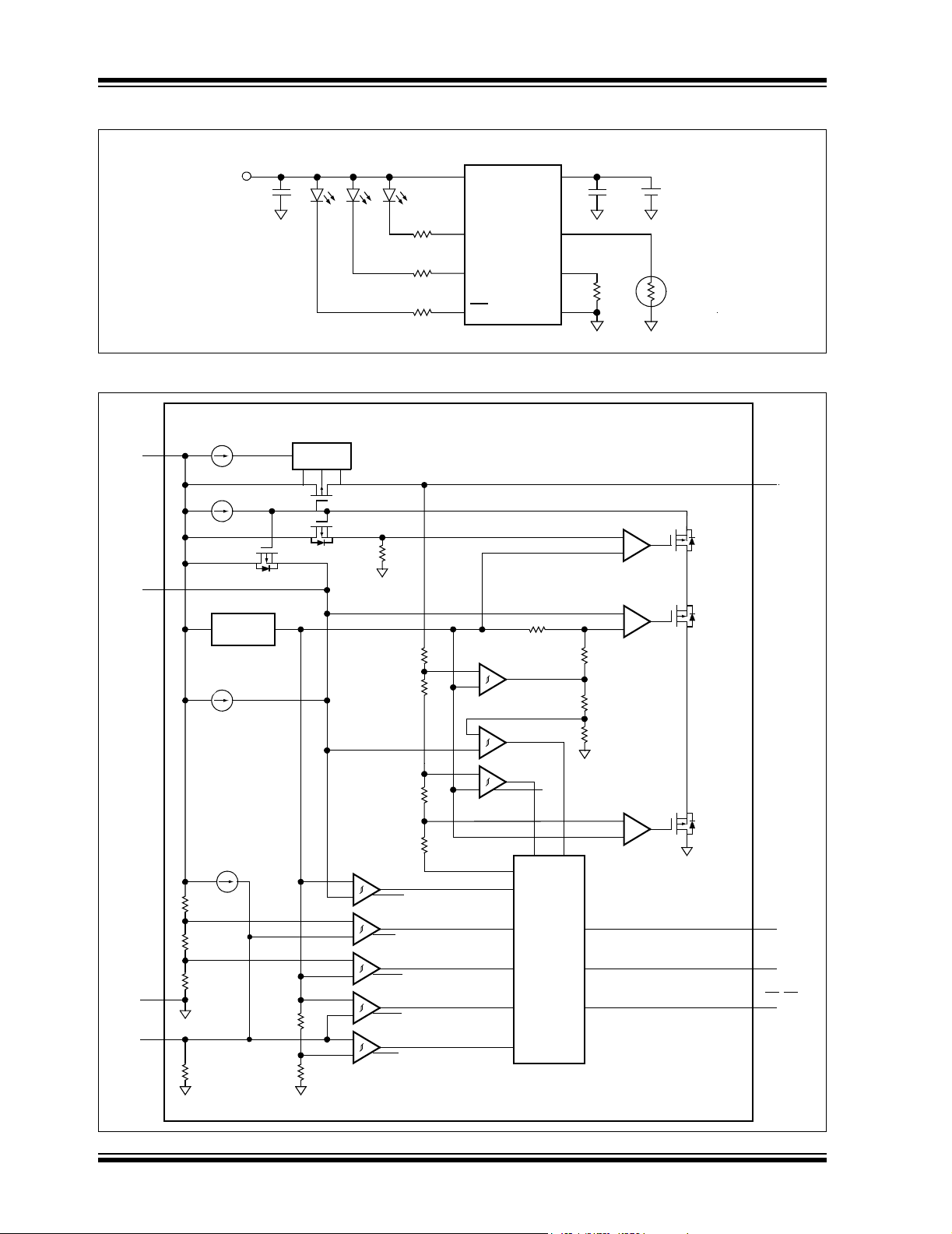
MCP73833/4
Typical Application
V
IN
1µF
Functional Block Diagram
V
DD
10 µA
Direction
Control
1A Li-Ion Battery Charger
1,2
V
DD
38
470Ω
4
470Ω
7
STAT1
STAT2
PG
THERM
PROG
470Ω
MCP73833
9,10
V
BAT
6
5
V
SS
1µF
1kΩ
Single
+
Li-Ion
Cell
T
10 kΩ
V
BAT
PROG
V
SS
THERM
175 kΩ
54 kΩ
121 kΩ
1MΩ
6µA
Reference
Generator
(1.21V)
V
REF
6µA
50 µA
121 kΩ
G=0.001
G=0.001
+
-
+
-
+
-
+
-
+
-
1kΩ
310 kΩ
72.7 kΩ
6kΩ
157.3 kΩ
SHDN
LDO
UVLO
HTVT470.6kΩ
LTV T
111 kΩ
+
PRECONDITION
+
TERMINATIO N
+
-
CHARG E
Charge
Control,
Timer,
and
Status
Logic
10 kΩ
470.6 kΩ
48 kΩ
CURRENT
LIMIT
+
-
CA
+
-
VA
+
-
STAT1
STAT2
PG (TE)
DS22005A-page 2 © 2006 Microchip Technology Inc.
Page 3

MCP73833/4
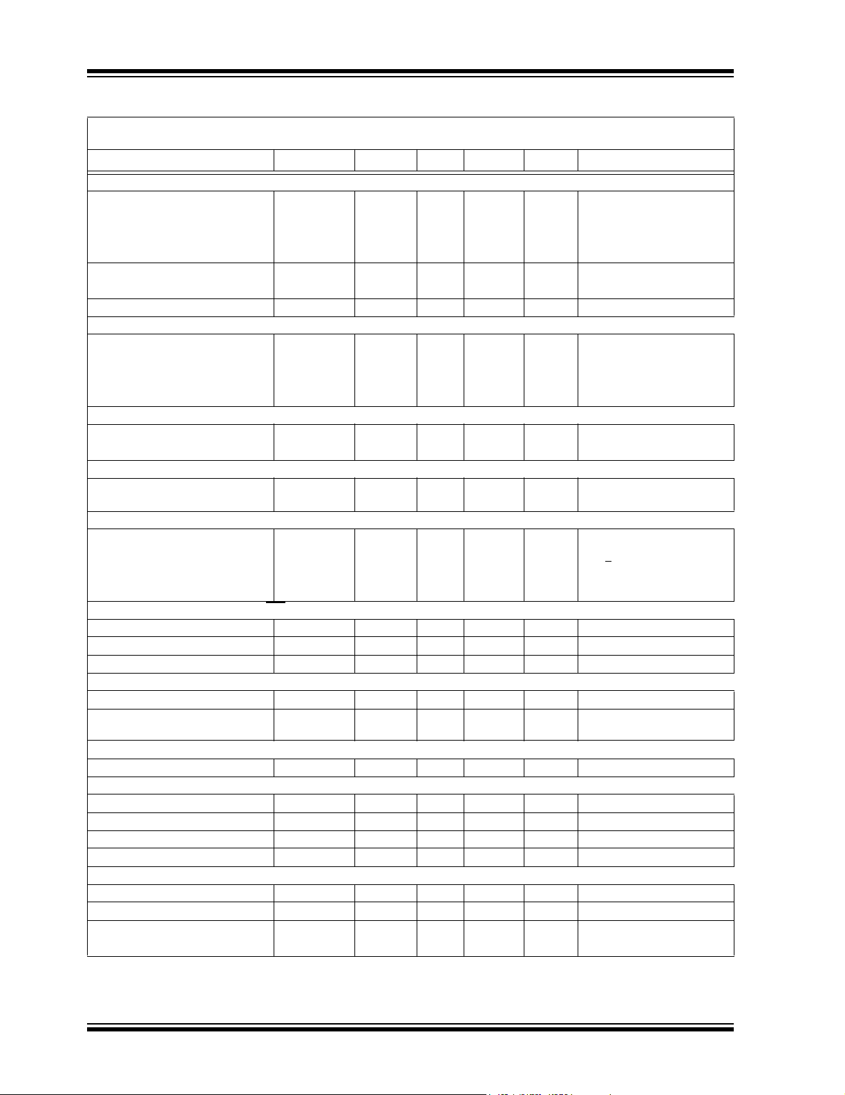
1.0 ELECTRICAL CHARACTERISTICS
*Notice: Stresses above those listed under “Maximum
Ratings” may cause permanent damage to the device.
This is a stress rating only and functional operation of
the device at those or any other conditions above those
Absolute Maximum Ratings
VDD........................................................................7.0V
All Inputs and Outputs w.r.t. V
Maximum Junction Temperature, T
.....-0.3 to (VDD+0.3)V
SS
. Internally Limited
J
indicated in the operational listings of this specification
is not implied. Exposure to maximum rating conditions
for extended periods may affect device reliability.
Storage temperature .......................... -65°C to +150°C
ESD protection on all pins:
Human Body Model (HBM)
(1.5 kΩ in Series with 100 pF)............................... ≥ 4kV
Machine Model (MM)
(200 pF, No Series Resistance) ...........................300V
DC CHARACTERISTICS
Electrical Specifications: Unless otherwise specified, all limits apply for VDD= [V
Typical values are at +25°C, V
DD
= [V
(Typ)+1.0V]
REG
Parameters Sym Min Typ Max Units Conditions
Supply Input
Supply Voltage V
Supply Current I
DD
SS
3.75 — 6 V Charging
V
REG
(Typ)
+0.3V
— 6 V Charge Complete, Standby
— 2000 3000 µA Charging
— 150 300 µA Charge Complete
— 100 300 µA Standby (No Battery or PROG
— 50 100 µA Shutdown (V
UVLO Start Threshold V
UVLO Stop Threshold V
UVLO Hysteresis V
START
STOP
HYS
3.4 3.55 3.7 V VDD Low to High
3.3 3.45 3.6 V VDD High to Low
— 100 — mV
Voltage Regulation (Constant Voltage Mode, System Test Mode)
Regulated Output Voltage V
REG
4.168 4.20 4.232 V VDD=[V
4.318 4.35 4.382 V I
4.367 4.40 4.433 V T
4.467 4.50 4.533 V
)
Line Regulation |(ΔV
Load Regulation |ΔV
BAT/VBAT
/ΔV
DD
/ V
BAT
|
BAT
— 0.10 0.30 %/V V
| — 0.10 0.30 % I
Supply Ripple Attenuation PSRR — 58 — dB I
—47— dBI
—25— dBI
Current Regulation (Fast Charge Constant Current Mode)
Fast Charge Current Regulation I
REG
90 100 110 mA PROG = 10 kΩ
900 1000 1100 mA PROG = 1.0 kΩ
Maximum Output Current Limit I
MAX
— 1200 — mA PROG < 833Ω
(Typ)+0.3V] to 6V, TA=-40°C to 85°C.
REG
Floating)
< V
V
< V
DD
OUT
=-5°C to +55°C
A
=[V
DD
I
OUT
OUT
V
=[V
DD
OUT
OUT
OUT
=-5°C to +55°C
T
A
DD
)
STOP
(Typ)+1V]
REG
=10 mA
(Typ)+1V] to 6V
REG
=10 mA
=10 mA to 100 mA
(Typ)+1V]
REG
=10 mA, 10Hz to 1 kHz
=10 mA, 10Hz to 10 kHz
=10 mA, 10Hz to 1 MHz
BAT
, or
© 2006 Microchip Technology Inc. DS22005A-page 3
Page 4
MCP73833/4
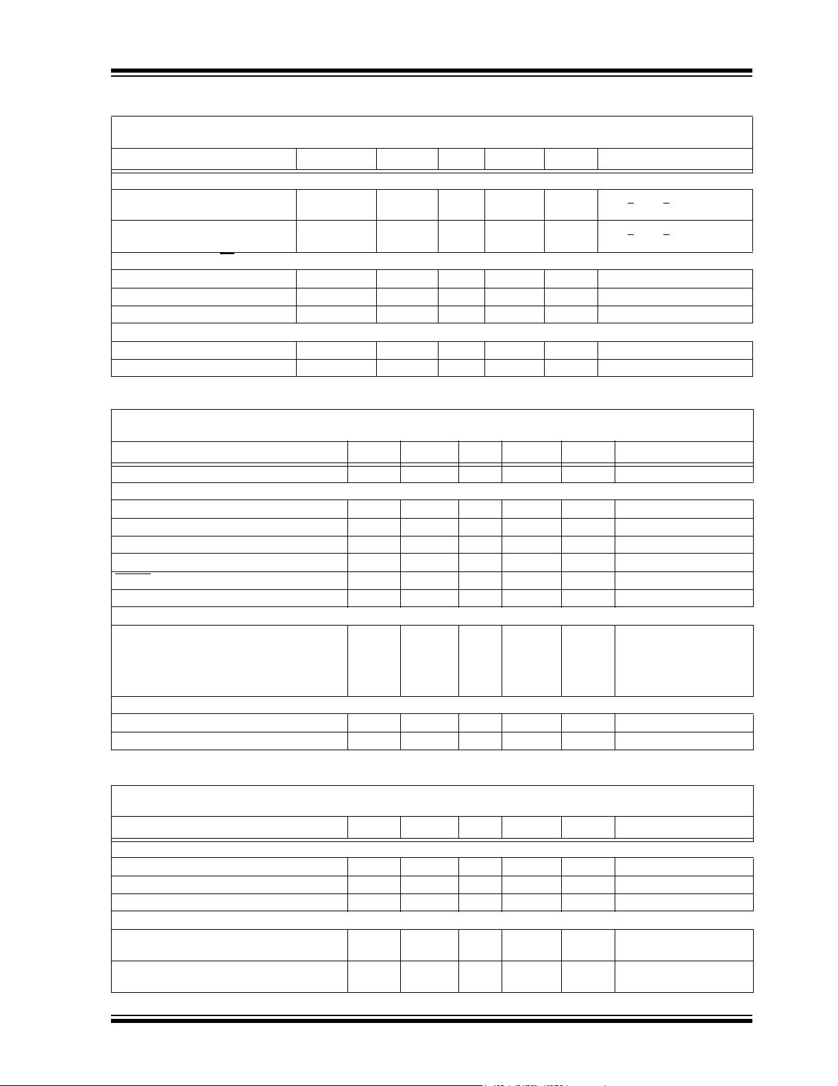
DC CHARACTERISTICS (CONTINUED)
Electrical Specifications: Unless otherwise specified, all limits apply for VDD= [V
Typical values are at +25°C, V
Parameters Sym Min Typ Max Units Conditions
Preconditioning Current Regulation (Trickle Charge Constant Current Mode)
Precondition Current Ratio I
Precondition Voltage Threshold
Ratio
Precondition Hysteresis V
Charge Termination
Charge Termination Current Ratio I
Automatic Recharge
Recharge Voltage Threshold Ratio V
Pass Transistor ON-Resistance
ON-Resistance R
Battery Discharge Current
Output Reverse Leakage Current I
Status Indicators - STAT1, STAT2, PG
Sink Current I
Low Output Voltage V
Input Leakage Current I
PROG Input
Charge Impedance Range R
Standy Impedance R
Thermistor Bias
Thermistor Current Source I
Thermistor Comparator
Upper Trip Threshold V
Upper Trip Point Hysteresis V
Lower Trip Threshold V
Lower Trip Point Hysteresis V
System Test (LDO) Mode
Input High Voltage Level V
THERM Input Sink Current I
Bypass Capacitance C
DD
= [V
(Typ)+1.0V]
REG
PREG
V
PTH
TERM
RTH
DISCHARGE
THERM
T1HYS
T2HYS
/ I
/ V
PHYS
/ I
/ V
DSON
SINK
OL
LK
PROG
PROG
T1
T2
IH
SINK
BAT
REG
REG
REG
REG
7.5 10 12.5 % PROG = 1.0 kΩ to 10 kΩ
15 20 25 % T
30 40 50 %
— 100 — %
64 66.5 70 % V
69 71.5 75 %
— 100 — mV V
3.75 5 6.25 % PROG = 1.0 kΩ to 10 kΩ
5.6 7.5 9.4 % T
7.5 10 12.5 %
15 20 25 %
— 94.0 — % V
— 96.5 — %
— 300 — mΩ VDD = 3.75V
— 0.15 2 µA PROG Floating
—0.25 2 µAV
—0.15 2 µAVDD < V
— -5.5 -15 µA Charge Complete
—1525mA
—0.4 1 VI
— 0.01 1 µA High Impedance, 6V on pin
1—20kΩ
70 — 200 kΩ Minimum Impedance for
47 50 53 µA 2 kΩ < R
1.20 1.23 1.26 V V
—-50—mV
0.235 0.25 0.265 V V
—50—mV
(VDD-0.1)
—— V
3 6 20 µA Stand-by or system test mode
1——µFI
4.7 — — µF I
(Typ)+0.3V] to 6V, TA=-40°C to 85°C.
REG
=-5°C to +55°C
A
Low to High
BAT
High to Low
BAT
=-5°C to +55°C
A
High to Low
BAT
= 105°C
T
J
< V
DD
BAT
STOP
= 4 mA
SINK
Standby
THERM
Low to High
THERM
High to Low
THERM
< 250 mA
OUT
> 250 mA
OUT
< 50 kΩ
DS22005A-page 4 © 2006 Microchip Technology Inc.
Page 5
DC CHARACTERISTICS (CONTINUED)
Electrical Specifications: Unless otherwise specified, all limits apply for VDD= [V
Typical values are at +25°C, V
DD
= [V
(Typ)+1.0V]
REG
Parameters Sym Min Typ Max Units Conditions
Automatic Power Down
Automatic Power Down Entry
Threshold
Automatic Power Down Exit Thresh-
old
Timer Enable Input (TE
)
V
PDEXIT
Input High Voltage Level V
Input Low Voltage Level V
Input Leakage Current I
V
PD
—V
—V
IH
IL
LK
2.0 — — V
——0.6 V
—0.01 1 µAV
+
BAT
50 mV
+
BAT
150 mV
Thermal Shutdown
Die Temperature T
Die Temperature Hysteresis T
SD
SDHYS
— 150 — °C
—10— °C
AC CHARACTERISTICS
Electrical Specifications: Unless otherwise specified, all limits apply for VDD= [V
Typical values are at +25°C, V
Parameters Sym Min Typ Max Units Conditions
UVLO Start Delay t
Current Regulation
Transition Time Out of Preconditioning t
Current Rise Time Out of Preconditioning t
Preconditioning Comparator Filter Time t
Termination Comparator Filter Time t
Comparator Filter Time t
Charge
Thermistor Comparator Filter Time t
Elapsed Timer
Elapsed Timer Period t
Status Indicators
Status Output turn-off t
Status Output turn-on t
DD
= [V
(Typ)+1.0V]
REG
START
DELAY
RISE
PRECON
TERM
CHARGE
THERM
ELAPSED
OFF
ON
—— 5 msV
—— 1 msV
—— 1 msI
0.4 1.3 3.2 ms Average V
0.4 1.3 3.2 ms Average I
0.4 1.3 3.2 ms Average V
0.4 1.3 3.2 ms Average THERM Rise/Fall
0 0 0 Hours Timer Disabled
3.6 4.0 4.4 Hours
5.4 6.0 6.6 Hours
7.2 8.0 8.8 Hours
— — 200 µs I
— — 200 µs I
MCP73833/4
(Typ)+0.3V] to 6V, TA=-40°C to 85°C.
REG
— V 2.3V < V
VDD Falling
— V 2.3V < V
VDD Rising
(Typ)+0.3V] to 6V, TA=-40°C to 85°C.
REG
BAT
BAT
= 6V
TE
Low to High
DD
BAT<VPTH
Rising to 90% of I
OUT
= 1 mA to 0 mA
SINK
= 0 mA to 1 mA
SINK
< V
< V
to V
BAT
OUT
BAT
REG
REG
BAT>VPTH
REG
Rise/Fall
Falling
Falling
TEMPERATURE SPECIFICATIONS
Electrical Specifications: Unless otherwise specified, all limits apply for V
Typical values are at +25°C, V
DD
= [V
(Typ)+1.0V]
REG
Parameters Symbol Min Typ Max Units Conditions
Temperature Ranges
Specified Temperature Range T
Operating Temperature Range T
Storage Temperature Range T
A
A
A
-40 — +85 °C
-40 — +125 °C
-65 — +150 °C
Thermal Package Resistances
Thermal Resistance, MSOP-10 θ
Thermal Resistance, 3mm x 3mm DFN-10 θ
JA
JA
— 113 — °C/W 4-Layer JC51-7 Standard
— 41 — °C/W 4-Layer JC51-7 Standard
© 2006 Microchip Technology Inc. DS22005A-page 5
DD
= [V
REG
(Typ)+0.3V] to 6V.
Board, Natural Convection
Board, Natural Convection
Page 6

MCP73833/4
P
:
:
2.0 TYPICAL PERFORMANCE CURVES
Note: The graphs and tables provided following this note are a statistical summary based on a limited number of
samples and are provided for informational purposes only. The performance characteristics listed herein
are not tested or guaranteed. In some graphs or tables, the data presented may be outside the specified
operating range (e.g., outside specified power supply range) and therefore outside the warranted range.
Note: Unless otherwise indicated, VDD = 5.2V, V
REG
= 4.20V, I
= 10 mA and TA= +25°C, Constant-voltage mode.
OUT
4.210
4.205
4.200
4.195
4.190
(V)
4.185
4.180
4.175
Battery Regulation Voltage
4.170
4.50 4.75 5.00 5.25 5.50 5.75 6.00
Supply Voltage (V)
MCP73833
I
= 10 mA
OUT
I
= 100 mA
OUT
I
= 500 mA
OUT
I
= 900 mA
OUT
FIGURE 2-1: Battery Regulation Voltage
(V
) vs. Supply Voltage (VDD).
BAT
4.220
MCP73833
4.210
4.200
4.190
4.180
I
= 500 mA
4.170
4.160
Battery Regulation Voltage (V)
OUT
I
= 900 mA
OUT
-40
-30
0
-20
-10
Ambient Temperature (°C)
10203040506070
I
OUT
I
OUT
= 10 mA
= 100 mA
80
1000
100
Charge Current (mA)
10
1 3 5 7 9 11 13 15 17 19 21
Programming Resistor (k:)
FIGURE 2-4: Charge Current (I
Programming Resistor (R
104
103
102
101
100
99
98
Charge Current (mA)
97
96
4.50 4.75 5.00 5.25 5.50 5.75 6.00
Supply Voltage (V)
PROG
).
R
PROG
OUT
= 10 k
) vs.
FIGURE 2-2: Battery Regulation Voltage
) vs. Ambient Temperature (TA).
(V
BAT
0.40
A)
0.35
+85°C
0.30
-40°C
0.25
0.20
+25°C
0.15
0.10
0.05
Output Leakage Current (
0.00
3.00 3.20 3.40 3.60 3.80 4.00 4.20
Battery Regulation Voltage (V)
FIGURE 2-3: Output Leakage Current
(I
DISCHARGE
(V
BAT
) vs. Battery Regulation Voltage
).
FIGURE 2-5: Charge Current (I
Supply Voltage (V
1004
1002
1000
998
996
994
992
990
Charge Current (mA)
988
986
4.50 4.75 5.00 5.25 5.50 5.75 6.00
).
DD
Supply Voltage (V)
FIGURE 2-6: Charge Current (I
Supply Voltage (V
DD
).
) vs.
OUT
R
= 1 k
PROG
) vs.
OUT
DS22005A-page 6 © 2006 Microchip Technology Inc.
Page 7

TYPICAL PERFORMANCE CURVES (Continued)
:
:
P
MCP73833/4
Note: Unless otherwise indicated, VDD = 5.2V, V
120
100
80
60
40
20
Charge Current (mA)
0
25354555657585
Junction Temperature (°C)
FIGURE 2-7: Charge Current (I
Junction Temperature (T
1200
1000
800
600
400
200
Charge Current (mA)
0
25354555657585
Junction Temperature (°C)
).
J
R
= 10 k
PROG
95
105
115
125
135
) vs.
OUT
R
= 1 k
PROG
95
105
115
125
135
REG
145
145
= 4.20V, I
155
155
= 10 mA and TA= +25°C, Constant-voltage mode.
OUT
52.0
51.5
51.0
50.5
50.0
49.5
49.0
48.5
48.0
Thermistor Bias Current (µA)
-40
-30
0
-20
Ambient Temperature (°C)
10203040506070
-10
FIGURE 2-10: Thermistor Bias Current
(I
THRERM
) vs. Ambient Temperature (TA).
0
VAC = 100 mVp-p
= 10 mA
I
OUT
-10
= 4.7 µF, X7R
C
OUT
-20
Ceramic
-30
-40
-50
Attenuation (dB)
-60
-70
0.01 0.1 1 10 100 1000
Frequency (kHz)
80
FIGURE 2-8: Charge Current (I
Junction Temperature (T
52.0
A)
51.5
51.0
50.5
50.0
49.5
49.0
48.5
Thermistor Bias Current (
48.0
4.50 4.75 5.00 5.25 5.50 5.75 6.00
).
J
Supply Voltage (V)
FIGURE 2-9: Thermistor Bias Current
(I
THRERM
) vs. Supply Voltage (VDD).
OUT
) vs.
FIGURE 2-11: Power Supply Ripple Rejection (PSRR).
0
VAC = 100 mVp-p
= 100 mA
I
OUT
-10
= 4.7 µF, X7R
C
OUT
Ceramic
-20
-30
-40
Attenuation (dB)
-50
-60
0.01 0.1 1 10 100 1000
Frequency (kHz)
FIGURE 2-12: Power Supply Ripple Rejection (PSRR).
© 2006 Microchip Technology Inc. DS22005A-page 7
Page 8
MCP73833/4
:
:
TYPICAL PERFORMANCE CURVES (Continued)
Note: Unless otherwise indicated, VDD = 5.2V, V
14
12
10
8
6
4
I
2
Source Voltage (V)
0
-2
0
204060
Time (µs)
= 10 mA
OUT
= 4.7 µF, X7R
C
OUT
Ceramic
80
100
120
140
160
180
REG
0.10
0.05
0.00
-0.05
-0.10
-0.15
-0.20
-0.25
-0.30
200
FIGURE 2-13: Line Transient Response.
14
12
10
8
6
4
2
Source Voltage (V)
0
-2
0
204060
80
100
Time (µs)
I
= 100 mA
OUT
= 4.7 µF, X7R
C
OUT
Ceramic
120
140
160
0.10
0.05
0.00
-0.05
-0.10
-0.15
-0.20
-0.25
-0.30
180
200
= 4.20V, I
Output Ripple (V)
Output Ripple (V)
= 10 mA and TA= +25°C, Constant-voltage mode.
OUT
Output Current (A)
1.40
1.20
1.00
0.80
0.60
0.40
0.20
0.00
-0.20
0
C
Ceramic
204060
= 4.7 µF, X7R
OUT
80
Time (µs)
100
120
140
0.10
0.05
0.00
-0.05
-0.10
-0.15
-0.20
-0.25
-0.30
160
180
200
FIGURE 2-16: Load Transient Response.
5.0
4.0
3.0
2.0
MCP73833-FCI/MF
1.0
Battery Voltage (V)
V
= 5.2V
DD
R
= 10.0 k
PROG
0.0
0
30
60
90
Time (Minutes)
120
150
180
200
160
120
80
40
0
210
Output Ripple (V)
Charge Current (A)
FIGURE 2-14: Line Transient Response.
Output Current (A)
0.35
0.30
0.25
0.20
0.15
0.10
0.05
0.00
-0.05
0
204060
C
= 4.7 µF, X7R
OUT
Ceramic
80
Time (µs)
100
120
140
0.04
0.02
0.00
-0.02
-0.04
-0.06
-0.08
-0.10
-0.12
160
180
200
FIGURE 2-15: Load Transient Response.
Output Ripple (V)
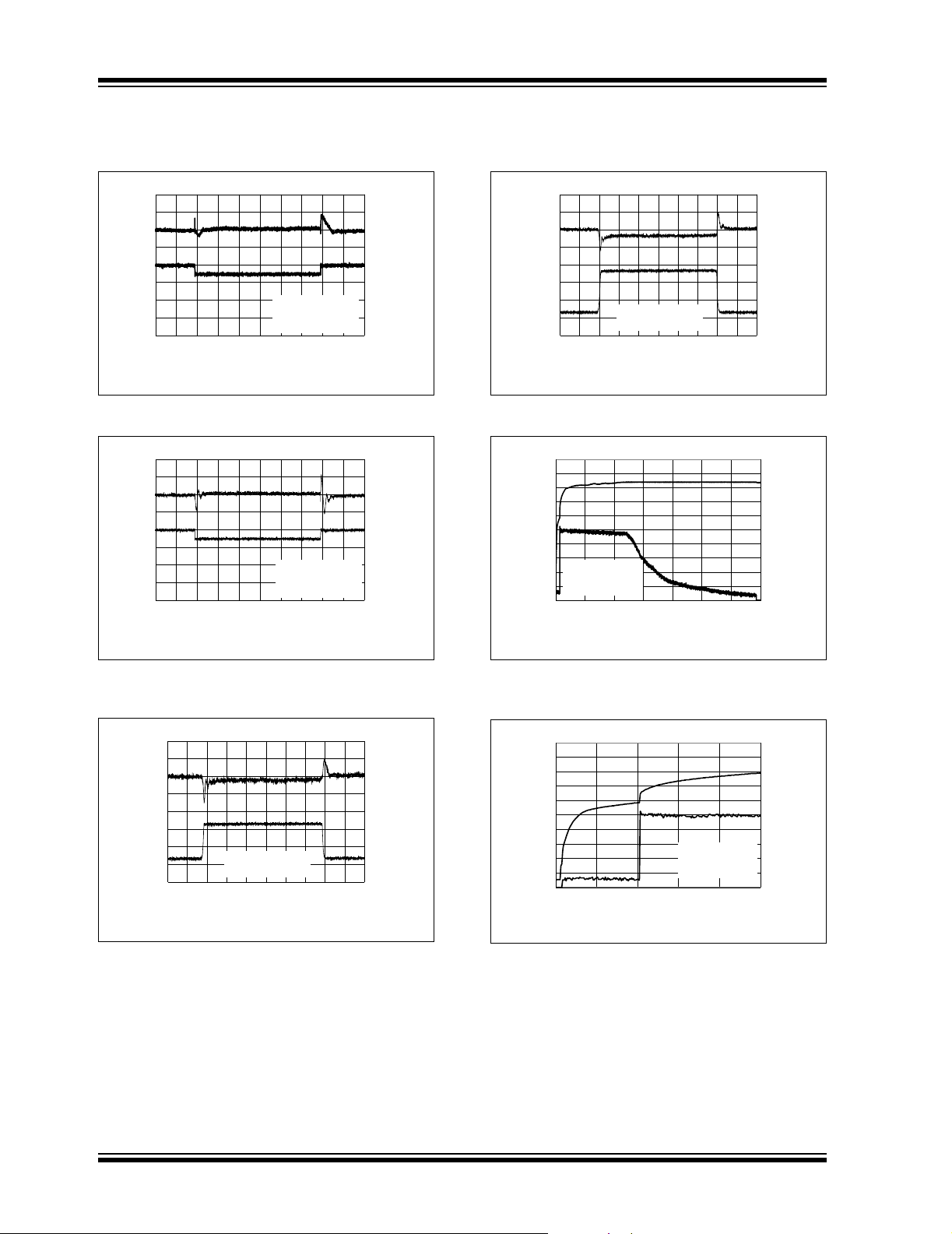
FIGURE 2-17: Complete Charge Cycle
(180 mA Li-Ion Battery).
5.0
4.0
3.0
2.0
Battery Voltage (V)
1.0
0.0
0246810
Time (Minutes)
MCP73833-FCI/MF
V
DD
R
= 10.0 k
PROG
= 5.2V
200
160
120
80
40
0
FIGURE 2-18: Charge Cycle Start Preconditioning (180 mAh Li-Ion Battery).
Charge Current (A)
DS22005A-page 8 © 2006 Microchip Technology Inc.
Page 9

3.0 PIN DESCRIPTIONS
Descriptions of the pins are listed in Table 3-1.
TABLE 3-1: PIN FUNCTION TABLE
MCP73833/4
Pin No.
DFN MSOP
11 V
22 V
3 3 STAT1 Charge Status Output
4 4 STAT2 Charge Status Output
55 V
6 6 PROG Current Regulation Set and Charge Control Enable
77 PG,
8 8 THERM Thermistor input
99 V
10 10 V
3.1 Battery Management Input Supply
)
(V
DD
A supply voltage of [V
recommended. Bypass to VSS with a minimum of 1 µF.
3.2 Charge Status Outputs (STAT1,
STAT2)
STAT1 and STAT2 are open-drain logic outputs for connection to a LED for charge status indication.
Alternatively, a pull-up resistor can be applied for
interfacing to a host microcontroller.
3.3 Battery Management 0V Reference
)
(V
SS
Connect to negative terminal of battery and input
supply.
Symbol Function
DD
DD
SS
TE MCP73833: Power Good output, MCP73834: Timer Enable input
BAT
BAT
Battery Management Input Supply
Battery Management Input Supply
Battery Management 0V Reference
Battery Charge Control Output
Battery Charge Control Output
3.6 Timer Enable Input (TE)
(typ.) + 0.3V] to 6V is
REG
The timer enable (TE) input option is used to enable or
disable the internal timer. A low signal on this pin
enables the internal timer and a high signal disables
the internal timer. The TE
the timer when the charger is supplying current to
charge the battery and power the system load. The TE
input is compatible with 1.8V logic.
3.7 Thermistor Input (THERM)
An internal 50 µA current source provides the bias for
most common 10 kΩ negative-temperature coefficient
thermistors (NTC). The MCP73833/4 compares the
voltage at the THERM pin to factory set thersholds of
1.20V and 0.25V, typically.
MCP73834 Only
3.8 Battery Charge Control Output
3.4 Current Regulation Set (PROG)
Preconditioning, fast charge, and termination currents
are scaled by placing a resistor from PROG to V
The charge management controller can be disabled by
allowing the PROG input to float.
SS
.
Connect to positive terminal of battery. Drain terminal
of internal P-channel MOSFET pass transistor. Bypass
to VSS with a minimum of 1 µF to ensure loop stability
when the battery is disconnected.
(V
BAT
input can be used to disable
)
3.5 Power Good Indication (PG)
MCP73833 Only
The power good (PG) option is a pseudo open-drain
output. The PG
current. However, there is a diode path back to the
input, and, as such, the PG
pulled up to the input. The PG
the input to the MCP73833 is above the UVLO
threshold and greater than the battery voltage.
© 2006 Microchip Technology Inc. DS22005A-page 9
output can sink current, but not source
output should only be
output is low whenever
Page 10

MCP73833/4
4.0 FUNCTIONAL DESCRIPTION
The MCP73833/4 is a highly advanced linear charge
management controller. Refer to the functional block
diagram and Figure 4-1 that depicts the operational
flow algorithm from charge initiation to completion and
automatic recharge.
SYSTEM TEST (LDO) MODE
V
> (VDD - 100 mv)
THERM
PROG > 20 kΩ
STAT1 = LOW
STAT2 = LOW
PG = LOW
Timer Suspended
TEMPERATURE FAULT
No Charge Current
STAT1 = Hi-Z
STAT2 = Hi-Z
PG = LOW
Timer Suspended
SHUTDOWN MODE *
< V
V
DD
UVLO
VDD < V
BAT
STAT1 = HI-Z
STAT2 = HI-Z
PG = HI-Z
STANDBY MODE *
(V
V
BAT
PRECONDITIONING MODE
Charge Current (I
FAST CHARGE MODE
Charge Current (I
+ 100 mv)
REG
PROG > 200 kΩ
STAT1 = HI-Z
STAT2 = HI-Z
PG = LOW
V
BAT
STAT1 = LOW
STAT2 = Hi-Z
PG = LOW
Timer Reset
V
BAT
STAT1 = LOW
STAT2 = Hi-Z
PG = LOW
Timer Enabled
< V
PREG
> V
REG
PTH
PTH
* Continuously Monitored
V
> V
BAT
PTH
Timer Expired
V
< V
BAT
RTH
TIMER FAULT
No Charge Current
STAT1 = Hi-Z
STAT2 = Hi-Z
PG = LOW
Timer Suspended
V
= V
BAT
REG
CONSTANT VOLTAGE MODE
Charge Voltage (V
STAT1 = LOW
STAT2 = Hi-Z
PG = LOW
CHARGE COMPLETE MODE
No Charge Current
STAT1 = HI-Z
STAT2 = LOW
PG = LOW
Timer Reset
REG
V
< I
BAT
TERM
Timer Expired
FIGURE 4-1: Flow Chart.
DS22005A-page 10 © 2006 Microchip Technology Inc.
Page 11

MCP73833/4
4.1 Under Voltage Lockout (UVLO)
An internal under voltage lockout (UVLO) circuit
monitors the input voltage and keeps the charger in
shutdown mode until the input supply rises above the
UVLO threshold. The UVLO circuitry has a built in
hysteresis of 100 mV.
In the event a battery is present when the input power
is applied, the input supply must rise +150 mV above
the battery voltage before the MCP73833/4 becomes
operational.
The UVLO circuit places the device in shutdown mode
if the input supply falls to within +50 mV of the battery
voltage.
The UVLO circuit is always active. At any time the input
supply is below the UVLO threshold or within +50 mV
of the voltage at the V
placed in a shutdown mode.
During any UVLO condition, the battery reverse
discharge current shall be less than 2 µA.
pin, the MCP73833/4 is
BAT
4.2 Charge Qualification
For a charge cycle to begin, all UVLO conditions must
be met and a battery or output load must be present.
A charge current programming resistor must be
connected from PROG to V
or floating, the MCP73833/4 is disabled and the battery
reverse discharge current is less than 2 µA. In this
manner, the PROG pin acts as a charge enable and
can be used as a manual shutdown.
If the input supply voltage is above the UVLO
threshold, but below V
MCP73833/4 will pulse the STAT1 and PG outputs as
the device determines if a battery is present.
. If the PROG pin is open
SS
(Typ)+0.3V, the
REG
4.4 Constant Current - Fast Charge Mode
During the constant current mode, the programmed
charge current is supplied to the battery or load. The
charge current is established using a single resistor
from PROG to V
charge current are calculated using Equation 4-1:
. The program resistor and the
SS
EQUATION 4-1:
1000V
REG
---------------- -=
R
PROG
REG
.
Where:
R
PROG
I
REG
Constant current mode is maintained until the voltage
at the V
When constant current mode is invoked, the internal
timer is reset.
4.4.1 TIMER EXPIRED DURING CONSTANT
If the internal timer expires before the recharge voltage
threshold is reached, a timer fault is indicated and the
charge cycle terminates. The MCP73833/4 remains in
this condition until the battery is removed, the input
power is removed, or the PROG pin is opened. If the
battery is removed or the PROG pin is opened, the
MCP73833/4 enters the Standby mode where it
remains until a battery is reinserted or the PROG pin is
reconnected. If the input power is removed, the
MCP73833/4 is in Shutdown. When the input power is
reapplied, a normal start-up sequence ensues.
pin reaches the regulation voltage, V
BAT
CURRENT - FAST CHARGE MODE
I
= kilo-ohms
= milliampere
4.5 Constant Voltage Mode
4.3 Preconditioning
If the voltage at the V
preconditioning threshold, the MCP73833/4 enters a
preconditioning or trickle charge mode. The
preconditioning threshold is factory set. Refer to
Section 1.0 “Electrical Characteristics” for
preconditioning threshold options.
In this mode, the MCP73833/4 supplies a percentage
of the charge current (established with the value of the
resistor connected to the PROG pin) to the battery. The
percentage or ratio of the current is factory set. Refer to
Section 1.0 “Electrical Characteristics” for
preconditioning current options.
When the voltage at the V
conditioning threshold, the MCP73833/4 enters the
constant current or fast charge mode.
© 2006 Microchip Technology Inc. DS22005A-page 11
pin is less than the
BAT
pin rises above the pre-
BAT
When the voltage at the V
regulation voltage, V
begins. The regulation voltage is factory set to 4.20V,
4.35V, 4.40V, or 4.50V with a tolerance of ± 0.75%.
, constant voltage regulation
REG
4.6 Charge Termination
The charge cycle is terminated when, during constant
voltage mode, the average charge current diminishes
below a percentage of the programmed charge current
(established with the value of the resistor connected to
the PROG pin) or the internal timer has expired. A 1 ms
filter time on the termination comparator ensures that
transient load conditions do not result in premature
charge cycle termination. The percentage or ratio of the
current is factory set. The timer period is factory set
and can be disabled. Refer to Section 1.0 “Electrical
Characteristics” for charge termination current ratio
and timer period options.
The charge current is latched off and the MCP73833/4
enters a charge complete mode.
pin reaches the
BAT
Page 12

MCP73833/4
4.7 Automatic Recharge
The MCP73833/4 continuously monitors the voltage at
the V
pin in the charge complete mode. If the
BAT
voltage drops below the recharge threshold, another
charge cycle begins and current is once again supplied
to the battery or load. The recharge threshold is factory
set. Refer to Section 1.0 “Electrical Characteristics”
for recharge threshold options.
4.8 Thermal Regulation
The MCP73833/4 limits the charge current based on
the die temperature. The thermal regulation optimizes
the charge cycle time while maintaining device reliability. Figure 4-2 depicts the thermal regulation for the
MCP73833/4.
1200
1000
800
600
400
200
Charge Current (mA)
0
25354555657585
Junction Temperature (°C)
R
= 1 k
Ω
PROG
95
105
115
125
135
145
155
4.9 Thermal Shutdown
The MCP73833/4 suspends charge if the die
temperature exceeds +150°C. Charging will resume
when the die temperature has cooled by approximately
+10°C. The thermal shutdown is a secondary safety
feature in the event that there is a failure within the
thermal regulation circuitry.
FIGURE 4-2: Thermal Regulation.
DS22005A-page 12 © 2006 Microchip Technology Inc.
Page 13

MCP73833/4
5.0 DETAILED DESCRIPTION
5.1 Analog Circuitry
5.1.1 BATTERY MANAGEMENT INPUT
SUPPLY (V
The VDD input is the input supply to the MCP73833/4.
The MCP73833/4 automatically enters a Power-down
mode if the voltage on the VDD input falls below the
UVLO voltage (V
the battery pack when the VDD supply is not present.
STOP
5.1.2 CURRENT REGULATION SET
(PROG)
Fast charge current regulation can be scaled by placing
a programming resistor (R
. The program resistor and the charge current
to V
SS
are calculated using the Equation 5-1:
EQUATION 5-1:
Where:
R
PROG
I
REG
The preconditioning trickle-charge current and the
charge termination current are ratiometric to the fast
charge current based on the selected device options.
I
= kilo-ohms
= milliampere
5.1.3 BATTERY CHARGE CONTROL
OUTPUT (V
The battery charge control output is the drain terminal
of an internal P-channel MOSFET. The MCP73833/4
provides constant current and voltage regulation to the
battery pack by controlling this MOSFET in the linear
region. The battery charge control output should be
connected to the positive terminal of the battery pack.
5.1.4 TEMPERATURE QUALIFICATION
(THERM)
The MCP73833/4 continuously monitors battery
temperature during a charge cycle by measuring the
voltage between the THERM and V
50 µA current source provides the bias for most
common 10 kΩ negative-temperature coefficient
(NTC) or positive-temperature coefficient (PTC)
thermistors.The current source is controlled, avoiding
measurement sensitivity to fluctuations in the supply
voltage (V
at the THERM pin to factory set thersholds of 1.20V
and 0.25V, typically. Once a volage outside the
thresholds is detected during a charge cycle, the
MCP73833/4 immediately suspends the charge cycle.
The MCP73833/4 suspends charge by turning off the
). The MCP73833/4 compares the voltage
DD
)
DD
). This feature prevents draining
) from the PROG input
PROG
1000V
---------------- -=
REG
R
PROG
)
BAT
pins. An internal
SS
pass transistor and holding the timer value. The charge
cycle resumes when the voltage at the THERM pin
returns to the normal range.
If temperature monitoring is not required, place a
standard 10 kΩ resistor from THERM to V
SS
5.1.4.1 System Test (LDO) Mode
The MCP73833/4 can be placed in a system test mode.
In this mode, the MCP73833/4 operates as a low
dropout linear regulator (LDO). The output voltage is
regulated to the factory set voltage regulation option.
The available output current is limitted to the
programmed fast charge current. For stability, the V
output must be bypassed to VSS with a minimum
capacitance of 1 µF for output currents up to 250 mA.
A minimum capacitance of 4.7 µF is required for output
currents above 250 mA.
The system test mode is entered by driving the THERM
input greater than (V
connected to the output. In this mode, the MCP73833/4
can be used to power the system without a battery
present.
Note 1: I
THERM
stand-by, and system test modes.
2: A pull-down current source on the
THERM input is active only in stand-by
and system test modes.
3: During system test mode, the PROG
input sets the available output current
limit.
4: System test mode shall be exited by
releasing the THERM input or cycling
input power.
-100 mV) with no battery
DD
is disabled during shutdown,
BAT
5.2 Digital Circuitry
5.2.1 STATUS INDICATORS AND POWER
GOOD (PG
The charge status outputs have two different states:
Low (L), and High Impedance (Hi-Z). The charge status
outputs can be used to illuminate LEDs. Optionally, the
charge status outputs can be used as an interface to a
host microcontroller. Table 5-1 summarize the state of
the status outputs during a charge cycle.
TABLE 5-1: STATUS OUTPUTS
CHARGE CYCLE STATE STAT1 STAT2 PG
Shutdown Hi-Z Hi-Z Hi-Z
Standby Hi-Z Hi-Z L
Charge in Progress L Hi-Z L
Charge Complete (EOC) Hi-Z L L
Temperature Fault Hi-Z Hi-Z L
Timer Fault Hi-Z Hi-Z L
System Test Mode L L L
- OPTION)
© 2006 Microchip Technology Inc. DS22005A-page 13
Page 14

MCP73833/4
5.2.2 POWER GOOD (PG) OPTION
The power good (PG) option is a pseudo open-drain
output. The PG
current. However, there is a diode path back to the
input, and as such, the PG output should only be pulled
up to the input. The PG
input to the MCP73833 is above the UVLO threshold
and greater than the battery voltage. If the supply voltage is above the UVLO, but below V
the MCP73833 will pulse the PG output as the device
determines if a battery is present.
output can sink current, but not source
output is low whenever the
(Typ)+0.3V,
REG
5.2.3 TIMER ENABLE (TE) OPTION
The timer enable (TE) input option is used to enable or
disable the internal timer. A low signal on this pin
enables the internal timer and a high signal disables
the internal timer. The TE
the timer when the charger is supplying current to
charge the battery and power the system load. The TE
input is compatible with 1.8V logic.
input can be used to disable
5.2.4 DEVICE DISABLE (PROG)
The current regulation set input pin (PROG) can be
used to terminate a charge at any time during the
charge cycle, as well as to initiate a charge cycle or
initiate a recharge cycle.
Placing a programming resistor from the PROG input to
enables the device. Allowing the PROG input to
V
SS
float or by applying a logic-high input signal, disables
the device and terminates a charge cycle. When
disabled, the device’s supply current is reduced to
100 µA, typically.
DS22005A-page 14 © 2006 Microchip Technology Inc.
Page 15

6.0 APPLICATIONS
:
:
The MCP73833/4 is designed to operate in conjunction
with a host microcontroller or in stand-alone applications. The MCP73833/4 provides the preferred charge
algorithm for Lithium-Ion and Lithium-Polymer cells
C
IN
LED
Regulated
Wall Cube
FIGURE 6-1: Typical Application Circuit.
LED LED
Constant-current followed by Constant-voltage.
Figure 6-1 depicts a typical stand-alone application
circuit, while Figures 6-2 and 6-3 depict the
accompanying charge profile.
Li-Ion Battery Charger
1,2
V
DD
38
STAT1
STAT2
PG
THERM
PROG
R
LED
4
R
LED
7
R
LED
MCP73833
9,10
V
BAT
6
5
V
SS
MCP73833/4
+
Single
Li-Ion
-
Cell
10 kΩT
R
C
T1
R
OUT
PROG
R
T2
5.0
4.0
3.0
2.0
MCP73833-FCI/MF
1.0
Battery Voltage (V)
V
= 5.2V
DD
R
= 1.00 k
PROG
0.0
0
20
40
60
Time (Minutes)
80
100
120
140
2.00
1.60
1.20
0.80
0.40
Charge Current (A)
0.00
160
FIGURE 6-2: Typical Charge Profile with
Thermal Regulation (1700 mAh Li-Ion Battery).
5.0
4.0
3.0
2.0
Battery Voltage (V)
1.0
0.0
0
2
MCP73833-FCI/MF
4
6
Time (Minutes)
V
DD
R
= 1.00 k
PROG
= 5.2V
8
2.00
1.60
1.20
0.80
Charge Current (A)
0.40
0.00
10
6.1 Application Circuit Design
Due to the low efficiency of linear charging, the most
important factors are thermal design and cost, which
are a direct function of the input voltage, output current
and thermal impedance between the battery charger
and the ambient cooling air. The worst-case situation is
when the device has transitioned from the
Preconditioning mode to the Constant-current mode. In
this situation, the battery charger has to dissipate the
maximum power. A trade-off must be made between
the charge current, cost and thermal requirements of
the charger.
6.1.1 COMPONENT SELECTION
Selection of the external components in Figure 6-1 is
crucial to the integrity and reliability of the charging
system. The following discussion is intended as a guide
for the component selection process.
6.1.1.1 Current Programming Resistor
(R
The preferred fast charge current for Lithium-Ion cells
is at the 1C rate, with an absolute maximum current at
the 2C rate. For example, a 500 mAh battery pack has
a preferred fast charge current of 500 mA. Charging at
this rate provides the shortest charge cycle times
without degradation to the battery pack performance or
life.
PROG
)
FIGURE 6-3: Typical Charge Cycle Start
with Thermal Regulation (1700 mAh Li-Ion
Battery).
© 2006 Microchip Technology Inc. DS22005A-page 15
Page 16

MCP73833/4
6.1.1.2 Thermal Considerations
The worst-case power dissipation in the battery
charger occurs when the input voltage is at the
maximum and the device has transitioned from the
Preconditioning mode to the Constant-current mode. In
this case, the power dissipation is:
PowerDissipation V
–()I
DDMAXVPTHMIN
×=
REGMAX
Where:
V
DDMAX
I
REGMAX
V
PTHMIN
= the maximum input voltage
= the maximum fast charge current
= the minimum transition threshold
voltage
Power dissipation with a 5V, ±10% input voltage source
is:
PowerDissipation 5.5V 2.7 V–()550mA× 1.54W==
This power dissipation with the battery charger in the
MSOP-10 package will cause thermal regulation to be
entered as depicted in Figure 6-3. Alternatively, the
3 mm x 3 mm DFN package could be utilized to reduce
charge cycle times.
6.1.1.3 External Capacitors
The MCP73833/4 is stable with or without a battery
load. In order to maintain good AC stability in the Constant-voltage mode, a minimum capacitance of 4.7 µF
is recommended to bypass the V
pin to VSS. This
BAT
capacitance provides compensation when there is no
battery load. In addition, the battery and interconnections appear inductive at high frequencies. These
elements are in the control feedback loop during
Constant-voltage mode. Therefore, the bypass
capacitance may be necessary to compensate for the
inductive nature of the battery pack.
Virtually any good quality output filter capacitor can be
used, independent of the capacitor’s minimum
Effective Series Resistance (ESR) value. The actual
value of the capacitor (and its associated ESR)
depends on the output load current. A 4.7 µF ceramic,
tantalum or aluminum electrolytic capacitor at the
output is usually sufficient to ensure stability for output
currents up to a 500 mA.
6.1.1.4 Reverse-Blocking Protection
The MCP73833/4 provides protection from a faulted or
shorted input. Without the protection, a faulted or
shorted input would discharge the battery pack through
the body diode of the internal pass transistor.
6.1.1.5 Charge Inhibit
The current regulation set input pin (PROG) can be
used to terminate a charge at any time during the
charge cycle, as well as to initiate a charge cycle or
initiate a recharge cycle.
Placing a programming resistor from the PROG input to
enables the device. Allowing the PROG input to
V
SS
float or by applying a logic-high input signal, disables
the device and terminates a charge cycle. When
disabled, the device’s supply current is reduced to
100 µA, typically.
6.1.1.6 Temperature Monitoring
The charge temperature window can be set by placing
fixed value resistors in series-parallel with a thermistor.
The resistance values of R
and RT2 can be
T1
calculated with the following equations in order to set
the temperature window of interest.
For NTC thermistors:
RT2R
×
COLD
24k
Ω
5k Ω R
R
T1
T1
---------------------------------+=
RT2R
+
RT2R
×
-----------------------------+=
R
+
T2RHOT
COLD
HOT
Where:
R
is the fixed series resistance
T1
is the fixed parallel resistance
R
T2
is the thermistor resistance at the
R
COLD
lower temperature of interest
is the thermistor resistance at the upper
R
HOT
temperature of interest.
For example, by utilizing a 10 kΩ at 25C NTC
thermistor with a sensitivity index, β, of 3892, the
charge temperature range can be set to 0C - 50C by
placing a 1.54 kΩ resistor in series (R
), and a
T1
69.8 kΩ resistor in parallel (RT2) with the thermistor as
depicted in Figure 6-1.
6.1.1.7 Charge Status Interface
A status output provides information on the state of
charge. The output can be used to illuminate external
LEDs or interface to a host microcontroller. Refer to
Table 5-1 for a summary of the state of the status
output during a charge cycle.
DS22005A-page 16 © 2006 Microchip Technology Inc.
Page 17

6.2 PCB Layout Issues
For optimum voltage regulation, place the battery pack
as close as possible to the device’s V
recommended to minimize voltage drops along the
high current-carrying PCB traces.
If the PCB layout is used as a heatsink, adding many
vias in the heatsink pad can help conduct more heat to
the backplane of the PCB, thus reducing the maximum
junction temperature. Figures 6-4 and 6-5 depict a
typical layout with PCB heatsinking.
MCP73833
V
SS
C
IN
V
DD
STAT1
STAT2
R
PROG
and VSS pins,
BAT
C
V
THERM
PG
OUT
BAT
MCP73833/4
FIGURE 6-4: Typical Layout (Top).
V
SS
V
DD
V
BAT
FIGURE 6-5: Typical Layout (Bottom).
© 2006 Microchip Technology Inc. DS22005A-page 17
Page 18

MCP73833/4
7.0 PACKAGING INFORMATION
7.1 Package Marking Information
10-Lead DFN
1
XXXX
2
XYWW
3
NNN
4
56
10
9
8
7
10-Lead MSOP
XXXXXX
YWWNNN
Part Number *
Marking
Code
Part Number *
Marking
Code
MCP73833-AMI/MF AAAA
MCP73833-BZI/MF AAAB
MCP73833-FCI/MF AAAC MCP73834-FCI/MF BAAC
MCP73833-GPI/MF AAAD MCP73834-GPI/MF BAAD
MCP73833-NVI/MF AAAF MCP73834-NVI/MF BAAF
MCP73833-CNI/MF AAAK MCP73834-CNI/MF BAAK
* Consult Factory for Alternative Device Options.
Part Number *
Marking
Code
Part Number *
Marking
Code
MCP73833-AMI/UN 833AMI
MCP73833-BZI/UN 833BZI
MCP73833-FCI/UN 833FCI MCP73834-FCI/UN 834FCI
MCP73833-GPI/UN 833GPI MCP73834-GPI/UN 834GPI
MCP73833-NVI/UN 833NVI MCP73834-NVI/UN 834NVI
MCP73833-CNI/UN 833CNI MCP73834-CNI/UN 834CNI
* Consult Factory for Alternative Device Options.
Example:
1
AAAA
2
0633
3
256
4
56
10
9
8
7
Example:
8336SI
633256
Legend: XX...X Customer-specific information
Y Year code (last digit of calendar year)
YY Year code (last 2 digits of calendar year)
WW Week code (week of January 1 is week ‘01’)
NNN Alphanumeric traceability code
3
e
Pb-free JEDEC designator for Matte Tin (Sn)
* This package is Pb-free. The Pb-free JEDEC designator ( )
3
e
can be found on the outer packaging for this package.
Note: In the event the full Microchip part number cannot be marked on one line, it will
be carried over to the next line, thus limiting the number of available
characters for customer-specific information.
DS22005A-page 18 © 2006 Microchip Technology Inc.
Page 19

MCP73833/4
10-Lead Plastic Dual-Flat No-Lead Package (MF) 3x3x0.9 mm Body (DFN) – Saw Singulated
Note: For the most current package drawings, please
see the Microchip Packaging Specification located
at http://www.microchip.com/packaging
E
A
INCHES
NOM
K
EXPOSED
METAL
PAD
(
NOTE 2
EXPOSED
TIE BAR
(
NOTE 3
10
.035
.001
.118
.094
.118
.065
.010
.016
)
MAX
BOTTOM VIEW
)
MILLIMETERS
MIN
.039
.002
.124
.096
.124
.067
.015
.020
0.80
0.00
2.85
2.08
2.85
1.30
0.18
0.30
D
PIN 1
ID INDEX
AREA
NOTE 1
(
A3
Number of Pins
Pitch
Overall Height
Standoff
Lead Thickness
Overall Length
Exposed Pad Length
Overall Width
Exposed Pad Width
Lead Width
Contact Length §
Contact-to-Exposed Pad § K .008 — — 0.20 — —
*
Controlling Parameter
§
Significant Characteristic
Notes:
1.
Pin 1 visual index feature may vary, but must be located within the hatched area.
2.
Exposed pad varies according to die attach paddle size.
3.
Package may have one or more exposed tie bars at ends.
BSC: Basic Dimension. Theoretically exact value shown without tolerances.
See ASME Y14.5M
REF: Reference Dimension, usually without tolerance, for information purposes only.
See ASME Y14.5M
JEDEC equivalent: Not Registered
Drawing No. C04-063
)
TOP VIEW
Dimension Limits
(
Note 3
Note 3
)
(
A1
Units
MIN
n
e
A
A1
A3
E
)
E2
D
D2
b
L
.020 BSC
.031
.000
.008 REF.
.112
.082
.112
.051
.008
.012
pb
n
21
E2
NOM
10
0.50 BSC
0.90
0.02
0.20 REF.
3.00
2.39
3.00
1.65
0.25
0.40
Revised 09-12-05
D2
*
MAX
1.00
0.05
3.15
2.45
3.15
1.70
0.30
0.50
L
© 2006 Microchip Technology Inc. DS22005A-page 19
Page 20

MCP73833/4
10-Lead Plastic Micro Small Outline Package (UN) (MSOP)
Note: For the most current package drawings, please
see the Microchip Packaging Specification located
at http://www.microchip.com/packaging
E
E1
p
D
2
n
B
1
α
c
L
β
Units
Dimension Limits
Number of Pins
Pitch
Overall Height
Molded Package Thickness
Standoff
Overall Width
Molded Package Width
Overall Length
Foot Length
Foot Angle
Lead Thickness
Lead Width
Mold Draft Angle Top
Mold Draft Angle Bott om
*
Controlling Parameter
Notes:
Dimensions D and E1 do not include mold flash or protrusions. Mold flash or protrusions shall not exceed .010" (0.254 mm) per side.
BSC: Basic Dimension. Theoretically exact value shown without tolerances.
See ASME Y14.5M
REF: Reference Dimension, usually witho ut tolerance, for information purposes only.
See ASME Y14.5M
JEDEC Equivalent: MO-187 BA
Drawing No. C04-021
n
p
A
A2
A1
E
E1
D
L
φ
c
B
α
β
(F)
MIN
.030
.000
.016 .024
0° – 8°
.003
.006
5° –
5° –
INCHES
NOM
.020 BSC
.193 BSC
.118 BSC
.118 BSC
.037 REFFFootprint
φ
10
.033
.009
A
A1
MAX NOM
.043
.037
.006
.031
–
.009
.012
MIN
15°
15°
MILLIMETERS
0.50 BSC
–
0.75
0.00
4.90 BSC
3.00 BSC
3.00 BSC
0.40
0.95 REF
0.08
0.15
5° 15°
5° 15°
Revised 09-16-05
*
MAX
10
–
0.85
0.60
–
–
0.23
–
–
A2
1.10
0.95
0.15
0.80
8°0°
0.23
0.30
DS22005A-page 20 © 2006 Microchip Technology Inc.
Page 21

APPENDIX A: REVISION HISTORY
Revision A (September 2006)
• Original Release of this Document.
MCP73833/4
© 2006 Microchip Technology Inc. DS22005A-page 23
Page 22

MCP73833/4
NOTES:
DS22005A-page 24 © 2006 Microchip Technology Inc.
Page 23

MCP73833/4
PRODUCT IDENTIFICATION SYSTEM
To order or obtain information, e.g., on pricing or delivery, refer to the factory or the listed sales office.
PART NO. XX
Device
Output
X/
Tem p.XXPackage
Options*
Device: MCP73833: 1A Fully Integrated Charger,
MCP73833T: 1A Fully Integrated Charger,
MCP73834: 1A Fully Integrated Charger,
MCP73834T: 1A Fully Integrated Charger,
Output Options * * * Refer to table below for different operational options.
* * Consult Factory for Alternative Device Options.
Temperature: I = -40°C to +85°C
function on pin 7
PG
PG
function on pin 7
(Tape and Reel)
function on pin 7
TE
function on pin 7
TE
(Tape and Reel)
Examples: * *
a) MCP73833-AMI/UN: 10-lead MSOP pkg.
b) MCP73833-BZI/UN: 10-lead MSOP pkg.
c) MCP73833-CNI/MF: 10-lead DFN pkg.
d) MCP73833-FCI/UN: 10-lead MSOP pkg.
e) MCP73833-GPI/UN: 10-lead MSOP pkg.
f) MCP73833-NVI/MF: 10-lead DFN pkg.
a) MCP73834-CNI/MF: 10-lead DFN pkg.
b) MCP73834-FCI/UN: 10-lead MSOP pkg.
c) MCP73834-GPI/UN: 10-lead MSOP pkg.
d) MCP73834-NVI/MF: 10-lead DFN pkg.
* * Consult Factory for Alternative Device Options
Package Type: MF = Plastic Dual Flat No Lead (DFN)
Part Number V
(3x3x0.9 mm Body), 10-lead
UN = Plastic Micro Small Outline Package (MSOP),
10-lead
REG
I
PREG/IREG
V
PTH/VREG
I
TERM/IREG
V
RTH/VREG
Timer Period
MCP73833-AMI/MF 4.20V 10% 71.5% 7.5% 96.5% 0 hours
MCP73833-BZI/MF 4.20V 100% N/A 7.5% 96.5% 0 hours
MCP73833-CNI/MF 4.20V 10% 71.5% 20% 94% 4 hours
MCP73833-FCI/MF 4.20V 10% 71.5% 7.5% 96.5% 6 hours
MCP73833-GPI/MF 4.20V 100% N/A 7.5% 96.5% 6 hours
MCP73833-NVI/MF 4.35V 10% 71.5% 7.5% 96.5% 6 hours
MCP73833-AMI/UN 4.20V 10% 71.5% 7.5% 96.5% 0 hours
MCP73833-FCI/UN 4.20V 10% 71.5% 7.5% 96.5% 6 hours
MCP73834-BZI/MF 4.20V 100% N/A 7.5% 96.5% 0 hours
MCP73834-CNI/MF 4.20V 10% 71.5% 20% 94% 4 hours
MCP73834-FCI/MF 4.20V 10% 71.5% 7.5% 96.5% 6 hours
MCP73834-NVI/MF 4.35V 10% 71.5% 7.5% 96.5% 6 hours
MCP73834-FCI/UN 4.20V 10% 71.5% 7.5% 96.5% 6 hours
© 2006 Microchip Technology Inc. DS22005A-page 25
Page 24

MCP73833/4
NOTES:
DS22005A-page 26 © 2006 Microchip Technology Inc.
Page 25

Note the following details of the code protection feature on Microchip devices:
• Microchip products meet the specification contained in their particular Microchip Data Sheet.
• Microchip believes that its family of products is one of the most secure families of its kind on the market today, when used in the
intended manner and under normal conditions.
• There are dishonest and possibly illegal methods used to breach the code protection feature. All of these methods, to our
knowledge, require using the Microchip products in a manner outside the operating specifications contained in Microchip’s Data
Sheets. Most likely, the person doing so is engaged in theft of intellectual property.
• Microchip is willing to work with the customer who is concerned about the integrity of their code.
• Neither Microchip nor any other semiconductor manufacturer can guarantee the security of their code. Code protection does not
mean that we are guaranteeing the product as “unbreakable.”
Code protection is constantly evolving. We at Microchip are committed to continuously improving the code protection features of our
products. Attempts to break Microchip’s code protection feature may be a violation of the Digital Millennium Copyright Act. If such acts
allow unauthorized access to your software or other copyrighted work, you may have a right to sue for relief under that Act.
Information contained in this publication regarding device
applications and the like is provided only for your convenience
and may be superseded by updates. It is your responsibility to
ensure that your application meets with your specifications.
MICROCHIP MAKES NO REPRESENTATIONS OR
WARRANTIES OF ANY KIND WHETHER EXPRESS OR
IMPLIED, WRITTEN OR ORAL, STATUTORY OR
OTHERWISE, RELATED TO THE INFORMATION,
INCLUDING BUT NOT LIMITED TO ITS CONDITION,
QUALITY, PERFORMANCE, MERCHANTABILITY OR
FITNESS FOR PURPOSE. Microchip disclaims all liability
arising from this information and its use. Use of Microchip
devices in life support and/or safety applications is entirely at
the buyer’s risk, and the buyer agrees to defend, indemnify and
hold harmless Microchip from any and all damages, claims,
suits, or expenses resulting from such use. No licenses are
conveyed, implicitly or otherwise, under any Microchip
intellectual property rights.
Trademarks
The Microchip name and logo, the Microchip logo, Accuron,
dsPIC, K
EELOQ, microID, MPLAB, PIC, PICmicro, PICSTART,
PRO MATE, PowerSmart, rfPIC, and SmartShunt are
registered trademarks of Microchip Technology Incorporated
in the U.S.A. and other countries.
AmpLab, FilterLab, Migratable Memory, MXDEV, MXLAB,
SEEVAL, SmartSensor and The Embedded Control Solutions
Company are registered trademarks of Microchip Technology
Incorporated in the U.S.A.
Analog-for-the-Digital Age, Application Maestro, CodeGuard,
dsPICDEM, dsPICDEM.net, dsPICworks, ECAN,
ECONOMONITOR, FanSense, FlexROM, fuzzyLAB,
In-Circuit Serial Programming, ICSP, ICEPIC, Linear Active
Thermistor, Mindi, MiWi, MPASM, MPLIB, MPLINK, PICkit,
PICDEM, PICDEM.net, PICLAB, PICtail, PowerCal,
PowerInfo, PowerMate, PowerTool, REAL ICE, rfLAB,
rfPICDEM, Select Mode, Smart Serial, SmartTel, Total
Endurance, UNI/O, WiperLock and ZENA are trademarks of
Microchip Technology Incorporated in the U.S.A. and other
countries.
SQTP is a service mark of Microchip Technology Incorporated
in the U.S.A.
All other trademarks mentioned herein are property of their
respective companies.
© 2006, Microchip Technology Incorporated, Printed in the
U.S.A., All Rights Reserved.
Printed on recycled paper.
Microchip received ISO/TS-16949:2002 certification for its worldwide
headquarters, design and wafer fabrication facilities in Chandler and
Tempe, Arizona, Gresham, Oregon and Mountain View, California. The
Company’s quality system processes and procedures are for its
PICmicro
EEPROMs, microperipherals, nonvolatile memory and analog
products. In addition, Microchip’s quality system for the design and
manufacture of development systems is ISO 9001:2000 certified.
®
8-bit MCUs, KEELOQ
®
code hopping devices, Serial
© 2006 Microchip Technology Inc. DS22005A-page 27
Page 26

WORLDWIDE SALES AND SERVICE
AMERICAS
Corporate Office
2355 West Chandler Blvd.
Chandler, AZ 85224-6199
Tel: 480-792-7200
Fax: 480-792-7277
Technical Support:
http://support.microchip.com
Web Address:
www.microchip.com
Atlanta
Alpharetta, GA
Tel: 770-640-0034
Fax: 770-640-0307
Boston
Westborough, MA
Tel: 774-760-0087
Fax: 774-760-0088
Chicago
Itasca, IL
Tel: 630-285-0071
Fax: 630-285-0075
Dallas
Addison, TX
Tel: 972-818-7423
Fax: 972-818-2924
Detroit
Farmington Hills, MI
Tel: 248-538-2250
Fax: 248-538-2260
Kokomo
Kokomo, IN
Tel: 765-864-8360
Fax: 765-864-8387
Los Angeles
Mission Viejo, CA
Tel: 949-462-9523
Fax: 949-462-9608
Santa Clara
Santa Clara, CA
Tel: 408-961-6444
Fax: 408-961-6445
Toronto
Mississauga, Ontario,
Canada
Tel: 905-673-0699
Fax: 905-673-6509
ASIA/PACIFIC
Asia Pacific Office
Suites 3707-14, 37th Floor
Tower 6, The Gateway
Habour City, Kowloon
Hong Kong
Tel: 852-2401-1200
Fax: 852-2401-3431
Australia - Sydney
Tel: 61-2-9868-6733
Fax: 61-2-9868-6755
China - Beijing
Tel: 86-10-8528-2100
Fax: 86-10-8528-2104
China - Chengdu
Tel: 86-28-8665-5511
Fax: 86-28-8665-7889
China - Fuzhou
Tel: 86-591-8750-3506
Fax: 86-591-8750-3521
China - Hong Kong SAR
Tel: 852-2401-1200
Fax: 852-2401-3431
China - Qingdao
Tel: 86-532-8502-7355
Fax: 86-532-8502-7205
China - Shanghai
Tel: 86-21-5407-5533
Fax: 86-21-5407-5066
China - Shenyang
Tel: 86-24-2334-2829
Fax: 86-24-2334-2393
China - Shenzhen
Tel: 86-755-8203-2660
Fax: 86-755-8203-1760
China - Shunde
Tel: 86-757-2839-5507
Fax: 86-757-2839-5571
China - Wuhan
Tel: 86-27-5980-5300
Fax: 86-27-5980-5118
China - Xian
Tel: 86-29-8833-7250
Fax: 86-29-8833-7256
ASIA/PACIFIC
India - Bangalore
Tel: 91-80-4182-8400
Fax: 91-80-4182-8422
India - New Delhi
Tel: 91-11-4160-8631
Fax: 91-11-4160-8632
India - Pune
Tel: 91-20-2566-1512
Fax: 91-20-2566-1513
Japan - Yokohama
Tel: 81-45-471- 6166
Fax: 81-45-471-6122
Korea - Gumi
Tel: 82-54-473-4301
Fax: 82-54-473-4302
Korea - Seoul
Tel: 82-2-554-7200
Fax: 82-2-558-5932 or
82-2-558-5934
Malaysia - Penang
Tel: 60-4-646-8870
Fax: 60-4-646-5086
Philippines - Manila
Tel: 63-2-634-9065
Fax: 63-2-634-9069
Singapore
Tel: 65-6334-8870
Fax: 65-6334-8850
Taiwan - Hsin Chu
Tel: 886-3-572-9526
Fax: 886-3-572-6459
Taiwan - Kaohsiung
Tel: 886-7-536-4818
Fax: 886-7-536-4803
Taiwan - Taipei
Tel: 886-2-2500-6610
Fax: 886-2-2508-0102
Thailand - Bangkok
Tel: 66-2-694-1351
Fax: 66-2-694-1350
EUROPE
Austria - Wels
Tel: 43-7242-2244-3910
Fax: 43-7242-2244-393
Denmark - Copenhagen
Tel: 45-4450-2828
Fax: 45-4485-2829
France - Paris
Tel: 33-1-69-53-63-20
Fax: 33-1-69-30-90-79
Germany - Munich
Tel: 49-89-627-144-0
Fax: 49-89-627-144-44
Italy - Milan
Tel: 39-0331-742611
Fax: 39-0331-466781
Netherlands - Drunen
Tel: 31-416-690399
Fax: 31-416-690340
Spain - Madrid
Tel: 34-91-708-08-90
Fax: 34-91-708-08-91
UK - Wokingham
Tel: 44-118-921-5869
Fax: 44-118-921-5820
08/29/06
DS22005A-page 28 © 2006 Microchip Technology Inc.
 Loading...