

Page 1
MCP6V06/7/8
VIN+
V
IN
–
V
SS
V
DD
V
OUT
1
2
3
4
8
7
6
5
NC
NCNC
V
INA
+
V
INA
–
V
SS
1
2
3
4
8
7
6
5
V
OUTA
V
DD
V
OUTB
V
INB
–
V
INB
+
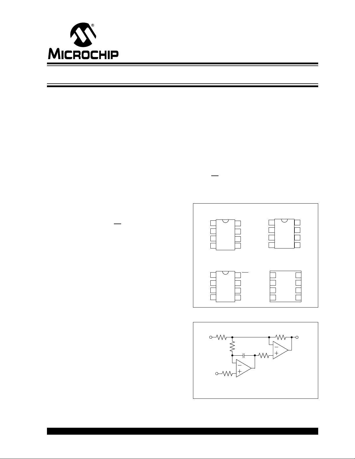
MCP6V06
SOIC
MCP6V07
SOIC
VIN+
V
IN
–
V
SS
V
DD
V
OUT
1
2
3
4
8
7
6
5
NC
CS
NC
MCP6V08
SOIC
V
INA
+
V
INA
–
V
SS
1
2
3
4
8
7
6
5
V
OUTA
V
DD
V
OUTB
V
INB
–
V
INB
+
MCP6V07
4×4 DFN
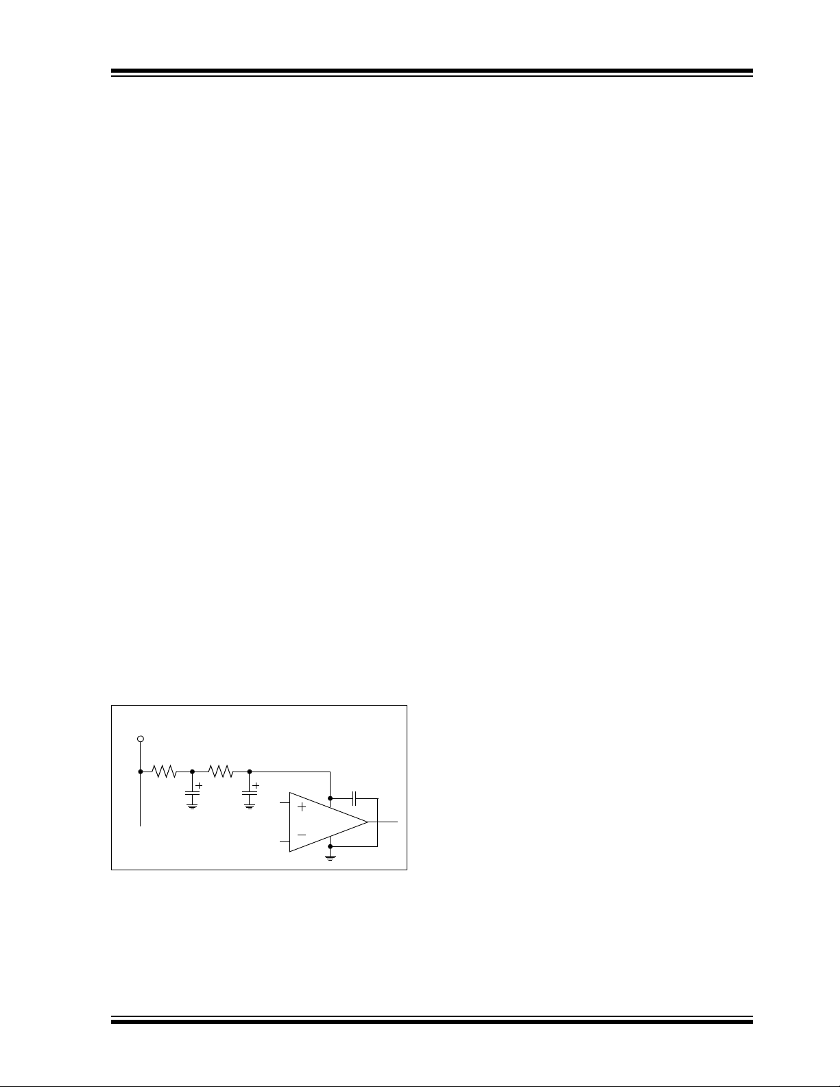
Offset Voltage Correction for Power Driver
MCP6V06
C
2
R
2
R
1
R
3
MCP6XXX
VDD/2
3kΩ
V
IN
V
OUT
R
2
300 µA, Auto-Zeroed Op Amps
Features
• High DC Precision:
-VOS Drift: ±50 nV/°C (maximum)
: ±3 µV (maximum)
-V
OS
: 125 dB (minimum)
-A
OL
- PSRR: 125 dB (minimum)
- CMRR: 120 dB (minimum)
-E
: 1.7 µV
ni
(typical), f = 0.1 Hz to 10 Hz
P-P
-Eni: 0.54 µVp-p (typical), f = 0.01 Hz to 1 Hz
• Low Power and Supply Voltages:
: 300 µA/amplifier (typical)
-I
Q
- Wide Supply Voltage Range: 1.8V to 5.5V
• Easy to Use:
- Rail-to-Rail Input/Output
- Gain Bandwidth Product: 1.3 MHz (typical)
- Unity Gain Stable
- Available in Single and Dual
- Single with Chip Select (CS
): MCP6V08
• Extended Temperature Range: -40°C to +125°C
Typical Applications
• Portable Instrumentation
• Sensor Conditioning
• Temperature Measurement
• DC Offset Correction
• Medical Instrumentation
Description
The Microchip Technology Inc. MCP6V06/7/8 family of
operational amplifiers has input offset voltage
correction for very low offset and offset drift. These
devices have a wide gain bandwidth product (1.3 MHz,
typical) and strongly reject switching noise. They are
unity gain stable, have no 1/f noise, and have good
PSRR and CMRR. These products operate with a
single supply voltage as low as 1.8V, while drawing
300 µA/amplifier (typical) of quiescent current.
The Microchip Technology Inc. MCP6V06/7/8 op amps
are offered in single (MCP6V06), single with Chip
Select (CS
) (MCP6V08), and dual (MCP6V07). They
are designed in an advanced CMOS process.
Package Types
Design Aids
• SPICE Macro Models
• FilterLab® Software
• Mindi™ Circuit Designer & Simulator
• Microchip Advanced Part Selector (MAPS)
• Analog Demonstration and Evaluation Boards
• Application Notes
Related Parts
• MCP6V01/2/3: Spread clock, lower offset
© 2008 Microchip Technology Inc. DS22093A-page 1
Typical Application Circuit
Page 2

MCP6V06/7/8
1.0 ELECTRICAL CHARACTERISTICS
1.1 Absolute Maximum Ratings †
VDD–VSS .......................................................................6.5V
Current at Input Pins ....................................................±2 mA
Analog Inputs (V
All other Inputs and Outputs ............ V
Difference Input voltage ...................................... |V
+ and VIN–) †† ... VSS– 1.0V to VDD+1.0V
IN
– 0.3V to VDD+0.3V
SS
DD–VSS
Output Short Circuit Current .................................Continuous
Current at Output and Supply Pins ............................±30 mA
Storage Temperature ....................................-65°C to +150°C
|
† Notice: Stresses above those listed under “Absolute
Maximum Ratings” may cause permanent damage to the
device. This is a stress rating only and functional operation of
the device at those or any other conditions above those
indicated in the operational listings of this specification is not
implied. Exposure to maximum rating conditions for extended
periods may affect device reliability.
†† See Section 4.2.1 “Rail-to-Rail Inputs”.
Max. Junction Temperature ........................................+150°C
ESD protection on all pins (HBM, MM) ................≥ 4 kV, 300V
1.2 Specifications
TABLE 1-1: DC ELECTRICAL SPECIFICATIONS
Electrical Characteristics: Unless otherwise indicated, TA = +25°C, VDD = +1.8V to +5.5V, VSS = GND, VCM = VDD/3,
V
OUT=VDD
Input Offset
Input Offset Voltage V
Input Offset Voltage Drift with Temperature
(linear Temp. Co.)
Input Offset Voltage Quadratic Temp. Co. TC
Power Supply Rejection PSRR 125 142 — dB (Note 1)
Input Bias Current and Impedance
Input Bias Current I
Input Bias Current across Temperature I
Input Offset Current I
Input Offset Current across Temperature I
Common Mode Input Impedance Z
Differential Input Impedance Z
Common Mode
Common-Mode Input Voltage Range V
Common-Mode Rejection CMRR 120 136 — dB V
Open-Loop Gain
DC Open-Loop Gain (large signal) A
Note 1: Set by design and characterization. Due to thermal junction and other effects in the production environment, these
/2, VL=VDD/2, RL = 20 kΩ to VL, and CS = GND (refer to Figure 1-5 and Figure 1-6).
Parameters Sym Min Typ Max Units Conditions
OS
TC
1
2
B
B
I
B
OS
OS
I
OS
CM
DIFF
CMRVSS
CMRR 130 147 — dB V
OL
A
OL
parts can only be screened in production (except TC
2: Figure 2-18 shows how V
changed across temperature for the first three production lots.
CMR
-3 — +3 µV TA = +25°C (Note 1)
-50 — +50 nV/°C TA = -40 to +125°C
(Note 1)
— ±0.15 — nV/°C2TA = -40 to +125°C
—+6—pA
—+140— pAT
= +85°C
A
— +1500 +5000 pA TA = +125°C
—-85— pA
—-85— pAT
= +85°C
A
-1000 -190 1000 pA TA = +125°C
—1013||6 — Ω||pF
—1013||6 — Ω||pF
− 0.20 — VDD+0.20 V (Note 2)
DD
V
CM
(Note 1, Note 2)
DD
V
CM
(Note 1, Note 2)
125 147 — dB VDD=1.8V,
V
OUT
135 158 — dB VDD=5.5V,
V
OUT
; see Appendix B: “Offset Related Test Screens”).
1
= 1.8V,
= -0.2V to 2.0V
= 5.5V,
= -0.2V to 5.7V
= 0.2V to 1.6V (Note 1)
= 0.2V to 5.3V (Note 1)
DS22093A-page 2 © 2008 Microchip Technology Inc.
Page 3

MCP6V06/7/8
TABLE 1-1: DC ELECTRICAL SPECIFICATIONS (CONTINUED)
Electrical Characteristics: Unless otherwise indicated, TA = +25°C, VDD = +1.8V to +5.5V, VSS = GND, VCM = VDD/3,
V
OUT=VDD
Output
Maximum Output Voltage Swing V
Output Short Circuit Current I
Power Supply
Supply Voltage V
Quiescent Current per amplifier I
POR Trip Voltage V
Note 1: Set by design and characterization. Due to thermal junction and other effects in the production environment, these
TABLE 1-2: AC ELECTRICAL SPECIFICATIONS
Electrical Characteristics: Unless otherwise indicated, TA = +25°C, VDD = +1.8V to +5.5V, VSS = GND, VCM = VDD/3,
V
OUT=VDD
Amplifier AC Response
Gain Bandwidth Product GBWP — 1.3 — MHz
Slew Rate SR — 0.5 — V/µs
Phase Margin PM — 65 — ° G = +1
Amplifier Noise Response
Input Noise Voltage E
Input Noise Voltage Density e
Input Noise Current Density i
Amplifier Distortion (Note 1)
Intermodulation Distortion (Not DC) IMD — 32 — µV
Amplifier Step Response
Start Up Time t
Offset Correction Settling Time t
Output Overdrive Recovery Time t
Note 1: These parameters were characterized using the circuit in Figure 1-7. Figure 2-37 and Figure 2-38 show both an IMD
/2, VL=VDD/2, RL = 20 kΩ to VL, and CS = GND (refer to Figure 1-5 and Figure 1-6).
Parameters Sym Min Typ Max Units Conditions
, V
OL
OHVSS
SC
I
SC
DD
Q
POR
parts can only be screened in production (except TC
2: Figure 2-18 shows how V
changed across temperature for the first three production lots.
CMR
/2, VL=VDD/2, RL = 20 kΩ to VL, CL = 60 pF, and CS = GND (refer to Figure 1-5 and Figure 1-6).
+15 — VDD− 15 mV G = +2, 0.5V input overdrive
—±7—mAVDD=1.8V
—±22— mAVDD=5.5V
1.8 — 5.5 V
200 300 400 µA IO = 0
1.15 — 1.65 V
; see Appendix B: “Offset Related Test Screens”).
1
Parameters Sym Min Typ Max Units Conditions
—0.54— µV
ni
—1.7—µV
E
ni
—82 —nV/√Hz f < 2.5 kHz
ni
—52 —nV/√Hz f = 100 kHz
e
ni
—0.6—fA/√Hz
ni
IMD — 25 — µV
—500— µs VOS within 50 µV of its final value
STR
— 300 — µs G = +1, VIN step of 2V,
STL
— 100 — µs G = -100, ±0.5V input overdrive to VDD/2,
ODR
tone at DC and a residual tone at1 kHz; all other IMD and clock tones are spread by the randomization circuitry.
2: t
includes some uncertainty due to clock edge timing.
ODR
f = 0.01 Hz to 1 Hz
P-P
f = 0.1 Hz to 10 Hz
P-P
PKVCM
PKVCM
tone = 50 mV
tone = 50 mV
V
within 50 µV of its final value
OS
V
50% point to V
IN
at 1 kHz, GN = 1, VDD = 5.5V
PK
at 1 kHz, GN = 1, VDD = 5.5V
PK
90% point (Note 2)
OUT
© 2008 Microchip Technology Inc. DS22093A-page 3
Page 4

MCP6V06/7/8
TABLE 1-3: DIGITAL ELECTRICAL SPECIFICATIONS
Electrical Characteristics: Unless otherwise indicated, TA = +25°C, VDD = +1.8V to +5.5V, VSS = GND, VCM = VDD/3,
V
OUT=VDD
CS Pull-Down Resistor (MCP6V08)
Pull-Down Resistor R
CS
Low Specifications (MCP6V08)
CS
Logic Threshold, Low V
CS
CS Input Current, Low I
CS High Specifications (MCP6V08)
Logic Threshold, High V
CS
CS Input Current, High I
CS Input High, GND Current per
amplifier
Amplifier Output Leakage, CS
CS Dynamic Specifications (MCP6V08)
Low to Amplifier Output On
CS
Turn-on Time
CS
High to Amplifier Output High-Z t
Internal Hysteresis V
/2, VL=VDD/2, RL = 20 kΩ to VL, CL = 60 pF, and CS = GND (refer to Figure 1-5 and Figure 1-6).
Parameters Sym Min Typ Max Units Conditions
35—MΩ
V
SS
—0.3VDDV
—5—pA
0.7V
DD
—VDD/R
—VDDV
—pA
PD
—-0.7—µA
—-2.3—µA
—20—pA
— 11 100 µs
—10—µs
—0.25—V
CS
= V
SS
CS
= V
DD
CS
= VDD, VDD = 1.8V
CS
= VDD, VDD = 5.5V
CS
= V
DD
CS
Low = VSS+0.3 V, G = +1 V/V,
= 0.9 VDD/2
V
OUT
CS
High = VDD– 0.3 V, G = +1 V/V,
= 0.1 VDD/2
V
OUT
High I
PD
IL
CSL
IH
CSH
I
SS
I
SS
O_LEAK
t
ON
OFF
HYST
TABLE 1-4: TEMPERATURE SPECIFICATIONS
Electrical Characteristics: Unless otherwise indicated, all limits are specified for: V
Parameters Sym Min Typ Max Units Conditions
Temperature Ranges
Specified Temperature Range T
Operating Temperature Range T
Storage Temperature Range T
-40 — +125 °C
A
-40 — +125 °C (Note 1)
A
-65 — +150 °C
A
Thermal Package Resistances
Thermal Resistance, 8L-4×4 DFN θ
Thermal Resistance, 8L-SOIC θ
Note 1: Operation must not cause T
J
JA
JA
to exceed Maximum Junction Temperature specification (150°C).
2: Measured on a standard JC51-7, four layer printed circuit board with ground plane and vias.
—44—°C/W(Note 2)
— 150 — °C/W
DD
= +1.8V to +5.5V, VSS = GND.
DS22093A-page 4 © 2008 Microchip Technology Inc.
Page 5

MCP6V06/7/8
V
DD
V
OS
VOS+50µV
V
OS
–50µV
t
STR
0V
1.8V to 5.5V
1.8V
V
IN
V
OS
VOS+50µV
VOS+50µV
t
STL
V
IN
V
OUT
V
DD
V
SS
t
ODR
t
ODR
VDD/2
V
IL
High-Z
t
ON
V
IH
CS
t
OFF
V
OUT
-2 µA
High-Z
I
SS
-2 µA
300 µA
1µA
I
DD
1µA
300 µA
VDD/5 MΩ
I
CS
VDD/5 MΩ
5pA
(typical)
(typical)
(typical) (typical)
(typical) (typical)
(typical)
(typical)
(typical)
V
DD
MCP6V0X
R
G
R
F
R
N
V
OUT
V
IN
VDD/3
1µF
C
L
R
L
V
L
100 nF
R
ISO
V
DD
MCP6V0X
R
G
R
F
R
N
V
OUT
VDD/3
V
IN
1µF
C
L
R
L
V
L
100 nF
R
ISO
V
DD
MCP6V0X
V
OUT
1µF
C
L
R
L
V
L
100 nF
R
ISO
20.0 kΩ
24.9 Ω
20.0 kΩ 50Ω
V
IN
V
REF
0.1%
0.1% 25 turn
20.0 kΩ
20.0 kΩ
0.1%
0.1%
2.49 kΩ 2.49 kΩ
1.3 Timing Diagrams
FIGURE 1-1: Amplifier Start Up.
FIGURE 1-2: Offset Correction Settling
Time.
1.4 Test Circuits
The circuits used for the DC and AC tests are shown in
Figure 1-5 and Figure 1-6. Lay the bypass capacitors
out as discussed in Section 4.3.7 “Supply Bypassing
and Filtering”. R
and RG to minimize bias current effects.
of R
F
FIGURE 1-5: AC and DC Test Circuit for Most Non-Inverting Gain Conditions.
is equal to the parallel combination
N
FIGURE 1-3: Output Overdrive Recovery.
FIGURE 1-4: Chip Select (MCP6V08).
© 2008 Microchip Technology Inc. DS22093A-page 5
FIGURE 1-6: AC and DC Test Circuit for Most Inverting Gain Conditions.
The circuit in Figure 1-7 tests the op amp input’s
dynamic behavior (i.e., IMD, t
potentiometer balances the resistor network (V
should equal V
at DC). The op amp’s common
REF
STR
, t
STL
and t
ODR
). The
OUT
mode input voltage is VCM=VIN/2. The error at the
input (V
) appears at V
ERR
with a noise gain of
OUT
10 V/V.
FIGURE 1-7: Test Circuit for Dynamic Input Behavior.
Page 6
MCP6V06/7/8
0%
2%
4%
6%
8%
10%
12%
14%
-2.0
-1.5
-1.0
-0.5
0.0
0.5
1.0
1.5
2.0
Input Offset Voltage (µV)
Percentage of Occurrences
80 Samples
T
A
= +25°C
V
DD
= 1.8V and 5.5V
Soldered on PCB
0%
5%
10%
15%
20%
25%
-50
-40
-30
-20
-10
0
10
20
30
40
50
Input Offset Voltage Drift; TC1 (nV/°C)
Percentage of Occurrences
80 Samples
V
DD
= 1.8V and 5.5V
Soldered on PCB
0%
5%
10%
15%
20%
25%
30%
-0.4
-0.2
0.0
0.2
0.4
Input Offset Voltage's Quadratic Temp Co;
TC
2
(nV/°C2)
Percentage of Occurrences
80 Samples
V
DD
= 1.8V and 5.5V
Soldered on PCB
-4
-3
-2
-1
0
1
2
3
4
0.00.51.01.52.02.53.03.54.04.55.05.56.06.5
Power Supply Voltage (V)
Input Offset Voltage (µV)
+125°C
+85°C
+25°C
-40°C
VCM = V
CMR_L
Representative Part
-4
-3
-2
-1
0
1
2
3
4
0.00.51.01.52.02.53.03.54.04.55.05.56.06.5
Power Supply Voltage (V)
Input Offset Voltage (µV)
+125°C
+85°C
+25°C
-40°C
VCM = V
CMR_H
Representative Part
-4
-3
-2
-1
0
1
2
3
4
0.00.51.01.52.02.53.03.54.04.55.05.5
Output Voltage (V)
Input Offset Voltage (µV)
VDD = 1.8V
VDD = 5.5V
Representative Part
2.0 TYPICAL PERFORMANCE CURVES
Note: The graphs and tables provided following this note are a statistical summary based on a limited number of
samples and are provided for informational purposes only. The performance characteristics listed herein
are not tested or guaranteed. In some graphs or tables, the data presented may be outside the specified
operating range (e.g., outside specified power supply range) and therefore outside the warranted range.
Note: Unless otherwise indicated, TA= +25°C, VDD= +1.8V to 5.5V, VSS= GND, VCM=VDD/3, V
V
L=VDD
/2, RL=20kΩ to VL, CL = 60 pF, and CS = GND.
2.1 DC Input Precision
FIGURE 2-1: Input Offset Voltage.
FIGURE 2-4: Input Offset Voltage vs.
Power Supply Voltage with V
OUT=VDD
/2,
CM=VCMR_L
.
FIGURE 2-2: Input Offset Voltage Drift.
FIGURE 2-3: Input Offset Voltage
Quadratic Temp Co.
DS22093A-page 6 © 2008 Microchip Technology Inc.
FIGURE 2-5: Input Offset Voltage vs.
Power Supply Voltage with V
CM=VCMR_H
.
FIGURE 2-6: Input Offset Voltage vs. Output Voltage.
Page 7

MCP6V06/7/8
-4
-3
-2
-1
0
1
2
3
4
-0.6
-0.4
-0.2
0.0
0.2
0.4
0.6
0.8
1.0
1.2
1.4
1.6
1.8
2.0
2.2
2.4
Input Common Mode Voltage (V)
Input Offset Voltage (µV)
VDD = 1.8V
Representative Part
-40°C
+25°C
+85°C
+125°C
-4
-3
-2
-1
0
1
2
3
4
-0.5
0.0
0.5
1.0
1.5
2.0
2.5
3.0
3.5
4.0
4.5
5.0
5.5
6.0
Input Common Mode Voltage (V)
Input Offset Voltage (µV)
VDD = 5.5V
Representative Part
0%
5%
10%
15%
20%
25%
30%
35%
-0.4
-0.3
-0.2
-0.2
-0.1
0.0
0.1
0.2
0.2
0.3
0.4
1/CMRR (µV/V)
Percentage of Occurrences
39 Samples
T
A
= +25°C
Soldered on PCB
VDD = 1.8V
VDD = 5.5V
0%
2%
4%
6%
8%
10%
12%
14%
-0.4
-0.3
-0.2
-0.1
0.0
0.1
0.2
0.3
0.4
1/PSRR (µV/V)
Percentage of Occurrences
40 Samples
T
A
= +25°C
Soldered on PCB
0%
5%
10%
15%
20%
25%
30%
35%
40%
45%
50%
-0.3
-0.2
-0.1
0.0
0.1
0.2
0.3
1/AOL (µV/V)
Percentage of Occurrences
40 Samples
T
A
= +25°C
Soldered on PCB
VDD = 1.8V
VDD = 5.5V
120
125
130
135
140
145
150
155
160
-50 -25 0 25 50 75 100 125
Ambient Temperature (°C)
CMRR, PSRR (dB)
PSRR
CMRR
VDD = 5.5V
V
DD
= 1.8V
Note: Unless otherwise indicated, TA= +25°C, VDD= +1.8V to 5.5V, VSS= GND, VCM=VDD/3, V
V
L=VDD
FIGURE 2-7: Input Offset Voltage vs.
Common Mode Voltage with V
/2, RL=20kΩ to VL, CL = 60 pF, and CS = GND.
=1.8V.
DD
+125°C
+85°C
+25°C
-40°C
FIGURE 2-10: PSRR.
OUT=VDD
/2,
FIGURE 2-8: Input Offset Voltage vs.
Common Mode Voltage with V
FIGURE 2-9: CMRR.
© 2008 Microchip Technology Inc. DS22093A-page 7
FIGURE 2-11: DC Open-Loop Gain.
=5.5V.
DD
FIGURE 2-12: CMRR and PSRR vs. Ambient Temperature.
Page 8

MCP6V06/7/8
120
125
130
135
140
145
150
155
160
-50 -25 0 25 50 75 100 125
Ambient Temperature (°C)
DC Open-Loop Gain (dB)
VDD = 5.5V
V
DD
= 1.8V
-150
-100
-50
0
50
100
150
200
-0.5
0.0
0.5
1.0
1.5
2.0
2.5
3.0
3.5
4.0
4.5
5.0
5.5
6.0
Common Mode Input Voltage (V)
Input Bias, Offset Currents
(pA)
I
B
TA = +85°C
DD
= 5.5V
I
OS
-400
-200
0
200
400
600
800
1000
1200
1400
1600
-0.5
0.0
0.5
1.0
1.5
2.0
2.5
3.0
3.5
4.0
4.5
5.0
5.5
6.0
Common Mode Input Voltage (V)
Input Bias, Offset Currents
(pA)
I
B
TA = +125°C
V
DD
= 5.5V
I
OS
1
10
100
1,000
10,000
25 35 45 55 65 75 85 95 105 115 125
Ambient Temperature (°C)
Input Bias, Offset Currents
(pA)
VDD = 5.5V
-I
OS
I
B
1.E-12
1.E-11
1.E-10
1.E-09
1.E-08
1.E-07
1.E-06
1.E-05
1.E-04
1.E-03
1.E-02
-1.0 -0.9 -0.8 -0.7 -0.6 -0.5 -0.4 -0.3 -0.2 -0.1 0.0
Input Voltage (V)
Input Current Magnitude (A)
+125°C
+85°C
+25°C
10m
1m
100µ
10µ
1µ
100n
10n
1n
100p
10p
1p
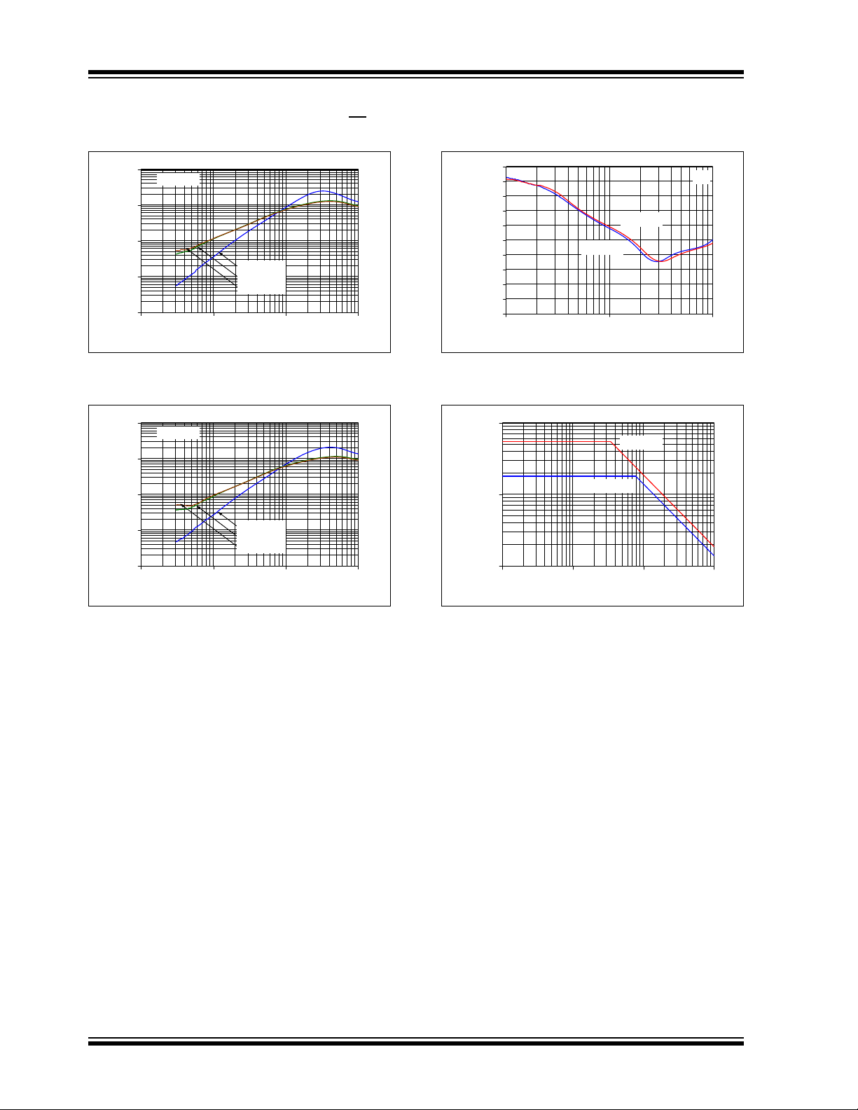
Note: Unless otherwise indicated, TA= +25°C, VDD= +1.8V to 5.5V, VSS= GND, VCM=VDD/3, V
V
L=VDD
FIGURE 2-13: DC Open-Loop Gain vs. Ambient Temperature.
/2, RL=20kΩ to VL, CL = 60 pF, and CS = GND.
V
FIGURE 2-16: Input Bias and Offset
Currents vs. Ambient Temperature with
V
= +5.5V.
DD
OUT=VDD
/2,
FIGURE 2-14: Input Bias and Offset
Currents vs. Common Mode Input Voltage with
T
=+85°C.
A
FIGURE 2-15: Input Bias and Offset
Currents vs. Common Mode Input Voltage with
T
= +125°C.
A
DS22093A-page 8 © 2008 Microchip Technology Inc.
-40°C
FIGURE 2-17: Input Bias Current vs. Input
Voltage (below V
SS
).
Page 9

MCP6V06/7/8
-0.35
-0.30
-0.25
-0.20
-0.15
-0.10
-0.05
0.00
0.05
-50 -25 0 25 50 75 100 125
Ambient Temperature (°C)
Input Common Mode Voltage
Headroom (V)
Lower (V
CMR
– VSS)
Upper ( VDD – V
CMR
)
3 Lots
10
100
1000
0.1 1 10
Output Current Magnitude (mA)
Output Voltage Headroom
(mV)
VDD – V
V
DD
VOL – V
V
DD
V
0
1
2
3
4
5
6
7
8
9
10
11
12
-50 -25 0 25 50 75 100 125
Ambient Temperature (°C)
Output Headroom (mV)
VDD – V
V
DD
VOL – V
SS
V
DD
RL = 20 k
-40
-30
-20
-10
0
10
20
30
40
0.0
0.5
1.0
1.5
2.0
2.5
3.0
3.5
4.0
4.5
5.0
5.5
6.0
6.5
Power Supply Voltage (V)
Output Short Circuit Current
(mA)
-40°C
+25°C
+85°C
+125°C
+125°C
+85°C
+25°C
-40°C
0
50
100
150
200
250
300
350
400
450
0.0
0.5
1.0
1.5
2.0
2.5
3.0
3.5
4.0
4.5
5.0
5.5
6.0
6.5
Power Supply Voltage (V)
Supply Current (µA)
-40°C
0%
5%
10%
15%
20%
25%
30%
1.1
1.2
1.3
1.4
1.5
1.6
1.7
POR Trip Voltage (V)
Percentage of Occurrences
93 Samples
3 Lots
T
A
= +25°C
Note: Unless otherwise indicated, TA= +25°C, VDD= +1.8V to 5.5V, VSS= GND, VCM=VDD/3, V
V
L=VDD
/2, RL=20kΩ to VL, CL = 60 pF, and CS = GND.
2.2 Other DC Voltages and Currents
FIGURE 2-18: Input Common Mode Voltage Headroom (Range) vs. Ambient Temperature.
= 5.5V
FIGURE 2-21: Output Short Circuit Current vs. Power Supply Voltage.
OUT=VDD
/2,
OH
FIGURE 2-19: Output Voltage Headroom vs. Output Current.
Ω
= 5.5V
= 1.8V
FIGURE 2-20: Output Voltage Headroom vs. Ambient Temperature.
© 2008 Microchip Technology Inc. DS22093A-page 9
= 1.8
+125°C
+85°C
+25°C
SS
FIGURE 2-22: Supply Current vs. Power Supply Voltage.
OH
FIGURE 2-23: Power On Reset Trip Voltage.
Page 10

MCP6V06/7/8
0.0
0.2
0.4
0.6
0.8
1.0
1.2
1.4
1.6
1.8
-50 -25 0 25 50 75 100 125
Ambient Temperature (°C)
POR Trip Voltage (V)
Note: Unless otherwise indicated, TA= +25°C, VDD= +1.8V to 5.5V, VSS= GND, VCM=VDD/3, V
V
L=VDD
/2, RL=20kΩ to VL, CL = 60 pF, and CS = GND.
FIGURE 2-24: Power On Reset Voltage vs. Ambient Temperature.
OUT=VDD
/2,
DS22093A-page 10 © 2008 Microchip Technology Inc.
Page 11

MCP6V06/7/8
0
10
20
30
40
50
60
70
80
90
100
110
1.E+01 1.E+02 1.E+03 1.E+04 1.E+05 1.E+06
Frequency (Hz)
CMRR, PSRR (dB)
CMRR
PSRR+
PSRR-
10 100k1k 1M10k100
-30
-20
-10
0
10
20
30
40
50
60
1.E+03 1.E+04 1.E+05 1.E+06 1.E+07
Frequency (Hz)
Open-Loop Gain (dB)
-270
-240
-210
-180
-150
-120
-90
-60
-30
0
Open-Loop Phase (°)
| AOL |
∠
A
OL
1k 10k 100k 1M 10M
VDD = 1.8V
C
L
= 60 pF
-30
-20
-10
0
10
20
30
40
50
60
1.E+03 1.E+04 1.E+05 1.E+06 1.E+07
Frequency (Hz)
Open-Loop Gain (dB)
-270
-240
-210
-180
-150
-120
-90
-60
-30
0
Open-Loop Phase (°)
| AOL |
∠
A
OL
1k 10k 100k 1M 10M
VDD = 5.5V
C
L
= 60 pF
0.0
0.2
0.4
0.6
0.8
1.0
1.2
1.4
1.6
1.8
-50 -25 0 25 50 75 100 125
Ambient Temperature (°C)
(MHz)
40
50
60
70
80
90
100
110
120
130
Phase Margin (°)
V
DD
PM
GBWP
DD
= 1.8V
0.0
0.2
0.4
0.6
0.8
1.0
1.2
1.4
1.6
1.8
-0.5
0.0
0.5
1.0
1.5
2.0
2.5
3.0
3.5
4.0
4.5
5.0
5.5
6.0
Common Mode Input Voltage (V)
Gain Bandwidth Product
(MHz)
40
50
60
70
80
90
100
110
120
130
Phase Margin (°)
V
DD
V
DD
GBWP
0.0
0.2
0.4
0.6
0.8
1.0
1.2
1.4
1.6
1.8
0.0 0.5 1.0 1.5 2.0 2.5 3.0 3.5 4.0 4.5 5.0 5.5
Output Voltage (V)
Gain Bandwidth Product
(MHz)
40
50
60
70
80
90
100
110
120
130
Phase Margin (°)
V
DD
V
PM
V
DD
GBWP
Note: Unless otherwise indicated, TA= +25°C, VDD= +1.8V to 5.5V, VSS= GND, VCM=VDD/3, V
V
L=VDD
/2, RL=20kΩ to VL, CL = 60 pF, and CS = GND.
2.3 Frequency Response
V
= 1.8V
FIGURE 2-25: CMRR and PSRR vs. Frequency.
Gain Bandwidth Product
FIGURE 2-28: Gain Bandwidth Product and Phase Margin vs. Ambient Temperature.
OUT=VDD
= 5.5V
= 5.5V
/2,
FIGURE 2-26: Open-Loop Gain vs.
Frequency with V
FIGURE 2-27: Open-Loop Gain vs.
Frequency with V
© 2008 Microchip Technology Inc. DS22093A-page 11
=1.8V.
DD
=5.5V.
DD
PM
FIGURE 2-29: Gain Bandwidth Product and Phase Margin vs. Common Mode Input Voltage.
= 1.8V
= 5.5
FIGURE 2-30: Gain Bandwidth Product and Phase Margin vs. Output Voltage.
Page 12
MCP6V06/7/8
1.E+00
1.E+01
1.E+02
1.E+03
1.E+04
1.0E+05 1.0E+06 1.0E+07 1.0E+08
Frequency (Hz)
VDD = 1.8V
100k 1M 10M 100M
1
10
100
1k
10k
G = 1 V/V
G = 10 V/V
G = 100 V/V
Open-Loop Output Impedance ( Ω )
1.E+00
1.E+01
1.E+02
1.E+03
1.E+04
1.0E+05 1.0E+06 1.0E+07 1.0E+08
Frequency (Hz)
VDD = 5.5V
100k 1M 10M 100M
1
10
100
1k
10k
G = 1 V/V
G = 10 V/V
G = 100 V/V
Open-Loop Output Impedance ( Ω )
0
10
20
30
40
50
60
70
80
90
100
1.E+05 1.E+06 1.E+07
Frequency (Hz)
Channel-to-Channel
Separation (dB)
V
DD
V
DD
100k 1M 10M
0.1
1
10
1.E+03 1.E+04 1.E+05 1.E+06
Frequency (Hz)
Maximum Output Voltage
Swing (V
P-P
)
V
DD
V
DD
1k 10k 100k 1M
Note: Unless otherwise indicated, TA= +25°C, VDD= +1.8V to 5.5V, VSS= GND, VCM=VDD/3, V
V
L=VDD
FIGURE 2-31: Closed-Loop Output
Impedance vs. Frequency with V
/2, RL=20kΩ to VL, CL = 60 pF, and CS = GND.
=1.8V.
DD
= 1.8V
FIGURE 2-33: Channel-to-Channel Separation vs. Frequency.
= 1.8V
OUT=VDD
= 5.5V
= 5.5V
/2,
RTI
FIGURE 2-32: Closed-Loop Output
Impedance vs. Frequency with V
DS22093A-page 12 © 2008 Microchip Technology Inc.
DD
=5.5V.
FIGURE 2-34: Maximum Output Voltage Swing vs. Frequency.
Page 13

MCP6V06/7/8
10
100
1,000
10,000
1.E+01 1.E+02 1.E+03 1.E+04 1.E+05
Freque ncy (Hz)
10
100
1000
Input Noise Voltage;
E
ni
(µV
P-P
)
10 1k 10k
e
ni
Eni(0 Hz to f)
e
ni
(nV/
√
Hz)
100
DD
= 5.5V
DD
= 1.8V
0
20
40
60
80
100
120
140
160
-0.5
0.0
0.5
1.0
1.5
2.0
2.5
3.0
3.5
4.0
4.5
5.0
5.5
6.0
Common Mode Input Voltage (V)
V
DD
V
V
DD
V
Input Noise Voltage Density;
e
ni
(nV/
√
Hz)
1
10
100
1.E+02 1.E+03 1.E+04 1.E+05
Frequency (Hz)
IMD Spectrum, RTI (µV
PK
)
GDM = 1 V/V
V
CM
tone = 50 mVPK, f = 1 kHz
100 1k 10k 100k
IMD tone at DC
residual
1 kHz
tone
VDD = 5.5V
V
DD
= 1.8V
1
10
100
1.E+02 1.E+03 1.E+04 1.E+05
Frequency (Hz)
IMD Spectrum, RTI (µV
PK
)
100 1k 10k 100k
GDM = 1 V/V
V
DD
tone = 50 mVPK, f = 1 kHz
IMD tone at DC
1 kHz
tone
VDD = 5.5V
V
DD
= 1.8V
0 102030405060708090100
t (s)
Input Noise Voltage; e
ni
(t)
(0.5 µV/div)
VDD = 1.8V
NPBW = 10 Hz
NPBW = 1 Hz
0 102030405060708090100
t (s)
Input Noise Voltage; e
ni
(t)
(0.5 µV/div)
VDD = 5.5V
NPBW = 10 Hz
NPBW = 1 Hz
Note: Unless otherwise indicated, TA= +25°C, VDD= +1.8V to 5.5V, VSS= GND, VCM=VDD/3, V
VL=VDD/2, RL=20kΩ to VL, CL = 60 pF, and CS = GND.
2.4 Input Noise and Distortion
V
V
Input Noise Voltage Density;
FIGURE 2-35: Input Noise Voltage Density vs. Frequency.
100k
= 5.5
FIGURE 2-38: Inter-Modulation Distortion
vs. Frequency with V
Disturbance (see
DD
Figure 1-7).
OUT=VDD
/2,
= 1.8
FIGURE 2-36: Input Noise Voltage Density vs. Input Common Mode Voltage.
FIGURE 2-37: Inter-Modulation Distortion
vs. Frequency with V
Figure 1-7).
© 2008 Microchip Technology Inc. DS22093A-page 13
Disturbance (see
CM
FIGURE 2-39: Input Noise vs. Time with
1 Hz and 10 Hz Filters and V
DD
=1.8V.
FIGURE 2-40: Input Noise vs. Time with
1 Hz and 10 Hz Filters and V
DD
=5.5V.
Page 14

MCP6V06/7/8
-6
-5
-4
-3
-2
-1
0
1
2
3
4
5
6
7
0 20 40 60 80 100 120 140 160 180 200
Time (s)
Input Offset Voltage (µV)
-15
-10
-5
0
5
10
15
20
25
30
35
40
45
50
PCB Temperature (°C)
T
PCB
V
OS
Temperature increased by
using heat gun for 4 seconds.
-25
-20
-15
-10
-5
0
5
10
15
20
25
0.0 0.2 0.4 0.6 0.8 1.0 1.2 1.4 1.6 1.8 2.0Time (200 µs/div)
Input Offset Voltage
(mV)
0.0
0.5
1.0
1.5
2.0
2.5
3.0
3.5
4.0
4.5
5.0
Power Supply Voltage
(V)
POR Trip
Point
V
OS
V
DD
-1
0
1
2
3
4
5
6
7
012345678910
Time (ms)
Input, Output Voltages (V)
VDD = 5.5V
G = 1
V
V
02468101214161820
Time (µs)
Output Voltage (10 mV/div)
VDD = 5.5V
G = 1
0.0
0.5
1.0
1.5
2.0
2.5
3.0
3.5
4.0
4.5
5.0
5.5
0 5 10 15 20 25 30 35 40 45 50
Time (µs)
Output Voltage (V)
VDD = 5.5V
G = 1
012345678910
Time (µs)
Output Voltage (10 mV/div)
VDD = 5.5V
G = -1
Note: Unless otherwise indicated, TA= +25°C, VDD= +1.8V to 5.5V, VSS= GND, VCM=VDD/3, V
V
L=VDD
/2, RL=20kΩ to VL, CL = 60 pF, and CS = GND.
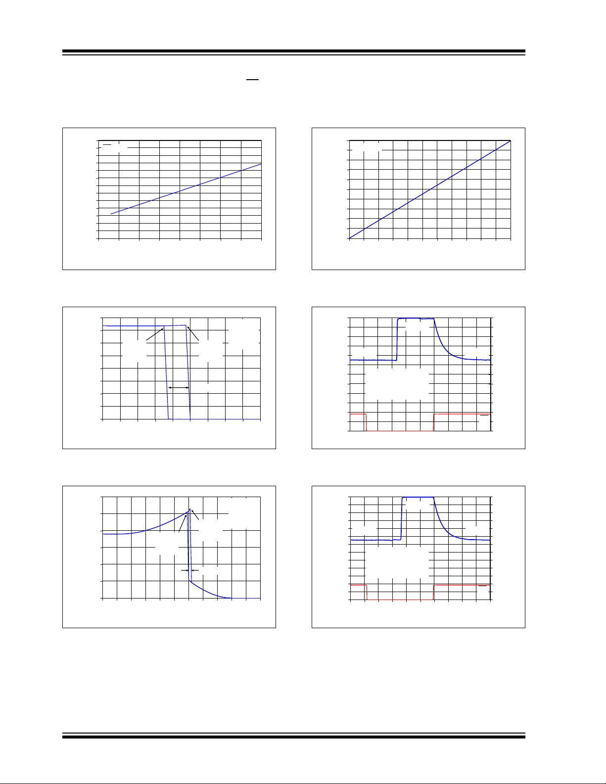
2.5 Time Response
FIGURE 2-41: Input Offset Voltage vs. Time with Temperature Change.
FIGURE 2-44: Non-inverting Small Signal Step Response.
OUT=VDD
/2,
FIGURE 2-42: Input Offset Voltage vs. Time at Power Up.
IN
OUT
FIGURE 2-43: The MCP6V06/7/8 family shows no input phase reversal with overdrive.
DS22093A-page 14 © 2008 Microchip Technology Inc.
FIGURE 2-45: Non-inverting Large Signal Step Response.
FIGURE 2-46: Inverting Small Signal Step Response.
Page 15

MCP6V06/7/8
0.0
0.5
1.0
1.5
2.0
2.5
3.0
3.5
4.0
4.5
5.0
5.5
0 5 10 15 20 25 30 35 40 45 50
Time (µs)
Output Voltage (V)
DD
= 5.5V
G = -1
0.0
0.1
0.2
0.3
0.4
0.5
0.6
0.7
0.8
0.9
-50 -25 0 25 50 75 100 125
Ambient Temperature (°C)
Slew Rate (V/µs)
Falling Edge
DD
= 5.5V
DD
= 1.8V
Rising Edge
-1.0
0.0
1.0
2.0
3.0
4.0
5.0
6.0
Time (50 µs/div)
Output Voltage (V)
-1
0
1
2
3
4
5
6
Input Voltage × G (V/V)
VDD = 5.5V
G = -100 V/V
0.5V Overdrive
V
OUT
G V
IN
V
OUT
G V
IN
1
10
100
1000
1 10 100 1000
Inverting Gain Magnitude (V/V)
Overdrive Recovery Time (µs)
0.5V Output Overdrive
t
ODR
, low
t
ODR
, high
DD
= 1.8V
DD
= 5.5V
Note: Unless otherwise indicated, TA= +25°C, VDD= +1.8V to 5.5V, VSS= GND, VCM=VDD/3, V
V
L=VDD
FIGURE 2-47: Inverting Large Signal Step Response.
/2, RL=20kΩ to VL, CL = 60 pF, and CS = GND.
V
FIGURE 2-49: Output Overdrive Recovery vs. Time with G = -100 V/V.
V
V
V
OUT=VDD
/2,
FIGURE 2-48: Slew Rate vs. Ambient Temperature.
© 2008 Microchip Technology Inc. DS22093A-page 15
V
FIGURE 2-50: Output Overdrive Recovery Time vs. Inverting Gain.
Page 16
MCP6V06/7/8
0.0
0.1
0.2
0.3
0.4
0.5
0.6
0.7
0.8
0.9
1.0
1.1
1.2
1.3
1.5 2.0 2.5 3.0 3.5 4.0 4.5 5.0 5.5
Power Supply Voltage (V)
Chip Select Current (µA)
CS = V
DD
0
50
100
150
200
250
300
350
400
0.0 0.2 0.4 0.6 0.8 1.0 1.2 1.4 1.6 1.8
Chip Select Voltage (V)
Power Supply Current (µA)
VDD = 1.8V
G = 1
V
IN
= 0.9V
V
L
= 0V
Hysteresis
Op Amp
turns on
here
Op Amp
turns off
here
0
100
200
300
400
500
600
0.00.51.01.52.02.53.03.54.04.55.05.5
Chip Select Voltage (V)
Power Supply Current (µA)
VDD = 5.5V
G = 1
V
IN
= 2.75V
V
L
= 0V
Hysteresis
Op Amp
turns on
here
Op Amp
turns off
here
0.0
0.1
0.2
0.3
0.4
0.5
0.6
0.7
0.8
0.9
1.0
0.0 0.5 1.0 1.5 2.0 2.5 3.0 3.5 4.0 4.5 5.0 5.5
Chip Select Voltage (V)
Chip Select Current (µA)
DD
= 5.5V
-0.6
-0.4
-0.2
0.0
0.2
0.4
0.6
0.8
1.0
1.2
1.4
1.6
1.8
Time (5 µs/div)
Output Voltage (V)
0
1
2
3
4
5
6
7
8
9
10
11
12
Chip Select Voltage (V)
VDD = 1.8V
G = +1 V/V
V
IN
= V
DD
RL = 10 kΩ tied to VDD/2
CS
V
OUT
On
V
OUT
OffV
OUT
Off
-1.0
-0.5
0.0
0.5
1.0
1.5
2.0
2.5
3.0
3.5
4.0
4.5
5.0
5.5
0 5 10 15 20 25 30 35 40 45 50
Time (5 µs/div)
Output Voltage (V)
0
3
6
9
12
15
18
21
24
27
30
33
36
39
Chip Select Voltage (V)
VDD = 5.5V
G = +1 V/V
V
IN
= V
DD
RL = 10 kΩ tied to VDD/2
CS
V
OUT
On
V
OUT
OffV
OUT
Off
Note: Unless otherwise indicated, TA= +25°C, VDD= +1.8V to 5.5V, VSS= GND, VCM=VDD/3, V
VL=VDD/2, RL=20kΩ to VL, CL = 60 pF, and CS = GND.
2.6 Chip Select Response (MCP6V08 only)
V
FIGURE 2-51: Chip Select Current vs. Power Supply Voltage.
FIGURE 2-54: Chip Select Current vs. Chip Select Voltage.
OUT=VDD
/2,
FIGURE 2-52: Power Supply Current vs.
Chip Select Voltage with V
FIGURE 2-53: Power Supply Current vs.
Chip Select Voltage with V
DS22093A-page 16 © 2008 Microchip Technology Inc.
DD
DD
=1.8V.
=5.5V.
FIGURE 2-55: Chip Select Voltage, Output
Voltage vs. Time with V
DD
=1.8V.
FIGURE 2-56: Chip Select Voltage, Output
Voltage vs. Time with V
DD
=5.5V.
Page 17
MCP6V06/7/8
30%
35%
40%
45%
50%
55%
60%
65%
70%
-50-25 0 255075100125
Ambient Temperature (°C)
Relative Chip Select Logic
Levels; Low and High ( )
VIL/V
DD
VIH/V
DD
VDD = 1.8V
VDD = 5.5V
0.00
0.05
0.10
0.15
0.20
0.25
0.30
0.35
0.40
-50 -25 0 25 50 75 100 125
Ambient Temperature (°C)
Chip Select Hysteresis (V)
VDD = 1.8V
VDD = 5.5V
0
2
4
6
8
10
12
14
16
-50 -25 0 25 50 75 100 125
Ambient Temperature (°C)
Chip Select Turn On Time
(µs)
DD
= 5.5V
DD
= 1.8V
0
1
2
3
4
5
6
7
-50 -25 0 25 50 75 100 125
Ambient Temperature (°C)
Pull-down Resistor (MΩ
0.0
0.2
0.4
0.6
0.8
1.0
1.2
1.4
1.6
1.8
2.0
0.0
0.5
1.0
1.5
2.0
2.5
3.0
3.5
4.0
4.5
5.0
5.5
6.0
6.5
Power Supply Voltage (V)
Power Supply Current (µA)
DD
t
Note: Unless otherwise indicated, TA= +25°C, VDD= +1.8V to 5.5V, VSS= GND, VCM=VDD/3, V
V
L=VDD
FIGURE 2-57: Chip Select Relative Logic Thresholds vs. Ambient Temperature.
/2, RL=20kΩ to VL, CL = 60 pF, and CS = GND.
)
FIGURE 2-60: Chip Select’s Pull-down
Resistor (R
) vs. Ambient Temperature.
PD
CS = V
Representative Par
+125°C
+85°C
+25°C
-40°C
OUT=VDD
/2,
FIGURE 2-58: Chip Select Hysteresis.
FIGURE 2-59: Chip Select Turn On Time
vs. Ambient Temperature.
© 2008 Microchip Technology Inc. DS22093A-page 17
FIGURE 2-61: Quiescent Current in Shutdown vs. Power Supply Voltage.
V
V
Page 18
MCP6V06/7/8
3.0 PIN DESCRIPTIONS
Descriptions of the pins are listed in Table 3-1.
TABLE 3-1: PIN FUNCTION TABLE
MCP6V06 MCP6V07 MCP6V08
SOIC DFN, SOIC SOIC
616V
222V
333V
444VSSNegative Power Supply
—5—V
—6—V
—7—V
787V
—— 8 CS
1, 5, 8 — 1, 5 NC No Internal Connection
Symbol Description
, V
OUT
OUTA
–, V
IN
INA
+, V
IN
INA
+ Non-inverting Input (op amp B)
INB
– Inverting Input (op amp B)
INB
OUTB
DD
Output (op amp A)
– Inverting Input (op amp A)
+ Non-inverting Input (op amp A)
Output (op amp B)
Positive Power Supply
Chip Select (op amp A)
3.1 Analog Outputs
The analog output pins (V
voltage sources.
) are low-impedance
OUT
3.2 Analog Inputs
The non-inverting and inverting inputs (VIN+, VIN–, …)
are high-impedance CMOS inputs with low bias
currents.
3.3 Power Supply Pins
The positive power supply (VDD) is 1.8V to 5.5V higher
than the negative power supply (VSS). For normal
operation, the other pins are between VSS and VDD.
Typically, these parts are used in a single (positive)
supply configuration. In this case, V
ground and VDD is connected to the supply. VDD will
need bypass capacitors.
is connected to
SS
3.4 Chip Select (CS) Digital Input
This pin (CS) is a CMOS, Schmitt-triggered input that
places the MCP6V08 op amps into a low power mode
of operation.
DS22093A-page 18 © 2008 Microchip Technology Inc.
Page 19

MCP6V06/7/8
VIN+
V
IN
–
Main
Output
V
OUT
V
REF
Amp.
Buffer
NC
Null
Amp.
Null
Input
φ
1
Switches
Null
Correct
φ
2
Switches
Null
Output
Switches
C
H
C
FW
POR
Digital
Control
Oscillator
CS
Clock
Randomization
φ
1
φ
2
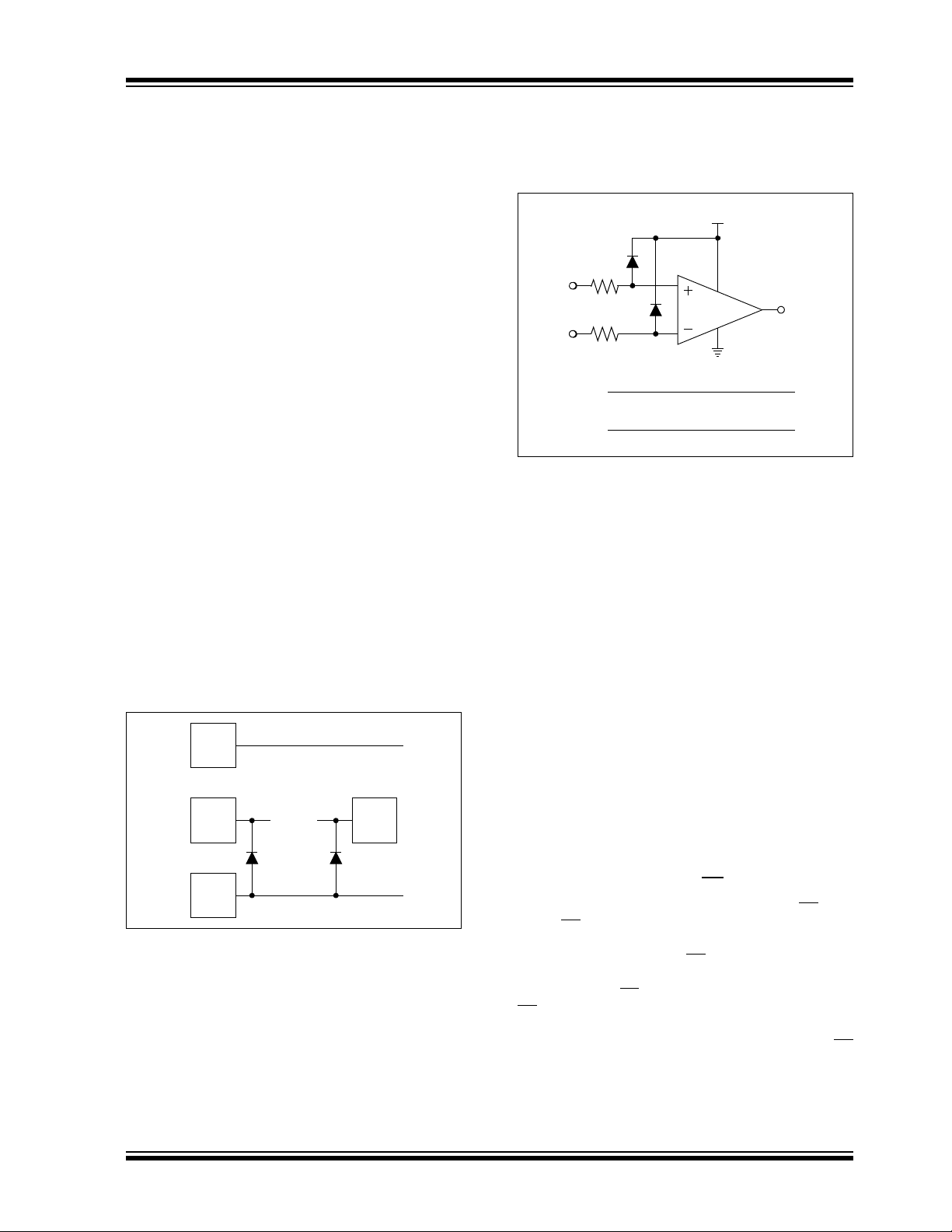
4.0 APPLICATIONS
The MCP6V06/7/8 family of auto-zeroed op amps is
manufactured using Microchip’s state of the art CMOS
process. It is designed for low cost, low power and high
precision applications. Its low supply voltage, low
quiescent current and wide bandwidth makes the
MCP6V06/7/8 ideal for battery-powered applications.
4.1 Overview of Auto-zeroing Operation
Figure 4-1 shows a simplified diagram of the
MCP6V06/7/8 auto-zeroed op amps. This will be used
to explain how the DC voltage errors are reduced in this
architecture.
FIGURE 4-1: Simplified Auto-zeroed Op Amp Functional Diagram.
4.1.1 BUILDING BLOCKS
The Null Amp. and Main Amp. are designed for high
FW
gain and accuracy using a differential topology. They
have an auxiliary input (bottom left) used for correcting
the offset voltages. Both inputs are added together
internally. The capacitors at the auxiliary inputs (C
and CH) hold the corrected values during normal
operation.
The Output Buffer is designed to drive external loads at
the V
OUT
voltage (V
pin. It also produces a single ended output
is an internal reference voltage).
REF
All of these switches are make-before-break in order to
minimize glitch-induced errors. They are driven by two
clock phases (φ
mode and auto-zeroing mode.
and φ2) that select between normal
1
The clock is derived from an internal R-C oscillator
running at a rate of f
output is divided down to the desired rate. It is also
randomized to minimize (spread) undesired clock
tones in the output.
© 2008 Microchip Technology Inc. DS22093A-page 19
= 650 kHz. The oscillator’s
OSC1
The internal POR ensures the part starts up in a known
good state. It also provides protection against power
supply brown out events.
The Chip Select input places the op amp in a low power
state when it is high. When it goes low, it powers the op
amp at its normal level and starts operation properly.
The Digital Control circuitry takes care of all of the
housekeeping details of the switching operation. It also
takes care of Chip Select and POR events.
Page 20

MCP6V06/7/8
VIN+
V
IN
–
Main
Output
V
OUT
V
REF
Amp.
Buffer
NC
Null
Amp.
C
H
C
FW
VIN+
V
IN
–
Main
Output
V
OUT
V
REF
Amp.
Buffer
NC
Null
Amp.
C
H
C
FW
4.1.2 AUTO-ZEROING ACTION
Figure 4-2 shows the connections between amplifiers
during the Normal Mode of operation (φ
). The hold
1
capacitor (CH) corrects the Null Amplifier’s input offset.
Since the Null Amplifier has very high gain, it
dominates the signal seen by the Main Amplifier. This
greatly reduces the impact of the Main Amplifier’s input
FIGURE 4-2: Normal Mode of Operation (
Figure 4-3 shows the connections between amplifiers
during the Auto-zeroing Mode of operation (φ2). The
signal goes directly through the Main Amplifier, and the
flywheel capacitor (C
tion on the Main Amplifier’s offset.
The Null Amplifier uses its own high open loop gain to
drive the voltage across C
offset voltage is almost zero. Because the principal
input is connected to V
corrects the offset at the current common mode input
voltage (V
) and supply voltage (VDD). This makes
CM
the DC CMRR and PSRR very high also.
) maintains a constant correc-
FW
to the point where its input
H
+, the auto-zeroing action
IN
offset voltage on overall performance. Essentially, the
Null Amplifier and Main Amplifier behave as a regular
op amp with very high gain (AOL) and very low offset
voltage (V
φ
); Equivalent Amplifier Diagram.
1
OS
).
Since these corrections happen every 50 µs, or so, we
also minimize slow errors, including offset drift with
temperature (ΔV
/ΔTA), 1/f noise, and input offset
OS
aging.
FIGURE 4-3: Auto-zeroing Mode of Operation (
4.1.3 INTERMODULATION DISTORTION
(IMD)
The MCP6V06/7/8 op amps will show intermodulation
φ
); Equivalent Diagram.
2
frequencies. IMD distortion tones are generated about
all of the square wave clock’s harmonics. See
Figure 2-37 and Figure 2-38.
distortion (IMD), products when an AC signal is
present.
The signal and clock can be decomposed into sine
wave tones (Fourier series components). These tones
interact with the auto-zeroing circuitry’s non-linear
response to produce IMD tones at sum and difference
DS22093A-page 20 © 2008 Microchip Technology Inc.
Page 21
MCP6V06/7/8
Bond
Pad
Bond
Pad
Bond
Pad
V
DD
VIN+
V
SS
Input
Stage
Bond
Pad
VIN–
V
1
MCP6V0X
R
1
V
DD
D
1
R1>
VSS– (minimum expected V1)
2mA
V
OUT
R2>
VSS– (minimum expected V2)
2mA
V
2
R
2
D
2
4.2 Other Functional Blocks
4.2.1 RAIL-TO-RAIL INPUTS
The input stage of the MCP6V06/7/8 op amps uses two
differential CMOS input stages in parallel. One
operates at low common mode input voltage (V
which is approximately equal to VIN+ and VIN– in normal operation) and the other at high V
CM
topology, the input operates with VCM up to 0.2V past
either supply rail at +25°C (see Figure 2-18). The input
offset voltage (V
) is measured at VCM=VSS–0.2V
OS
and VDD+ 0.2V to ensure proper operation.
The transition between the input stages occurs when
≈ VDD– 0.9V (see Figure 2-7 and Figure 2-8). For
V
CM
the best distortion and gain linearity, with non-inverting
gains, avoid this region of operation.
4.2.1.1 Phase Reversal
The input devices are designed to not exhibit phase
inversion when the input pins exceed the supply
voltages. Figure 2-43 shows an input voltage
exceeding both supplies with no phase inversion.
4.2.1.2 Input Voltage and Current Limits
The ESD protection on the inputs can be depicted as
shown in Figure 4-4. This structure was chosen to
protect the input transistors, and to minimize input bias
current (I
when they try to go more than one diode drop below
V
SS
above VDD; their breakdown voltage is high enough to
allow normal operation, and low enough to bypass
quick ESD events within the specified limits.
). The input ESD diodes clamp the inputs
B
. They also clamp any voltages that go too far
CM
. With this
pins (V
+ and VIN–) from going too far above VDD, and
IN
dump any currents onto VDD. When implemented as
shown, resistors R1 and R2 also limit the current
through D
and D2.
1
,
FIGURE 4-5: Protecting the Analog Inputs.
It is also possible to connect the diodes to the left of the
resistor R
the diodes D1 and D2 need to be limited by some other
mechanism. The resistors then serve as in-rush current
limiters; the DC current into the input pins (V
VIN–) should be very small.
A significant amount of current can flow out of the
inputs (through the ESD diodes) when the common
mode voltage (V
Figure 2-17. Applications that are high impedance may
need to limit the usable voltage range.
and R2. In this case, the currents through
1
+ and
IN
) is below ground (VSS); see
CM
FIGURE 4-4: Simplified Analog Input ESD Structures.
In order to prevent damage and/or improper operation
of these amplifiers, the circuit must limit the currents
(and voltages) at the input pins (see Section 1.1
“Absolute Maximum Ratings †”). Figure 4-5 shows
the recommended approach to protecting these inputs.
The internal ESD diodes prevent the input pins (V
and V
resistors R
of the input pins. Diodes D1 and D2 prevent the input
© 2008 Microchip Technology Inc. DS22093A-page 21
–) from going too far below ground, and the
IN
and R2 limit the possible current drawn out
1
4.2.2 RAIL-TO-RAIL OUTPUT
The output voltage range of the MCP6V06/7/8
auto-zeroed op amps is V
V
+ 15 mV (maximum) when RL=20kΩ is
SS
connected to V
/2 and VDD= 5.5V. Refer to
DD
– 15 mV (minimum) and
DD
Figure 2-19 and Figure 2-20 for more information.
These op amps are designed to drive light loads; use
another amplifier to buffer the output from heavy loads.
4.2.3 CHIP SELECT (CS)
The single MCP6V08 has a Chip Select (CS) pin.
When CS
corresponding op amp drops to about 1 µA (typical),
and is pulled through the CS
happens, the amplifier is put into a high impedance
state. By pulling CS
CS pin is left floating, the internal pull-down resistor
(about 5 MΩ) will keep the part on. Figure 1-4 shows
the output voltage and supply current response to a CS
+
IN
pulse.
is pulled high, the supply current for the
pin to VSS. When this
low, the amplifier is enabled. If the
Page 22
MCP6V06/7/8
VOSTA() VOSTC1ΔTTC2ΔT
2
++=
Where:
ΔT=T
A
–25°C
V
OS(TA
) = input offset voltage at T
A
V
OS
= input offset voltage at +25°C
TC
1
= linear temperature coefficient
TC
2
= quadratic temperature
coefficient
R
ISO
C
L
V
OUT
MCP6V0X
10
100
1000
10000
1.E-12 1.E-11 1.E-10 1.E-09 1.E-08 1.E-07
C
L
(F)
Recommended R
ISO
(Ω)
1p 10p 100p 1n 10n 100n
10
100
1k
10k
GN < 2
GN = 5
G
N
= 10
4.3 Application Tips
4.3.1 INPUT OFFSET VOLTAGE OVER
TEMPERATURE
Table 1-1 gives both the linear and quadratic tempera-
ture coefficients (TC1 and TC2) of input offset voltage.
The input offset voltage, at any temperature in the
specified range, can be calculated as follows:
EQUATION 4-1:
4.3.2 DC GAIN PLOTS
Figure 2-9, Figure 2-10 and Figure 2-11 are histograms
of the reciprocals (in units of µV/V) of CMRR, PSRR
and A
input offset voltage (VOS) with a change in common
mode input voltage (V
and output voltage (V
The 1/A
the measurements are dominated by the op amp’s
input noise. The negative values shown represent
noise, not unstable behavior. We validate the op amps’
stability by making multiple measurements of V
instability would manifest itself as a greater unexplained variability in V
, respectively. They represent the change in
OL
), power supply voltage (VDD)
CM
).
OUT
histogram is centered near 0 µV/V because
OL
or as the railing of the output.
OS
OS
4.3.5 CAPACITIVE LOADS
Driving large capacitive loads can cause stability
problems for voltage feedback op amps. As the load
capacitance increases, the feedback loop’s phase
margin decreases and the closed-loop bandwidth is
reduced. This produces gain peaking in the frequency
response, with overshoot and ringing in the step
response. These auto-zeroed op amps have a different
output impedance than most op amps, due to their
unique topology.
When driving a capacitive load with these op amps, a
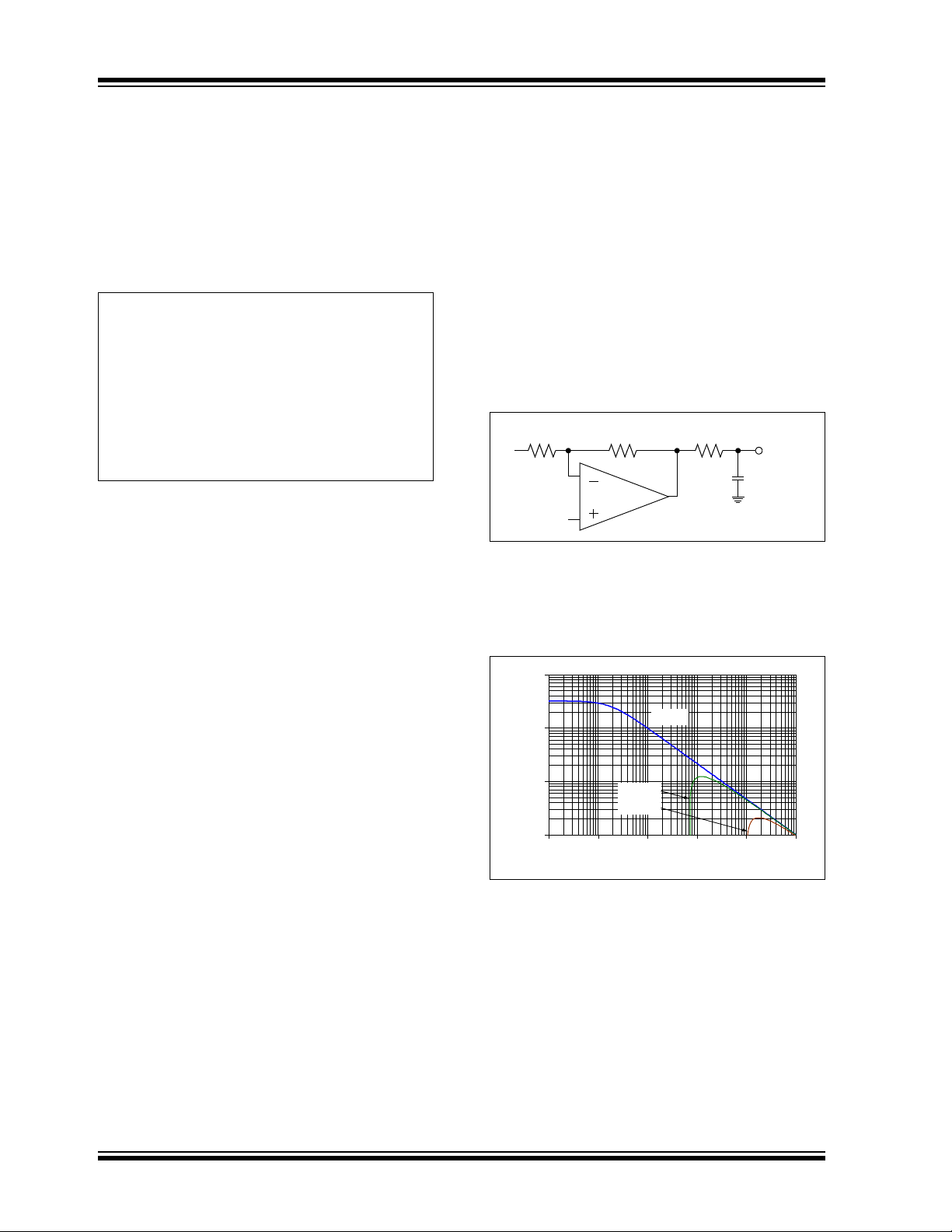
series resistor at the output (R
in Figure 4-6)
ISO
improves the feedback loop’s phase margin (stability)
by making the output load resistive at higher frequencies. The bandwidth will be generally lower than the
bandwidth with no capacitive load.
FIGURE 4-6: Output Resistor, R
ISO
,
Stabilizes Capacitive Loads.
Figure 4-7 gives recommended R
different capacitive loads and is independent of the
gain.
;
values for
ISO
4.3.3 SOURCE RESISTANCES
The input bias currents have two significant
components; switching glitches that dominate at room
temperature and below, and input ESD diode leakage
currents that dominate at +85°C and above.
Make the resistances seen by the inputs small and
equal. This minimizes the output offset caused by the
input bias currents.
The inputs should see a resistance on the order of 10Ω
to 1 kΩ at high frequencies (i.e., above 1 MHz). This
helps minimize the impact of switching glitches, which
are very fast, on overall performance. In some cases, it
may be necessary to add resistors in series with the
inputs to achieve this improvement in performance.
4.3.4 SOURCE CAPACITANCE
The capacitances seen by the two inputs should be
small and matched. The internal switches connected to
the inputs dump charges on these capacitors; an offset
can be created if the capacitances do not match.
DS22093A-page 22 © 2008 Microchip Technology Inc.
FIGURE 4-7: Recommended R
ISO
values
for Capacitive Loads.
After selecting R
resulting frequency response peaking and step
response overshoot. Modify R
response is reasonable. Bench evaluation and
simulations with the MCP6V06 SPICE macro model
(good for all of the MCP6V06/7/8 op amps) are helpful.
for your circuit, double check the
ISO
's value until the
ISO
Page 23
MCP6V06/7/8
MCP6V0X
V
S_ANA
143Ω 143Ω
100 µF
100 µF
0.1 µF
1/4W 1/10W
to other analog parts
4.3.6 REDUCING UNDESIRED NOISE
AND SIGNALS
Reduce undesired noise and signals with:
• Low bandwidth signal filters:
- Minimizes random analog noise
- Reduces interfering signals
• Good PCB layout techniques:
- Minimizes crosstalk
- Minimizes parasitic capacitances and inductances that interact with fast switching edges
• Good power supply design:
- Isolation from other parts
- Filtering of interference on supply line(s)
4.3.7 SUPPLY BYPASSING AND
FILTERING
With this family of operational amplifiers, the power
supply pin (V
bypass capacitor (i.e., 0.01 µF to 0.1 µF) within 2 mm
of the pin for good high-frequency performance.
These parts also need a bulk capacitor (i.e., 1 µF or
larger) within 100 mm to provide large, slow currents.
This bulk capacitor can be shared with other low noise,
analog parts.
Additional filtering of high frequency power supply
noise (e.g., switched mode power supplies) can be
achieved using resistors. The resistors need to be
small enough to prevent a large drop in V
amp, which would cause a reduced output range and
possible load-induced power supply noise. The resistors also need to be large enough to dissipate little
power when V
cuit in Figure 4-8 gives good rejection out to 1 MHz for
switched mode power supplies. Smaller resistors and
capacitors are a better choice for designs where the
power supply is reasonably quiet.
for single supply) should have a local
DD
for the op
DD
is turned on and off quickly. The cir-
DD
4.3.8 PCB DESIGN FOR DC PRECISION
In order to achieve DC precision on the order of ±1 µV,
many physical errors need to be minimized. The design
of the Printed Circuit Board (PCB), the wiring, and the
thermal environment has a strong impact on the
precision achieved. A poor PCB design can easily be
more than 100 times worse than the MCP6V06/7/8 op
amps minimum and maximum specifications.
4.3.8.1 Thermo-junctions
Any time two dissimilar metals are joined together, a
temperature dependent voltage appears across the
junction (the Seebeck or thermo-junction effect). This
effect is used in thermocouples to measure temperature. The following are examples of thermo-junctions
on a PCB:
• Components (resistors, op amps, …) soldered to
a copper pad
• Wires mechanically attached to the PCB
• Jumpers
• Solder joints
•PCB vias
Typical thermo-junctions have temperature to voltage
conversion coefficients of 10 to 100 µV/°C (sometimes
higher).
There are three basic approaches to minimizing
thermo-junction effects:
• Minimize thermal gradients
• Cancel thermo-junction voltages
• Minimize difference in thermal potential between
metals
FIGURE 4-8: Additional Supply Filtering.
© 2008 Microchip Technology Inc. DS22093A-page 23
Page 24

MCP6V06/7/8
V
OUT
≈ VPGP,VM=GND
≈ -V
MGM
,VP=GND
Where:
GM=R3/R2, inverting gain magnitude
G
P
=1+GM, non-inverting gain
magnitude
VOSis neglected
V
P
R
3
V
OUT
R
1
R
2
V
M
U
1
MCP6V06
U1
V
M
V
OUT
V
P
R3
R2
R1
V
OUT
≈ V
REF
+(VP–VM)G
DM
Where:
Thermal voltages are approximately equal
G
DM
=R3/R1=R4/R2, difference gain
V
OS
is neglected
V
OUT
≈ V
REF
+(VP–VM)G
DM
R
4
V
OUT
R
2
V
M
U
1
MCP6V06
V
P
R
1
R
3
V
REF
U1
V
M
V
OUT
V
P
R4
R2
R1
R3
V
REF
4.3.8.2 Non-inverting and Inverting Amplifier
Layout for Thermo-junctions
Figure 4-9 shows the recommended non-inverting and
inverting gain amplifier circuits on one schematic.
Usually, to minimize the input bias current related off-
is chosen to be R2||R3.
set, R
1
The guard traces (with ground vias at the ends) help
minimize the thermal gradients. The resistor layout
cancels the resistor thermal voltages, assuming the
temperature gradient is constant near the resistors:
EQUATION 4-2:
4.3.8.3 Difference Amplifier Layout for
Thermo-junctions
Figure 4-10 shows the recommended difference ampli-
fier circuit. Usually, we choose R
1=R2
and R3=R4.
The guard traces (with ground vias at the ends) help
minimize the thermal gradients. The resistor layout
cancels the resistor thermal voltages, assuming the
temperature gradient is constant near the resistors:
EQUATION 4-3:
FIGURE 4-9: PCB Layout and Schematic for Single Non-inverting and Inverting Amplifiers.
Note: Changing the orientation of the resistors
will usually cause a significant decrease in
the cancellation of the thermal voltages.
DS22093A-page 24 © 2008 Microchip Technology Inc.
FIGURE 4-10: PCB Layout and Schematic for Single Difference Amplifier.
Note: Changing the orientation of the resistors
will usually cause a significant decrease in
the cancellation of the thermal voltages.
Page 25

MCP6V06/7/8
(VOA–VOB) ≈ (VIA–VIB)G
DM
(VOA+VOB)/2 ≈ (VIA+VIB)/2
Where:
Thermal voltages are approximately equal
G
DM
=1+R3/R2, differential mode gain
G
CM
= 1, common mode gain
VOSis neglected
V
IB
V
OB
R
1
U
1
½MCP6V07
U1
V
IB
V
IA
R1
R2
R3
R1
R2
R3
V
IA
R
3
V
OA
R
1
R
2
U
1
½MCP6V07
R
3
R
2
V
OAVOB
R
1B
R
1A
R
2B
R
2A
R
1B
R
1A
R
2B
R
2A
4.3.8.4 Dual Non-inverting Amplifier Layout
for Thermo-junctions
The dual op amp amplifiers shown in Figure 4-14 and
Figure 4-15 produce a non-inverting difference gain
greater than 1, and a common mode gain of 1 .They
can use the layout shown in Figure 4-11. The gain set-
ting resistors (R
) between the two sides are not com-
2
bined so that the thermal voltages can be canceled.
The guard traces (with ground vias at the ends) help
minimize the thermal gradients. The resistor layout
cancels the resistor thermal voltages, assuming the
temperature gradient is constant near the resistors:
EQUATION 4-4:
4.3.8.5 Other PCB Thermal Design Tips
In cases where an individual resistor needs to have its
thermo-junction voltage cancelled, it can be split into
two equal resistors as shown in Figure 4-12. To keep
the thermal gradients near the resistors as small as
possible, the layouts are symmetrical with a ring of
metal around the outside. Make R
R
2A=R2B
=2R2.
1A=R1B=R1
/2 and
FIGURE 4-12: PCB Layout for Individual Resistors.
Note: Changing the orientation of the resistors
will usually cause a significant decrease in
the cancellation of the thermal voltages.
FIGURE 4-11: PCB Layout and Schematic for Dual Non-inverting Amplifier.
Note: Changing the orientation of the resistors
© 2008 Microchip Technology Inc. DS22093A-page 25
will usually cause a significant decrease in
the cancellation of the thermal voltages.
Minimize temperature gradients at critical components
(resistors, op amps, heat sources, etc.):
• Minimize exposure to gradients
- Small components
- Tight spacing
- Shield from air currents
• Align with constant temperature (contour) lines
- Place on PCB center line
• Minimize magnitude of gradients
- Select parts with lower power dissipation
- Use same metal junctions on thermo-junctions that need to match
- Use metal junctions with low temperature to
voltage coefficients
- Large distance from heat sources
- Ground plane underneath (large area)
- FR4 gaps (no copper for thermal insulation)
- Series resistors inserted into traces (adds
thermal and electrical resistance)
- Use heat sinks
Make the temperature gradient point in one direction:
• Add guard traces
- Constant temperature curves follow the
traces
- Connect to ground plane
• Shape any FR4 gaps
- Constant temperature curves follow the
edges
Page 26

MCP6V06/7/8
V
DD
RR
RR
100R
0.01C
MCP6V06
ADC
V
DD
0.2R
0.2R
3kΩ
20 kΩ
1µF
200Ω
20 kΩ
1µF
ADC
V
DD
½ MCP6V07
½ MCP6V07
200 Ω
200 Ω
3kΩ
3kΩ
1µF
RR
RR
V
DD
10 nF
10 nF
200Ω
4.3.8.6 Crosstalk
DC crosstalk causes offsets that appear as a larger
input offset voltage. Common causes include:
• Common mode noise (remote sensors)
• Ground loops (current return paths)
• Power supply coupling
Interference from the mains (usually 50 Hz or 60 Hz),
and other AC sources, can also affect the DC performance. Non-linear distortion can convert these signals
to multiple tones, included a DC shift in voltage. When
the signal is sampled by an ADC, these AC signals can
also be aliased to DC, causing an apparent shift in
offset.
To reduce interference:
- Keep traces and wires as short as possible
- Use shielding (e.g., encapsulant)
- Use ground plane (at least a star ground)
- Place the input signal source near to the DUT
- Use good PCB layout techniques
- Use a separate power supply filter (bypass
capacitors) for these auto-zeroed op amps
4.3.8.7 Miscellaneous Effects
Keep the resistances seen by the input pins as small
and as near to equal as possible to minimize bias current related offsets.
Make the (trace) capacitances seen by the input pins
small and equal. This is helpful in minimizing switching
glitch-induced offset voltages.
Bending a coax cable with a radius that is too small
causes a small voltage drop to appear on the center or
(the tribo-electric effect). Make sure the bending radius
is large enough to keep the conductors and insulation
in full contact.
Mechanical stresses can make some capacitor types
(such as ceramic) to output small voltages. Use more
appropriate capacitor types in the signal path and
minimize mechanical stresses and vibration.
Humidity can cause electro-chemical potential voltages
to appear in a circuit. Proper PCB cleaning helps, as
does the use of encapsulants.
4.4 Typical Applications
4.4.1 WHEATSTONE BRIDGE
Many sensors are configured as Wheatstone bridges.
Strain gauges and pressure sensors are two common
examples. These signals can be small and the
common mode noise large. Amplifier designs with high
differential gain are desirable.
Figure 4-13 shows how to interface to a Wheatstone
bridge with a minimum of components. Because the
circuit is not symmetric, the ADC input is single ended,
and there is a minimum of filtering, the CMRR is good
enough for moderate common mode noise.
FIGURE 4-13: Simple Design.
Figure 4-14 shows a higher performance circuit for
Wheatstone bridges. This circuit is symmetric and has
high CMRR. Using a differential input to the ADC helps
with the CMRR.
DS22093A-page 26 © 2008 Microchip Technology Inc.
FIGURE 4-14: High Performance Design.
Page 27

MCP6V06/7/8
R
3
100 nF
10 nF
R
2
R
3
100 nF
ADC
V
DD
½ MCP6V07
½ MCP6V07
2.49 kΩ
2.49 kΩ
10 nF
V
DD
R
W
R
W
R
W
R
T
R
B
R
RTD
R
1
R
1
1µF
100Ω
3kΩ
3kΩ
20 kΩ
20 kΩ
100 kΩ
100 kΩ
2.49 kΩ
2.49 kΩ
R
2
2.55 kΩ
2.55 kΩ
V
DM
G
RTDVTVB
–()GWV
W
+=
V
CM
VTVBG
RTD
1G
W
–+()V
W
++
2
------------------------------------------------------------------------------=
G
RTD
12R3R
2
⁄⋅
+=
G
W
G
RTDR3R1
⁄
–=
Where:
V
T
= Voltage at the top of R
RTD
V
B
= Voltage at the bottom of R
RTD
V
W
= Voltage across top and middle
R
W
’s
V
CM
= ADC’s common mode input
V
DM
= ADC’s differential mode input
V1≈ THJ(40 µV/°C)
V
2
= (1.00V)
V
3=TCJ
(10 mV/°C) + (0.50V)
V4=250V1+(V2–V3)
≈ (10 mV/°C) (T
HJ–TCJ
) + (0.50V)
R/250
R
R/250
C
R
C
V
4
MCP6V06
Type K
40 µV/°C
R
R
V
1
V
3
(hot junction
(cold junction
V
2
Thermocouple
at THJ)
at T
CJ
)
R/250
0.5696R
R/250
C
R
C
V
4
MCP6V06
Type K
R
4.100R
V
1
MCP9700A
V
DD
MCP1541
V
DD
3kΩ
4.4.2 RTD SENSOR
The ratiometric circuit in Figure 4-15 conditions a three
wire RTD. It corrects for the sensor’s wiring resistance
by subtracting the voltage across the middle R
top R1 does not change the output voltage; it balances
the op amp inputs. Failure (open) of the RTD is
detected by an out-of-range voltage.
. The
W
gain is is set so that V
is 10 mV/°C. V3 represents
4/THJ
the output of a temperature sensor, which produces a
voltage proportional to the temperature (in °C) at the
cold junction (T
), and with a 0.50V offset. V2 is set so
CJ
that V4 is 0.50V when THJ–TCJ is 0°C.
EQUATION 4-5:
FIGURE 4-15: RTD Sensor.
The voltages at the input of the ADC can be calculated
with the following:
4.4.3 THERMOCOUPLE SENSOR
Figure 4-16 shows a simplified diagram of an amplifier
and temperature sensor used in a thermocouple
application. The type K thermocouple senses the
temperature at the hot junction (T
voltage at V
© 2008 Microchip Technology Inc. DS22093A-page 27
proportional to THJ (in °C). The amplifier’s
1
), and produces a
HJ
FIGURE 4-16: Thermocouple Sensor; Simplified Circuit.
Figure 4-17 shows a more complete implementation of
this circuit. The dashed red arrow indicates a thermally
conductive connection between the thermocouple and
the MCP9700A; it needs to be very short and have low
thermal resistance.
FIGURE 4-17: Thermocouple Sensor.
The MCP9700A senses the temperature at its physical
location. It needs to be at the same temperature as the
cold junction (T
), and produces V3 (Figure 4-14).
CJ
Page 28

MCP6V06/7/8
MCP6V06
C
2
R
2
R
1
R
3
MCP6XXX
VDD/2
3kΩ
V
IN
V
OUT
R
2
MCP6V06
V
IN
R
3
R
2
VDD/2
MCP6541
V
OUT
R
5
R
4
R
1
1kΩ
The MCP1541 produces a 4.10V output, assuming
VDD is at 5.0V. This voltage, tied to a resistor ladder of
4.100R and 1.3224R, would produce a Thevenin equivalent of 1.00V and 250R. The 1.3224R resistor is combined in parallel with the top right R resistor (in
Figure 4-16), producing the 0.5696R resistor.
should be converted to digital, then corrected for the
V
4
thermocouple’s non-linearity. The ADC can use the
MCP1541 as its voltage reference. Alternately, an
absolute reference inside a PIC can be used instead of
the MCP1541.
4.4.4 OFFSET VOLTAGE CORRECTION
Figure 4-18 shows a MCP6V06 correcting the input
offset voltage of another op amp. R2 and C2 integrate
the offset error seen at the other op amp’s input; the
integration needs to be slow enough to be stable (with
the feedback provided by R
and R3).
1
4.4.5 PRECISION COMPARATOR
Use high gain before a comparator to improve the
latter’s performance. Do not use MCP6V06/7/8 as a
comparator by itself; the V
correction circuitry does
OS
not operate properly without a feedback loop.
FIGURE 4-19: Precision Comparator.
FIGURE 4-18: Offset Correction.
DS22093A-page 28 © 2008 Microchip Technology Inc.
Page 29

MCP6V06/7/8
5.0 DESIGN AIDS
Microchip provides the basic design aids needed for
the MCP6V06/7/8 family of op amps.
5.1 SPICE Macro Model
The latest SPICE macro model for the MCP6V06/7/8
op amps is available on the Microchip web site at
www.microchip.com. This model is intended to be an
initial design tool that works well in the op amp’s linear
region of operation over the temperature range. See
the model file for information on its capabilities.
Bench testing is a very important part of any design and
cannot be replaced with simulations. Also, simulation
results using this macro model need to be validated by
comparing them to the data sheet specifications and
characteristic curves.
5.2 FilterLab® Software
Microchip’s FilterLab® software is an innovative
software tool that simplifies analog active filter (using
op amps) design. Available at no cost from the Microchip web site at www.microchip.com/filterlab, the Filter-Lab design tool provides full schematic diagrams of
the filter circuit with component values. It also outputs
the filter circuit in SPICE format, which can be used
with the macro model to simulate actual filter performance.
5.3 Mindi™ Circuit Designer &
Simulator
Microchip’s Mindi™ Circuit Designer & Simulator aids
in the design of various circuits useful for active filter,
amplifier and power management applications. It is a
free online circuit designer & simulator available from
the Microchip web site at www.microchip.com/mindi.
This interactive circuit designer & simulator enables
designers to quickly generate circuit diagrams, and
simulate circuits. Circuits developed using the Mindi
Circuit Designer & Simulator can be downloaded to a
personal computer or workstation.
5.4 Microchip Advanced Part Selector
(MAPS)
5.5 Analog Demonstration and Evaluation Boards
Microchip offers a broad spectrum of Analog Demonstration and Evaluation Boards that are designed to
help customers achieve faster time to market. For a
complete listing of these boards and their corresponding user’s guides and technical information, visit the
Microchip web site at www.microchip.com/analog
tools.
Some boards that are especially useful are:
• MCP6V01 Thermocouple Auto-Zeroed Reference
Design
• MCP6XXX Amplifier Evaluation Board 1
• MCP6XXX Amplifier Evaluation Board 2
• MCP6XXX Amplifier Evaluation Board 3
• MCP6XXX Amplifier Evaluation Board 4
• Active Filter Demo Board Kit
• P/N SOIC8EV: 8-Pin SOIC/MSOP/TSSOP/DIP
Evaluation Board
• P/N SOIC14EV: 14-Pin SOIC/TSSOP/DIP
Evaluation Board
5.6 Application Notes
The following Microchip Application Notes are
available on the Microchip web site at www.microchip.
com/appnotes and are recommended as supplemental
reference resources.
ADN003: “Select the Right Operational Amplifier for
your Filtering Circuits”, DS21821
AN722: “Operational Amplifier Topologies and DC
Specifications”, DS00722
AN723: “Operational Amplifier AC Specifications and
Applications”, DS00723
AN884: “Driving Capacitive Loads With Op Amps”,
DS00884
AN990: “Analog Sensor Conditioning Circuits – An
Overview”, DS00990
These application notes and others are listed in the
design guide:
“Signal Chain Design Guide”, DS21825
MAPS is a software tool that helps efficiently identify
Microchip devices that fit a particular design requirement. Available at no cost from the Microchip website
at www.microchip.com/maps, the MAPS is an overall
selection tool for Microchip’s product portfolio that
includes Analog, Memory, MCUs and DSCs. Using this
tool, a customer can define a filter to sort features for a
parametric search of devices and export side-by-side
technical comparison reports. Helpful links are also
provided for Data sheets, Purchase and Sampling of
Microchip parts.
© 2008 Microchip Technology Inc. DS22093A-page 29
Page 30

MCP6V06/7/8
Legend: XX...X Customer-specific information
Y Year code (last digit of calendar year)
YY Year code (last 2 digits of calendar year)
WW Week code (week of January 1 is week ‘01’)
NNN Alphanumeric traceability code
Pb-free JEDEC designator for Matte Tin (Sn)
* This package is Pb-free. The Pb-free JEDEC designator ( )
can be found on the outer packaging for this package.
Note: In the event the full Microchip part number cannot be marked on one line, it will
be carried over to the next line, thus limiting the number of available
characters for customer-specific information.
8-Lead SOIC (150 mil)
Example
:
XXXXXXXX
XXXXYYWW
NNN
MCP6VO6E
SN 0823
256
XXXXXX
8-Lead DFN (4x4) (MCP6V07)
XXXXXX
YYWW
NNN
Example
6V07
E/MD^^
0823
256
3
e
6.0 PACKAGING INFORMATION
6.1 Package Marking Information
3
e
3
e
3
DS22093A-page 30 © 2008 Microchip Technology Inc.
e
Page 31

MCP6V06/7/8
/HDG3ODVWLF'XDO)ODW1R/HDG3DFNDJH0'±[[PP%RG\>')1@
1RWHV
3LQYLVXDOLQGH[IHDWXUHPD\YDU\EXWPXVWEHORFDWHGZLWKLQWKHKDWFKHGDUHD
3DFNDJHPD\KDYHRQHRUPRUHH[SRVHGWLHEDUVDWHQGV
3DFNDJHLVVDZVLQJXODWHG
'LPHQVLRQLQJDQGWROHUDQFLQJSHU$60(<0
%6& %DVLF'LPHQVLRQ7KHRUHWLFDOO\H[DFWYDOXHVKRZQZLWKRXWWROHUDQFHV
5() 5HIHUHQFH'LPHQVLRQXVXDOO\ZLWKRXWWROHUDQFHIRULQIRUPDWLRQSXUSRVHVRQO\
1RWH )RUWKHPRVWFXUUHQWSDFNDJHGUDZLQJVSOHDVHVHHWKH0LFURFKLS3DFNDJLQJ6SHFLILFDWLRQORFDWHGDW
KWWSZZZPLFURFKLSFRPSDFNDJLQJ
8QLWV 0,//,0(7(56
'LPHQVLRQ/LPLWV 0,1 120 0$;
1XPEHURI3LQV 1
3LWFK H %6&
2YHUDOO+HLJKW $
6WDQGRII $
&RQWDFW7KLFNQHVV $ 5()
2YHUDOO/HQJWK ' %6&
([SRVHG3DG:LGWK (
2YHUDOO:LGWK ( %6&
([SRVHG3DG/HQJWK '
&RQWDFW:LGWK E
&RQWDFW/HQJWK /
&RQWDFWWR([SRVHG3DG . ± ±
D
N
E
NOTE 1
1
2
A3
A
A1
NOTE 2
NOTE 1
D2
1
2
E2
L
N
e
b
K
EXPOSED
PAD
TOP VIEW
BOTTOM VIEW
0LFURFKLS 7HFKQRORJ\ 'UDZLQJ &&
© 2008 Microchip Technology Inc. DS22093A-page 31
Page 32
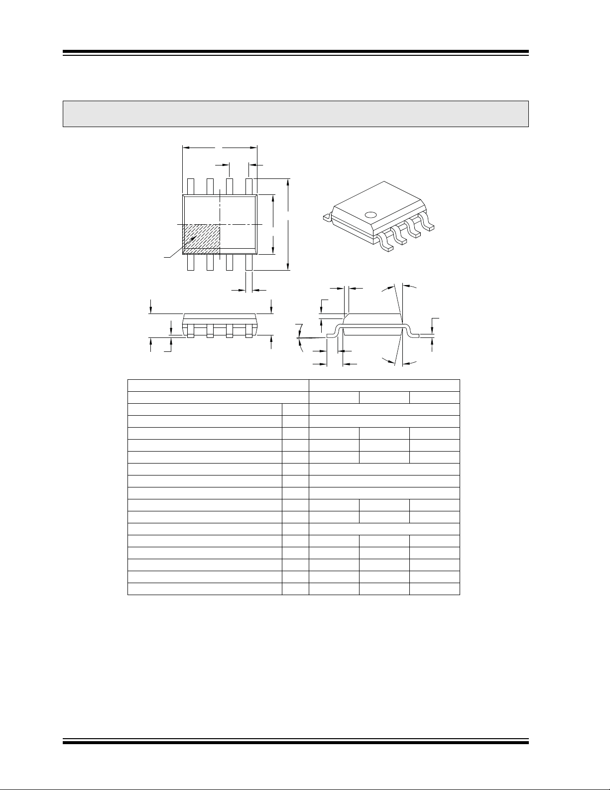
MCP6V06/7/8
/HDG3ODVWLF6PDOO2XWOLQH61±1DUURZPP%RG\>62,&@
1RWHV
3LQYLVXDOLQGH[IHDWXUHPD\YDU\EXWPXVWEHORFDWHGZLWKLQWKHKDWFKHGDUHD
6LJQLILFDQW&KDUDFWHULVWLF
'LPHQVLRQV'DQG(GRQRWLQFOXGHPROGIODVKRUSURWUXVLRQV0ROGIODVKRUSURWUXVLRQVVKDOOQRWH[FHHGPPSHUVLGH
'LPHQVLRQLQJDQGWROHUDQFLQJSHU$60(<0
%6& %DVLF'LPHQVLRQ7KHRUHWLFDOO\H[DFWYDOXHVKRZQZLWKRXWWROHUDQFHV
5() 5HIHUHQFH'LPHQVLRQXVXDOO\ZLWKRXWWROHUDQFHIRULQIRUPDWLRQSXUSRVHVRQO\
1RWH )RUWKHPRVWFXUUHQWSDFNDJHGUDZLQJVSOHDVHVHHWKH0LFURFKLS3DFNDJLQJ6SHFLILFDWLRQORFDWHGDW
KWWSZZZPLFURFKLSFRPSDFNDJLQJ
8QLWV 0,//,0(7(56
'LPHQVLRQ/LPLWV 0,1 120 0$;
1XPEHURI3LQV 1
3LWFK H %6&
2YHUDOO+HLJKW $ ± ±
0ROGHG3DFNDJH7KLFNQHVV $ ± ±
6WDQGRII
$ ±
2YHUDOO:LGWK ( %6&
0ROGHG3DFNDJH:LGWK ( %6&
2YHUDOO/HQJWK ' %6&
&KDPIHURSWLRQDO K ±
)RRW/HQJWK / ±
)RRWSULQW / 5()
)RRW$QJOH ±
/HDG7KLFNQHVV F ±
/HDG:LGWK E ±
0ROG'UDIW$QJOH7RS ±
0ROG'UDIW$QJOH%RWWRP ±
D
N
e
E
E1
NOTE 1
12 3
b
A
A1
A2
L
L1
c
h
h
φ
β
α
0LFURFKLS 7HFKQRORJ\ 'UDZLQJ &%
DS22093A-page 32 © 2008 Microchip Technology Inc.
Page 33
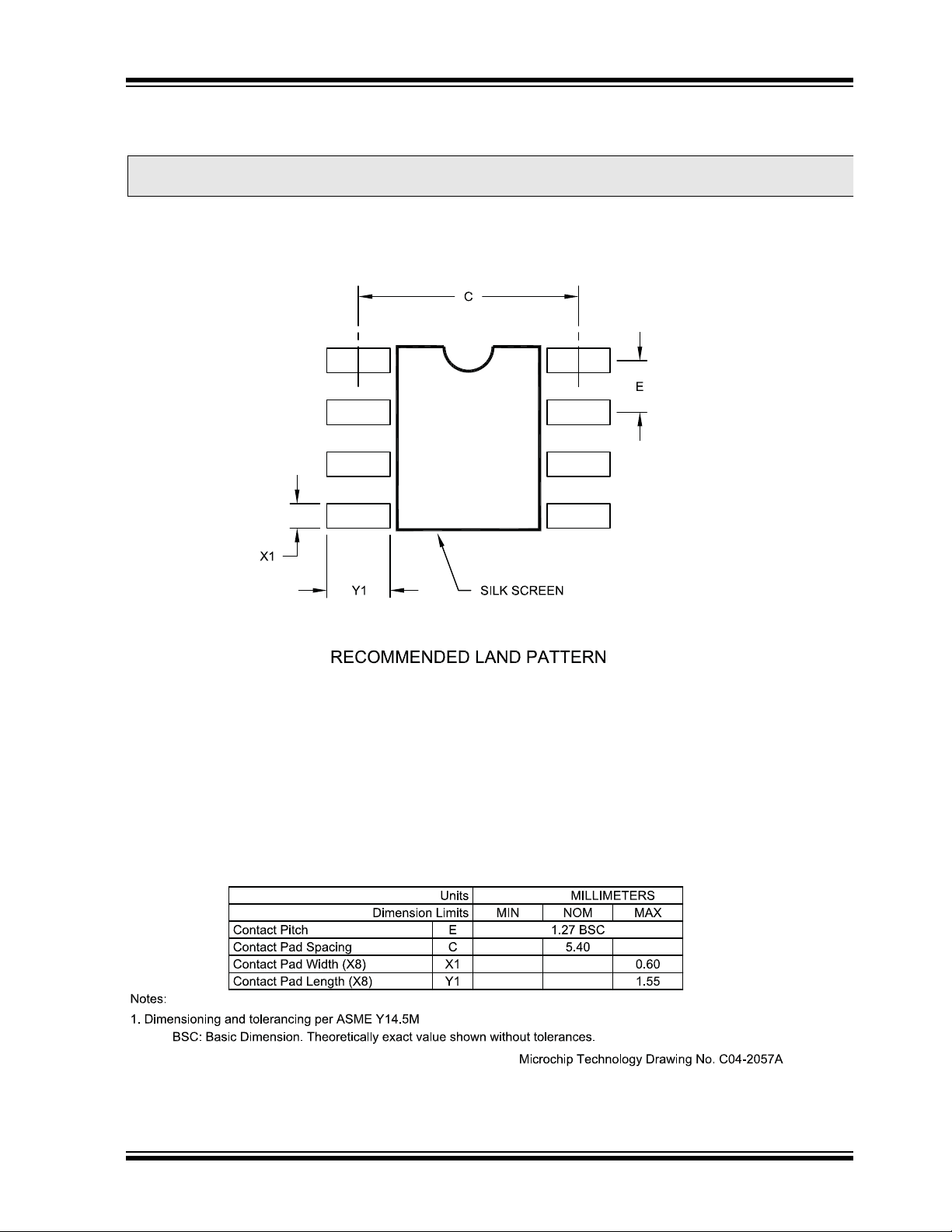
MCP6V06/7/8
/HDG3ODVWLF6PDOO2XWOLQH61±1DUURZPP%RG\>62,&@
1RWH )RUWKHPRVWFXUUHQWSDFNDJHGUDZLQJVSOHDVHVHHWKH0LFURFKLS3DFNDJLQJ6SHFLILFDWLRQORFDWHGDW
KWWSZZZPLFURFKLSFRPSDFNDJLQJ
© 2008 Microchip Technology Inc. DS22093A-page 33
Page 34

MCP6V06/7/8
NOTES:
DS22093A-page 34 © 2008 Microchip Technology Inc.
Page 35

APPENDIX A: REVISION HISTORY
Revision A (June 2008)
• Original Release of this Document.
MCP6V06/7/8
© 2008 Microchip Technology Inc. DS22093A-page 35
Page 36
MCP6V06/7/8
APPENDIX B: OFFSET RELATED
TEST SCREENS
We use production screens to ensure the quality of our
outgoing products. These screens are set at wider lim-
its to eliminate any fliers; see Ta bl e B - 1 .
Input offset voltage related specifications in the DC
spec table (Table 1-1) are based on bench measure-
ments (see Section 2.1 “DC Input Precision”). These
measurements are much more accurate because:
• More compact circuit
• Soldered parts on the PCB
• More time spent averaging (reduces noise)
• Better temperature control
- Reduced temperature gradients
- Greater accuracy
TABLE B-1: OFFSET RELATED TEST SCREENS
Electrical Characteristics: Unless otherwise indicated, TA = 25°C, VDD = +1.8V to +5.5V, VSS = GND, VCM = VDD/3,
V
OUT=VDD
Input Offset
Input Offset Voltage V
Input Offset Voltage Drift with Temperature
(linear Temp. Co.)
Power Supply Rejection PSRR 115 — dB (Note 1)
Common Mode
Common Mode Rejection CMRR 106 — dB V
Open-Loop Gain
DC Open-Loop Gain (large signal) A
Note 1: Due to thermal junctions and other errors in the production environment, these specifications are only screened in
/2, VL=VDD/2, RL = 20 kΩ to VL, and CS = GND (refer to Figure 1-5 and Figure 1-6).
Parameters Sym Min Max Units Conditions
-10 +10 µV TA = +25°C (Note 1, Note 2)
OS
——nV/°CTA = -40 to +125°C (Note 3)
1
= 1.8V, VCM = -0.2V to 2.0V (Note 1)
DD
= 5.5V, VCM = -0.2V to 5.7V (Note 1)
DD
114 — d B VDD= 1.8V, V
OL
122 — dB VDD= 5.5V, V
OL
OUT
OUT
production.
2: V
3: TC
CMRR 116 — dB V
is also sample screened at +125°C.
OS
is not measured in production.
1
TC
A
= 0.2V to 1.6V (Note 1)
= 0.2V to 5.3V (Note 1)
DS22093A-page 36 © 2008 Microchip Technology Inc.
Page 37

MCP6V06/7/8
Device: MCP6V06 Single Op Amp
MCP6V06T Single Op Amp
(Tape and Reel for SOIC)
MCP6V07 Dual Op Amp
MCP6V07T Dual Op Amp
(Tape and Reel for 4×4 DFN and SOIC)
MCP6V08 Single Op Amp with Chip Select
MCP6V08T Single Op Amp with Chip Select
(Tape and Reel for SOIC)
Temperature Range: E = -40°C to +125°C
Package: MD = Plastic Dual Flat, No-Lead (4×4x0.9), 8-lead
(MCP6V07 only)
SN = Plastic SOIC (150mil Body), 8-lead
PART NO. –X /XX
PackageTemperature
Range
Device
Examples:
a) MCP6V06T-E/SN:Extended temperature,
8LD SOIC package.
a) MCP6V07-E/MD: Extended temperature,
8LD 4x4 DFN.
b) MCP6V07T-E/SN:Tape and Reel,
Extended temperature,
8LD SOIC.
a) MCP6V08-E/SN: Extended temperature,
8LD SOIC.
PRODUCT IDENTIFICATION SYSTEM
To order or obtain information, e.g., on pricing or delivery, refer to the factory or the listed sales office.
© 2008 Microchip Technology Inc. DS22093A-page 37
Page 38

MCP6V06/7/8
NOTES:
DS22093A-page 38 © 2008 Microchip Technology Inc.
Page 39

Note the following details of the code protection feature on Microchip devices:
• Microchip products meet the specification contained in their particular Microchip Data Sheet.
• Microchip believes that its family of products is one of the most secure families of its kind on the market today, when used in the
intended manner and under normal conditions.
• There are dishonest and possibly illegal methods used to breach the code protection feature. All of these methods, to our
knowledge, require using the Microchip products in a manner outside the operating specifications contained in Microchip’s Data
Sheets. Most likely, the person doing so is engaged in theft of intellectual property.
• Microchip is willing to work with the customer who is concerned about the integrity of their code.
• Neither Microchip nor any other semiconductor manufacturer can guarantee the security of their code. Code protection does not
mean that we are guaranteeing the product as “unbreakable.”
Code protection is constantly evolving. We at Microchip are committed to continuously improving the code protection features of our
products. Attempts to break Microchip’s code protection feature may be a violation of the Digital Millennium Copyright Act. If such acts
allow unauthorized access to your software or other copyrighted work, you may have a right to sue for relief under that Act.
Information contained in this publication regarding device
applications and the like is provided only for your convenience
and may be superseded by updates. It is your responsibility to
ensure that your application meets with your specifications.
MICROCHIP MAKES NO REPRESENTATIONS OR
WARRANTIES OF ANY KIND WHETHER EXPRESS OR
IMPLIED, WRITTEN OR ORAL, STATUTORY OR
OTHERWISE, RELATED TO THE INFORMATION,
INCLUDING BUT NOT LIMITED TO ITS CONDITION,
QUALITY, PERFORMANCE, MERCHANTABILITY OR
FITNESS FOR PURPOSE. Microchip disclaims all liability
arising from this information and its use. Use of Microchip
devices in life support and/or safety applications is entirely at
the buyer’s risk, and the buyer agrees to defend, indemnify and
hold harmless Microchip from any and all damages, claims,
suits, or expenses resulting from such use. No licenses are
conveyed, implicitly or otherwise, under any Microchip
intellectual property rights.
Trademarks
The Microchip name and logo, the Microchip logo, Accuron,
dsPIC, K
EELOQ, KEELOQ logo, MPLAB, PIC, PICmicro,
PICSTART, PRO MATE, rfPIC and SmartShunt are
registered trademarks of Microchip Technology Incorporated
in the U.S.A. and other countries.
FilterLab, Linear Active Thermistor, MXDEV, MXLAB,
SEEVAL, SmartSensor and The Embedded Control Solutions
Company are registered trademarks of Microchip Technology
Incorporated in the U.S.A.
Analog-for-the-Digital Age, Application Maestro, CodeGuard,
dsPICDEM, dsPICDEM.net, dsPICworks, dsSPEAK, ECAN,
ECONOMONITOR, FanSense, In-Circuit Serial
Programming, ICSP, ICEPIC, Mindi, MiWi, MPASM, MPLAB
Certified logo, MPLIB, MPLINK, mTouch, PICkit, PICDEM,
PICDEM.net, PICtail, PIC
32
logo, PowerCal, PowerInfo,
PowerMate, PowerTool, REAL ICE, rfLAB, Select Mode, Total
Endurance, UNI/O, WiperLock and ZENA are trademarks of
Microchip Technology Incorporated in the U.S.A. and other
countries.
SQTP is a service mark of Microchip Technology Incorporated
in the U.S.A.
All other trademarks mentioned herein are property of their
respective companies.
© 2008, Microchip Technology Incorporated, Printed in the
U.S.A., All Rights Reserved.
Printed on recycled paper.
Microchip received ISO/TS-16949:2002 certification for its worldwide
headquarters, design and wafer fabrication facilities in Chandler and
Tempe, Arizona; Gresham, Oregon and design centers in California
and India. The Company’s quality system processes and procedures
are for its PIC
devices, Serial EEPROMs, microperipherals, nonvolatile memory and
analog products. In addition, Microchip’s quality system for the design
and manufacture of development systems is ISO 9001:2000 certified.
®
MCUs and dsPIC® DSCs, KEELOQ
®
code hopping
© 2008 Microchip Technology Inc. DS22093A-page 39
Page 40

WORLDWIDE SALES AND SERVICE
AMERICAS
Corporate Office
2355 West Chandler Blvd.
Chandler, AZ 85224-6199
Tel: 480-792-7200
Fax: 480-792-7277
Technical Support:
http://support.microchip.com
Web Address:
www.microchip.com
Atlanta
Duluth, GA
Tel: 678-957-9614
Fax: 678-957-1455
Boston
Westborough, MA
Tel: 774-760-0087
Fax: 774-760-0088
Chicago
Itasca, IL
Tel: 630-285-0071
Fax: 630-285-0075
Dallas
Addison, TX
Tel: 972-818-7423
Fax: 972-818-2924
Detroit
Farmington Hills, MI
Tel: 248-538-2250
Fax: 248-538-2260
Kokomo
Kokomo, IN
Tel: 765-864-8360
Fax: 765-864-8387
Los Angeles
Mission Viejo, CA
Tel: 949-462-9523
Fax: 949-462-9608
Santa Clara
Santa Clara, CA
Tel: 408-961-6444
Fax: 408-961-6445
Toronto
Mississauga, Ontario,
Canada
Tel: 905-673-0699
Fax: 905-673-6509
ASIA/PACIFIC
Asia Pacific Office
Suites 3707-14, 37th Floor
Tower 6, The Gateway
Harbour City, Kowloon
Hong Kong
Tel: 852-2401-1200
Fax: 852-2401-3431
Australia - Sydney
Tel: 61-2-9868-6733
Fax: 61-2-9868-6755
China - Beijing
Tel: 86-10-8528-2100
Fax: 86-10-8528-2104
China - Chengdu
Tel: 86-28-8665-5511
Fax: 86-28-8665-7889
China - Hong Kong SAR
Tel: 852-2401-1200
Fax: 852-2401-3431
China - Nanjing
Tel: 86-25-8473-2460
Fax: 86-25-8473-2470
China - Qingdao
Tel: 86-532-8502-7355
Fax: 86-532-8502-7205
China - Shanghai
Tel: 86-21-5407-5533
Fax: 86-21-5407-5066
China - Shenyang
Tel: 86-24-2334-2829
Fax: 86-24-2334-2393
China - Shenzhen
Tel: 86-755-8203-2660
Fax: 86-755-8203-1760
China - Wuhan
Tel: 86-27-5980-5300
Fax: 86-27-5980-5118
China - Xiamen
Tel: 86-592-2388138
Fax: 86-592-2388130
China - Xian
Tel: 86-29-8833-7252
Fax: 86-29-8833-7256
China - Zhuhai
Tel: 86-756-3210040
Fax: 86-756-3210049
ASIA/PACIFIC
India - Bangalore
Tel: 91-80-4182-8400
Fax: 91-80-4182-8422
India - New Delhi
Tel: 91-11-4160-8631
Fax: 91-11-4160-8632
India - Pune
Tel: 91-20-2566-1512
Fax: 91-20-2566-1513
Japan - Yokohama
Tel: 81-45-471- 6166
Fax: 81-45-471-6122
Korea - Daegu
Tel: 82-53-744-4301
Fax: 82-53-744-4302
Korea - Seoul
Tel: 82-2-554-7200
Fax: 82-2-558-5932 or
82-2-558-5934
Malaysia - Kuala Lumpur
Tel: 60-3-6201-9857
Fax: 60-3-6201-9859
Malaysia - Penang
Tel: 60-4-227-8870
Fax: 60-4-227-4068
Philippines - Manila
Tel: 63-2-634-9065
Fax: 63-2-634-9069
Singapore
Tel: 65-6334-8870
Fax: 65-6334-8850
Taiwan - Hsin Chu
Tel: 886-3-572-9526
Fax: 886-3-572-6459
Taiwan - Kaohsiung
Tel: 886-7-536-4818
Fax: 886-7-536-4803
Taiwan - Taipei
Tel: 886-2-2500-6610
Fax: 886-2-2508-0102
Thailand - Bangkok
Tel: 66-2-694-1351
Fax: 66-2-694-1350
EUROPE
Austria - Wels
Tel: 43-7242-2244-39
Fax: 43-7242-2244-393
Denmark - Copenhagen
Tel: 45-4450-2828
Fax: 45-4485-2829
France - Paris
Tel: 33-1-69-53-63-20
Fax: 33-1-69-30-90-79
Germany - Munich
Tel: 49-89-627-144-0
Fax: 49-89-627-144-44
Italy - Milan
Tel: 39-0331-742611
Fax: 39-0331-466781
Netherlands - Drunen
Tel: 31-416-690399
Fax: 31-416-690340
Spain - Madrid
Tel: 34-91-708-08-90
Fax: 34-91-708-08-91
UK - Wokingham
Tel: 44-118-921-5869
Fax: 44-118-921-5820
01/02/08
DS22093A-page 40 © 2008 Microchip Technology Inc.
 Loading...