

M
Single-Ended, Rail-to-Rail I/O, Low Gain PGA
MCP6S21/2/6/8
Features
• Multiplexed Inputs: 1, 2, 6 or 8 channels
• 8 Gain Selections:
- +1, +2, +4, +5, +8, +10, +16 or +32 V/V
• Serial Peripheral Interface (SPI™)
• Rail-to-Rail Input and Output
• Low Gain Error: ±1% (max)
• Low Offset: ±275 µV (max)
• High Bandwidth: 2 to 12 MHz (typ)
• Low Noise: 10 nV/√Hz @ 10 kHz (typ)
• Low Supply Current: 1.0 mA (typ)
• Single Supply: 2.5V to 5.5V
Typical Applications
• A/D Converter Driver
• Multiplexed Analog Applications
• Data Acquisition
• Industrial Instrumentation
• Test Equipment
• Medical Instrumentation
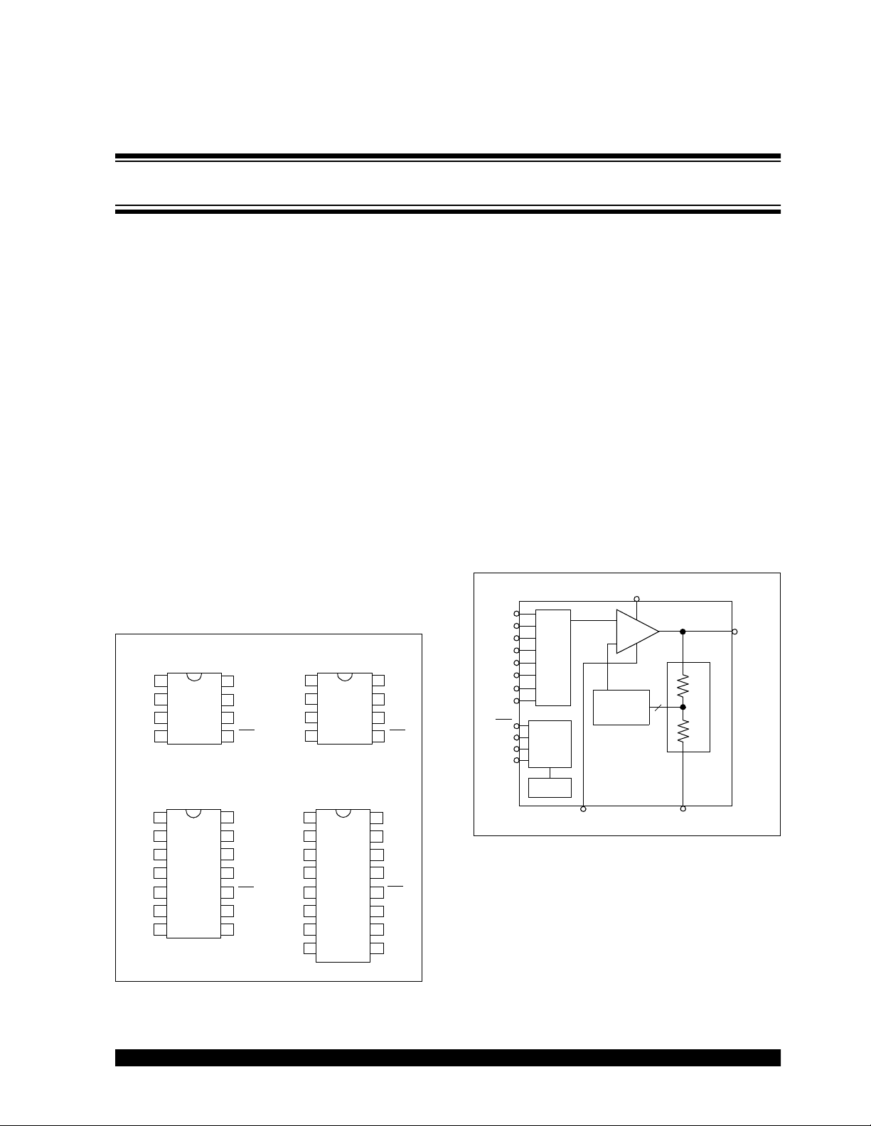
Package Types
MCP6S21
PDIP, SOIC, MSOP
V
1
OUT
CH0
2
V
3
REF
V
4
SS
V
8
DD
SCK
7
SI
6
5
CS
MCP6S22
PDIP, SOIC, MSOP
V
1
OUT
CH0
2
3
CH1
V
4
SS
Description
The Microchip Technology Inc. MCP6S21/2/6/8 are
analog Programmable Gain Amplifiers (PGA). They
can be configured for gains from +1 V/V to +32 V/V and
the input multiplexer can select one of up to eight channels through an SPI port. The serial interface can also
put the PGA into shutdown to conserve power. These
PGAs are optimized for high speed, low offset voltage
and single-supply operation with rail-to-rail input and
output capability. These specifications support single
supply applications needing flexible performance or
multiple inputs.
The one channel MCP6S21 and the two channel
MCP6S22 are available in 8-pin PDIP, SOIC and
MSOP packages. The six channel MCP6S26 is available in 14-pin PDIP, SOIC and TSSOP packages. The
eight channel MCP6S28 is available in 16-pin PDIP
and SOIC packages. All parts are fully specified from
-40°C to +85°C.
Block Diagram
V
DD
CH0
CH1
CH2
CH3
CH4
V
8
DD
SCK
7
SI
6
5
CS
CH5
CH6
CH7
CS
SO
SCK
MUX
SI
SPI™
Logic
+
-
Gain
Switches
V
OUT
Resistor Ladder (R
R
8
F
R
G
LAD
)
MCP6S26
PDIP, SOIC, TSSOP
V
1
OUT
CH0
2
CH1
3
CH2
4
5
CH3
CH4
6
7
CH5
2003 Microchip Technology Inc. DS21117A-page 1
14
13
12
11
10
V
DD
SCK
SO
SI
CS
V
9
SS
V
8
REF
V
OUT
CH0
CH1
CH2
CH3
CH4
CH5
CH6
MCP6S28
PDIP, SOIC
1
2
3
4
5
6
7
8
16
15
14
13 SI
12
11
10
9
V
DD
SCK
SO
CS
V
SS
V
REF
CH7
POR
V
SS
V
REF
MCP6S21/2/6/8
1.0 ELECTRICAL CHARACTERISTICS
Absolute Maximum Ratings †
VDD - VSS.........................................................................7.0V
All inputs and outputs....................... V
Difference Input voltage ........................................ |V
Output Short Circuit Current...................................continuous
Current at Input Pin .............................................................±2mA
Current at Output and Supply Pins ................................ ±30 mA
Storage temperature .....................................-65°C to +150°C
Junction temperature .................................................. +150°C
ESD protection on all pins (HBM;MM).................. ≥ 2 kV; 200V
- 0.3V to VDD +0.3V
SS
DD
- VSS|
PIN FUNCTION TABLE
Name Function
V
OUT
CH0-CH7 Analog Inputs
V
SS
V
DD
SCK SPI Clock Input
SI SPI Serial Data Input
SO SPI Serial Data Output
CS
V
REF
Analog Output
Negative Power Supply
Positive Power Supply
SPI Chip Select
External Reference Pin
† Notice: Stresses above those listed under "Maximum
Ratings" may cause permanent damage to the device. This is
a stress rating only and functional operation of the device at
those or any other conditions above those indicated in the
operation listings of this specification is not implied. Exposure
to maximum rating conditions for extended periods may affect
device reliability.
DC CHARACTERISTICS
Electrical Specifications: Unless otherwise indicated, TA=+25°C, VDD= +2.5V to +5.5V, VSS= GND, V
Input = CH0 = (0.3V)/G, CH1 to CH7 = 0.3V, R
=10kΩ to VDD/2, SI and SCK are tied low and CS is tied high.
L
Parameters Sym Min Typ Max Units Conditions
Amplifier Input
Input Offset Voltage V
Input Offset Voltage Drift ∆V
OS
OS
/∆T
-275 — +275 µV G = +1, VDD = 4.0V
—±4 —µV/°CT
A
= -40 to +85°C
A
Power Supply Rejection Ratio PSRR 70 85 — dB G = +1 (Note 1)
Input Bias Current I
Input Bias Current over
Temperature
Input Impedance Z
Input Voltage Range V
B
I
B
IN
IVR
— ±1 — pA CHx = VDD/2
— — 250 pA TA = -40 to +85°C,
CHx = V
—1013||15 — Ω||pF
VSS−0.3 — VDD+0.3 V
Amplifier Gain
Nominal Gains G — 1 to 32 — V/V +1, +2, +4, +5, +8, +10, +16 or +32
DC Gain Error G = +1 g
G ≥ +2 g
E
E
DC Gain Drift G = +1 ∆G/∆T
G ≥ +2 ∆G/∆T
Internal Resistance R
Internal Resistance over
∆R
LAD
LAD
Temperature
-0.1 — +0.1 % V
-1.0 — +1.0 % V
— ±0.0002 — %/°C TA = -40 to +85°C
A
— ±0.0004 — %/°C TA = -40 to +85°C
A
3.4 4.9 6.4 kΩ (Note 1)
/∆T
—+0.028 — %/°C(Note 1)
A
≈ 0.3V to V
OUT
≈ 0.3V to V
OUT
T
= -40 to +85°C
A
Amplifier Output
DC Output Non-linearity G = +1 V
G ≥ +2 V
Maximum Output Voltage Swing V
Short-Circuit Current I
Note 1: R
(RF + RG in Figure 4-1) connects V
LAD
V
tied internally to VSS, so VSS is coupled to the internal amplifier and the PSRR spec describes PSRR+ only. We
REF
recommend the MCP6S22’s V
2: I
includes current in R
Q
3: The output goes Hi-Z and the registers reset to their defaults; see Section 5.4, “Power-On Reset”.
ONL
ONL
, VOLVSS+20 — VDD-100 mV G ≥ +2; 0.5V output overdrive
OH
O(SC)
SS
(typically 60 µA at V
LAD
— ±0.003 — % of FSR V
— ±0.001 — % of FSR V
+60 — VDD-60 G ≥ +2; 0.5V output overdrive,
V
SS
—±30 — mA
, V
REF
and the inverting input of the internal amplifier. The MCP6S22 has
OUT
pin be tied directly to ground to avoid noise problems.
= 0.3V). Both IQ and I
OUT
Q_SHDN
= 0.3V to V
OUT
= 0.3V to V
OUT
V
= VDD/2
REF
exclude digital switching currents.
= VSS, G = +1 V/V,
REF
/2
DD
DD
DD
DD
DD
− 0.3V
− 0.3V
− 0.3V, V
− 0.3V, V
DD
DD
= 5.0V
= 5.0V
DS21117A-page 2 2003 Microchip Technology Inc.
DC CHARACTERISTICS (CONTINUED)
MCP6S21/2/6/8
Electrical Specifications: Unless otherwise indicated, TA=+25°C, VDD= +2.5V to +5.5V, VSS= GND, V
Input = CH0 = (0.3V)/G, CH1 to CH7 = 0.3V, R
=10kΩ to VDD/2, SI and SCK are tied low and CS is tied high.
L
Parameters Sym Min Typ Max Units Conditions
Power Supply
Supply Voltage V
Quiescent Current I
Quiescent Current, Shutdown
I
Q_SHDN
DD
Q
2.5 — 5.5 V
0.5 1.0 1.35 mA IO = 0 (Note 2)
—0.51.0 µAI
= 0 (Note 2)
O
mode
Power-On Reset
POR Trip Voltage V
POR Trip Voltage Drift ∆V
Note 1: R
2: I
3: The output goes Hi-Z and the registers reset to their defaults; see Section 5.4, “Power-On Reset”.
(RF + RG in Figure 4-1) connects V
LAD
V
tied internally to VSS, so VSS is coupled to the internal amplifier and the PSRR spec describes PSRR+ only. We
REF
recommend the MCP6S22’s V
includes current in R
Q
POR
POR
(typically 60 µA at V
LAD
1.2 1.7 2.2 V (Note 3)
/∆T— -3.0 — mV/°CTA = -40°C to+85°C
, V
REF
pin be tied directly to ground to avoid noise problems.
SS
and the inverting input of the internal amplifier. The MCP6S22 has
OUT
= 0.3V). Both IQ and I
OUT
exclude digital switching currents.
Q_SHDN
AC CHARACTERISTICS
Electrical Specifications: Unless otherwise indicated, TA=+25°C, VDD= +2.5V to +5.5V, VSS= GND, V
Input = CH0 =(0.3V)/G, CH1 to CH7=0.3V, R
Parameters Sym Min Typ Max Units Conditions
Frequency Response
-3 dB Bandwidth BW — 2 to 12 — MHz All gains; V
Gain Peaking GPK — 0 — dB All gains; V
Total Harmonic Distortion plus Noise
f = 1 kHz, G = +1 V/V THD+N — 0.0015 — %
f = 1 kHz, G = +4 V/V THD+N — 0.0058 — %
f = 1 kHz, G = +16 V/V THD+N — 0.023 — %
f = 20 kHz, G = +1 V/V THD+N — 0.0035 — %
f = 20 kHz, G = +4 V/V THD+N — 0.0093 — %
f = 20 kHz, G = +16 V/V THD+N — 0.036 — %
Step Response
Slew Rate SR — 4.0 — V/µs G = 1, 2
Noise
Input Noise Voltage E
Input Noise Voltage Density e
Input Noise Current Density i
Note 1: See Table 4-1 for a list of typical numbers.
and eni include ladder resistance noise. See Figure 2-33 for eni vs. G data.
2: E
ni
=10kΩ to VDD/2, CL = 60 pF, SI and SCK are tied low, and CS is tied high.
L
= 1.5V ± 1.0VPK, VDD = 5.0V,
V
OUT
BW = 22 kHz
V
= 1.5V ± 1.0VPK, VDD = 5.0V,
OUT
BW = 22 kHz
V
= 1.5V ± 1.0VPK, VDD = 5.0V,
OUT
BW = 22 kHz
V
= 1.5V ± 1.0VPK, VDD = 5.0V,
OUT
BW = 80 kHz
V
= 1.5V ± 1.0VPK, VDD = 5.0V,
OUT
BW = 80 kHz
V
= 1.5V ± 1.0VPK, VDD = 5.0V,
OUT
BW = 80 kHz
— 11 — V/µs G = 4, 5, 8, 10
—22—V/µsG = 16, 32
ni
—3.2—µV
f = 0.1 Hz to 10 kHz (Note 2)
P-P
— 26 — f = 0.1 Hz to 200 kHz (Note 2)
ni
ni
—10—nV/√Hz f = 10 kHz (Note 2)
—4—fA/√Hz f = 10 kHz
= VSS, G = +1 V/V,
REF
= VSS, G = +1 V/V,
REF
< 100 mV
OUT
< 100 mV
OUT
(Note 1)
P-P
P-P
2003 Microchip Technology Inc. DS21117A-page 3
MCP6S21/2/6/8
DIGITAL CHARACTERISTICS
Electrical Specifications: Unless otherwise indicated, TA=+25°C, VDD= +2.5V to +5.5V, VSS= GND, V
Input = CH0 = (0.3V)/G, CH1 to CH7 = 0.3V, R
Parameters Sym Min Typ Max Units Conditions
=10kΩ to VDD/2, CL = 60 pF, SI and SCK are tied low, and CS is tied high.
L
= VSS, G = +1 V/V,
REF
SPI Inputs (CS
Logic Threshold, Low V
Input Leakage Current I
Logic Threshold, High V
, SI, SCK)
IL
IL
IH
0 — 0.3V
-1.0 — +1.0 µA
0.7V
—VDDV
DD
DD
V
Amplifier Output Leakage Current — -1.0 — +1.0 µA In Shutdown mode
SPI Output (SO, for MCP6S26 and MCP6S28)
Logic Threshold, Low V
Logic Threshold, High V
OL
OH
V
SS
VDD-0.5 — V
—VSS+0.4 V IOL = 2.1 mA, VDD = 5V
DD
VIOH = -400 µA
SPI Timing
Pin Capacitance C
Input Rise/Fall Times (CS
, SI, SCK)
Output Rise/Fall Times (SO) t
high time
CS
SCK edge to CS
CS
fall to first SCK edge setup time
fall setup time
SCK Frequency f
SCK high time t
SCK low time t
SCK last edge to CS
CS
rise to SCK edge setup time
rise setup time
SI set-up time t
SI hold time t
SCK to SO valid propagation delay t
rise to SO forced to zero
CS
PIN
t
RFI
RFO
t
CSH
t
CS0
t
CSSC
SCK
LO
t
SCCS
t
CS1
SU
HD
DO
t
SOZ
HI
— 10 — pF All digital I/O pins
——2µsNote 1
— 5 — ns MCP6S26 and MCP 6S28
40 — — ns
10 — — ns
SCK edge when CS is high
40 — — ns
——10MHzVDD = 5V (Note 2)
40 — — ns
40 — — ns
30 — — ns
100 — — ns
SCK edge when CS is high
40 — — ns
10 — — ns
— — 80 ns MCP6S26 and MCP 6S28
— — 80 ns MCP6S26 and MCP 6S28
Channel and Gain Select Timing
Channel Select Time t
Gain Select Time t
CH
G
— 1.5 — µs CHx = 0.6V, CHy =0.3V, G = 1,
CHx to CHy select
C
S = 0.7VDD to V
OUT
— 1 — µs CHx = 0.3V, G = 5 to G = 1 select,
C
S = 0.7VDD to V
OUT
Shutdown Mode Timing
Out of Shutdown mode (CS
goes
high) to Amplifier Output Turn-on
t
ON
—3.510µs
CS
= 0.7VDD to V
OUT
90% point
Time
Into Shutdown mode (CS
goes high)
to Amplifier Output High-Z Turn-off
t
OFF
—1.5—µs
CS
= 0.7VDD to V
OUT
90% point
Time
POR Timing
Power-On Reset power-up time t
Power-On Reset power-down time t
RPU
RPD
—30—µsVDD = V
50% V
—10—µsVDD = V
50% V
POR
to 90% V
DD
POR
to 90% V
DD
- 0.1V to V
OUT
+ 0.1V to V
OUT
Note 1: Not tested in production. Set by design and characterization.
2: When using the device in the daisy chain configuration, maximum clock frequency is determined by a combination of
propagation delay time (t
fall times of 5 ns. Maximum f
≤ 80 ns), data input setup time (tSU ≥ 40 ns), SCK high time (tHI ≥ 40 ns), and SCK rise and
DO
is, therefore, ≈ 5.8 MHz.
SCK
90% point
90% point
+ 0.1V,
POR
point
- 0.1V,
POR
point
DS21117A-page 4 2003 Microchip Technology Inc.

TEMPERATURE CHARACTERISTICS
MCP6S21/2/6/8
Electrical Specifications: Unless otherwise indicated, V
= +2.5V to +5.5V, VSS= GND.
DD
Parameters Sym Min Typ Max Units Conditions
Temperature Ranges
Specified Temperature Range T
Operating Temperature Range T
Storage Temperature Range T
A
A
A
-40 — +85 °C
-40 — +125 °C (Note Note:)
-65 — +150 °C
Thermal Package Resistances
Thermal Resistance, 8L-PDIP θ
Thermal Resistance, 8L-SOIC θ
Thermal Resistance, 8L-MSOP θ
Thermal Resistance, 14L-PDIP θ
Thermal Resistance, 14L-SOIC θ
Thermal Resistance, 14L-TSSOP θ
Thermal Resistance, 16L-PDIP θ
Thermal Resistance, 16L-SOIC θ
JA
JA
JA
JA
JA
JA
JA
JA
—85—°C/W
—163—°C/W
—206—°C/W
—70—°C/W
—120—°C/W
—100—°C/W
—70—°C/W
—90—°C/W
Note 1: The MCP6S21/2/6/8 family of PGAs operates over this extended temperature range, but with reduced
performance. Operation in this range must not cause T
to exceed the Maximum Junction Temperature
J
(150°C).
CS
CS
t
CH
V
OUT
0.6V
0.3V
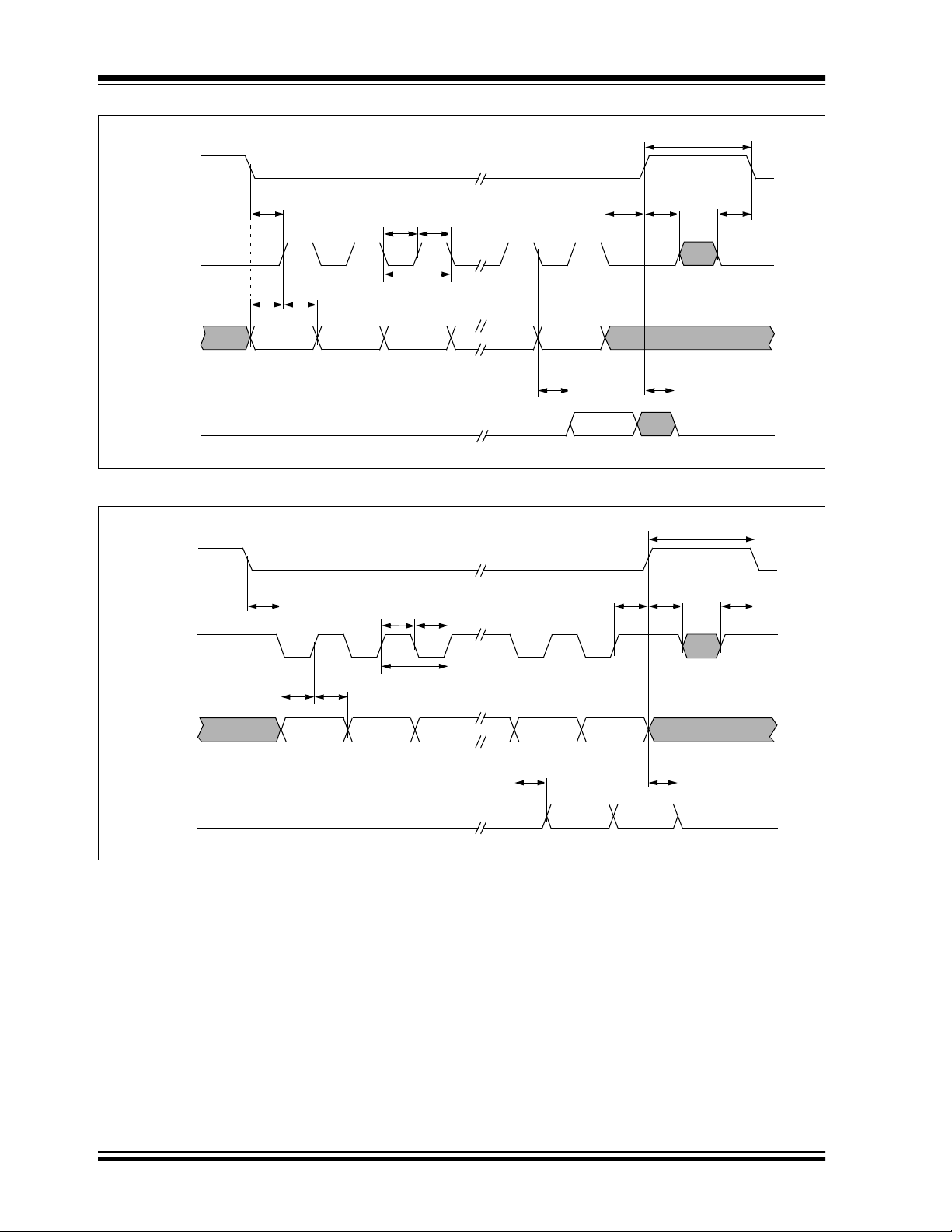
FIGURE 1-1: Channel Select Timing Diagram.
CS
t
OFF
V
OUT
I
SS
t
ON
Hi-Z Hi-Z
0.3V
1.0 mA (typ)
500 nA (typ)
FIGURE 1-2: PGA Shutdown timing
diagram (must enter correct commands before
CS
goes high).
t
G
V
OUT
1.5V
0.3V
FIGURE 1-3: Gain Select Timing Diagram.
V
+ 0.1V
t
RPU
POR
0.3V
1.0 mA (typ)
t
RPD
POR
- 0.1V
V
V
OUT
DD
V
- 0.1V V
POR
Hi-Z Hi-Z
I
SS
500 nA (typ)
FIGURE 1-4: POR power-up and powerdown timing diagram.
2003 Microchip Technology Inc. DS21117A-page 5
MCP6S21/2/6/8
CS
t
CSH
t
CSSC
tLOt
HI
SCK
1/f
t
t
HD
SU
SCK
SI
t
DO
SO
(first 16 bits out are always zeros)
FIGURE 1-5: Detailed SPI Serial Interface Timing, SPI 0,0 mode.
CS
t
CSSC
tHIt
LO
SCK
t
SCCS
t
SCCS
t
CS1
t
SOZ
t
CS1
t
CSH
t
CS0
t
CS0
1/f
tSUt
HD
SCK
SI
t
DO
SO
(first 16 bits out are always zeros)
FIGURE 1-6: Detailed SPI Serial Interface Timing, SPI 1,1 mode.
t
SOZ
DS21117A-page 6 2003 Microchip Technology Inc.
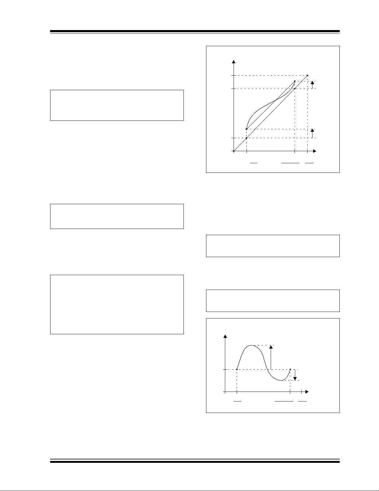
1.1 DC Output Voltage Specs / Model
1.1.1 IDEAL MODEL
MCP6S21/2/6/8
V
(V)
OUT
The ideal PGA output voltage (V
OUT
) is:
EQUATION
V
O_ideal
where: G is the nominal gain
(see Figure 1-7). This equation holds when there are
no gain or offset errors and when the V
a low impedance source (<< 0.1Ω) at ground potential
(V
= 0V).
SS
GV
= V
IN
REFVSS
pin is tied to
REF
0V==
1.1.2 LINEAR MODEL
The PGA’s linear region of operation, including offset
and gain errors, is modeled by the line V
O_linear
, shown
in Figure 1-7.
EQUATION
V
O_linear
V
The endpoints of this line are at V
V
-0.3V. The gain and offset specifications referred to
DD
in the electrical specifications are related to Figure 1-7,
as follows:
G1 g
REFVSS
+()V
E
0V==
IN
0.3 V V
+–()0.3V+=
O_ideal
OS
=0.3V and
EQUATION
V
DD
V
DD
2
V
1
V
(V)
IN
V
-0.3
DD
T
U
O
r
V
O
V
l
a
a
e
e
n
d
i
i
l
_
_
O
V
0.3
0
0.3 V
0
- 0.3 V
DD
GGG
FIGURE 1-7: Output Voltage Model with
the standard condition V
= VSS = 0V.
REF
1.1.3 OUTPUT NON-LINEARITY
Figure 1-8 shows the Integral Non-Linearity (INL) of the
output voltage.
EQUATION
INL V
The output non-linearity specification in the electrical
specifications is related to Figure 1-8 by:
–=
OUTVO_linear
gE100%
V
OS
∆⁄∆
GT
A
---------- ------------- --
=
G1 g
g
∆
----------
=
T
∆
V
2V1
----------- ------------- --------------=
GV
DD
V
1
+()
E
E
A
–
0.6V–()
G+1=
EQUATION
max V4V3,{}
ONL
---------- ------------- ----------
=
V
DD
0.6 V–
V
INL (V)
V
4
0
0.3 V
0
DD
V
3
(V)
V
- 0.3 V
IN
DD
GGG
FIGURE 1-8: Output Voltage INL with the
standard condition V
= VSS = 0V.
REF
2003 Microchip Technology Inc. DS21117A-page 7

MCP6S21/2/6/8
1.1.4 DIFFERENT V
CONDITIONS
REF
Some of the plots in Section 2.0, “Typical Performance
Curves”, have the conditions V
V
REF=VDD
. The equations and figures above are eas-
REF=VDD
ily modified for these conditions. The ideal V
/2 or
OUT
becomes:
EQUATION
V
O_idealVREF
V
DDVREFVSS
The complete linear model is:
GVINV
> 0V=≥
–()+=
REF
EQUATION
V
O_linear
where the new VIN endpoints are:
G1 g
+()V
E
INVIN_LVOS
+–()0.3 V+=
EQUATION
0.3V V
–
GV
+
REF
0.3V– V
GV
+
REF
REF
–
REF
V
V
=
IN_L
V
---------- ------------- ------------- -----------
=
IN_R
---------- ------------- -------
DD
The equations for extracting the specifications do not
change.
DS21117A-page 8 2003 Microchip Technology Inc.
MCP6S21/2/6/8
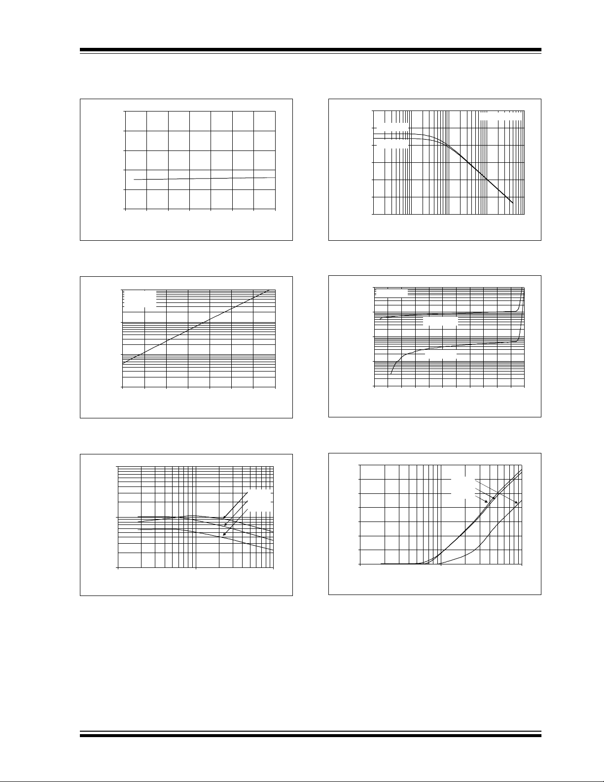
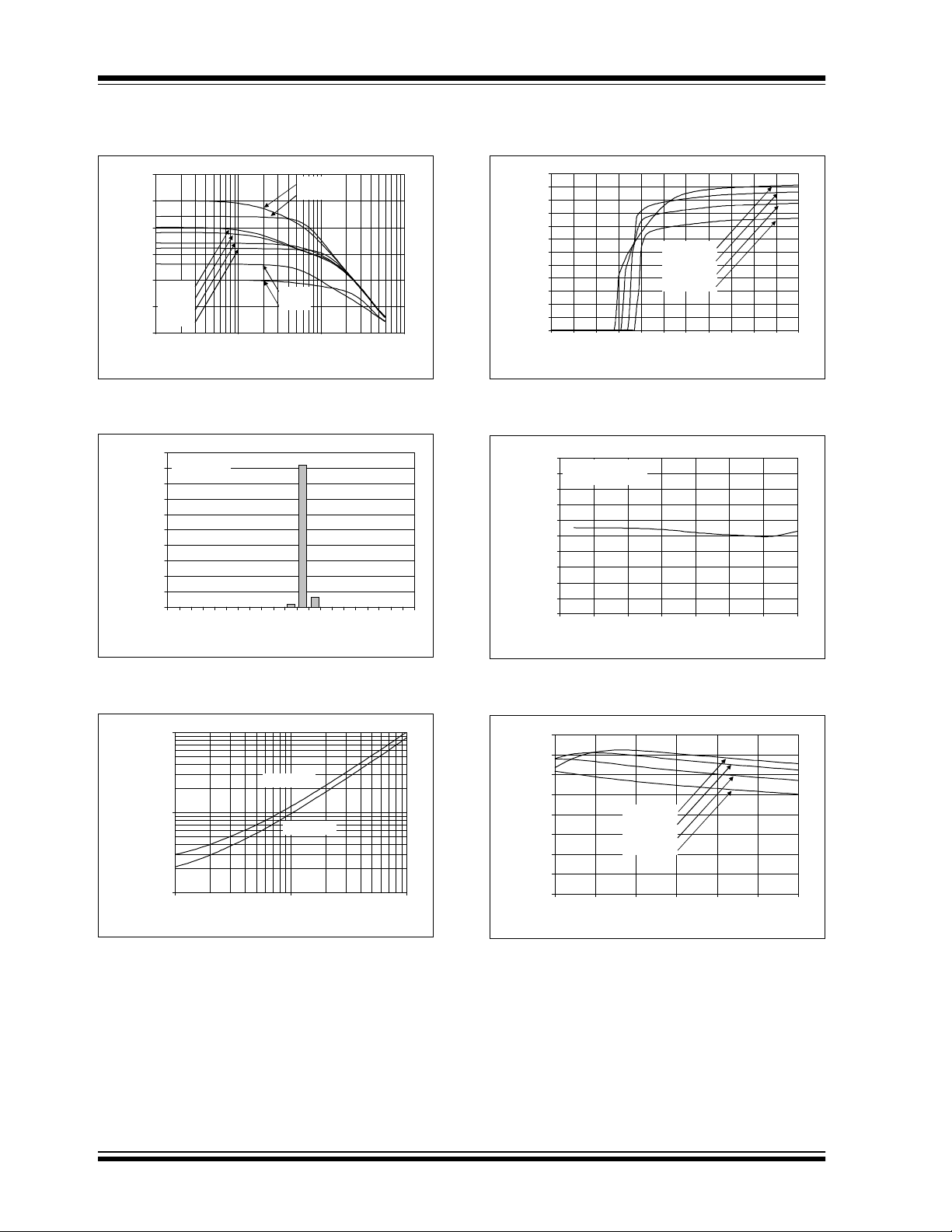
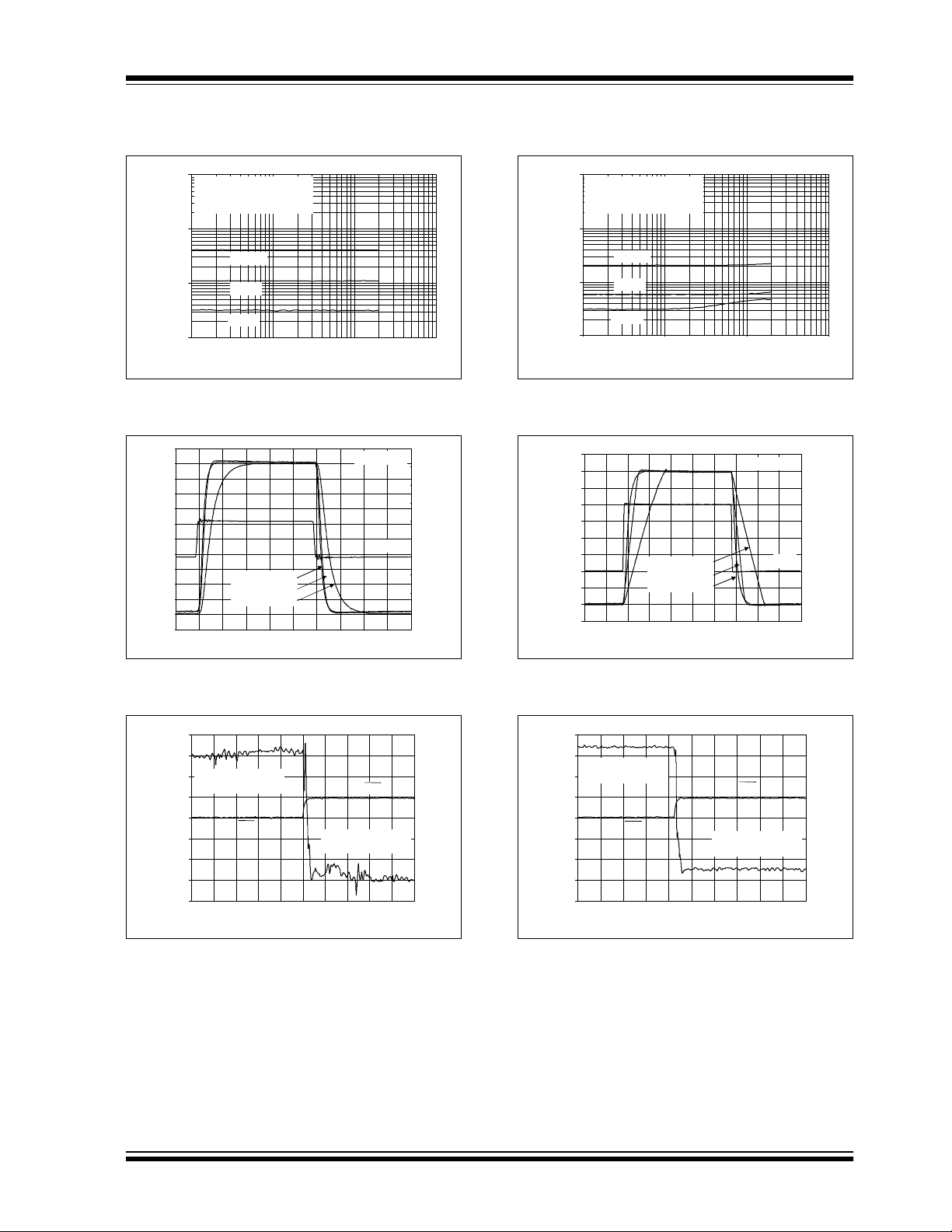
2.0 TYPICAL PERFORMANCE CURVES
Note: The graphs and tables provided following this note are a statistical summary based on a limited number of
samples and are provided for informational purposes only. The performance characteristics listed herein
are not tested or guaranteed. In some graphs or tables, the data presented may be outside the specified
operating range (e.g., outside specified power supply range) and therefore outside the warranted range.
Note: Unless otherwise indicated, T
Input = CH0 = (0.3V)/G, CH1 to CH7 = 0.3V, R
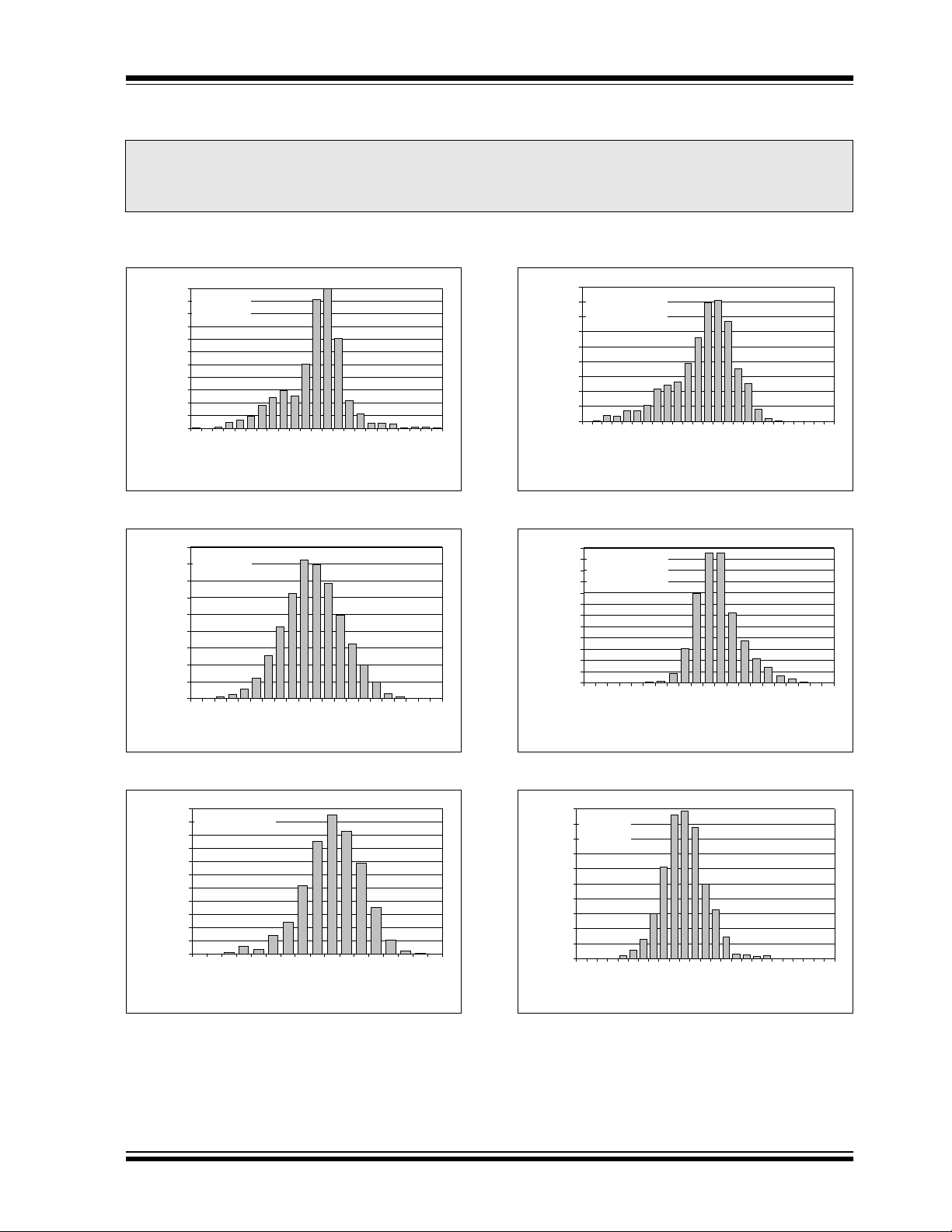
22%
420 Samp les
20%
G = +1
18%
16%
14%
12%
10%
8%
6%
4%
2%
Percentage of Occurrences
0%
-0.040
-0.036
-0.032
-0.028
-0.024
-0.020
= +25°C, V
A
-0.016
-0.012
-0.008
L
-0.004
DC Gain Error (%)
FIGURE 2-1: DC Gain Error, G = +1.
18%
420 Samples
16%
G t +2
14%
12%
10%
8%
6%
4%
2%
Percentage of Occurrences
0%
0.0
0.1
0.2
-0.5
-0.4
-0.3
-0.2
-0.1
DC Gain Error (%)
0.3
= +5.0V, V
DD
= GND, V
SS
REF =VSS
=10kΩ to VDD/2, and CL = 60 pF.
18%
420 Samp les
16%
G = +1
14%
T
= -40 to +125°C
A
12%
10%
8%
6%
4%
2%
0%
Percentage of Occurrences
0.000
0.004
-0.0006
FIGURE 2-4: DC Gain Drift, G = +1.
24%
420 Samples
22%
G t +2
20%
= -40 to +125°C
T
A
18%
16%
14%
12%
10%
8%
6%
4%
2%
Percentage of Occurrences
0%
0.4
0.5
-0.0020
, G= +1 V/V,
-0.0005
-0.0004
-0.0003
DC Gain Drift (%/°C)
-0.0016
-0.0012
DC Gain Drift (%/°C)
-0.0002
-0.0008
-0.0001
-0.0004
0.0000
0.0000
0.0001
0.0004
0.0002
0.0008
0.0003
0.0012
0.0004
0.0005
0.0016
0.0006
0.0020
FIGURE 2-2: DC Gain Error, G ≥+2.
22%
420 Samp les
20%
T
= -40 to +125°C
A
18%
16%
14%
12%
10%
8%
6%
4%
2%
Percentage of Occurrences
0%
0.023
0.024
0.025
0.026
0.027
0.028
0.029
0.030
Ladder Resistance Drift (%/°C)
FIGURE 2-3: Ladder Resistance Drift.
0.031
FIGURE 2-5: DC Gain Drift, G ≥+2.
20%
360 Samples
18%
VDD = 4.0 V
16%
G = +1
14%
12%
10%
8%
6%
4%
2%
Percentage of Occurrences
0%
-240
-200
-160
-120
-80
-40
0
40
80
120
160
Input Offset Voltage (µV)
FIGURE 2-6: Input Offset Voltage,
= 4.0V.
V
DD
200
240
2003 Microchip Technology Inc. DS21117A-page 9
MCP6S21/2/6/8
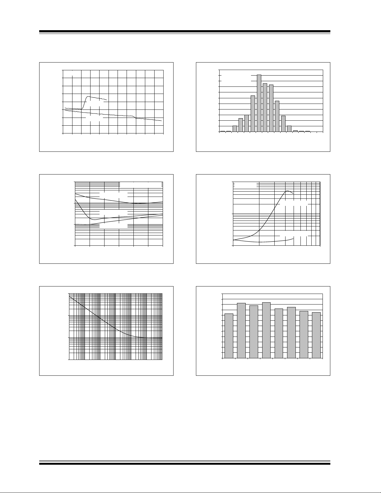
Note: Unless otherwise indicated, T
Input = CH0 = (0.3V)/G, CH1 to CH7 = 0.3V, R
200
G = +1
150
100
50
0
-50
-100
-150
Input Offset Voltage (µV)
-200
0.00.51.01.52.02.53.03.54.04.55.05.5
VDD = +2.5
VDD = +5.5
V
Voltage (V)
REF
= +25°C, V
A
L
FIGURE 2-7: Input Offset Voltage vs.
V
Voltage.
REF
0.01
0.001
0.0001
DC Output Non-Linearity,
Input Referred (% of FSR)
0.00001
2.5 3.0 3.5 4.0 4.5 5.0 5.5
Power Supply Voltage (V)
V
V
V
/G, G = +1
ONL
/G, G = +2
ONL
/G, G t +4
ONL
V
= 0.3V to VDD -0.3V
OUT
= +5.0V, V
DD
= GND, V
SS
REF =VSS
=10kΩ to VDD/2, and CL = 60 pF.
22%
420 Samples
20%
TA = -40 to +125°C
18%
G = +1
16%
14%
12%
10%
8%
6%
4%
2%
Percentage of Occurrences
0%
-16
-14
FIGURE 2-10: Input Offset Voltage Drift.
0.0100%
0.0010%
Input Referred (%)
DC Output Non-Linearity,
0.0001%
VDD = +5.5 V
110
, G= +1 V/V,
-8-6-4
-12
-10
Input Offset Voltage Drift (µV/° C)
Output Voltage Swing (V
02468
-2
V
V
ONL
ONL
/G, G = +1
/G, G t +2
P-P
101214
)
16
FIGURE 2-8: DC Output Non-Linearity vs. Supply Voltage.
1000
100
Hz)
(nV/
10
Input Noise Voltage Density
1
0.1 1 10 100 1000 10000 100000
1k 10k 100k1 10 1000.1
Frequency (Hz)
FIGURE 2-9: Input Noise Voltage Density vs. Frequency.
FIGURE 2-11: DC Output Non-Linearity vs. Output Swing.
12
f = 10 kHz
11
10
9
8
7
Hz)
6
5
(nV/
4
3
2
1
Input Noise Voltage Density
0
12458101632
Gain (V/V)
FIGURE 2-12: Input Noise Voltage Density vs. Gain.
DS21117A-page 10 2003 Microchip Technology Inc.
MCP6S21/2/6/8
Note: Unless otherwise indicated, T
=+25°C, V
A
Input = CH0 = (0.3V)/G, CH1 to CH7 = 0.3V, R
120
110
100
(dB)
90
80
Power Supply Rejection Ratio
70
-50 -25 0 25 50 75 100 125
Ambient Temperature (°C)
FIGURE 2-13: PSRR vs. Ambient Temperature.
1,000
CH0 = V
DD
VDD = 5.5 V
100
10
Input Bias Current (pA)
1
55 65 75 85 95 105 11 5 125
Ambient Temperature (°C)
= +5.0V, V
DD
=10kΩ to VDD/2, and CL = 60 pF.
L
= GND, V
SS
REF =VSS
100
VDD = 5.5 V
90
VDD = 2.5 V
80
70
(dB)
60
50
Power Supply Rejection Ratio
10 100 1000 10000 100000
40
FIGURE 2-16: PSRR vs. Frequency.
10,000
VDD = 5.5 V
1,000
100
10
Input Bias Current (pA)
1
0.0 0.5 1.0 1. 5 2. 0 2.5 3.0 3.5 4.0 4.5 5.0 5.5
, G= +1 V/V,
Input Referred
1k 10 k 100k10 100
Frequency (Hz)
TA = +125°C
TA = +85°C
Input Voltage (V)
FIGURE 2-14: Input Bias Current vs. Ambient Temperature.
100
G = +1
G = +4
10
G = +16
Bandwidth (MHz)
1
10 100 1000
Capacitive Load (pF)
FIGURE 2-15: Bandwidth vs. Capacitive Load.
FIGURE 2-17: Input Bias Current vs. Input Voltage.
7
6
5
4
3
2
Gain Peaking (dB)
1
0
10 100 1000
G = +1
G = +4
G = +16
Capacitive Load (pF)
FIGURE 2-18: Gain Peaking vs. Capacitive Load.
2003 Microchip Technology Inc. DS21117A-page 11
MCP6S21/2/6/8
Note: Unless otherwise indicated, T
=+25°C, V
A
Input = CH0 = (0.3V)/G, CH1 to CH7 = 0.3V, R
40
30
20
10
Gain (dB)
0
G = +10
G = +8
-10
G = +5
G = +4
1.E+05 1.E+06 1.E+07 1.E+08
-20
1M 10M 100M100k
Frequency (Hz)
G = +2
G = +1
G = +32
G = +16
FIGURE 2-19: Gain vs. Frequency.
100%
420 Samp les
90%
V
= 5.0 V
DD
80%
70%
60%
50%
40%
30%
20%
10%
Percentage of Occurrences
0%
0.0
0.1
0.2
0.3
0.4
0.5
0.6
0.7
0.8
Quiescent Current in Shutdown (µA)
= +5.0V, V
DD
=10kΩ to VDD/2, and CL = 60 pF.
L
= GND, V
SS
1.2
1.1
1.0
0.9
0.8
0.7
0.6
0.5
0.4
0.3
0.2
Quiescent Current (mA)
0.1
0.0
0.0 0.5 1. 0 1.5 2. 0 2. 5 3.0 3. 5 4. 0 4.5 5. 0 5.5
REF =VSS
FIGURE 2-22: Quiescent Current vs. Supply Voltage.
1.0
In Shutdown Mode
0.9
VDD = 5.0 V
0.8
0.7
0.6
0.5
(µA)
0.4
0.3
0.2
0.1
Quiescent Current in Shutdown
0.9
1.0
0.0
-50 -25 0 25 50 75 100 125
, G= +1 V/V,
TA = +125°C
TA = +85°C
TA = +25°C
T
= -40°C
A
Supply Voltage (V)
Ambient Temperature (°C)
FIGURE 2-20: Histogram of Quiescent Current in Shutdown Mode.
100
SS
- V
OL
10
and V
OH
- V
DD
V
1
Output Voltage Headroom (mV)
0.1 1 10
Output Current Magnitude (mA)
VDD = +5.5V
VDD = +2.5V
FIGURE 2-21: Output Voltage Headroom vs. Output Current.
FIGURE 2-23: Quiescent Current in Shutdown Mode vs. Ambient Temperature.
40
35
30
25
20
(mA)
15
10
5
Output Short Circuit Current
0
2.5 3.0 3.5 4.0 4.5 5.0 5.5
TA = +125°C
T
= +85°C
A
TA = +25°C
TA = -40°C
Power Supply Voltage (V)
FIGURE 2-24: Output Short Circuit Current vs. Supply Voltage.
DS21117A-page 12 2003 Microchip Technology Inc.
MCP6S21/2/6/8
Note: Unless otherwise indicated, T
=+25°C, V
A
Input = CH0 = (0.3V)/G, CH1 to CH7 = 0.3V, R
1
Measur ement BW = 80 kHz
V
= 2 V
OUT
P-P
VDD = 5.0 V
0.1
G = +16
0.01
THD + Noise (%)
G = +4
G = +1
1.E+02 1.E+03 1.E+04 1.E+05
0.001
100 1k 100k10k
Frequency (Hz)
FIGURE 2-25: THD plus Noise vs.
Frequency, V
80
70
60
50
40
30
20
10
(10 mV/div)
0
Output Voltage
-10
-20
-30
-40
0.00E+00 2.00E-07 4.00E-07 6.00E-07 8.00E-07 1.00E-06 1.20E-06 1.40E-06 1.60E-06 1.80E-06 2.00E-06
= 2 V
OUT
V
, G = +1
OUT
G = +5
G = +32
Time (200 ns/div)
P-P
.
VDD = +5.0V
GV
IN
= +5.0V, V
DD
=10kΩ to VDD/2, and CL = 60 pF.
L
= GND, V
SS
REF =VSS
1
Measur ement BW = 80 kHz
V
OUT
VDD = 5.0 V
0.1
0.01
THD + Noise (%)
1.E+02 1.E+03 1.E+04 1.E+05
0.001
100 1k 100k10k
FIGURE 2-28: THD plus Noise vs.
Frequency, V
250
200
150
100
50
0
-50
(50 mV/div)
-100
-150
Normalized Input Voltage
-200
-250
5.0
4.5
4.0
3.5
3.0
2.5
2.0
1.5
Output Voltage (V)
1.0
0.5
0.00E+00 5.00E-07 1.00E-06 1.50E-06 2.00E-06 2.50E-06 3.00E-06 3.50E-06 4.00E-06 4.50E-06 5.00E-06
0.0
= 4 V
G = +16
G = +4
G = +1
OUT
P-P
= 4 V
, G= +1 V/V,
Frequency (Hz)
.
P-P
V
, G = +1
OUT
G = +5
G = +32
Time (500 ns/div)
VDD = +5.0V
GV
7.5
6.5
5.5
4.5
3.5
2.5
1.5
(1V/div)
IN
0.5
-0.5
Normalized Input Voltage
-1.5
-2.5
FIGURE 2-26: Small Signal Pulse Response.
0.65
0.60
V
0.55
0.50
0.45
0.40
0.35
Output Voltage (V)
OUT
(CH0 = 0.6V, G = +1)
CS
CS
V
OUT
(CH1 = 0.3V, G = +1)
0.30
0.00E+00 5.00E-07 1.00E-06 1.50E-06 2.00E-06 2.50E-06 3.00E-06 3.50E-06 4.00E-06 4.50E-06 5.00E-06
0.25
Time (500 ns/div)
FIGURE 2-27: Channel Select Timing.
20
15
10
5
5
0
0
-5
-10
Chip Select Voltage (V)
-15
-20
FIGURE 2-29: Large Signal Pulse Response.
1.6
1.4
1.2
1.0
0.8
0.6
Output Voltage (V)
0.4
V
OUT
(CH0 = 0.3V, G = +5)
CS
CS
V
OUT
(CH0 = 0.3V, G = +1)
0.2
0.00E+00 5.00E-07 1.00E-06 1.50E-06 2.00E-06 2.50E-06 3.00E-06 3.50E-06 4.00E-06 4.50E-06 5.00E-06
0.0
Time (500 ns/div)
FIGURE 2-30: Gain Select Timing.
20
15
10
5
5
0
0
-5
-10
Chip Select Voltage (V)
-15
-20
2003 Microchip Technology Inc. DS21117A-page 13

MCP6S21/2/6/8
Note: Unless otherwise indicated, T
=+25°C, V
A
Input = CH0 = (0.3V)/G, CH1 to CH7 = 0.3V, R
1.0
Shutdown
0.9
0.8
0.7
0.6
CS
0.5
0.4
0.3
Output Voltage (mV)
0.2
0.1
0.0E+00 1.0E-06 2.0E-06 3.0E-06 4.0E-06 5.0E-06 6.0E-06 7.0E-06 8.0E-06 9.0E-06 1.0E-05
0.0
V
is "ON "
OUT
(CH0 = 0.3V, G = +1)
Time (1 µs/div)
Shutdown
CS
FIGURE 2-31: Output Voltage vs. Shutdown Mode.
20%
420 Samp les
18%
16%
14%
12%
10%
8%
6%
4%
2%
Percentage of Occurrences
0%
1.60 1.6 4 1.68 1.72 1.76 1.8 0 1.84 1.88
POR Trip Voltage (V)
= +5.0V, V
DD
=10kΩ to VDD/2, and CL = 60 pF.
L
25
20
15
10
5
5
0
0
-5
-10
Chip Select Voltage (V)
-15
-20
-25
= GND, V
SS
)
P-P
REF =VSS
10
1
Output Voltage Swing (V
1.E+04 1.E+05 1.E+06 1.E+07
0.1
10k 100k 10M1M
VDD = 5.5 V
VDD = 2.5 V
FIGURE 2-33: Output Voltage Swing vs. Frequency.
6
5
4
3
2
1
Input, Output Voltage (V)
0
0.0E+00 1.0E-03 2.0E-03 3.0E-03 4.0E-03 5.0E-03 6.0E-03 7.0E-03 8.0E-03 9.0E-03 1.0E-02
-1
, G= +1 V/V,
Frequency (Hz)
V
IN
V
OUT
Time (1 ms/div)
G = +1, +2
G = +4 to +10
G = +16, +32
VDD = 5.0 V
G = +1 V/V
FIGURE 2-32: POR Trip Voltage.
FIGURE 2-34: The MCP6S21/2/6/8 family
shows no phase reversal under overdrive.
DS21117A-page 14 2003 Microchip Technology Inc.

MCP6S21/2/6/8
3.0 PIN DESCRIPTIONS
The descriptions of the pins are listed in Table 3-1.
TABLE 3-1: PIN FUNCTION TABLE
MCP6S21 MCP6S22 MCP6S26 MCP6S28 Symbol Description
1111V
2222CH0Analog Input
— 3 3 3 CH1 Analog Input
— — 4 4 CH2 Analog Input
— — 5 5 CH3 Analog Input
— — 6 6 CH4 Analog Input
— — 7 7 CH5 Analog Input
— — — 8 CH6 Analog Input
— — — 9 CH7 Analog Input
3—810V
44911V
5 5 10 12 CS
6 6 11 13 SI SPI Serial Data Input
— — 12 14 SO SPI Serial Data Output
7 7 13 15 SCK SPI Clock Input
8 8 14 16 V
OUT
REF
SS
DD
Analog Output
External Reference Pin
Negative Power Supply
SPI Chip Select
Positive Power Supply
3.1 Analog Output
The output pin (V
source. The selected gain (G), selected input (CH0CH7) and voltage at V
) is a low-impedance voltage
OUT
determine its value.
REF
3.2 Analog Inputs (CH0 thru CH7)
The inputs CH0 through CH7 connect to the signal
sources. They are high-impedance CMOS inputs with
low bias currents. The internal MUX selects which one
is amplified to the output.
3.3 External Reference Voltage (V
The V
V
DD
The voltage at this pin shifts the output voltage.
pin should be at a voltage between VSS and
REF
(the MCP6S22 has V
tied internally to VSS).
REF
REF
3.4 Power Supply (VSS and VDD)
The positive power supply pin (VDD) is 2.5V to 5.5V
higher than the negative power supply pin (V
normal operation, the other pins are between V
V
.
DD
Typically, these parts are used in a single (positive)
supply configuration. In this case, V
ground and V
need a local bypass capacitor (0.1 µF) at the V
It can share a bulk capacitor with nearby analog parts
(typically 2.2 µF to 10 µF within 4 inches (100 mm) of
)
the V
DD
pin.
is connected to the supply. VDD will
DD
is connected to
SS
SS
SS
DD
). For
and
pin.
3.5 Digital Inputs
The SPI interface inputs are: Chip Select (CS), Serial
Input (SI) and Serial Clock (SCK). These are Schmitttriggered, CMOS logic inputs.
3.6 Digital Output
The MCP6S26 and MCP6S28 devices have a SPI
interface serial output (SO) pin. This is a CMOS pushpull output and does not ever go High-Z. Once the
device is deselected (CS
This feature supports daisy chaining, as explained in
Section 5.3, “Daisy Chain Configuration”.
goes high), SO is forced low.
2003 Microchip Technology Inc. DS21117A-page 15

MCP6S21/2/6/8
4.0 ANALOG FUNCTIONS
The MCP6S21/2/6/8 family of Programmable Gain
Amplifiers (PGA) are based on simple analog building
blocks (see Figure 4-1). Each of these blocks will be
explained in more detail in the following sub-sections.
V
DD
CH0
CH1
CH2
CH3
CH4
CH5
CH6
CH7
CS
SO
SCK
MCP6S21–One input (CH0), no SO pin
MCP6S22–Two inputs (CH0, CH1), V
to V
MCP6S26–Six inputs (CH0 to CH5)
MCP6S28–Eight inputs (CH0 to CH7)
SI
, no SO pin
SS
MUX
SPI™
Logic
POR
V
SS
+
-
Gain
Switches
8
V
R
F
R
G
LAD
REF
tied internally
REF
V
OUT
Resistor Ladder (R
)
4.1 Input MUX
The MCP6S21 has one input, the MCP6S22 and
MCP6S25 have two inputs, the MCP6S26 has six
inputs and the MCP6S28 has eight inputs (see
Figure 4-1).
For the lowest input current, float unused inputs. Tying
these pins to a voltage near the used channels also
works well. For simplicity, they can be tied to V
V
, but the input current may increase.
DD
SS
or
The one channel MCP6S21 has the lowest input bias
current, while the eight channel MCP6S28 has the
highest. There is about a 2:1 ratio in I
between these
B
parts.
4.2 Internal Op Amp
The internal op amp provides the right combination of
bandwidth, accuracy and flexibility.
4.2.1 COMPENSATION CAPACITORS
The internal op amp has three compensation capacitors connected to a switching network. They are
selected to give good small signal bandwidth at high
gains, and good slew rate (full power bandwidth) at low
gains. The change in bandwidth as gain changes is
between 2 MHz and 12 MHz. Refer to Table 4-1 for
more information.
FIGURE 4-1: PGA Block Diagram.
TABLE 4-1: GAIN VS. INTERNAL COMPENSATION CAPACITOR
Gain
(V/V)
1 Large 12 4.0 0.30 12
2 Large 12 4.0 0.30 6
4Medium 20 11 0.70 10
5Medium 20 11 0.70 7
8 Medium 20 11 0.70 2.4
10 Medium 20 11 0.70 2.0
16 Small 64 22 1.6 5
32 Small 64 22 1.6 2.0
Note 1: FPBW is the Full Power Bandwidth. These numbers are based on V
2: No changes in DC performance (e.g., V
3: BW is the closed-loop, small signal -3 dB bandwidth.
Internal
Compensation
Capacitor
Typical GBWP
(MHz)
) accompany a change in compensation capacitor.
OS
Typical SR
(V/µs)
Typical FPBW
(MHz)
= 5.0V.
DD
Typ i c a l B W
(MHz)
DS21117A-page 16 2003 Microchip Technology Inc.

MCP6S21/2/6/8
4.2.2 RAIL-TO-RAIL INPUT
The input stage of the internal op amp uses two differential input stages in parallel; one operates at low V
(input voltage), while the other operates at high VIN.
With this topology, the internal inputs can operate to
0.3V past either supply rail. The input offset voltage is
measured at both V
IN=VSS
- 0.3V and V
+ 0.3V to
DD
ensure proper operation.
The transition between the two input stages occurs
when V
V
- 1.5V. For the best distortion and gain
≈
IN
DD
linearity, avoid this region of operation.
4.2.3 RAIL-TO-RAIL OUTPUT
The Maximum Output Voltage Swing is the maximum
swing possible under a particular output load. According to the specification table, the output can reach
within 60 mV of either supply rail when R
V
= VDD/2. See Figure 2-21 for typical performance
REF
=10kΩ and
L
under other conditions.
4.2.4 INPUT VOLTAGE AND PHASE
REVERSAL
The amplifier family is designed with CMOS input
devices. It is designed to not exhibit phase inversion
when the input pins exceed the supply voltages.
Figure 2-34 shows an input voltage exceeding both
supplies with no resulting phase inversion.
The maximum voltage that can be applied to the input
pins (CHX) is V
inputs that exceed this absolute maximum rating can
cause excessive current to flow in or out of the input
pins. Current beyond ±2 mA can cause possible reliability problems. Applications that exceed this rating
must be externally limited with an input resistor, as
shown in Figure 4-2.
- 0.3V to VDD + 0.3V. Voltages on the
SS
4.3 Resistor Ladder
The resistor ladder shown in Figure 4-1 (R
R
IN
) sets the gain. Placing the gain switches in series
G
with the inverting input reduces the parasitic capacitance, distortion and gain mismatch.
R
is an additional load on the output of the PGA and
LAD
causes additional current draw from the supplies.
In Shutdown mode, R
and V
pins. Thus, these pins and the internal ampli-
REF
is still attached to the OUT
LAD
fier’s inverting input are all connected through R
and the output is not high-Z (unlike the external op
amp).
While R
contributes to the output noise, its effect is
LAD
small. Refer to Figure 2-12.
LAD
= RF +
LAD
4.4 Shutdown Mode
These PGAs use a software shutdown command.
When the SPI interface sends a shutdown command,
the internal op amp is shut down and its output placed
in a high-Z state.
The resistive ladder is always connected between
V
and V
REF
output resistance will be on the order of 5 kΩ and there
will be a path for output signals to appear at the input.
The Power-on Reset (POR) circuitry will temporarily
place the part in shutdown when activated. See
Section 5.4, “Power-On Reset”, for details.
; even in shutdown. This means that the
OUT
R
IN
CHX
V
IN
()V
Maximum expected V
---------- ------------ ------------- ------------- ------------- ------------ ------
≥
R
IN
()–
V
Minimum expected V
SS
R
------------ ------------ ------------- ------------- ------------- -------------≥
IN
FIGURE 4-2: R
MCP6S2X
IN
2 mA
2 mA
limits the current flow
IN
V
OUT
–
DD
IN
into an input pin.
2003 Microchip Technology Inc. DS21117A-page 17

MCP6S21/2/6/8
5.0 DIGITAL FUNCTIONS
The MCP6S21/2/6/8 PGAs use a standard SPI compatible serial interface to receive instructions from a
controller. This interface is configured to allow daisy
chaining with other SPI devices. There is an internal
POR (Power On Reset) that resets the registers under
low power conditions.
5.1 SPI Timing
Chip Select (CS) toggles low to initiate communication
with these devices. The first byte of each SI word (two
bytes long) is the instruction byte, which goes into the
Instruction Register. The Instruction Register points the
second byte to its destination. In a typical application,
CS
12345678910 11 12 13 14 15 16
SCK
CS
is raised after one word (16 bits) to implement the
desired changes. Section 5.3, “Registers”, covers
applications using multiple 16-bit words. SO goes low
after CS
not go into a high-Z state.
The MCP6S21/2/6/8 devices operate in SPI Modes 0,0
and 1,1. In 0,0 mode, the clock idles in the low state
(Figure 5-1) and, in 1,1 mode, the clock idles in the high
state (Figure 5-2). In both modes, SI data is loaded into
the PGA on the rising edge of SCK and SO data is
clocked out on the falling edge of SCK. In 0,0 mode, the
falling edge of CS
SCK (see Figure 5-1). There must be multiples of 16
clocks (SCK) while CS
(see Section 5.3, “Registers”).
goes high; it has a push-pull output that does
also acts as the first falling edge of
is low or commands will abort
SI
bit 7
Instruction Byte Data Byte
SO
(first 16 bits out are always zeros)
bit 0
bit 7
FIGURE 5-1: Serial bus sequence for the PGA; SPI 0,0 mode (see Figure 1-5).
CS
1 2 3 4 5 6 7 8 9 10 11 12 13 14 15 16
SCK
SI
bit 7
Instruction Byte Data Byte
bit 0
bit 7
bit 0
bit 0
SO
(first 16 bits out are always zeros)
FIGURE 5-2: Serial bus sequence for the PGA; SPI 1,1 mode (see Figure 1-6).
DS21117A-page 18 2003 Microchip Technology Inc.

MCP6S21/2/6/8
5.2 Registers
The analog functions are programmed through the SPI
interface using 16-bit words (see Figure 5-1 and
Figure 5-2). This data is sent to two of three 8-bit registers: Instruction Register (Register 5-1), Gain Register
(Register 5-2) and Channel Register (Register 5-3).
The power-up defaults for these three registers are:
• Instruction Register: 000x xxx0
• Gain Register: xxxx x000
• Channel Register: xxxx x000
REGISTER 5-1: INSTRUCTION REGISTER
W-0 W-0 W-0 U-x U-x U-x U-x W-0
M2 M1 M0
bit 7 bit 0
bit 7-5 M2-M0: Command Bits
000 = NOP (Default) (Note 1)
001 = PGA enters Shutdown Mode as soon as a full 16-bit word is sent and CS
(Notes 1 and 2)
010 = Write to register.
011 = NOP (reserved for future use) (Note 1)
1XX = NOP (reserved for future use) (Note 1)
bit 4-1 Unimplemented: Read as ‘0’ (reserved for future use)
bit 0 A0: Indirect Address Bit
1 = Addresses the Channel Register
0 = Addresses the Gain Register (Default)
Thus, these devices are initially programmed with the
Instruction Register set for NOP (no operation), a gain
of +1 V/V and CH0 as the input channel.
5.2.1 INSTRUCTION REGISTER
The Instruction Register has 3 command bits and 1
indirect address bit; see Register 5-1. The command
bits include a NOP (000) to support daisy chaining (see
Section 5.3, “Registers”); the other NOP commands
shown should not be used (they are reserved for future
use). The device is brought out of Shutdown mode
when a valid command, other than NOP or Shutdown, is
sent and CS
— — — —A0
is raised.
is raised.
Note 1: All other bits in the 16-bit word (including A0) are “don’t cares”.
2: The device exits Shutdown mode when a valid command (other than NOP or Shut-
down) is sent and CS
does not toggle.
Legend:
R = Readable bit W = Writable bit U = Unimplemented bit, read as ‘0’
-n = Value at POR ’1’ = Bit is set ’0’ = Bit is cleared x = Bit is unknown
is raised; that valid command will be executed. Shutdown
2003 Microchip Technology Inc. DS21117A-page 19
MCP6S21/2/6/8
5.2.2 SETTING THE GAIN
The amplifier can be programmed to produce binary
and decimal gain settings between +1 V/V and +32 V/V.
Register 5-2 shows the details. At the same time, different compensation capacitors are selected to optimize
the bandwidth vs. slew rate trade-off (see Table 4-1).
REGISTER 5-2: GAIN REGISTER
U-x U-x U-x U-x U-x W-0 W-0 W-0
— — — — —G2G1G0
bit 7 bit 0
bit 7-3 Unimplemented: Read as ‘0’ (reserved for future use)
bit 2-0 G2-G0: Gain Select Bits
000 = Gain of +1 (Default)
001 = Gain of +2
010 = Gain of +4
011 = Gain of +5
100 = Gain of +8
101 = Gain of +10
110 = Gain of +16
111 = Gain of +32
Legend:
R = Readable bit W = Writable bit U = Unimplemented bit, read as ‘0’
-n = Value at POR ’1’ = Bit is set ’0’ = Bit is cleared x = Bit is unknown
DS21117A-page 20 2003 Microchip Technology Inc.

5.2.3 CHANGING THE CHANNEL
If the instruction register is programmed to address the
channel register, the multiplexed inputs of the
MCP6S22, MCP6S26 and MCP6S28 can be changed
per Register 5-3.
REGISTER 5-3: CHANNEL REGISTER
U-x U-x U-x U-x U-x W-0 W-0 W-0
— — — — —C2C1C0
bit 7 bit 0
bit 7-3 Unimplemented: Read as ‘0’ (reserved for future use)
bit 2-0 C2-C0: Channel Select Bits
MCP6S21
000 = CH0 (Default)
001 = CH0
001 = CH0
011 = CH0
100 = CH0
101 = CH0
110 = CH0
111 = CH0
MCP6S22
CH0 (Default)
CH1
CH0
CH1
CH0
CH1
CH0
CH1
MCP6S21/2/6/8
MCP6S26
CH0 (Default)
CH1
CH2
CH3
CH4
CH5
CH0
CH0
MCP6S28
CH0 (Default)
CH1
CH2
CH3
CH4
CH5
CH6
CH7
Legend:
R = Readable bit W = Writable bit U = Unimplemented bit, read as ‘0’
-n = Value at POR ’1’ = Bit is set ’0’ = Bit is cleared x = Bit is unknown
2003 Microchip Technology Inc. DS21117A-page 21

MCP6S21/2/6/8
5.2.4 SHUTDOWN COMMAND
The software Shutdown command allows the user to
put the am plifier into a low power mode (see
Register 5-1). In this shutdown mode, most pins are
high impedance (Section 4.4, “Shutdown Mode”, and
Section 5.1, “SPI Timing”, cover the exceptions at pins
V
REF, VOUT
Once the PGA has entered shutdown mode, it will
remain in this mode until either a valid command is sent
to the device (other than NOP or Shutdown), or the
device is powered down and back up again. The
internal registers maintain their values while in
shutdown.
Once brought out of shutdown mode, the part comes
back to its previous state (see Section 5.4 for exceptions to this rule). This makes it possible to bring the
device out of shutdown mode using one command;
send a command to select the current channel (or gain)
and the device will exit shutdown with the same state
that existed before shutdown.
and SO).
5.3 Daisy Chain Configuration
Multiple devices can be connected in a daisy chain
configuration by connecting the SO pin from one device
to the SI pin on the next device and using common SCK
and CS
lines (Figure 5-3). This approach reduces PCB
layout complexity.
The example in Figure 5-3 shows a daisy chain configuration with two devices, although any number of
devices can be configured this way. The MCP6S21 and
MCP6S22 can only be used at the far end of the daisy
chain because they do not have a serial data out (SO)
pin. As shown in Figure 5-4 and Figure 5-5, both SI
and SO data are sent in 16-bit (2 byte) words. These
devices abort any command that is not a multiple of 16
bits.
When using the daisy chain configuration, the maximum clock speed possible is reduced to ≈ 5.8 MHz
because of the SO pin’s propagation delay (see
Electrical Specifications).
The internal SPI shift register is automatically loaded
with zeros whenever CS
cuted). Thus, the first 16-bits out of the SO pin once C
line goes low are always zeros. This means that the
first command loaded into the next device in the daisy
chain is a NOP. This feature makes it possible to send
shorter command and data byte strings when the farthest devices do not need to change. For example, if
there were three devices on the chain and only the middle device needed changing, only 32 bytes of data
need to be transmitted (for the first and middle
devices), and the last device on the chain would
receive a NOP when the CS
command.
goes high (a command is exe-
pin is raised to execute the
S
CS
SCK
SO
PICmicro
Microcontroller
1. Set CS low.
2. Clock out the instruction and data
for Device 2 (16 clocks) to Device 1.
3. Device 1 automatically clocks out all
zeros (first 16 clocks) to Device 2.
4. Clock out the instruction and data
for Device 1 (16 clocks) to Device 1.
5. Device 1 automatically shifts data
from Device 1 to Device 2 (16
clocks).
6. Raise CS
®
.
CS
SCK
SI
Device 1
FIGURE 5-3: Daisy Chain Configuration.
CS
SCK
SO
00100000 00000000
01000001 00000111
SI
Device 2
Device 1
Device 1
SO
Device 2
00000000 00000000
Device 2
00100000 00000000
DS21117A-page 22 2003 Microchip Technology Inc.

CS
MCP6S21/2/6/8
SCK
SO
SI
12345678910111213141516
bit 7
Instruction Byte Data Byte
for Device 2 for Device 2
(first 16 bits out are always zeros)
bit 0
bit 7
1 2 3 4 5 6 7 8 9 10111213141516
bit 0
bit 7
Instruction Byte Data Byte
for Device 1 for Device 1
bit 7
Instruction Byte Data Byte
for Device 2 for Device 2
bit 0
bit 7
bit 0
bit 7
FIGURE 5-4: Serial bus sequence for daisy-chain configuration; SPI 0,0 mode.
CS
12345678910111213141516
SCK
12345678910111213141516
bit 0
bit 0
SI
bit 7
Instruction Byte Data Byte
for Device 2 for Device 2
SO
(first 16 bits out are always zeros)
bit 0
bit 7
bit 0
bit 7
Instruction Byte Data Byte
for Device 1 for Device 1
bit 7
Instruction Byte Data Byte
for Device 2 for Device 2
bit 0
bit 0
bit 7
bit 7
FIGURE 5-5: Serial bus sequence for daisy-chain configuration; SPI 1,1 mode.
bit 0
bit 0
2003 Microchip Technology Inc. DS21117A-page 23

MCP6S21/2/6/8
5.4 Power-On Reset
If the power supply voltage goes below the POR trip
voltage (V
will reset all of the internal registers to their power-up
defaults (this is a protection against low power supply
voltages). The POR circuit also holds the part in shutdown mode while it is activated. It temporarily overrides
the software shutdown status. The POR releases the
shutdown circuitry once it is released (V
A 0.1 µF bypass capacitor mounted as close as possible to the V
immunity.
DD
< V
≈ 1.7V), the internal POR circuit
POR
pin provides additional transient
DD
DD
> V
POR
).
DS21117A-page 24 2003 Microchip Technology Inc.
MCP6S21/2/6/8
6.0 APPLICATIONS INFORMATION
6.1 Changing External Reference Volta g e
Figure 6-1 shows a MCP6S21 with the V
2.5V and V
= 5.0V. This allows the PGA to amplify
DD
signals centered on 2.5V, instead of ground-referenced
signals. The voltage reference MCP1525 is buffered by
a MCP6021, which gives a low output impedance reference voltage from DC to high frequencies. The
source driving the V
pin should have an output
REF
impedance of ≤ 0.1Ω to maintain reasonable gain
accuracy.
V
DD
V
DD
V
IN
MCP6S21
V
MCP1525
V
DD
REF
2.5V
REF
MCP6021
1µF
FIGURE 6-1: PGA with Different External Reference Voltage.
6.2 Capacitive Load and Stability
Large capacitive loads can cause both stability problems and reduced bandwidth for the MCP6S21/2/6/8
family of PGAs (Figure 2-17 and Figure 2-18). This
happens because a large load capacitance decreases
the internal amplifier’s phase margin and bandwidth.
If the PGA drives a large capacitive load, the circuit in
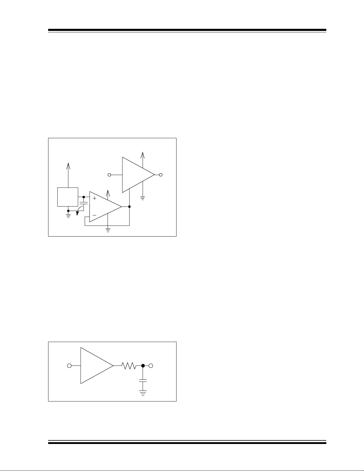
Figure 6-2 can be used. A small series resistor (R
at the V
load resistive at high frequencies. It will not, however,
improve the bandwidth.
improves the phase margin by making the
OUT
REF
V
pin at
OUT
ISO
For CL≥ 100 pF, a good estimate for R
value can be fine-tuned on the bench. Adjust R
is 50Ω. This
ISO
ISO
so
that the step response overshoot and frequency
response peaking are acceptable at all gains.
6.3 Layout Considerations
Good PC board layout techniques will help achieve the
performance shown in the Electrical Characteristics
and Typical Performance Curves. It will also help
minimize EMC (Electro-Magnetic Compatibility) issues.
6.3.1 COMPONENT PLACEMENT
Separate circuit functions; digital from analog, low
speed from high speed, and low power from high
power, as this will reduce crosstalk.
Keep sensitive traces short and straight, separating
them from interfering components and traces. This is
especially important for high frequency (low rise time)
signals.
Use a 0.1 µF supply bypass capacitor within 0.1 inch
(2.5 mm) of the V
ground plane. A multi-layer ceramic chip capacitor, or
high-frequency equivalent, works best.
6.3.2 SIGNAL COUPLING
The input pins of the MCP6S21/2/6/8 family of operational amplifiers (op amps) are high-impedance. This
makes them especially susceptible to capacitively-coupled noise. Using a ground plane helps reduce this
problem.
When noise is capacitively-coupled, the ground plane
provides additional shunt capacitance to ground. When
noise is magnetically coupled, the ground plane
reduces the mutual inductance between traces.
Increasing the separation between traces makes a
significant difference.
Changing the direction of one of the traces can also
reduce magnetic coupling. It may help to locate guard
)
traces next to the victim trace. They should be on both
sides of the victim trace and be as close as possible.
Connect the guard traces to the ground plane at both
ends, and in the middle, of long traces.
pin. It must connect directly to the
DD
6.3.3 HIGH FREQUENCY ISSUES
R
ISO
V
IN
MCP6S2X
V
OUT
C
L
FIGURE 6-2: PGA Circuit for Large Capacitive Loads.
2003 Microchip Technology Inc. DS21117A-page 25
Because the MCP6S21/2/6/8 PGAs reach unity gain
near 64 MHz when G = 16 and 32, it is important to use
good PCB layout techniques. Any parasitic coupling at
high frequency might cause undesired peaking. Filtering high frequency signals (i.e., fast edge rates) can
help. To minimize high frequency problems:
• Use complete ground and power planes
• Use HF, surface mount components
• Provide clean supply voltages and bypassing
• Keep traces short and straight
• Try a linear power supply (e.g., an LDO)

MCP6S21/2/6/8
6.4 Typical Applications
6.4.1 GAIN RANGING
Figure 6-3 shows a circuit that measures the current IX.
It benefits from changing the gain on the PGA. Just as
a hand-held multimeter uses different measurement
ranges to obtain the best results, this circuit makes it
easy to set a high gain for small signals and a low gain
for large signals. As a result, the required dynamic
range at the PGA’s output is less than at its input (by up
to 30 dB).
MCP6S2X
I
X
R
S
FIGURE 6-3: Wide Dynamic Range Current Measurement Circuit.
6.4.2 SHIFTED GAIN RANGE PGA
Figure 6-4 shows a circuit using an MCP6021 at a gain
of +10 in front of an MCP6S21. This changes the overall gain range to +10 V/V to +320 V/V (from +1 V/V to
+32 V/V).
V
OUT
V
IN
+
MCP6021
_
1.11 kΩ
10.0 kΩ
MCP6S21
V
OUT
FIGURE 6-5: PGA with lower gain range.
6.4.3 EXTENDED GAIN RANGE PGA
Figure 6-6 gives a +1 V/V to +1024 V/V gain range,
which is much greater than the range for a single PGA
(+1 V/V to +32 V/V). The first PGA provides input multiplexing capability, while the second PGA only needs
one input. These devices can be daisy chained
(Section 5.3, “Daisy Chain Configuration”).
V
IN
MCP6S28
MCP6S21
V
OUT
V
IN
+
MCP6021
_
10.0 kΩ
1.11 kΩ
MCP6S21
V
OUT
FIGURE 6-4: PGA with Modified Gain Range.
It is also easy to shift the gain range to lower gains (see
Figure 6-6). The MCP6021 acts as a unity gain buffer,
and the resistive voltage divider shifts the gain range
down to +0.1 V/V to +3.2 V/V (from +1 V/V to +32 V/V).
FIGURE 6-6: PGA with Extended Gain Range.
6.4.4 MULTIPLE SENSOR AMPLIFIER
The multiple channel PGAs (except the MCP6S21)
allow the user to select which sensor appears on the
output (see Figure 6-7). These devices can also
change the gain to optimize performance for each
sensor.
Sensor # 0
Sensor # 1
Sensor # 5
MCP6S26
V
OUT
FIGURE 6-7: PGA with Multiple Sensor Inputs.
DS21117A-page 26 2003 Microchip Technology Inc.

MCP6S21/2/6/8
6.4.5 EXPANDED INPUT PGA
Figure 6-8 shows cascaded MCP6S28s that provide
up to 15 input channels. Obviously, Sensors #7-14
have a high total gain range available, as explained in
Section 6.4.3, “Extended Gain Range”. These devices
can be daisy chained (Section 5.3, “Daisy Chain
Configuration”).
Sensors
# 0-6
Sensors
# 7-14
MCP6S28
MCP6S28
V
OUT
FIGURE 6-8: PGA with Expanded Inputs.
®
6.4.6 PICmicro
MCU WITH EXPANDED
INPUT CAPABILITY
Figure 6-9 shows an MCP6S28 driving an analog input
to a PICmicro
the input capacity of the microcontroller, while adding
the ability to select the appropriate gain for each
source.
®
microcontroller. This greatly expands
6.4.7 ADC DRIVER
The family of PGA’s is well suited for driving Analog-toDigital Converters (ADC). The binary gains (1, 2, 4, 8,
16 and 32) effectively add five more bits to the input
range (see Figure 6-10). This works well for applications needing relative accuracy more than absolute
accuracy (e.g., power monitoring).
Lowpass
Filter
V
IN
MCP6S28
MCP3201
12
OUT
FIGURE 6-10: PGA as an ADC Driver.
At low gains, the ADC’s Signal-to-Noise Ratio (SNR)
will dominate since the PGAs input noise voltage density is so low (10 nV/√Hz @ 10 kHz, typ.). At high gains,
the PGA’s noise will dominate the SNR, but its low
noise supports most applications. Again, these PGAs
add the flexibility of selecting the best gain for an
application.
The low pass filter in the block diagram reduces the
integrated noise at the MCP6S28’s output and serves
as an anti-aliasing filter. This filter may be designed
using Microchip’s FilterLab
www.microchip.com.
®
software, available at
V
IN
MCP6S28
PICmicro
Microcontroller
SPI™
®
FIGURE 6-9: Expanded Input for a PICmicro Microcontroller.
2003 Microchip Technology Inc. DS21117A-page 27
MCP6S21/2/6/8
7.0 PACKAGING INFORMATION
7.1 Package Marking Information
8-Lead PDIP (300 mil) (MCP6S21, MCP6S22)
XXXXXXXX
XXXXXNNN
YYWW
8-Lead SOIC (150 mil) (MCP6S21, MCP6S22)
XXXXXXXX
XXXXYYWW
NNN
8-Lead MSOP (MCP6S21, MCP6S22)
XXXXX
YWWNNN
Example:
MCP6S21
I/P256
0345
Example:
MCP6S21
I/SN0345
256
Example:
MCP6S21I
345256
Legend: XX...X Customer specific information*
YY Year code (last 2 digits of calendar year)
WW Week code (week of January 1 is week ‘01’)
NNN Alphanumeric traceability code
Note: In the event the full Microchip part number cannot be marked on one line, it will
be carried over to the next line thus limiting the number of available characters
for customer specific information.
* Standard marking consists of Microchip part number, year code, week code, traceability code (facility
code, mask rev#, and assembly code). For marking beyond this, certain price adders apply. Please check
with your Microchip Sales Office.
DS21117A-page 28 2003 Microchip Technology Inc.

Package Marking Information (Con’t)
14-Lead PDIP (300 mil) (MCP6S26)Example:
MCP6S21/2/6/8
XXXXXXXXXXXXXX
XXXXXXXXXXXXXX
YYWWNNN
14-Lead SOIC (150 mil) (MCP6S26)
XXXXXXXXXXX
XXXXXXXXXXX
YYWWNNN
14-Lead TSSOP (4.4mm) (MCP6S26)
XXXXXXXX
YYWW
NNN
MCP6S26-I/P
XXXXXXXXXXXXXX
0345256
Example:
MCP6S26ISL
XXXXXXXXXXXXXXXXXXXXXXXXX
0345256
Example:
MCP6S26IST
0345
256
2003 Microchip Technology Inc. DS21117A-page 29

MCP6S21/2/6/8
Package Marking Information (Con’t)
16-Lead PDIP (300 mil) (MCP6S28)Example:
XXXXXXXXXXXXXX
XXXXXXXXXXXXXX
YYWWNNN
16-Lead SOIC (150 mil) (MCP6S28)
XXXXXXXXXXXXX
XXXXXXXXXXXXX
YYWWNNN
MCP6S28-I/P
XXXXXXXXXXXXXX
0345256
Example:
MCP6S28-I/SL
XXXXXXXXXXXXXXXXXXXXXXXX
0345256
DS21117A-page 30 2003 Microchip Technology Inc.

8-Lead Plastic Dual In-line (P) – 300 mil (PDIP)
E1
D
2
MCP6S21/2/6/8
n
E
β
eB
Number of Pins
Pitch
Top to Seating Plane A .140 .155 .170 3.56 3.94 4.32
Molded Package Thickness A2 .115 .130 .145 2.92 3.30 3.68
Base to Seating Plane A1 .015 0.38
Shoulder to Shoulder Width E .300 .313 .325 7.62 7.94 8.26
Molded Package Width E1 .240 .250 .260 6.10 6.35 6.60
Overall Length D .360 .373 .385 9.14 9.46 9.78
Tip to Seating Plane L .125 .130 .135 3 .18 3.30 3.43
Lead Thickness
Upper Lead Width B1 .045 .058 .070 1.14 1.46 1.78
Lower Lead Width B .014 .018 .022 0.36 0.46 0.56
Overall Row Spacing § eB .310 .370 .430 7.87 9.40 10.92
Mold Draft Angle Top
Mold Draft Angle Bottom
* Controlling Parameter
§ Significant Characteristic
Notes:
Dimensions D and E1 do not include m old flash or protrusions. Mold flash or protrusions shall not exceed
.010” (0.254mm) per side.
JEDEC Equivalent: MS-001
Drawing No. C04-018
Dimension Limits MIN NOM MAX MIN NOM MAX
1
α
A
c
Units INCHES* MILLIMETERS
n
p
c
α
β
.008 .012 .015 0.20 0.29 0.38
A1
B1
B
88
.100 2.54
51015 51015
51015 51015
A2
L
p
2003 Microchip Technology Inc. DS21117A-page 31

MCP6S21/2/6/8
8-Lead Plastic Small Outline (SN) – Narrow, 150 mil (SOIC)
E
E1
p
D
2
B
Number of Pins
Pitch
Foot Angle
Lead Thickness
Mold Draft Angle Top
Mold Draft Angle Bottom
* Controlling Paramete r
§ Significant Characteristic
Notes:
Dimensions D and E1 do not include mold flash or protrusions. Mold flash or protrusions shall not exceed
.010” (0.254mm) per side.
JEDEC Equivalent: MS-012
Drawing No. C04-057
n
45°
c
β
n
p
φ
c
α
β
1
h
A
φ
L
048048
A1
MILLIMETERSINCHES*Units
1.27.050
α
A2
MAXNOMMINMAXNOMMINDimension Limits
88
1.751.551.35.069.061.053AOverall Height
1.551.421.32.061.056.052A2Molded Package Thickness
0.250.180.10.010.007.004A1Standoff §
6.206.025.79.244.237.228EOverall Width
3.993.913.71.157.154.146E1Molded Package W idth
5.004.904.80.197.193.189DOverall Length
0.510.380.25.020.015.010hChamfer Distance
0.760.620.48.030.025.019LFoot Length
0.250.230.20.010.009.008
0.510.420.33.020.017.013BLead Width
1512015120
1512015120
DS21117A-page 32 2003 Microchip Technology Inc.

8-Lead Plastic Micro Small Outline Package (MS) (MSOP)
MCP6S21/2/6/8
p
B
n 1
c
(F)
β
Dimension Limits
Number of Pins
Pitch
Overall Height
Molded Package Thickness
Standoff §
Overall Width
Molded Package Width
Overall Length
Foot Length
Foot Angle
Lead Thickness
Lead Width
Mold Draft Angle Top
Mold Draft Angle Bottom
*Controlling Parameter
§ Significant Characteristic
Notes:
Dimensions D and E1 do not include mold flash or protrusions. Mold flash or protrusions shall not
exceed .010" (0.254mm ) per side.
E1
E
D
2
A
Units
n
p
A
A2
A1
E
E1
D
L
φ
c
B
α
β
MIN
.030
.002
.184
.114
.114
.016
.004
.010
φ
L
INCHES
NOM
.026
.034
.193
.118
.118
.022
.037.035FFootprint (Reference)
0
.006
.012
A1
8
.044
.038
.006
.200
.122
.122
.028
6
.008
.016
7
7
MILLIMETERS*
MINMAX NOM
0.65
0.76
0.05
4.67
2.90
2.90
0.40
0
0.10
0.25
0.86
4.90
3.00
3.00
0.55
0.15
0.30
α
A2
MAX
8
1.18
0.97
0.15
.5.08
3.10
3.10
0.70
1.000.950.90.039
6
0.20
0.40
7
7
Drawing No. C04-111
2003 Microchip Technology Inc. DS21117A-page 33
MCP6S21/2/6/8
14-Lead Plastic Dual In-line (P) – 300 mil (PDIP)
E1
D
2
n
E
β
eB
Number of Pins
Pitch
Top to Seating Plane A .140 .155 .170 3.56 3.94 4.32
Molded Package Thickness A2 .115 .130 .145 2.92 3.30 3.68
Base to Seating Plane A1 .015 0.38
Shoulder to Shoulder Width E .300 .313 .325 7.62 7.94 8.26
Molded Package Width E1 .240 .250 .260 6.10 6.35 6.60
Overall Length D .740 .750 .760 18.80 19.05 19.30
Tip to Seating Plane L .125 .130 .135 3 .18 3.30 3.43
Lead Thickness
Upper Lead Width B1 .045 .058 .070 1.14 1.46 1.78
Lower Lead Width B .014 .018 .022 0.36 0.46 0.56
Overall Row Spacing § eB .310 .370 .430 7.87 9.40 10.92
Mold Draft Angle Top
Mold Draft Angle Bottom
* Controlling Parameter
§ Significant Characteristic
Notes:
Dimensions D and E1 do not include m old flash or protrusions. Mold flash or protrusions shall not exceed
.010” (0.254mm) per side.
JEDEC Equivalent: MS-001
Drawing No. C04-005
1
A
c
A1
Dimension Limits MIN NOM MAX MIN NOM MAX
Units INCHES* MILLIMETERS
n
p
c
α
β
.008 .012 .015 0.20 0.29 0.38
5 10 15 5 10 15
5 10 15 5 10 15
B1
B
14 14
.100 2.54
α
A2
L
p
DS21117A-page 34 2003 Microchip Technology Inc.
14-Lead Plastic Small Outline (SL) – Narrow, 150 mil (SOIC)
E
E1
p
D
2
B
n
1
MCP6S21/2/6/8
45°
c
β
Number of Pins
Pitch
Foot Angle
Lead Thickness
Mold Draft Angle Top
Mold Draft Angle Bottom
* Controlling Paramete r
§ Significant Characteristic
Notes:
Dimensions D and E1 do not include mold flash or protrusions. Mold flash or protrusions shall not exceed
.010” (0.254mm) per side.
JEDEC Equivalent: MS-012
Drawing No. C04-065
h
A
φ
L
n
p
φ
c
α
β
A1
048048
α
MILLIMETERSINCHES*Units
1.27.050
A2
MAXNOMMINMAXNOMMINDimension Limits
1414
1.751.551.35.069.061.053AOverall Height
1.551.421.32.061.056.0 52A2Molded Package Thickness
0.250.180.10.010.007.004A1Standoff §
6.205.995.79.244.236.228EOverall Width
3.993.903.81.157.154.150E1Molded Package Width
8.818.698.56.347.34 2.337DOverall Length
0.510.380.25.020.015.010hChamfer Distance
1.270.840.41.050.033.016LFoot Length
0.250.230.20.010.009.008
0.510.420.36.020.017.014BLead Width
1512015120
1512015120
2003 Microchip Technology Inc. DS21117A-page 35

MCP6S21/2/6/8
14-Lead Plastic Thin Shrink Small Outline (ST) – 4.4 mm (TSSOP)
E
E1
p
D
2
n
B
1
A
c
φ
β
Number of Pins
Pitch
Foot Angle
Lead Thickness
Mold Draft Angle Top
Mold Draft Angle Bottom
* Controlling Parameter
§ Significant Characteristic
Notes:
Dimensions D and E1 do not include mo ld flash or protrusions. Mold flash or protrusions shall not exceed
.005” (0.127mm) per side.
JEDEC Equivalent: MO-153
Drawing No. C04-087
n
p
φ
c
α
β
L
MILLIMETERS*INCHESUnits
0.65.026
α
A2A1
MAXNOMMINMAXNOMMINDimension Limits
1414
1.10.043AOverall Height
0.950.900.85.037.035.033A2Molded Package Thickness
0.150.100.05.006.004.002A1Standoff §
6.506.386.25.256.251.246EOverall Width
4.504.404.30.177.173.169E1Molded Package Width
5.105.004.90.201.197.193DMolded Package Length
0.700.600.50.028.024.020LFoot Length
840840
0.200.150.09.008.006.004
0.300.250.19.012.010.007B1Lead Width
10501050
10501050
DS21117A-page 36 2003 Microchip Technology Inc.

16-Lead Plastic Dual In-line (P) – 300 mil (PDIP)
E1
D
MCP6S21/2/6/8
2
n
E
β
eB
Number of Pins
Pitch
Molded Package Thickness
Lead Thickness
Overall Row Spacing §
Mold Draft Angle Top
Mold Draft Angle Bottom
* Controlling Parameter
§ Significant Characteristic
Notes:
Dimensions D and E1 do not include mold flash or protrusions. Mold flash or protrusions shall not exceed
.010” (0.254mm) per side.
JEDEC Equivalent: MS-001
Drawing No. C04-017
1
A
c
A1
n
p
A2
c
eB
α
β
B1
B
0.38.015A1Base to Seating Plane
α
p
MILLIMETERSINCHES*Units
2.54.100
A2
L
MAXNOMMINMAXNOMMINDimension Limits
1616
4.323.943.56.170.155.140ATop to Seating Plane
3.683.302.92.145.130.115
8.267.947.62.325.313.300EShoulder to Shoulder Widt h
6.606.356.10.260.250.240E1Molded Package Width
19.3019.0518.80.760.750.740DOverall Length
3.433.303.18.135.130.125LTip to Seating Plane
0.380.290.20.015.012.008
1.781.461.14.070.058.045B1Upper Lead Width
0.560.46.036.022.018.014BLower Lead Width
10.929.407.87.430.370.310
1510515105
1510515105
2003 Microchip Technology Inc. DS21117A-page 37

MCP6S21/2/6/8
16-Lead Plastic Small Outline (SL) – Narrow 150 mil (SOIC)
E
E1
p
D
2
B
n
45°
1
h
α
c
φ
L
β
Number of Pins
Pitch
Foot Angle
Lead Thickness
Mold Draft Angle Top
Mold Draft Angle Bot tom
* Controlling Parameter
§ Significant Cha racteristic
Notes:
Dimensions D and E1 do not include m old flash or protrusions. Mold flash or protrusions shall not exceed
.010” (0.254mm) per side.
JEDEC Equivalent: MS-012
Drawing No. C04-108
n
p
φ
c
α
β
A
A1
MILLIMETERSINCHES*Units
048048
A2
MAXNOMMINMAXNOMMINDimension Limits
1616
1.27.050
1.751.551.35.069.061.053AOverall Height
1.551.441.32.061.057.052A2Molded Package Thickness
0.250.180.10.010.007.004A1Standoff §
6.206.025.79.244.237.228EOverall Width
3.993.903.81.157.154.150E1Molded Package Width
10.019.919.80.394.390.386DOverall Length
0.510.380.25.020.015.010hChamfer Distance
1.270.840.41.050.033.016LFoot Length
0.250.230.20.010.009.008
0.510.420.33.020.017.013BLead Width
1512015120
1512015120
DS21117A-page 38 2003 Microchip Technology Inc.

NOTES:
MCP6S21/2/6/8
2003 Microchip Technology Inc. DS21117A-page 39

MCP6S21/2/6/8
PRODUCT IDENTIFICATION SYSTEM
To order or obtain information, e.g., on pricing or delivery, refer to the factory or the listed sales office.
PART NO. -X /XX
Device
PackageTe mpe ratu re
Range
Device: MCP6S21: One Channel PGA
Temperature Range: I = -40°C to +85°C
Package: MS = Plastic Micro Small Outline (MSOP), 8-lead
MCP6S21T: One Channel PGA
MCP6S22: Two Channel PGA
MCP6S22T: Two Channel PGA
MCP6S26: Six Channel PGA
MCP6S26T: Six Channel PGA
MCP6S28: Eight Cha nnel PGA
MCP6S28T: Eight Channel PGA
P = Plastic DIP (300 mil Body), 8, 14, and 16-lead
SN = Plastic SOIC, (150 mil Body), 8-lead
SL = Plastic SOIC (150 mil Body), 14, 16-lead
ST = Plastic TSSOP (4.4mm B ody), 14-lead
(Tape and Reel for SOIC and MSOP)
(Tape and Reel for SOIC and MSOP)
(Tape and Reel for SOIC and TSSOP)
(Tape and Reel for SOIC)
Examples:
a) MCP6S21-I/P: One Channel PGA,
PDIP package.
b) MCP6S21-I/SN: One Channe l PGA,
SOIC package .
c) MCP6S21-I/MS: One Channel PGA,
MSOP package.
d) MCP6S22-I/MS: Two Channel PGA,
MSOP package.
e) MCP6S22T-I/MS: Tape and Reel,
Two Channel PGA, MSOP package.
f) MCP6S26-I/P: Six Channel PGA,
PDIP package.
g) MCP6S26-I/SN: Six Channel PG A,
SOIC package .
h) MCP6S26T-I/ST: Tape and Reel,
Six Channel PGA, TSSOP package.
i) MCP6S28T-I/SL: Tape and Reel,
Eight Chann el PGA, SOIC package.
Sales and Support
Data Sheets
Products supported by a preliminary Data Sheet may have an errata sheet describing minor operational differences and recommended workarounds. To determine if an errata sheet exists for a particular device, please contact one of the following:
1. Your local Microchip sales office
2. The Microchip Corporate Literature Center U.S. FAX: (480) 792-7277
3. The Microchip Worldwide Site (www.microchip.com)
Please specify which device, revision of silicon and Data Sheet (include Literature #) you are using.
New Customer Notification System
Register on our web site (www.microchip.com/cn) to receive the most current information on our products.
2002 Microchip Technology Inc. DS21117A-page 39

MCP6S21/2/6/8
NOTES:
DS21117A-page 40 2002 Microchip Technology Inc.

Note the following details of the code protection feature on Microchip devices:
• Microchip products meet the specification contained in their particular Microchip Data Sheet.
• Microchip believes that its family of products is one of the most secure families of its kind on the market today, when used in the
intended manner and under normal conditions.
• There are dishonest and possibly illegal methods used to breach the code protection feature. All of these methods, to our
knowledge, require using the Microchip products in a manner outside the operating specifications contained in Microchip's Data
Sheets. Most likely, the person doing so is engaged in theft of intellectual property.
• Microchip is willing to work with the customer who is concerned about the integrity of their code.
• Neither Microchip nor any other semiconductor manufacturer can guarantee the security of their code. Code protection does not
mean that we are guaranteeing the product as “unbreakable.”
Code protection is constantly evolving. We at Microchip are committed to continuously improving the code protection features of our
products. Attempts to break microchip’s code protection feature may be a violation of the Digital Millennium Copyright Act. If such
acts allow unauthorized access to your software or other copyrighted work, you may have a right to sue for relief under that Act.
Information contained in this publication regarding device
applications and the like is intended through suggestion only
and may be superseded by updates. It is your responsibility to
ensure that your application meets with your specifications. No
representation or warranty is given and no liability is assumed
by Microchip Technology Incorporated with respect to the
accuracy or use of such information, or infringement of patents
or other intellectual property rights arising from such use or
otherwise. Use of Microchip’s products as critical components in
life support systems is not authorized except with express
written approval by Microchip. No licenses are conveyed,
implicitly or otherwise, under any intellectual property rights.
Trademarks
The Microchip name and logo, the Micr ochip logo, K
EELOQ
,
MPLAB, PIC, PICmicro, PICSTART, PRO MATE and
PowerSmart are registered trademarks of Microchip Technology
Incorporated in the U.S.A. and other countries.
FilterLab, microID, MXDEV, MXLAB, PICMASTER, SEEVAL
and The Embedded Control Solutions Company are registered
trademarks of Microchip Technology Incorporated in the U.S.A.
Accuron, Application Maestro, dsPIC, dsPICDEM,
dsPICDE M.net, ECONOMONITOR, FanSense, FlexROM,
fuzzyLAB, In-Circuit Serial Programming, ICSP, ICEPIC,
microPort, Migratable Memory, MPASM, MPLIB, MPLINK,
MPSIM, PICC, PICkit, PICDEM, PICDEM.net, PowerCal,
PowerInfo, PowerMate, PowerTool, rfLAB, rfPIC, Select Mode,
SmartSensor, SmartShunt, SmartTel and Total Endurance are
trademarks of Microchip Technology Incorporated in the U.S.A.
and other countries.
Serialized Quick Turn Programming (SQTP) is a service mark of
Microchip Technology Incorporated in the U.S.A.
All other trademarks mentioned herein are property of their
respective companies.
© 2003, Microchip Technology Incorporated, Printed in the
U.S.A., All Rights Reserved.
Printed on recycled pape r.
Microchip received QS-9000 quality system
certification for its worldwide headquarters,
design and wafer fabrication facilities in
Chandler and Tempe, Arizona in July 1999
and Mountain View, California in March 2002.
The Company’s quality system processes and
procedures are QS-9000 compliant for its
PICmicro
devices, Serial EEPROMs, microperipherals,
non-volatile memory and analog produ cts. In
addition, Microchip’s qua lity system for the
design and manufacture of development
systems is ISO 9001 certified.
®
8-bit MCUs, KEEL
®
code hopping
OQ
2003 Microchip Technology Inc. DS21117A - page 41

M
W
ORLDWIDE SALES AND SERVICE
AMERICAS
Corporate Office
2355 West Chandler B lvd.
Chandler, AZ 85224-6199
Tel: 480-792-7200 Fax: 480-792-7277
Technical Support: 480-792-7627
Web Address: http://www.microchip.com
Rocky Mountain
2355 West Chandler B lvd.
Chandler, AZ 85224-6199
Tel: 480-792-7966 Fax: 480-792-4338
Atlanta
3780 Mansell Road, Suite 130
Alpharetta, GA 30022
Tel: 770-640-0034 Fax: 770-640-0307
Boston
2 Lan Drive, Suit e 120
Westford, MA 01886
Tel: 978-692-3848 Fax: 978-692-3821
Chicago
333 Pierce Road, S uite 180
Itasca, IL 60143
Tel: 630-285-0071 Fax: 630-285-0075
Dallas
4570 Westgrove Drive, Suite 160
Addison, TX 75001
Tel: 972-818-7423 Fax: 972-818-2924
Detroit
Tri-Atria Office Building
32255 Northwestern Highway, Suite 190
Farmington Hills, MI 48334
Tel: 248-538-2250 Fax: 248-538-2260
Kokomo
2767 S. Albright Road
Kokomo, Indiana 46902
Tel: 765-864-8360 Fax: 765-864-8387
Los Angeles
18201 Von Karman, Suite 10 90
Irvine, CA 92612
Tel: 949-263-1888 Fax: 949-263-1338
San Jose
Microchip Technology Inc.
2107 North First S treet, Suite 590
San Jose, CA 95131
Tel: 408-436-7950 Fax: 408-436-7955
Toro nto
6285 Northam Drive, Suite 108
Mississauga, Ontario L4V 1X5, Canada
Tel: 905-673-0699 Fax: 905-673-6509
ASIA/PACIFIC
Australia
Microchip Technology Australia Pty Ltd
Marketing Support Division
Suite 22, 41 Rawson Street
Epping 2121, NSW
Australia
Tel: 61-2-9868-6733 Fax: 61-2-9868-6755
China - Beijing
Microchip Technology Consulting (Shanghai)
Co., Ltd., Beijing Liaison Office
Unit 915
Bei Hai Wan Tai Bldg.
No. 6 Chaoyangmen Beidajie
Beijing, 100027, No. China
Tel: 86-10-852821 00 Fax: 86-10-852 82104
China - Chengdu
Microchip Technology Consulting (Shanghai)
Co., Ltd., Chengdu Liaison Office
Rm. 2401-2402, 24th Floor,
Ming Xing Financial Tower
No. 88 TIDU Street
Chengdu 610016, China
Tel: 86-28-867662 00 Fax: 86-28-867 66599
China - Fuzhou
Microchip Technology Consulting (Shanghai)
Co., Ltd., Fuzhou Liaison Office
Unit 28F, World Trade Plaza
No. 71 Wusi Road
Fuzhou 350001, China
Tel: 86-591-75035 06 Fax: 86-591-7503521
China - Hong Kong SAR
Microchip Technology Hongkong Ltd.
Unit 901-6, Tower 2, Metroplaza
223 Hing Fong Road
Kwai Fong, N.T., Hong Kong
Tel: 852-2401-120 0 Fax: 852-2401-3431
China - Shanghai
Microchip Technology Consulting (Shanghai)
Co., Ltd.
Room 701, Bldg. B
Far East International Plaza
No. 317 Xian Xia Road
Shanghai, 200051
Tel: 86-21-6275-5700 Fax: 86-21-6275-5060
China - Shenzhen
Microchip Technology Consulting (Shanghai)
Co., Ltd., Shenzhen L iaison Office
Rm. 1812, 18/F, Building A, United Plaza
No. 5022 Binhe Road, Futian District
Shenzhen 518033, Ch ina
Tel: 86-755-82901 380 Fax: 86-755-82966626
China - Qingdao
Rm. B505A, Fullhope Plaza,
No. 12 Hong Kong Central Rd.
Qingdao 266071, China
Tel: 86-532-50273 55 Fax: 86-532-5027205
India
Microchip Technology Inc.
India Liaison Office
Marketing Support Division
Divyasree Chambers
1 Floor, Wing A (A3/A4)
No. 11, O’Shaugnessey Road
Bangalore, 560 025, India
Tel: 91-80-229006 1 Fax: 91-80-2290 062
Japan
Microchip Technology Japan K.K.
Benex S-1 6F
3-18-20, Shinyokohama
Kohoku-Ku, Yokohama-shi
Kanagawa, 222-0033, Japan
Tel: 81-45-471- 6166 Fax: 81-45-471-6122
Korea
Microchip Technology Korea
168-1, Youngbo Bldg. 3 Floor
Samsung-Dong, Kangnam-Ku
Seoul, Korea 135-882
Tel: 82-2-554-7200 Fax: 82-2-558-593 4
Singapore
Microchip Technology Singapore Pte Ltd.
200 Middle Road
#07-02 Prime Centre
Singapore, 188980
Tel: 65-6334-8870 Fax: 65-6334-8850
Ta iw an
Microchip Technology (Barbados) Inc.,
Taiwan Branch
11F-3, No. 207
Tung Hua North Road
Taipei, 105, Taiwan
Tel: 886-2-2717-7175 Fax: 886-2-2545-0139
EUROPE
Austria
Microchip Technology Austria GmbH
Durisolstrasse 2
A-4600 Wels
Austria
Tel: 43-7242-2244-399
Fax: 43-7242-2244-393
Denmark
Microchip Technology Nordic ApS
Regus Business Centre
Lautrup hoj 1-3
Ballerup DK-2750 Denmark
Tel: 45 4420 9895 Fax: 45 4420 9910
France
Microchip Technology SARL
Parc d’Activite du Moulin de Massy
43 Rue du Saule Trapu
Batiment A - ler Etage
91300 Massy, France
Tel: 33-1-69-53-63-20 Fax: 33-1-69-30-90-79
Germany
Microchip Technology GmbH
Steinheilstrasse 10
D-85737 Ismaning, Germany
Tel: 49-089-627-144-100
Fax: 49-089-627-144-44
Italy
Microchip Technology SRL
Via Quasimodo, 12
20025 Legnano (MI)
Milan, Italy
Tel: 39-0331-742611 Fax: 39-0331-466781
United Kingdom
Microchip Ltd.
505 Eskdale Road
Winnersh Triangle
Wokingham
Berkshire, England RG41 5TU
Tel: 44 118 921 5869 Fax: 44-118 921-5820
02/12/03
DS21117A-page 42 2003 Microchip Technology Inc.
 Loading...