

MCP6546/6R/6U/7/8/9
Open-Drain Output Sub-Microamp Comparators
Features
• Low Quiescent Current: 600 nA/comparator (typ.)
• Rail-to-Rail Input: V
• Open-Drain Output: V
- 0.3V to V
SS
OUT
≤ 10V
DD
+ 0.3V
• Propagation Delay: 4 µs (typ., 100 mV Overdrive)
• Wide Supply Voltage Range: 1.6V to 5.5V
• Single available in SOT-23-5, SC-70-5 * packages
• Available in Single, Dual and Quad
• Chip Select (CS
) with MCP6548
• Low Switching Current
• Internal Hysteresis: 3.3 mV (typ.)
• Temperature Range:
- Industrial: -40°C to +85°C
- Extended: -40°C to +125°C
Typical Applications
• Laptop Computers
• Mobile Phones
• Metering Systems
• Hand-held Electronics
• RC Timers
• Alarm and Monitoring Circuits
• Windowed Comparators
• Multi-vibrators
Description
The Microchip Technology Inc. MCP6546/7/8/9 family
of comparators is offered in single (MCP6546,
MCP6546R, MCP6546U), single with chip select
(MCP6548), dual (MCP6547) and quad (MCP6549)
configurations. The outputs are open-drain and are
capable of driving heavy DC or capacitive loads.
These comparators are optimized for low power,
single-supply application with greater than rail-to-rail
input operation. The output limits supply current surges
and dynamic power consumption while switching. The
open-drain output of the MCP6546/7/8/9 family can be
used as a level-shifter for up to 10V using a pull-up
resistor. It can also be used as a wired-OR logic. The
internal Input hysteresis eliminates output switching
due to internal noise voltage, reducing current draw.
These comparators operate with a single-supply
voltage as low as 1.6V and draw a quiescent current of
less than 1 µA/comparator.
The related MCP6541/2/3/4 family of comparators from
Microchip has a push-pull output that supports rail-torail output swing and interfaces with CMOS/TTL logic.
* SC-70-5 E-Temp parts not avaliable at this release
the data sheet
.
MCP6546U SOT-23-5 is E-Temp only.
of
Related Devices
• CMOS/TTL-Compatible Output: MCP6541/2/3/4
Package Types
MCP6546
PDIP, SOIC, MSOP
1
NC
V
IN
VIN+
V
SS
2
–
+
3
4
8
7
6
5
NC
V
DD
OUT
NC
OUT
V
MCP6546
SOT-23-5, SC-70-5
V
OUT
1
V
2
SS
V
+
3
IN
© 2006 Microchip Technology Inc. DS21714E-page 1
5
+
-
4
DD
VIN–
VIN–
V
MCP6546R MCP6547
SOT-23-5
OUTA
1
V
DD
+
IN
+
2
3
V
5
SS
V
-
4
VIN–
INA
V
INA
V
MCP6546U
SOT-23-5
1
V
SS
+
IN
+
2
3
V
5
DD
V
OUT
4
V
V
PDIP, SOIC, MSOP
SS
1
–
-
2
+
3
4
8
+
7
+
-
6
5
MCP6548
PDIP, SOIC, MSOP
NC
IN
IN
SS
1
2
–
+
+
3
4
8
7
6
5
V
DD
OUTB
V
INB
V
INB
CS
V
DD
OUT
NC
–
+
OUTA
V
INA
V
INA
V
V
INB
V
INB
OUTB
MCP6549
PDIP, SOIC, TSSOP
14
+
13
+
-
12
11
10
-
+
+
9
8
DD
1
2
-
–
3
+
4
+
5
-
–
6
7
OUTD
V
IND
V
IND
V
SS
V
INC
V
INC
OUTC
–
+
+
–
MCP6546/6R/6U/7/8/9
1.0 ELECTRICAL CHARACTERISTICS
Absolute Maximum Ratings †
VDD - VSS.........................................................................7.0V
Open-Drain output............................................... V
Analog Input (V
All other inputs and outputs ........... V
+, VIN-)††............. VSS - 1.0V to VDD + 1.0V
IN
– 0.3V to VDD + 0.3V
SS
Difference Input voltage ...................................... |V
+ 10.5V
SS
DD
– VSS|
† Notice: Stresses above those listed under “Absolute Maximum Ratings” may cause permanent damage to the device.
This is a stress rating only and functional operation of the
device at those or any other conditions above those indicated
in the operational listings of this specification is not implied.
Exposure to maximum rating conditions for extended periods
may affect device reliability.
†† See Section 4.1.2 “Input Voltage and Current
Limits”
Output Short-Circuit Current .................................continuous
Current at Input Pins ....................................................±2 mA
Current at Output and Supply Pins ............................±30 mA
Storage temperature .....................................-65°C to +150°C
Maximum Junction Temperature (T
) .......................... +150°C
J
ESD protection on all pins:
(HBM;MM) .....................................2 kV;200V (MCP6546U)
(HBM;MM) ................................ 4 kV; 200V (all other parts)
DC CHARACTERISTICS
Electrical Specifications: Unless otherwise indicated, VDD = +1.6V to +5.5V, VSS = GND, TA = 25°C, VIN+ = VDD/2, VIN– = VSS,
R
=2.74kΩ to VPU = VDD (Refer to Figure 1-3).
PU
Parameters Sym Min Typ Max Units Conditions
Power Supply
Supply Voltage V
Quiescent Current
(per comparator)
DD
I
Q
Input
Input Voltage Range V
CMRVSS
Common Mode Rejection Ratio CMRR 55 70 — dB V
Common Mode Rejection Ratio CMRR 50 65 — dB V
Common Mode Rejection Ratio CMRR 55 70 — dB V
Power Supply Rejection Ratio PSRR 63 80 — dB V
Input Offset Voltage V
Drift with Temperature ΔV
Input Hysteresis Voltage V
Linear Temp. Co. TC
Quadratic Temp. Co. TC
Input Bias Current I
At Temperature (I-Temp parts) I
At Temperature (E-Temp parts) I
Input Offset Current I
Common Mode Input Impedance Z
Differential Input Impedance Z
OS
OS
HYST
B
B
B
OS
CM
DIFF
/ΔT
1
2
Note 1: The input offset voltage is the center of the input-referred trip points. The input hysteresis is the difference between the
input-referred trip points.
2: V
at differential temperatures is estimated using: V
HYST
3: Input bias current at temperature is not tested for the SC-70-5 package
4: Do not short the output above V
V
test limit was VDD before Dec. 2004 (week code 52).
PU
1.6 — 5.5 V VPU ≥ V
0.3 0.6 1 µA I
− 0.3 — V
+ 0.3 V
DD
-7.0 ±1.5 +7.0 mV VCM = V
— ±3 — µV/°C TA = -40°C to +125°C, VCM = V
A
1.5 3.3 6.5 mV VCM = V
—6.7 —µV/°CT
— -0.035 — µV/°C2TA = -40°C to +125°C, VCM = V
—1 —pAV
— 25 100 pA TA = +85°C, VCM = V
— 1200 5000 pA TA = +125°C, VCM = V
— ±1 — pA V
DD
= 0
OUT
= 5V, VCM = -0.3V to 5.3V
DD
= 5V, VCM = 2.5V to 5.3V
DD
= 5V, VCM = -0.3V to 2.5V
DD
= V
CM
SS
(Note 1)
SS
SS
(Note 1)
SS
= -40°C to +125°C, VCM = VSS (Note 2)
A
(Note 2)
SS
CM = VSS
(Note 3)
SS
(Note 3)
SS
CM = VSS
—1013||4 — Ω||pF
—1013||2 — Ω||pF
(TA) = V
HYST
+ 10V. Limit the output current to Absolute Maximum Rating of 30 mA. The minimum
SS
+ (TA -25°C) TC1 + (TA - 25°C)2TC2.
HYST
DS21714E-page 2 © 2006 Microchip Technology Inc.
MCP6546/6R/6U/7/8/9
DC CHARACTERISTICS (CONTINUED)
Electrical Specifications: Unless otherwise indicated, VDD = +1.6V to +5.5V, VSS = GND, TA = 25°C, VIN+ = VDD/2, VIN– = VSS,
R
=2.74kΩ to VPU = VDD (Refer to Figure 1-3).
PU
Parameters Sym Min Typ Max Units Conditions
Open-Drain Output
Output Pull-Up Voltage V
High-Level Output Current I
Low-Level Output Voltage V
Short-Circuit Current I
Output Pin Capacitance C
OH
I
SC
OUT
PU
OL
SC
Note 1: The input offset voltage is the center of the input-referred trip points. The input hysteresis is the difference between the
input-referred trip points.
2: V
at differential temperatures is estimated using: V
HYST
3: Input bias current at temperature is not tested for the SC-70-5 package
4: Do not short the output above V
V
test limit was VDD before Dec. 2004 (week code 52).
PU
AC CHARACTERISTICS
Electrical Specifications: Unless otherwise indicated, V
Step = 200 mV, Overdrive = 100 mV, R
Parameters Sym Min Typ Max Units Conditions
Fall Time t
Propagation Delay (High-to-Low) t
Propagation Delay (Low-to-High) t
Propagation Delay Skew t
Maximum Toggle Frequency f
Input Noise Voltage E
Note 1: t
and t
R
depend on the load (RL and CL); these specifications are valid for the indicated load only.
PLH
2: Propagation Delay Skew is defined as: t
=2.74kΩ to VPU = VDD, and CL = 36 pF (Refer to Figure 1-2 and Figure 1-3).
PU
F
PHL
PLH
PDS
MAX
f
MAX
ni
1.6 — 10 V (Note 4)
-100 — — nA VDD = 1.6V to 5.5V, VPU = 10V (Note 4)
V
SS
—V
SS
+ 0.2 V I
= 2 mA, VPU = VDD = 5V
OUT
—±1.5 — mAVPU = VDD = 1.6V (Note 4)
–30—mAV
= VDD = 5.5V (Note 4)
PU
—8 —pF
(TA) = V
HYST
+ 10V. Limit the output current to Absolute Maximum Rating of 30 mA. The minimum
SS
= +1.6V to +5.5V, VSS = GND, TA = 25°C, VIN+ = VDD/2,
DD
+ (TA -25°C) TC1 + (TA - 25°C)2TC2.
HYST
—0.7—µs(Note 1)
—4.08.0µs
—3.08.0µs(Note 1)
—-1.0— µs(Notes 1 and 2)
— 225 — kHz VDD = 1.6V
— 165 — kHz VDD = 5.5V
— 200 — µV
= t
- t
PDS
PLH
PHL
.
10 Hz to 100 kHz
P-P
MCP6548 CHIP SELECT (CS) CHARACTERISTICS
Electrical Specifications: Unless otherwise indicated, VDD = +1.6V to +5.5V, VSS = GND, TA = 25°C, VIN+ = VDD/2, VIN– = VSS,
R
=2.74kΩ to VPU = VDD, and CL = 36 pF (Refer to Figures 1-1 and 1-3).
PU
Parameters Sym Min Typ Max Units Conditions
CS Low Specifications
Logic Threshold, Low V
CS
CS
Input Current, Low I
IL
CSL
CS High Specifications
Logic Threshold, High V
CS
CS
Input Current, High I
CS Input High, VDD Current I
CS Input High, GND Current I
Comparator Output Leakage I
Dynamic Specifications
CS
Low to Comparator Output Low
CS
Turn-on Time
CS High to Comparator Output
High Z Turn-off Time
CS Hysteresis V
IH
CSH
DD
SS
O(LEAK)
t
ON
t
OFF
CS_HYST
© 2006 Microchip Technology Inc. DS21714E-page 3
V
SS
—5—pACS = V
0.8 V
—1—pACS = V
—18—pACS = V
—-20—pACS = V
—1—pAV
— 0.2 V
—VDDV
DD
DD
V
SS
DD
DD
DD
= VSS+10V, CS = V
OUT
—250msCS = 0.2VDD to V
V
– = V
IN
DD
—10—µsCS = 0.8VDD to V
V
– = V
IN
DD
—0.6— VVDD = 5V
OUT
OUT
DD
= VDD/2,
= VDD/2,
MCP6546/6R/6U/7/8/9
V
t
IL
ON
CS
V
High-Z
OUT
I
-20 pA (typ.)
SS
I
1 pA (typ.) 1 pA (typ.)5 pA (typ.)
CS
FIGURE 1-1: Timing Diagram for the CS
V
IH
t
OFF
High-Z
-20 pA (typ.)-0.6 µA (typ.)
VIN–
VIN+ = VDD/2
V
OUT
100 mV
100 mV
t
PLH
V
OL
t
PHL
V
OH
V
FIGURE 1-2: Propagation Delay Timing Diagram.
pin on the MCP6548.
TEMPERATURE CHARACTERISTICS
Electrical Specifications: Unless otherwise indicated, VDD = +1.6V to +5.5V and VSS = GND.
Parameters Sym Min Typ Max Units Conditions
Temperature Ranges
Specified Temperature Range T
Operating Temperature Range T
Storage Temperature Range T
A
A
A
Thermal Package Resistances
Thermal Resistance, 5L-SC-70 θ
Thermal Resistance, 5L-SOT-23 θ
Thermal Resistance, 8L-PDIP θ
Thermal Resistance, 8L-SOIC θ
Thermal Resistance, 8L-MSOP θ
Thermal Resistance, 14L-PDIP θ
Thermal Resistance, 14L-SOIC θ
Thermal Resistance, 14L-TSSOP θ
JA
JA
JA
JA
JA
JA
JA
JA
Note: The MCP6546/7/8/9 I-temp family operates over this extended temperature range, but with reduced
performance. In any case, the Junction Temperature (T
specification of +150°C.
-40 — +85 °C
-40 — +125 °C Note
-65 — +150 °C
— 331 — °C/W
— 256 — °C/W
—85—°C/W
— 163 — °C/W
— 206 — °C/W
—70—°C/W
— 120 — °C/W
— 100 — °C/W
) must not exceed the absolute maximum
J
OL
1.1 Test Circuit Configuration
This test circuit configuration is used to determine the
AC and DC specifications.
V
DD
= V
V
PU
DD
200 kΩ
MCP654X
200 kΩ
100 kΩ
VIN = V
SS
VSS = 0V
FIGURE 1-3: AC and DC Test Circuit for the Open-Drain Output Comparators.
DS21714E-page 4 © 2006 Microchip Technology Inc.
R
=
PU
(2 mA)/ V
36 pF
V
DD
OUT
MCP6546/6R/6U/7/8/9
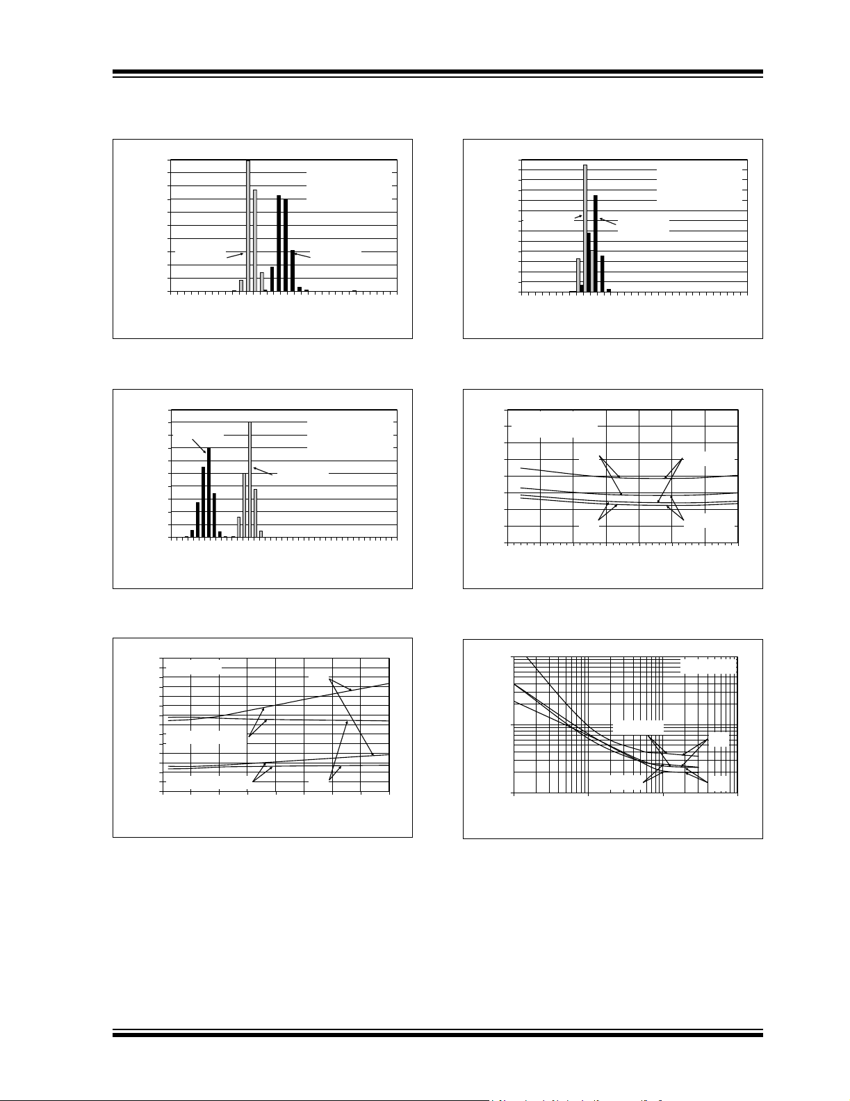
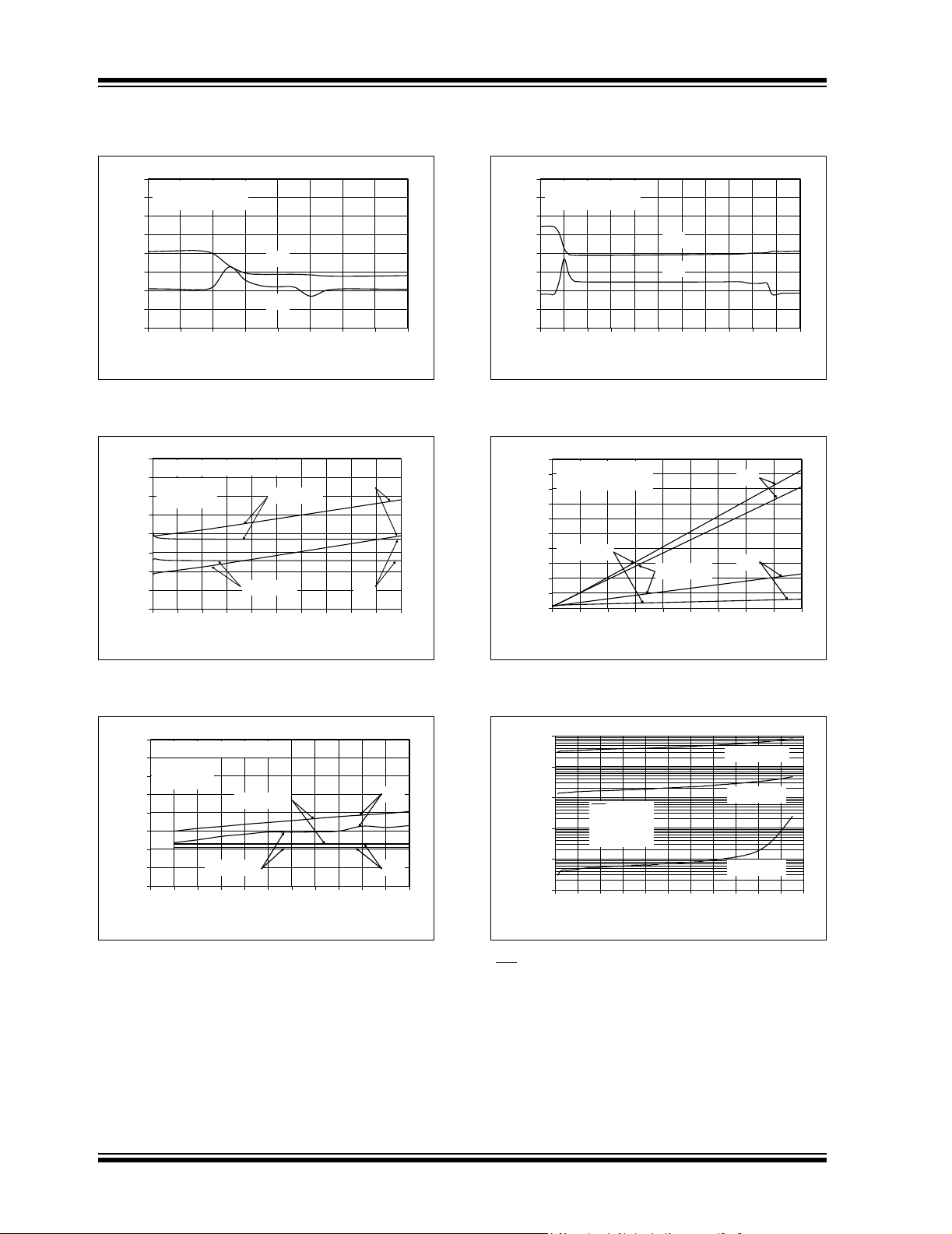
2.0 TYPICAL PERFORMANCE CURVES
Note: The graphs and tables provided following this note are a statistical summary based on a limited number of
samples and are provided for informational purposes only. The performance characteristics listed herein
are not tested or guaranteed. In some graphs or tables, the data presented may be outside the specified
operating range (e.g., outside specified power supply range) and therefore outside the warranted range.
Note: Unless otherwise indicated, VDD = +1.6V to +5.5V, VSS = GND, TA = +25°C, VIN+ = VDD/2, VIN– = GND,
R
= 2.74 kΩ to VPU=VDD, and CL = 36 pF.
PU
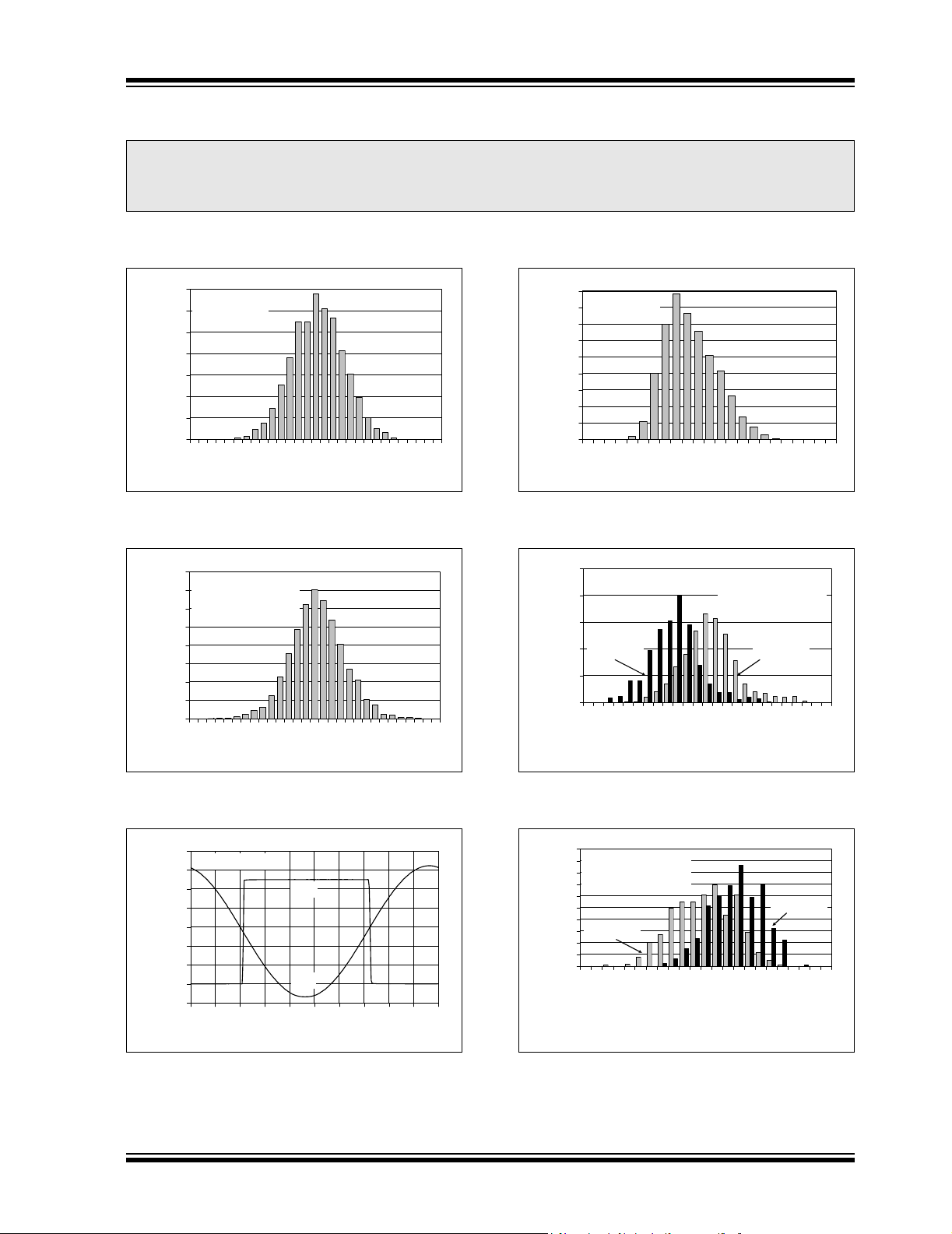
14%
1200 Samples
Percentage of Occurrences
12%
10%
8%
6%
4%
2%
0%
= V
V
CM
SS
-7-6-5-4-3-2-101234567
Input Offset Voltage (mV)
FIGURE 2-1: Input Offset Voltage at
V
CM=VSS
Percentage of Occurrences
.
16%
1200 Samples
14%
12%
10%
8%
6%
4%
2%
0%
= V
V
CM
TA = -40°C to +125°C
-14
-12
SS
-8-6-4
-10
Input Offset Voltage Drift (µV/°C)
02468
-2
101214
18%
1200 Samples
16%
V
= V
CM
SS
1.62.02.42.83.23.64.04.44.85.25.66.0
Input Hysteresis Voltage (mV)
Percentage of Occurrences
14%
12%
10%
8%
6%
4%
2%
0%
FIGURE 2-4: Input Hysteresis Voltage at
V
CM=VSS
Percentage of Occurrences
25%
20%
15%
10%
5%
0%
.
4.6
5.0
5.4
Input Hysteresis Voltage –
Linear Temp. Co.; TC
5.8
6.2
TA = -40°C to +125°C
6.6
7.0
7.4
7.8
(µV/°C)
1
596 Samples
= V
V
CM
VDD = 1.6VVDD = 5.5V
8.2
8.6
9.0
SS
9.4
FIGURE 2-2: Input Offset Voltage Drift at
V
CM=VSS
Inverting Input, Output
.
7
VDD = 5.5V
6
5
4
3
2
Voltage (V)
1
0
-1
012345678910
V
OUT
VIN–
Time (1 ms/div)
FIGURE 2-3: The MCP6546/6R/6U/7/8/9 comparators show no phase reversal.
FIGURE 2-5: Input Hysteresis Voltage
Linear Temp. Co. (TC
20%
596 Samples
18%
V
= V
CM
SS
TA = -40°C to +125°C
VDD = 1.6V
-0.060
-0.056
Quadratic Temp. Co.; TC
Percentage of Occurrences
16%
14%
12%
10%
8%
6%
4%
2%
0%
) at VCM=VSS.
1
-0.052
-0.048
-0.044
-0.040
-0.036
Input Hysteresis Voltage –
-0.032
(µV/°C2)
2
VDD = 5.5V
-0.028
-0.024
-0.020
FIGURE 2-6: Input Hysteresis Voltage
Quadratic Temp. Co. (TC
) at VCM=VSS.
2
-0.016
© 2006 Microchip Technology Inc. DS21714E-page 5
MCP6546/6R/6U/7/8/9
Note: Unless otherwise indicated, VDD= +1.6V to +5.5V, VSS= GND, TA= +25°C, VIN+=VDD/2, VIN– = GND,
RPU=2.74kΩ to VPU=VDD, and CL=36pF.
1.0
VCM = V
0.8
0.6
0.4
0.2
0.0
-0.2
-0.4
-0.6
-0.8
Input Offset Voltage (mV)
-1.0
-50 -25 0 25 50 75 100 125
SS
VDD = 1.6V
VDD = 5.5V
Ambient Temperature (°C)
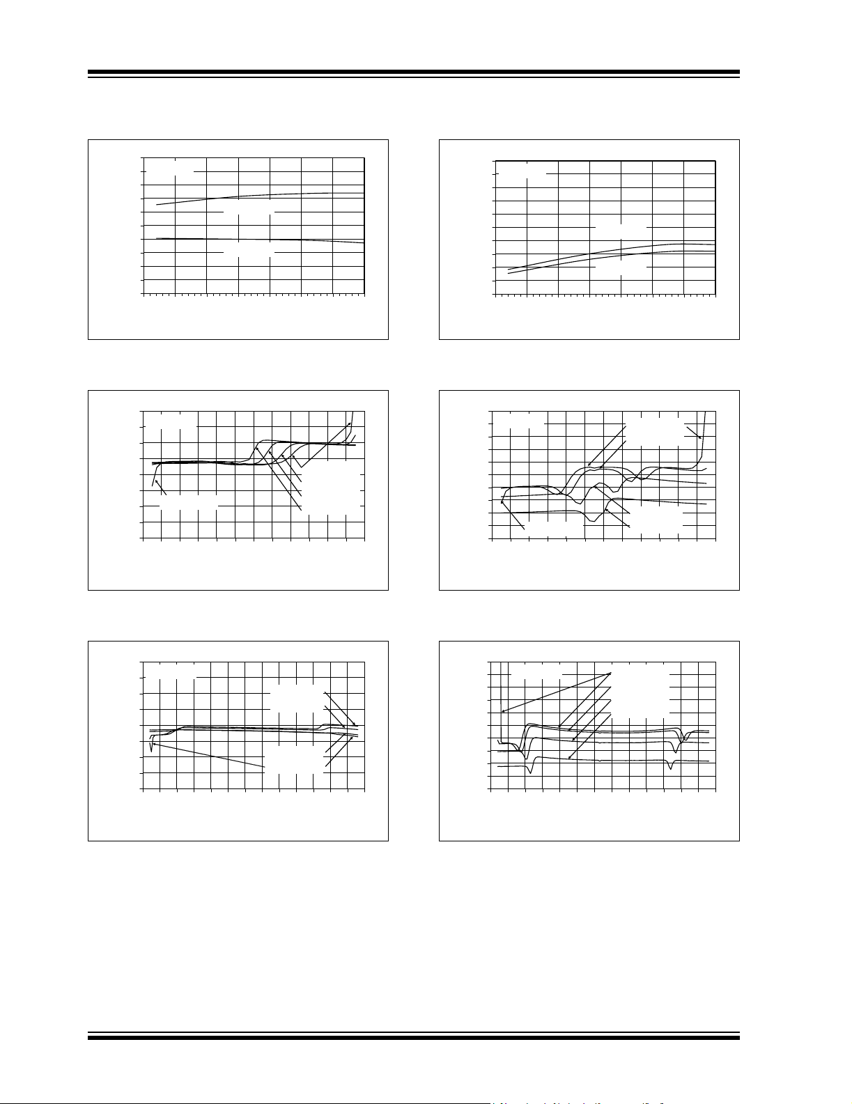
FIGURE 2-7: Input Offset Voltage vs.
Ambient Temperature at V
2.0
VDD = 1.6V
1.5
1.0
0.5
0.0
-0.5
-1.0
-1.5
Input Offset Voltage (mV)
-2.0
TA = +125°C
0.0
0.2
0.4
-0.4
-0.2
Common Mode Input Voltage (V)
0.6
CM=VSS
0.8
1.0
.
TA = +125°C
T
= +85°C
A
T
= +25°C
A
T
= -40°C
A
1.2
1.4
1.6
1.8
6.5
VCM = V
6.0
5.5
5.0
4.5
4.0
3.5
3.0
2.5
2.0
1.5
Input Hysteresis Voltage (mV)
-50-250 255075100125
SS
VDD = 1.6V
VDD = 5.5V
Ambient Temperature (°C)
FIGURE 2-10: Input Hysteresis Voltage vs.
Ambient Temperature at V
6.5
VDD = 1.6V
6.0
5.5
5.0
4.5
4.0
3.5
3.0
2.5
2.0
1.5
Input Hysteresis Voltage (mV)
2.0
TA = +125°C
0.0
-0.4
0.2
-0.2
Common Mode Input Voltage (V)
0.4
CM=VSS
0.6
0.8
.
TA = +125°C
T
= +85°C
A
TA = +25°C
T
= -40°C
A
1.0
1.2
1.4
1.6
1.8
2.0
FIGURE 2-8: Input Offset Voltage vs.
Common Mode Input Voltage at V
2.0
VDD = 5.5V
1.5
1.0
0.5
0.0
-0.5
-1.0
-1.5
Input Offset Voltage (mV)
-2.0
0.0
0.5
1.0
1.5
-0.5
Common Mode Input Voltage (V)
2.0
2.5
TA = -40°C
T
TA = +85°C
T
A
3.0
DD
= +25°C
A
= +125°C
3.5
4.0
=1.6V.
4.5
5.0
FIGURE 2-9: Input Offset Voltage vs.
Common Mode Input Voltage at V
= 5.5V.
DD
FIGURE 2-11: Input Hysteresis Voltage vs.
3.5
DD
4.0
=1.6V.
4.5
5.0
5.5
6.0
Common Mode Input Voltage at V
6.5
6.0
5.5
5.0
4.5
4.0
3.5
3.0
2.5
2.0
1.5
Input Hysteresis Voltage (mV)
5.5
6.0
VDD = 5.5V TA = +125°C
0.0
0.5
1.0
-0.5
1.5
Common Mode Input Voltage (V)
T
T
T
2.0
2.5
3.0
= +85°C
A
= +25°C
A
= -40°C
A
FIGURE 2-12: Input Hysteresis Voltage vs.
Common Mode Input Voltage at V
DD
=5.5V.
DS21714E-page 6 © 2006 Microchip Technology Inc.
MCP6546/6R/6U/7/8/9
Note: Unless otherwise indicated, VDD= +1.6V to +5.5V, VSS= GND, TA= +25°C, VIN+=VDD/2, VIN– = GND,
RPU=2.74kΩ to VPU=VDD, and CL=36pF.
10n
90
Input Referred
85
80
75
PSRR, VIN+ = VSS, VDD = 1.6V to 5.5V
70
65
CMRR, PSRR (dB)
CMRR, VIN+ = -0.3 to 5.3V, VDD = 5.0V
60
55
-50 -25 0 25 50 75 100 125
Ambient Temperature (°C)
10000
1n
1000
100p
100
(A)
10p
10
1
1p
Input Bias, Offset Currents
100f
0.1
0.00.51.01.52.02.53.03.54.04.55.05.5
IB, TA = +125°C
IB, TA = +85°C
IOS, TA = +125°C
IOS, TA = +85°C
Common Mode Input Voltage (V)
VDD = 5.5V
FIGURE 2-13: CMRR,PSRR vs. Ambient Temperature.
1000
VDD = 5.5V
V
= V
CM
100
10
(pA)
1
Input Bias, Offset Currents
0.1
55 65 75 85 95 105 115 125
DD
I
B
Ambient Temperature (°C)
| IOS |
FIGURE 2-14: Input Bias Current, Input Offset Current vs. Ambient Temperature.
0.8
IQ does not include pull-up resistor current
0.7
VDD = 1.6V
0.6
0.5
0.4
0.3
0.2
Quiescent Current
Sweep VIN+, VIN– = VDD/2
per Comparator (µA)
0.1
0.0
0.0 0.2 0.4 0.6 0.8 1.0 1.2 1.4 1.6
Common Mode Input Voltage (V)
Sweep VIN–, VIN+ = VDD/2
FIGURE 2-16: Input Bias Current, Input Offset Current vs. Common Mode Input Voltage.
0.7
0.6
0.5
0.4
0.3
0.2
Quiescent Current
per Comparator (µA)
0.1
0.0
0.00.51.01.52.02.53.03.54.04.55.05.5
TA = +125°C
T
= +85°C
A
T
= +25°C
A
T
= -40°C
A
Power Supply Voltage (V)
FIGURE 2-17: Quiescent Current vs. Power Supply Voltage.
0.8
IQ does not include pull-up resistor current
0.7
VDD = 5.5V
0.6
0.5
0.4
0.3
0.2
Quiescent Current
Sweep VIN+, VIN– = VDD/2
per Comparator (µA)
0.1
0.0
0.0 0.5 1.0 1.5 2.0 2.5 3.0 3.5 4.0 4.5 5.0 5.5
Common Mode Input Voltage (V)
Sweep VIN–, VIN+ = VDD/2
FIGURE 2-15: Quiescent Current vs.
Common Mode Input Voltage at V
DD
=1.6V.
FIGURE 2-18: Quiescent Current vs.
Common Mode Input Voltage at VDD=5.5V.
© 2006 Microchip Technology Inc. DS21714E-page 7
MCP6546/6R/6U/7/8/9
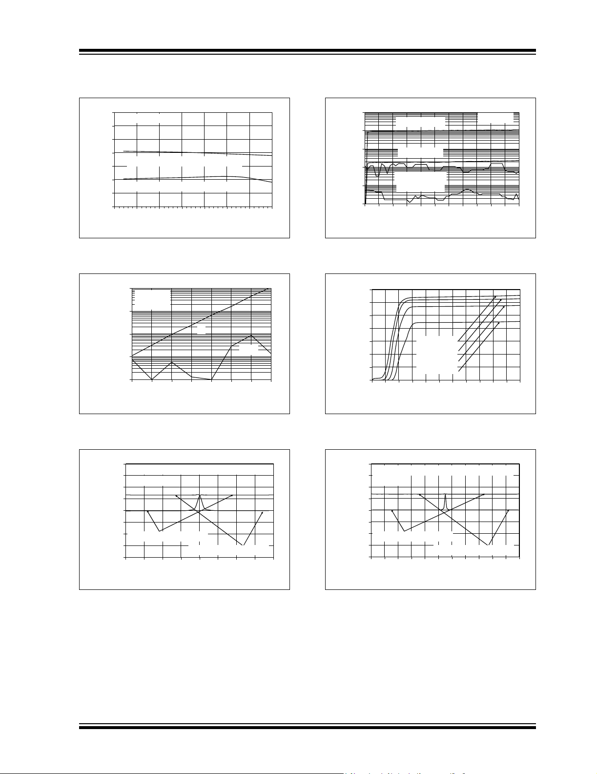
Note: Unless otherwise indicated, VDD= +1.6V to +5.5V, VSS= GND, TA= +25°C, VIN+=VDD/2, VIN– = GND,
RPU=2.74kΩ to VPU=VDD, and CL=36pF.
10
Supply Current
per Comparator (µA)
0.1
IDD spike near VPU = 1.3V
1
VDD = 1.6V
01234567891011
Pull-Up Voltage, V
VDD = 2.1V
V
= 2.6V
DD
V
= 3.6V
DD
V
= 4.6V
DD
V
= 5.6V
DD
(V)
PU
FIGURE 2-19: Supply Current vs. Pull-Up
Voltage.
10
100 mV Overdrive
= VDD/2
V
CM
does not include
I
DD
pull-up resistor current
1
Supply Current
per Comparator (µA)
0.1
0.1 1 10 100
Toggle Frequency (kHz)
VDD = 5.5V
V
= 1.6V
DD
10
1
Supply Current
per Comparator (µA)
0.1
-4-3-2-10123456789
VDD = 5.6V
= 4.6V
V
DD
V
= 3.6V
DD
= 2.6V
V
DD
Pull-up to Supply Voltage Difference,
V
VDD = 1.6V
= 2.1V
V
DD
– VDD (V)
PU
VPU = 1.6V to 10.5V
FIGURE 2-22: Supply Current vs. Pull-Up
to Supply Voltage Difference.
35
30
25
20
15
10
Magnitude (mA)
5
Output Short Circuit Current
0
0.0 0.5 1.0 1.5 2.0 2.5 3.0 3.5 4.0 4.5 5.0 5.5
TA = -40°C
= +25°C
T
A
= +85°C
T
A
= +125°C
T
A
Power Supply Voltage (V)
FIGURE 2-20: Supply Current vs. Toggle Frequency.
0.8
VDD = 1.6V
0.7
0.6
0.5
0.4
0.3
0.2
0.1
Output Voltage Headroom (V)
0.0
0.0 0.2 0.4 0.6 0.8 1.0 1.2 1.4 1.6
VOL–VSS:
T
= +125°C
A
T
= +85°C
A
T
= +25°C
A
T
= -40°C
A
Output Current (mA)
FIGURE 2-21: Output Voltage Headroom
vs. Output Current at V
DD
=1.6V.
FIGURE 2-23: Output Short Circuit Current Magnitude vs. Power Supply Voltage.
1.0
VDD = 5.5V
0.9
0.8
0.7
0.6
0.5
0.4
0.3
0.2
0.1
Output Voltage Headroom (V)
0.0
0 5 10 15 20 25
Output Current (mA)
VOL – VSS:
TA = +125°C
T
= +85°C
A
T
= +25°C
A
T
= -40°C
A
FIGURE 2-24: Output Voltage Headroom
vs. Output Current at VDD=5.5V.
DS21714E-page 8 © 2006 Microchip Technology Inc.
MCP6546/6R/6U/7/8/9
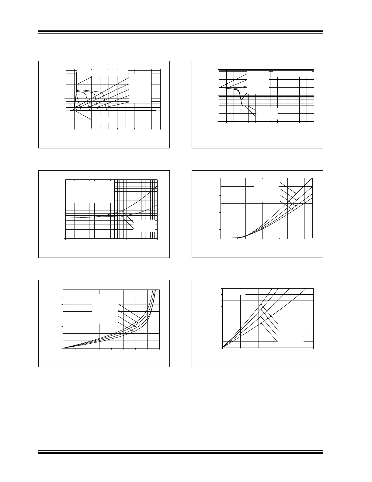
Note: Unless otherwise indicated, VDD= +1.6V to +5.5V, VSS= GND, TA= +25°C, VIN+=VDD/2, VIN– = GND,
RPU=2.74kΩ to VPU=VDD, and CL=36pF.
50%
45%
40%
35%
30%
25%
20%
15%
10%
5%
Percentage of Occurrences
0%
012345678
High-to-Low Propagation Delay (µs)
408 Samples
100 mV Overdrive
= VDD/2
V
CM
VDD = 5.5VVDD = 1.6V
FIGURE 2-25: High-to-Low Propagation Delay.
50%
45%
VDD = 5.5V
40%
35%
30%
25%
20%
15%
10%
5%
Percentage of Occurrences
0%
-2.0
-1.6
-1.2
Propagation Delay Skew (µs)
-0.8
VDD = 1.6V
0.0
-0.4
408 Samples
100 mV Overdrive
V
= VDD/2
CM
0.4
0.8
1.2
1.6
65%
60%
55%
50%
45%
40%
VDD = 1.6V
35%
30%
25%
20%
15%
10%
5%
Percentage of Occurrences
0%
012345678
Low-to-High Propagation Delay (µs)
VDD = 5.5V
408 Samples
100 mV Overdrive
= VDD/2
V
CM
FIGURE 2-28: Low-to-High Propagation Delay.
8
100 mV Overdrive
7
= VDD/2
V
CM
6
5
4
3
2
1
Propagation Delay (µs)
2.0
0
-50 -25 0 25 50 75 100 125
t
PHL
t
PLH
Ambient Temperature (°C)
VDD = 5.5V
VDD = 1.6V
FIGURE 2-26: Propagation Delay Skew.
14
VCM = VDD/2
13
12
11
10
9
8
7
6
10 mV Overdrive
5
4
3
2
Propagation Delay (µs)
1
100 mV Overdrive
0
1.52.02.53.03.54.04.55.05.5
Power Supply Voltage (V)
t
PHL
t
PLH
FIGURE 2-27: Propagation Delay vs. Power Supply Voltage.
FIGURE 2-29: Propagation Delay vs. Ambient Temperature.
100
10
Propagation Delay (µs)
1
1 10 100 1000
VDD = 5.5V
VDD = 1.6V
Input Overdrive (mV)
VCM = VDD/2
t
PHL
t
PLH
FIGURE 2-30: Propagation Delay vs. Input Overdrive.
© 2006 Microchip Technology Inc. DS21714E-page 9
MCP6546/6R/6U/7/8/9
Note: Unless otherwise indicated, VDD= +1.6V to +5.5V, VSS= GND, TA= +25°C, VIN+=VDD/2, VIN– = GND,
RPU=2.74kΩ to VPU=VDD, and CL=36pF.
8
VDD = 1.6V
7
100 mV Overdrive
6
5
4
3
2
1
Propagation Delay (µs)
0
0.0 0.2 0.4 0.6 0.8 1.0 1.2 1.4 1.6
Common Mode Input Voltage (V)
t
PHL
t
PLH
FIGURE 2-31: Propagation Delay vs.
Common Mode Input Voltage at V
8
VIN– = 100 mV Overdrive
7
VCM = VDD/2
6
+ = V
V
IN
5
4
3
2
Propagation Delay (µs)
1
0
0 102030405060708090100
CM
Pull-up Resistor, R
VDD = 5.5V
VDD = 1.6V
PU
(k:)
DD
=1.6V.
t
PLH
t
PHL
8
VDD = 5.5V
7
100 mV Overdrive
6
5
4
3
2
1
Propagation Delay (µs)
0
0.00.51.01.52.02.53.03.54.04.55.05.5
Common Mode Input Voltage (V)
t
PHL
t
PLH
FIGURE 2-34: Propagation Delay vs.
Common Mode Input Voltage at VDD=5.5V.
200
100 mV Overdrive
180
160
140
120
100
Propagation Delay (µs)
= VDD/2
V
CM
80
VDD = 5.5V
60
40
20
0
0 102030405060708090
VDD = 1.6V
Load Capacitance (nF)
t
PLH
t
PHL
FIGURE 2-32: Propagation Delay vs.
Pull-up Resistor.
8
VIN– = 100 mV Overdrive
7
VCM = VDD/2
6
V
+ = V
IN
5
4
3
2
1
Propagation Delay (µs)
0
CM
VDD = 5.5V
VDD = 1.6V t
01234567891011
Pull-up Voltage (V)
FIGURE 2-33: Propagation Delay vs.
Pull-up Voltage.
FIGURE 2-35: Propagation Delay vs. Load Capacitance.
10n
1.E+04
1n
1.E+03
t
PHL
PLH
100p
1.E+02
1.E+01
10p
1.E+00
Output Leakage Current (A)
1.E-01
100f
1p
CS = V
DD
VIN+ = VDD/2
V
– = V
IN
SS
01234567891011
Output Voltage (V)
TA = +125°C
TA = +85°C
TA = +25°C
FIGURE 2-36: Output Leakage Current
=VDD) vs. Output Voltage (MCP6548 only).
(CS
DS21714E-page 10 © 2006 Microchip Technology Inc.

MCP6546/6R/6U/7/8/9
r
f
r
f
Note: Unless otherwise indicated, VDD= +1.6V to +5.5V, VSS= GND, TA= +25°C, VIN+=VDD/2, VIN– = GND,
RPU=2.74kΩ to VPU=VDD, and CL=36pF.
1m
1.E-03
1m
Comparator
100µ
Turns On
10µ
1µ
100n
10n
1n
100p
VDD = 1.6V
10p
0.0 0.2 0.4 0.6 0.8 1.0 1.2 1.4 1.6
CS
High-to-Low
Chip Select (CS) Voltage (V)
Supply Current
1.E-04
1.E-05
1.E-06
1.E-07
1.E-08
1.E-09
per Comparator (A)
1.E-10
1.E-11
Comparato
Shuts Of
CS Hysteresis
CS
Low-to-High
1.E-03
Comparator
100µ
1.E-04
Turns On
10µ
1.E-05
1µ
1.E-06
100n
1.E-07
10n
1.E-08
Supply Current
1.E-09
per Comparator (A)
100p
1.E-10
10p
1.E-11
CS
1n
Low-to-High
0.00.51.01.52.02.53.03.54.04.55.05.5
Chip Select (CS) Voltage (V)
CS
Hysteresis
High-to-Low
VDD = 5.5V
Comparato
Shuts Of
CS
FIGURE 2-37: Supply Current (shoot
through current) vs. Chip Select (CS
V
= 1.6V (MCP6548 only).
DD
30
25
20
VDD = 1.6V
15
10
5
0
Supply Current (µA)
Charging output
capacitance
01234567891011121314
Time (1 ms/div)
V
OUT
CS
Start-up
I
DD
) Voltage at
1.6
0.0
-1.6
-3.2
Output Voltage,
-4.9
-6.5
-8.1
FIGURE 2-38: Supply Current (charging
current) vs. Chip Select (CS
) pulse at VDD=1.6V
(MCP6548 only).
6.0
5.5
5.0
4.5
4.0
3.5
3.0
(V)
2.5
2.0
1.5
1.0
0.5
0.0
Chip Select, Output Voltage
-0.5
012345678910
VDD = 5.5V
V
OUT
CS
Time (ms)
FIGURE 2-40: Supply Current (shoot
through current) vs. Chip Select (CS
V
= 5.5V (MCP6548 only).
DD
200
180
V
OUT
160
140
120
100
80
Chip Select Voltage (V),
60
40
20
Supply Current
0
per Comparator (µA)
0.0 0.5 1.0 1.5 2.0 2.5 3.0 3.5
CS
Start-up I
VDD = 5.5V
Charging output
capacitance
Time (0.5 ms/div)
) Voltage at
6
3
0
-3
-6
DD
-9
-12
-15
-18
-21
-24
Output Voltage,
Chip Select Voltage (V)
FIGURE 2-41: Supply Current (charging
current) vs. Chip Select (CS
) pulse at VDD=5.5V
(MCP6548 only).
1.E-02
10m
1.E-03
1m
1.E-04
100µ
1.E-05
10µ
1.E-06
1µ
100n
1.E-07
10n
1.E-08
1n
1.E-09
100p
1.E-10
10p
1.E-11
Input Current Magnitude (A)
1p
1.E-12
-1.0 -0.9 -0.8 -0.7 -0.6 -0.5 -0.4 -0.3 -0.2 -0.1 0.0
+125°C
+85°C
+25°C
-40°C
Input Voltage (V)
FIGURE 2-39: Chip Select (CS
Response (MCP6548 only).
) Step
FIGURE 2-42: Input Bias Current vs. Input Voltage.
© 2006 Microchip Technology Inc. DS21714E-page 11

MCP6546/6R/6U/7/8/9
3.0 PIN DESCRIPTIONS
Descriptions of the pins are listed in Table 3-1.
TABLE 3-1: PIN FUNCTION TABLE
MCP6546
(PDIP,
SOIC,
MSOP)
————5—5V
————6—6V
— — — — 7 — 7 OUTB Digital Output (comparator B)
— — — — — — 8 OUTC Digital Output (comparator C)
——————9V
——————10V
——————12V
——————13V
— — — — — — 14 OUTD Digital Output (comparator D)
—————8—CS
1, 5, 8 — — — — 1, 5 — NC No Internal Connection
MCP6546
(SOT-23-5,
SC-70-5)
MCP6546R
MCP6546U
MCP6547
MCP6548
Symbol Description
MCP6549
6 1 1 4 1 6 1 OUT, OUTA Digital Output (comparator A)
2441222V
3333333V
IN
IN
–, V
– Inverting Input (comparator A)
INA
+, V
+ Non-inverting Input (comparator A)
INA
7525874VDDPositive Power Supply
+ Non-inverting Input (comparator B)
INB
– Inverting Input (comparator B)
INB
– Inverting Input (comparator C)
INC
+ Non-inverting Input (comparator C)
INC
42524411V
SS
IND
IND
Negative Power Supply
+ Non-inverting Input (comparator D)
– Inverting Input (comparator D)
Chip Select
3.1 Analog Inputs
The comparator non-inverting and inverting inputs are
high-impedance CMOS inputs with low bias currents.
3.2 CS Digital Input
This is a CMOS, Schmitt-triggered input that places the
part into a low power mode of operation.
3.3 Digital Outputs
The comparator outputs are CMOS, open-drain digital
outputs. They are designed to make level shifting and
wired-OR easy to implement.
3.4 Power Supply (VSS and VDD)
The positive power supply pin (VDD) is 1.6V to 5.5V
higher than the negative power supply pin (V
normal operation, the other pins are at voltages
between VSS and VDD, except the output pins which
can be as high as 10V above V
SS
.
Typically, these parts are used in a single (positive)
supply configuration. In this case, V
is connected to
SS
ground and VDD is connected to the supply. VDD will
need a local bypass capacitor (typically 0.01 µF to
0.1 µF) within 2 mm of the V
pin. These can share a
DD
bulk capacitor with nearby analog parts (within
100 mm), but it is not required.
SS
). For
DS21714E-page 12 © 2006 Microchip Technology Inc.

4.0 APPLICATIONS INFORMATION
The MCP6546/7/8/9 family of push-pull output
comparators are fabricated on Microchip’s state-of-theart CMOS process. They are suitable for a wide range
of applications requiring very low power consumption.
4.1 Comparator Inputs
4.1.1 PHASE REVERSAL
The MCP6546/6R/6U/7/8/9 comparator family uses
CMOS transistors at the input. They are designed to
prevent phase inversion when the input pins exceed
the supply voltages. Figure 2-3 shows an input voltage
exceeding both supplies with no resulting phase
inversion.
4.1.2 INPUT VOLTAGE AND CURRENT
LIMITS
The ESD protection on the inputs can be depicted as
shown in Figure 4-1. This structure was chosen to protect the input transistors, and to minimize input bias
current (IB). The input ESD diodes clamp the inputs
when they try to go more than one diode drop below
. They also clamp any voltages that go too far
V
SS
above V
allow normal operation, and low enough to bypass ESD
events within the specified limits.
FIGURE 4-1: Simplified Analog Input ESD Structures.
In order to prevent damage and/or improper operation
of these amplifiers, the circuits they are in must limit the
currents (and voltages) at the V
Absolute Maximum Ratings † at the beginning of
Section 1.0 “Electrical Characteristics”). Figure 4-3
shows the recommended approach to protecting these
inputs. The internal ESD diodes prevent the input pins
(V
IN
the resistors R1 and R2 limit the possible current drawn
out of the input pin. Diodes D
pin (V
When implemented as shown, resistors R1 and R2 also
limit the current through D
; their breakdown voltage is high enough to
DD
Bond
V
DD
Pad
VIN+
V
SS
Bond
Pad
Bond
Pad
Input
Stage
Bond
+ and VIN– pins (see
IN
Pad
VIN–
+ and VIN–) from going too far below ground, and
and D2 prevent the input
+ and VIN–) from going too far above VDD.
IN
1
and D2.
1
MCP6546/6R/6U/7/8/9
V
DD
D
1
V
1
R
1
D
2
V
2
R
2
VSS– (minimum expected V1)
R
≥
1
VSS– (minimum expected V2)
R
≥
2
FIGURE 4-2: Protecting the Analog Inputs.
It is also possible to connect the diodes to the left of the
resistors R1 and R2. In this case, the currents through
the diodes D1 and D2 need to be limited by some other
mechanism. The resistor then serves as in-rush current
limiter; the DC current into the input pins (V
VIN–) should be very small.
A significant amount of current can flow out of the
inputs when the common mode voltage (V
ground (VSS); see Figure 2-42. Applications that are
high impedance may need to limit the useable voltage
range.
4.1.3 NORMAL OPERATION
The input stage of this family of devices uses two
differential input stages in parallel: one operates at low
input voltages and the other at high input voltages.
With this topology, the input voltage is 0.3V above V
and 0.3V below VSS. The input offset voltage is
measured at both V
proper operation.
The MCP6546/6R/6U/7/8/9 family has internally-set
hysteresis that is small enough to maintain input offset
accuracy (<7 mV), and large enough to eliminate
output chattering caused by the comparator’s own
input noise voltage (200 µV
this capability.
SS
+
MCP6G0X
–
R
3
2mA
2mA
- 0.3V and V
). Figure 4-3 illustrates
P-P
V
OUT
) is below
CM
+ 0.3V to ensure
DD
+ and
IN
DD
© 2006 Microchip Technology Inc. DS21714E-page 13
MCP6546/6R/6U/7/8/9
8
VDD = 5.0V
7
6
5
V
4
3
2
1
0
Output Voltage (V)
-1
-2
-3
OUT
Time (100 ms/div)
VIN–
Hysteresis
FIGURE 4-3: The MCP6546/7/8/9
comparators’ internal hysteresis eliminates
output chatter caused by input noise voltage.
4.2 Open-Drain Output
25
20
15
10
5
0
-5
-10
-15
-20
-25
-30
Input Voltage (10 mV/div)
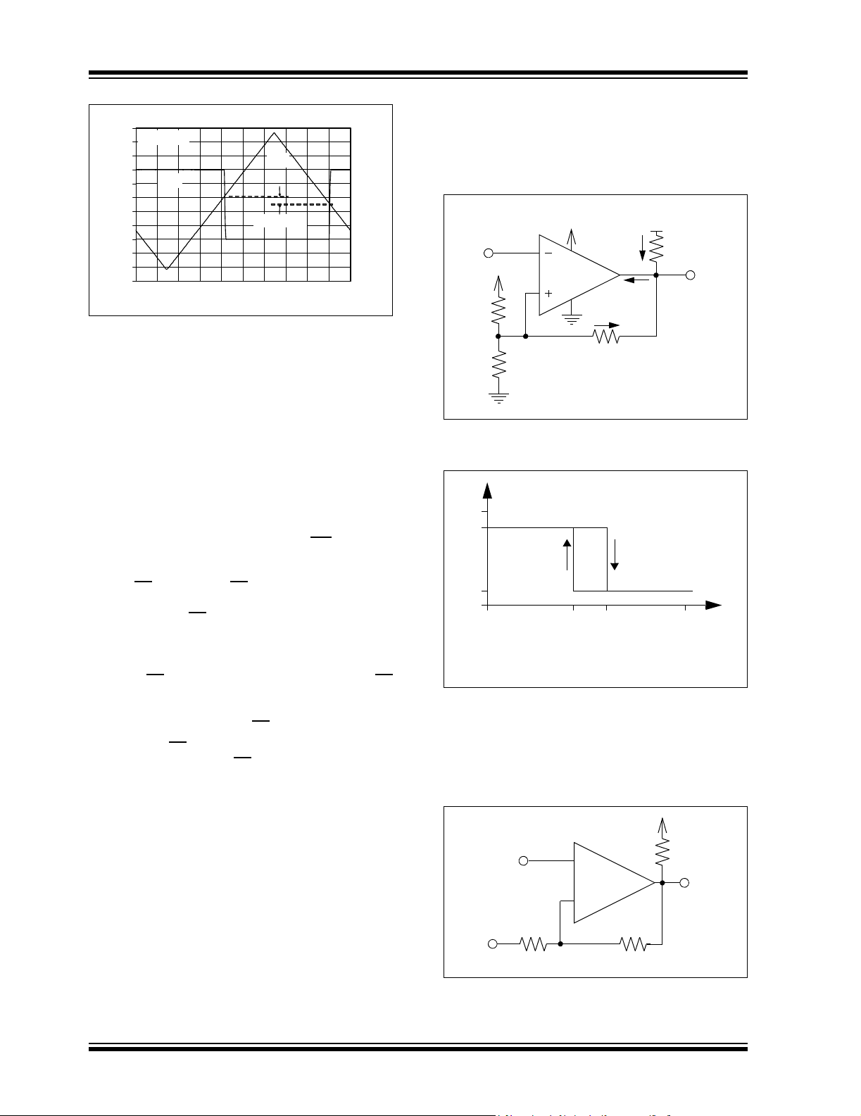
4.4.1 INVERTING CIRCUIT
Figure 4-4 shows an inverting circuit for a single-supply
application using three resistors, besides the pull-up
resistor. The resulting hysteresis diagram is shown in
Figure 4-5.
V
DD
V
IN
V
DD
R
2
R
3
MCP654X
I
RF
R
V
PU
I
PU
F
I
OL
R
PU
V
OUT
The open-drain output is designed to make levelshifting and wired-OR logic easy to implement. The
output can go as high as 10V for 9V battery-powered
applications. The output stage minimizes switching current (shoot-through current from supply-to-supply)
when the output changes state. See Figures 2-15, 2-18
and 2-37 through 2-41, for more information.
4.3 MCP6548 Chip Select (CS)
The MCP6548 is a single comparator with a Chip
Select (CS) pin. When CS is pulled high, the total
current consumption drops to 20 pA (typ.). 1 pA (typ.)
flows through the CS
pin, 1 pA (typ.) flows through the
output pin and 18 pA (typ.) flows through the VDD pin,
as shown in Figure 1-1. When this happens, the
comparator output is put into a high-impedance state.
By pulling CS
low, the comparator is enabled. If the CS
pin is left floating, the comparator will not operate
properly. Figure 1-1 shows the output voltage and
supply current response to a CS
The internal CS
circuitry is designed to minimize
pulse.
glitches when cycling the CS pin. This helps conserve
power, which is especially important in battery-powered
applications.
4.4 Externally Set Hysteresis
Greater flexibility in selecting hysteresis, or input trip
points, is achieved by using external resistors.
Input offset voltage (V
(input-referred) low-high and high-low trip points. Input
hysteresis voltage (V
the same trip points. Hysteresis reduces output
chattering when one input is slowly moving past the
other, thus reducing dynamic supply current. It also
helps in systems where it is best not to cycle between
states too frequently (e.g., air conditioner thermostatic
control).
) is the center (average) of the
OS
) is the difference between
HYST
FIGURE 4-4: Inverting circuit with hysteresis.
V
OUT
V
PU
V
OH
High-to-LowLow-to-High
V
OL
V
SS
V
SS
V
= trip voltage from low to high
TLH
= trip voltage from high to low
V
THL
V
TLHVTHL
V
IN
V
DD
FIGURE 4-5: Hysteresis diagram for the inverting circuit.
In order to determine the trip voltages (V
for the circuit shown in Figure 4-4, R
simplified to the Thevenin equivalent circuit with
respect to VDD, as shown in Figure 4-6.
-
MCP654X
+
V
23
R
23
R
F
and V
THL
and R3 can be
2
V
R
PU
PU
V
TLH
OUT
FIGURE 4-6: Thevenin Equivalent Circuit.
)
DS21714E-page 14 © 2006 Microchip Technology Inc.

MCP6546/6R/6U/7/8/9
EQUATION 4-1:
R2R
------------------
R2R3+
R
3
3
VDD×=
=
R
23
------------------
V
23
R2R3+
Using this simplified circuit, the trip voltage can be
calculated using the following equation:
EQUATION 4-2:
R
V
THL
V
V
TLH
THL
⎛⎞
V
⎜⎟
PU
⎝⎠
V
TLH
= trip voltage from low to high
= trip voltage from high to low
23
---------------------------------------R23RFR
++
V
OL
PU
R
⎛⎞
23
---------------------- -
⎜⎟
R23RF+
⎝⎠
+=
V
+=
V
Figure 2-21 and Figure 2-24 can be used to determine
typical values for V
. This voltage is dependent on the
OL
output current IOL as shown in Figure 4-4. This current
can be determined using the equation below:
RFRPU+
⎛⎞
---------------------------------------
23
⎝⎠
++
R
23RFRPU
R
F
⎛⎞
--------------------- -
23
⎝⎠
R23RF+
EQUATION 4-3:
I
OLIPUIRF
VPUVOL–
⎛⎞
I
--------------------------
OL
⎝⎠
R
VOH can be calculated using the equation below:
PU
+=
V
–
23VOL
⎛⎞
------------------------
+=
⎝⎠
R
+
23RF
4.6 Capacitive Loads
Reasonable capacitive loads (e.g., logic gates) have
little impact on propagation delay (see Figure 2-27).
The supply current increases with increasing toggle
frequency (Figure 2-30), especially with higher
capacitive loads.
4.7 Battery Life
In order to maximize battery life in portable
applications, use large resistors and small capacitive
loads. Avoid toggling the output more than necessary.
Do not use Chip Select (CS
) too frequently in order to
conserve power. Capacitive loads will draw additional
power at start-up.
4.8 PCB Surface Leakage
In applications where low input bias current is critical,
PCB (Printed Circuit Board) surface leakage effects
need to be considered. Surface leakage is caused by
humidity, dust or other contamination on the board.
Under low-humidity conditions, a typical resistance
between nearby traces is 10
would cause 5 pA of current to flow. This is greater
than the MCP6546/6R/6U/7/8/9 family’s bias current at
25°C (1 pA, typ.).
The easiest way to reduce surface leakage is to use a
guard ring around sensitive pins (or traces). The guard
ring is biased at the same voltage as the sensitive pin.
An example of this type of layout is shown in
Figure 4-7.
VIN-V
12
Ω. A 5V difference
+
IN
V
SS
EQUATION 4-4:
R
+
23RF
⎛⎞
--------------------------------------
V
VPUV23–()
OH
As explained in Section 4.1 “Comparator Inputs”, it
is important to keep the non-inverting input below
+0.3V when VPU > VDD.
V
DD
4.5 Supply Bypass
With this family of comparators, the power supply pin
for single supply) should have a local bypass
(V
DD
capacitor (i.e., 0.01 µF to 0.1 µF) within 2 mm for good
edge rate performance.
© 2006 Microchip Technology Inc. DS21714E-page 15
×=
⎝⎠
R
++
23RFRPU
Guard Ring
FIGURE 4-7: Example Guard Ring Layout for Inverting Circuit.
1. Inverting Configuration (Figures 4-4 and 4-7):
a. Connect the guard ring to the non-inverting
input pin (V
to the same reference voltage as the
comparator (e.g., VDD/2 or ground).
b. Connect the inverting pin (V
pad without touching the guard ring.
+). This biases the guard ring
IN
–) to the input
IN

MCP6546/6R/6U/7/8/9
4.9 Unused Comparators
An unused amplifier in a quad package (MCP6549)
should be configured as shown in Figure 4-8. This
circuit prevents the output from toggling and causing
crosstalk. It uses the minimum number of components
and draws minimal current (see Figure 2-15 and
Figure 2-18).
¼ MCP6549
V
DD
–
+
FIGURE 4-8: Unused Comparators.
4.10 Typical Applications
4.10.1 PRECISE COMPARATOR
Some applications require higher DC precision. An
easy way to solve this problem is to use an amplifier
(such as the MCP6041) to gain-up the input signal
before it reaches the comparator. Figure 4-9 shows an
example of this approach.
V
DD
V
REF
MCP6041
V
V
V
IN
R
1
R
2
V
REF
MCP6546
FIGURE 4-9: Precise Inverting Comparator.
4.10.2 WINDOWED COMPARATOR
Figure 4-10 shows one approach to designing a
windowed comparator. The wired-OR connection
produces a high output (logic 1) when the input voltage
is between V
and VRT (where VRT > VRB).
RB
DD
PU
R
PU
V
OUT
V
1/2
V
RT
V
IN
V
RB
MCP6547
1/2
PU
R
PU
V
OUT
MCP6547
FIGURE 4-10: Windowed Comparator.
DS21714E-page 16 © 2006 Microchip Technology Inc.

5.0 PACKAGING INFORMATION
5.1 Package Marking Information
5-Lead SC-70 (MCP6546)
MCP6546/6R/6U/7/8/9
Example: (I-temp)
I-Temp
Code
2005 are marked “ACN”
available at this release of
the data sheet.
XXNN (Front)
YWW (Back)
Device
MCP6546 ACNN Note 2
Note 1: I-Temp parts prior to March
2: SC-70-5 E-Temp parts not
5-Lead SOT-23 (MCP6546, MCP6546R, MCP6546U)
Device
XXNN AC25
MCP6546 ACNN GWNN
MCP6546R AHNN GXNN
MCP6546U — AWNN
Note: Applies to 5-Lead SOT-23
I-Temp
Code
8-Lead PDIP (300 mil)
XXXXXXXX
XXXXXNNN
YYWW
8-Lead SOIC (150 mil)
E-Temp
Code
E-Temp
Code
MCP6546
I/P256
0636
AC25(Front)
636 (Back)
Example: (I-temp)
Example:
OR
Example:
MCP6546
3
e
I/P^^256
0636
XXXXXXXX
XXXXYYWW
NNN
8-Lead MSOP
XXXXXX
YWWNNN
MCP6546
I/SN0636
256
OR
Example:
MCP6546I
3
e
SN^^0636
256
6546I
636256
Legend: XX...X Customer-specific information
Y Year code (last digit of calendar year)
YY Year code (last 2 digits of calendar year)
WW Week code (week of January 1 is week ‘01’)
NNN Alphanumeric traceability code
Pb-free JEDEC designator for Matte Tin (Sn)
3
e
* This package is Pb-free. The Pb-free JEDEC designator ( )
3
e
can be found on the outer packaging for this package.
Note: In the event the full Microchip part number cannot be marked on one line, it will
be carried over to the next line, thus limiting the number of available
characters for customer-specific information.
© 2006 Microchip Technology Inc. DS21714E-page 17

MCP6546/6R/6U/7/8/9
Package Marking Information (Continued)
14-Lead PDIP (300 mil) (MCP6549) Example:
XXXXXXXXXXXXXX
XXXXXXXXXXXXXX
YYWWNNN
14-Lead SOIC (150 mil) (MCP6549)
XXXXXXXXXX
XXXXXXXXXX
YYWWNNN
OR
OR
MCP6549-I/P
XXXXXXXXXXXXXX
MCP6549E/P
Example:
0636256
e
0636256
MCP6549
I/P^^
3
e
0636256
MCP6549ISL
XXXXXXXXXX
0636256
3
14-Lead TSSOP (MCP6549)
XXXXXXXX
YYWW
NNN
OR
Example:
MCP6549I
0636
256
MCP6549
e
E/SL^^
0636256
3
DS21714E-page 18 © 2006 Microchip Technology Inc.
MCP6546/6R/6U/7/8/9
5-Lead Plastic Package (LT) (SC-70)
Note: For the most current package drawings, please see the Microchip Packaging Specification located at
http://www.microchip.com/packaging
E
E1
D
p
n
Q1
c
Number of Pins
Pitch
Top of Molded Pkg to
Lead Shoulder
Lead Thickness
*
Controlling Parameter
Notes:
Dimensions D and E1 do not include mold flash or protrusions. Mold flash or protrusions shall not exceed .005" (0.127mm) per side.
BSC: Basic Dimension. Theoretically exact value shown without tolerances.
See ASME Y14.5M
JEITA (EIAJ) Standard: SC-70
Drawing No. C04-061
n
p
Q1
c
B
1
A2 A
A1
L
INCHESUnits
.004 .016 0.10
MILLIMETERS
55
0.65 (BSC).026 (BSC)
Revised 07-19-05
*
MAXNOMMINMAXNOMMINDimension Limits
1.100.80.043.031AOverall Height
1.000.80.039.031A2Molded Package Thickness
0.100.00.004.000A1Standoff
2.401.80.094.071EOverall Width
1.351.15.053.045E1Molded Package Width
2.201.80.087.071DOverall Length
0.300.10.012.004LFoot Length
0.40
0.180.10.007.004
0.300.15.012.006BLead Width
© 2006 Microchip Technology Inc. DS21714E-page 19

MCP6546/6R/6U/7/8/9
5-Lead Plastic Small Outline Transistor (OT) (SOT23)
Note: For the most current package drawings, please see the Microchip Packaging Specification located at
http://www.microchip.com/packaging
E
E1
B
n
c
β
Number of Pins
Pitch
Outside lead pitch
Foot Angle
Lead Thickness
Mold Draft Angle Top
Mold Draft Angle Bottom
*
Controlling Parameter
Notes:
Dimensions D and E1 do not include mold flash or protrusions. Mold flash or protrusions shall not exceed .005" (0.127mm) per side.
BSC: Basic Dimension. Theoretically exact value shown without tolerances.
See ASME Y14.5M
JEITA (formerly EIAJ) equivalent: SC-74A
Drawing No. C04-120
L
Units
n
p
p1
φ
c
α
β
p1
D
1
α
A1
A
*
MILLIMETERSINCHES
0.95 BSC.038 BSC
1.90 BSC.075 BSC
Revised 09-12-05
A2
MAXNOMMINMAXNOMMINDimension Limits
66
1.451.180.90.057.046.035AOverall Height
1.301.100.90.051.043.035A2Molded Package Thickness
0.150.080.00.006.003.000A1Standoff
3.002.802.60.118.110.102EOverall Width
1.751.631.50.069.064.059E1Molded Package Width
3.102.952.80.122.116.110DOverall Length
0.550.450.35.022.018.014LFoot Length
10501050
0.200.150.09.008.006.004
0.500.430.35.020.017.014BLead Width
10501050
10501050
φ
DS21714E-page 20 © 2006 Microchip Technology Inc.
MCP6546/6R/6U/7/8/9
8-Lead Plastic Dual In-line (P) – 300 mil Body (PDIP)
Note: For the most current package drawings, please see the Microchip Packaging Specification located at
http://www.microchip.com/packaging
E1
D
2
n
E
β
eB
Dimension Limits MIN NOM MAX MIN NOM MAX
Number of Pins
Pitch
Top to Seating Plane A .140 .155 .170 3.56 3.94 4.32
Molded Package Thickness A2 .115 .130 .145 2.92 3.30 3.68
Base to Seating Plane
Shoulder to Shoulder Width E .300 .313 .325 7.62 7.94 8.26
Molded Package Width E1 .240 .250 .260 6.10 6.35 6.60
Overall Length D .360 .373 .385 9.14 9.46 9.78
Tip to Seating Plane L .125 .130 .135 3.18 3.30 3.43
Lead Thickness
Upper Lead Width B1 .045 .058 .070 1.14 1.46 1.78
Lower Lead Width B .014 .018 .022 0.36 0.46 0.56
Overall Row Spacing §
Mold Draft Angle Top
Mold Draft Angle Bottom
* Controlling Parameter
§ Significant Characteristic
Notes:
Dimensions D and E1 do not include mold flash or protrusions. Mold flash or protrusions shall not exceed .010” (0.254mm) per side.
JEDEC Equivalent: MS-001
Drawing No. C04-018
1
α
A
c
Units INCHES* MILLIMETERS
n
p
A1
c
eB
α
β
.015 0.38
.008 .012 .015 0.20 0.29 0.38
.310 .370 .430 7.87 9.40 10.92
A1
B1
B
88
.100 2.54
51015 51015
51015 51015
A2
L
p
© 2006 Microchip Technology Inc. DS21714E-page 21

MCP6546/6R/6U/7/8/9
8-Lead Plastic Small Outline (SN) – Narrow, 150 mil (SOIC)
Note: For the most current package drawings, please see the Microchip Packaging Specification located at
http://www.microchip.com/packaging
E
E1
p
D
2
B
Number of Pins
Pitch
Standoff §
Foot Angle
Lead Thickness
Mold Draft Angle Top
Mold Draft Angle Bottom
* Controlling Parameter
§ Significant Characteristic
Notes:
Dimensions D and E1 do not include mold flash or protrusions. Mold flash or protrusions shall not exceed .010” (0.254mm) per side.
JEDEC Equivalent: MS-012
Drawing No. C04-057
n
45°
c
β
n
p
A1
φ
c
α
β
1
h
A
φ
L
048048
A1
MILLIMETERSINCHES*Units
.050
α
A2
MAXNOMMINMAXNOMMINDimension Limits
88
1.27
1.751.551.35.069.061.053AOverall Height
1.551.421.32.061.056.052A2Molded Package Thickness
0.250.180.10.010.007.004
6.206.025.79.244.237.228EOverall Width
3.993.913.71.157.154.146E1Molded Package Width
5.004.904.80.197.193.189DOverall Length
0.510.380.25.020.015.010hChamfer Distance
0.760.620.48.030.025.019LFoot Length
0.250.230.20.010.009.008
0.510.420.33.020.017.013BLead Width
1512015120
1512015120
DS21714E-page 22 © 2006 Microchip Technology Inc.

MCP6546/6R/6U/7/8/9
8-Lead Plastic Micro Small Outline Package (MS) (MSOP)
Note: For the most current package drawings, please see the Microchip Packaging Specification located at
http://www.microchip.com/packaging
E
E1
p
D
2
n1
B
α
c
F
β
Units
Dimension Limits
Number of Pins
Pitch
Overall Height
Molded Package Thickness
Standoff
Overall Width
Molded Package Width
Overall Length
Foot Length
Foot Angle
Lead Thickness
Lead Width
Mold Draft Angle Top
Mold Draft Angle Bottom
*
Controlling Parameter
Notes:
Dimensions D and E1 do not include mold flash or protrusions. Mold flash or protrusions shall not exceed .010" (0.254mm) per side.
BSC: Basic Dimension. Theoretically exact value shown without tolerances.
See ASME Y14.5M
REF: Reference Dimension, usually without tolerance, for information purposes only.
See ASME Y14.5M
JEDEC Equivalent: MO-187
Drawing No. C04-111
n
p
A
A2
A1
E
E1
D
L
φ
c
B
α
β
MIN
.030
.000
.016 .024
0° - 8°
.003
.009
5°
5° -
L
INCHES
NOM
.026 BSC
.193 BSC
.118 BSC
.118 BSC
.037 REFFFootprint (Reference)
φ
8
--
.033
--
.006
.012
-
A
A1
MILLIMETERS
MAX NOM
.043
.037
.006
.031
.009
.016
15°
15°
MIN
0.65 BSC
-
0.75
0.00
4.90 BSC
3.00 BSC
3.00 BSC
0.40
0.95 REF
0°
0.08
0.22
*
8
-
0.85
0.60
-
-
-
Revised 07-21-05
A2
MAX
1.10
0.95
0.15
0.80
8°
0.23
0.40
15°5° -
15°5° -
© 2006 Microchip Technology Inc. DS21714E-page 23

MCP6546/6R/6U/7/8/9
14-Lead Plastic Dual In-line (P) – 300 mil Body (PDIP)
Note: For the most current package drawings, please see the Microchip Packaging Specification located at
http://www.microchip.com/packaging
E1
D
2
n
E
β
eB
Number of Pins
Pitch
Top to Seating Plane A .140 .155 .170 3.56 3.94 4.32
Molded Package Thickness
Base to Seating Plane A1 .015 0.38
Shoulder to Shoulder Width E .300 .313 .325 7.62 7.94 8.26
Molded Package Width E1 .240 .250 .260 6.10 6.35 6.60
Overall Length D .740 .750 .760 18.80 19.05 19.30
Tip to Seating Plane L .125 .130 .135 3.18 3.30 3.43
Lead Thickness
Upper Lead Width B1 .045 .058 .070 1.14 1.46 1.78
Lower Lead Width B .014 .018 .022 0.36 0.46 0.56
Overall Row Spacing §
Mold Draft Angle Top
Mold Draft Angle Bottom
* Controlling Parameter
§ Significant Characteristic
Notes:
Dimensions D and E1 do not include mold flash or protrusions. Mold flash or protrusions shall not exceed .010” (0.254mm) per side.
JEDEC Equivalent: MS-001
Drawing No. C04-005
1
A
c
A1
Dimension Limits MIN NOM MAX MIN NOM MAX
Units INCHES* MILLIMETERS
n
p
A2
c
eB
α
β
.115 .130 .145 2.92 3.30 3.68
.008 .012 .015 0.20 0.29 0.38
.310 .370 .430 7.87 9.40 10.92
5 10 15 5 10 15
5 10 15 5 10 15
B1
B
14 14
.100 2.54
α
A2
L
p
DS21714E-page 24 © 2006 Microchip Technology Inc.

MCP6546/6R/6U/7/8/9
14-Lead Plastic Small Outline (SL) – Narrow, 150 mil (SOIC)
Note: For the most current package drawings, please see the Microchip Packaging Specification located at
http://www.microchip.com/packaging
E
E1
p
D
2
B
n
1
45°
c
β
Number of Pins
Pitch
Foot Angle
Lead Thickness
Mold Draft Angle Top
Mold Draft Angle Bottom
* Controlling Parameter
§ Significant Characteristic
Notes:
Dimensions D and E1 do not include mold flash or protrusions. Mold flash or protrusions shall not exceed .010” (0.254mm) per side.
JEDEC Equivalent: MS-012
Drawing No. C04-065
h
A
φ
L
n
p
φ
c
α
β
A1
.050
048048
α
A2
MILLIMETERSINCHES*Units
MAXNOMMINMAXNOMMINDimension Limits
1414
1.27
1.751.551.35.069.061.053AOverall Height
1.551.421.32.061.056.052A2Molded Package Thickness
0.250.180.10.010.007.004A1Standoff §
6.205.995.79.244.236.228EOverall Width
3.993.903.81.157.154.150E1Molded Package Width
8.818.698.56.347.342.337DOverall Length
0.510.380.25.020.015.010hChamfer Distance
1.270.840.41.050.033.016LFoot Length
0.250.230.20.010.009.008
0.510.420.36.020.017.014BLead Width
1512015120
1512015120
© 2006 Microchip Technology Inc. DS21714E-page 25

MCP6546/6R/6U/7/8/9
14-Lead Plastic Thin Shrink Small Outline (ST) – 4.4 mm (TSSOP)
Note: For the most current package drawings, please see the Microchip Packaging Specification located at
http://www.microchip.com/packaging
E
E1
p
D
2
n
B
1
A
c
β
Number of Pins
Pitch
Foot Angle
Lead Thickness
Mold Draft Angle Top
Mold Draft Angle Bottom
*
Controlling Parameter
Notes:
Dimensions D and E1 do not include mold fla sh or protrusions. Mold flash or protrusions shall not exceed .005" (0.127mm) per side.
BSC: Basic Dimension. Theoretically exact value shown without tolerances.
See ASME Y14.5M
REF: Reference Dimension, usually without tole rance, for information purposes only.
See ASME Y14.5M
JEDEC Equivalent: MO-153 AB-1
Drawing No. C04-087
n
p
φ
c
α
β
0°
φ
L
INCHESUnits
12° REF
12° REF
MILLIMETERS
1414
0.65 BSC.026 BSC
12° REF
12° REF
Revised: 08-17-05
A2A1
*
MAXNOMMINMAXNOMMINDimension Limits
1.101.051.00.043.041.039AOverall Height
0.950.900.85.037.035.033A2Molded Package Thickness
0.150.100.05.006.004.002A1Standoff
6.506.386.25.256.251.246EOverall Width
4.504.404.30.177.173.169E1Molded Package Width
5.105.004.90.201.197.193DMolded Package Length
0.700.600.50.028.024.020LFoot Length
8°4°0°8°4°
0.200.150.09.008.006.004
0.300.250.19.012.010.007BLead Width
α
DS21714E-page 26 © 2006 Microchip Technology Inc.

APPENDIX A: REVISION HISTORY
Revision E (September 2006)
The following is the list of modifications:
1. Added MCP6546U pinout for the SOT-23-5
package.
2. Clarified Absolute Maximum Analog Input
Voltage and Current Specifications.
3. Added applications writeups on unused
comparators.
4. Added disclaimer to package outline drawings.
Revision D (May 2006)
The following is the list of modifications:
1. Added E-temp parts.
2. Changed minimum pull-up voltage specification
) to 1.6V for parts starting Dec. 2004 (week
(V
PU
code 52); previous parts are specified at a
minimum of V
3. Changed V
linear and quadratic temperature coefficients.
4. Changed specifications and plots to include ETemp parts.
5. Added Section 3.0 “Pin Descriptions”.
6. Corrected package markings (Section 5.1
“Package Marking Information”).
7. Added Appendix A: “Revision History”.
.
DD
temperature specifications to
HYST
MCP6546/6R/6U/7/8/9
Revision C (May 2003)
Revision B (December 2002)
Revision A (February 2002)
• Original Release of this Document.
© 2006 Microchip Technology Inc. DS21714E-page 27

MCP6546/6R/6U/7/8/9
NOTES:
DS21714E-page 28 © 2006 Microchip Technology Inc.
MCP6546/6R/6U/7/8/9
PRODUCT IDENTIFICATION SYSTEM
To order or obtain information, e.g., on pricing or delivery, refer to the factory or the listed sales office.
PART NO. –X /XX
Device
PackageTemperature
Range
Device: MCP6546: Single Comparator
Temperature Range: I = -40°C to +85°C
Package: LT = Plastic Package (SC-70), 5-lead
MCP6546T: Single Comparator (Tape and Reel)
MCP6546RT: Single Comparator (Rotated - Tape and
MCP6546UT: Single Comparator (Tape and Reel)
MCP6547: Dual Comparator
MCP6547T: Dual Comparator
MCP6548: Single Comparator with CS
MCP6548T: Single Comparator with CS
MCP6549: Quad Comparator
MCP6549T: Quad Comparator
E * = -40°C to +125°C
* SC-70-5 E-Temp parts not available at this release of the
data sheet.
OT = Plastic Small Outline Transistor (SOT-23), 5-lead
MS = Plastic MSOP, 8-lead
P = Plastic DIP (300 mil Body), 8-lead, 14-lead
SN = Plastic SOIC (150 mil Body), 8-lead
SL = Plastic SOIC (150 mil Body), 14-lead (MCP6549)
ST = Plastic TSSOP (4.4mm Body), 14-lead (MCP6549)
(SC-70, SOT-23, SOIC, MSOP)
Reel) (SOT-23 only)
(SOT-23-5 is E-Temp only)
(Tape and Reel for SOIC and MSOP)
(Tape and Reel for SOIC and MSOP)
(Tape and Reel for SOIC and TSSOP)
Examples:
a) MCP6546T-I/LT: Tape and Reel,
b) MCP6546T-I/OT: Tape and Reel,
c) MCP6546-E/P: Extended Temperature,
d) MCP6546RT-I/OT: Tape and Reel,
e) MCP6546-E/SN: Extended Temperature,
f) MCP6546UT-E/OT:Tape and Reel,
a) MCP6547-I/MS: Industrial Temperature,
b) MCP6547T-I/MS: Tape and Reel,
c) MCP6547-I/P: Industrial Temperature,
d) MCP6547-E/SN: Extended Temperature,
a) MCP6548-I/SN: Industrial Temperature,
b) MCP6548T-I/SN: Tape and Reel,
c) MCP6548-I/P: Industrial Temperature,
d) MCP6548-E/SN: Extended Temperature,
a) MCP6549T-I/SL: Tape and Reel,
b) MCP6549T-E/SL: Tape and Reel,
c) MCP6549-I/P: Industrial Temperature,
d) MCP6549-E/ST: Extended Temperature,
Industrial Temperature,
5LD SC-70.
Industrial Temperature,
5LD SOT-23.
8LD PDIP.
Industrial Temperature,
5LD SOT23.
8LD SOIC.
Extended Temperature,
5LD SOT23.
8LD MSOP.
Industrial Temperature,
8LD MSOP.
8LD PDIP.
8LD SOIC.
8LD SOIC.
Industrial Temperature,
8LD SOIC.
8LD PDIP.
8LD SOIC.
Industrial Temperature,
14LD SOIC.
Extended Temperature,
14LD SOIC.
14LD PDIP.
14LD TSSOP.
© 2006 Microchip Technology Inc. DS21714E-page 29

MCP6546/6R/6U/7/8/9
NOTES:
DS21714E-page 30 © 2006 Microchip Technology Inc.

Note the following details of the code protection feature on Microchip devices:
• Microchip products meet the specification contained in their particular Microchip Data Sheet.
• Microchip believes that its family of products is one of the most secure families of its kind on the market today, when used in the
intended manner and under normal conditions.
• There are dishonest and possibly illegal methods used to breach the code protection feature. All of these methods, to our
knowledge, require using the Microchip products in a manner outside the operating specifications contained in Microchip’s Data
Sheets. Most likely, the person doing so is engaged in theft of intellectual property.
• Microchip is willing to work with the customer who is concerned about the integrity of their code.
• Neither Microchip nor any other semiconductor manufacturer can guarantee the security of their code. Code protection does not
mean that we are guaranteeing the product as “unbreakable.”
Code protection is constantly evolving. We at Microchip are committed to continuously improving the code protection features of our
products. Attempts to break Microchip’s code protection feature may be a violation of the Digital Millennium Copyright Act. If such acts
allow unauthorized access to your software or other copyrighted work, you may have a right to sue for relief under that Act.
Information contained in this publication regarding device
applications and the like is provided only for your convenience
and may be superseded by updates. It is your responsibility to
ensure that your application meets with your specifications.
MICROCHIP MAKES NO REPRESENTATIONS OR
WARRANTIES OF ANY KIND WHETHER EXPRESS OR
IMPLIED, WRITTEN OR ORAL, STATUTORY OR
OTHERWISE, RELATED TO THE INFORMATION,
INCLUDING BUT NOT LIMITED TO ITS CONDITION,
QUALITY, PERFORMANCE, MERCHANTABILITY OR
FITNESS FOR PURPOSE. Microchip disclaims all liability
arising from this information and its use. Use of Microchip
devices in life support and/or safety applications is entirely at
the buyer’s risk, and the buyer agrees to defend, indemnify and
hold harmless Microchip from any and all damages, claims,
suits, or expenses resulting from such use. No licenses are
conveyed, implicitly or otherwise, under any Microchip
intellectual property rights.
Trademarks
The Microchip name and logo, the Microchip logo, Accuron,
dsPIC, K
EELOQ, microID, MPLAB, PIC, PICmicro,
PICSTART, PRO MATE, PowerSmart, rfPIC, and
SmartShunt are registered trademarks of Microchip
Technology Incorporated in the U.S.A. and other countries.
AmpLab, FilterLab, Migratable Memory, MXDEV, MXLAB,
SEEVAL, SmartSensor and The Embedded Control Solutions
Company are registered trademarks of Microchip Technology
Incorporated in the U.S.A.
Analog-for-the-Digital Age, Application Maestro, CodeGuard,
dsPICDEM, dsPICDEM.net, dsPICworks, ECAN,
ECONOMONITOR, FanSense, FlexROM, fuzzyLAB,
In-Circuit Serial Programming, ICSP, ICEPIC, Linear Active
Thermistor, Mindi, MiWi, MPASM, MPLIB, MPLINK, PICkit,
PICDEM, PICDEM.net, PICLAB, PICtail, PowerCal,
PowerInfo, PowerMate, PowerTool, REAL ICE, rfLAB,
rfPICDEM, Select Mode, Smart Serial, SmartTel, Total
Endurance, UNI/O, WiperLock and ZENA are trademarks of
Microchip Technology Incorporated in the U.S.A. and other
countries.
SQTP is a service mark of Microchip Technology Incorporated
in the U.S.A.
All other trademarks mentioned herein are property of their
respective companies.
© 2006, Microchip Technology Incorporated, Printed in the
U.S.A., All Rights Reserved.
Printed on recycled paper.
Microchip received ISO/TS-16949:2002 certification for its worldwide
headquarters, design and wafer fabrication facilities in Chandler and
Tempe, Arizona, Gresham, Oregon and Mountain View, California. The
Company’s quality system processes and procedures are for its
PICmicro
EEPROMs, microperipherals, nonvolatile memory and analog
products. In addition, Microchip’s quality system for the design and
manufacture of development systems is ISO 9001:2000 certified.
®
8-bit MCUs, KEELOQ
®
code hopping devices, Serial
© 2006 Microchip Technology Inc. DS21714E-page 31

WORLDWIDE SALES AND SERVICE
AMERICAS
Corporate Office
2355 West Chandler Blvd.
Chandler, AZ 85224-6199
Tel: 480-792-7200
Fax: 480-792-7277
Technical Support:
http://support.microchip.com
Web Address:
www.microchip.com
Atlanta
Alpharetta, GA
Tel: 770-640-0034
Fax: 770-640-0307
Boston
Westborough, MA
Tel: 774-760-0087
Fax: 774-760-0088
Chicago
Itasca, IL
Tel: 630-285-0071
Fax: 630-285-0075
Dallas
Addison, TX
Tel: 972-818-7423
Fax: 972-818-2924
Detroit
Farmington Hills, MI
Tel: 248-538-2250
Fax: 248-538-2260
Kokomo
Kokomo, IN
Tel: 765-864-8360
Fax: 765-864-8387
Los Angeles
Mission Viejo, CA
Tel: 949-462-9523
Fax: 949-462-9608
Santa Clara
Santa Clara, CA
Tel: 408-961-6444
Fax: 408-961-6445
Toronto
Mississauga, Ontario,
Canada
Tel: 905-673-0699
Fax: 905-673-6509
ASIA/PACIFIC
Asia Pacific Office
Suites 3707-14, 37th Floor
Tower 6, The Gateway
Habour City, Kowloon
Hong Kong
Tel: 852-2401-1200
Fax: 852-2401-3431
Australia - Sydney
Tel: 61-2-9868-6733
Fax: 61-2-9868-6755
China - Beijing
Tel: 86-10-8528-2100
Fax: 86-10-8528-2104
China - Chengdu
Tel: 86-28-8665-5511
Fax: 86-28-8665-7889
China - Fuzhou
Tel: 86-591-8750-3506
Fax: 86-591-8750-3521
China - Hong Kong SAR
Tel: 852-2401-1200
Fax: 852-2401-3431
China - Qingdao
Tel: 86-532-8502-7355
Fax: 86-532-8502-7205
China - Shanghai
Tel: 86-21-5407-5533
Fax: 86-21-5407-5066
China - Shenyang
Tel: 86-24-2334-2829
Fax: 86-24-2334-2393
China - Shenzhen
Tel: 86-755-8203-2660
Fax: 86-755-8203-1760
China - Shunde
Tel: 86-757-2839-5507
Fax: 86-757-2839-5571
China - Wuhan
Tel: 86-27-5980-5300
Fax: 86-27-5980-5118
China - Xian
Tel: 86-29-8833-7250
Fax: 86-29-8833-7256
ASIA/PACIFIC
India - Bangalore
Tel: 91-80-4182-8400
Fax: 91-80-4182-8422
India - New Delhi
Tel: 91-11-4160-8631
Fax: 91-11-4160-8632
India - Pune
Tel: 91-20-2566-1512
Fax: 91-20-2566-1513
Japan - Yokohama
Tel: 81-45-471- 6166
Fax: 81-45-471-6122
Korea - Gumi
Tel: 82-54-473-4301
Fax: 82-54-473-4302
Korea - Seoul
Tel: 82-2-554-7200
Fax: 82-2-558-5932 or
82-2-558-5934
Malaysia - Penang
Tel: 60-4-646-8870
Fax: 60-4-646-5086
Philippines - Manila
Tel: 63-2-634-9065
Fax: 63-2-634-9069
Singapore
Tel: 65-6334-8870
Fax: 65-6334-8850
Taiwan - Hsin Chu
Tel: 886-3-572-9526
Fax: 886-3-572-6459
Taiwan - Kaohsiung
Tel: 886-7-536-4818
Fax: 886-7-536-4803
Taiwan - Taipei
Tel: 886-2-2500-6610
Fax: 886-2-2508-0102
Thailand - Bangkok
Tel: 66-2-694-1351
Fax: 66-2-694-1350
EUROPE
Austria - Wels
Tel: 43-7242-2244-3910
Fax: 43-7242-2244-393
Denmark - Copenhagen
Tel: 45-4450-2828
Fax: 45-4485-2829
France - Paris
Tel: 33-1-69-53-63-20
Fax: 33-1-69-30-90-79
Germany - Munich
Tel: 49-89-627-144-0
Fax: 49-89-627-144-44
Italy - Milan
Tel: 39-0331-742611
Fax: 39-0331-466781
Netherlands - Drunen
Tel: 31-416-690399
Fax: 31-416-690340
Spain - Madrid
Tel: 34-91-708-08-90
Fax: 34-91-708-08-91
UK - Wokingham
Tel: 44-118-921-5869
Fax: 44-118-921-5820
08/29/06
DS21714E-page 32 © 2006 Microchip Technology Inc.
 Loading...