

Page 1
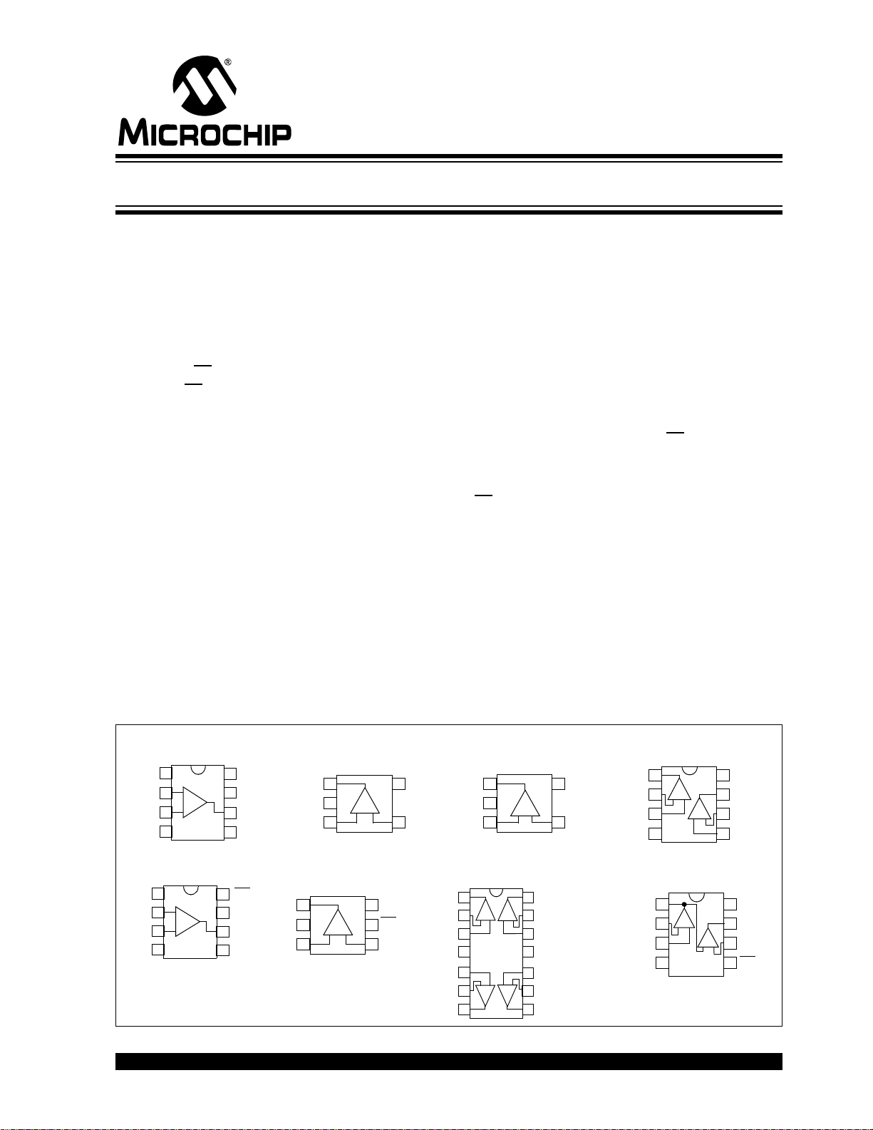
MCP6281/1R/2/3/4/5
V
IN
_
MCP6281
V
DD
1
2
3
4
8
7
6
5
+
NC
NC
NC
V
IN
+
V
SS
MCP6282
PDIP, SOIC, MSOP
MCP6284
1
2
3
4
14
13
12
11
-
+
-
+
10
9
8
5
6
7
+
-
-
+
PDIP, SOIC, TSSOP
1
2
3
4
8
7
6
5
+
-
+
V
OUT
MCP6283
1
2
3
4
8
7
6
5
+
V
INA
_
V
INA
+
V
SS
V
OUTA
V
OUTB
V
DD
V
INB
_
V
INB
+
V
SS
VIN+
V
IN
_
NC
CS
V
DD
V
OUT
NC
V
OUTA
V
INA
_
V
INA
+
V
DD
V
SS
V
OUTB
V
INB
_
V
INB
+
V
OUTC
V
INC
_
V
INC
+
V
OUTD
V
IND
_
V
IND
+
PDIP, SOIC, MSOP
PDIP, SOIC, MSOP
MCP6285
PDIP, SOIC, MSOP
1
2
3
4
8
7
6
5
+
-
V
INA
_
V
INA
+
V
SS
V
OUTA/VINB
+
V
OUTB
V
DD
V
INB
_
CS
-
+
MCP6281
SOT-23-5
4
1
2
3
-
+
5
V
DD
VIN–
V
OUT
V
SS
VIN+
MCP6281R
SOT-23-5
4
1
2
3
-
+
5
V
SS
VIN–
V
OUT
V
DD
VIN+
MCP6283
SOT-23-6
4
1
2
3
-
+
6
5
V
SS
VIN+
V
OUT
CS
V
DD
V
IN
_
450 µA, 5 MHz Rail-to-Rail Op Amp
Features
• Gain Bandwidth Product: 5 MHz (typical)
• Supply Current: IQ = 450 µA (typical)
• Supply Voltage: 2.2V to 6.0V
• Rail-to-Rail Input/Output
• Extended Temperature Range: -40°C to +125°C
• Available in Single, Dual, and Quad Packages
• Single with C
S (MCP6283)
• Dual with CS (MCP6285)
Applications
• Automotive
• Portable Equipment
• Photodiode Amplifier
• Analog Filters
• Notebooks and PDAs
• Battery-Powered Systems
Design Aids
• SPICE Macro Models
• FilterLab® Software
• Mindi™ Circuit Designer & Simulator
• MAPS (Microchip Advanced Part Selector)
• Analog Demonstration and Evaluation Boards
• Application Notes
Description
The Microchip Technology Inc. MCP6281/1R/2/3/4/5
family of operational amplif iers (op amps) provide wi de
bandwidth for the current. This family has a 5 MHz Gain
Bandwidth Product (GBWP) and a 65° phase margin.
This family also operates from a single supply voltage
as low as 2.2V, while drawing 450 µA (typical) quiescent
current. Additionally, the MCP6281/1R/2/3/4/5 supports
rail-to-rail input and output swing, with a common mode
input voltage range of V
This family of operational amplifiers is designed with
Microchip’s advanced CMOS process.
The MCP6285 has a Chip Select (CS) input for dual op
amps in an 8-pin package. This device is manufactured
by cascading the two op amps (the output of op amp A
connected to the non-inverting input of op amp B). The
input puts the device in Low-power mode.
CS
The MCP6281/1R/2/3/4/5 family operates over the
Extended Temperature Range of -40°C to +125°C. It
also has a power supply range of 2.2V to 6.0V.
+300mV to VSS– 300 mV.
DD
Package Types
© 2008 Microchip Technology Inc. DS21811E-page 1
Page 2
MCP6281/1R/2/3/4/5
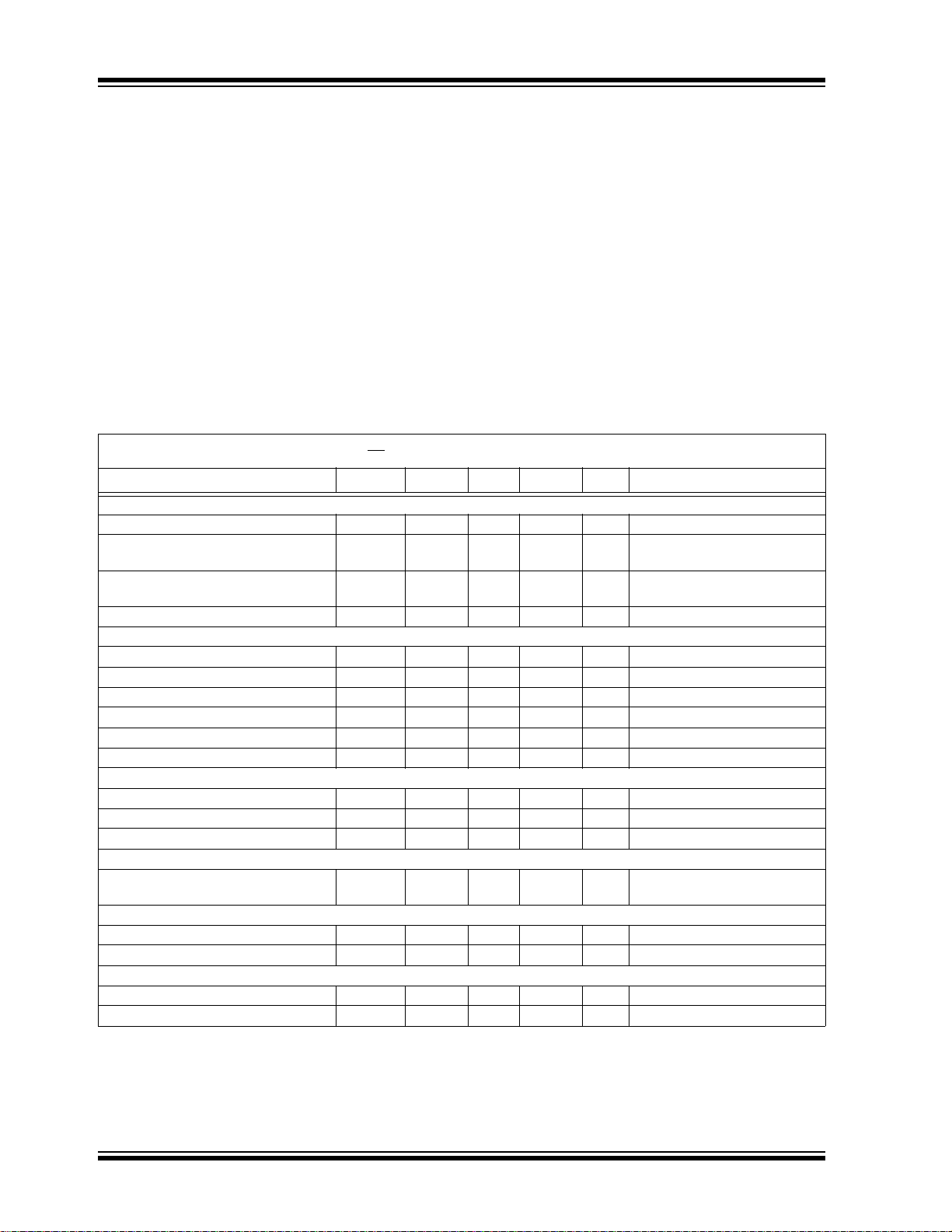
1.0 ELECTRICAL CHARACTERISTICS
† Notice: Stresses above those listed under “Absolute
Maximum Ratings” may cause permanent damage to the
device. This is a stress rating only and functional operation of
the device at those or any other conditions above those
Absolute Maximum Ratings †
VDD–VSS........................................................................7.0V
Current at Input Pins ....................................................±2 mA
Analog Inputs (V
All Other Inputs and Outputs ......... V
Difference Input Voltage ...................................... |V
+, VIN–) ††........ VSS–1.0VtoVDD+1.0V
IN
– 0.3V to VDD+0.3V
SS
DD–VSS
|
indicated in the operational listings of this specification is not
implied. Exposure to maximum rating conditions for extended
periods may affect device reliability.
†† See Section 4.1.2 “Input Voltage and Current Limits”.
Output Short Circuit Current .................................Continuous
Current at Output and Supply Pins ............................±30 mA
Storage Temperature....................................–65°C to +150°C
Maximum Junction Temperature (T
)..........................+150°C
J
ESD Protection On All Pins (HBM; MM).............. ≥ 4 kV; 400V
DC ELECTRICAL SPECIFICATIONS
Electrical Characteristics: Unless otherwise indicated, TA = +25 C, VDD= +2.2V to +5.5V, VSS=GND, V
V
= VDD/2, VL = VDD/2, RL = 10 kΩ to VL and CS is tied low. (refer to Figure 1-2 and Figure 1-3).
CM
Parameters Sym Min Typ Max Units Conditions
Input Offset
Input Offset Voltage V
Input Offset Voltage
OS
V
OS
(Extended Temperature)
Input Offset Temperature Drift ΔV
OS
/ΔT
Power Supply Rejection Ratio PSRR 70 90 — dB V
Input Bias, Input Offset Current and Impedance
Input Bias Current I
At Temperature I
At Temperature I
Input Offset Current I
Common Mode Input Impedance Z
Differential Input Impedance Z
B
B
B
OS
CM
DIFF
Common Mode (Note 4)
Common Mode Input Range V
CMR
Common Mode Rejection Ratio CMRR 70 85 — dB V
Common Mode Rejection Ratio CMRR 65 80 — dB V
Open-Loop Gain
DC Open-Loop Gain (Large Signal) A
OL
Output
Maximum Output Voltage Swing V
Output Short Circuit Current I
, VOHV
OL
SC
Power Supply
Supply Voltage V
Quiescent Current per Amplifier I
Note 1: The MCP6285’s V
for op amp B (pins V
CM
2: The current at the MCP6285’s V
DD
Q
– pin is specified by IB only.
INB
3: This specification does not apply to the MCP6285’s V
4: The MCP6285’s V
The MCP6285’s V
– pin (op amp B) has a common mode range (V
INB
OUTA/VINB
+ pin (op amp B) has a voltage range specified by VOH and VOL.
5: All parts with date codes November 2007 and later have been screened to ensure operation at V
the other minimum and maximum specifications are measured at 2.4V and/or 5.5V.
-3.0 — +3.0 mV VCM = VSS (Note 1)
-5.0 — +5.0 mV TA= -40°C to +125°C,
V
= V
CM
—±1.7—µV/°CT
A
= -40°C to +125°C,
A
V
= VSS (Note 1)
CM
= VSS (Note 1)
CM
— ±1.0 — pA Note 2
— 50 200 pA TA= +85°C (Note 2)
—2 5nAT
= +125°C (Note 2)
A
— ±1.0 — pA Note 3
—1013||6 — Ω||pF Note 3
—1013||3 — Ω||pF Note 3
V
− 0.3 — V
SS
90 110 — dB V
+ 15 — V
SS
+ 0.3 V
DD
= -0.3V to 2.5V, V
CM
= -0.3V to 5.3V, V
CM
= 0.2V to VDD – 0.2V,
OUT
V
CM=VSS
– 15 mV 0.5V input overdrive
DD
—±25—mA
2.2 — 6.0 V (Note 5)
300 450 570 µA IO = 0
OUTA/VINB
+ and V
OUTA/VINB
–) is VSS + 100 mV.
INB
+ pin.
) of VSS + 100 mV to VDD – 100 mV.
CMR
≈ VDD/2,
OUT
(Note 1)
SS
(Note 1)
= 6.0V. However,
DD
DD
DD
= 5V
= 5V
DS21811E-page 2 © 2008 Microchip Technology Inc.
Page 3
MCP6281/1R/2/3/4/5
V
IL
Hi-Z
t
ON
V
IH
CS
t
OFF
V
OUT
-0.7 µA
Hi-Z
I
SS
I
CS
0.7 µA
0.7 µA
-0.7 µA
-450 µA
10 nA
(typical)
(typical)
(typical)
(typical)
(typical)
(typical)
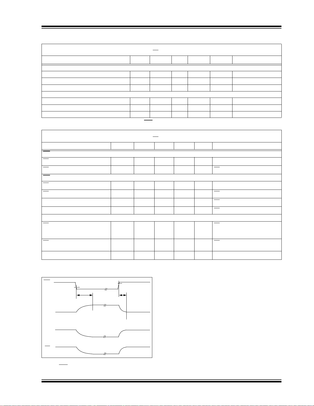
AC ELECTRICAL SPECIFICATIONS
Electrical Characteristics: Unless otherwise indicated, TA = +25°C, VDD = +2.2V to +5.5V, VSS = GND, V
V
= VDD/2, VL = VDD/2, RL = 10 kΩ to VL, CL = 60 pF and CS is tied low. (refer to Figure1-2 and Figure 1-3).
CM
Parameters Sym Min Typ Max Units Conditions
AC Response
Gain Bandwidth Product GBWP — 5.0 — MHz
Phase Margin at Unity-Gain PM — 65 — ° G = +1 V/V
Slew Rate SR — 2.5 — V/µs
Noise
Input Noise Voltage E
Input Noise Voltage Density e
Input Noise Current Density i
ni
ni
ni
—5.2— µV
P-P
—16—nV/√Hz f = 1 kHz
—3—fA/√Hz f = 1 kHz
MCP6283/MCP6285 CHIP SELECT (CS) SPECIFICATIONS
≈ VDD/2,
OUT
f = 0.1 Hz to 10 Hz
Electrical Characteristics: Unless otherwise indicated, T
V
= VDD/2, VL = VDD/2, RL = 10 kΩ to VL, CL = 60 pF and CS is tied low. (refer to Figure1-2 and Figure 1-3).
CM
= +25°C, VDD = +2.2V to +5.5V, VSS = GND, V
A
Parameters Sym Min Typ Max Units Conditions
Low Specifications
CS
Logic Threshold, Low V
CS
Input Current, Low I
CS
IL
CSL
V
SS
—0.2VDDV
—0.01—µACS = V
CS High Specifications
Logic Threshold, High V
CS
Input Current, High I
CS
GND Current per Amplifier I
CSH
SS
0.8 V
IH
DD
—VDDV
—0.7 2µACS = V
—-0.7—µACS = V
Amplifier Output Leakage — — 0.01 — µA CS = V
Dynamic Specifications (Note 1)
Low to Valid Amplifier
CS
Output, Turn-on Time
High to Amplifier Output High-Z t
CS
Hysteresis V
Note 1: The input condition (V
at the output of op amp B (V
t
ON
OFF
HYST
) specified applies to both op amp A and B of the MCP6285. The dynamic specification is tested
IN
OUTB
).
—410µsCS Low ≤ 0.2 VDD, G = +1 V/V,
V
= VDD/2, V
IN
V
= 5.0V
DD
—0.01— µsCS High ≥ 0.8 VDD, G = +1 V/V,
V
= VDD/2, V
IN
—0.6—VV
DD
= 5V
SS
DD
DD
DD
OUT
≈ VDD/2,
OUT
OUT
= 0.9 VDD/2,
= 0.1 VDD/2
FIGURE 1-1: Timing Diagram for the Chip
Select (CS)
© 2008 Microchip Technology Inc. DS21811E-page 3
pin on the MCP6283 and MCP6285.
Page 4
MCP6281/1R/2/3/4/5
V
DD
MCP628X
R
G
R
F
R
N
V
OUT
V
IN
VDD/2
1µF
C
L
R
L
V
L
0.1 µF
V
DD
MCP628X
R
G
R
F
R
N
V
OUT
VDD/2
V
IN
1µF
C
L
R
L
V
L
0.1 µF
TEMPERATURE SPECIFICATIONS
Electrical Characteristics: Unless otherwise indicated, VDD = +2.2V to +5.5V and VSS = GND.
Parameters Sym Min Typ Max Units Conditions
Temperature Ranges
Operating Temperature Range T
Storage Temperature Range T
Thermal Package Resistances
Thermal Resistance, 5L-SOT-23 θ
Thermal Resistance, 6L-SOT-23 θ
Thermal Resistance, 8L-PDIP θ
Thermal Resistance, 8L-SOIC θ
Thermal Resistance, 8L-MSOP θ
Thermal Resistance, 14L-PDIP
Thermal Resistance, 14L-SOIC
Thermal Resistance, 14L-TSSOP
Note: The Junction Temperature (T
) must not exceed the Absolute Maximum specification of +150°C.
J
A
A
JA
JA
JA
JA
JA
θ
JA
θ
JA
θ
JA
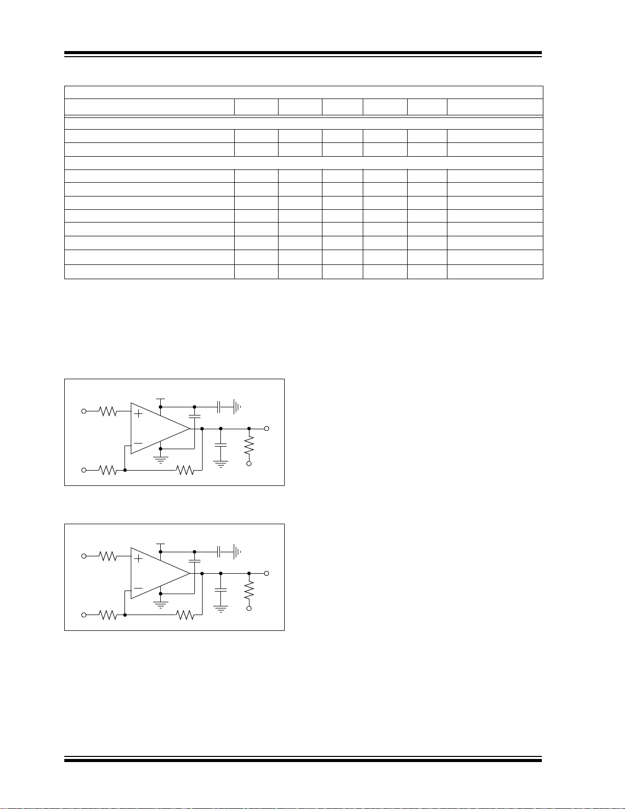
1.1 Test Circuits
The test circuits used for the DC and AC tests are
shown in Figure 1-2 and Figure 1-2. The bypass
capacitors are laid out according to the rules discussed
in Section 4.6 “Supply Bypass”.
-40 — +125 °C Note
-65 — +150 °C
— 256 — °C/W
— 230 — °C/W
—85—°C/W
— 163 — °C/W
— 206 — °C/W
—
—
—
70
120
100
—
—
—
°C/W
°C/W
°C/W
FIGURE 1-2: AC and DC Test Circuit for Most Non-Inverting Gain Conditions.
FIGURE 1-3: AC and DC Test Circuit for Most Inverting Gain Conditions.
DS21811E-page 4 © 2008 Microchip Technology Inc.
Page 5
MCP6281/1R/2/3/4/5
0%
2%
4%
6%
8%
10%
12%
14%
-2.8
-2.4
-2.0
-1.6
-1.2
-0.8
-0.4
0.0
0.4
0.8
1.2
1.6
2.0
2.4
2.8
Input Offset Voltage (mV)
Percentage of Occurrences
832 Samples
V
CM
= V
SS
0%
5%
10%
15%
20%
25%
0 102030405060708090100
Input Bias Current (pA)
Percentage of Occurrences
210 Samples
T
A
= +85°C
-100
-50
0
50
100
150
200
250
300
-0.5 0.0 0.5 1.0 1.5 2.0 2.5
Common Mode Input Voltage (V)
Input Offset Voltage (µV)
VDD = 2.2V
TA = +125°C
T
A
= +85°C
T
A
= +25°C
T
A
= -40°C
0%
5%
10%
15%
20%
25%
30%
-10-8-6-4-20246810
Input Offset Voltage Drift (µV/°C)
Percentage of Occurrences
832 Samples
V
CM
= V
SS
TA = -40°C to +125°C
0%
5%
10%
15%
20%
25%
30%
35%
0
200
400
800
1200
1600
2000
2400
2800
3200
3600
Input Bias Current (pA)
Percentage of Occurrences
210 Samples
T
A
= +125°C
-100
-50
0
50
100
150
200
250
300
-0.5
0.0
0.5
1.0
1.5
2.0
2.5
3.0
3.5
4.0
4.5
5.0
5.5
6.0
Common Mode Input Voltage (V)
Input Offset Voltage (µV)
VDD = 5.5V
TA = +125°C
T
A
= +85°C
T
A
= +25°C
T
A
= -40°C
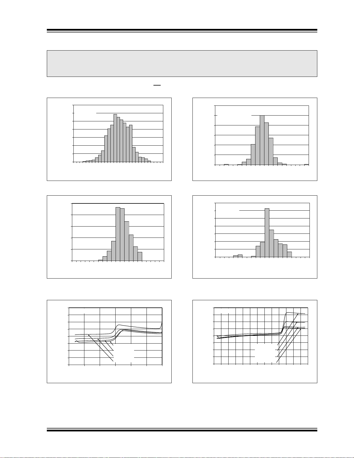
2.0 TYPICAL PERFORMANCE CURVES
Note: The graphs and tables provided following this note are a statistical summary based on a limited number of
samples and are provided for informational purposes only. The performance characteristics listed herein
are not tested or guaranteed. In some graphs or tables, the data presented may be outside the specified
operating range (e.g., outside specified power supply range) and therefore outside the warranted range.
Note: Unless otherwise indicated, TA = +25°C, VDD = +2.2V to +6.0V, VSS = GND, VCM = VDD/2, V
= VDD/2, RL = 10 kΩ to VL, CL = 60 pF and CS is tied low.
V
L
OUT
≈ VDD/2,
FIGURE 2-1: Input Offset Voltage.
FIGURE 2-2: Input Bias Current at
=+85 °C.
T
A
FIGURE 2-4: Input Offset Voltage Drift.
FIGURE 2-5: Input Bias Current at
= +125 °C.
T
A
FIGURE 2-3: Input Offset Voltage vs.
Common Mode Input Voltage at V
© 2008 Microchip Technology Inc. DS21811E-page 5
FIGURE 2-6: Input Offset Voltage vs.
= 2.2V.
DD
Common Mode Input Voltage at V
= 5.5V.
DD
Page 6
MCP6281/1R/2/3/4/5
-100
-50
0
50
100
150
200
250
300
0.0 0.5 1.0 1.5 2.0 2.5 3.0 3.5 4.0 4.5 5.0 5.5
Output Voltage (V)
Input Offset Voltage (µV)
VDD = 2.2V
VCM = V
SS
Representative Part
VDD = 5.5V
20
30
40
50
60
70
80
90
100
110
1.E+00 1.E+01 1.E+ 02 1.E+03 1.E+04 1.E+05 1.E+06
Frequency (Hz)
CMRR, PSRR (dB)
1 10k 100k 1M10010 1k
PSRR+
PSRR-
CMRR
-25
-15
-5
5
15
25
35
45
55
0.0 0.5 1.0 1.5 2.0 2.5 3.0 3.5 4.0 4.5 5.0 5.5
Common Mode Input Voltage (V)
Input Bias, Offset Currents
(pA)
TA = +85°C
V
DD
= 5.5V
Input Bias Current
Input Offset Current
1
10
100
1,000
10,000
25 35 45 55 65 75 85 95 105 115 125
Ambient Temperature (°C)
Input Bias, Offset Currents
(pA)
Input Bias Current
Input Offset Current
VCM = V
DD
VDD = 5.5V
60
70
80
90
100
110
120
-50 -25 0 25 50 75 100 125
Ambient Temperature (°C)
PSRR, CMRR (dB)
PSRR
V
CM
= V
SS
CMRR
-1.0
-0.5
0.0
0.5
1.0
1.5
2.0
2.5
0.0 0.5 1.0 1.5 2.0 2.5 3.0 3.5 4.0 4.5 5.0 5.5
Common Mode Input Voltage (V)
Input Bias, Offset Currents
(nA)
TA = +125°C
V
DD
= 5.5V
Input Bias Current
Input Offset Current
TYPICAL PERFORMANCE CURVES (CONTINUED)
Note: Unless otherwise indicated, TA = +25°C, VDD = +2.2V to +6.0V, VSS = GND, VCM = VDD/2, V
VL = VDD/2, RL = 10 kΩ to VL, CL = 60 pF and CS is tied low.
OUT
≈ VDD/2,
FIGURE 2-7: Input Offset Voltage vs. Output Voltage.
FIGURE 2-8: CMRR, PSRR vs. Frequency.
FIGURE 2-10: Input Bias, Input Offset Currents vs. Ambient Temperature.
FIGURE 2-11: CMRR, PSRR vs. Ambient Temperature.
FIGURE 2-9: Input Bias, Offset Currents
vs. Common Mode Input Voltage at T
DS21811E-page 6 © 2008 Microchip Technology Inc.
=+85°C.
A
FIGURE 2-12: Input Bias, Offset Currents
vs. Common Mode Input Voltag e at TA= +125°C.
Page 7
MCP6281/1R/2/3/4/5
0
100
200
300
400
500
600
0.0 0.5 1.0 1.5 2.0 2.5 3.0 3.5 4.0 4.5 5.0
5
Power Supply Voltage (V)
Quiescent Current
(µA/amplifier)
TA = +125°C
T
A
= +85°C
T
A
= +25°C
T
A
= -40°C
-20
0
20
40
60
80
100
120
1.E-01
1.E+00
1.E+01
1.E+02
1.E+03
1.E+04
1.E+05
1.E+06
1.E+07
1.E+08
Frequency (Hz)
Open-Loop Gain (dB)
-210
-180
-150
-120
-90
-60
-30
0
Open-Loop Phase (°)
Gain
Phase
0.1
1 10 100 1k 10k 100k 1M 10M 100M
0.1
1
10
1.E+03
1.E+04
1.E+05
1.E+06
1.E+07
Frequency (Hz)
Swing (V
P-P
)
VDD = 2.2V
1k 10k 100k 1M
VDD = 5.5V
10M
1
10
100
1000
0.01 0.1 1 10
Output Current Magnitude (mA)
Ouput Voltage Headroom (mV)
VOL - V
SS
VDD - V
OH
0
1
2
3
4
5
6
-50-250 255075100125
Ambient Temperature (°C)
(MHz)
60
65
70
75
80
85
90
Phase Margin (°)
VDD = 5.5V
VDD = 2.2V
VDD = 2.2V
VDD = 5.5V
0.0
0.5
1.0
1.5
2.0
2.5
3.0
3.5
4.0
4.5
-50 -25 0 25 50 75 100 125
Ambient Temperature (°C)
Slew Rate (V/µs)
Rising Edge, VDD = 2.2V
Rising Edge, VDD = 5.5V
Falling Edge, VDD = 5.5V
Falling Edge, VDD = 2.2V
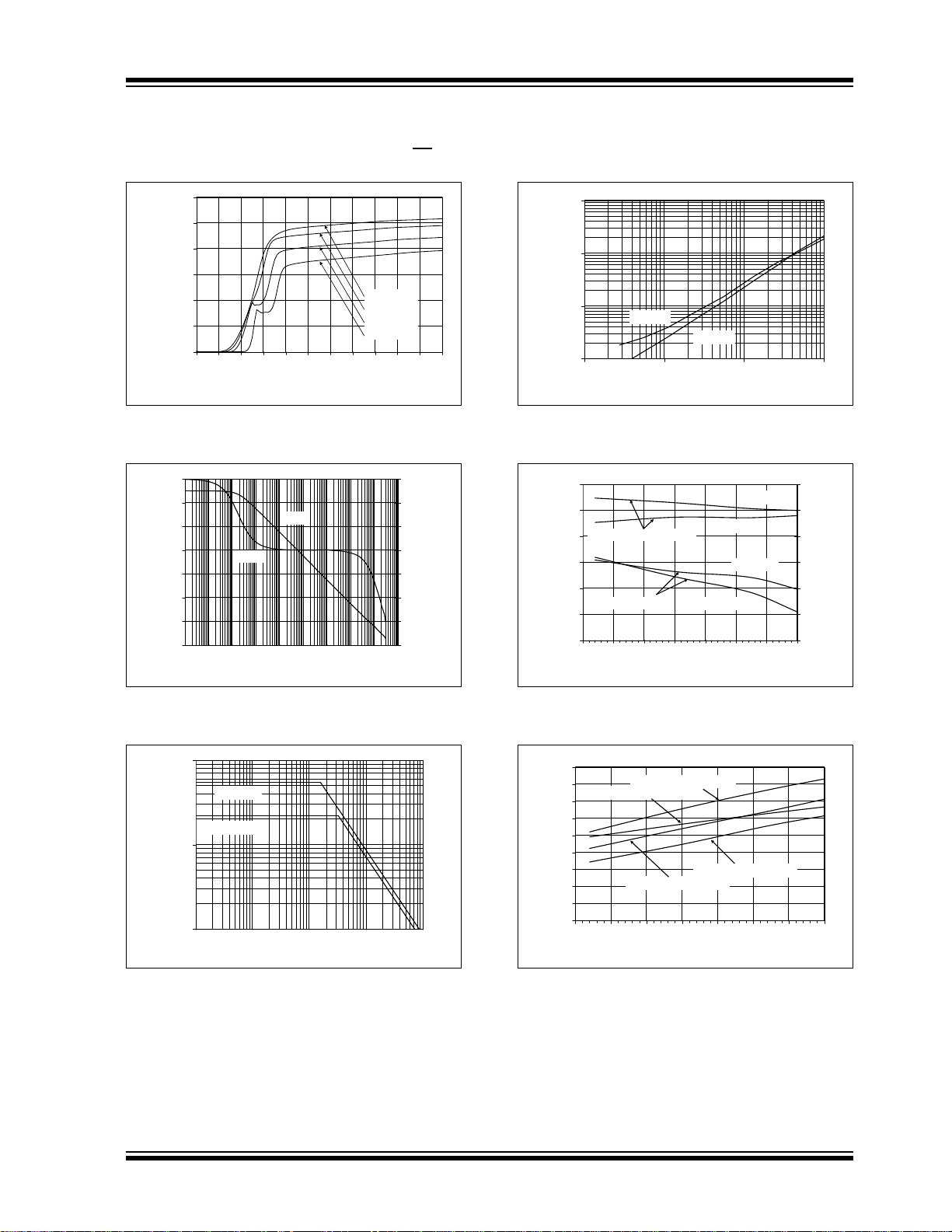
TYPICAL PERFORMANCE CURVES (CONTINUED)
Note: Unless otherwise indicated, TA = +25°C, VDD = +2.2V to +6.0V, VSS = GND, VCM = VDD/2, V
VL = VDD/2, RL = 10 kΩ to VL, CL = 60 pF and CS is tied low.
5.
OUT
≈ VDD/2,
FIGURE 2-13: Quiescent Current vs. Power Supply Voltage.
FIGURE 2-14: Open-Loop Gain, Phase vs. Frequency.
FIGURE 2-16: Output Voltage Headroom vs. Output Current Magnitude.
Gain Bandwidth Product
Phase Margin
Gain Bandwidth Product
FIGURE 2-17: Gain Bandwidth Product, Phase Margin vs. Ambient Temperature.
Maximum Output Voltage
FIGURE 2-15: Maximum Output Voltage Swing vs. Frequency.
© 2008 Microchip Technology Inc. DS21811E-page 7
FIGURE 2-18: Slew Rate vs. Ambient Temperature.
Page 8
MCP6281/1R/2/3/4/5
10
100
1,000
1.E-01 1.E+00 1.E+01 1.E+02 1.E+03 1.E+04 1.E+05 1.E+06
Frequency (Hz)
Input Noise Voltage Density
(nV/
√
Hz)
0.1 10010 1k 100k10k 1M1
0
5
10
15
20
25
30
35
0.00.51.01.52.02.53.03.54.04.55.05.5
Power Supply Voltage (V)
(mA)
TA = +125°C
T
A
= +85°C
T
A
= +25°C
T
A
= -40°C
0
50
100
150
200
250
300
350
400
450
500
0.0 0.2 0.4 0.6 0.8 1.0 1.2 1.4 1.6 1.8 2.0 2.2
Chip Select Voltage (V)
(µA/Amplifier)
Hysteresis
Op-Amp shuts off here
Op-Amp turns on here
VDD = 2.2V
CS swept
high to low
CS swept
low to high
0
5
10
15
20
25
30
0.0 0.5 1.0 1.5 2.0 2.5 3.0 3.5 4.0 4.5 5.0
Common Mode Input Voltage (V)
Input Noise Voltage Density
(nV/
√
Hz)
f = 1 kHz
V
DD
= 5.0V
100
110
120
130
140
1 10 100
Frequency (kHz)
(dB)
0
100
200
300
400
500
600
700
800
900
1000
0.0 0.5 1.0 1.5 2.0 2.5 3.0 3.5 4.0 4.5 5.0 5.5
Chip Select Voltage (V)
(µA/Amplifier)
Hysteresis
Op Amp toggles On/Off here
VDD = 5.5V
CS swept
low to high
CS swept
high to low
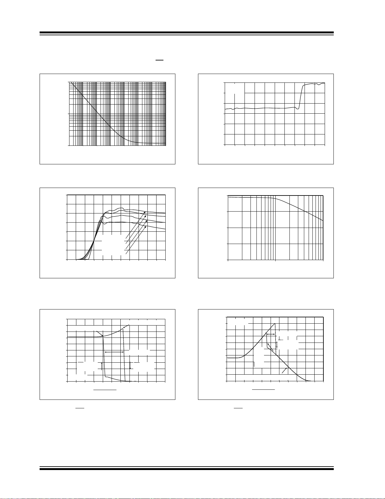
TYPICAL PERFORMANCE CURVES (CONTINUED)
Note: Unless otherwise indicated, TA = +25°C, VDD = +2.2V to +6.0V, VSS = GND, VCM = VDD/2, V
VL = VDD/2, RL = 10 kΩ to VL, CL = 60 pF and CS is tied low.
OUT
≈ VDD/2,
FIGURE 2-19: Input Noise Voltage Density vs. Frequency.
Ouptut Short Circuit Current
FIGURE 2-20: Output Short Circuit Current vs. Power Supply Voltage.
FIGURE 2-22: Input Noise Voltage Density vs. Common Mode Input Voltage at 1 kHz.
Channel-to-Channel Separation
FIGURE 2-23: Channel-to-Channel Separation vs. Frequency (MCP6282 and MCP6284 only).
Quiescent Current
FIGURE 2-21: Quiescent Current vs.
Chip Select (CS
(MCP6283 and MCP6285 only).
DS21811E-page 8 © 2008 Microchip Technology Inc.
) Voltage at VDD = 2.2V
Quiescent Current
FIGURE 2-24: Quiescent Current vs. Chip Select (CS) Voltage at VDD = 5.5V (MCP6283 and MCP6285 only).
Page 9
MCP6281/1R/2/3/4/5
0.0
0.5
1.0
1.5
2.0
2.5
3.0
3.5
4.0
4.5
5.0
0.E+00 2.E-06 4.E-06 6.E-06 8.E-06 1.E-05 1.E-05 1.E-05 2.E-05 2.E-05 2.E-05
Time (2 µs/div)
Output Voltage (V)
G = +1V/V
V
DD
= 5.0V
Time (500 ns/div)
Output Voltage (10 mV/div)
G = +1V/V
0.0
0.5
1.0
1.5
2.0
2.5
0.0E+00 5.0E-06 1.0E-05 1.5E-05 2.0E-05 2.5E-05 3.0E-05 3.5E-05 4.0E-05 4.5E-05 5.0E-05
Time (5 µs/div)
Chip Select, Output Voltages
(V)
V
OUT
Output On
Output High-Z
VDD = 2.2V
G = +1V/V
V
IN
= V
SS
CS Voltage
0.0
0.5
1.0
1.5
2.0
2.5
3.0
3.5
4.0
4.5
5.0
0.E+00 2.E-06 4.E-06 6.E-06 8 .E-06 1.E-05 1.E-05 1.E-05 2.E-05 2.E-05 2.E-05
Time (2 µs/div)
Output Voltage (V)
G = -1V/V
V
DD
= 5.0V
Time (500 ns/div)
Output Voltage (10 mV/div)
G = -1V/V
0.0
0.5
1.0
1.5
2.0
2.5
3.0
3.5
4.0
4.5
5.0
5.5
6.0
0.E+00 5.E-06 1.E-05 2.E-05 2.E-05 3.E-05 3.E-05 4.E-05 4.E-05 5.E-05 5.E-05
Time (5 µs/div)
Chip Select, Output Voltages
(V)
V
OUT
Output OnOutput High-Z
VDD = 5.5V
G = +1V/V
V
IN
= V
SS
CS Voltage
TYPICAL PERFORMANCE CURVES (CONTINUED)
Note: Unless otherwise indicated, TA = +25°C, VDD = +2.2V to +6.0V, VSS = GND, VCM = VDD/2, V
VL = VDD/2, RL = 10 kΩ to VL, CL = 60 pF and CS is tied low.
OUT
≈ VDD/2,
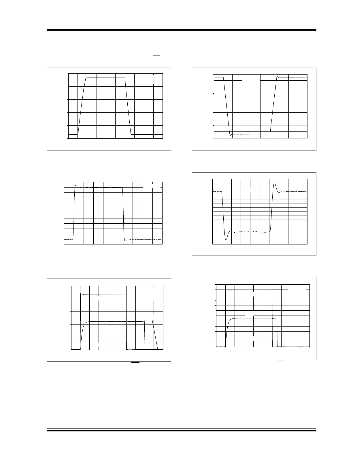
FIGURE 2-25: Large-Signal, Non-inverting Pulse Response.
FIGURE 2-26: Small-Signal, Non-inverting Pulse Response.
FIGURE 2-28: Large-Signal, Inverting Pulse Response.
FIGURE 2-29: Small-Signal, Inverting Pulse Response.
FIGURE 2-27: Chip Select (CS
Amplifier Output Response Time at V
(MCP6283 and MCP6285 only).
© 2008 Microchip Technology Inc. DS21811E-page 9
) to
= 2.2V
DD
FIGURE 2-30: Chip Select (CS
Amplifier Output Response Time at V
(MCP6283 and MCP6285 only).
) to
DD
= 5.5V
Page 10
MCP6281/1R/2/3/4/5
1.E-12
1.E-11
1.E-10
1.E-09
1.E-08
1.E-07
1.E-06
1.E-05
1.E-04
1.E-03
1.E-02
-1.0 -0.9 -0.8 -0.7 -0.6 -0.5 -0.4 -0.3 -0.2 -0.1 0.0
Input Voltage (V)
Input Current Magnitude (A)
10m
1m
100µ
10µ
1µ
100n
10n
1n
100p
10p
1p
-1
0
1
2
3
4
5
6
-15 -14 -13 -12 -11 -10 -9 -8 -7 -6 -5
Time (1 ms/div)
Input, Output Voltage (V)
VDD = 5.0V
G = +2 V/V
V
IN
V
OUT
Note: Unless otherwise indicated, TA = +25°C, VDD = +2.2V to +6.0V, VSS = GND, VCM = VDD/2, V
VL = VDD/2, RL = 10 kΩ to VL, CL = 60 pF and CS is tied low.
+125°C
+85°C
+25°C
-40°C
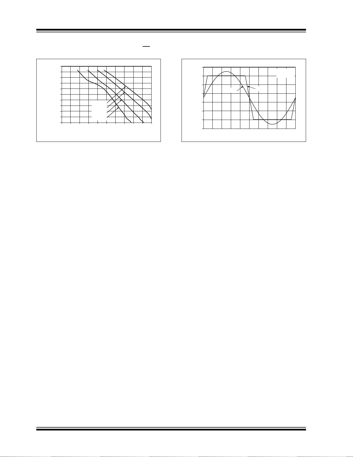
FIGURE 2-31: Measured Input Current vs.
Input Voltage (below V
SS
).
FIGURE 2-32: The MCP6281/1R/2/3/4/5 Show No Phase Reversal.
OUT
≈ VDD/2,
DS21811E-page 10 © 2008 Microchip Technology Inc.
Page 11
MCP6281/1R/2/3/4/5
3.0 PIN DESCRIPTIONS
Descriptions of the pins are listed in Table 3-1 (single op amps) and Table 3-2 (dual and quad op amps).
TABLE 3-1: PIN FUNCTION TABLE FOR SINGLE OP AMPS
MCP6281 MCP6281R MCP6283
PDIP, SOIC,
MSOP
SOT-23-5 SOT-23-5
PDIP, SOIC,
MSOP
SOT-23-6
611 6 1V
244 2 4V
333 3 3V
752 7 6V
425 4 2V
——— 8 5CS
1,5,8 — — 1,5 — NC No Internal Connection
TABLE 3-2: PIN FUNCTION TABLE FOR DUAL AND QUAD OP AMPS
MCP6282 MCP6284 MCP6285
PDIP, SOIC, MSOP
11—V
222V
333V
848V
55—V
666V
777V
—8—V
—9—V
—10—V
4114V
—12—V
—13—V
—14—V
—— 1V
—— 5CS
PDIP, SOIC, TSSOP
PDIP, SOIC, MSOP
Symbol Description
Analog Output
OUT
– Inverting Input
IN
+ Non-inverting Input
IN
Positive Power Supply
DD
Negative Power Supply
SS
Chip Select
Symbol Description
Analog Output (op amp A)
OUTA
– Inverting Input (op amp A)
INA
+ Non-inverting Input (op amp A)
INA
Positive Power Supply
DD
+ Non-inverting Input (op amp B)
INB
– Inverting Input (op amp B)
INB
Analog Output (op amp B)
OUTB
Analog Output (op amp C)
OUTC
– Inverting Input (op amp C)
INC
+ Non-inverting Input (op amp C)
INC
Negative Power Supply
SS
+ Non-inverting Input (op amp D)
IND
– Inverting Input (op amp D)
IND
Analog Output (op amp D)
OUTD
/
OUTA
V
Analog Output (op amp A)/Non-
+
inverting Input (op amp B)
INB
Chip Select
3.1 Analog Outputs
The output pins are low-impedance voltage sources.
3.4 Chip Select Digital Input (CS)
This is a CMOS, Schmitt-triggered input that places the
part into a low-power mode of operation.
3.2 Analog Inputs
The non-inverting and inverting inputs are highimpedance CMOS inputs with low bias currents.
3.3 MCP6285’s V
OUTA/VINB
For the MCP6285 only, the output of op amp A is
connected directly to the non-inverting input of
op amp B; this is the V
OUTA/VINB
+ Pin
+ pin. This connection
3.5 Power Supply Pins
The positive power supply (VDD) is 2.2V to 6.0V higher
than the negative power supply (V
operation, the other pins are between V
Typically, these parts are used in a single (positive)
supply configuration. In this case, V
ground and V
is connected to the supply. VDD will
DD
need bypass capacitors.
). For normal
SS
and VDD.
SS
is connected to
SS
makes it possible to provide a Chip Select pin for duals
in 8-pin packages.
© 2008 Microchip Technology Inc. DS21811E-page 11
Page 12

MCP6281/1R/2/3/4/5
Bond
Pad
Bond
Pad
Bond
Pad
V
DD
VIN+
V
SS
Input
Stage
Bond
Pad
VIN–
V
1
MCP628X
R
1
V
DD
D
1
R1>
VSS– (minimum expected V1)
2mA
R
2
>
VSS– (minimum expected V2)
2mA
V
2
R
2
D
2
R
3
4.0 APPLICATION INFORMATION
The MCP6281/1R/2/3/4/5 family of op amps is manufactured using Microchip's state-of-the-art CMOS
process. This family is specifically designed for lowcost, low-power and general purpose applications.
The low supply voltage, low quiescent current and
wide bandwidth makes the MCP6281/1R/2/3/4/5 ideal
for battery-powered applications.
4.1 Rail-to-Rail Inputs
4.1.1 PHASE REVERSAL
The MCP6281/1R/2/3/4/5 op amp is designed to
prevent phase reversal when the input pins exceed the
supply voltages. Figure 2-32 shows the input voltage
exceeding the supply voltage without any phase
reversal.
4.1.2 INPUT VOLTAGE AND CURRENT
LIMITS
The ESD protection on the inputs can be depicted as
shown in Figure 4-1. This structure was chosen to
protect the input transistors, and to minimize input bias
current (I
when they try to go more than one diode drop below
V
SS
above VDD; their breakdown voltage is high enough to
allow normal operation, and low enough to bypass
quick ESD events within the specified limits.
). The input ESD diodes clamp the inputs
B
. They also clamp any voltages that go too far
V
, and dump any currents onto VDD. When
DD
implemented as shown, resistors R1 and R2 also limit
the current through D1 and D2.
FIGURE 4-2: Protecting the Analog Inputs.
It is also possible to connect the diodes to the left of
resistors R
diodes D1 and D2 needs to be limited by some other
mechanism. The resistors then serve as in-rush current
limiters; the DC current into the input pins (V
VIN–) should be very small.
A significant amount of current can flow out of the
inputs when the common mode voltage (V
ground (V
high impedance may need to limit the usable voltage
range.
and R2. In this case, current through the
1
+ and
IN
) is below
); see Figure 2-31. Applications that are
SS
CM
FIGURE 4-1: Simplified Analog Input ESD Structures.
In order to prevent damage and/or improper operation
of these op amps, the circuit they are in must limit the
currents and voltages at the V
Absolute Maximum Ratings † at the beginning of
Section 1.0 “Electrical Characteristics”). Figure 4-2
shows the recommended approach to protecting these
inputs. The internal ESD diodes prevent the input pins
(V
the resistors R
out of the input pins. Diodes D
input pins (VIN+ and VIN–) from going too far above
DS21811E-page 12 © 2008 Microchip Technology Inc.
+ and VIN–) from going too far below ground, and
IN
and R2 limit the possible current drawn
1
+ and VIN– pins (see
IN
and D2 prevent the
1
4.1.3 NORMAL OPERATION
The input stage of the MCP6281/1R/2/3/4/5 op amps
use two differential CMOS input stages in parallel. One
operates at low common mode input voltage (V
while the other operates at high V
topology, the device operates with V
. WIth this
CM
up to 0.3V
CM
above VDD and 0.3V below VSS.
There is a transition in input behavior as V
changed. It occurs when V
is near VDD–1.2V (see
CM
Figure 2-3 and Figure 2-6). For the best distortion
performance with non-inverting gains, avoid these
regions of operation.
CM
CM
is
),
Page 13

MCP6281/1R/2/3/4/5
V
IN
R
ISO
V
OUT
C
L
–
+
MCP628X
10
100
1,000
10 100 1,000 10,000
Normalized Load Capacitance; C
L
/ GN (pF)
Recommended R
ISO
(
:
)
GN = 1 V/V
G
N
= 2 V/V
G
N
t 4 V/V
A
B
CS
2
3
5
6
7
V
INA
+
V
OUTB
MCP6285
1
V
INA
–
V
OUTA/VINB
+
V
INB
–
4.2 Rail-to-Rail Output
The output voltage range of the MCP6281/1R/2/3/4/5
op amp is V
–15mV (min.) and VSS+15mV (max.)
DD
when RL=10kΩ is connected to VDD/2 and
VDD= 5.5V. Refer to Figure 2-16 for more information.
4.3 Capacitive Loads
Driving large capacitive loads can cause stability
problems for voltage feedback op amps. As the load
capacitance increases, the feedback loop’s phase
margin decreases and the closed-loop bandwidth is
reduced. This produces gain peaking in the frequency
response, with overshoot and ringing in the step
response. A unity-gain buffer (G = +1) is the most
sensitive to capacitive loads, though all gains show the
same general behavior.
When driving large capacitive loads with these op
amps (e.g., > 100 pF when G = +1), a small series
resistor at the output (R
feedback loop’s phase margin (stability) by making the
output load resistive at higher frequencies. The
bandwidth will generally be lower than the bandwidth
with no capacitive load.
in Figure 4-3) improves the
ISO
After selecting R
for your circuit, double-check the
ISO
resulting frequency response peaking and step
response overshoot. Modify R
's value until the
ISO
response is reasonable. Bench evaluation and si mulations with the MCP6281/1R/2/3/4/5 SPICE macro
model are helpful.
4.4 MCP628X Chip Select (CS)
The MCP6283 and MCP6285 are single and dual op
amps with Chip Select (CS), respectively. When CS is
pulled high, the supply current drops to 0.7 µA (typical)
and flows through the CS
pin to VSS. When this happens, the amplifier output is put into a high-impedance
state. By pulling CS low, the amplifier is enabled . The
pin has an internal 5 MΩ (typical) pull-down resistor
CS
connected to VSS, so it will go low if the CS pin is left
floating. Figure 1-1 shows the output voltage and
supply current response to a CS
pulse.
4.5 Cascaded Dual Op Amps
(MCP6285)
The MCP6285 is a dual op amp with Chip Select (CS).
The Chip Select input is available on w hat would be the
non-inverting input of a standard dual op amp (pin 5).
This pin is available because the output of op am p A
connects to the non-inverting input of op amp B, as
shown in Figure 4-5. The Chip Select input, which can
be connected to a microcontroller I/O line, puts the
device in Low-power mode. Refer to Section 4.4
“MCP628X Chip Select (CS)”.
FIGURE 4-3: Output Resistor, R
stabilizes large capacitive loads.
Figure 4-4 gives recommended R
ent capacitive loads and gains. The x-axis is the
normalized load capacitance (C
circuit's noise gain. For non-inverting gains, G
Signal Gain are equal. For inverting gains, G
1+|Signal Gain| (e.g., -1 V/V gives GN = +2 V/V).
FIGURE 4-4: Recommended R
for Capacitive Loads.
© 2008 Microchip Technology Inc. DS21811E-page 13
ISO
values for differ-
ISO
), where GN is the
L/GN
and the
N
N
is
FIGURE 4-5: Cascaded Gain Amplifier.
The output of op amp A is loaded by the input impedance of op amp B, which is typically 10
specified in the DC specification table (Refer to
Section 4.3 “Capacitive Loads” for further details
regarding capacitive loads).
The common mode input range of these op amps is
specified in the data sheet as V
+ 300 mV. However, since the output of op amp A
V
DD
is limited to V
and VOH (20 mV from the rails with a
OL
10 kΩ load), the non-inverting input range of op amp B
ISO
Values
is limited to the common mode input range of
+ 20 mV and VDD–20mV.
V
SS
13
Ω||6pF, as
– 300 mV and
SS
Page 14

MCP6281/1R/2/3/4/5
V
DD
V
DD
¼ MCP6284 (A) ¼ MCP6284 (B)
R
1
R
2
V
DD
V
REF
V
REFVDD
R
2
R1R2+
------------------
⋅=
Guard Ring
V
SS
VIN–V
IN
+
4.6 Supply Bypass
With this family of operational amplifiers, the power
supply pin (V
bypass capacitor (i.e., 0.01 µF to 0.1 µF) withi n 2 mm
for good, high-frequency performance. It also needs a
bulk capacitor (i.e., 1 µF or larger) within 100 mm to
provide large, slow currents. This bulk capacitor can be
shared with nearby analog parts.
4.7 Unused Op Amps
for single-supply) should have a local
DD
An unused op amp in a quad package (MCP6284)
should be configured as shown in Figure 4-6. These
circuits prevent the output from toggling and causing
crosstalk. Circuits A sets the op amp at its minimum
noise gain. The resistor divider produces any desired
reference voltage within the output voltage range of the
op amp; the op amp buffers that reference voltage.
Circuit B uses the minimum number of components
and operates as a comparator, but it may draw more
current.
FIGURE 4-6: Unused Op Amps.
FIGURE 4-7: Example Guard Ring Layout
for Inverting Gain.
1. For Inverting Gain and Transimpedance
Amplifiers (convert current to voltage, such as
photo detectors):
a. Connect the guard ring to the non-inverting
input pin (V
to the same reference voltage as the op
amp (e.g., V
b. Connect the inverting pin (V
with a wire that does not touch the PCB
surface.
2. Non-inverting Gain and Unity-Gain Buffer:
a. Connect the non-inverting pin (V
input with a wire that does not touch the
PCB surface.
b. Connect the guard ring to the inverting input
pin (V
IN
common mode input voltage.
+). This biases the guard ring
IN
/2 or ground).
DD
–) to the input
IN
+) to the
IN
–). This biases the guard ring to the
4.8 PCB Surface Leakage
In applications where low input bias current i s critical,
Printed Circuit Board (PCB) surface-leakage effects
need to be considered. Surface leakage is caused by
humidity, dust or other contamination on the board.
Under low humidity conditions, a typical resistance
between nearby traces is 10
cause 5 pA of current to flow, which is greater than the
MCP6281/1R/2/3/4/5 family’s bias current at +25°C
(1 pA, typical).
The easiest way to reduce surface leakage is to use a
guard ring around sensitive pins (or traces). The guard
ring is biased at the same voltage as the sensitive pin.
An example of this type of layout is shown in
Figure 4-7.
DS21811E-page 14 © 2008 Microchip Technology Inc.
12
Ω. A 5V difference would
Page 15

MCP6281/1R/2/3/4/5
MCP6281
V
OUT
V
IN
VDD/2
R
2
R
1
C
2
C
1
+
–
MCP6281
V
OUT
V
IN
VDD/2
RC
V
OUT
V
IN
=
1
sRC
SW
+
–
A
B
MCP6285
CS
V
OUTB
Load
V
OUTVINGAGBVOSAGAGBVOSBGB
++=
Where:
G
A
= op amp A gain
G
B
= op amp B gain
V
OSA
= op amp A input offset voltage
V
OSB
= op amp B input offset voltage
4.9 Application Circuits
4.9.1 SALLEN-KEY HIGH-PASS FILTER
The MCP6281/1R/2/3/4/5 op amps can be used in
active-filter applications. Figure 4-8 shows a secondorder Sallen-Key high-pass filter with a gain of 1. The
output bias voltage is set by the V
can be changed to any voltage within the output voltage
range.
FIGURE 4-8: Sallen-Key High-Pass Filter.
This filter, and others, can be designed using
Microchip’s Design Aids; see Section 5.2 “FilterLab®
Software” and Section 5.3 “Mindi™ Circuit
Designer & Simulator”.
/2 reference, which
DD
4.9.3 CASCADED OP AMP
APPLICATIONS
The MCP6285 provides the flexibility of Low-power
mode for dual op amps in an 8-pin package. The
MCP6285 eliminates the added cost and space in
battery-powered applications by using two single op
amps with Chip Select lines or a 10-pin device with one
Chip Select line for both op amps. Since the two op
amps are internally cascaded, this device cannot be
used in circuits that require active or passive elements
between the two op amps. However, there are several
applications where this op amp configuration with
Chip Select line becomes suitable. The circuits below
show possible applications for this device.
4.9.3.1 Load Isolation
With the cascaded op amp configuration, op amp B can
be used to isolate the load from op amp A. In applications where op amp A is driving capacitive or low resistance loads in the feedback loop (such as an integrator
circuit or filter circuit), the op amp may not have
sufficient source current to drive the load. In this case,
op amp B can be used as a buffer.
4.9.2 INVERTING MILLER INTEGRATOR
Analog integrators are used in filters, control loops and
measurement circuits. Figure 4-9 shows the most
common implementation, the inverting Miller integrator.
The non-inverting input is at V
/2 so that the op amp
DD
properly biases up. The switch (SW) is used to zero the
output in some applications. Other applications use a
feedback loop to keep the output within its linear range
of operation.
FIGURE 4-9: Miller Integrator.
FIGURE 4-10: Isola tin g th e Lo ad wi th a
Buffer.
4.9.3.2 Cascaded Gain
Figure 4-11 shows a cascaded gain circuit configura-
tion with Chip Select. Op amps A and B are configured
in a non-inverting amplifier configuration. In this
configuration, it is important to note that the input offset
voltage of op amp A is amplified by the gain of
op amp A and B, as shown below:
© 2008 Microchip Technology Inc. DS21811E-page 15
Therefore, it is recommended to set most of the gain
with op amp A and use op amp B with relatively small
gain (e.g., a unity-gain buffer).
Page 16

MCP6281/1R/2/3/4/5
A
B
CS
R
4
R
3
R
2
R
1
V
IN
V
OUT
MCP6285
A
B
CS
R
2
R
1
V
IN2
V
IN1
R
2
R
1
V
OUT
R
4
R
3
MCP6285
A
B
CS
R
F
C
1
R
2
C
2
R
1
V
IN
V
OUT
MCP6285
R
1C1
R2R
F
||
()C
2
=
A
CS
B
V
IN
V
OUT
R
1
C
1
MCP6285
FIGURE 4-11: Cascaded Gain Circuit Configuration.
4.9.3.3 Difference Amplifier
Figure 4-12 shows op amp A configured as a difference
amplifier with Chip Select. In this configuration, it is
recommended to use well-matched resistors (e.g.,
0.1%) to increase the Common Mode Rejection Rati o
(CMRR). Op amp B can be used to provide additional
gain and isolate the load from the difference amplifier.
FIGURE 4-12: Difference Amplifier Circuit.
4.9.3.4 Buffered Non-inverting Integrator
Figure 4-13 shows a lossy non-inverting integrator that
is buffered and has a Chip Select input. Op amp A is
configured as a non-inverting integrator. In this configuration, matching the impedance at each input is
recommended. R
at frequencies << 1/(2πR
integrator (it has a finite gain at DC ). Op amp B is u sed
to isolate the load from the integrator.
is used to provide a feedback loop
F
) and makes this a lossy
1C1
FIGURE 4-13: Buffered Non-inverting Integrator with Chip Select.
4.9.3.5 Inverting Integrator with Active
Compensation and Chip Select
Figure 4-14 uses an active compensator (op amp B) to
compensate for the non-ideal op amp characteristics
introduced at higher frequencies. This circuit uses
op amp B as a unity-gain buffe r to isolate the integration
capacitor C
from op amp A and drives the capacitor
1
with low-impedance source. Since both op amps are
matched very well, they provide a higher quality
integrator.
FIGURE 4-14: Integrator Circuit with Active Compensation.
4.9.3.6 Second-Order MFB Low-Pass Filter
with an Extra Pole-Zero Pair
Figure 4-15 is a second-order multiple feedback low-
pass filter with Chi p Select. Use the Fi lterLab
from Microchip to determine the R and C values for the
op amp A’s second-order filter. Op amp B can be used
to add a pole-zero pair using C
, R6, and R7.
3
®
software
DS21811E-page 16 © 2008 Microchip Technology Inc.
Page 17

FIGURE 4-15: Second-Order Multiple
A
B
CS
R
1
C
1
R
5
V
IN
V
OUT
C
2
R
4
R3R
2
R
6
C
3
MCP6285
R
7
A
B
CS
R
2
C
1
R
1
V
IN
V
OUT
R4R
3
C
2
C
3R
5
MCP6285
R
6
A
B
CS
V
REF
V
IN
V
OUT
R
2
R
1
R
3
MCP6285
Feedback Low-Pass Filter with an Extra
Pole-Zero Pair.
4.9.3.7 Second-Order Sallen-Key Low-Pass
Filter with an Extra Pole-Zero Pair
Figure 4-16 is a second-order Sallen-Key low-pass
filter with Chip Select. Use the FilterLab
Microchip to determine the R and C values for the op
amp A’s second-order filter. Op amp B can be used to
add a pole-zero pair using C
, R5 and R6.
3
®
software from
MCP6281/1R/2/3/4/5
4.9.3.8 Capacitorless Second-Order
Low-Pass filter with Chip Select
The low-pass filter shown in Figure 4-17 does not
require external capacitors and uses only three external resistors; the op amp's GBWP sets the corner
frequency. R
and R
3
the frequency response, Q needs to be low (lower
values need to be selected for R
fier bandwidth varies greatly over temperature and
process. However, this configuration provides a lowcost solution for applications with high bandwidth
requirements.
and R2 are used to set the circuit gain
1
is used to set the Q. To avoid gain peaking in
). Note that the ampli-
3
FIGURE 4-16: Second-Order Sallen-Key Low-Pass Filter with an Extra Pole-Zero Pair and Chip Select.
FIGURE 4-17: Capacitorless Second-Order Low-Pass Filter with Chip Select.
© 2008 Microchip Technology Inc. DS21811E-page 17
Page 18

MCP6281/1R/2/3/4/5
5.0 DESIGN AIDS
Microchip provides the basic design tools needed for
the MCP6281/1R/2/3/4/5 family of op amps.
5.1 SPICE Macro Model
The latest SPICE macro model for the MCP6281/1R/2/
3/4/5 op amps is available on the Microchip web site at
www.microchip.com. This model is intended to be an
initial design tool that works well in the op amp’s linear
region of operation over the temperature range. See
the model file for information on its capabilities.
Bench testing is a very important part of any design and
cannot be replaced with simulations. Also, simulation
results using this macro model need to be validated by
comparing them to the data sheet specifications and
characteristic curves.
5.2 FilterLab® Software
Microchip’s FilterLab® software is an innovative
software tool that simplifies analog active filter (using
op amps) design. Available at no cost from the
Microchip web site at www.microchip.com/filterlab, the
FilterLab design tool provides full schematic diagrams
of the filter circuit with component values. It also
outputs the filter circuit in SPICE format, which can be
used with the macro model to simulate actual filter
performance.
5.3 Mindi™ Circuit Designer & Simulator
Microchip’s Mindi™ Circuit Designer & Simulator aids
in the design of various circuits useful for active filter,
amplifier and power-management applications. It is a
free online circuit designer & simulator available from
the Microchip web site at www.microchip.com/mindi.
This interactive circuit designer & simulator enables
designers to quickly generate circuit diagrams, simulate circuits. Circuits developed using the Mindi Circuit
Designer & Simulator can be downloaded to a personal
computer or workstation.
5.5 Analog Demonstration and Evaluation Boards
Microchip offers a broad spectrum of Analog Demonstration and Evaluation Boards that are designed to
help you achieve faster time to market. For a complete
listing of these boards and their corresponding user’s
guides and technical information, visit the Microchip
web site at www.microchip.com/analogtools.
Two of our boards that are especially useful are:
• P/N SOIC8EV: 8-Pin SOIC/MSOP/TSSOP/DIP
Evaluation Board
• P/N SOIC14EV: 14-Pin SOIC/TSSOP/DIP
Evaluation Board
5.6 Application Notes
The following Microchip Application Notes are available on the Microchip web site at www.microchip. com/
appnotes and are recommended as supplemental reference resources.
ADN003: “Select the Right Operational Amplifier for
your Filtering Circuits”, DS21821
AN722: “Operational Amplifier Topologies and DC
Specifications”, DS00722
AN723: “Operational Amplifier AC Specific ations and
Applications”, DS00723
AN884: “Driving Capacitive Loads With Op Amps”,
DS00884
AN990: “Analog Sensor Conditioning Circuits – An
Overview”, DS00990
These application notes and others are listed in the
design guide:
“Signal Chain Design Guide”, DS21825
5.4 MAPS (Microchip Advanced Part Selector)
MAPS is a software tool that helps semiconductor
professionals efficiently identify Microchip devices that
fit a particular design requirement. Available at no cost
from the Microchip web site at www.microchip.com/
maps, the MAPS is an overall selection tool for
Microchip’s product portfolio that includes Analog,
Memory, MCUs and DSCs. Using this tool you can
define a filter to sort features for a parametric search of
devices and export side-by-side technical comparison
reports. Helpful links are also provided for Data sheets,
Purchase, and Sampling of Microchip parts.
DS21811E-page 18 © 2008 Microchip Technology Inc.
Page 19

6.0 PACKAGING INFORMATION
XXXXXXXX
XXXXXNNN
YYWW
8-Lead PDIP (300 mil)
Example:
MCP6281
E/P256
0722
8-Lead MSOP
XXXXXX
YWWNNN
6281E
722256
5-Lead SOT-23 (MCP6281 and MCP6281R)
Example:
XXNN CH25
Device Code
MCP6281 CHNN
MCP6281R EUNN
Note: Applies to 5-Lead SOT-23.
6-Lead SOT-23 (MCP6283)
Example:
XXNN CL25
Example:
Legend: XX...X Customer-specific information
Y Year code (last digit of calendar year)
YY Year code (last 2 digits of calendar year)
WW Week code (week of January 1 is week ‘01’)
NNN Alphanumeric traceability code
Pb-free JEDEC designator for Matte Tin (Sn)
* This package is Pb-free. The Pb-free JEDEC designator ( )
can be found on the outer packaging for this package.
Note: In the event the full Microchip part number cannot be marked on one line, it will
be carried over to the next line, thus limiting the number of available
characters for customer-specific information.
3
e
MCP6281
E/P 256
0722
OR
6.1 Package Marking Information
MCP6281/1R/2/3/4/5
3
e
e
© 2008 Microchip Technology Inc. DS21811E-page 19
3
Page 20

MCP6281/1R/2/3/4/5
14-Lead PDIP (300 mil) (MCP6284) Example:
14-Lead TSSOP (MCP6284)
Example:
14-Lead SOIC (150 mil) (MCP6284)
Example:
XXXXXXXXXXXXXX
XXXXXXXXXXXXXX
YYWWNNN
XXXXXXXXXX
YYWWNNN
XXXXXX
YYWW
NNN
MCP6284-E/P
0722256
6284EST
0437
256
XXXXXXXXXX
MCP6284ESL
0722256
8-Lead SOIC (150 mil)
Example:
XXXXXXXX
XXXXYYWW
NNN
MCP6281
E/SN0722
256
MCP6281E
SN 0722
256
OR
MCP6284
0722256
E/P
3
e
OR
MCP6284
0722256
E/SL^^
OR
Package Marking Information (Continued)
3
e
3
e
DS21811E-page 20 © 2008 Microchip Technology Inc.
Page 21

MCP6281/1R/2/3/4/5
5-Lead Plastic Small Outline Transistor (OT) [SOT-23]
Notes:
1. Dimensions D and E1 do not include mold flash or protrusions. Mold flash or protrusions shall not exceed 0.127 mm per side.
2. Dimensioning and tolerancing per ASME Y14.5M.
BSC: Basic Dimension. Theoretically exact value shown without tolerances.
Note: For the most current package drawings, please see the Microchip Packaging Specification located at
http://www.microchip.com/packaging
Units MILLIMETERS
Dimension Limits MIN NOM MAX
Number of Pins N 5
Lead Pitch e 0.95 BSC
Outside Lead Pitch e1 1.90 BSC
Overall Height A 0.90 – 1.45
Molded Package Thickness A2 0.89 – 1.30
Standoff A1 0.00 – 0.15
Overall Width E 2.20 – 3.20
Molded Package Width E1 1.30 – 1.80
Overall Length D 2.70 – 3.10
Foot Length L 0.10 – 0 .60
Footprint L1 0.35 – 0.80
Foot Angle φ 0° – 30°
Lead Thickness c 0.08 – 0.26
Lead Width b 0.20 – 0.51
φ
N
b
E
E1
D
1
2
3
e
e1
A
A1
A2
c
L
L1
Microchip Technology Drawing C04-091B
© 2008 Microchip Technology Inc. DS21811E-page 21
Page 22

MCP6281/1R/2/3/4/5
6-Lead Plastic Small Outline Transistor (CH) [SOT-23]
Notes:
1. Dimensions D and E1 do not include mold flash or protrusions. Mold flash or protrusions shall not exceed 0.127 mm per side.
2. Dimensioning and tolerancing per ASME Y14.5M.
BSC: Basic Dimension. Theoretically exact value shown without tolerances.
Note: For the most current package drawings, please see the Microchip Packaging Specification located at
http://www.microchip.com/packaging
Units MILLIMETERS
Dimension Limits MIN NOM MAX
Number of Pins N 6
Pitch e 0.95 BSC
Outside Lead Pitch e1 1.90 BSC
Overall Height A 0.90 – 1.45
Molded Package Thickness A2 0.89 – 1.30
Standoff A1 0.00 – 0.15
Overall Width E 2.20 – 3.20
Molded Package Width E1 1.30 – 1.80
Overall Length D 2.70 – 3.10
Foot Length L 0.10 – 0 .60
Footprint L1 0.35 – 0.80
Foot Angle φ 0° – 30°
Lead Thickness c 0.08 – 0.26
Lead Width b 0.20 – 0.51
b
E
4
N
E1
PIN 1 ID BY
LASER MARK
D
1
2
3
e
e1
A
A1
A2
c
L
L1
φ
Microchip Technology Drawing C04-028B
DS21811E-page 22 © 2008 Microchip Technology Inc.
Page 23

MCP6281/1R/2/3/4/5
8-Lead Plastic Micro Small Outline Package (MS) [MSOP]
Notes:
1. Pin 1 visual index feature may vary, but must be located within the hatched area.
2. Dimensions D and E1 do not include mold flash or protrusions. Mold flash or protrusions shall not exceed 0.15 mm per side.
3. Dimensioning and tolerancing per ASME Y14.5M.
BSC: Basic Dimension. Theoretically exact value shown without tolerances.
REF: Reference Dimension, usually without tolerance, for information purposes only.
Note: For the most current package drawings, please see the Microchip Packaging Specification located at
http://www.microchip.com/packaging
Units MILLIMETERS
Dimension Limits MIN NOM MAX
Number of Pins N 8
Pitch e 0.65 BSC
Overall Height A – – 1.10
Molded Package Thickness A2 0.75 0.85 0.95
Standoff A1 0.00 – 0.15
Overall Width E 4.90 BSC
Molded Package Width E1 3.00 BSC
Overall Length D 3.00 BSC
Foot Length L 0.40 0.60 0.80
Footprint L1 0.95 REF
Foot Angle φ 0° – 8°
Lead Thickness c 0.08 – 0. 23
Lead Width b 0.22 – 0.40
D
N
E
E1
NOTE 1
1
2
e
b
A
A1
A2
c
L1
L
φ
Microchip Technology Drawing C04-111B
© 2008 Microchip Technology Inc. DS21811E-page 23
Page 24

MCP6281/1R/2/3/4/5
8-Lead Plastic Dual In-Line (P) – 300 mil Body [PDIP]
Notes:
1. Pin 1 visual index feature may vary, but must be located with the hatched area.
2. § Significant Characteristic.
3. Dimensions D and E1 do not include mold flash or protrusions. Mold flash or protrusions shall not exceed .010" per side.
4. Dimensioning and tolerancing per ASME Y14.5M.
BSC: Basic Dimension. Theoretically exact value shown without tolerances.
Note: For the most current package drawings, please see the Microchip Packaging Specification located at
http://www.microchip.com/packaging
Units INCHES
Dimension Limits MIN NOM MAX
Number of Pins N 8
Pitch e .100 BSC
Top to Seating Plane A – – .210
Molded Package Thickness A2 .115 .130 .195
Base to Seating Plane A1 .015 – –
Shoulder to Shoulder Width E .290 .310 .325
Molded Package Width E1 .240 .250 .280
Overall Length D .348 .365 .400
Tip to Seating Plane L .115 .130 .150
Lead Thickness c .008 .010 .015
Upper Lead Width b1 .040 .060 .070
Lower Lead Width b .014 .018 .022
Overall Row Spacing § eB – – .430
N
E1
NOTE 1
D
12
3
A
A1
A2
L
b1
b
e
E
eB
c
Microchip Technology Drawing C04-018B
DS21811E-page 24 © 2008 Microchip Technology Inc.
Page 25

MCP6281/1R/2/3/4/5
14-Lead Plastic Dual In-Line (P) – 300 mil Body [PDIP]
Notes:
1. Pin 1 visual index feature may vary, but must be located with the hatched area.
2. § Significant Characteristic.
3. Dimensions D and E1 do not include mold flash or protrusions. Mold flash or protrusions shall not exceed .010" per side.
4. Dimensioning and tolerancing per ASME Y14.5M.
BSC: Basic Dimension. Theoretically exact value shown without tolerances.
Note: For the most current package drawings, please see the Microchip Packaging Specification located at
http://www.microchip.com/packaging
Units INCHES
Dimension Limits MIN NOM MAX
Number of Pins N 14
Pitch e .100 BSC
Top to Seating Plane A – – .210
Molded Package Thickness A2 .115 .130 .195
Base to Seating Plane A1 .015 – –
Shoulder to Shoulder Width E .290 .310 .325
Molded Package Width E1 .240 .250 .280
Overall Length D .735 .750 .775
Tip to Seating Plane L .115 .130 .150
Lead Thickness c .008 .010 .015
Upper Lead Width b1 .045 .060 .070
Lower Lead Width b .014 .018 .022
Overall Row Spacing § eB – – .430
N
E1
D
NOTE 1
12
3
E
c
eB
A2
L
A
A1
b1
b e
Microchip Technology Drawing C04-005B
© 2008 Microchip Technology Inc. DS21811E-page 25
Page 26

MCP6281/1R/2/3/4/5
8-Lead Plastic Small Outline (SN) – Narrow, 3.90 mm Body [SOIC]
Notes:
1. Pin 1 visual index feature may vary, but must be located within the hatched area.
2. § Significant Characteristic.
3. Dimensions D and E1 do not include mold flash or protrusions. Mold flash or protrusions shall not exceed 0.15 mm per side.
4. Dimensioning and tolerancing per ASME Y14.5M.
BSC: Basic Dimension. Theoretically exact value shown without tolerances.
REF: Reference Dimension, usually without tolerance, for information purposes only.
Note: For the most current package drawings, please see the Microchip Packaging Specification located at
http://www.microchip.com/packaging
Units MILLIMETERS
Dimension Limits MIN NOM MAX
Number of Pins N 8
Pitch e 1.27 BSC
Overall Height A – – 1.75
Molded Package Thickness A2 1.25 – –
Standoff
§ A1 0.10 – 0.25
Overall Width E 6.00 BSC
Molded Package Width E1 3.90 BSC
Overall Length D 4.90 BSC
Chamfer (optional) h 0.25 – 0.50
Foot Length L 0.40 – 1.27
Footprint L1 1.04 REF
Foot Angle φ 0° – 8°
Lead Thickness c 0.17 – 0. 25
Lead Width b 0.31 – 0.51
Mold Draft Angle Top α 5° – 15°
Mold Draft Angle Bottom β 5° – 15°
D
N
e
E
E1
NOTE 1
12 3
b
A
A1
A2
L
L1
c
h
h
φ
β
α
Microchip Technology Drawing C04-057B
DS21811E-page 26 © 2008 Microchip Technology Inc.
Page 27

MCP6281/1R/2/3/4/5
/HDG3ODVWLF6PDOO2XWOLQH61±1DUURZPP%RG\>62,&@
1RWH )RUWKHPRVWFXUUHQWSDFNDJHGUDZLQJVSOHDVHVHHWKH0LFURFKLS3DFNDJLQJ6SHFLILFDWLRQORFDWHGDW
KWWSZZZPLFURFKLSFRPSDFNDJLQJ
© 2008 Microchip Technology Inc. DS21811E-page 27
Page 28

MCP6281/1R/2/3/4/5
14-Lead Plastic Small Outline (SL) – Narrow, 3.90 mm Body [SOIC]
Notes:
1. Pin 1 visual index feature may vary, but must be located within the hatched area.
2. § Significant Characteristic.
3. Dimensions D and E1 do not include mold flash or protrusions. Mold flash or protrusions shall not exceed 0.15 mm per side.
4. Dimensioning and tolerancing per ASME Y14.5M.
BSC: Basic Dimension. Theoretically exact value shown without tolerances.
REF: Reference Dimension, usually without tolerance, for information purposes only.
Note: For the most current package drawings, please see the Microchip Packaging Specification located at
http://www.microchip.com/packaging
Units MILLIMETERS
Dimension Limits MIN NOM MAX
Number of Pins N 14
Pitch e 1.27 BSC
Overall Height A – – 1.75
Molded Package Thickness A2 1.25 – –
Standoff § A1 0.10 – 0.25
Overall Width E 6.00 BSC
Molded Package Width E1 3.90 BSC
Overall Length D 8.65 BSC
Chamfer (optional) h 0.25 – 0.50
Foot Length L 0.40 – 1.27
Footprint L1 1.04 REF
Foot Angle φ 0° – 8°
Lead Thickness c 0.17 – 0. 25
Lead Width b 0.31 – 0.51
Mold Draft Angle Top α 5° – 15°
Mold Draft Angle Bottom β 5° – 15°
NOTE 1
N
D
E
E1
1
2 3
b
e
A
A1
A2
L
L1
c
h
h
α
β
φ
Microchip Technology Drawing C04-065B
DS21811E-page 28 © 2008 Microchip Technology Inc.
Page 29

MCP6281/1R/2/3/4/5
14-Lead Plastic Thin Shrink Small Outline (ST) – 4.4 mm Body [TSSOP]
Notes:
1. Pin 1 visual index feature may vary, but must be located within the hatched area.
2. Dimensions D and E1 do not include mold flash or protrusions. Mold flash or protrusions shall not exceed 0.15 mm per side.
3. Dimensioning and tolerancing per ASME Y14.5M.
BSC: Basic Dimension. Theoretically exact value shown without tolerances.
REF: Reference Dimension, usually without tolerance, for information purposes only.
Note: For the most current package drawings, please see the Microchip Packaging Specification located at
http://www.microchip.com/packaging
Units MILLIMETERS
Dimension Limits MIN NOM MAX
Number of Pins N 14
Pitch e 0.65 BSC
Overall Height A – – 1.20
Molded Package Thickness A2 0.80 1.00 1.05
Standoff A1 0.05 – 0.15
Overall Width E 6.40 BSC
Molded Package Width E1 4.30 4.40 4.50
Molded Package Length D 4.90 5.00 5.10
Foot Length L 0.45 0.60 0.75
Footprint L1 1.00 REF
Foot Angle φ 0° – 8°
Lead Thickness c 0.09 – 0. 20
Lead Width b 0.19 – 0.30
NOTE 1
D
N
E
E1
1
2
e
b
c
A
A1
A2
L1
L
φ
Microchip Technology Drawing C04-087B
© 2008 Microchip Technology Inc. DS21811E-page 29
Page 30

MCP6281/1R/2/3/4/5
NOTES:
DS21811E-page 30 © 2008 Microchip Technology Inc.
Page 31

APPENDIX A: REVISION HISTORY
Revision E (February 2008)
The following is the list of modifications:
1. Updated notes to Section 1.0 “Electrical Char-
acteristics”.
2. Increased absolute maximum voltage range of
input pins. Increased maximum operating
supply voltage (V
3. Added Section 1.1 “Test Circuits”.
4. Added Figure 2-32.
5. Updated Table 3-1 and T able 3-2 in Section 3.0
“Pin Descriptions”.
6. Added Section 4.1.1 “Phase Reversal”,
Section 4.1.2 “Input Voltage and Current
Limits”, and Section 4.1.3 “Normal Operation”.
7. Added Section 4.7 “Unused Op Amps”.
8. Updated Section 5.0 “Design AIDS”.
9. Updated package outline drawings in
Section 6.0 “Packaging Information”.
DD
).
MCP6281/1R/2/3/4/5
Revision D (December 2004)
The following is the list of modifications:
1. Added SOT-23-5 packages for the MCP6281
and MCP6281R single op amps.
2. Added SOT-23-6 package for the MCP6283
single op amp.
3. Added Section 3.0 “Pin Descriptions”.
4. Corrected application circuits
(Section 4.9 “Application Circuits”).
5. Added SOT-23-5 and SOT-23-6 packages and
corrected package marking information
(Section 6.0 “Packaging Information”).
6. Added Appendix A: Revision History.
Revision C (June 2004)
The following is the list of modifications:
1. Undocumented changes.
Revision B (October 2003)
The following is the list of modifications:
1. Undocumented changes.
Revision A (June 2003)
• Original data sheet release.
© 2008 Microchip Technology Inc. DS21811E-page 31
Page 32

MCP6281/1R/2/3/4/5
NOTES:
DS21811E-page 32 © 2008 Microchip Technology Inc.
Page 33

MCP6281/1R/2/3/4/5
Device: MCP6281: Single Op Amp
MCP6281T: Single Op Amp
(Tape and Reel)
(SOIC, MSOP, SOT-23-5)
MCP6281RT: Single Op Amp
(Tape and Reel) (SOT-23-5)
MCP6282: Dual Op Amp
MCP6282T: Dual Op Amp
(Tape and Reel) (SOIC, MSOP)
MCP6283: Single Op Amp with C
S
MCP6283T: Single Op Amp with CS
(Tape and Reel)
(SOIC, MSOP, SOT-23-6)
MCP6284: Quad Op Amp
MCP6284T: Quad Op Amp
(Tape and Reel) (SOIC, TSSOP)
MCP6285: Dual Op Amp with C
S
MCP6285T: Dual Op Amp with CS
(Tape and Reel) (SOIC, MSOP)
Temperature Range: E = -40°C to +125°C
Package: CH = Plastic Small Outline Transistor (SOT-23), 6-lead
(MCP6283 only)
MS = Plastic MSOP, 8-lead
P = Plastic DIP (300 mil body), 8-lead, 14-lead
OT = Plastic Small Outline Transistor (SOT-23), 5-lead
(MCP6281, MCP6281R only)
SL = Plastic SOIC (3.90 mm body), 14-lead
SN = Plastic SOIC, (3.90 mm body), 8-lead
ST = Plastic TSSOP (4.4 mm body), 14-lead
PART NO. X /XX
PackageTemperature
Range
Device
Examples:
a) MCP6281-E/SN: Extended Temperature,
8LD SOIC package.
b) MCP6281-E/MS: Extended Temperature,
8LD MSOP package.
c) MCP6281-E/P: Extended Temperature,
8LD PDIP package.
d) MCP6281T-E/OT: Tape and Reel,
Extended Temperature,
5LD SOT-23 package.
e) MCP6281RT-E/OT: Tape and Reel,
Extended Temperature,
5LD SOT-23 package.
a) MCP6282-E/SN: Extended Temperature,
8LD SOIC package.
b) MCP6282-E/MS: Extended Temperature,
8LD MSOP package.
c) MCP6282-E/P: Extended Temperature,
8LD PDIP package.
d) MCP6282T-E/SN: Tape and Reel,
Extended Temperature,
8LD SOIC package.
a) MCP6283-E/SN: Extended Temperature,
8LD SOIC package.
b) MCP6283-E/MS: Extended Temperature,
8LD MSOP package.
c) MCP6283-E/P: Extended Temperature,
8LD PDIP package.
d) MCP6283T-E/CH: Tape and Reel,
Extended Temperature,
6LD SOT-23 package.
a) MCP6284-E/P: Extended Temperature,
14LD PDIP package.
b) MCP6284T-E/SL: Tape and Reel,
Extended Temperature,
14LD SOIC package.
c) MCP6284-E/SL: Extended Temperature,
14LD SOIC package.
d) MCP6284-E/ST: Extended Temperature,
14LD TSSOP package.
a) MCP6285-E/SN: Extended Temperature,
8LD SOIC package.
b) MCP6285-E/MS: Extended Temperature,
8LD MSOP package.
c) MCP6285-E/P: Extended Temperature,
8LD PDIP package.
d) MCP6285T-E/SN: Tape and Reel,
Extended Temperature,
8LD SOIC package.
–
PRODUCT IDENTIFICATION SYSTEM
To order or obtain information, e.g., on pricing or delivery, refer to the factory or the listed sales office.
© 2008 Microchip Technology Inc. DS21811E-page 33
Page 34

MCP6281/1R/2/3/4/5
NOTES:
DS21811E-page 34 © 2008 Microchip Technology Inc.
Page 35

Note the following details of the code protection feature on Microchip devices:
• Microchip products meet the specification contained in their particular Microchip Data Sheet.
• Microchip believes that its family of products is one of the most secure families of its kind on the market today , when used in the
intended manner and under normal conditions.
• There are dishonest and possibly illegal methods used to breach the code protection feature. All of these methods, to our
knowledge, require using the Microchip products in a manner outside the operating specifications contained in Microchip’s Data
Sheets. Most likely, the person doing so is engaged in theft of intellectual property.
• Microchip is willing to work with the customer who is concerned about the integrity of their code.
• Neither Microchip nor any other semiconductor manufacturer can guarantee the security of their code. Code protection does not
mean that we are guaranteeing the product as “unbreakable.”
Code protection is constantly evolving. We at Microchip are committed to continuously improving the code protection features of our
products. Attempts to break Microchip’s code protection feature may be a violation of the Digital Millennium Copyright Act. If such acts
allow unauthorized access to your software or other copyrighted work, you may have a right to sue for relief under that Act.
Information contained in this publication regarding device
applications and the like is provided only for your convenience
and may be superseded by updates. It is your responsibility to
ensure that your application meets with your specifications.
MICROCHIP MAKES NO REPRESENTATIONS OR
WARRANTIES OF ANY KIND WHETHER EXPRESS OR
IMPLIED, WRITTEN OR ORAL, STATUTORY OR
OTHERWISE, RELATED TO THE INFORMATION,
INCLUDING BUT NOT LIMITED TO ITS CONDITION,
QUALITY, PERFORMANCE, MERCHANTABILITY OR
FITNESS FOR PURPOSE. Microchip disclaims all liability
arising from this information and its use. Use of Microchip
devices in life support and/or safety applications is entirely at
the buyer’s risk, and the buyer agrees to defend, indemnify and
hold harmless Microchip from any and all damages, claims,
suits, or expenses resulting from such use. No licenses are
conveyed, implicitly or otherwise, under any Microchip
intellectual property rights.
Trademarks
The Microchip name and logo, the Microchip logo, Accuron,
dsPIC, K
EELOQ, KEELOQ logo, MPLAB, PIC, PICmicro,
PICSTAR T , PROMATE, rfPIC and SmartShunt are registered
trademarks of Microchip Technology Incorporated in the
U.S.A. and other countries.
FilterLab, Linear Active Thermistor, MXDEV, MXLAB,
SEEVAL, SmartSensor and The Embedded Control Solutions
Company are registered trademarks of Microchip Technology
Incorporated in the U.S.A.
Analog-for-the-Digital Age, Application Maestro, CodeGuard,
dsPICDEM, dsPICDEM.net, dsPICworks, dsSPEAK, ECAN,
ECONOMONITOR, FanSense, In-Circuit Serial
Programming, ICSP, ICEPIC, Mindi, MiWi, MPASM, MPLAB
Certified logo, MPLIB, MPLINK, mTouch, PICkit, PICDEM,
PICDEM.net, PICtail, PIC
32
logo, PowerCal, PowerInfo,
PowerMate, PowerT ool, REAL ICE, rfLAB, Select Mode, Total
Endurance, UNI/O, WiperLock and ZENA are trademarks of
Microchip Technology Incorporated in the U.S.A. and other
countries.
SQTP is a service mark of Microchip Technology Incorporated
in the U.S.A.
All other trademarks mentioned herein are property of their
respective companies.
© 2008, Microchip Technology Incorporated, Printed in the
U.S.A., All Rights Reserved.
Printed on recycled paper.
Microchip received ISO/TS-16949:2002 certification for its worldwide
headquarters, design and wafer fabrication facilities in Chandler and
T empe, Arizona; Gresham, Oregon and design centers in California
and India. The Company’s quality system processes and procedures
are for its PIC
devices, Serial EEPROMs, microperipherals, nonvolatile memory and
analog products. In addition, Microchip’s quality system for the desig n
and manufacture of development systems is ISO 9001:2000 certified.
®
MCUs and dsPIC® DSCs, KEELOQ
®
code hopping
© 2008 Microchip Technology Inc. DS21811E-page 35
Page 36

WORLDWIDE SALES AND SERVICE
AMERICAS
Corporate Office
2355 West Chandler Blvd.
Chandler, AZ 85224-6199
Tel: 480-792-7200
Fax: 480-792-7277
Technical Support:
http://support.microchip.com
Web Address:
www.microchip.com
Atlanta
Duluth, GA
Tel: 678-957-9614
Fax: 678-957-1455
Boston
Westborough, MA
Tel: 774-760-0087
Fax: 774-760-0088
Chicago
Itasca, IL
Tel: 630-285-0071
Fax: 630-285-0075
Dallas
Addison, TX
Tel: 972-818-7423
Fax: 972-818-2924
Detroit
Farmington Hills, MI
Tel: 248-538-2250
Fax: 248-538-2260
Kokomo
Kokomo, IN
Tel: 765-864-8360
Fax: 765-864-8387
Los Angeles
Mission Viejo, CA
Tel: 949-462-9523
Fax: 949-462-9608
Santa Clara
Santa Clara, CA
Tel: 408-961-6444
Fax: 408-961-6445
Toronto
Mississauga, Ontario,
Canada
Tel: 905-673-0699
Fax: 905-673-6509
ASIA/PACIFIC
Asia Pacific Office
Suites 3707-14, 37th Floor
Tower 6, The Gateway
Harbour City, Kowloon
Hong Kong
Tel: 852-2401-1200
Fax: 852-2401-3431
Australia - Sydney
Tel: 61-2-9868-6733
Fax: 61-2-9868-6755
China - Beijing
Tel: 86-10-8528-2100
Fax: 86-10-8528-2104
China - Chengdu
Tel: 86-28-8665-5511
Fax: 86-28-8665-7889
China - Hong Kong SAR
Tel: 852-2401-1200
Fax: 852-2401-3431
China - Nanjing
Tel: 86-25-8473-2460
Fax: 86-25-8473-2470
China - Qingdao
Tel: 86-532-8502-7355
Fax: 86-532-8502-7205
China - Shanghai
Tel: 86-21-5407-5533
Fax: 86-21-5407-5066
China - Shenyang
Tel: 86-24-2334-2829
Fax: 86-24-2334-2393
China - Shenzhen
Tel: 86-755-8203-2660
Fax: 86-755-8203-1760
China - Wuhan
Tel: 86-27-5980-5300
Fax: 86-27-5980-5118
China - Xiamen
Tel: 86-592-2388138
Fax: 86-592-2388130
China - Xian
Tel: 86-29-8833-7252
Fax: 86-29-8833-7256
China - Zhuhai
Tel: 86-756-3210040
Fax: 86-756-3210049
ASIA/PACIFIC
India - Bangalore
Tel: 91-80-4182-8400
Fax: 91-80-4182-8422
India - New Delhi
Tel: 91-11-4160-8631
Fax: 91-11-4160-8632
India - Pune
Tel: 91-20-2566-1512
Fax: 91-20-2566-1513
Japan - Yokohama
Tel: 81-45-471- 6166
Fax: 81-45-471-6122
Korea - Daegu
Tel: 82-53-744-4301
Fax: 82-53-744-4302
Korea - Seoul
Tel: 82-2-554-7200
Fax: 82-2-558-5932 or
82-2-558-5934
Malaysia - Kuala Lumpur
Tel: 60-3-6201-9857
Fax: 60-3-6201-9859
Malaysia - Penang
Tel: 60-4-227-8870
Fax: 60-4-227-4068
Philippines - Manila
Tel: 63-2-634-9065
Fax: 63-2-634-9069
Singapore
Tel: 65-6334-8870
Fax: 65-6334-8850
Taiwan - Hsin Chu
Tel: 886-3-572-9526
Fax: 886-3-572-6459
Taiwan - Kaohsiung
Tel: 886-7-536-4818
Fax: 886-7-536-4803
Taiwan - Taipei
Tel: 886-2-2500-6610
Fax: 886-2-2508-0102
Thailand - Bangkok
Tel: 66-2-694-1351
Fax: 66-2-694-1350
EUROPE
Austria - Wels
Tel: 43-7242-2244-39
Fax: 43-7242-2244-393
Denmark - Copenhagen
Tel: 45-4450-2828
Fax: 45-4485-2829
France - Paris
Tel: 33-1-69-53-63-20
Fax: 33-1-69-30-90-79
Germany - Munich
Tel: 49-89-627-144-0
Fax: 49-89-627-144-44
Italy - Milan
Tel: 39-0331-742611
Fax: 39-0331-466781
Netherlands - Drunen
Tel: 31-416-690399
Fax: 31-416-690340
Spain - Madrid
Tel: 34-91-708-08-90
Fax: 34-91-708-08-91
UK - Wokingham
Tel: 44-118-921-5869
Fax: 44-118-921-5820
01/02/08
DS21811E-page 36 © 2008 Microchip Technology Inc.
 Loading...