

MCP6281/2/3/4/5
450 µA, 5 MHz Ra il -to-Rai l Op Amp
Features
• Gain Bandwidth Product: 5 MHz (typ.)
• Supply Current: I
= 450 µA (typ.)
Q
• Supply Voltage: 2.2V to 5.5V
• Rail-to-Rail Input/Output
• Extended Temperature Range: -40°C to +125°C
• Available in Single, Dual and Quad Packages
• Single with Chip Select
• Dual with Chip Select
(CS) (MCP6283)
(CS) (MCP6285)
Applications
• Automotive
• Portable Equipment
• Photodiode Amplifier
• Analog Filters
• Notebooks and PDAs
• Battery-Powered Systems
Available Tools
• SPICE Macro Model (at www.microchip.com)
•FilterLab
®
Software (at www.microchip.com)
Description
The Microchip Technology Inc. MCP6281/2/3/4/5
family of opera tio nal a mp lifi ers (o p am p s ) pr ovi de wide
bandwidth for the current. This family has a 5 MHz
Gain Bandwidth Product (GBWP) and a 65° phase
margin. This family also operates from a single supply
voltage as low as 2.2V, while drawing 450 µA (typ.)
quiescent current. Additionally, the MCP6281/2/3/4/5
supports rail-to-rail input and output swing, with a
common mode input v oltage range of V
V
– 300 mV. This family of operational amplifiers is
SS
designed with Microchip’s advanced CMOS process.
The MCP6285 has a Chip Select
(CS) input for dual op
amps in an 8-pin package. This device i s manufactured
by cascading the two op amps (the output of op am p A
connected to the non-inverting inp ut of op amp B). The
input puts the device in Low-power mode.
CS
The MCP6281/2/3/4/5 family operates over the
Extended Temperature Range of -40°C to +125°C. It
also has a power supply range of 2.2V to 5.5V.
+ 300 mV to
DD
Package Types
MCP6281
PDIP, SOIC, MSOP
1
NC
_
2
V
IN
+
V
3
IN
V
4
SS
8
NC
7
-
+
V
DD
V
6
OUT
5
NC
MCP6283
PDIP, SOIC, MSOP
NC
1
_
V
2
IN
SS
+
3
4
VIN+
V
2004 Microchip Technology Inc. DS21811D-page 1
8
CS
V
OUT
-
V
7
DD
V
OUT
SS
VIN+
V
6
5
NC
V
OUT
V
SS
VIN+
MCP6283
SOT-23-6
1
2
3
MCP6281
SOT-23-5
1
+
2
3
+
-
MCP6281R
SOT-23-5
V
5
VIN–
4
DD
V
V
VIN+
OUT
DD
1
2
+
3
V
5
VIN–
4
V
SS
MCP6284
PDIP, SOIC, TSSOP
V
1
DD
IN
OUTA
_
V
2
-
INA
V
INA
_
V
DD
V
INB
V
INB
V
OUTB
+
3
+
4
5
+
_
-
+
6
7
V
6
CS
5
V
4
V
14
OUTD
V
OUTA/VINB
_
V
13
+
-
IND
12
V
+
IND
11
V
SS
10
V
+
INC
-
+
_
9
V
INC
V
8
OUTC
MCP6282
PDIP, SOIC, MSOP
OUTA
1
_
V
2
-
INA
V
INA
V
SS
+
+
3
+
-
4
MCP6285
PDIP, SOIC, MSOP
+
1
_
V
2
SS
-+
+
+
3
4
-
INA
V
INA
V
V
8
DD
7
V
OUTB
_
6
V
INB
5
V
+
INB
V
8
DD
V
7
OUTB
_
V
6
INB
5
CS
MCP6281/2/3/4/5
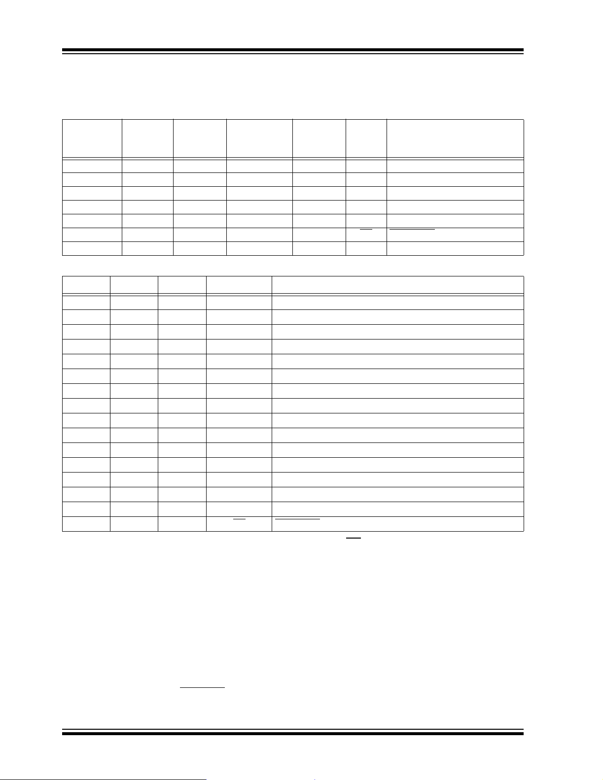
1.0 ELECTRICAL CHARACTERISTICS
† Notice: Stresses above those listed under “Maximum Rat-
ings” may cause permanent damage to the devic e. This is a
stress rating only and functional operation of the device at
those or any other conditions above those indicated in the
Absolute Maximum Ratings †
VDD – VSS........................................................................7.0V
All Inputs and Outputs ................... V
Difference Input Voltage ......................................|V
– 0.3V to VDD + 0.3V
SS
– VSS|
DD
operational listings of this specification is not implied. Exposure to maximum rating conditions for extended periods m ay
affect device reliability.
Output Short Circuit Current .................................Continuous
Current at Input Pins ....................................................±2 mA
Current at Output and Supply Pins ............................±30 mA
Storage Temperature.....................................-65°C to +150°C
Junction Temperature (T
) ..........................................+150°C
J
ESD Protection On All Pins (HBM;MM)................≥ 4 kV;400V
DC ELECTRICAL SPECIFICATIONS
Electrical Characteristics: Unless otherwise indicated, TA = +25°C, VDD = +2.2V to +5.5V, VSS = GND,
V
= VDD/2, RL = 10 kΩ to VDD/2 and V
CM
Parameters Sym Min Typ Max Units Conditions
Input Offset
Input Offset Voltage V
Input Offset Voltage
(Extended Temperat ure)
Input Offset Temperature Drift ∆V
Power Supply Rejection Ratio PSRR 70 90 — dB V
Input Bias, Input Offset Cur r e nt an d Im pe da nce
Input Bias Current I
At Temperature I
At Temperature I
Input Offset Current I
Common Mode Input Impedance Z
Differential Input Impedance Z
Common Mode (Note 4)
Common Mode Input Range V
Common Mode Rejection Ratio CMRR 70 85 — dB V
Common Mode Rejection Ratio CMRR 65 80 — dB V
Open-Loop Gain
DC Open-Loop Gain (Large Signal) A
Output
Maximum Output Voltage Swing V
Output Short Circuit Current I
Power Supply
Supply Voltage V
Quiescent Current per Amplifier I
Note 1: The MCP6285’s V
for op amp B (pins V
CM
2: The current at the MCP6285’s V
3: This specification does not apply to the MCP6285’s V
4: The MCP6285’s V
The MCP6285’s V
– pin (op amp B) has a c om m on mode range (V
INB
OUTA/VINB
≈ VDD/2.
OUT
OS
V
OS
/∆T
OS
B
B
B
OS
CM
DIFF
CMR
OL
, VOHV
OL
SC
DD
Q
– pin is specified by IB only.
INB
+ pin (op amp B) has a vo ltag e range specified by VOH and VOL.
-3.0 — +3.0 mV VCM = VSS (Note 1)
-5.0 — +5.0 mV TA= -40°C to +125°C,
V
CM
—±1.7—µV/°CT
A
= -40°C to +125°C,
A
V
CM
CM
— ±1.0 — pA Note 2
— 50 200 pA TA= +85°C (Note 2)
—2 5nAT
= +125°C (Note 2)
A
— ±1.0 — pA Note 3
—1013||6 — Ω||pF Note 3
—1013||3 — Ω||pF Note 3
V
− 0.3 — V
SS
90 110 — dB V
+ 15 — V
SS
+ 0.3 V
DD
– 15 mV
DD
CM
CM
OUT
V
CM=VSS
—±25—mA
2.2 — 5.5 V
300 450 570 µA IO = 0
OUTA/VINB
+ and V
OUTA/VINB
–) is VSS + 100 mV.
INB
+ pin.
) of VSS + 100 m V to VDD – 100 mV.
CMR
= V
(Note 1)
SS
= VSS (Note 1)
= VSS (Note 1)
= -0.3V to 2.5V, V
= -0.3V to 5.3V, V
DD
DD
= 0.2V to VDD – 0.2V,
(Note 1)
= 5V
= 5V
DS21811D-page 2 2004 Microchip Technology Inc.
MCP6281/2/3/4/5
AC ELECTRICAL SPECIFICATIONS
Electrical Characteristics: Unless otherwise indicated, TA = +25°C, VDD = +2.2V to +5.5V, VSS = GND,
V
= VDD/2, V
CM
AC Response
Gain Bandwidth Product GBWP — 5.0 — MHz
Phase Margin at Unity-Gain PM — 65 — °
Slew Rate SR — 2.5 — V/µs
Noise
Input Noise Voltage E
Input Noise Voltage Density e
Input Noise Current Density i
TEMPERATURE SPECIFICATIONS
Electrical Characteristics: Unless otherwise indicated, V
Temperature Ranges
Operating Temperature Range T
Storage Temperature Range T
Thermal Package Resistances
Thermal Resistance, 5L-SOT-23 θ
Thermal Resistance, 6L-SOT-23 θ
Thermal Resistance, 8L-PDIP θ
Thermal Resistance, 8L-SOIC θ
Thermal Resistance, 8L-MSOP θ
Thermal Resistance, 14L-PDIP
Thermal Resistance, 14L-SOIC
Thermal Resistance, 14L-TSSOP
Note: The Junction Temperature (T
≈ VDD/2, RL = 10 kΩ to VDD/2 and CL = 60 pF.
OUT
Parameters Sym Min Typ Max Units Conditions
ni
ni
ni
—3.5— µV
P-P
—16—nV/√Hz f = 1 kHz
—3—fA/√Hz f = 1 kHz
= +2.2V to +5.5V and VSS = GND.
DD
Parameters Sym Min Typ Max Units Conditions
A
A
JA
JA
JA
JA
JA
θ
JA
θ
JA
θ
JA
) must not exceed the Absolute Maximum specification of +150°C.
J
-40 — +125 °C Note
-65 — +150 °C
— 256 — °C/W
— 230 — °C/W
—85—°C/W
— 163 — °C/W
— 206 — °C/W
—
—
—
70
120
100
—
—
—
°C/W
°C/W
°C/W
f = 0.1 Hz to 10 Hz
2004 Microchip Technology Inc. DS21811D-page 3
MCP6281/2/3/4/5
.)
MCP6283/MCP6285 CHIP SELECT (CS) SPECIFICATIONS
Electrical Characteristics: Unless otherwise indicated, TA = +25°C, VDD = +2.2V to +5.5V, VSS = GND,
= VDD/2, V
V
CM
CS
Low Specifications
CS
Logic Threshold, Low V
Input Current, Low I
CS
CS High Specifications
CS
Logic Threshold, High V
Input Current, High I
CS
GND Current per Amplifier I
Amplifier Output Leakage — — 0.01 — µA CS = V
Dynamic Specifications (Note 1)
Low to Valid Amplifier
CS
Output, Turn-on Time
CS
High to Amplifier Output High-Z t
Hysteresis V
Note 1: The input condition (V
≈ VDD/2, RL = 10 kΩ to VDD/2 and CL = 60 pF.
OUT
Parameters Sym Min Typ Max Units Conditions
) specified applies to both op amp A and B of the MCP6285. The dynamic specification is tested
at the output of op amp B (V
IN
CSL
CSH
SS
t
ON
OFF
HYST
OUTB
IL
IH
V
SS
—0.01—µACS = V
0.8 V
DD
—0.7 2µACS = V
—-0.7—µACS = V
—410µsCS Low ≤ 0.2 VDD, G = +1 V/V,
—0.01—µsCS High ≥ 0.8 VDD, G = +1 V/V,
—0.6—VV
).
—0.2VDDV
—VDDV
V
= VDD/2, V
IN
= 5.0V
V
DD
= VDD/2, V
V
IN
= 5V
DD
SS
DD
DD
DD
= 0.9 VDD/2,
OUT
= 0.1 VDD/2
OUT
CS
V
I
SS
I
CS
OUT
Hi-Z
-0.7 µA (typ.)
0.7 µA (typ.)
V
IL
t
ON
-450 µA (typ.)
V
IH
t
OFF
Hi-Z
-0.7 µA (typ
0.7 µA (typ.)
10 nA (typ.)
FIGURE 1-1: Timing Diagram for the
C
hip Select (CS) pin on the MCP6283 and
MCP6285.
DS21811D-page 4 2004 Microchip Technology Inc.
MCP6281/2/3/4/5
2.0 TYPICAL PERFORMANCE CURVES
Note: The gr ap hs and tables provided following this note are a statistical summary based on a l im ite d n um ber of
samples and are prov ided for informational purposes only. The performance characteristics listed herein
are not tested or guaranteed. In some graphs or tables, the data presented may be outside the specified
operating range (e.g., outside specified power supply range) and therefore outside the warranted range.
Note: Unless otherwise indicated, TA = +25°C, VDD = +2.2V to +5.5V, VSS = GND, VCM = VDD/2, V
= 10 kΩ to VDD/2 and CL = 60 pF.
R
L
OUT
≈ VDD/2,
14%
832 Samples
= V
V
CM
SS
0.0
0.4
0.8
1.2
-2.8
-2.4
-2.0
-1.6
-1.2
-0.8
-0.4
1.6
Percentage of Occurrences
12%
10%
8%
6%
4%
2%
0%
Input Offset Voltage (mV)
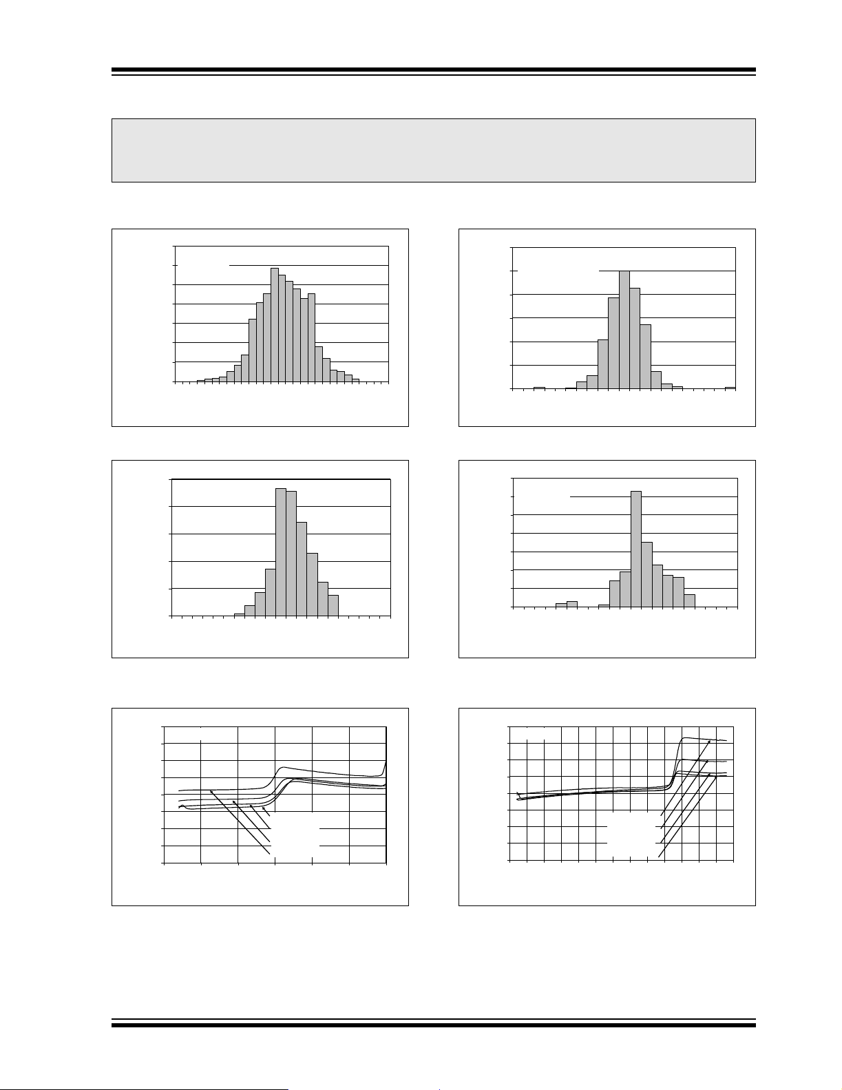
FIGURE 2-1: Input Offset Voltage.
25%
210 Samples
= +85°C
T
A
20%
15%
10%
5%
Percentage of Occurrences
0%
0 102030405060708090100
Input Bias Current (pA)
30%
832 Samples
= V
V
CM
25%
20%
15%
10%
5%
Percentage of Occurrences
2.0
2.4
2.8
0%
SS
TA = -40°C to +125°C
-10-8-6-4-2 0 2 4 6 810
Input Offset Voltage Drift (µV/°C)
FIGURE 2-4: Input Offset Voltage Drift.
35%
210 Samples
= +125°C
T
A
30%
25%
20%
15%
10%
5%
0%
Percentage of Occurrences
0
200
400
800
1200
1600
2000
2400
2800
3200
3600
Input Bias Current (pA)
FIGURE 2-2: Input Bias Cur rent at
=+85 °C.
T
A
300
VDD = 2.2V
250
200
150
100
50
0
-50
Input Offset Voltage (µV)
-100
-0.5 0.0 0.5 1.0 1.5 2.0 2.5
TA = +125°C
= +85°C
T
A
= +25°C
T
A
= -40°C
T
A
Common Mode Input Voltage (V)
FIGURE 2-3: Input Offset Voltage vs.
Common Mode Input Voltage at V
= 2.2V.
DD
FIGURE 2-5: Input Bias Current at
T
= +125 °C.
A
300
VDD = 5.5V
250
200
150
100
Input Offset Voltage (µV)
-50
-100
50
0
0.0
0.5
-0.5
1.0
1.5
TA = +125°C
= +85°C
T
A
= +25°C
T
A
= -40°C
T
A
2.0
2.5
3.0
3.5
4.0
4.5
5.0
Common Mode Input Voltage (V)
FIGURE 2-6: Input Offset Voltage vs.
Common Mode Input Voltage at V
= 5.5V.
DD
5.5
6.0
2004 Microchip Technology Inc. DS21811D-page 5
MCP6281/2/3/4/5
5
TYPICAL PERFORMANCE CURVES (CONTINUED)
Note: Unless otherwise indicated, TA = +25°C, VDD = +2.2V to +5.5V, VSS = GND, VCM = VDD/2, V
= 10 kΩ to VDD/2 and CL = 60 pF.
R
L
OUT
≈ VDD/2,
300
250
200
150
100
50
0
VDD = 2.2V
-50
Input Offset Voltage (µV)
-100
0.0 0.5 1.0 1.5 2.0 2.5 3.0 3.5 4.0 4.5 5.0 5.5
VCM = V
SS
Representative Part
VDD = 5.5V
Output Voltage (V)
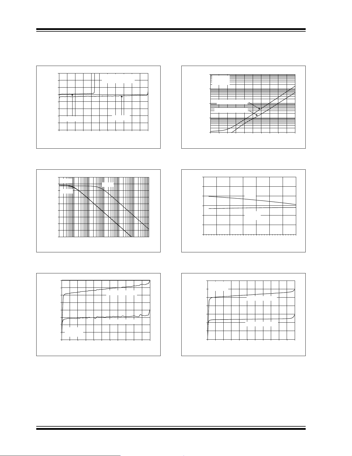
FIGURE 2-7: Input Offset Voltage vs. Output Voltage.
110
PSRR-
100
90
PSRR+
80
70
60
50
CMRR, PSRR (dB)
40
30
20
1.E+00 1.E+01 1.E+02 1.E+03 1.E+04 1.E+05 1.E+06
1 10k 100k 1M10010 1k
CMRR
Frequency (Hz)
10,000
VCM = V
DD
VDD = 5.5V
1,000
Input Bias Current
100
(pA)
Input Bias, Offset Currents
Input Offset Current
10
1
25 35 45 55 65 75 85 95 105 115 125
Ambient Temperature (°C)
FIGURE 2-10: Input Bias, Input Offset Currents vs. Ambient Temperature.
120
110
100
90
80
PSRR, CMRR (dB)
70
60
-50-250 25507510012
Ambient Temperature (°C)
CMRR
PSRR
V
CM
= V
SS
FIGURE 2-8: CMRR, PSRR vs. Frequency.
55
45
35
25
15
(pA)
5
-5
TA = +85°C
-15
V
Input Bias, Offset Currents
= 5.5V
DD
-25
0.0 0.5 1.0 1.5 2.0 2.5 3.0 3.5 4.0 4.5 5.0 5.5
Input Bias Current
Input Offset Curre nt
Common Mode Input Voltage (V)
FIGURE 2-9: Input Bias, Offset Currents
vs. Common Mode Input Voltage at T
=+85°C.
A
FIGURE 2-11: CMRR, PSRR vs. Ambient Temperature.
2.5
TA = +125°C
= 5.5V
V
DD
2.0
1.5
1.0
0.5
(nA)
0.0
-0.5
Input Bias, Offset Currents
-1.0
0.00.51.01.52.02.53.03.54.04.55.05.5
Input Bias Current
Input Offset Current
Common Mode Input Voltage (V)
FIGURE 2-12: Input Bias, Offset Currents vs. Common Mode Input Voltage at TA= +125°C.
DS21811D-page 6 2004 Microchip Technology Inc.

MCP6281/2/3/4/5
5.5
Maximum Output Voltage
Gain Bandwidth Product
Gain Bandwidth Product
Phase Margin
TYPICAL PERFORMANCE CURVES (CONTINUED)
Note: Unless otherwise indicated, TA = +25°C, VDD = +2.2V to +5.5V, VSS = GND, VCM = VDD/2, V
= 10 kΩ to VDD/2 and CL = 60 pF.
R
L
OUT
≈ VDD/2,
600
500
400
300
200
(µA/amplifier)
Quiescent Current
100
0
0.0 0.5 1.0 1.5 2.0 2.5 3.0 3.5 4.0 4.5 5.0
TA = +125°C
= +85°C
T
A
= +25°C
T
A
= -40°C
T
A
Power Supply Voltage (V)
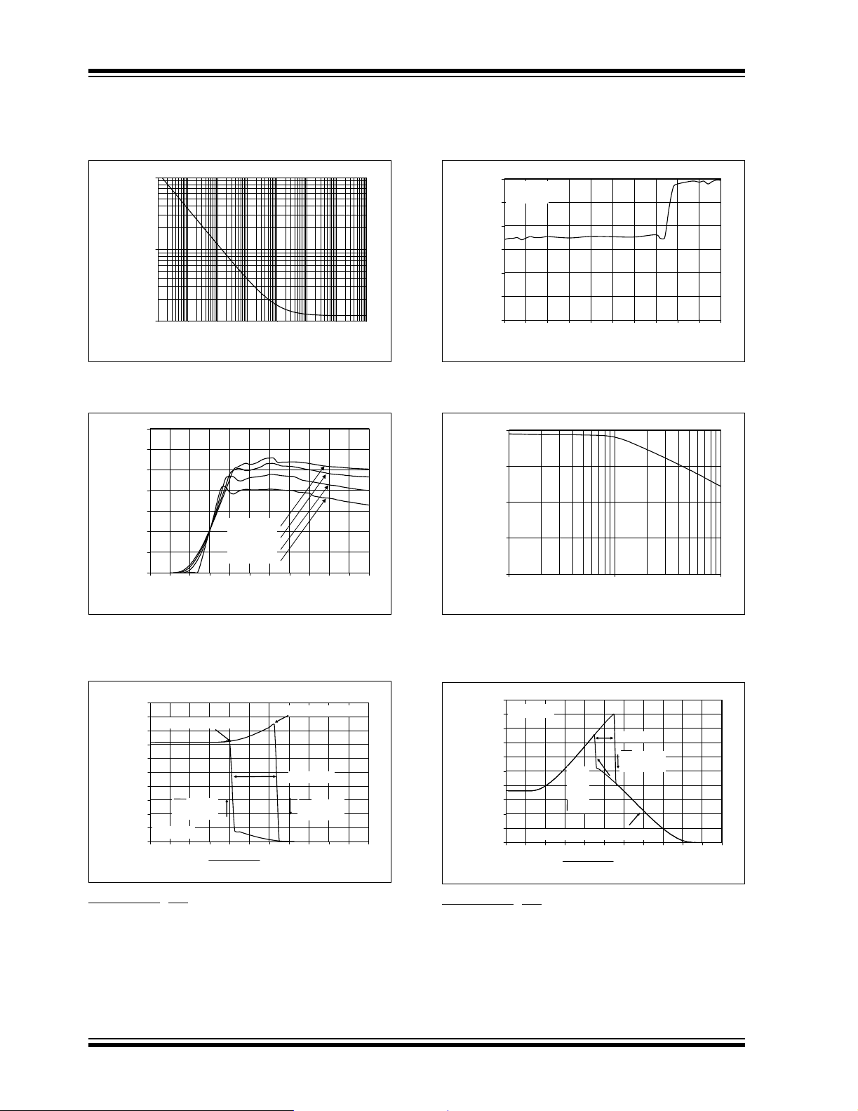
FIGURE 2-13: Quiescent Current vs. Power Supply Voltage.
120
100
80
60
40
20
Open-Loop Gain (dB)
0
-20
1.E-01
0.1
Phase
1.E+00
1.E+01
1 10 100 1k 10k 100k 1M 10M 100M
Gain
1.E+02
1.E+03
1.E+04
1.E+05
1.E+06
Frequency (Hz)
0
-30
-60
-90
-120
-150
-180
-210
1.E+07
1.E+08
Open-Loop Phase (°)
1000
100
10
1
Ouput Voltage Headroom (mV)
0.01 0.1 1 10
VOL - V
SS
VDD - V
OH
Output Current Magnitude (mA)
FIGURE 2-16: Output Voltage Headroom vs. Output Current Magnitude.
6
5
4
3
(MHz)
2
1
0
-50 -25 0 25 50 75 100 125
VDD = 2.2V
VDD = 5.5V
VDD = 2.2V
VDD = 5.5V
Ambient Temperature (°C)
90
85
80
75
70
65
60
Phase Margin (°)
FIGURE 2-14: Open-Loop Gain, Phase vs. Frequency.
10
VDD = 5.5V
)
P-P
VDD = 2.2V
1
Swing (V
0.1
1.E+03
1k 10k 100k 1M
1.E+04
1.E+05
1.E+06
10M
1.E+07
Frequency (Hz)
FIGURE 2-15: Maximum Output Voltage Swing vs. Frequency.
FIGURE 2-17: Gain Bandwidth Product, Phase Margin vs. Ambient Temperature.
4.5
4.0
Falling Edge, VDD = 5.5V
3.5
3.0
2.5
2.0
1.5
Slew Rate (V/µs)
1.0
0.5
0.0
-50 -25 0 25 50 75 100 125
Falling Edge, VDD = 2.2V
Rising Edge, VDD = 2.2V
Rising Edge, VDD = 5.5V
Ambient Temperature (°C)
FIGURE 2-18: S lew Rate vs . Ambi en t Temperature.
2004 Microchip Technology Inc. DS21811D-page 7
MCP6281/2/3/4/5
Ouptut Short Circuit Current
Quiescent Current
Channel-to-Channel Separation
Quiescent Current
TYPICAL PERFORMANCE CURVES (CONTINUED)
Note: Unless otherwise indicated, TA = +25°C, VDD = +2.2V to +5.5V, VSS = GND, VCM = VDD/2, V
= 10 kΩ to VDD/2 and CL = 60 pF.
R
L
OUT
≈ VDD/2,
1,000
Hz)
100
(nV/
Input Noise Voltage Density
10
1.E-01 1.E+00 1.E+01 1.E+02 1.E+03 1.E+04 1.E+05 1.E+06
0.1 10010 1k 100k10k 1M1
Frequency (Hz)
FIGURE 2-19: Input Noise Voltage Density vs. Frequency.
35
30
25
20
15
(mA)
10
5
0
0.0 0.5 1.0 1.5 2.0 2.5 3.0 3.5 4.0 4.5 5.0 5.5
TA = +125°C
T
= +85°C
A
T
= +25°C
A
= -40°C
T
A
Power Supply Voltage (V)
30
f = 1 kHz
= 5.0V
V
DD
25
20
15
(nV/¥Hz)
10
5
Input Noise Voltage Density
0
0.0 0.5 1.0 1.5 2.0 2.5 3.0 3.5 4.0 4.5 5.0
Common Mode Input Voltage (V)
FIGURE 2-22: Input Noise Voltage Density vs. Common Mode Input Voltage at 1 kHz.
140
130
120
(dB)
110
100
1 10 100
Frequency (kHz)
FIGURE 2-20: Output Short Circuit Current vs. Power Supply Voltage.
500
450
Op-Amp turns on here
400
350
300
250
200
150
(µA/Amplifier)
CS swept
high to low
100
50
VDD = 2.2V
0
0.00.20.40.60.81.01.21.41.61.82.02.2
Chip Select Voltage (V)
Op-Amp shuts off here
Hysteresis
CS swept
low to high
FIGURE 2-21: Quiescent Current vs.
hip Select (CS) Voltage at VDD = 2.2V
C
(MCP6283 and MCP6285 only).
FIGURE 2-23: Channel-to-Channel Separation vs. Frequency (MCP6282 and MCP6284 only).
1000
VDD = 5.5V
900
800
700
600
500
400
(µA/Amplifier)
300
200
100
0
0.00.51.01.52.02.53.03.54.04.55.05.5
CS swept
Op Amp toggles On/Off here
Hysteresis
CS swept
low to high
high to low
Chip Select Voltage (V)
FIGURE 2-24: Quiescent Current vs.
C
hip Select (CS) Voltage at VDD = 5.5V
(MCP6283 and MCP6285 only).
DS21811D-page 8 2004 Microchip Technology Inc.
MCP6281/2/3/4/5
Chip Select, Output Voltages
Chip Select, Output Voltages
TYPICAL PERFORMANCE CURVES (CONTINUED)
Note: Unless otherwise indicated, TA = +25°C, VDD = +2.2V to +5.5V, VSS = GND, VCM = VDD/2, V
= 10 kΩ to VDD/2 and CL = 60 pF.
R
L
OUT
≈ VDD/2,
5.0
4.5
4.0
3.5
3.0
2.5
2.0
1.5
Output Voltage (V)
1.0
0.5
0.0
0.E+00 2.E-06 4.E-06 6.E-06 8.E-06 1.E-05 1.E-05 1.E-05 2.E-05 2.E-05 2.E-05
G = +1V/V
V
= 5.0V
DD
Time (2 µs/div )
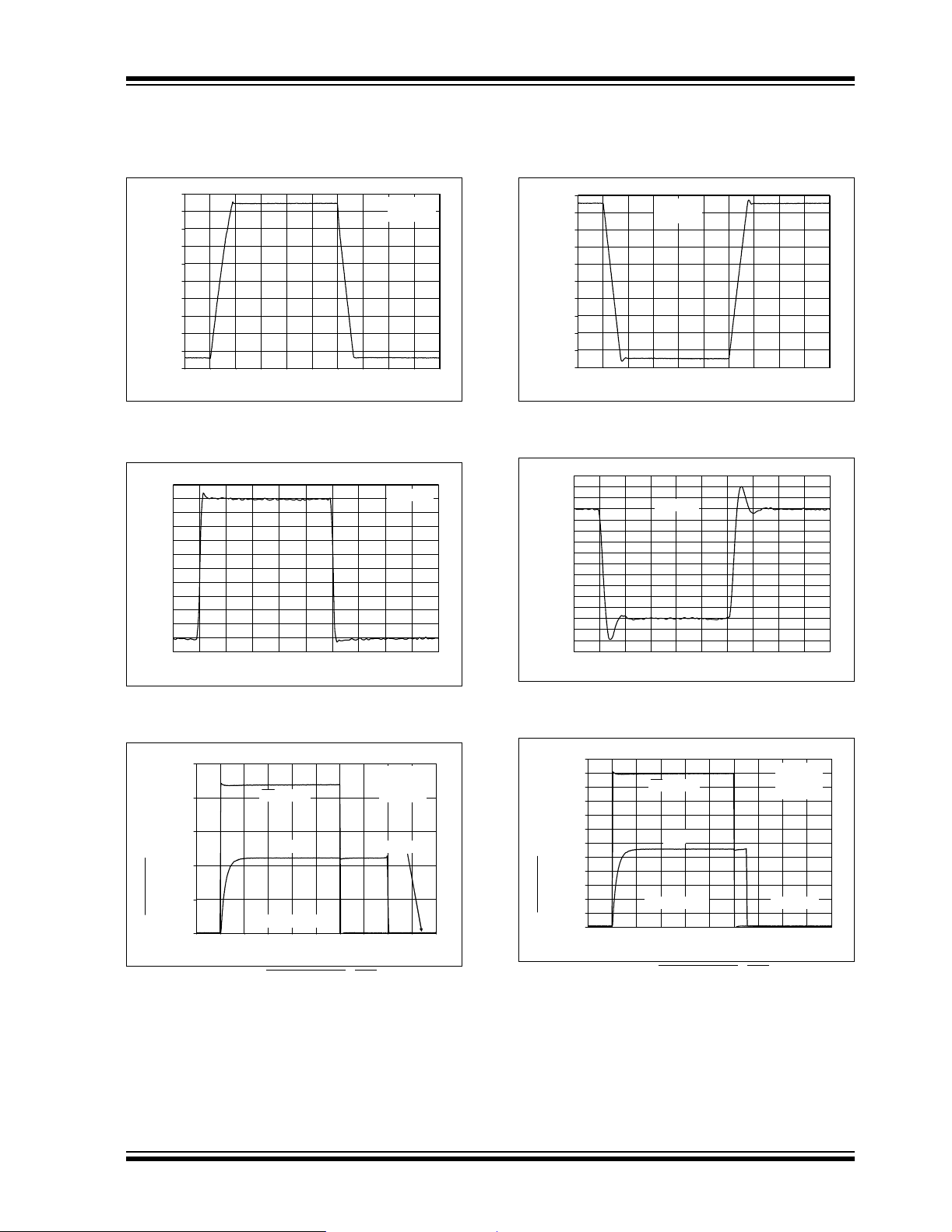
FIGURE 2-25: Large-Signal, Non-inverting Pulse Response.
G = +1V/V
Output Voltage (10 mV/div)
5.0
4.5
4.0
3.5
3.0
2.5
2.0
1.5
Output Voltage (V)
1.0
0.5
0.0
0.E+00 2.E-06 4.E-06 6.E-06 8.E-06 1.E-05 1.E-05 1.E-05 2.E-05 2.E-05 2.E-05
G = -1V/V
V
= 5.0V
DD
Time (2 µs/div)
FIGURE 2-28: Large-Signal, Inverting Pulse Response.
G = -1V/V
Output Voltage (10 mV/div)
Time (500 ns/div)
FIGURE 2-26: Sm all- Si gna l, Non-inverting Pulse Response.
2.5
2.0
1.5
(V)
1.0
0.5
0.0
0.0E+00 5.0 E-06 1. 0E-05 1. 5E-05 2. 0E-05 2 .5E-05 3.0E-05 3. 5E-05 4. 0E-05 4.5E -05 5 .0E-05
CS Voltage
V
OUT
Output High-Z
Time (5 µs/div)
FIGURE 2-27: C
hip Select (CS) to
Amplifier Output Response Time at V
VDD = 2.2V
G = +1V/V
V
= V
IN
Output On
= 2.2V
DD
SS
(MCP6283 and MCP6285 only).
Time (500 ns/div)
FIGURE 2-29: Sm al l- S ignal, Inverting Pulse Response.
6.0
5.5
5.0
4.5
4.0
3.5
3.0
(V)
2.5
2.0
1.5
1.0
0.5
0.0
0.E+00 5 .E-06 1 .E-05 2.E-05 2.E-05 3.E-05 3.E-05 4.E-05 4.E-05 5.E-05 5. E-05
CS Voltage
V
OUT
Time (5 µs/div)
FIGURE 2-30: C
hip Select (CS) to
Amplifier Output Response Time at V
VDD = 5.5V
G = +1V/V
V
= V
IN
Output OnOutput High-Z
= 5.5V
DD
SS
(MCP6283 and MCP6285 only).
2004 Microchip Technology Inc. DS21811D-page 9
MCP6281/2/3/4/5
3.0 PIN DESCRIPTIONS
Descriptions of the pins are listed in Table 3-1 (single op amps) and Table 3-2 (dual and quad op amps).
TABLE 3-1: PIN FUNCTION TABLE FOR SINGLE OP AMPS
MCP6281
(PDIP , SOIC,
MSOP)
MCP6281
(SOT-23-5)
MCP6271R
(SOT-23-5)
611 6 1V
244 2 4V
333 3 3V
752 7 6V
425 4 2V
——— 8 5CSChip Select
1,5,8 — — 1,5 — NC No Internal Connection
TABLE 3-2: PIN FUNCTION TABLE FOR DUAL AND QUAD OP AMPS
MCP6282 MCP6284 MCP6285 Symbol Description
MCP6283
(PDIP , SOIC,
MSOP)
MCP6283
(SOT-23-6)
Symbol Description
Analog Outp ut
OUT
– Inverting Input
IN
+ Non-inverting Input
IN
Positive Power Supply
DD
Negative Power Supply
SS
11—V
222V
333V
848 V
55—V
666V
777V
—8—V
—9—V
—10— V
4114 V
—12— V
—13— V
—14—V
—— 1V
OUTA
– Inverting Input (op amp A)
INA
+ Non-inverting Input (op amp A)
INA
DD
+ Non-inverting Input (op amp B)
INB
– Inverting Input (op amp B)
INB
OUTB
OUTC
– Inverting Input (op amp C)
INC
+ Non-inverting Input (op amp C)
INC
SS
+ Non-inverting Input (op amp D)
IND
– Inverting Input (op amp D)
IND
OUTD
OUTA/VINB
+ Analog Output (op amp A)/Non-inverting Input (op amp B)
—— 5 CS
3.1 Analog Outputs
The output pins are low-impedance voltage sources.
3.2 Analog Inputs
The non-inverting and inverting inputs are highimpedance CMOS inputs with low bias currents.
3.3 MCP6285’s V
OUTA/VINB
For the MCP6285 only, the output of op amp A is
connected directly to the non-inverting input of
op amp B; this is the V
OUTA/VINB
makes it possible to provide a Chip Select
in 8-pin packages.
+ Pin
+ pin. This connection
pin for duals
Analog Output (op amp A)
Positive Power Supply
Analog Output (op amp B)
Analog Output (op amp C)
Negative Power Supply
Analog Output (op amp D)
Chip Select
3.4 CS Digital Input
This is a CMOS, Schmitt-triggered input that places the
part into a low-power mode of operation.
3.5 Power Supply (VSS and VDD)
The positive powe r s upp ly (VDD) is 2.2V to 5.5V h igh er
than the negative power supply (V
operation, the other pins are between V
Typically, these parts are used in a single (positive)
supply configuration. In this case, V
ground and V
need a local bypass capacitor (typically 0.01 µF to
0.1 µF) within 2 mm of the V
to use a bulk capacitor (within 100 mm), which can be
shared with nearby analog parts.
DD
). For normal
SS
and VDD.
SS
is connected to
SS
is connected to the supply. VDD will
pin. These parts need
DD
DS21811D-page 10 2004 Microchip Technology Inc.

4.0 APPLICATION INFORMATION
MCP6281/2/3/4/5
The MCP6281/2/3/4/5 family of op amps is manufactured using Microchip's state-of-the-art CMOS
process. This family is specifically designed for lowcost, low-power and general purpose applications.
The low supply voltage, low quiescent current and
wide bandwidth makes the MCP6281/2/3/4/5 ideal for
battery-powered applications.
4.1 Rail-to-Rail Input s
The MCP6281/2/3/4/5 op amp is designed to prevent
phase reversal when the input pins exceed the supply
voltages. Fi gure 4-1 shows th e input vol tage exc eeding
the supply voltage without any phase reversal.
6
5
4
3
2
1
0
Input, Output Voltage (V)
-15 -14 -1 3 -12 -11 -10 -9 -8 -7 -6 -5
-1
V
IN
Time (1 ms/div)
V
OUT
FIGURE 4-1: The MCP6281/2/3/4/5 Show No Phase Reversal.
The input stage of the MCP6281/2/3/4/5 op amps use
two differential CMOS input stages in parallel. One
operates at low common mode input voltage (VCM),
while the other operates at high V
topology, the device operates with V
above V
age (V
V
DD
Input voltages that exceed the absolute maximum
voltage (V
excessive current to flow into or out of the input pins.
Current beyond ±2 mA can cause reliability problems.
Applications that exceed this rating must be externally
limited with a resistor, as shown in Figure 4-2.
and 0.3V below VSS. The Input Offset Volt-
DD
) is measured at VCM=VSS–0.3V and
OS
+ 0.3V to ensure proper operation.
– 0.3V to V
SS
+ 0.3V) can cause
DD
VDD = 5.0V
G = +2 V/V
. With this
CM
up to 0.3V
CM
–
IN
V
OUT
R
IN
V
IN
Maximum expected V
()VDD–
----------------------------------------------------------------------------------
R
≥
IN
V
SS
------------------------------------------------------------------------------
R
≥
IN
MCP628X
+
IN
2 mA
Minimum expected V
()–
2 mA
FIGURE 4-2: Input Current Limiting
Resistor (R
IN
).
4.2 Rail-to-Rail Output
The output voltage range of the MCP6281/2/3/4/5 op
amp is V
when R
V
= 5.5V. Refer to Figure 2-16 for more information.
DD
–15mV (min.) and VSS+15mV (max.)
DD
=10kΩ is connected to VDD/2 and
L
4.3 Capacitive Loads
Driving large capacitive loads can cause stability
problems for voltage feedback op amps. As the load
capacitance increases, the feedback loop’s phase
margin decreases and the closed-loop bandwidth is
reduced. This produces gain peaking in the frequency
response, with overshoot and ringing in the step
response. A unity-gain buffer (G = +1) is the most
sensitive to capa cit ive load s, th ough al l gain s show th e
same general behavior.
When driving large capacitive loads with these op
amps (e.g., > 100 pF when G = +1), a small series
resistor at the output (R
feedback loop’s phase margin (stability) by making the
output load resistive at higher frequencies. The
bandwidth will generally be lower than the bandwidth
with no capac itive load.
–
MCP628X
V
IN
+
in Figure 4-3) improves the
ISO
R
ISO
C
L
V
OUT
FIGURE 4-3: Output Resistor, R
ISO
stabiliz es large capacitive loads.
Figure 4-4 gives recommended R
ent capacitive loads and gains. The x-axis is the
normalized load capacitance (C
circuit's noise ga in. For non-inv erting gains, G
Signal Gain are equal. For inverting gains, G
1+|Signal Gain| (e.g., -1 V/V gives G
2004 Microchip Technology Inc. DS21811D-page 11
values for differ-
ISO
), where GN is the
L/GN
= +2 V/V).
N
and the
N
is
N

MCP6281/2/3/4/5
0
1,000
)
Ω
(
ISO
100
GN = 1 V/V
= 2 V/V
G
N
G
(CS)”.
≥ 4 V/V
N
ISO
's value until the
ISO
input, which can
Values
Recommended R
10
10 100 1,000 10,00
Normalized Load Capacitance; CL/GN (pF)
FIGURE 4-4: Recommended R
for Capacitive Loads.
After sele cting R
resulting frequency response peaking and step
response overshoot. Modify R
response is reasonable. Bench evaluation and simulations with the MCP6281/2/3/4/5 SPICE macro model
are helpful.
for your circuit, double-check the
ISO
4.4 MCP628X Chip Select (CS)
The MCP6283 and MCP6285 are single and dual op
amps with Chip Select
(CS), respectively. When CS is
pulled high, the sup ply current drops to 0.7 µA (typ) and
flows through the CS pin to VSS. When this happens,
the amplifier output is put into a high-impedance state.
By pulling CS
low, th e amplifier i s enabled. If the CS pin
is left floating, the amplifier may not operate properly.
Figure 1-1 shows the outp ut voltage and supply c urrent
response to a CS
pulse.
4.5 Cascaded Dual Op Amps
(MCP6285)
The MCP6285 is a dual op amp with Chip Select (CS).
The Chip Select
non-inverting input of a standard dual op amp (pin 5).
This pin is available because the output of op amp A
connects to the non-inverting input of op amp B, as
shown in Figure 4-5. The Chip Select
be connected to a microcontroller I/O line, puts the
device in Low-power mode. Refer to Section 4.4
“MCP6283/5 Chip Selec t
input is available on what would be the
V
OUTA/VINB
1
2
–
V
INA
A
INA
3
+
MCP6285
V
+
CS
V
INB
6
7
B
5
V
OUTB
–
FIGURE 4-5: Cascaded Gain Amplifier.
The output of op amp A is loaded by the input impedance of op amp B, which is typically 10
specified in the DC specification table (Refer to
Section 4.3 “Capacitive Loads” for further details
regarding capacitive loads).
The common mode input range of these op amps is
specified in the data sheet as V
+ 300 mV. However, since the output of op amp A
V
DD
is limite d to V
and VOH (20 mV from the rails with a
OL
10 kΩ load), the non-inverti ng in pu t range of op amp B
is limited to the common mode input range of
+ 20 mV and VDD–20mV.
V
SS
13
Ω||6pF, as
– 300 mV and
SS
4.6 Supply Bypass
With this family of operational amplifiers, the power
supply pin (V
for single-supply) should have a local
DD
bypass capacitor (i.e., 0.01 µF to 0.1 µF) within 2 mm
for good, high-frequency performance. It also needs a
bulk capaci tor (i.e., 1 µ F or larger) within 100 mm to
provide large, sl ow curre nts. T his bulk cap acitor ca n be
shared with other analog parts.
4.7 PCB Surface Leakage
In applications where low input bias current is critical,
Printed Circuit Board (PCB) surface-leakage effects
need to be considered. Surface leakage is caused by
humidity, dust or other contamination on the board.
Under low humidity conditions, a typical resistance
between nearby traces is 1 0
cause 5 pA of current to flow, which is greater than the
MCP6281/2/3/4/5 family’s bias current at 25°C (1pA,
typ.).
The easiest way to reduce surface leakage is to use a
guard ring around se nsi tiv e p ins (or t races). The guard
ring is biased at the same voltage as the sensitive pin.
An example of this type of layout is shown in
Figure 4-6.
12
Ω. A 5V dif ference would
DS21811D-page 12 2004 Microchip Technology Inc.

MCP6281/2/3/4/5
VIN–V
+
IN
V
SS
Guard Ring
FIGURE 4-6: Example Guard Ring Layout for Inverting Gain.
1. For Inverting Gain and Transimpedance
Amplifiers (convert current to voltage, such as
photo detectors):
a. Connect the guard ring to the non-inverting
input pin (V
to the same reference voltage as the op
amp (e.g., VDD/2 or ground).
b. Connect the inverting pin (VIN–) to the input
with a wire that does not touch the PCB
surface.
2. Non-inverting Gain and Unity-Gain Buffer:
a. Connect the non-inverting pin (V
input with a wire that does not touch the
PCB surface.
b. Connect the guard ring to the inverting input
pin (V
common mode i nput voltage.
+). This biases the guard ring
IN
+) to the
IN
–). This biases the g uard ri ng t o th e
IN
4.8 Application Circuits
4.8.1 SALLEN-KEY HIGH-PASS FILTER
The MCP6281/2/3/4/5 op amps can be used in activefilter applications. Figure 4-7 shows a second-order
Sallen-Ke y hi gh -pas s f il t er w i th a gai n o f 1 . The ou t pu t
bias voltage is set by the V
be changed to any voltage within the output voltage
range.
R
1
V
IN
C
C
1
2
R
2
VDD/2
FIGURE 4-7: Sallen-Key High-Pass Filter.
This filter, and others, can be designed using
Microchip’s FilterLab
our web site (www.microchip.com).
®
4.8.2 INVERTING MILLER INTEGRATOR
Analog integrators are used in filters, control loops an d
measurement circuits. Figure 4-8 shows the most
common implementation, the inverting Miller integrator.
The non-i nv ert i ng i n put i s at V
properly biases up. The sw itch (SW) is used to z ero the
output in some applications. Other applications use a
feedback loop to k eep the ou tpu t w it hin its linear range
of operation.
/2 reference, which can
DD
+
MCP6281
V
OUT
–
software, which is available on
/2 so that the op amp
DD
SW
RC
V
IN
V
OUT
+
MCP6281
VDD/2
–
V
OUT
V
IN
1
=
sRC
FIGURE 4-8: Miller Integrator.
2004 Microchip Technology Inc. DS21811D-page 13
MCP6281/2/3/4/5
T
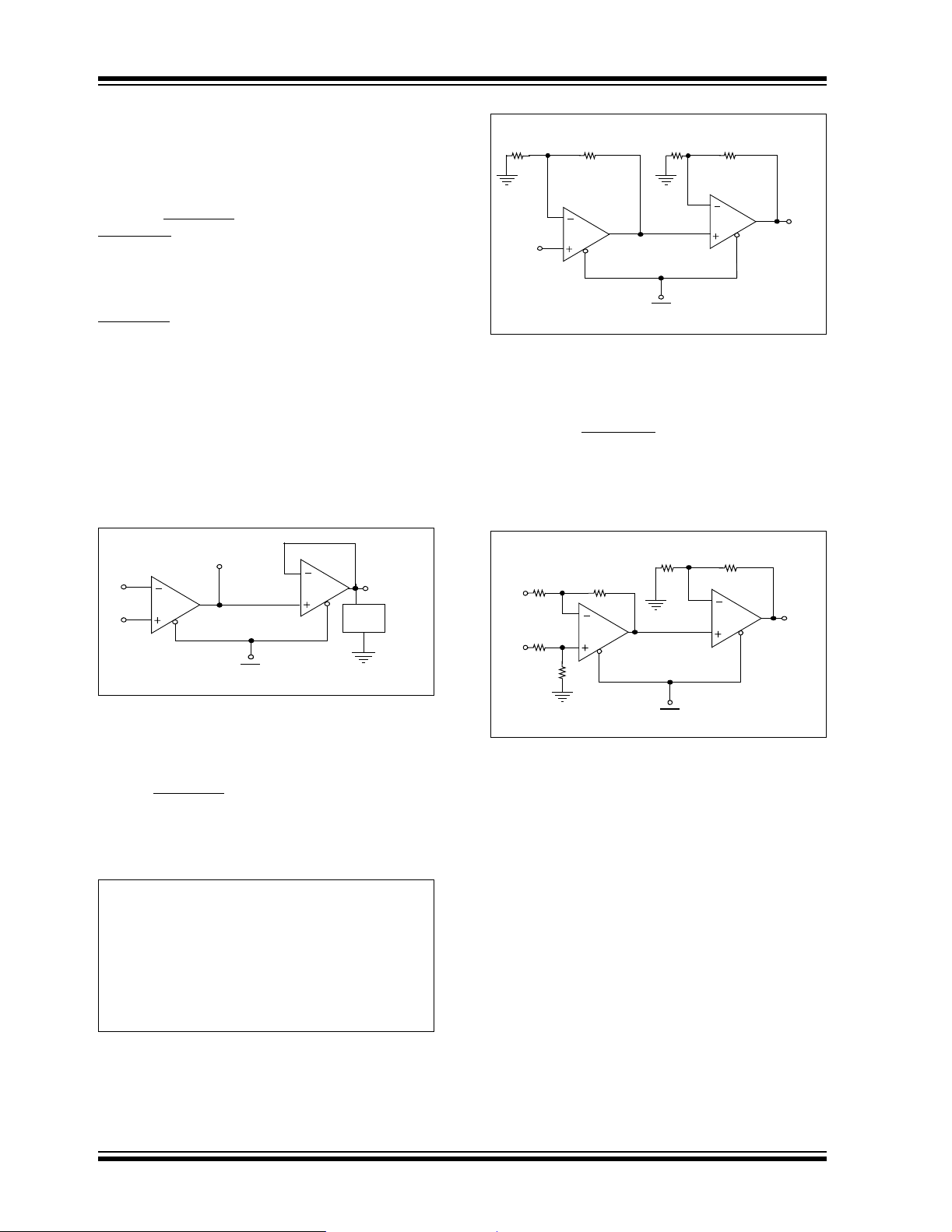
4.8.3 CASCADED OP AMP
APPLICATIONS
The MCP6285 provides the flexibility of Low-power
mode for dual op amps in an 8-pin package. The
MCP6285 eliminates the added cost and space in
battery-powered applications by using two single op
amps with Chip Select
hip Select line for both op amps. Since the two op
C
amps are internally cascaded, this device cannot be
used in circuits that require active or passive elements
between the two op amps. However, there are several
applications where this op amp configuration with
Select line becomes suitable. The circuits below
Chip
show possible applications for this device.
4.8.3.1 Load Isolation
With the cascaded op amp co nfiguration, op amp B can
be used to isolate the load from op amp A. In applications where op amp A is drivi ng cap aci tive o r low re sistance loads i n the feedbac k lo op (suc h as an integra tor
circuit or filter circuit), the op amp may not have
sufficient sou rce cu r re nt t o dri ve t he l oa d . In t h is case ,
op amp B can be used as a buffer.
lines or a 10-pi n device w ith one
R
4
V
IN
R
3
A
R
R
2
1
B
V
OU
MCP6285
CS
FIGURE 4-10: Cascaded Gain Circuit Configuration.
4.8.3.3 Difference Amplifier
Figure 4-1 1 shows op amp A c onfigured as a differe nce
amplifier with Chip Select
recommended to use well-matched resistors (e.g.,
0.1%) to increase the Common Mode Rejection Ratio
(CMRR). Op amp B can be used to provide additional
gain and isolate the load from the difference amplifier.
. In this configuration, it is
B
V
OUTB
A
MCP6285
Load
CS
FIGURE 4-9: Isolating the Load with a Buffer.
4.8.3.2 Cascaded Gain
Figure 4-10 shows a cascaded gain circuit configuration with Chip Select
in a non-inverting amplifier configuration. In this
configuration, i t is import ant to no te tha t t he in put of fs et
voltage of op amp A is amplified by the gain of
op amp A and B, as shown below:
V
OUTVINGAGBVOSAGAGBVOSBGB
Where:
= op amp A gain
G
A
G
= op amp B gain
B
= op amp A input offset voltage
V
OSA
= op amp B input offset voltage
V
OSB
. Op amps A and B are co nfi gure d
++=
R
4
R
2
V
IN2
R
V
2
IN1
R
R
1
A
MCP6285
1
R
3
B
V
OUT
CS
FIGURE 4-11: Difference Amplifier Circuit.
Therefore, it is recommended to set most of the gain
with op amp A and use op amp B with relatively small
gain (e.g., a unity-gain buffer).
DS21811D-page 14 2004 Microchip Technology Inc.
MCP6281/2/3/4/5
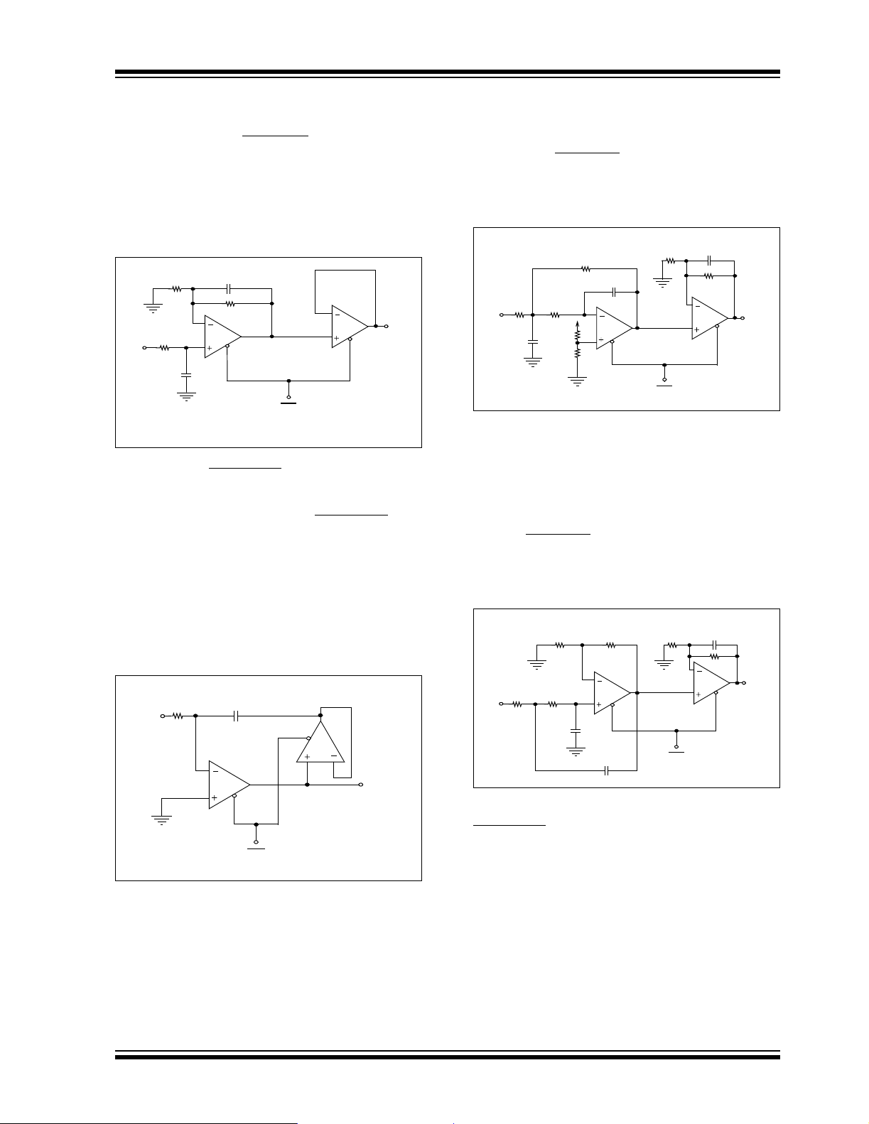
4.8.3.4 Buffered Non-inverting Integrator
Figure 4-12 shows a l oss y no n-in ve rtin g integrator that
is buffered and has a Chip Select
input. Op amp A is
configured as a non-inverting integrator. In this configuration, matching the impedance at each input is
recommended. R
at frequencies << 1/(2πR
is used to provide a feedback loop
F
) and makes this a lossy
1C1
integrator (it has a finit e gain at D C). Op am p B is use d
to isolate the load from the integrator.
R
2
R
V
1
IN
C
2
R
F
A
B
V
OUT
MCP6285
C
1
R
1C1
||
R2R
=
()C
F
CS
2
FIGURE 4-12: Buffered Non-inverting
Integrator with Chip Select
.
4.8.3.5 Inverting Integrator with Active
Compensation and C
Figure 4-13 uses an active compensator (op amp B) to
compensate for the non-ideal op amp characteristics
introduced at higher frequencies. This circuit uses
op amp B as a unity-gain buffer to isolate the integration
capacitor C1 from op amp A and drives the capacitor
with low-impedance source. Since both op amps are
matched very well, they provide a higher quality
integrator.
R
1
V
IN
C
1
hip Select
B
4.8.3.6 Second-Order MFB Low-Pass Filter
with an Extra Pole-Zero Pair
Figure 4-14 is a second-order multiple feedback lowpass filter with Chip Selec t
. Use the FilterLab® software
from Microchip to det ermine the R and C va lues for the
op amp A’s second-order filter. Op amp B can be used
1
A
, R6 and R7.
3
R
6
MCP6285
CS
C
3
R
7
V
B
OUT
to add a pole-zero pair using C
R
1
C
R
R
3
V
IN
C
2
R
2
5
R
4
FIGURE 4-14: Second-Order Multiple Feedback Low-Pass Filter with an Extra Pole-Zero Pair.
4.8.3.7 Second-Order Sallen-Key Low-Pass
Filter with an Extra Pole-Zero Pair
Figure 4-15 is a second-order Sallen-Key low-pass
filter with Chip Select
Microchip to determine the R and C values for the op
amp A’s second-order filter. Op amp B can be used to
add a pole-zero pair using C
R4R
V
IN
. Use the FilterLab® software from
, R5 and R6.
3
R
2
3
C
R
1
A
R
5
MCP6285
1
C
2
CS
C
3
R
6
V
B
OUT
A
MCP6285
V
OUT
FIGURE 4-15: Second-Order Sallen-Key
Low-Pass Filter with an Extra Pole-Zero Pair and
C
hip Select.
CS
FIGURE 4-13: Integrator Circuit with Active Compensation.
2004 Microchip Technology Inc. DS21811D-page 15

MCP6281/2/3/4/5
4.8.3.8 Capacitorless Second-Order
Low-Pass filter with Chip Select
The low-pass filter shown in Figure 4-16 does not
require external capacitors and uses only three external resistors; the op amp's GBWP sets the corner
frequency. R
and R
3
the frequency response, Q needs to be low (lower
values need to be selected for R3). Note that the amplifier bandwidth varies greatly over temperature and
process. However, this configuration provides a lowcost solution for applications with high bandwidth
requirements.
V
IN
V
REF
and R2 are used to set the circuit gain
1
is used to set the Q. To avoid gain peaking in
R
2
R
3
A
MCP6285
CS
R
1
B
V
OUT
FIGURE 4-16: Capacitorless Second-Order
Low-Pass Filter with Chip Select
.
5.0 DESIGN TOOLS
Microchip provides the basic design tools needed for
the MCP6281/2/3/4/5 family of op amps.
5.1 SPICE Macro Model
The latest SPICE macro model for the
MCP6281/2/3/4/5 op am ps is available on our web site
at www .microc hip.com. T his mod el is intended to be a n
initial design tool that works well in the op amp’s linear
region of operation at room temperature. See the
macro model file for information on its capabilities .
Bench testing is a very im portant part of any design an d
cannot be replaced with simulations. Also, simulation
results using this mac ro m od el ne ed to be v ali dated by
comparing them to the data sheet specifications and
characteristic curves.
5.2 FilterLab® Software
Microchip’s FilterLab software is an innova tive too l that
simplifies analog active-filter (usi ng op amps) design.
Available at no cost from our web site at
www.microchip.com, the FilterLab design tool provides
full schematic diagram s of the filte r circuit with component values. It also outpu ts th e filter circuit in SPICE
format, which can be used with the macro model to
simulate actual filter performance.
DS21811D-page 16 2004 Microchip Technology Inc.

6.0 PACKAGING INFORMATION
6.1 Package Marking Information
5-Lead SOT-23 (MCP6281 and MCP6281R)
Device Code
XXNN CH25
MCP6281 CHNN
MCP6281R EUNN
Note: Applies to 5-Lead SOT-23.
MCP6281/2/3/4/5
Example:
6-Lead SOT-23 (MCP6283)
Example:
XXNN CL25
8-Lead MSOP
XXXXXX
YWWNNN
8-Lead PDIP (300 mil)
XXXXXXXX
XXXXXNNN
YYWW
8-Lead SOIC (150 mil)
Example:
Example:
Example:
6281E
437256
MCP6281
E/P256
0437
XXXXXXXX
XXXXYYWW
NNN
Legend: XX...X Customer specific information*
YY Year code (last 2 digits of calendar year)
WW Week code (week of January 1 is week ‘01’)
NNN Alphanumeric traceability code
Note: In the event the full Micro chip p ar t number can not be marke d on one li ne, it wi ll
be carried over to the next line thus lim iti ng th e nu mb er of av ai lab le c hara ct ers
for customer specific information.
* Standard marking consists of Microchip part number, year code, week code, traceability code (facility
code, mask rev#, and assembly code). For marking beyond this, certain price adders apply. Please
check with your Microchip Sales Office.
2004 Microchip Technology Inc. DS21811D-page 17
MCP6281
E/SN0437
256

MCP6281/2/3/4/5
Package Marking Information (Continued)
14-Lead PDIP (300 mil) (MCP6284) Example:
XXXXXXXXXXXXXX
XXXXXXXXXXXXXX
YYWWNNN
14-Lead SO IC (150 mil) (MCP6284)
XXXXXXXXXX
XXXXXXXXXX
YYWWNNN
14-Lead TSSOP (MCP6284)
XXXXXX
YYWW
NNN
MCP6284-E/P
0437256
Example:
MCP6284ESL
0437256
Example:
6284EST
0437
256
DS21811D-page 18 2004 Microchip Technology Inc.

5-Lead Plastic Small Outline Transistor (OT) (SOT-23)
E
E1
p
B
p1
D
MCP6281/2/3/4/5
n
c
β
Number of Pins
Pitch
Outside lead pitch (basic)
Foot Angle
Lead Thickness
Mold Draft Angle Top
Mold Draft Angle Bottom
*Controlling Parameter
Notes:
Dimensions D and E1 do not include mold flash or protrusions. Mold flash or protrusions shall not
exceed .005" (0.127mm) per side.
1
A
φ
L
n
p
p1
φ
c
α
β
A1
α
A2
MILLIMETERSINCHES*Units
MAXNOMMINMAXNOMMINDimension Limits
55
0.95.038
1.90.075
1.451.180.90.057.046.035AOverall Height
1.301.100.90.051.043.035A2Molded Package Thickness
0.150.080.00.006.003.000A1Standoff
3.002.802.60.118.110.102EOverall Width
1.751.631.50.069.064.059E1Molded Package Width
3.102.952.80.122.116.110DOverall Length
0.550.450.35.022.018.014LFoot Length
10501050
0.200.150.09.008.006.004
0.500.430.35.020.017.014BLead Width
10501050
10501050
EIAJ Equivalent: SC-74A
Drawing No. C04-091
2004 Microchip Technology Inc. DS21811D-page 19

MCP6281/2/3/4/5
6-Lead Plastic Small Outline Transistor (CH) (SOT-23)
E
E1
B
n
c
β
Number of Pins
Pitch
Outside lead pitch (basic)
Molded Package Thickness
Standoff
Molded Package Width
Foot Angle
Lead Thickness
Mold Draft Angle Top
Mold Draft Angle Bottom
*Controlling Parameter
Notes:
Dimensions D and E1 do not include mold flash or protrusions. Mold flash or protrusions shall not
exceed .005" (0.127mm) per side.
n
p
p1
A2
A1
E1
φ
c
α
β
p1
D
1
A
φ
NOM
A1
MINMAX
L
MINDimension Limits
α
A2
MILLIMETERSINCHES*Units
NOM
66
MAX
0.95.038
1.90.075
1.451.180.90.057.046.035AOverall Height
1.301.100.90.051.043.035
0.150.080.00.006.003.000
3.002.802.60.118.110.102EOverall Width
1.751.631.50.069.064.059
3.102.952.80.122.116.110DOverall Length
0.550.450.35.022.018.014LFoot Length
10501050
0.200.150.09.008.006.004
0.500.430.35.020.017.014BLead Width
10501050
10501050
JEITA (formerly EIAJ) equivalent: SC-74A
Drawing No. C04-120
DS21811D-page 20 2004 Microchip Technology Inc.

8-Lead Plastic Micro Small Outline Package (MS) (MSOP)
E
E1
p
D
B
n 1
2
MCP6281/2/3/4/5
α
L
.033
.006
.012
A
φ
A1
MAX NOM
8
--
.043
.037
.006
-
.009
.016
-
-
MIN
.031
15°
15°
0.75
0.00
0.40
0.08
0.22
c
(F)
β
Dimension Limits
Units
Number of Pins
Pitch
Overall Height
Molded Package Thickness
Standoff
Overall Width
Molded Package Width
Overall Length
Foot Length
Foot Angle
Lead Thickness
Lead Width
Mold Draft Angle Top
Mold Draft Angle Bottom
*Controlling Parameter
Notes:
Dimensions D and E1 do not include mold flash or protrusions. Mold flash or protrusions shall not
exceed .010" (0.254mm) per side.
JEDEC Equivalent: MO-187
Drawing No. C04-111
MIN
n
p
A
A2
A1
E
E1
D
L
φ
c
B
α
β
INCHES
NOM
.026 BSC
.030
.000
.193 TYP.
.118 BSC
.118 BSC
.016 .024
.037 REFFFootprint (Reference)
0° - 8°
.003
.009
5°
5°
5° -
5° -
MILLIMETERS*
0.65 BSC
--
4.90 BSC
3.00 BSC
3.00 BSC
0.95 REF
0°
MAX
8
0.85
-
0.60
-
-
-
A2
1.10
0.95
0.15
0.80
8°
0.23
0.40
15°5° 15°5° -
2004 Microchip Technology Inc. DS21811D-page 21

MCP6281/2/3/4/5
8-Lead Plastic Dual In-line (P) – 300 mil (PDIP)
E1
D
2
n
E
β
eB
Number of Pins
Pitch
Top to Seating Plane A .140 .155 .170 3.56 3.94 4.32
Molded Package Thickness A2 .115 .130 .145 2.92 3.30 3.68
Base to Seating Plane A1 .015 0.38
Shoulder to Shoulder Width E .300 .313 .325 7.62 7.94 8.26
Molded Package Width E1 .240 .250 .260 6.10 6.35 6.60
Overall Length D .360 .373 .385 9.14 9.46 9.78
Tip to Seating Plane L .125 .130 .135 3.18 3.30 3.43
Lead Thickness
Upper Lead Width B1 .045 .058 .070 1.14 1.46 1.78
Lower Lead Width B .014 .018 .022 0.36 0.46 0.56
Overall Row Spacing § eB .310 .370 .430 7.87 9.40 10.92
Mold Draft Angle Top
Mold Draft Angle Bottom
* Controlling Parameter
§ Significant Characteristic
Notes:
Dimensions D and E1 do not include mold flash or protrusions. Mold flash or protrusions shall not exceed
.010” (0.254mm) per side.
JEDEC Equivalent: MS-001
Drawing No. C04-018
Dimension L imits MIN NOM MAX MIN NOM MAX
1
α
A
c
Units INCHES* MILLIMETERS
n
p
c
α
β
.008 .012 .015 0.20 0.29 0.38
A1
B1
B
88
.100 2.54
51015 51015
51015 51015
A2
L
p
DS21811D-page 22 2004 Microchip Technology Inc.

8-Lead Plastic Small Outline (SN) – Narrow, 150 mil (SOIC)
E
E1
p
D
2
MCP6281/2/3/4/5
B
Number of Pins
Pitch
Foot Angle
Lead Thickness
Mold Draft Angle Top
Mold Draft Angle Bottom
* Controlling Parameter
§ Significant Characteristic
Notes:
Dimensions D and E1 do not include mold flash or protrusions. Mold flash or protrusions shall not exceed
.010” (0.254mm) per side.
JEDEC Equivalent: MS-012
Drawing No. C04-057
n
45°
c
β
n
p
φ
c
α
β
1
h
A
φ
L
048048
A1
MILLIMETERSINCHES*Units
1.27.050
α
A2
MAXNOMMINMAXNOMMINDimension Limits
88
1.751.551.35.069.061.053AOverall Height
1.551.421.32.061.056.052A2Molded Package Thickness
0.250.180.10.010.007.004A1Standoff §
6.206.025.79.244.237.228EOverall Width
3.993.913.71.157.154.146E1Molded Package Width
5.004.904.80.197.193.189DOverall Length
0.510.380.25.020.015.010hChamfer Distance
0.760.620.48.030.025.019LFoot Length
0.250.230.20.010.009.008
0.510.420.33.020.017.013BLead Width
1512015120
1512015120
2004 Microchip Technology Inc. DS21811D-page 23

MCP6281/2/3/4/5
14-Lead Plastic Dual In-line (P) – 300 mil (PDIP)
E1
D
2
n
E
β
eB
Number of Pi ns
Pitch
Top to Seating Plane A .140 .155 .170 3.56 3.94 4.32
Molded Package Thickness A2 .115 .130 .145 2.92 3.30 3.68
Base to Seating Plane A1 .015 0.38
Shoulder to Shoulder Width E .300 .313 .325 7.62 7.94 8.26
Molded Package Width
Overall Length D .740 .750 .760 18.80 19.05 19.30
Tip to Seating Plane L .125 .130 .135 3.18 3.30 3.43
Lead Thickness
Upper Lead Width B1 .045 .058 .070 1.14 1.46 1.78
Lower Lead Width B .014 .018 .022 0.36 0.46 0.56
Overall Row Spacing § eB .310 .370 .430 7.87 9.40 10.92
Mold Draft Angle Top
Mold Draft Angle Bottom
* Controlling Parameter
§ Significant Characteristic
Notes:
Dimensions D and E1 do not include mold flash or protrusions. Mold flash or protrusions shall not exceed
.010” (0.254mm) per side.
JEDEC Equivalent: MS-001
Drawing No. C04-005
1
A
c
A1
Dimension Limits MIN NOM MAX MIN NOM MAX
Units INCHES* MILLIMETERS
n
p
E1
c
α
β
.240 .250 .260 6.10 6.35 6.60
.008 .012 .015 0.20 0.29 0.38
5 10 15 5 10 15
5 10 15 5 10 15
B1
B
14 14
.100 2.54
α
A2
L
p
DS21811D-page 24 2004 Microchip Technology Inc.

MCP6281/2/3/4/5
14-Lead Plastic Small Outline (SL) – Narrow, 150 mil (SOIC)
E
E1
p
D
2
B
n
1
45°
c
β
Number of Pins
Pitch
Foot Angle
Lead Thickne ss
Mold Draft Angle Top
Mold Draft Angle Bottom
* Controlling Parameter
§ Significant Characteristic
Notes:
Dimensions D and E1 do not include mold flash or protrusions. Mold flash or protrusions shall not exceed
.010” (0.254mm) per side.
JEDEC Equivalent: MS-012
Drawing No. C04-065
h
A
φ
L
n
p
φ
c
α
β
A1
048048
α
MILLIMETERSINCHES*Units
1.27.050
A2
MAXNOMMINMAXNOMMINDimension Limits
1414
1.751.551.35.069.061.053AOverall Height
1.551.421.32.061.056.052A2Molded Package Thick ness
0.250.180.10.010.007.004A1Standoff §
6.205.995.79.244.236.228EOverall Width
3.993.903.81.157.154.150E1Molded Package Width
8.818.698.56.347.342.337DOverall Length
0.510.380.25.020.015.010hChamfer Distance
1.270.840.41.050.033.016LFoot Length
0.250.230.20.010.009.008
0.510.420.36.020.017.014BLead Width
1512015120
1512015120
2004 Microchip Technology Inc. DS21811D-page 25

MCP6281/2/3/4/5
14-Lead Plastic Thin Shrink Small Outline (ST) – 4.4 mm (TSSOP)
E
E1
p
D
2
n
B
1
A
c
φ
β
Number of Pins
Pitch
Foot Angle
Lead Thickne ss
Mold Draft Angle Top
Mold Draft Angle Bottom
* Controlling Parameter
§ Significant Characteristic
Notes:
Dimensions D and E1 do not include mold flash or protrusions. Mold flash or protrusions shall not exceed
.005” (0.127mm) per side.
JEDEC Equivalent: MO-153
Drawing No. C04-087
n
p
φ
c
α
β
L
MILLIMETERS*INCHESUnits
0.65.026
α
A2A1
MAXNOMMINMAXNOMMINDimension Limits
1414
1.10.043AOverall Height
0.950.900.85.037.035.033A2Molded Package Thickness
0.150.100.05.006.004.002A1Standoff §
6.506.386.25.256.251.246EOverall Width
4.504.404.30.177.173.169E1M old ed Pa ckag e Width
5.105.004.90.201.197.193DMolded Package Length
0.700.600.50.028.024.020LFoot Length
840840
0.200.150.09.008.006.004
0.300.250.19.012.010.007B1Lead Width
10501050
10501050
DS21811D-page 26 2004 Microchip Technology Inc.

APPENDIX A: REVISION HISTORY
Revision A (June 2003)
Original data sheet release.
Revision B (October 2003)
Revision C (June 2004)
Revision D (December 2004)
The following is the list of modifications:
1. Added SOT-23-5 packages for the MCP6281
and MCP6281R single op amps.
2. Added SOT-23-6 package for the MCP6283
single op amp.
3. Added Section 3.0 “Pin Descriptions”.
4. Corrected application circuits
(Section 4.8 “Application Circuits”).
5. Added SOT-23-5 and SOT-23-6 packages and
corrected package marking information
(Section 6.0 “Packaging Information”).
6. Added Appendix A: Revision History.
MCP6281/2/3/4/5
2004 Microchip Technology Inc. DS21811D-page 27

MCP6281/2/3/4/5
NOTES:
DS21811D-page 28 2004 Microchip Technology Inc.
MCP6281/2/3/4/5
PRODUCT IDENTIFICATION SYSTEM
To order or obtain information, e.g., on pricing or delivery, refer to the factory or the listed sales office.
PART NO. X /XX
Device
–
PackageTemperature
Range
Device: MCP6281: Single Op Amp
Temperature Range: E = -40°C to +125°C
Package: OT = Plastic Small Outline Transistor (SOT-23), 5-lead
MCP6281T: Single Op Amp
MCP6281RT: Single Op Amp
MCP6282: Dual Op Amp
MCP6282T: Dual Op Amp
MCP6283: Single Op Amp with Chip Select
MCP6283T: Single Op Amp with Chip Select
MCP6284: Quad Op Amp
MCP6284T: Quad Op Amp
MCP6285: Dual Op Amp with Chip Select
MCP6285T: Dual Op Amp with Chip Select
CH = Plastic Small Outline Transistor (SOT-23), 6-lead
MS = Plastic MSOP, 8-lead
P = Plastic DIP (300 mil Body), 8-lead, 14-lead
SN = Plastic SOIC, (150 mil Body), 8-lead
SL = Plastic SOIC (150 mil Body), 14-lead
ST = Plastic TSSOP (4.4mm Body), 14-lead
(Tape and Reel)
(SOIC, MSOP, SOT-23-5)
(Tape and Reel) (SOT-23-5)
(Tape and Reel) (SOIC, MSOP)
(Tape and Reel)
(SOIC, MSOP, SOT-23-6)
(Tape and Reel) (SOIC, TSSOP)
(Tape and Reel) (SOIC, MSOP)
(MCP6281, MCP6281R only)
(MCP6283 only)
Examples:
a) MCP6281-E/SN: Extended Temperature,
b) MCP6281-E/MS: Extended Temperature,
c) MCP6281-E/P: Extended Temperature,
d) MCP6281T-E/OT: Tape and Reel,
a) MCP6282-E/SN: Extended Temperature,
b) MCP6282-E/MS: Extended Temperature,
c) MCP6282-E/P: Extended Temperature,
d) MCP6282T-E/SN: Tape and Reel,
a) MCP6283-E/SN: Extended Temperature,
b) MCP6283-E/MS: Extended Temperature,
c) MCP6283-E/P: Extended Temperature,
d) MCP6283T-E/CH: Tape and Reel,
a) MCP6284-E/P: Extended Temperature,
b) MCP6284T-E/SL: Tape and Reel,
c) MCP6284-E/SL: Extended Temperature,
d) MCP6284-E/ST: Extended Temperature,
a) MCP6285-E/SN: Extended Temperature,
b) MCP6285-E/MS: Extended Temperature,
c) MCP6285-E/P: Extended Temperature,
d) MCP6285T-E/SN: Tape and Reel,
8LD SOIC package.
8LD MSOP package.
8LD PDIP package.
Extended Temperature,
5LD SOT-23 package.
8LD SOIC package.
8LD MSOP package.
8LD PDIP package.
Extended Temperature,
8LD SOIC package.
8LD SOIC package.
8LD MSOP package.
8LD PDIP package.
Extended Temperature,
6LD SOT-23 package.
14LD PDIP package.
Extended Temperature,
14LD SOIC package.
14LD SOIC package.
14LD TSSOP package.
8LD SOIC package.
8LD MSOP package.
8LD PDIP package.
Extended Temperature,
8LD SOIC package.
Sales and Support
Data Sheets
Products supported by a preliminary Data Sheet may have an errata sheet describing minor operational differences and
recommended workarounds. To determine if an errata sheet exists for a particular device, please contact one of the following:
1. Your local Microchip sales office
2. The Microchip Worldwide Site (www.microchip.com)
Please specify which device, revision of silicon and Data Sheet (include Literature #) you are using.
Customer Notification System
Register on our web site (www.microchip.com) to receive the most current information on our products.
2004 Microchip Technology Inc. DS21811D-page 29

MCP6281/2/3/4/5
NOTES:
DS21811D-page 30 2004 Microchip Technology Inc.

Note the following details of the code protection feature on Microchip devices:
• Microchip products meet the specification contained in their particular Microchip Data Sheet.
• Microchip believes that its family of products is one of the most secure families of its kind on the market today, when used in the
intended manner and under normal conditions.
• There are dishonest and possibly illegal methods used to breach the code protection feature. All of these methods, to our
knowledge, require using the Microchip products in a manner outside the operating specifications contained in Microchip’s Data
Sheets. Most likely, the person doing so is engaged in theft of intellectual property.
• Microchip is willing to work with the customer who is concerned about the integrity of their code.
• Neither Microchip nor any other semiconductor manufacturer can guarantee the security of their code. Code protection does not
mean that we are guaranteeing the product as “unbreakable.”
Code protection is constantly evolving. We at Microchip are committed to continuously improving the code protection features of our
products. Attempts to break Microchip’s code protection feature may be a violation of the Digital Millennium Copyright Act. If such acts
allow unauthorized access to your software or other copyrighted work, you may have a right to sue for relief under that Act.
Information contained in this publication regarding device
applications and the like is provided only for your convenience
and may be superseded by updates. It is your responsibility to
ensure that your application meets with your specifications.
MICROCHIP MAKES NO REPRESENTATIONS OR WARRANTIES OF ANY KIND WHETHER EXPRESS OR IMPLIED,
WRITTEN OR ORAL, STATUTORY OR OTHERWISE,
RELATED TO THE INFORMATION, INCLUDING BUT NOT
LIMITED TO ITS CONDITION, QUALITY, PERFORMANCE,
MERCHANTABILITY OR FITNESS FOR PURPOSE.
Microchip disclaims all liability arising from this information and
its use. Use of M icrochip’s produ cts as critical c omponents in
life support systems is not authorized except with express
written approval by Microchip. No licenses are conveyed,
implicitly or otherwise, under any Microchip intellectual property
rights.
Trademarks
The Microchip name and logo, the Microchip logo, Accuron,
dsPIC, K
EELOQ, microID, MPLAB, PIC, PICmicro, PICSTART ,
PRO MAT E, PowerSmart, rfPIC, and SmartShunt are
registered trademarks of Microchip Technology Incorporated
in the U.S.A. and other countries.
AmpLab, FilterLab, Migratable Memory, MXDEV, MXLAB,
PICMASTER, SEEVAL, SmartSensor and The Embedded
Control Solutions Company are registered trademarks of
Microchip Technology Inc orporated in the U.S.A.
Analog-for-the-Digital Age, Application Maestro, dsPICDEM,
dsPICDEM.n e t, ds PI C w o rk s, ECAN, ECON OMONITOR,
FanSense, FlexROM, fuzzyLAB, In-Circuit Serial
Programmin g , IC S P, ICEPIC, MPASM, MPLIB, MPLINK ,
MPSIM, PICkit, PICDEM, PICDEM.net, PICLAB, PICtail,
PowerCal, PowerInfo, PowerMate, PowerTool, rfLAB,
rfPICDEM, Select Mode, Smart Serial, SmartTel and Total
Endurance are trademarks of Microchip Technology
Incorporated in the U.S.A. and other countries.
SQTP is a service mark of Microchip Technology Incorporated
in the U.S.A.
All other trademarks mentioned herein are property of their
respective companies.
© 2004, Microchip Technology Incorporated, Printed in the
U.S.A., All Rights Reserved.
Printed on recycled paper.
Microchip received ISO/TS-16949:2002 quality system certification for
its worldwide headquarters, design and wafer fabrication facilities in
Chandler and Tempe, Arizona and Mountain View, California in
October 2003. The Company’s quality system processes and
procedures are for its PICmicro
devices, Serial EEPROMs, microperipherals, nonvolatile memory and
analog products. In addition, Microchip’s quality system for the design
and manufacture of development systems is ISO 9001:2000 certified.
®
8-bit MCUs, KEELOQ
®
code hopping
2004 Microchip Technology Inc. DS21811D-page 31

WORLDWIDE SALES AND SERVICE
AMERICAS
Corporate Office
2355 West Chandler Blvd.
Chandler, AZ 85224-6199
Tel: 480-792-7200
Fax: 480-792-7277
Techn ical Su pport:
http://support.microchip.com
Web Address:
www.microchip.com
Atlanta
Alpharetta, GA
Tel: 770-640-0034
Fax: 770-640-0307
Boston
Westford, MA
Tel: 978-692-3848
Fax: 978-692-3821
Chicago
Itasca, IL
Tel: 630-285-0071
Fax: 630-285-0075
Dallas
Addison, TX
Tel: 972-818-7423
Fax: 972-818-2924
Detroit
Farmington Hills, MI
Tel: 248-538-2250
Fax: 248-538-2260
Kokomo
Kokomo, IN
Tel: 765-864-8360
Fax: 765-864-8387
Los Angeles
Mission Viejo, CA
Tel: 949-462-9523
Fax: 949-462-9608
San Jose
Mountain View, CA
Tel: 650-215-1444
Fax: 650-961-0286
Toronto
Mississauga, Ontario,
Canada
Tel: 905-673-0699
Fax: 905-673-6509
ASIA/PACIFIC
Australia - Sydney
Tel: 61-2-9868-67 33
Fax: 61-2-9868-6755
China - Beijing
Tel: 86-10-8528-2 100
Fax: 86-10-8528-2104
China - Chengdu
Tel: 86-28-8676-6 200
Fax: 86-28-8676-6599
China - Fuzhou
Tel: 86-591-8750- 3506
Fax: 86-591-8750-3521
China - Hong Kong SAR
Tel: 852-2401-1200
Fax: 852-2401-3431
China - Shanghai
Tel: 86-21-5407-5 533
Fax: 86-21-5407-5066
China - Shenyang
Tel: 86-24-2334-2 829
Fax: 86-24-2334-2393
China - Shenzhen
Tel: 86-755-8203- 2660
Fax: 86-755-8203-1760
China - Shunde
Tel: 86-757-2839-5507
Fax: 86-757-2839-5571
China - Qingdao
Tel: 86-532-502-7 355
Fax: 86-532-502-7205
ASIA/PACIFIC
India - Bangalore
Tel: 91-80-2229-0061
Fax: 91-80-2229-0062
India - New Delhi
Tel: 91-11-5160-8631
Fax: 91-11-5160-8632
Japan - Kanagawa
Tel: 81-45-471- 6166
Fax: 81-45-471-6122
Korea - Seoul
Tel: 82-2-554-7200
Fax: 82-2-558-5932 or
82-2-558-5934
Singapore
Tel: 65-6334-8870
Fax: 65-6334-8850
Taiwan - Kaohsiung
Tel: 886-7-536-4818
Fax: 886-7-536-4803
Taiwan - Taipei
Tel: 886-2-2500-6610
Fax: 886-2-2508-0102
Taiwan - Hsinchu
Tel: 886-3-572-9526
Fax: 886-3-572-6459
EUROPE
Austria - Weis
Tel: 43-7242-2244-399
Fax: 43-7242-2244-393
Denmark - Ballerup
Tel: 45-4450-2828
Fax: 45-4485-2829
France - Massy
Tel: 33-1-69-53 -63-20
Fax: 33-1-69-30-90-79
Germany - Ismaning
Tel: 49-89-627-144-0
Fax: 49-89-627-144-44
Italy - Milan
Tel: 39-0331-742611
Fax: 39-0331-466781
Netherlands - Drunen
Tel: 31-416-690399
Fax: 31-416-690340
England - Berkshire
Tel: 44-118-921-5869
Fax: 44-118-921-5820
10/20/04
DS21811D-page 32 2004 Microchip Technology Inc.
 Loading...