

MCP6241/2/4
50 µA, 550 kHz Rail-to-Rail Op Amp
Features
• Gain Bandwidth Product: 550 kHz (typ.)
• Supply Current: I
= 50 µA (typ.)
Q
• Supply Voltage: 1.8V to 5.5V
• Rail-to-Rail Input/Output
• Extended Temperature Range: -40°C to +125°C
• Available in 5-pin SC-70 and SOT-23 packages
Applications
• Automotive
• Portable Equipment
• Photodiode (Transimpedance) Amplifier
• Analog Filters
• Notebooks and PDAs
• Battery-Powered Systems
Available Tools
• SPICE Macro Models (at www .m ic rochi p.c om )
•FilterLab® Software (at www.microchip.com)
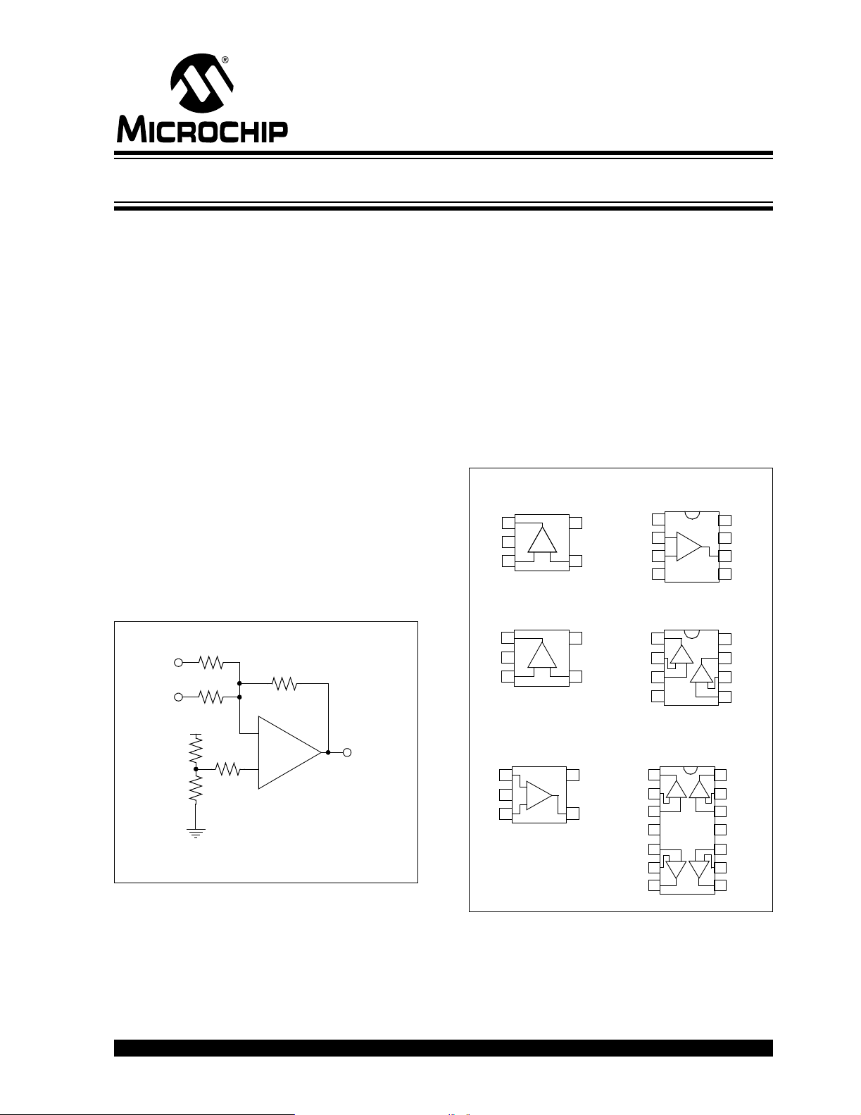
Typical Application
R
G2
V
IN2
R
G1
V
IN1
V
DD
R
X
R
Y
R
Z
Summing Amplifier Circuit
R
F
–
MCP6241
+
V
OUT
Description
The Microchip Technology Inc. MCP6241/2/4
operational amplifiers (op amps) provide wide
bandwidth for the quiescent current. The MCP6241/2/4
has a 550 kHz Gain Bandwidth Pro duct (GBWP) and
68° (typ.) phase ma rgin. This family operates from a
single supply voltage as low as 1.8V, while drawing
50 µA (typ.) quiescent current. In addition, the
MCP6241/2/4 family supports rail-to-rail input and
output swing, with a common mode input voltage range
+ 300 mV to VSS– 300 mV. These op amps are
of V
DD
designed in one of Microchip’s advanced CMOS
processes.
Package Types
MCP6241
SOT-23-5
V
V
1
1
OUT
OUT
V
V
VIN+
SS
SS
+
+
2
2
3
3
–
MCP6241R
SOT-23-5
V
1
OUT
V
DD
VIN+
+
2
–
3
MCP6241U
SC-70-5, SOT-23-5
VIN+
1
V
VIN–
SS
+
2
–
3
V
V
5
5
DD
DD
VIN–
4
4
V
V
5
SS
VIN–
4
V
V
5
DD
V
V
V
4
OUT
V
V
V
MCP6241
PDIP, SOIC, MSOP
1
NC
2
–
V
IN
VIN+
V
–
+
3
4
SS
MCP6242
PDIP, SOIC, MSOP
1
OUTA
_
V
2
-
INA
V
INA
V
SS
+
+
3
+
-
4
MCP6244
PDIP, SOIC, TSSOP
OUTA
INA
INA
V
DD
INB
INB
OUTB
1
–
-
2
+
3
4
+
5
-
–
6
7
14
+-+
13
12
11
10
-
+
+
8
NC
V
7
DD
6
V
OUT
5
NC
V
8
DD
7
V
OUTB
_
6
V
INB
5
V
+
INB
V
OUTD
V
–
IND
V
+
IND
V
SS
+
V
INC
9
–
V
INC
8
V
OUTC
© 2005 Microchip Technology Inc. DS21882C-page 1
MCP6241/2/4
1.0 ELECTRICAL CHARACTERISTICS
Absolute Maximum Ratings †
VDD – VSS........................................................................7.0V
All Inputs and Outputs ................... V
Difference Input Voltage ......................................|V
Output Short Circuit Current ..................................continuous
Current at Input Pins ....................................................±2 mA
Current at Output and Supply Pins ............................±30 mA
Storage Temperature.................................... .-65°C to +150°C
Maximum Junction Temperature (T
ESD Protection On All Pins (HBM;MM)............... ≥ 4 kV; 300V
– 0.3V to VDD + 0.3V
SS
– VSS|
DD
)..........................+150°C
J
† Notice: Stresses above those listed under “Absolute
Maximum Ratings” may cause permanent damage to the
device. This is a stress rating only and functional operation of
the device at those or any other conditions above those
indicated in the operational listings of this specification is not
implied. Exposure to maximum rating conditions for extended
periods may affect device reliability.
DC ELECTRICAL CHARACTERISTICS
Electrica l Character istics: Unless otherwise indicated, TA = +25°C, VDD = +1.8V to +5.5V, VSS = GND,
V
= VDD/2, RL = 100 kΩ to VDD/2 and V
CM
Parameters Sym Min Typ Max Units Conditions
Input Offset
Input Offset Voltage V
Extended Temperature V
Input Offset Drift with
ΔVOS/ΔT
Temperature
Power Supply Rejection PSRR — 83 — dB VCM = V
Input Bias Current and Impedance
Input Bias Current: I
At Temperature I
At Temperature I
Input Offset Current I
Common Mode Input Impedance Z
Differential Input Impedance Z
DIFF
Common Mode
Common Mode Input Range V
CMR
Common Mode Rejection Ratio CMRR 60 75 — dB V
Open-Loop G ain
DC Open-Loop Gain
A
(large signal)
Output
Maximum Output Voltage Swing VOL, VOHVSS + 35 — VDD – 35 mV RL = 10 kΩ, 0.5V Output
Output Short-Circuit Current I
I
Power Supply
Supply Voltage V
Quiescent Current per Amplifier I
Note:
The SC-70 package is only tested at +25°C.
OS
OS
OS
CM
OL
SC
SC
DD
Q
≈ V
OUT
/2.
DD
-5.0 — +5.0 mV VCM = V
SS
-7.0 — +7.0 mV TA= -40°C to +125°C,
= VSS (Note)
V
CM
—±3.0—µV/°CT
A
B
B
B
—±1.0—pA
—20—pAT
— 1100 — pA TA = +125°C
= -40°C to +125°C,
A
V
= V
CM
SS
SS
= +85°C
A
—±1.0—pA
—1013||6 — Ω||pF
—1013||3 — Ω||pF
V
– 0.3 — V
SS
90 110 — dB V
+ 0.3 V
DD
= -0.3V to 5.3V, V
CM
= 0.3V to VDD – 0.3V,
OUT
V
CM=VSS
Overdrive
—±6—mAV
—±23—mAV
DD
DD
= 1.8V
= 5.5V
1.8 — 5.5 V
30 50 70 µA IO = 0, VCM = VDD – 0.5V
DD
= 5V
DS21882C-page 2 © 2005 Microchip Technology Inc.
MCP6241/2/4
AC ELECTRICAL CHARACTERISTICS
Electrica l Character istics: Unless otherwise indicated, TA = +25°C, VDD = +1.8 to 5.5V, VSS = GND, VCM = VDD/2,
≈ VDD/2, RL = 10 kΩ to VDD/2 and CL = 60 pF.
V
OUT
Parameters Sym Min Typ Max Units Conditions
AC Response
Gain Bandwidth Product GBWP — 550 — kHz
Phase Margin PM — 68 — ° G = +1
Slew Rate SR — 0.30 — V/µs
Noise
Input Noise Voltage E
Input Noise Voltage Density e
Input Noise Current Density i
ni
ni
ni
—10—µV
—45—nV/√Hz f = 1 kHz
—0.6—fA/√Hz f = 1 kHz
TEMPERATURE CHARACTERISTICS
Electrica l Character istics: Unless otherwise indicated, VDD = +1.8V to +5.5V and VSS = GND.
Parameters Sym Min Typ Max Units Conditions
Temperature Ranges
Extended Temperature Range T
Operating Tempe rature Range T
Storage Temperature Range T
A
A
A
Thermal Package Resistances
Thermal Resistance, 5L-SC70
Thermal Resistance, 5L-SOT-23
Thermal Resistance, 8L-MSOP θ
Thermal Resistance, 8L-PDIP θ
Thermal Resistance, 8L-SOIC θ
Thermal Resistance, 14L-PDIP θ
Thermal Resistance, 14L-SOIC θ
Thermal Resistance, 14L-TSSOP θ
θ
JA
θ
JA
JA
JA
JA
JA
JA
JA
Note: The internal Junction Temperature (TJ) must not exceed the Absolute Maximum specification of +150°C.
-40 — +125 °C
-40 — +125 °C (Note)
-65 — +150 °C
—
—
331
256
—
—
—206—°C/W
—85—°C/W
—163—°C/W
—70—°C/W
—120—°C/W
—100—°C/W
f = 0.1 Hz to 10 Hz
P-P
°C/W
°C/W
© 2005 Microchip Technology Inc. DS21882C-page 3
MCP6241/2/4
5
:
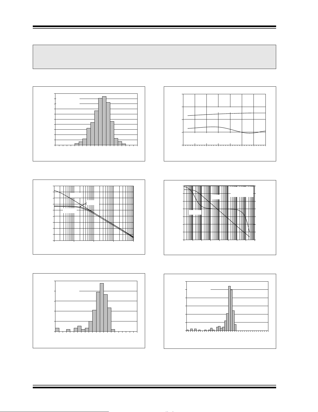
2.0 TYPICAL PERFORMANCE CURVES
Note: The grap hs and tables provided fol lowi ng this note are a st a tis tic al s umm ary based on a limite d number of
samples and are provided for informational purposes only. The performance characteristics listed herein
are not tested or guaranteed. In some graphs or tables, the data presented may be outside the specified
operating range (e.g., outside specified power supply range) and therefore outside the warranted range.
Note: Unless otherwise indicated, TA = +25°C, VDD = +1.8V to +5.5V, VSS = GND, VCM = VDD/2, V
= 100 kΩ to VDD/2 and CL = 60 pF.
R
L
OUT
≈ VDD/2,
20%
630 Samples
Percentage of Occurrences
18%
16%
14%
12%
10%
8%
6%
4%
2%
0%
= V
V
CM
SS
0
1
2
-5
-4
-3
-2
-1
Input Offset Voltage (mV)
3
FIGURE 2-1: Input Offset Voltage.
110
100
90
80
70
60
50
PSRR, CMRR ( dB )
40
30
20
10 1k 10k 100k100
1.E+01 1.E+02 1.E+03 1.E+04 1.E+0
PSRR-
CMRR
PSRR+
Frequency (Hz)
90
85
80
75
CMRR, PSRR (dB)
4
5
CMRR (VCM = -0.3V to +5.3V,
70
-50-25 0 255075100125
PSRR (VCM = VSS)
= 5.0V)
V
DD
Ambient Temperature (°C)
FIGURE 2-4: CMRR, PSRR vs. Ambient Temperature.
120
100
80
60
Phase
40
20
Open-Loop Gain (dB)
0
-20
0.1 1 10 100 1k 10k 100k 1M 10M
1.E-011.E+001.E+011.E+021.E+031.E+041.E+051.E+061.E+
Gain
Frequency (Hz)
RL = 10.0 k
= VDD/2
V
CM
0
-30
-60
-90
-120
-150
Open-Loop Phase (°)
-180
-210
07
FIGURE 2-2: PSRR, CMRR vs. Frequency.
25%
180 Samples
= VDD/2
V
CM
20%
= +85°C
T
A
15%
10%
5%
Percentage of Occurrences
0%
0
6
12
18
24
30
36
Input Bias Current (pA)
42
FIGURE 2-3: Input Bias Current at +85°C.
FIGURE 2-5: Open-Loop Gain, Phase vs.
Frequency.
30%
180 Samples
V
5%
0%
= VDD/2
CM
T
= +125°C
A
0.0
0.2
0.4
0.6
0.8
Input Bias Current (nA)
1.0
1.2
1.4
1.6
1.8
2.0
25%
20%
15%
10%
Percentage of Occurrences
FIGURE 2-6: Input Bias Current at +125°C.
DS21882C-page 4 © 2005 Microchip Technology Inc.
MCP6241/2/4
= +125°C
= +125°C
5
Note: Unless otherwise indicated, TA = +25°C, VDD = +1.8V to +5.5V, VSS = GND, VCM = VDD/2, V
= 100 kΩ to VDD/2 and CL = 60 pF.
R
L
10,000
1,000
Hz)
(nV/
100
Input Noise Voltage Density
10
0.1 100 1k 10k 100k101
1.E-01 1.E+001.E+011.E+021.E+031.E+041.E+0
Frequency (Hz)
5
FIGURE 2-7: Input Noise Voltage Density
20%
628 Samples
18%
V
= V
CM
SS
TA = -40°C to +125°C
-8-6-4
-12
-10
Input Offset Voltage Drift (µV/°C)
-2
0
Percentage of Occurrences
16%
14%
12%
10%
8%
6%
4%
2%
0%
FIGURE 2-10: Input Offset Voltage Drift.
vs. Frequency.
700
650
600
550
500
450
VDD = 1.8V
400
350
Input Offset Voltage (µV)
300
0.0 0.5 1.0 1.5 2.0 2.5 3.0 3.5 4.0 4.5 5.0 5.5
Output Voltage (V)
VCM = V
Input Offset Voltage (µV)
300
200
100
-100
-200
-300
0
TA = -40°C
T
T
T
-0.4
= +25°C
A
= +85°C
A
A
0.0
0.2
0.4
0.6
0.8
-0.2
Common Mode Input Voltage (V)
1.0
1.2
VDD = 1.8V
1.4
1.6
1.8
2.0
2.2
≈ VDD/2,
OUT
2
4
SS
VDD = 5.5V
6
8
10
12
FIGURE 2-8: Input Offset Voltage vs.
Common Mode Input Voltage at V
400
300
200
100
TA = -40°C
0
T
= +25°C
A
T
= +85°C
A
-100
T
-200
A
0.0
0.5
1.0
1.5
2.0
-0.5
Common Mode Input Voltage (V)
2.5
3.0
Input Offset Voltage (µV)
3.5
= 1.8V.
DD
VDD = 5.5V
4.0
4.5
5.0
5.5
6.0
FIGURE 2-9: Input Offset Voltage vs.
Common Mode Input Voltage at V
= 5.5V.
DD
FIGURE 2-11: Input Offset Voltage vs. Output Voltage.
35
30
25
20
15
10
5
0
-5
-10
-15
-20
-25
Short Circuit Current (mA)
-30
-35
0.00.51.01.52.02.53.03.54.04.55.05.
Power Supply Voltage (V)
+I
SC
-I
SC
TA = +125°C
T
= +85°C
A
T
= +25°C
A
T
= -40°C
A
FIGURE 2-12: Output Short-Circuit Current vs. Ambient Temperature.
© 2005 Microchip Technology Inc. DS21882C-page 5
MCP6241/2/4
1
6
Max. Output Voltage Swing
:
Note: Unless otherwise indicated, TA = +25°C, VDD = +1.8V to +5.5V, VSS = GND, VCM = VDD/2, V
= 100 kΩ to VDD/2 and CL = 60 pF.
R
L
0.50
0.45
0.40
Falling Edge
0.35
0.30
0.25
Slew Rate (V/µs)
0.20
0.15
Rising Edge
0.10
-50 -25 0 25 50 75 100 125
FIGURE 2-13: Slew Rate vs. Ambient Temperature.
1,000
100
(mV)
10
Output Voltage Headroom
1
1.E-02 1.E-01 1.E+00 1.E+0
VDD = 5.5V
VDD = 1.8V
Ambient Temperature (°C)
VDD – V
OH
VOL – V
100µ10µ
Output Current Magnitude (A )
Output Voltage (10 mV/div)
Time (1 µs/div)
FIGURE 2-16: Sm al l-Signal, Non-Inverting Pulse Response.
5.0
4.5
4.0
3.5
3.0
SS
10m1m
2.5
2.0
1.5
Output Voltage (V)
1.0
0.5
0.0
Time (10 µs/div)
OUT
≈ VDD/2,
G = +1 V/V
R
= 10 k
L
VDD = 5.0V
G = +1 V/V
FIGURE 2-14: Output Voltage Headroom vs. Output Current Magnitude.
10
VDD = 5.5V
)
VDD = 1.8V
P-P
1
(V
0.1
1k 10k 100k 1M
1.E+03 1.E+04 1.E+05 1.E+0
Frequency (Hz)
FIGURE 2-15: Maximum Output Voltage Swing vs. Frequency.
FIGURE 2-17: Large-Signal, Non-Inverting Pulse Response.
80
VCM = 0.9V
70
60
50
40
30
20
per Amplifier (µA)
Quiescent Current
10
0
0.0 0.5 1.0 1.5 2.0 2.5 3.0 3.5 4.0 4.5 5.0 5.5
DD
TA = +125°C
T
T
T
Power Supply Voltage (V)
= +85°C
A
= +25°C
A
= -40°C
A
FIGURE 2-18: Quiescent Current vs. Power Supply Voltage.
DS21882C-page 6 © 2005 Microchip Technology Inc.

MCP6241/2/4
3.0 PIN DESCRIPTIONS
Descriptions of the pins are listed in Table 3-1 (single op amps) and Table 3-2 (dual and quad op amps).
TABLE 3-1: PIN FUNCTION TABLE FOR SINGLE OP AMPS
MCP6241
(PDIP, SOIC, MSOP)
6114V
2443V
3331V
7525V
4252V
1, 5, 8 — — — NC No Internal Connection
TABLE 3-2: PIN FUNCTION TABLE FOR DUAL AND QUAD OP AMPS
MCP6242 MCP6244 Symbol Description
11V
22V
33V
84V
55V
66V
77V
—8V
—9V
—10V
411V
—12V
—13V
—14V
MCP6241
(SOT-23-5)
MCP6241R
(SOT-23-5)
OUTA
– Inverting Input (op amp A)
INA
+ Non-inverting Input (op amp A)
INA
DD
+ Non-inverting Input (op amp B)
INB
– Inverting Input (op amp B)
INB
OUTB
OUTC
– Inverting Input (op amp C)
INC
+ Non-inverting Input (op amp C)
INC
SS
+ Non-inverting Input (op amp D)
IND
– Inverting Input (op amp D)
IND
OUTD
MCP6241U
(SOT-23-5)
Analog Output (op amp A)
Positive Power Supply
Analog Output (op amp B)
Analog Output (op amp C)
Negative Power Supply
Analog Output (op amp D)
Symbol Description
OUT
IN
IN
Analog Outp ut
– Inverting Input
+ Non-inverting Input
Positive Power Supply
DD
Negative Power Supply
SS
3.1 Analog Outputs
The output pins are low-impedance voltage sources.
3.2 Analog Inputs
The non-inverting and inverting inputs are highimpedance CMOS inputs with low bias currents.
3.3 Power Supply (VSS and VDD)
The positive powe r s upp ly (VDD) is 1.8V to 5.5V h igh er
than the negative power supply (V
operation, the other pins are between V
Typically, these parts are used in a single-(positive)
supply configuration. In this case, V
ground and V
is connected to the supply. VDD will
DD
). For normal
SS
and VDD.
SS
is connected to
SS
need a local bypass capacitor (typically 0.01µF to
0.1 µF) within 2 mm of the VDD pin. These parts can
share a bulk capacitor (typically 1 µ F to 100 µF) with
other nearby analog part s; it needs to be within 100 mm
of the V
© 2005 Microchip Technology Inc. DS21882C-page 7
DD
pin.
MCP6241/2/4
4.0 APPLICATION INFORMATION
The MCP6241/2/4 family of op amps is manufactured
using Microchip’s state-of-the-art CMOS process and
is specifically designed for low-power and generalpurpose applications. The low supply voltage, low
quiescent current and wide bandwidth makes the
MCP6241/2/4 ideal for battery-powered applications.
4.1 Rail-to-Rail Inputs
The MCP6241/2/4 op amps are designed to prevent
phase reversal when the input pins exceed the supply
voltages. Fi gure 4-1 shows the input volt age excee ding
the supply voltage without any phase reversal.
6
V
5
4
3
2
1
0
Input, Output Voltage (V)
-1
V
OUT
IN
Time (1 ms/div)
FIGURE 4-1: The MCP6241/2/4 Show No Phase Reversal.
The input stage of the MCP6241/2/4 op amps use two
differential input s tages in paralle l. One op erates at low
common mode input voltage (VCM) and the other at
high V
V
CM
The Input Offset Voltage is measured at
VCM=VSS– 300 mV and VDD+ 300 mV to ensure
proper operation.
Input voltages that exceed the input voltage range
(V
excessive current to flow into or out of the input pins.
Current beyond ±2 mA can cause reliability problems.
Applications that exceed this rating must be externally
limited with a resistor, as shown in Figure 4-2.
. With this topology, the device operates with
CM
up to 300 mV above VDD and 300 mV below VSS.
– 0.3V to VDD+ 0.3V at 25°C) can cause
SS
VDD = 5.0V
G = +2 V/V
–
IN
V
OUT
R
IN
V
IN
Maximum expected V
()VDD–
------------------------------------------------------------------------------ -
R
≥
IN
VSSMinimum expected V
----------------------------------------------------------------------------
R
≥
IN
MCP624X
+
IN
2 mA
()–
2 mA
FIGURE 4-2: Input Current-Limiting
Resistor (R
IN
).
4.2 Rail-to-Rail Output
The output volt age rang e of the MC P6241/2/4 op a mps
– 35 mV (max.) and VSS + 35 mV (min.) when
is V
DD
=10kΩ is connected to VDD/2 and VDD = 5.5V.
R
L
Refer to Figure 2 -14 for more information.
4.3 Capacitive Loads
Driving large capacitive loads can cause stability
problems for voltage-feedback op amps. As the load
capacitance increases, the feedback loop’s phase
margin decreases and the closed-loop bandwidth is
reduced. This produces gain peaking in the frequency
response, with overshoot and ringing in the step
response. A unity-gain buffer (G = +1) is the most
sensitive to capacitive loads, but all gains show the
same general behavior.
When driving large capacitive loads with these op
amps (e.g., > 70 pF when G = +1), a small series
resistor at the output (R
feedback loop’s phase margin (stability) by making the
output load resistive at higher frequencies. The
bandwidth will be generally lower than the bandwidth
with no capac itive load.
–
MCP624X
V
IN
+
in Figure 4-3) improves the
ISO
R
ISO
C
L
V
OUT
FIGURE 4-3: Output resistor, R
ISO
stabiliz es large capacitive loads.
Figure 4-4 gives recommended R
different capacitive loads and gains. The x-axis is the
normalized load capacitance (C
L/GN
circuit’s nois e gain. For non -inverting ga ins, G
signal gain are equal. For inverting gains, G
1 + |Signal Gain| (e.g., –1 V/V gives G
DS21882C-page 8 © 2005 Microchip Technology Inc.
values for
ISO
), where GN is the
and the
N
is
= +2 V/V).
N
N
MCP6241/2/4
:
1.E+04
10k
)
(
ISO
1k
1.E+03
Recommended R
100
1.E+02
10p 100p 1n 10n
1.E+01 1.E+02 1.E+03 1.E+04
Normalized Load Capacitance; C
FIGURE 4-4: Recommended R
GN = +1 V/V
G
t +2 V/V
N
L/GN
(F)
ISO
Values
for Capacitive Loads.
After sele cting R
resulting frequency response peaking and step
response overshoot. Evaluation on the bench and
simulations with the MCP6241/2/4 SPICE macro
model are very helpful. Modify R
response is reasonable.
for your circuit, double-check the
ISO
’s value until the
ISO
4.4 Supply Bypass
With this op amp, the power supply pin (VDD for
single-supply) should have a local bypass capacitor
(i.e., 0.01 µF to 0.1 µF) within 2 mm for good highfrequency performance. It can use a bulk capacitor
(i.e., 1 µF or larger ) within 100 mm to provide la rge,
slow currents. This bu lk capaci tor can be sh ar ed with
other nearby analog parts.
4.5 Unused Op Amps
An unused op amp in a quad package (MCP6244)
should be configured as shown in Figure 4-5. Both
circuits prevent the output from toggling and causing
crosstalk. Circuit A can use any reference voltage
between the supplies, provides a buffered DC voltage,
and minimizes the supply current draw of the unused
op amp. Circuit B minimizes the number of
components, but may draw a little more supply current
for the unused op amp.
¼ MCP6244 (A) ¼ MCP6244 (B)
V
DD
V
DD
4.6 PCB Surface Leakage
In applications where low input bias current is critical,
PCB (printed circuit board) surface leakage effects
need to be considered. Surface leakage is caused by
humidity, dust or other contamination on the board.
Under low humidity conditions, a typical resistance
between nearby traces is 1 0
cause 5 pA of current to flow, which is greater than the
MCP6241/2/4 family’ s bias c urrent at 25°C (1 pA, typ.).
The easiest way to reduce surface leakage is to use a
guard ring around se nsi tiv e p ins (or t race s). The gua rd
ring is biased at the same voltage as the sensitive pin.
An example of this type of layout is shown in
Figure 4-6.
VIN-V
FIGURE 4-6: Example Guard Ring Layout for Inverting Gain.
1. Non-inverting Gain and Unity-Gain Buffer:
a. Connect the non-inverting pin (V
input with a wire that does not touch the
PCB surface.
b. Connect the guard ring to th e inverting input
–). This biases the g uard rin g t o th e
pin (V
IN
common mode input voltage.
2. Inverting Gain and Transimpedance Amplifiers
(convert current to voltage, such as photo
detectors):
a. Connect the guard ring to the non-inverting
input pin (V
to the same reference voltage as the op
amp (e.g., V
b. Connect the inverting pin (VIN–) to the input
with a wire that does not touch the PCB
surface.
12
Ω. A 5V dif ference would
+
IN
V
SS
Guard Ring
+) to the
IN
+). This bi ases the gua rd ri ng
IN
/2 or ground).
DD
V
DD
FIGURE 4-5: Unused Op Amps.
© 2005 Microchip Technology Inc. DS21882C-page 9

MCP6241/2/4
4.7 Application Circuits
4.7.1 MATCHING THE IMPEDANCE AT
THE INPUTS
To minimize the effect of offset voltage in an amplifier
circuit, the impedances at the inverting and noninverting inputs need to be matched. This is done by
choosing the circuit resistor values so that the total
resistance at each input is the same. Figure 4-7 shows
a summing amplifier circuit.
R
G2
V
IN2
R
G1
V
IN1
V
DD
R
X
R
Y
R
Z
FIGURE 4-7: Summing Amplifier Circuit.
To match the inputs, set all voltage sources to ground
and calculate the to tal resistance at t he inp ut n ode s. In
this summing amplifier circuit, the resistance at the
inverting input is calculated by setting V
V
to ground. In this case, RG1, RG2 and RF are in
OUT
parallel. The total resistance at the inverting input is:
R
–
=
VIN
Where:
–
= total resist ance a t th e inv erting i nput
R
VIN
R
F
–
------
R
V
OUT
, V
IN2
and
IN1
1
F
MCP624X
+
1
---------
++
R
G1
1
1
---------
R
G2
---------------------------------------------
⎛⎞
⎝⎠
4.7.2 COMPENSATING FOR THE
PARASITIC CAPACITANCE
In analog circuit design, the PC B p a rasi tic ca p ac it a nc e
can compromise the circuit beh avior; Figure4-8 shows
a typical scenario. If the input of an amplifier sees
parasitic capacitance of several picofarad (C
PARA
which includes th e comm on mo de cap a cit anc e of 6 pF,
typical) and large R
and RG, the frequency response
F
of the circuit will include a zero. This parasitic zero
introduces gain peaking and can cause circuit
instability.
V
AC
R
C
G
PARA
V
DC
+
MCP624X
–
R
F
C
F
CFC
V
PARA
OUT
R
G
-------
•=
R
F
FIGURE 4-8: Effect of Parasitic Capacitance at the Input.
One solution is to use s maller res istor valu es to push
the zero to a higher frequency. Another solution is to
compensate by introd uc ing a pole at the point at which
the zero occurs. This can be done by adding C
parallel with the f eedbac k resi stor (R
selected so that the rati o C
F:RG
.
of R
PARA:CF
). CF needs to be
F
is equal to the ratio
in
F
,
At the non-inverting input, V
source. When V
is set to ground, bot h RX and RY are
DD
is the only voltage
DD
in parallel. The total resistance at the non-inverting
input is:
1
R
VIN
-------------------------
+
1
⎛⎞
------
+
⎝⎠
R
X
----- -
R
+=
R
Z
1
Y
Where:
+
R
= total resistance at the inverting
VIN
input
To minimize offset voltage and increase circuit
accuracy, the resistor values need to meet the
condition:
R
VIN
DS21882C-page 10 © 2005 Microchip Technology Inc.
R
VIN
–=
+

5.0 DESIGN TOOLS
Microchip provides the basic design tools needed for
the MCP6241/2/4 family of op amps.
5.1 SPICE Macro Model
The latest SPICE macro model for the MCP6241/2/4 op
amps is available on our web site at
www.microchip.com. This model is intended to be an
initial design tool that wo rks well in t he op amp’s linear
region of operation at room temperature. See the macro
model file for information on its capabilities.
Bench testing is a very im portant par t of any design an d
cannot be replaced with simulations. Also, simulation
results using th is ma cro m od el ne ed to be v ali dated by
comparing them to the data sheet spec ifications and
characteristic curves.
5.2 FilterLab® Software
Microchip’s Fi lte rLab so ftw are is an inno vativ e tool th at
simplifies analog active-filter (using op amps) design.
Available at no cost from our web site at
www.m ic roc hi p.c om , th e Fil terLa b des ig n tool provides
full schematic diagrams of the filter circuit with
component values. It also outputs the filter circuit in
SPICE format, which can be used with the macro
model to simulate actual filter performance.
MCP6241/2/4
© 2005 Microchip Technology Inc. DS21882C-page 11

MCP6241/2/4
6.0 PACKAGING INFORMATION
6.1 Package Marking Information
5-Lead SC-70 (MCP6241U Only)
XXN (Front)
YWW (Back)
5-Lead SOT-23
5
XXNN
1 23
8-Lead MSOP
XXXXXX
YWWNNN
8-Lead PDIP (300 mil)
OR
4
XXNN
MCP6241 BQNN
MCP6241R BRNN
MCP6241U BSNN
Example:
A T2 (Fron t)
546 (Back)
Device Code
Note: Applies to 5-Lead SOT-23.
OR
Example:
5
BQ25
1 23
Example:
6242E
546256
Example:
AT25
4
XXXXXXXX
XXXXXNNN
YYWW
8-Lead SOIC (150 mil)
XXXXXXXX
XXXXYYWW
NNN
Legend: XX...X Customer-specific information
Y Year code (last digit of calendar year)
YY Year code (last 2 digits of calendar year)
WW Week code (week of January 1 is week ‘01’)
NNN Alphanumeric traceability code
3
e
Pb-free JEDEC designator for Matte Tin (Sn)
* This package is Pb-free. The Pb-fr ee JEDEC designator ( )
can be found on the outer packaging for this package.
Note: In the event the full Microchip part nu mber ca nn ot be marked o n one lin e, it will
be carried over to the next line, thus limiting the number of available
characters for customer-specific information.
MCP6242
e
E/P ^^256
0546
Example
MCP6242E
3
e
SN^^ 0546
256
3
:
3
e
DS21882C-page 12 © 2005 Microchip Technology Inc.

Package Marking Information (Continued)
14-Lead PDIP (300 mil) (MCP6244)Example:
MCP6241/2/4
XXXXXXXXXXXXXX
XXXXXXXXXXXXXX
YYWWNNN
14-Lead SOIC (150 mil) (MCP6244)
XXXXXXXXXX
XXXXXXXXXX
YYWWNNN
14-Lead TSSOP (MCP6244)
XXXXXXXX
YYWW
NNN
Example:
Example:
6244E
0546
256
MCP6244
e
E/P^^
0546256
MCP6244
E/SL^^
0546256
3
3
e
© 2005 Microchip Technology Inc. DS21882C-page 13

MCP6241/2/4
5-Lead Plastic Small Outline Transistor Package (LT) (SC-70)
E
E1
D
p
n
Q1
c
Number of Pins
Pitch
Molded Package Thickness
Standoff
Molded Package Width
Top of Molded Pkg to Lead Shoulder
Lead Thickness
A2
A1
E1
Q1
B
1
A2
A1
L
MILLIMETERS*INCHESUnits
MINDimension Limits
n
p
c
NOM
.004 .016 0.10 0.40
MINMAX
NOM
55
0.65 (BSC).026 (BSC)
A
MAX
1.100.80.043.031AOverall Height
1.000.80.039.031
0.100.00.004.000
2.401.80.094.071EOverall Width
1.351.15.053.045
2.201.80.087.071DOverall Length
0.300.10.012.004LFoot Length
0.180.10.007.004
0.300.15.012.006BLead Width
*Controlling Parameter
Notes:
Dimensions D and E1 do not include mold flash or protrusions. Mold flash or protrusions shall not
exceed .005" (0.127mm) per side.
JEITA (EIAJ) Standard: SC-70
Drawing No. C04-061
DS21882C-page 14 © 2005 Microchip Technology Inc.

5-Lead Plastic Small Outline Transistor (OT) (SOT23)
E
E1
p
B
p1
D
MCP6241/2/4
n
c
β
Number of Pins
Pitch
Outside lead pitch (basic)
Foot Angle
Lead Thickness
Mold Draft Angle Top
Mold Draft Angle Bottom
*Controlling Parameter
Notes:
Dimensions D and E1 do not include mold flash or protrusions. Mold flash or protrusions shall not
exceed .005" (0.127mm) per side.
1
A
φ
L
n
p
p1
φ
c
α
β
A1
.038
α
A2
MILLIMETERSINCHES*Units
MAXNOMMINMAXNOMMINDimension Limits
55
0.95
1.90.075
1.451.180.90.057.046.035AOverall Height
1.301.100.90.051.043.035A2Molded Package Thickness
0.150.080.00.006.003.000A1Standoff
3.002.802.60.118.110.102EOverall Width
1.751.631.50.069.064.059E1Molded Package Width
3.102.952.80.122.116.110DOverall Length
0.550.450.35.022.018.014LFoot Length
10501050
0.200.150.09.008.006.004
0.500.430.35.020.017.014BLead Width
10501050
10501050
EIAJ Equivalent: SC-74A
Drawing No. C04-091
© 2005 Microchip Technology Inc. DS21882C-page 15

MCP6241/2/4
8-Lead Plastic Micro Small Outline Package (MS) (MSOP)
E
E1
p
D
2
B
n 1
α
A
c
(F)
β
Units
Dimension Limits
Number of Pins
Pitch
Overall Height
Molded Package Thickness
Standoff
Overall Width
Molded Package Width
Overall Length
Foot Length
Foot Angle
Lead Thickness
Lead Width
Mold Draft Angle Top
Mold Draft Angle Bottom
*Controlling Parameter
Notes:
Dimensions D and E1 do not include mold flash or protrusions. Mold flash or protrusions shall not
exceed .010" (0.254mm) per side.
JEDEC Equivalent: MO-187
Drawing No. C04-111
p
A2
A1
E
E1
D
L
B
α
MIN
n
A
φ
c
β
INCHES
.026 BSC
.030
.000
.193 TYP.
.118 BSC
.118 BSC
.016 .024
.037 REFFFootprint (Reference)
0° - 8°
.003
.009
5°
5° -
L
NOM
8
.033
.006
.012
φ
A1
MAX NOM
--
-
-
.043
.037
.006
.031
.009
.016
15°
15°
MIN
0.75
0.00
0.40
0.08
0.22
MILLIMETERS*
MAX
8
0.65 BSC
--
0.85
-
4.90 BSC
3.00 BSC
3.00 BSC
0.60
0.95 REF
0°
-
-
-
A2
1.10
0.95
0.15
0.80
8°
0.23
0.40
15°5° 15°5° -
DS21882C-page 16 © 2005 Microchip Technology Inc.

8-Lead Plastic Dual In-line (P) – 300 mil (PDIP)
E1
D
2
MCP6241/2/4
n
E
β
eB
Number of Pins
Pitch
Top to Seating Plane A .140 .155 .170 3.56 3.94 4.32
Molded Package Thickness A2 .115 .130 .145 2.92 3.30 3.68
Base to Seating Plane A1 .015 0.38
Shoulder to Shoulder Width E .300 .313 .325 7.62 7.94 8.26
Molded Package Width E1 .240 .250 .260 6.10 6.35 6.60
Overall Length D .360 .373 .385 9.14 9.46 9.78
Tip to Seating Plane L .125 .130 .135 3.18 3.30 3.43
Lead Thickness
Upper Lead Width B1 .045 .058 .070 1.14 1.46 1.78
Lower Lead Width B .014 .018 .022 0.36 0.46 0.56
Overall Row Spacing § eB .310 .370 .430 7.87 9.40 10.92
Mold Draft Angle Top
Mold Draft Angle Bottom
* Controlling Parameter
§ Significant Characteristic
Notes:
Dimensions D and E1 do not include mold flash or protrusions. Mold flash or protrusions shall not exceed
.010” (0.254mm) per side.
JEDEC Equivalent: MS-001
Drawing No. C04-018
Dimension Limits MIN NOM MAX MIN NOM MAX
1
α
A
c
Units INCHES* MILLIMETERS
n
p
c
α
β
.008 .012 .015 0.20 0.29 0.38
A1
B1
B
88
.100 2.54
51015 51015
51015 51015
A2
L
p
© 2005 Microchip Technology Inc. DS21882C-page 17

MCP6241/2/4
8-Lead Plastic Small Outline (SN) – N arrow, 150 mil (SOIC)
E
E1
p
D
2
B
Number of Pins
Pitch
Foot Angle
Lead Thickness
Mold Draft Angle Top
Mold Draft Angle Bottom
* Controlling Parameter
§ Significant Characteristic
Notes:
Dimensions D and E1 do not include mold flash or protrusions. Mold flash or protrusions shall not exceed
.010” (0.254mm) per side.
JEDEC Equivalent: MS-012
Drawing No. C04-057
n
45°
c
β
n
p
φ
c
α
β
1
h
A
φ
L
048048
A1
MILLIMETERSINCHES*Units
1.27.050
α
A2
MAXNOMMINMAXNOMMINDimension Limits
88
1.751.551.35.069.061.053AOverall Height
1.551.421.32.061.056.052A2Molded Package Thickness
0.250.180.10.010.007.004A1Standoff §
6.206.025.79.244.237.228EOverall Width
3.993.913.71.157.154.146E1Molded Package Width
5.004.904.80.197.193.189DOverall Length
0.510.380.25.020.015.010hChamfer Distance
0.760.620.48.030.025.019LFoot Length
0.250.230.20.010.009.008
0.510.420.33.020.017.013BLead Width
1512015120
1512015120
DS21882C-page 18 © 2005 Microchip Technology Inc.

14-Lead Plastic Dual In-line (P) – 300 mil (PDIP)
E1
D
2
MCP6241/2/4
n
E
β
eB
Number of Pins
Pitch
Top to Seating Plane A .140 .155 .170 3.56 3.94 4.32
Molded Package Thickness A2 .115 .130 .145 2.92 3.30 3.68
Base to Seating Plane A1 .015 0.38
Shoulder to Shoulder Width E .300 .313 .325 7.62 7.94 8.26
Molded Package Width
Overall Length D .740 .750 .760 18.80 19.05 19.30
Tip to Seating Plane L .125 .130 .135 3.18 3.30 3.43
Lead Thickness
Upper Lead Width B1 .045 .058 .070 1.14 1.46 1.78
Lower Lead Width B .014 .018 .022 0.36 0.46 0.56
Overall Row Spacing § eB .310 .370 .430 7.87 9.40 10.92
Mold Draft Angle Top
Mold Draft Angle Bottom
* Controlling Parameter
§ Significant Characteristic
Notes:
Dimensions D and E1 do not include mold flash or protrusions. Mold flash or protrusions shall not exceed
.010” (0.254mm) per side.
JEDEC Equivalent: MS-001
Drawing No. C04-005
1
A
c
A1
Dimension Limits MIN NOM MAX MI N NOM MAX
Units INCHES* MILLIMETERS
n
p
E1
c
α
β
.240 .250 .260 6.10 6.35 6.60
.008 .012 .015 0.20 0.29 0.38
5 10 15 5 10 15
5 10 15 5 10 15
B1
B
14 14
.100 2.54
α
A2
L
p
© 2005 Microchip Technology Inc. DS21882C-page 19

MCP6241/2/4
14-Lead Plastic Small Outline (SL) – Narrow, 150 mil (SOIC)
E
E1
p
D
2
B
n
1
45°
c
β
Number of Pins
Pitch
Foot Angle
Lead Thickne ss
Mold Draft Angle Top
Mold Draft Angle Bottom
* Controlling Parameter
§ Significant Characteristic
Notes:
Dimensions D and E1 do not include mold flash or protrusions. Mold flash or protrusions shall not exceed
.010” (0.254mm) per side.
JEDEC Equivalent: MS-012
Drawing No. C04-065
h
A
φ
L
n
p
φ
c
α
β
A1
048048
α
MILLIMETERSINCHES*Units
1.27.050
A2
MAXNOMMINMAXNOMMINDimension Limits
1414
1.751.551.35.069.061.053AOverall Height
1.551.421.32.061.056.052A2Molded Package Thickness
0.250.180.10.010.007.004A1Standoff §
6.205.995.79.244.236.228EOverall Width
3.993.903.81.157.154.150E1Mold ed Pa ckag e Width
8.818.698.56.347.342.337DOverall Length
0.510.380.25.020.015.010hChamfer Distance
1.270.840.41.050.033.016LFoot Length
0.250.230.20.010.009.008
0.510.420.36.020.017.014BLead Width
1512015120
1512015120
DS21882C-page 20 © 2005 Microchip Technology Inc.

14-Lead Plastic Thin Shrink Small Outline (ST) – 4.4 mm (TSSOP)
E
E1
p
D
2
n
B
1
MCP6241/2/4
A
c
φ
β
Number of Pins
Pitch
Foot Angle
Lead Thickne ss
Mold Draft Angle Top
Mold Draft Angle Bottom
* Controlling Parameter
§ Significant Characteristic
Notes:
Dimensions D and E1 do not include mold flash or protrusions. Mold flash or protrusions shall not exceed
.005” (0.127mm) per side.
JEDEC Equivalent: MO-153
Drawing No. C04-087
n
p
φ
c
α
β
L
MILLIMETERS*INCHESUnits
0.65.026
α
A2A1
MAXNOMMINMAXNOMMINDimension Limits
1414
1.10.043AOverall Height
0.950.900.85.037.035.033A2Mold ed Packag e Thickness
0.150.100.05.006.004.002A1Standoff §
6.506.386.25.256.251.246EOverall Width
4.504.404.30.177.173.169E1Molded Package Width
5.105.004.90.201.197.193DMolded Package Length
0.700.600.50.028.024.020LFoot Length
840840
0.200.150.09.008.006.004
0.300.250.19.012.010.007B1Lead Width
10501050
10501050
© 2005 Microchip Technology Inc. DS21882C-page 21

MCP6241/2/4
NOTES:
DS21882C-page 22 © 2005 Microchip Technology Inc.

APPENDIX A: REVISION HISTORY
Revision C (March 2005)
The following is the list of modifications:
1. Added the MCP6244 quad op amp.
2. Re-compensated parts. Specifications that
change are: Gain Bandwidth Product (BWP)
and Phase Margin (PM) in AC Electrical
Characteristics table.
3. Corrected plots in Section 2.0 “Typical Perfor-
mance Curves”.
4. Added Section 3.0 “Pin Descriptions”.
5. Added new SC-70 package markings. Added
PDIP-14, SOIC-14, and TSSOP-14 packages
and corrected package marking information
(Section 6.0 “Packaging Information”).
6. Added Appendix A: “Revision History”.
Revision B (August 2004)
Revision A (March 2004)
MCP6241/2/4
• Original Release of this Document.
© 2005 Microchip Technology Inc. DS21882C-page 23

MCP6241/2/4
NOTES:
DS21882C-page 24 © 2005 Microchip Technology Inc.

MCP6241/2/4
PRODUCT IDENTIFICATION SYSTEM
To order or obtain information, e.g., on pricing or delivery, refer to the factory or the listed sales office.
PART NO. -X /XX
Device
X
Tape and Reel
and/or
Range
PackageTemperature
Alternate Pinout
Device: MCP6241: Single Op Amp (MSOP, PDIP, SOIC)
MCP6241T: Single Op Amp (Tape and Reel)
MCP6241RT: Single Op Amp (Tape and Reel)
MCP6241UT: Single Op Amp (Tape and Reel)
MCP6242: Dual Op Amp
MCP6242T: Dual Op Amp (Tape and Reel)
MCP6244: Quad Op Amp
MCP6244T: Quad Op Amp (Tape and Reel)
(MSOP, SOIC, SOT-23)
(SOT-23)
(SC-70, SOT-23)
(MSOP, SOIC)
(SOIC, TSSOP)
Examples:
a) MCP6241-E/SN: Extended Temp.,
b) MCP6241-E/MS: Extended Temp.,
c) MCP6241-E/P: Extended Temp.,
d) MCP6241RT-E/OT: Tape and Reel,
e) MCP6241UT-E/OT: Tape and Reel,
f) MCP6241UT-E/LT: Tape and Reel,
8LD SOIC package.
8LD MSOP package.
8LD PDIP package.
Extended T emp.,
5LD SOT-23 package
Extended T emp.,
5LD SOT-23 package.
Extended T emp.,
5LD SC-70 package.
Temperature Range: E = -40°C to +125°C
Package: LT = Plastic Package (SC-70), 5-lead (MCP6241U only)
MS = Plastic Micro Small Outline (MSOP), 8-lead
P = Plastic DIP (300 mil Body), 8-lead, 14-lead
OT = Plastic Small Outline Transistor (SOT-23), 5-lead
(MCP6241, MCP6241R, MCP6241U)
SN = Plastic SOIC (150 mil Body), 8-lead
SL = Plastic SOIC (150 mil Body), 14-lead
ST = Plastic TSSOP (4.4 mil Body), 14-lead
a) MCP6242-E/SN: Extended Temp.,
8LD SOIC package.
b) MCP6242-E/MS: Extended Temp.,
8LD MSOP package.
c) MCP6242-E/P: Extended Temp.,
8LD PDIP package.
d) MCP6242T-E/SN: Tape and Reel,
Extended T emp.,
8LD SOIC package.
a) MCP6244-E/P: Extended Temp.,
14LD PDIP package.
b) MCP6244-E/SL: Extended Temp.,
14LD SOIC package.
c) MCP6244-E/ST: Extended T emp.,
14LD TSSOP
package.
d) MCP6244T-E/SL: Tape and Reel,
Extended T emp.,
14LD SOIC package.
e) MCP6244T-E/ST: Tape and Reel,
Extended T emp.,
14LD TSSOP
package.
© 2005 Microchip Technology Inc. DS21882C-page 25

MCP6241/2/4
NOTES:
DS21882C-page 26 © 2005 Microchip Technology Inc.

Note the following details of the code protection feature on Microchip devices:
• Microchip products meet the specification contained in their particular Microchip Data Sheet.
• Microchip believes that its family of products is one of the most secure families of its kind on the market today, when used in the
intended manner and under normal conditions.
• There are dishonest and possibly illegal methods used to breach the code protection feature. All of these methods, to our
knowledge, require using the Microchip products in a manner outside the operating specifications contained in Microchip’s Data
Sheets. Most likely, the person doing so is engaged in theft of intellectual property.
• Microchip is willing to work with the customer who is concerned about the integrity of their code.
• Neither Microchip nor any other semiconductor manufacturer can guarantee the security of their code. Code protection does not
mean that we are guaranteeing the product as “unbreakable.”
Code protection is constantly evolving. We at Microchip are committed to continuously improving the code protection features of our
products. Attempts to break Microchip’s code protection feature may be a violation of the Digital Millennium Copyright Act. If such acts
allow unauthorized access to your software or other copyrighted work, you may have a right to sue for relief under that Act.
Information contained in this publication regarding device
applications and the like is provided only for your convenience
and may be superseded by updates. It is your responsibility to
ensure that your application meets with your specifications.
MICROCHIP MAKES NO REPRESENTATIONS OR WARRANTIES OF ANY KIND WHETHER EXPRESS OR IMPLIED,
WRITTEN OR ORAL, STATUTORY OR OTHERWISE,
RELATED TO THE INFORMATION, INCLUDING BUT NOT
LIMITED TO ITS CONDITION, QUALITY, PERFORMANCE,
MERCHANTABILITY OR FITNESS FOR PURPOSE.
Microchip disclaims all liability arising from this information and
its use. Use of Mic rochip’s products as c ritical compon ents in
life support systems is not authorized except with express
written approval by Microchip. No licenses are conveyed,
implicitly or otherwise, under any Microchip intellectual property
rights.
Trademarks
The Microchip name and logo, the Microchip logo, Accuron,
dsPIC, K
EELOQ, microID, MPLAB, PIC, PICmi cro, PICST AR T ,
PRO MATE, PowerSmart, rfPIC, and SmartShunt are
registered trademarks of Microchip Technology Incorporated
in the U.S.A. and other countries.
AmpLab, FilterLab, Migratable Memory, MXDEV, MXLAB,
PICMASTER, SEEVAL, SmartSensor and The Embedded
Control Solutions Company are registered trademarks of
Microchip Technology Incorporated in the U.S.A.
Analog-for-the-Digital Age, Application Maestro, dsPICDEM,
dsPICDEM.net, dsPICworks, ECAN, ECONOMONITOR,
FanSense, FlexROM, fuzzyLAB, In-Circuit Serial
Programming, ICSP, ICEPIC, MPASM, MPLIB, MPLINK,
MPSIM, PICkit, PICDEM, PICDEM.net, PICLAB , PI Ctail,
PowerCal, PowerInfo, PowerMate, PowerTool, rfLAB,
rfPICDEM, Select Mode, Smart Serial, SmartTel, Total
Endurance and WiperLock are trademarks of Microchip
Technology Incorporated in the U.S.A. and other countries.
SQTP is a service mark of Microchip T echnology Incorporated
in the U.S.A.
All other trademarks mentioned herein are property of their
respective companies.
© 2005, Microchip Technology Incorporated, Printed in the
U.S.A., All Rights Reserved.
Printed on recycled paper.
Microchip received ISO/TS-16949:2002 quality system certification for
its worldwide headquarters, design and wafer fabrication facilities in
Chandler and Tempe, Arizona and Mountain View, California in
October 2003. The Company’s quality system processes and
procedures are for its PICmicro
devices, Serial EEPROMs, microperipherals, nonvolatile memory and
analog products. In addition, Microchip’s quality system for the design
and manufacture of development systems is ISO 9001:2000 certified.
®
8-bit MCUs, KEELOQ
®
code hopping
© 2005 Microchip Technology Inc. DS21882C-page 27

WORLDWIDE SALES AND SERVICE
AMERICAS
Corporate Office
2355 West Chandler Blvd.
Chandler, AZ 85224-6199
Tel: 480-792-7200
Fax: 480-792-7277
Technical Support:
http://support.microchip.com
Web Address:
www.microchip.com
Atlanta
Alpharetta, GA
Tel: 770-640-0034
Fax: 770-640-0307
Boston
Westborough, MA
Tel: 774-760-0087
Fax: 774-760-0088
Chicago
Itasca, IL
Tel: 630-285-0071
Fax: 630-285-0075
Dallas
Addison, TX
Tel: 972-818-7423
Fax: 972-818-2924
Detroit
Farmington Hills, MI
Tel: 248-538-2250
Fax: 248-538-2260
Kokomo
Kokomo, IN
Tel: 765-864-8360
Fax: 765-864-8387
Los Angeles
Mission Viejo, CA
Tel: 949-462-9523
Fax: 949-462-9608
San Jose
Mountain View, CA
Tel: 650-215-1444
Fax: 650-961-0286
Toronto
Mississauga, Ontario,
Canada
Tel: 905-673-0699
Fax: 905-673-6509
ASIA/PACIFIC
Australia - Sydney
Tel: 61-2-9868-6733
Fax: 61-2-9868-6755
China - Beijing
Tel: 86-10-8528-2100
Fax: 86-10-8528-2104
China - Chengdu
Tel: 86-28-8676-6200
Fax: 86-28-8676-6599
China - Fuzhou
Tel: 86-591-8750-3506
Fax: 86-591-8750-3521
China - Hong Kong SAR
Tel: 852-2401-1200
Fax: 852-2401-3431
China - Shanghai
Tel: 86-21-5407-5533
Fax: 86-21-5407-5066
China - Shenyang
Tel: 86-24-2334-2829
Fax: 86-24-2334-2393
China - Shenzhen
Tel: 86-755-8203-2660
Fax: 86-755-8203-1760
China - Shunde
Tel: 86-757-2839-5507
Fax: 86-757-2839-5571
China - Qingdao
Tel: 86-532-502-7355
Fax: 86-532-502-7205
ASIA/PACIFIC
India - Bangalore
Tel: 91-80-2229-0061
Fax: 91-80-2229-0062
India - New Delhi
Tel: 91-1 1-5160-8631
Fax: 91-11-5160-8632
Japan - Kanagawa
Tel: 81-45-471- 6166
Fax: 81-45-471-6122
Korea - Seoul
Tel: 82-2-554-7200
Fax: 82-2-558-5932 or
82-2-558-5934
Singapore
Tel: 65-6334-8870
Fax: 65-6334-8850
Taiwan - Kaohsiung
Tel: 886-7-536-4818
Fax: 886-7-536-4803
Taiwan - Taipei
Tel: 886-2-2500-6610
Fax: 886-2-2508-0102
Taiwan - Hsinchu
Tel: 886-3-572-9526
Fax: 886-3-572-6459
EUROPE
Austria - Weis
Tel: 43-7242-2244-399
Fax: 43-7242-2244-393
Denmark - Ballerup
Tel: 45-4450-2828
Fax: 45-4485-2829
France - Massy
Tel: 33-1-69-53-63-20
Fax: 33-1-69-30-90-79
Germany - Ismaning
Tel: 49-89-627-144-0
Fax: 49-89-627-144-44
Italy - Milan
Tel: 39-0331-742611
Fax: 39-0331-466781
Netherlands - Drunen
Tel: 31-416-690399
Fax: 31-416-690340
England - Berkshire
Tel: 44-118-921-5869
Fax: 44-118-921-5820
03/01/05
DS21882C-page 28 © 2005 Microchip Technology Inc.
 Loading...