

MCP616/7/8/9
2.3V to 5.5V Micropower Bi-CMOS Op Amps
Features
• Low Input Offset Voltage: ±150µV (max.)
• Low Noise: 2.2 µV
(typ., 0.1 Hz to 10 Hz)
P-P
• Rail-to-Rail Output
• Low Input Offset Current: 0.3 nA (typ.)
• Low Quiescent Current: 25 µA (max.)
• Power Sup ply Voltage: 2.3V to 5.5V
• Unity Gain Stable
• Chip Select
(CS) Capability: MCP618
• Industrial Temperature Range: -40°C to +85°C
• No Phase Reversal
• Available in Single, Dual and Quad Packages
Typical Applications
• Battery Power Instruments
• Weight Scales
• Strain Gauges
• Medical Instruments
• Test Equipment
Available Tools
• SPICE Macro Models (at www .m ic rochi p.c om )
•FilterLab® Software (at www.microchip.com)
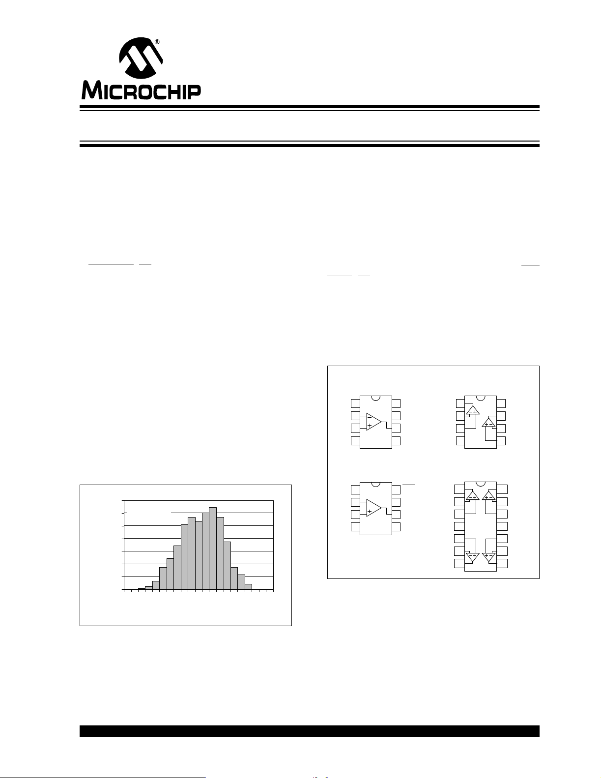
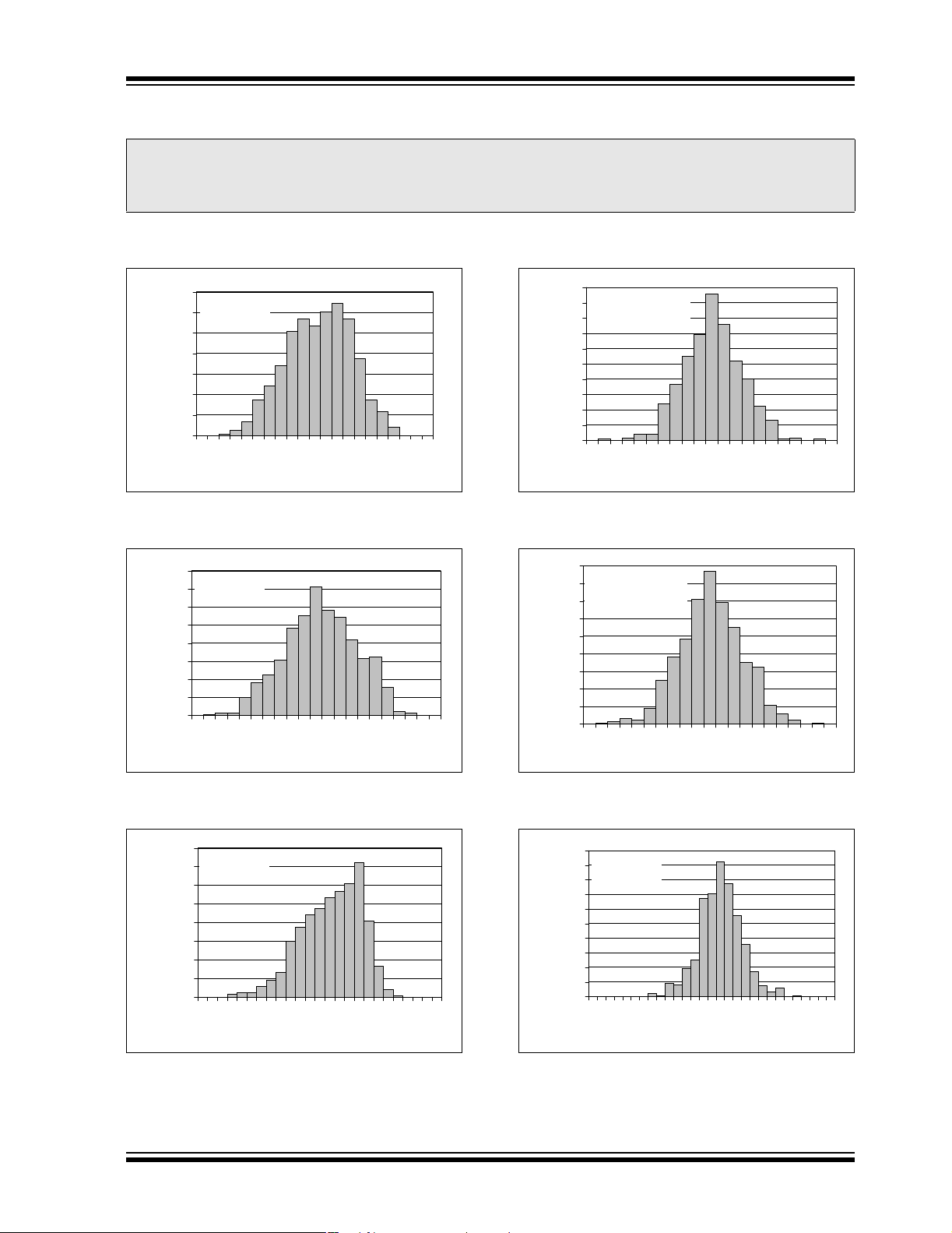
Input Offset Volt age
14%
598 Samples
Percentage of Occurrences
12%
10%
8%
6%
4%
2%
0%
V
-100
= 5.5V
DD
-80
-60
-40
Input Offset Voltage (µV)
0
20
40
60
-20
80
100
Description
The MCP616/7/8/9 family of operational amplifiers (op
amps) from Microchip Technology Inc. are capable of
precision, low-power, single-supply operation. These
op amps are unity-gain stable, have low input offset
voltage (±150 µV, max.), rail-to-rail output swing and
low input offset current (0.3 nA, typ.). These features
make this family of op amps well suited for batterypowered applications.
The single MCP616, the single MCP618 with Chip
Select (CS) and the dual MCP617 are all available in
standard 8-lead PD IP, SOIC and MSOP pac kages. The
quad MCP619 is offered in standard 14-lead PDIP,
SOIC and TSSOP packages. All devices are fully
specified from -40°C to +85°C, with power supplies
from 2.3V to 5.5V.
Package Types
MCP616
PDIP, SOIC, MSOP
NC
VIN–
VIN+
V
SS
1
2
3
4
8
7
6
5
MCP618
PDIP, SOIC, MSOP
NC
VIN–
VIN+
V
SS
1
2
3
4
8
7
6
5
NC
V
V
NC
CS
V
V
NC
DD
OUT
DD
OUT
V
V
V
V
OUTA
V
V
V
V
V
OUTB
MCP617
PDIP, SOIC, MSOP
OUTA
INA
INA
V
SS
1
2
–
3
+
4
8
7
6
5
MCP619
PDIP, SOIC, TSSOP
INA
INA
V
INB
INB
DD
1
2
–
3
+
4
5
+
6
–
7
14
13
12
11
10
9
8
V
V
V
V
V
V
V
V
V
V
V
DD
OUTB
INB
INB
OUTD
IND
IND
SS
INC
INC
OUTC
–
+
–
+
+
–
© 2005 Microchip Technology Inc. DS21613B-page 1
MCP616/7/8/9
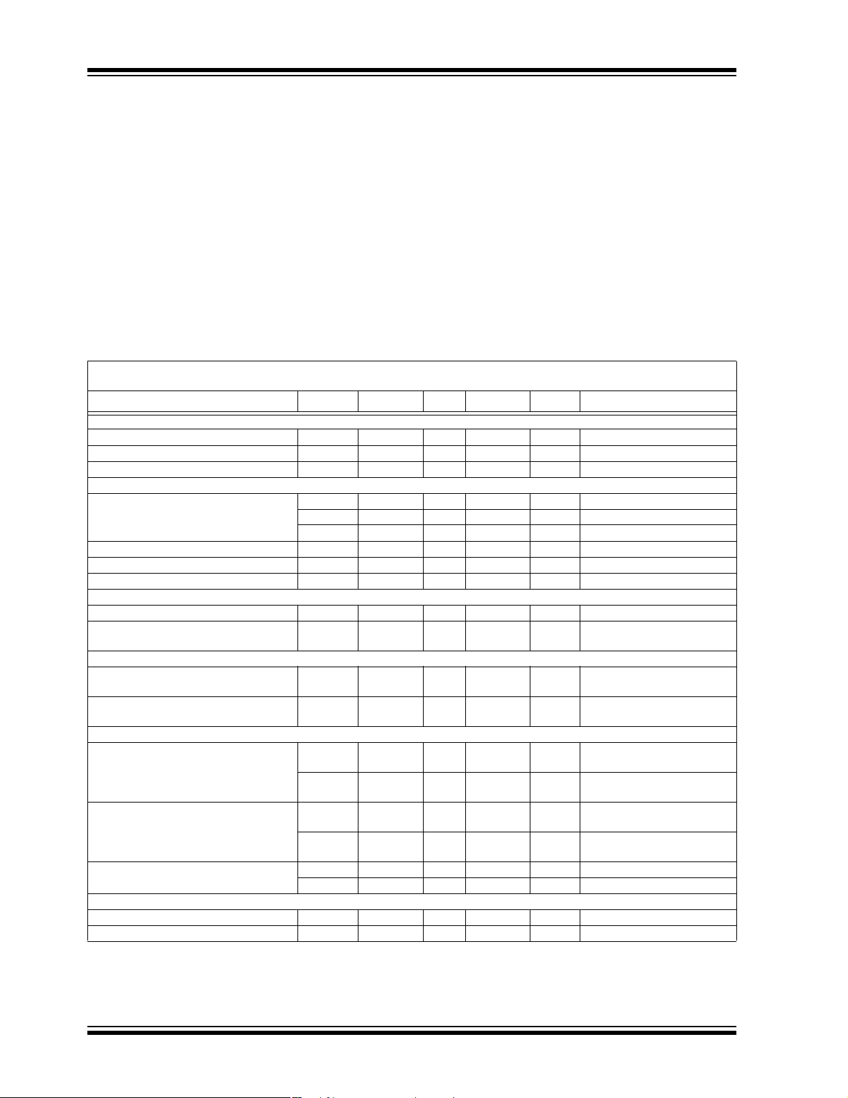
1.0 ELECTRICAL CHARACTERISTICS
† Notice: Stresses above those listed under “Absolute
Maximum Ratings” may cause permanent damage to the
device. This is a stress rating only and functional operation of
the device at those or any other conditions above those
Absolute Maximum Ratings †
indicated in the operational listings of this specification is not
implied. Exposure to maximum rating conditions for extended
VDD–VSS .......................................................................7.0V
All Inputs and Outputs ................... V
Difference Input Voltage ......................................|V
– 0.3V to VDD+0.3V
SS
DD–VSS
|
periods may affect device reliability.
Output Short Circuit Current .................................Continuous
Current at Input Pins ....................................................±2 mA
Current at Output and Supply Pins ............................±30 mA
Storage Temperature ....................................-65°C to +150°C
Maximum Junction Temperature (T
) .........................+150°C
J
ESD protection on all pins (HBM;MM) ...................4 kV; 200V
DC ELECTRICAL CHARACTERISTICS
Electrical Specifications: Unless otherwise indicated, VDD= +2.3V to +5.5V, VSS=GND, TA= 25°C, VCM=VDD/2, V
and R
= 100 kΩ to VDD/2.
L
Parameters Sym Min Typ Max Units Conditions
Input Offset
Input Offset Voltage V
Input Offset Drift with Temperature ΔV
OS
/ΔT
OS
Power Supply Rejection PSRR 86 105 — dB
Input Bias Current and Impeda nc e
Input Bias Current I
At Temperat ure I
At Temperature I
Input Offset Current I
Common Mode Input Impedance Z
Differential Input Impedance Z
B
B
B
OS
CM
DIFF
Common Mode
Common Mode Input Voltage Range V
CMR
Common Mode Rejection Ratio CMRR 80 100 — dB V
Open-Loop Gain
DC Open-Loop Gain (large signal) A
DC Open-Loop Gain (large signal) A
OL
OL
Output
Maximum Output Voltage Swing V
Linear Output Voltage Range V
Output Short Circuit Current I
, V
OL
V
, V
OL
OUT
V
OUT
SC
I
SC
Power Supply
Supply Voltage V
Quiescent Current per Amplifier I
DD
Q
–150 — +150 µV
— ±2.5 — µV/°C TA = -40°C to +85°C
A
-35 -15 -5 nA
-70 -21 — nA TA = -40°C
—-12— nAT
= +85°C
A
— ±0.15 — nA
— 600||4 — MΩ||pF
—3||2—MΩ||pF
V
SS
VDD–0.9 V
= 5.0V,
DD
= 0.0V to 4.1V
V
CM
100 120 — dB RL = 25 kΩ to VDD/2,
= 0.05V to VDD– 0.05V
V
OUT
95 115 — dB RL = 5 kΩ to VDD/2,
= 0.1V to VDD–0.1V
V
OUT
OHVSS
OHVSS
+15 — VDD–20 mV RL = 25 kΩ to VDD/2,
0.5V output overdrive
+45 — VDD–60 mV RL = 5 kΩ to VDD/2,
0.5V output overdrive
VSS+50 — VDD–50 mV RL = 25 kΩ to VDD/2,
A
≥ 100 dB
OL
VSS+ 100 — VDD– 100 mV RL = 5 kΩ to VDD/2,
≥ 95 dB
A
—±7—mAV
OL
DD
= 2.3V
—±17— mAVDD = 5.5V
2.3 — 5.5 V
12 19 25 µA IO = 0
OUT
≈ VDD/2
DS21613B-page 2 © 2005 Microchip Technology Inc.
MCP616/7/8/9
AC ELECTRICAL CHARACTERISTICS
Electrical Specifications: Unless otherwise indicated, VDD= +2.3V to +5.5V, VSS= GND, TA= 25°C, VCM=VDD/2, V
= 100 kΩ to VDD/2 and CL=60pF.
R
L
Parameters Sym Min Typ Max Units Conditions
AC Response
Gain Bandwidth Product GBWP — 190 — kHz
Phase Margin PM — 57 — ° G = +1
Slew Rate SR — 0.08 — V/µs
Noise
Input Noise Voltage E
Input Noise Voltage Density e
Input Noise Current Density i
ni
ni
ni
—2.2— µV
—32—nV/√Hz f = 1 kHz
—70— fA/√Hz f = 1 kHz
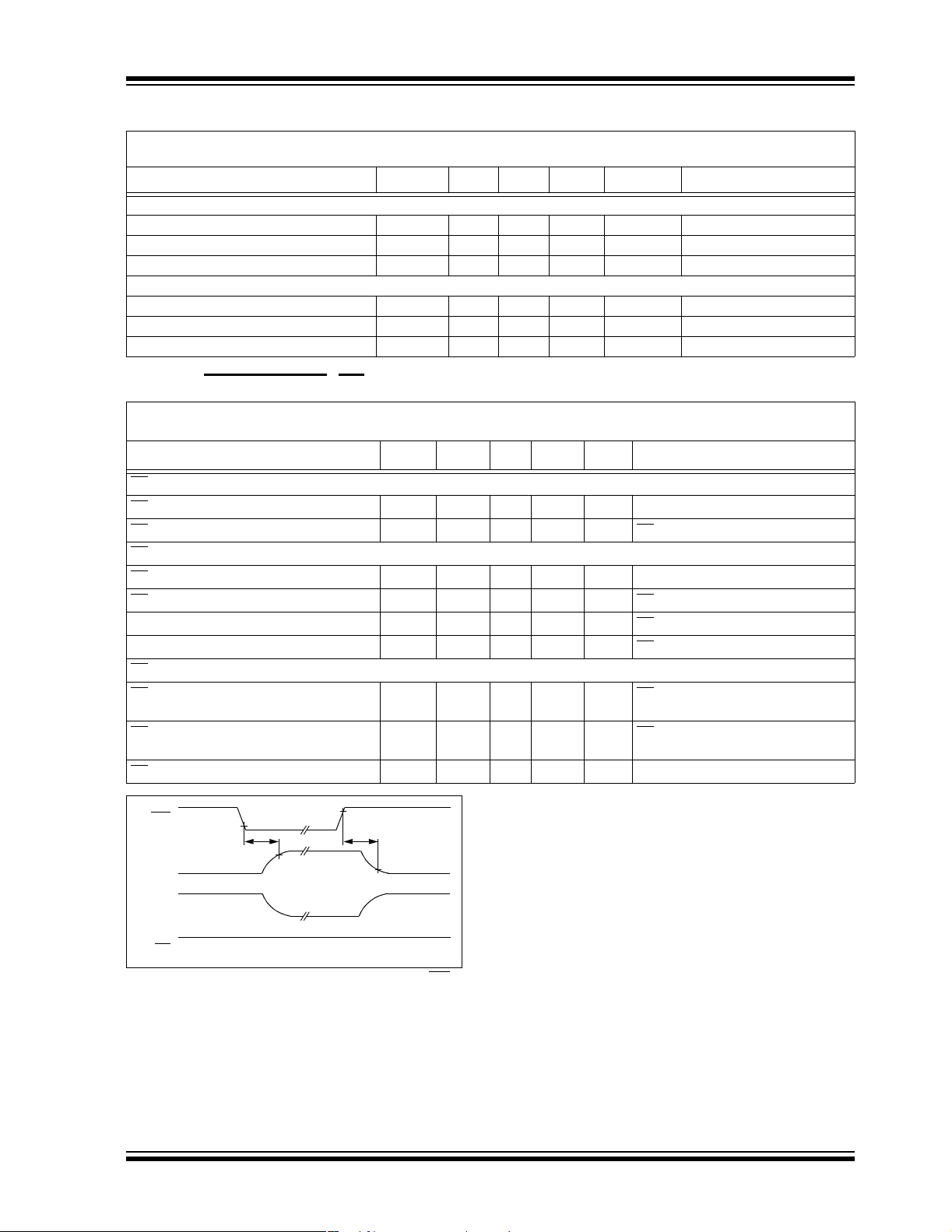
MCP618 CHIP SELECT (CS) ELECTRICAL CHARACTERISTICS
Electrical Specifications: Unless otherwise indicated, V
= 100 kΩ to VDD/2 and CL=60pF.
R
L
Parameters Sym Min Typ Max Units Conditions
CS Low Specifications
CS
Logic Threshold, Low V
CS
Input Current, Low I
CS High Specifications
CS
Logic Threshold, High V
CS
Input Current, High I
GND Current I
Amplifier Output Leakage I
CS Dynamic Specifications
CS
Low to Amplifier Output Turn-on Time t
CS High to Amplifier Output High-Z t
CS Hysteresis V
IL
CSL
IH
CSH
SS
O(LEAK)
ON
OFF
HYST
= +2.3V to +5.5V, VSS=GND, TA= 25°C, VCM=VDD/2, V
DD
V
—0.2VDDV
SS
–1.0 0.01 — µA CS = V
0.8 V
—VDDV
DD
—0.012 µACS = V
-2 -0.05 — µA CS = V
—10—nACS = V
— 9 100 µs CS = 0.2VDD to V
G = +1 V/V, R
—0.1— µsCS = 0.8VDD to V
G = +1 V/V, R
—0.6— VVDD = 5.0V
f = 0.1 Hz to 10 Hz
P-P
SS
DD
DD
DD
= 0.9(VDD/2),
OUT
= 1 kΩ to V
L
= 0.1(VDD/2),
OUT
= 1 kΩ to V
L
OUT
OUT
SS
SS
≈ VDD/2,
≈ VDD/2,
V
t
IL
ON
-19 µA (typ.)
CS
V
High-Z High-Z
OUT
-50 nA (typ.) -50 n A (typ.)
I
SS
I
10 nA (typ.) 10 nA (typ.)
CS
V
IH
t
OFF
FIGURE 1-1: Timing Diagram for the CS Pin on the MCP618.
© 2005 Microchip Technology Inc. DS21613B-page 3
MCP616/7/8/9
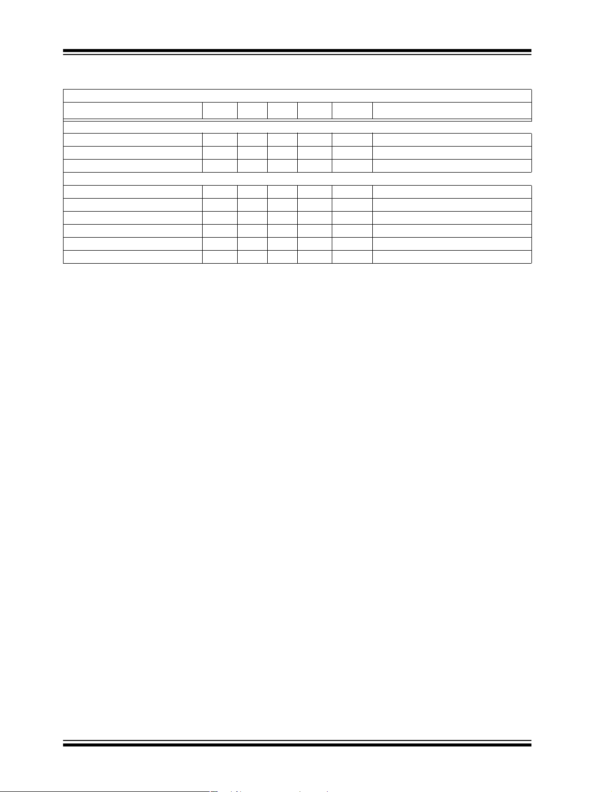
TEMPERATURE CHARACTERISTICS
Electrical Specifications: Unless otherwise indicated, VDD= +2.3V to +5.5V and VSS= GND.
Parameters Sym Min Typ Max Units Conditions
Temperature Ranges
Specified Temperature Range T
Operating Temperature Range T
Storage Temperature Range T
Thermal Package Resistances
Thermal Resistance, 8L-PDIP θ
Thermal Resistance, 8L-SOIC θ
Thermal Resistance, 8L-MSOP θ
Thermal Resistance, 14L-PDIP θ
Thermal Resistance, 14L-SOIC θ
Thermal Resistance, 14L-TSSOP θ
Note 1: The MCP616/7/8/9 operate over this extended temperature range, but with reduced performance. In any case, the
Junction Temperature (T
) must not exceed the Absolute Maximum specification of +150°C.
J
-40 — +85 °C
A
-40 — +125 °C Note 1
A
-65 — +150 °C
A
—85 — °C/W
JA
— 163 — °C/W
JA
— 206 — °C/W
JA
—70 — °C/W
JA
— 120 — °C/W
JA
— 100 — °C/W
JA
DS21613B-page 4 © 2005 Microchip Technology Inc.
MCP616/7/8/9
2.0 TYPICAL PERFORMANCE CURVES
Note: The graphs and tables p r ov ide d f oll ow in g th is no te a r e a s t ati sti ca l s um ma r y bas ed on a l im ite d n um ber of
samples and are provided for informational purposes only. The performance characteristics listed herein
are not tested or guaranteed. In some graphs or tables, the data presented may be outside the specified
operating range (e.g., outside specified power supply range) and therefore outside the warranted range.
Note: Unless otherwise indicated, VDD= +2.3V to +5.5V, VSS= GND, TA=25°C, VCM=VDD/2, V
=100kΩ to VDD/2 and CL=60pF.
R
L
14%
598 Samples
12%
10%
Percentage of Occurrences
8%
6%
4%
2%
0%
V
-100
= 5.5V
DD
-80
-60
-40
Input Offset Voltage (µV)
-20
0
20
40
60
80
FIGURE 2-1: Input Offset Voltage at
V
=5.5V.
DD
16%
598 Samples
14%
12%
10%
Percentage of Occurrences
8%
6%
4%
2%
0%
V
-100
= 2.3V
DD
-80
-60
0
-40
-20
Offset Voltage (µV)
20
40
60
100
80
100
20%
598 Samples
18%
16%
14%
12%
10%
Percentage of Occurrences
8%
6%
4%
2%
0%
V
DD
T
A
-10
= 5.5V
= -40°C to +85°C
-8
-6
-4
-2
Input Offset Voltage Drift (µV/°C)
FIGURE 2-4: Input Offset Voltage Drift at
V
=5.5V.
DD
18%
598 Samples
16%
14%
12%
10%
Percentage of Occurrences
8%
6%
4%
2%
0%
V
DD
T
A
-10
= 2.3V
= -40°C to +85°C
-8
-6
-4
Input Offset Voltage Drift (µV/°C)
0
-2
0
OUT
2
2
≈ VDD/2,
4
6
4
6
8
10
8
10
FIGURE 2-2: Input Offset Voltage at
=2.3V.
V
DD
16%
600 Samples
14%
12%
10%
Percentage of Occurrences
8%
6%
4%
2%
0%
V
DD
-22
= 5.5V
-21
-20
-19
-18
Input Bias Current (nA)
-17
-16
-15
-14
-13
-12
FIGURE 2-3: Input Bias Current at
=5.5V.
V
DD
-11
-10
FIGURE 2-5: Input Offset Voltage Drift at
=2.3V.
V
DD
20%
600 Samples
18%
16%
14%
12%
10%
Percentage of Occurrences
8%
6%
4%
2%
0%
V
-0.7
= 5.5V
DD
-0.6
-0.5
-0.4
-0.3
-0.2
Input Offset Current (nA)
-0.1
0.0
0.1
0.2
0.3
0.4
0.5
0.6
0.7
FIGURE 2-6: Input Offset Current at
=5.5V.
V
DD
© 2005 Microchip Technology Inc. DS21613B-page 5
MCP616/7/8/9
0
0
0
Note: Unless otherwise indicated, VDD= +2.3V to +5.5V, VSS= GND, TA=25°C, VCM=VDD/2, V
=100kΩ to VDD/2 and CL=60pF.
R
L
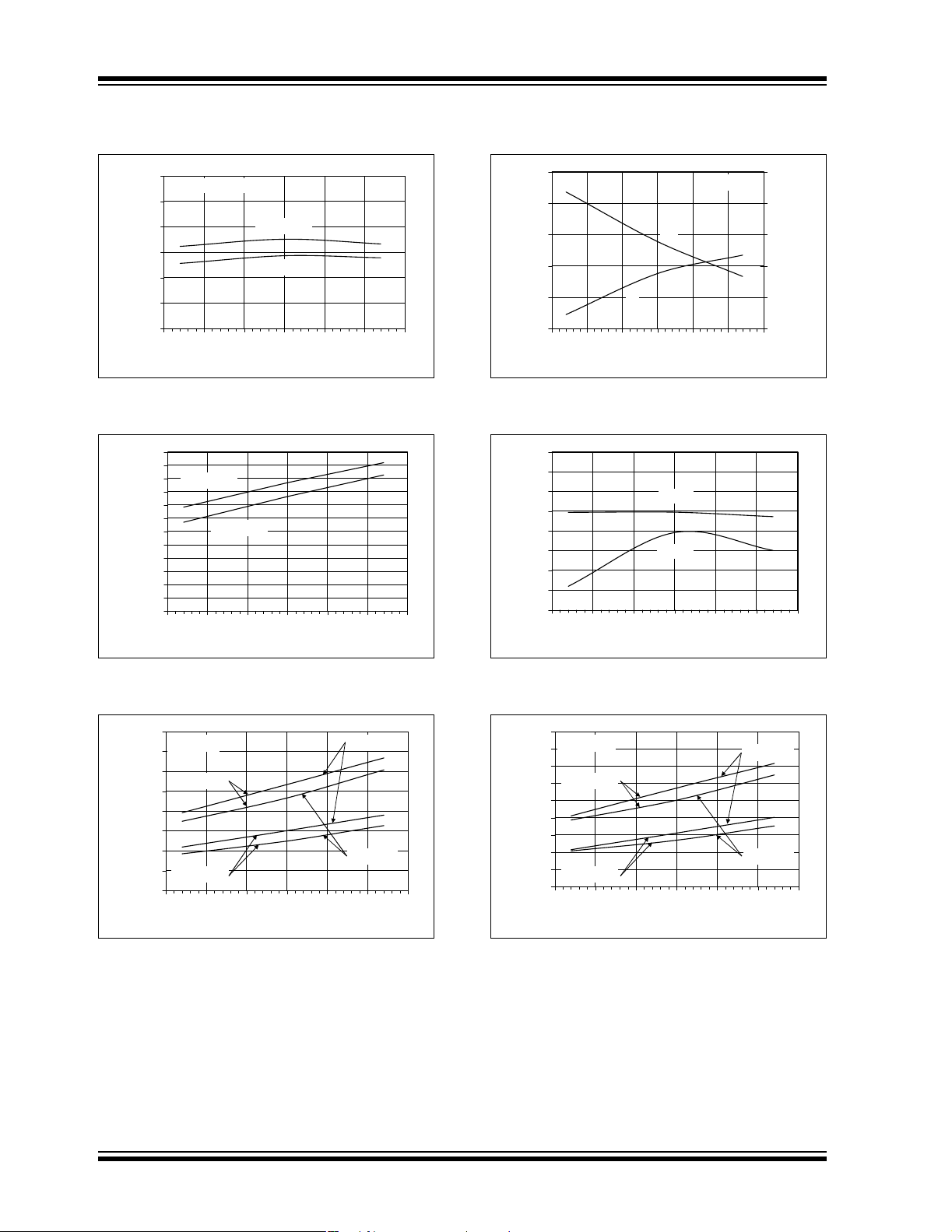
150
Representative Part
100
50
0
-50
-100
Input Offset Voltage (µV)
-150
-50 -25 0 25 50 75 100
VDD = 5.5V
VDD = 2.3V
Ambient Temperature (°C)
FIGURE 2-7: Input Offset Voltage vs. Ambient Temperature.
24
22
20
VDD = 5.5V
18
16
14
12
10
8
(µA/Amplifier)
6
Quiescent Current
4
2
0
-50-250 25507510
VDD = 2.3V
Ambient Temperature (°C)
FIGURE 2-10: Input Bias, Offset Currents vs. Ambient Temperature.
0
-5
I
-10
-15
-20
Input Bias Current (nA)
-25
-50 -25 0 25 50 75 100
120
115
110
105
100
95
90
CMRR, PSRR (dB)
85
80
-50-250 255075100
Ambient Temperature (°C)
Ambient Temperature (°C)
OS
I
B
PSRR
CMRR
≈ VDD/2,
OUT
VDD = 5.5V
1.0
0.8
0.6
0.4
0.2
0.0
Input Offset Current (nA)
FIGURE 2-8: Quiescent Current vs. Ambient Temperature.
40
RL = 5 k
35
30
25
20
(mV)
15
10
5
Output Voltage Headroom
0
-50-250 25507510
Ω
VDD = 5.5V
VDD = 2.3V
Ambient Temperature (°C)
VDD – V
VOL – V
OH
SS
FIGURE 2-9: Maximum Output Voltage
Swing vs. Ambient Temperature at R
=5kΩ.
L
FIGURE 2-11: CMRR, PSRR vs. Ambient Temperature.
9
RL = 25 kΩ
8
7
VDD = 5.5V
6
5
4
(mV)
3
2
1
VDD = 2.3V
Output Voltage Headroom
0
-50 -25 0 25 50 75 10
Ambient Temperature (°C)
VDD – V
VOL – V
OH
SS
FIGURE 2-12: Maximum Output Voltage
Swing vs. Ambient Temperature at RL=25kΩ.
DS21613B-page 6 © 2005 Microchip Technology Inc.
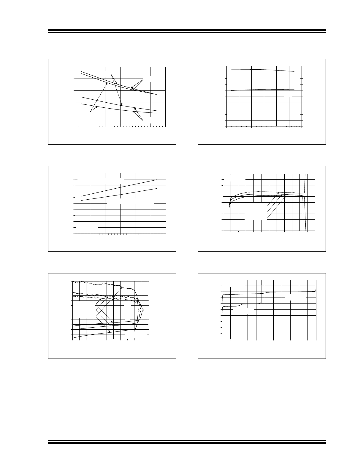
MCP616/7/8/9
0
0
OSIB
5
Note: Unless otherwise indicated, VDD= +2.3V to +5.5V, VSS= GND, TA=25°C, VCM=VDD/2, V
=100kΩ to VDD/2 and CL=60pF.
R
L
25
I
20
15
(mA)
10
| I
|
SC–
5
Output Short Circuit Current
0
-50-250 25507510
SC+
Ambient Temperature (°C)
VDD = 5.5V
VDD = 2.3V
FIGURE 2-13: Output Short Circuit Current vs. Ambie nt Temperature.
0.10
0.09
Low-to-High Transition
0.08
0.07
0.06
0.05
0.04
0.03
Slew Rate (V/µs)
0.02
0.01
VDD = 5.0V
0.00
-50 -25 0 25 50 75 10
High-to-Low Transition
Ambient Temperature (°C)
FIGURE 2-16: Gain Bandwidth Product, Phase Margin vs. Ambient Temperature.
200
180
GBWP
160
140
120
100
(kHz)
80
60
40
Gain Bandwidth Product
20
0
-50 -25 0 25 50 75 100
Ambient Temperature (°C)
100
VDD = 5.5V
80
60
40
20
Input Offset Voltage (µV)
0
-20
-40
-60
-80
-100
-0.5
TA = +85°C
T
= +25°C
A
T
= -40°C
A
0.0
0.5
1.0
1.5
2.0
Common Mode Input Voltage (V)
2.5
OUT
3.0
≈ VDD/2,
PM
3.5
4.0
4.5
100
90
80
70
60
50
40
30
20
10
0
5.0
Phase Margin (°)
5.5
FIGURE 2-14: Slew Rate vs. Ambient Temperature.
Input Bias Current (nA)
30
25
20
15
10
TA = +85°C
5
T
= +25°C
0
A
T
= -40°C
-5
A
-10
-15
-20
-25
-30
0.0
0.5
1.0
1.5
Common Mode Input Voltage (V)
2.0
2.5
3.0
I
VDD = 5.5V
3.5
4.0
4.5
5.0
0.30
0.25
0.20
0.15
0.10
0.05
0.00
-0.05
-0.10
-0.15
-0.20
-0.25
-0.30
5.5
Input Offset Current (nA)
FIGURE 2-15: Input Bias, Offset Currents vs. Common Mode Input Voltage.
FIGURE 2-17: Input Offset Voltage vs. Common Mode Input Voltage.
50
RL = 25 k
40
30
20
10
0
-10
-20
-30
Input Offset Voltage (µV)
-40
-50
0.0 0.5 1.0 1.5 2.0 2.5 3.0 3.5 4.0 4.5 5.0 5.
Ω
VDD = 5.5V
VDD = 2.3V
Output Voltage (V)
FIGURE 2-18: Input Offset Voltage vs. Output Voltage.
© 2005 Microchip Technology Inc. DS21613B-page 7
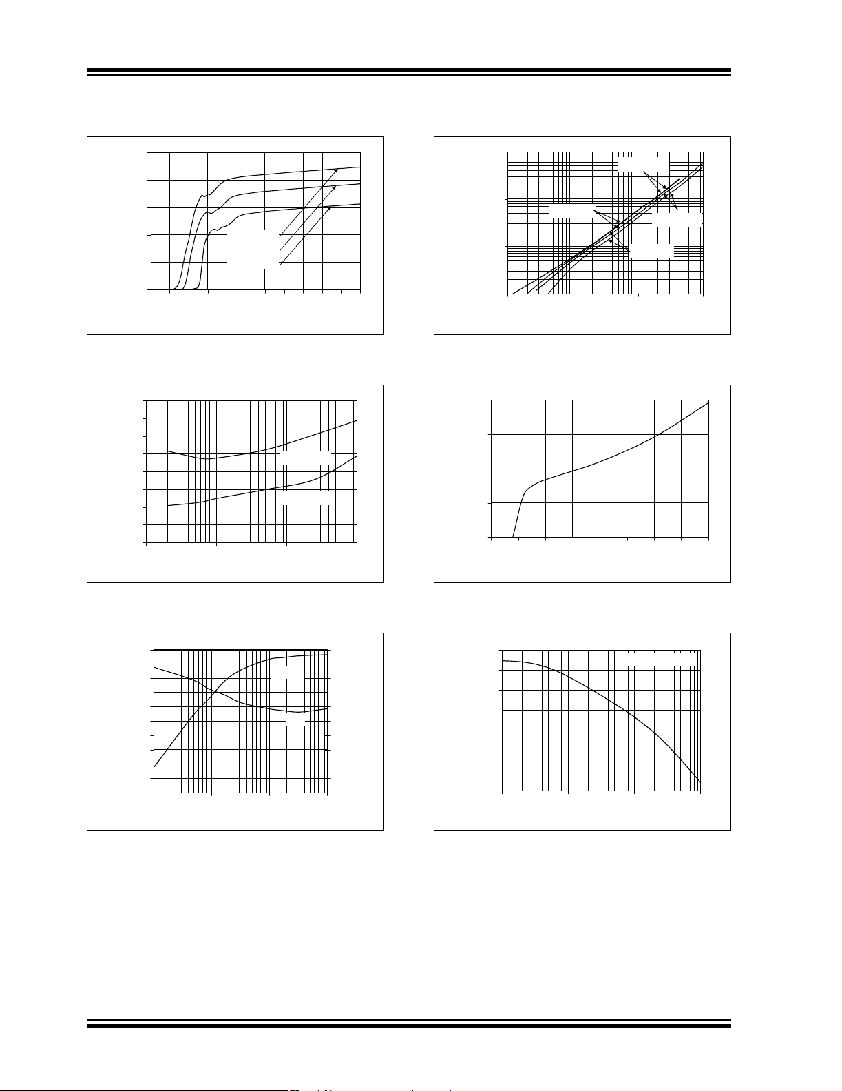
MCP616/7/8/9
5
k
Gain Bandwidth Product
5
5
Note: Unless otherwise indicated, VDD= +2.3V to +5.5V, VSS= GND, TA=25°C, VCM=VDD/2, V
=100kΩ to VDD/2 and CL=60pF.
R
L
25
20
15
10
(µA/Amplifier)
Quiescent Current
5
0
0.0 0.5 1.0 1.5 2.0 2.5 3.0 3.5 4.0 4.5 5.0 5.
TA = +85°C
T
= +25°C
A
T
= -40°C
A
Power Supply Voltage (V)
FIGURE 2-19: Quiescent Current vs. Power Supply Voltage.
130
125
120
115
110
105
100
95
DC Open-Loop Gain (dB)
90
100 1k 10k 100
0.1 1 10 100
Load Resistance (
VDD = 5.5V
VDD = 2.3V
Ω)
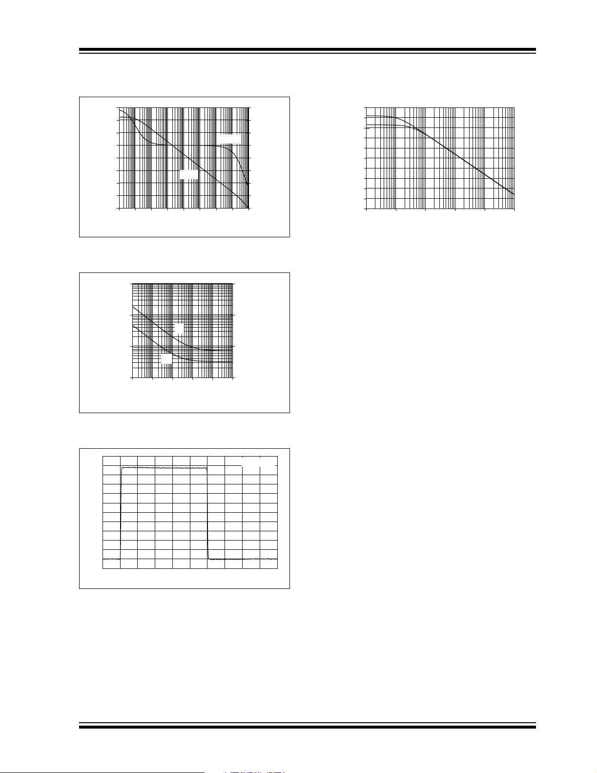
FIGURE 2-22: Output Voltage Headroom vs. Output Current Magnitude.
1,000
100
10
Output Voltage Headroom (mV)
1
10µ 100µ 1m 10m
0.01 0.1 1 10
125
RL = 25 kΩ
120
115
110
DC Open-Loop Gain (dB)
105
1.5 2.0 2.5 3.0 3.5 4.0 4.5 5.0 5.
VDD – V
OH
Output Current Magnitude (A)
Power Supply Voltage (V)
≈ VDD/2,
OUT
VDD = 2.3V
VDD = 5.5V
VOL – V
SS
FIGURE 2-20: DC Open-Loop Gain vs. Load Resistance.
200
180
160
140
120
100
(kHz)
80
60
40
20
0
1k 10k 100k 1M
1 10 100 1,000
Load Resistance (
GBWP
PM
Ω)
100
90
80
70
60
50
40
30
20
10
0
FIGURE 2-21: Gain-Bandwidth Product, Phase Margin vs. Load Resistance.
Phase Margin (°)
FIGURE 2-23: DC Open-Loop Gain vs. Power Supply Voltage.
140
130
120
110
100
90
Seperation (dB)
Channel-to-Channel
80
70
100 100k10k1k
1.E+02 1.E+03 1.E+04 1.E+0
Frequency (Hz)
Referred to Input
FIGURE 2-24: Channel-to-Channel Separation vs. Frequency (MCP617 and MCP619 only).
DS21613B-page 8 © 2005 Microchip Technology Inc.
MCP616/7/8/9
Note: Unless otherwise indicated, VDD= +2.3V to +5.5V, VSS= GND, TA=25°C, VCM=VDD/2, V
=100kΩ to VDD/2 and CL=60pF.
R
L
140
120
100
80
60
40
20
Open-Loop Gain (dB)
0
-20
0.01 0.1 1 10 100 1k 10k 100k 1M
1.E-021.E-011.E+001.E+011.E+021.E+031.E+041.E+051.E+
Gain
Phase
FIGURE 2-25: Open-Loop Gain, Phase vs. Frequency.
10,000
Hz)
1,000
i
ni
100
Density (nV/
Input Noise Voltage
e
ni
06Frequency (Hz)
10,000
1,000
100
0
-30
-60
-90
-120
-150
-180
Open-Loop Phase (°)
-210
-240
Hz)
Density (fA/
Input Noise Current
FIGURE 2-28: CMRR, PSRR vs. Frequency.
OUT
≈ VDD/2,
10
0.1 101 100 10k1k
1.E-011.E+001.E+011.E+021.E+031.E+0
Frequency (Hz)
10
4
FIGURE 2-26: Input Noise Voltage, Current Densities vs. Frequency.
Gain = +1
Output Voltage (20 mV/div)
Time (50 µs/div)
FIGURE 2-27: Small-Signal, Non-Inverting Pulse Response.
FIGURE 2-29: Maximum Output Voltage Swing vs. Frequency.
FIGURE 2-30: Small-Signal, Inverting Pulse Response.
© 2005 Microchip Technology Inc. DS21613B-page 9

MCP616/7/8/9
Note: Unless otherwise indicated, VDD= +2.3V to +5.5V, VSS= GND, TA=25°C, VCM=VDD/2, V
=100kΩ to VDD/2 and CL=60pF.
R
L
5
4
3
2
Output Voltage (V)
1
0
Time (50 µs/div)
Gain = +1
= 5.0V
V
DD
FIGURE 2-31: Large-Signal, Non-Inverting Pulse Response.
5.0
4.5
4.0
3.5
3.0
2.5
2.0
1.5
Output Voltage (V)
1.0
0.5
0.0
VDD = 5.0V
Gain = +1 V/V
= 1 kΩ to V
R
L
Output
High-Z
SS
Output
On
Time (5 µs/div)
CS
V
OUT
Output
High-Z
10
5
0
-5
-10
-15
-20
-25
-30
-35
-40
Chip Select Voltage (V)
5.0
4.5
4.0
3.5
3.0
2.5
2.0
1.5
Output Voltage (V)
1.0
0.5
0.0
Gain = -1
V
= 5.0V
DD
Time (50 µs/div)
FIGURE 2-34: Large-Signal, Inverting Pulse Response.
5.0
4.5
4.0
3.5
Output
3.0
On
2.5
2.0
1.5
1.0
0.5
Internal CS Switch Output (V)
0.0
CS swept
High-to-Low
0.0 0.5 1.0 1.5 2.0 2.5 3.0 3.5 4.0 4.5 5.0
Hysteresis
Chip Select Voltage (V)
≈ VDD/2,
OUT
CS swept
Low-to-High
VDD = 5.0V
Output
High-Z
FIGURE 2-32: Chip Select (CS) to Amplifier Output Response Time (MCP618 only).
6
5
4
3
2
1
0
Input, Output Voltages (V)
-1
V
OUT
Time (100 µs/div)
Gain = +2 V/V
V
V
IN
= 5.0V
DD
FIGURE 2-33: The MCP616/7/8/9 Show No Phase Reversal.
FIGURE 2-35: Chip Select (CS) Internal Hysteresis (MCP618 only).
DS21613B-page 10 © 2005 Microchip Technology Inc.

MCP616/7/8/9
3.0 PIN DESCRIPTIONS
Descriptions of the pins are listed in Table 3-1.
TABLE 3-1: PIN FUNCTION TABLE
MCP616 MCP617 MCP618 MCP619 Symbol Description
6161V
2222V
3333V
7874 V
—5—5 V
—6—6 V
—7—7 V
——— 8 V
——— 9 V
———10 V
44411 V
———12 V
———13 V
———14V
—— 8 — CS
, V
OUT
OUTA
–, V
IN
INA
+, V
IN
INA
DD
+ Non-inverting Input (op amp B)
INB
– Inverting Input (op amp B)
INB
OUTB
OUTC
– Inverting Input (op amp C)
INC
+ Non-inverting Input (op amp C)
INC
SS
+ Non-inverting Input (op amp D)
IND
– Inverting Input (op amp D)
IND
OUTD
Output (op amp A)
– Inverting Input (op amp A)
+ Non-inverting Input (op amp A)
Positive Power Supply
Output (op amp B)
Output (op amp B)
Negative Power Supply
Output (op amp D)
Chip Select
1, 5, 8 — 1, 5 — NC No Internal Connection
3.1 Analog Outputs
The output pins are low-impedance voltage sources.
3.4 Power Supply (VSS and VDD)
The positive powe r s upp ly (VDD) is 2.5V to 5.5V h igh er
than the negative power supply (V
3.2 Analog Inputs
The non-inverting and inverting inputs are highimpedance PNP inputs with low bias currents.
3.3 Chip Select Digital Input (CS )
This is a CMOS, Schmitt-tri ggered inpu t that places th e
MCP618 op amp into a low-power mode of operation.
operation, the other pins are between V
Typically, these parts are used in a single-supply
(positive) configuration. In this case, VSS is connected
to ground and V
is connected to the supply. VDD will
DD
need a local bypass capacitor (typically 0.01 µF to
0.1 µF) within 2 mm of the V
use a bulk capacitor (typically 1 µF or larger) within
100 mm of the V
pin; it can be shared with nearby
DD
analog parts.
). For normal
SS
and VDD.
SS
pin. These parts sh ould
DD
© 2005 Microchip Technology Inc. DS21613B-page 11

MCP616/7/8/9
4.0 APPLICATIONS INFORMATION
The MCP616/7/8/9 family of op amps is manufactured
using Microchip’s state-of-the-art CMOS process,
which includes PNP transistors. These op amps are
unity-gain stable and suitable for a wide range of
general purpose applications .
4.1 Inputs
The MCP616/7/8/9 op amps are designed to prevent
phase reversal when the input pins exceed the supply
voltages. Figure 2-33 shows the input voltage
exceeding the su ppl y v ol t age w ith out any pha se reversal.
The inputs of the MCP616/7/8/9 op amps connect to a
differential PN P in p ut stag e . T he Comm on Mo de Inpu t
Voltage Range (V
supply systems (V
means that the amp li fier i np ut be ha ves li nearly as long
as the Common Mode Input Voltage (VCM) is kept
within the specified limits (V
Input voltages that exceed the Absolute Maximum
Voltage Range (V
excessive current to flow into or out of the input pins.
Current beyond ±2 mA can cause reliability problems.
Applications that exceed this rating must be externally
limited with a resistor, as shown in Figure 4-1.
R
V
IN
Maximum expected V
()VDD–
------------------------------------------------------------------------------
R
≥
IN
V
---------------------------------------------------------------------------
R
≥
IN
FIGURE 4-1: Input Current-Limiting
Resistor (R
IN
).
) includes ground in single-
CMR
), but does not include VDD. This
SS
to VDD– 0.9V at +25°C).
SS
– 0.3V to VDD+ 0.3V) can cause
SS
IN
V
OUT
MCP61X
IN
2 mA
Minimum expected V
()–
SS
IN
2 mA
4.2 DC Offsets
The MCP616/7/8/9 f amily of o p amps have a PNP i nput
differential pair that gives good DC performance. They
have very low input offset voltage (±150 µV, max.) at
= +25°C, with a typical bias current of -15 nA
T
A
(sourced out of the inputs).
There must be a DC path to ground (or power supply)
from both inputs, or the op amp will not bias properly.
V
V
OUT
OUT
||R
1
The DC resistanc es see n by the o p amp inp uts (R
and R4||R5 in Figure 4-2) need to be equal and less
than 100 kΩ, to minimize the total DC offset.
R
V
1
1
C
R
3
3
R
2
MCP61X
V
2
R
4
R
5
FIGURE 4-2: Example Circuit for Calculating DC Offset.
To calculate the DC bias point and DC offset, convert
the circuit to its DC equivalent:
• Replace capacito rs wi th ope n circuits
• Replace inductors with short circuits
• Replace AC voltage sources with short circuits
• Replace AC current sources with open circuits
• Convert DC sources and resistances into their
Thevenin equivalent form
The DC equivalent circuit for Figure 4-2 is shown in
Figure 4-3.
R
V
1
V
EQ
1
R
EQ
R
2
MCP61X
2
R
5
V
EQV2
R
EQ
------------------
⋅=
R4R5+
R4 || R
=
5
FIGURE 4-3: Equivalent DC Circuit.
DS21613B-page 12 © 2005 Microchip Technology Inc.

MCP616/7/8/9
:
Now calculate the nominal DC bias point with offset:
EQUATION 4-1:
GN1R2R1⁄+=
V
= GN [VOS + IB ((R1 ||R2 ) – REQ )
OOS
((R1 ||R2 ) + REQ ) / 2]
– I
OS
VCM = VEQ – (IB + IOS /2) R
V
= VEQ (GN ) – V1 (GN – 1) + V
OUT
EQ
OOS
Where:
= op amp’s noise gain (from the
G
N
non-inverting input to the output)
V
= circuit’s output offset voltage
OOS
= op amp’s input offset voltage
V
OS
I
= op amp’s input bias current
B
= op amp’s input offset current
I
OS
= op amp’s common mode input
V
CM
voltage
Use the worst-case specs and source values to
determine the worst-case
offset
for your design. Make sure the common mode
output voltage range and
input voltage range and output voltage range are not
exceeded.
4.3 Rail-to-Rail Output
There are two specifications that describe the output
swing capability of the MCP616/7/8/9 family of op
amps. The first specification (Maximum Output Voltage
Swing) defines the absolute maximum swing that can
be achieved under the specified load conditions. For
instance, the output voltage swings to within 15 mV of
the negative rail with a 25 kΩ load tied to V
DD
/2.
Figure 2-33 shows how the output voltage is limited
when the input goes beyond the linear region of
operation.
The second specification that describes the output
swing capabilit y of these amplifie rs is the Linear Outp ut
Voltage Range. This specification defines the
maximum output swing that can be achieved while the
amplifier still operates in its linear region. To verify
linear operation in this range, the large-signal DC
Open-Loop Gain (A
) is measured at point s inside the
OL
supply rails. Th e measurement must meet the specified
conditions in the specific ati on t able.
A
OL
4.4 Capacitive Loads
response. A unity-gain buffer (G = +1) is the most
sensitive to cap acit ive l oads, th ough al l gain s show th e
same general behavior.
When driving large capacitive loads with these op
amps (e.g., > 60 pF when G= +1), a small series
resistor at the output (R
in Figure 4-4) improves the
ISO
feedback loop’s phase margin (stability) by making the
output load resistive at higher frequencies. The
bandwidth will be generally lower than the bandwidth
with no capac itive load.
R
ISO
MCP61X
V
IN
C
L
FIGURE 4-4: Output Resistor, R
V
ISO
OUT
stabiliz es large capacitive loads.
Figure 4-5 gives recommended R
different capacitive loads and gains. The x-axis is the
normalized load capacitance (CL/GN), where GN is the
circuit’s nois e gain. For non -inverting ga ins, G
Signal Gain are equal. For inverting gains, G
1+|Signal Gain| (e.g., -1 V/V give s G
10,000
10k
)
(
ISO
1k
1,000
GN = +1
G
t +2
N
Recommended R
100
100
10p 1n
1.E-11 1.E-10 1.E-09 1.E-08
Normalized Load Capacitance; C
100p
FIGURE 4-5: Recommended R
values for
ISO
=+2V/V).
N
L/GN
ISO
and the
N
10n
(F)
Values
is
N
for Capacitive Loads.
After selecting R
resulting frequency response peaking and step
response overshoot. Modify R
response is reasonable. Bench evaluation and
simulations with the MCP616/7/8/9 SPICE macro
model are helpful.
for your circuit, double-check the
ISO
’s value until the
ISO
Driving large capacitive loads can cause stability
problems for voltage feedback op amps. As the load
capacitance increases, the feedback loop’s phase
margin decreases and the closed-loop bandwidth is
reduced. This produces gain peaking in the frequency
response, with overshoot and ringing in the step
© 2005 Microchip Technology Inc. DS21613B-page 13

MCP616/7/8/9
4.5 MCP618 Chip Select (CS)
The MCP618 is a single op am p with C hip Sel ect (CS).
When CS
50 nA (typ.) and flows through the CS
this happens, the amplifier output is put into a highimpedance state. By pulling CS low, the amplifier is
enabled. If the CS
not operate properly. Figure 1-1 shows the output
voltage and supply current response to a CS pulse.
is pulled high, the supply c urrent drops to
pin to VSS. When
pin is left floating, the amplifier may
4.6 Supply Bypass
With this family of operational amplifiers, the power
supply pin (V
bypass capacitor (i.e., 0.01 µF to 0.1 µF) within 2 mm
for good high-freque ncy performanc e. It may use a bulk
capacitor (i.e., 1 µF or larger) within 100 mm to provide
large, slow currents. This bulk capacitor is not required
and can be shared with other analog parts.
for single supply) should have a local
DD
4.7 Unused Op Amps
An unused op amp in a quad package (MCP619)
should be configured as shown in Figure 4-6. Both
circuits prevent the output from toggling and causing
crosstalk. Circuit A can use any reference voltage
between the supplies, provides a buffered DC voltage
and minimizes the supply current draw of the unused
op amp. Circuit B minimizes the number of
components, but may draw a little more supply current
for the unused op amp.
¼ MCP619 (A) ¼ MCP619 (B)
V
DD
V
DD
V
DD
4.8 PCB Surface Leakage
In applications where low input bias current is critical,
Printed Circuit Board (PCB) surface leakage effects
need to be considered. Surface leakage is caused by
humidity, dust or other contamination on the board.
Under low humidity conditions, a typical resistance
between nearby traces is 1 0
cause 5 pA of current to flow, which is greater than the
MCP616/7/8/9 family’s bias current at 25°C (1 pA,
typ.).
The easiest way to reduce surface leakage is to use a
guard ring around se nsi tiv e p ins (or t race s). The gua rd
ring is biased at the same voltage as the sensitive pin.
An example is shown below in Figure 4-7.
Guard Ring VIN–VIN+ V
FIGURE 4-7: Example Guard Ring Layout for Inverting Gain.
1. Non-inverting Gain and Unity Gain Buffer:
a) Connect the non-inverting pin (V
input with a wire that does not touch the
PCB surface.
b) Connect the guard ring to the invert ing input
pin (V
common mode input voltage.
2. Inverting Gain and Transimpedance gain (convert current to voltag e, such as photo de tectors )
amplifiers:
a) Connect the guard ring to the non-inverting
input pin (V
to the same reference voltage as the op
amp (e.g., V
b) Connect the inverting pin (VIN–) to the input
with a wire that does not touch the PCB
surface.
–). This biases the g uard rin g t o th e
IN
12
Ω. A 5V dif ference would
SS
+) to the
IN
+). This bi ases the gua rd ri ng
IN
/2 or ground).
DD
FIGURE 4-6: Unused Op Amps.
DS21613B-page 14 © 2005 Microchip Technology Inc.

MCP616/7/8/9
4.9 Application Circuits
4.9.1 HIGH GAIN PRE-AMPLIFIER
The MCP616/7/8/9 op amps are well suited to
amplifying small signals produced by low-impedance
sources/sensors. The low offset voltage, low offset
current and low noise fit well in this role. Figure 4-8
shows a typical pre-amplifier connected to a lowimpedance source (V
R
V
S
S
10 kΩ
VDD/2
FIGURE 4-8: High Gain Pre-amplifier.
For the best noise and offset performance, the source
resistance R
needs to be less than 15 kΩ. The DC
S
resistances at the inputs are equal to minimize the
offset voltage caused by the input bias currents
(Section 4.2 “DC Offsets”). In this circuit, the DC gai n
is 10 V/V, which wi ll give a typ ical band widt h of 19 kHz.
4.9.2 TWO OP AMP INSTR UMENTATION
AMPLIFIER
The two-op amp instrumentation amplifier shown in
Figure 4-9 serves the function of taking the difference
of two input voltages, level-shifting it and gaining it to
the output. This confi guration i s best sui ted for hig her
gains (i.e., gain > 3 V/V). The reference voltag e (V
is typically at mid-supply (V
environment.
V
OUT
R
V
REF
1
and RS).
S
MCP616
R
G
R
F
11.0 kΩ 100 kΩ
/2) in a single-supply
DD
R
V1V2–()1
R
R
2
⎛⎞
⎜⎟
⎝⎠
G
2R
1
1
------
--------- -++
R
R
2
G
R
R
2
V
OUT
REF
V
+=
REF
1
V
OUT
4.9.3 THREE OP AMP
INSTRUMENTATION AMPLIFIER
A classic, three-op amp instrumentation amplifier is
illustrated in Figure4-10. The two-input op amps
provide differential signal gain and a common mode
gain of +1. The output o p am p i s a d ifference amplifier,
which converts its input signal from differential to a
single-ended ou tput; it reje cts com mon mode signals at
its input. The ga in of th i s ci rcu it is sim p ly adj u ste d w ith
one resistor (R
). The reference voltage (V
G
typically referenced to mid-supply (V
/2) in single-
DD
REF
) is
supply applications.
V
OUT
V1V2–()1
⎛⎞
⎜⎟
⎝⎠
⎛⎞
4
2
------
---------+
R
G
⎜⎟
R
⎝⎠
3
V
+=
REF
R
2R
½
V
2
V
1
MCP617
R
2
R
G
R
2
MCP617
R
R
3
4
V
OUT
MCP616
V
R
R
3
4
REF
½
FIGURE 4-10: Three-Op Amp
)
Instrumentation Amplifier.
4.9.4 PRECISION GAIN WITH GOOD
LOAD ISOLATION
In Figure 4-11, the MCP6 16 op amp, R1 and R2 provide
a high gain to the input signal (V
offset voltage makes this an accurate circuit.
The MCP606 is configured as a unity-gain buffer. It
isolates the MCP616’ s o utput fr om the load, i ncreas ing
the high gain stag e’ s precisi on. Sinc e the MCP60 6 has
a higher output current, and the two amplifiers are
housed in sep a rate p ackages, there is m in im al change
in the MCP616’s offset voltage due to loading effect.
). The MCP616’s low
IN
V
2
V
1
FIGURE 4-9: Two-Op Amp Instrumentation Amplifier.
½
MCP617
½
MCP617
V
OUT
V
IN
VIN1R2R
MCP616
+()=
⁄
1
MCP606
V
OUT
The key specifications that make the MCP616/7/8/9
family appropriate for this application circuit are low
R
R
1
2
input bias current, low of fset volt age and hig h commonmode rejection.
FIGURE 4-11: Precision Gain with Good Load Isolation.
© 2005 Microchip Technology Inc. DS21613B-page 15

MCP616/7/8/9
5.0 DESIGN TOOLS
Microchip provides the basic design tools needed for
the MCP616/7/8/9 family of op amps.
5.1 SPICE Macro Model
The latest SPICE macro model for the MCP616/7/8/9
op amps is available on Microchip’s web site at
www.microchip.com. This model is intended to be an
initial design tool that works well in the op amp’s linear
region of operation at room temperature. See the
model file for information on its capabilities.
Bench testing is a very im portant par t of any design an d
cannot be replaced with simulations. Also, simulation
results using th is ma cro m od el ne ed to be v ali dated by
comparing them to the data sheet spec ifications and
characteristic curves.
5.2 FilterLab® Software
Microchip’s FilterLab® software is an innovative tool
that simplifies analog active-filter (using op amps)
design. It is available free of charge from our web site
at www.microchip.com. The FilterLab software tool
provides full schemati c diagrams of the filte r circuit with
component values. It also outpouts the filter circuit in
SPICE format, which can be used with the macro
model to simulate actual filter performance.
DS21613B-page 16 © 2005 Microchip Technology Inc.
6.0 PACKAGING INFORMATION
6.1 Package Marking Information
MCP616/7/8/9
8-Lead PDIP (300 mil)
XXXXXXXX
XXXXXNNN
YYWW
8-Lead SOIC (150 mil)
XXXXXXXX
XXXXYYWW
NNN
8-Lead MSOP
XXXXXX
YWWNNN
Examples:
MCP616
I/P256
0515
Examples:
MCP616
I/SN0515
Example:
256
616I
515256
OR
OR
MCP616
3
e
I/P ^^ 256
0515
MCP616I
3
e
SN^^ 0515
256
Legend: XX...X Customer-specific information
Y Year code (last digit of calendar year)
YY Year code (last 2 digits of calendar year)
WW Week code (week of January 1 is week ‘01’)
NNN Alphanume ric trac ea bil ity code
3
e
Pb-free JEDEC designator for Matte Tin (Sn)
* This package is Pb-free. The Pb-free JEDEC designator ( )
can be found on the ou ter packaging for this package.
Note: In the event the full Mic rochip part nu mber ca nnot be m arked o n one lin e, it will
be carried over to the next line, thus limiting the number of available
characters for customer-specific information.
© 2005 Microchip Technology Inc. DS21613B-page 17
3
e

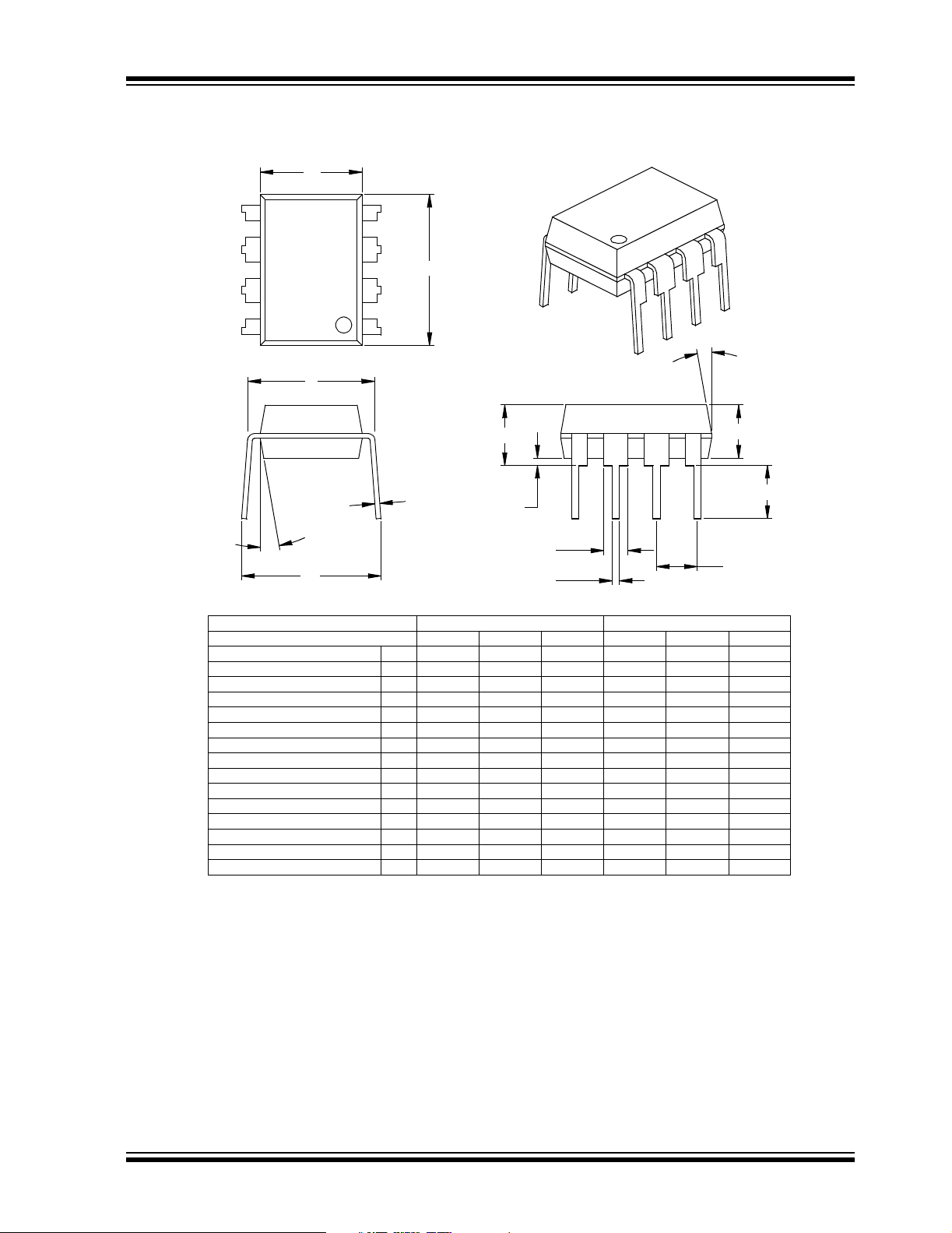
8-Lead Plastic Dual In-line (P) – 300 mil (PDIP)
E1
D
2
MCP616/7/8/9
n
E
β
eB
Number of Pins
Pitch
Top to Seating Plane A .140 .155 .170 3.56 3.94 4.32
Molded Package Thickness A2 .1 1 5 .130 .145 2.92 3.30 3.68
Base to Seating Plane A1 .015 0.38
Shoulder to Shoulder Width E .300 .313 .325 7.62 7.94 8.26
Molded Package Width E1 .240 .250 .260 6.10 6.35 6.60
Overall Length D .360 .373 .385 9.14 9.46 9.78
Tip to Seating Plane L .125 .130 .135 3.18 3.30 3.43
Lead Thickness
Upper Lead Width B1 .045 .058 .070 1.14 1.46 1.78
Lower Lead Width B .014 .018 .022 0.36 0.46 0.56
Overall Row Spacing § eB .310 .370 .430 7.87 9.40 10.92
Mold Draft Angle Top
Mold Draft Angle Bottom
* Controlling Parameter
§ Significant Characteristic
Notes:
Dimensions D and E1 do not include mold flash or protrusions. Mold flash or protrusions shall not exceed
.010” (0.254mm) per side.
JEDEC Equivalent: MS-001
Drawing No. C04-018
Dimension Limits MIN NOM MAX MIN NOM MAX
1
α
A
c
Units INCHES* MILLIMETERS
n
p
c
a
b
.008 .012 .015 0.20 0.29 0.38
A1
B1
B
88
.100 2.54
51015 51015
51015 51015
A2
L
p
© 2005 Microchip Technology Inc. DS21613B-page 19
MCP616/7/8/9
8-Lead Plastic Small Outline (SN) – Narrow, 150 mil (SOIC)
E
E1
p
D
2
B
Number of Pins
Pitch
Standoff §
Foot Angle
Lead Thickness
Mold Draft Angle Top
Mold Draft Angle Bottom
* Controlling Parameter
§ Significant Characteristic
Notes:
Dimensions D and E1 do not include mold flash or protrusions. Mold flash or protrusions shall not exceed
.010” (0.254mm) per side.
JEDEC Equivalent: MS-012
Drawing No. C04-057
n
45°
c
β
n
p
A1
φ
c
α
β
1
h
A
φ
L
048048
A1
MILLIMETERSINCHES*Units
1.27.050
α
A2
MAXNOMMINMAXNOMMINDimension Limits
88
1.751.551.35.069.061.053AOverall Height
1.551.421.32.061.056.052A2Molded Package Thickness
0.250.180.10.010.007.004
6.206.025.79.244.237.228EOverall Width
3.993.913.71.157.154.146E1Molded Package Width
5.004.904.80.197.193.189DOverall Length
0.510.380.25.020.015.010hChamfer Distance
0.760.620.48.030.025.019LFoot Length
0.250.230.20.010.009.008
0.510.420.33.020.017.013BLead Width
1512015120
1512015120
DS21613B-page 20 © 2005 Microchip Technology Inc.
8-Lead Plastic Micro Small Outline Package (MS) (MSOP)
E
E1
p
D
2
B
n 1
MCP616/7/8/9
α
A
c
(F)
β
Units
Dimension Limits
Number of Pins
Pitch
Overall Height
Molded Package Thickness
Standoff
Overall Width
Molded Package Width
Overall Length
Foot Length
Foot Angle
Lead Thickness
Lead Width
Mold Draft Angle Top
Mold Draft Angle Bottom
*Controlling Parameter
Notes:
Dimensions D and E1 do not include mold flash or protrusions. Mold flash or protrusions shall not
exceed .010" (0.254mm) per side.
JEDEC Equivalent: MO-187
Drawing No. C04-111
A2
E1
n
p
A1
E
D
L
B
α
MIN
.026 BSC
A
.030
.000
.193 TYP.
.118 BSC
.118 BSC
.016 .024
φ
c
β
.037 REFFFootprint (Reference)
0° - 8°
.003
.009
5°
5° -
L
INCHES
NOM
.033
.006
.012
φ
A1
MAX NOM
8
--
-
-
.043
.037
.006
.031
.009
.016
15°
15°
MIN
0.75
0.00
0.40
0.08
0.22
MILLIMETERS*
MAX
8
0.65 BSC
--
0.85
-
4.90 BSC
3.00 BSC
3.00 BSC
0.60
0.95 REF
0°
-
-
-
A2
1.10
0.95
0.15
0.80
8°
0.23
0.40
15°5° 15°5° -
© 2005 Microchip Technology Inc. DS21613B-page 21
MCP616/7/8/9
14-Lead Plastic Dual In-line (P) – 300 mil (PDIP)
E1
D
2
n
E
β
eB
Number of Pins
Pitch
Top to Seating Plane A .140 .155 .170 3.56 3.94 4.32
Molded Package Thickness A2 .115 .130 .145 2.92 3.30 3.68
Base to Seating Plane A1 .015 0.38
Shoulder to Shoulder Width E .300 .313 .325 7.62 7.94 8.26
Molded Package Width E1 .240 .250 .260 6.10 6.35 6.60
Overall Length D .740 .75 0 .760 18.80 19.05 19.30
Tip to Seating Plane L .125 .130 .135 3.18 3.30 3.43
Lead Thickness
Upper Lead Width B1 .045 .058 .070 1.14 1.46 1.78
Lower Lead Width B .014 .018 .022 0.36 0.46 0.56
Overall Row Spacing §
Mold Draft Angle Top
Mold Draft Angle Bottom
* Controlling Parameter
§ Significant Characteristic
Notes:
Dimensions D and E1 do not include mold flash or protrusions. Mold flash or protrusions shall not exceed
.010” (0.254mm) per side.
JEDEC Equivalent: MS-001
Drawing No. C04-005
1
A
c
A1
Dimension Limits MIN NOM MAX MIN NOM MAX
Units INCHES* MILLIMETERS
n
p
c
eB
α
β
.008 .012 .015 0.20 0.29 0.38
.310 .370 .430 7.87 9.40 10.92
5 10 15 5 10 15
5 10 15 5 10 15
B1
B
14 14
.100 2.54
α
A2
L
p
DS21613B-page 22 © 2005 Microchip Technology Inc.

14-Lead Plastic Small Outline (SL) – Narrow, 150 mil (SOIC)
E
E1
p
D
2
B
n
1
MCP616/7/8/9
45×
c
β
Number of Pins
Pitch
Foot Angle
Lead Thickne ss
Mold Draft Angle Top
Mold Draft Angle Bottom
* Controlling Parameter
§ Significant Characteristic
Notes:
Dimensions D and E1 do not include mold flash or protrusions. Mold flash or protrusions shall not exceed
.010” (0.254mm) per side.
JEDEC Equivalent: MS-012
Drawing No. C04-065
h
A
φ
L
n
p
φ
c
α
β
A1
048048
α
MILLIMETERSINCHES*Units
1.27.050
A2
MAXNOMMINMAXNOMMINDimension Limits
1414
1.751.551.35.069.061.053AOverall Height
1.551.421.32.061.056.052A2Molded Package Thickness
0.250.180.10.010.007.004A1Standoff §
6.205.995.79.244.236.228EOverall Width
3.993.903.81.157.154.150E1Molded Package Width
8.818.698.56.347.342.337DOverall Length
0.510.380.25.020.015.010hChamfer Distance
1.270.840.41.050.033.016LFoot Length
0.250.230.20.010.009.008
0.510.420.36.020.017.014BLead Width
1512015120
1512015120
© 2005 Microchip Technology Inc. DS21613B-page 23

MCP616/7/8/9
14-Lead Plastic Thin Shrink Small Outline (ST) – 4.4 mm (TSSOP)
E
E1
p
D
2
n
B
1
A
c
φ
β
Number of Pins
Pitch
Foot Angle
Lead Thickne ss
Mold Draft Angle Top
Mold Draft Angle Bottom
* Controlling Parameter
§ Significant Characteristic
Notes:
Dimensions D and E1 do not include mold flash or protrusions. Mold flash or protrusions shall not exceed
.005” (0.127mm) per side.
JEDEC Equivalent: MO-153
Drawing No. C04-087
n
p
φ
c
α
β
L
MILLIMETERS*INCHESUnits
0.65.026
α
A2A1
MAXNOMMINMAXNOMMINDimension Limits
1414
1.10.043AOverall Height
0.950.900.85.037.035.033A2Mold ed Pa ckag e Thick ness
0.150.100.05.006.004.002A1Standoff §
6.506.386.25.256.251.246EOverall Width
4.504.404.30.177.173.169E1Mold ed Pa ckag e Width
5.105.004.90.201.197.193DMolded Package Length
0.700.600.50.028.024.020LFoot Length
840840
0.200.150.09.008.006.004
0.300.250.19.012.010.007B1Lead Width
10501050
10501050
DS21613B-page 24 © 2005 Microchip Technology Inc.

APPENDIX A: REVISION HISTORY
Revision B (April 2005)
The following is the list of modifications:
1. Clarified specifications found in Section 1.0
“Electrical Character istics”.
2. Updated Section 2.0 “Typical Performance
Curves” and added input noise current density
plot.
3. Added Section 3.0 “Pin Descriptions”.
4. Updated Section 4.0 “Applications Informa-
tion”.
5. Updated the SPICE macro model and added
information on the FilterLab software, in
Section 5.0 “Design Tools”.
6. Corrected package marking information
(Section 6.0 “Packaging Information”).
7. Added Appendix A: “Revision History”.
Revision A (April 2001)
MCP616/7/8/9
• Original Release of this Document.
© 2005 Microchip Technology Inc. DS21613B-page 25

MCP616/7/8/9
NOTES:
DS21613B-page 26 © 2005 Microchip Technology Inc.

MCP616/7/8/9
PRODUCT IDENTIFICATION SYSTEM
To order or obtain information, e.g., on pricing or delivery , refer to the factory or the listed sales office.
PART NO. –X /XX
Device
PackageTemperature
Range
Device: MCP616: Single Operational Amplifier
Temperature Range: I = -40°C to +85°C
Package: MS = Plastic MSOP, 8-lead
MCP616T: Single Operational Amplifier
MCP617: Dual Operational Amplifier
MCP617T: Dual Operational Amplifier
MCP618: Single Operational Amplifier w/Chip
MCP618T: Single Operational Amplifier w/Chip
MCP619: Quad Operational Amplifier
MCP619T: Quad Operational Amplifier
P = Plastic DIP (300 mil Body), 8-lead, 14-lead
SN = Plastic SOIC (150 mil Body), 8-lead
SL = Plastic SOIC (150 mil Body), 14-lead (MCP619)
ST = Plastic TSSOP (4.4mm Body), 14-lead (MCP619)
(Tape and Reel for SOIC, MSOP)
(Tape and Reel for SOIC and MSOP)
(CS)
(CS) (Tape and Reel for SOIC and MSOP)
(Tape and Reel for SOIC and TSSOP)
Select
Select
Examples:
a) MCP616-I/P: Industrial Temperature,
b) MCP616-I/SN: Industrial Temperature,
8LD SOIC.
c) MCP616T-I/SN: Tape and Reel,
8LD SOIC.
a) MCP617-I/MS: Industrial Temperature,
b) MCP617T-I/MS: Tape and Reel,
c) MCP617-I/P: Industrial Temperature,
a) MCP618-I/SN: Industrial Temperature,
b) MCP618T-I/SN: Tape and Reel,
c) MCP618-I/P: Industrial Temperature,
a) MCP619T-I/SL: Tape and Reel,
b) MCP619T-I/ST: Tape and Reel,
c) MCP619-I/P: Industrial Temperature,
8LD PDIP.
Industrial Temperature,
8LD MSOP.
Industrial Temperature,
8LD MSOP.
8LD PDIP.
8LD SOIC.
Industrial Temperature,
8LD SOIC.
8LD PDIP.
Industrial Temperature,
14LD SOIC.
Industrial Temperature,
14LD TSSOP.
14LD PDIP.
© 2005 Microchip Technology Inc. DS21613B-page 27

MCP616/7/8/9
NOTES:
DS21613B-page 28 © 2005 Microchip Technology Inc.

Note the following details of the code protection feature on Microchip devices:
• Microchip products meet the specification contained in their particular Microchip Data Sheet.
• Microchip believes that its family of products is one of the most secure families of its kind on the market today, when used in the
intended manner and under normal conditions.
• There are dishonest and possibly illegal methods used to breach the code protection feature. All of these methods, to our
knowledge, require using the Microchip products in a manner outside the operating specifications contained in Microchip’s Data
Sheets. Most likely, the person doing so is engaged in theft of intellectual property.
• Microchip is willing to work with the customer who is concerned about the integrity of their code.
• Neither Microchip nor any other semiconductor manufacturer can guarantee the security of their code. Code protection does not
mean that we are guaranteeing the product as “unbreakable.”
Code protection is constantly evolving. We at Microchip are com mitted to continuously improving the code protect ion f eatures of our
products. Attempts to break Microchip’s code protection feature may be a violation of the Digit al Mill ennium Copyright Act. If such acts
allow unauthorized access to your software or other copyrighted work, you may have a right to sue for relief under that Act.
Information contained in this publication regarding device
applications and the like is provided only for your convenience
and may be superseded by updates. It is your responsibility to
ensure that your application meets with your specifications.
MICROCHIP MAKES NO REPRESENTATIONS OR WARRANTIES OF ANY KIND WHETHER EXPRESS OR IMPLIED,
WRITTEN OR ORAL, STATUTORY OR OTHERWISE,
RELATED TO THE INFORMATION, INCLUDING BUT NOT
LIMITED TO ITS CONDITION, QUALITY, PERFORMANCE,
MERCHANTABILITY OR FITNESS FOR PURPOSE.
Microchip disclaims all liability arising from this information and
its use. Use of M icrochip’s prod ucts as critical components in
life support systems is not authorized except with express
written approval by Microchip. No licenses are conveyed,
implicitly or otherwise, under any Microchip intellectual property
rights.
Trademarks
The Microchip name and logo, the Microchip logo, Accuron,
dsPIC, K
EELOQ, microID, MPLAB, PIC, PICmicro,
PICSTART, PRO MATE, PowerSmart, rfPIC, and
SmartShunt are registered trademarks of Microchip
Technology Incor porated in the U.S.A. and other countries.
AmpLab, FilterLab, Migratable Memory, MXDEV, MXLAB,
PICMASTER, SEEVAL, SmartSensor and The Embedded
Control Solutions Company are registered trademarks of
Microchip Technology I ncorporat ed in the U.S.A.
Analog-for-the-Digital Age, Application Maestro, dsPICDEM,
dsPICDEM.net, dsPICworks, ECAN, ECONOMONITOR,
FanSense, FlexROM, fuzzyLAB, In-Circuit Serial
Programming, ICSP, ICEPIC, Linear Active Thermistor,
MPASM, MPLIB, MPLINK, MPSIM, PICkit, PICDEM,
PICDEM.net, PICLAB, PICtail, PowerCal, PowerInfo,
PowerMate, PowerTool, rfLAB, rfPICDEM, Select Mode,
Smart Serial, SmartTel, Total Endurance and WiperLock are
trademarks of Microchip Technology Incorporated in the
U.S.A. and other countries.
SQTP is a service mark of Microchip T echnology Incorporated
in the U.S.A.
All other trademarks mentioned herein are property of their
respective companies.
© 2005, Microchip Technology Incorporated, Pr inted in the
U.S.A., All Rights Reserved.
Printed on recycled paper.
Microchip received ISO/TS-16949:2002 quality system certification for
its worldwide headquarters, design and wafer fabrication facilities in
Chandler and Tempe, Arizona and Mountain View, California in
October 2003. The Company’s quality system processes and
procedures are for its PICmicro
devices, Serial EEPROMs, microperipherals, nonvolatile memory and
analog products. In addition, Microchip’s quality system for the design
and manufacture of development systems is ISO 9001:2000 certified.
®
8-bit MCUs, KEELOQ
®
code hopping
© 2005 Microchip Technology Inc. DS21613B-page 29

WORLDWIDE SALES AND SERVICE
AMERICAS
Corporate Office
2355 West Chandler Blvd.
Chandler, AZ 85224-6199
Tel: 480-792-7200
Fax: 480-792-7277
Techn ical Su pport:
http://support.microchip.com
Web Address:
www.microchip.com
Atlanta
Alpharetta, GA
Tel: 770-640-0034
Fax: 770-640-0307
Boston
Westborough, MA
Tel: 774-760-0087
Fax: 774-760-0088
Chicago
Itasca, IL
Tel: 630-285-0071
Fax: 630-285-0075
Dallas
Addison, TX
Tel: 972-818-7423
Fax: 972-818-2924
Detroit
Farmington Hills, MI
Tel: 248-538-2250
Fax: 248-538-2260
Kokomo
Kokomo, IN
Tel: 765-864-8360
Fax: 765-864-8387
Los Angeles
Mission Viejo, CA
Tel: 949-462-9523
Fax: 949-462-9608
San Jose
Mountain View, CA
Tel: 650-215-1444
Fax: 650-961-0286
Toronto
Mississauga, Ontario,
Canada
Tel: 905-673-0699
Fax: 905-673-6509
ASIA/PACIFIC
Australia - Sydney
Tel: 61-2-9868-67 33
Fax: 61-2-9868-6755
China - Beijing
Tel: 86-10-8528-2 100
Fax: 86-10-8528-2104
China - Chengdu
Tel: 86-28-8676-6 200
Fax: 86-28-8676-6599
China - Fuzhou
Tel: 86-591-8750- 3506
Fax: 86-591-8750-3521
China - Hong Kong SAR
Tel: 852-2401-1200
Fax: 852-2401-3431
China - Shanghai
Tel: 86-21-5407-5 533
Fax: 86-21-5407-5066
China - Shenyang
Tel: 86-24-2334-2 829
Fax: 86-24-2334-2393
China - Shenzhen
Tel: 86-755-8203- 2660
Fax: 86-755-8203-1760
China - Shunde
Tel: 86-757-2839-5507
Fax: 86-757-2839-5571
China - Qingdao
Tel: 86-532-502-7 355
Fax: 86-532-502-7205
ASIA/PACIFIC
India - Bangalore
Tel: 91-80-2229-0061
Fax: 91-80-2229-0062
India - New Delhi
Tel: 91-11-5160-8631
Fax: 91-11-5160-8632
Japan - Kanagawa
Tel: 81-45-471- 6166
Fax: 81-45-471-6122
Korea - Seoul
Tel: 82-2-554-7200
Fax: 82-2-558-5932 or
82-2-558-5934
Malaysia - Penang
Tel:011-604-646-8870
Fax:011-604-646-5086
Philippines - Manila
Tel: 011-632-634-9065
Fax: 011-632-634-9069
Singapore
Tel: 65-6334-8870
Fax: 65-6334-8850
Taiwan - Kaohsiung
Tel: 886-7-536-4818
Fax: 886-7-536-4803
Taiwan - Taipei
Tel: 886-2-2500-6610
Fax: 886-2-2508-0102
Taiwan - Hsinchu
Tel: 886-3-572-9526
Fax: 886-3-572-6459
EUROPE
Austria - Weis
Tel: 43-7242-2244-399
Fax: 43-7242-2244-393
Denmark - Ballerup
Tel: 45-4450-2828
Fax: 45-4485-2829
France - Massy
Tel: 33-1-69-53 -63-20
Fax: 33-1-69-30-90-79
Germany - Ismaning
Tel: 49-89-627- 144-0
Fax: 49-89-627-144-44
Italy - Milan
Tel: 39-0331-742611
Fax: 39-0331-466781
Netherlands - Drunen
Tel: 31-416-690399
Fax: 31-416-690340
England - Berkshire
Tel: 44-118-921-5869
Fax: 44-118-921-5820
04/20/05
DS21613B-page 30 © 2005 Microchip Technology Inc.
 Loading...