

Page 1
MCP6021/1R/2/3/4
Rail-to-Rail Input/Output, 10 MHz Op Amps
Features
• Rail-to-Rail Input/Output
• Wide Bandwidth: 10 MHz (typ.)
• Low Noise: 8.7 nV/√Hz, at 10 kHz (typ.)
• Low Offset Voltage:
- Industrial Temperature: ±500 μV (max.)
- Extended Temperature: ±250 μV (max.)
• Mid-Supply V
: MCP6021 and MCP6023
REF
• Low Supply Current: 1 mA (typ.)
• Total Harmonic Distortion: 0.00053% (typ., G = 1)
• Unity Gain Stable
• Power Supply Range: 2.5V to 5.5V
• Temperature Range:
- Industrial: -40°C to +85°C
- Extended: -40°C to +125°C
Typical Applications
• Automotive
• Driving A/D Converters
• Multi-Pole Active Filters
• Barcode Scanners
• Audio Processing
• Communications
• DAC Buffer
• Test Equipment
• Medical Instrumentation
Available Tools
• SPICE Macro Model (at www.microchip.com)
•FilterLab
®
software (at www.microchip.com)
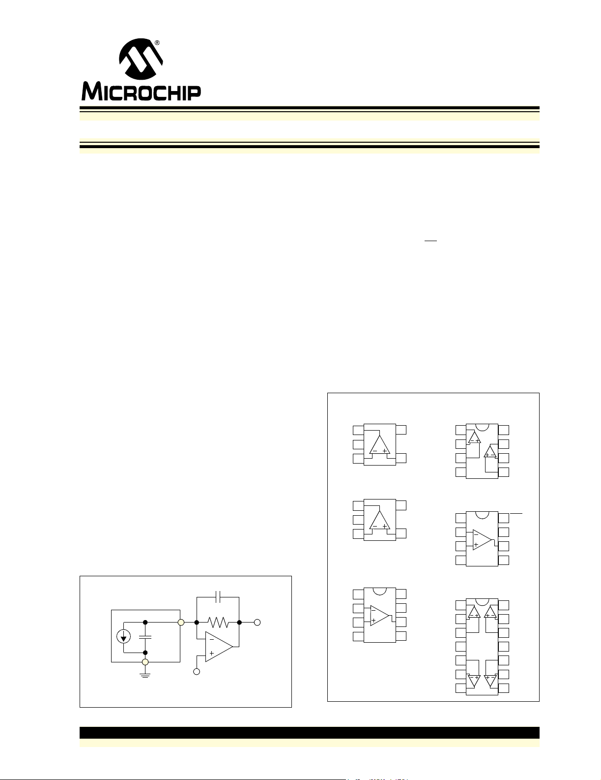
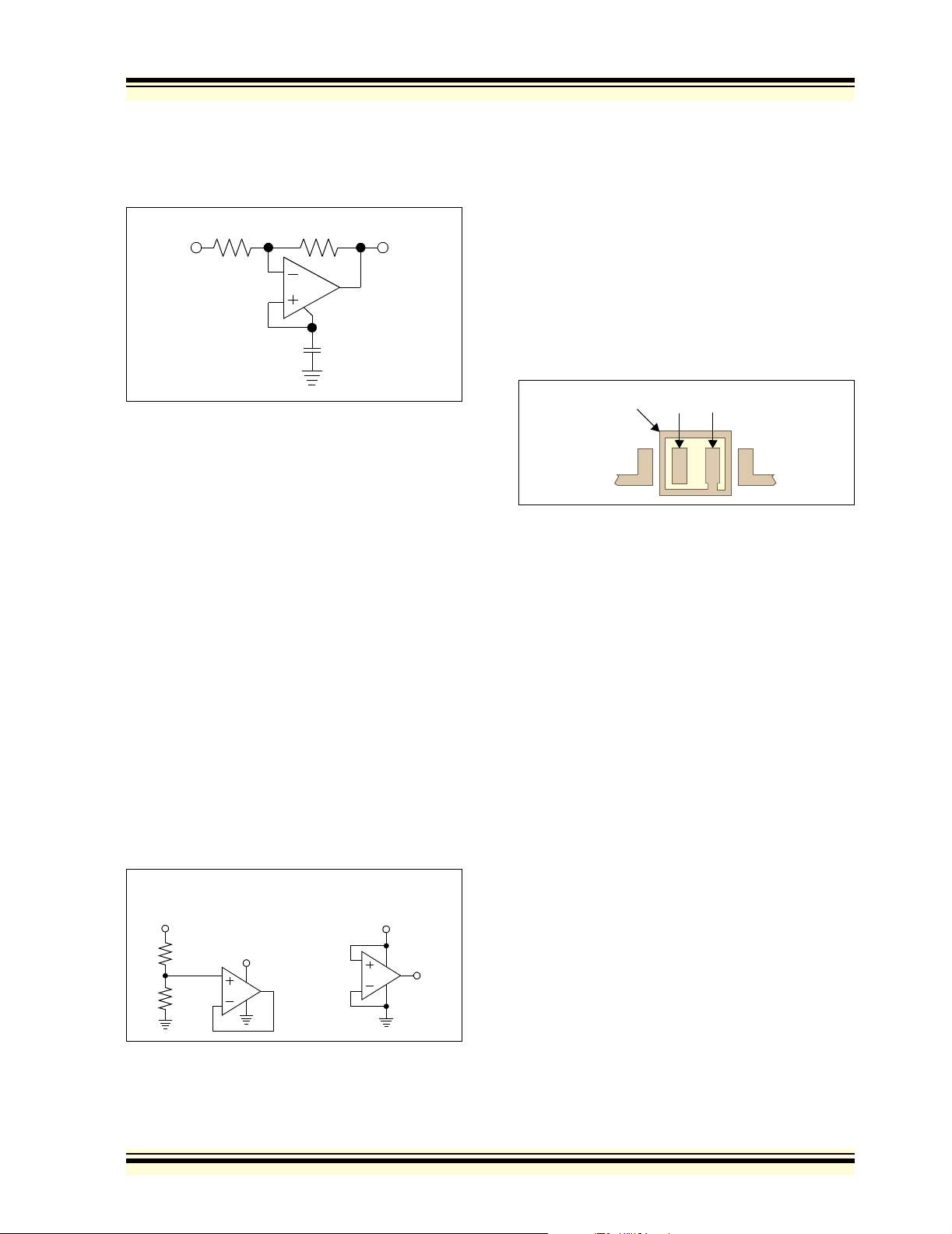
Typical Application
Photo
Detector
100 pF
Transimpedance Amplifier
5.6 pF
100 kΩ
MCP6021
VDD/2
Description
The MCP6021, MCP6021R, MCP6022, MCP6023 and
MCP6024 from Microchip Technology Inc. are rail-torail input and output op amps with high performance.
Key specifications include: wide bandwidth (10 MHz),
low noise (8.7 nV/√Hz), low input offset voltage and low
distortion (0.00053% THD+N). The MCP6023 also
offers a Chip Select pin (CS
) that gives power savings
when the part is not in use.
The single MCP6021 and MCP6021R are available in
SOT-23-5. The single MCP6021, single MCP6023 and
dual MCP6022 are available in 8-lead PDIP, SOIC and
TSSOP. The Extended Temperature single MCP6021
is available in 8-lead MSOP. The quad MCP6024 is
offered in 14-lead PDIP, SOIC and TSSOP packages.
The MCP6021/1R/2/3/4 family is available in Industrial
and Extended temperature ranges. It has a power
supply range of 2.5V to 5.5V.
Package Types
MCP6021
SOT-23-5
V
1
OUT
V
2
SS
VIN+
3
MCP6021R
SOT-23-5
V
1
OUT
V
2
DD
VIN+
3
MCP6021
PDIP SOIC,
MSOP, TSSOP
NC
1
–
V
2
IN
VIN+
3
V
4
SS
5
4
5
4
8
7
6
5
V
DD
VIN–
V
SS
VIN–
NC
V
DD
V
OUT
V
REF
V
V
V
V
V
V
V
V
V
MCP6022
PDIP SOIC, TSSOP
1
OUTA
–
2
INA
+
3
INA
V
4
SS
MCP6023
PDIP SOIC, TSSOP
NC
1
VIN–
2
+
V
3
IN
V
4
SS
MCP6024
PDIP SOIC, TSSOP
1
OUTA
–
2
INA
+
3
INA
V
4
DD
+
5
INB
–
6
INB
7
OUTB
14
13
12
11
10
V
8
DD
V
7
OUTB
V
–
6
INB
+
V
5
INB
CS
8
V
7
DD
V
6
OUT
V
5
REF
V
OUTD
V
–
IND
+
V
IND
V
SS
V
+
INC
–
V
9
INC
V
8
OUTC
© 2006 Microchip Technology Inc. DS21685C-page 1
Page 2
MCP6021/1R/2/3/4
1.0 ELECTRICAL CHARACTERISTICS
† Notice: Stresses above those listed under “Absolute
Maximum Ratings” may cause permanent damage to the
device. This is a stress rating only and functional operation of
the device at those or any other conditions above those
Absolute Maximum Ratings †
indicated in the operational listings of this specification is not
implied. Exposure to maximum rating conditions for extended
VDD–VSS........................................................................7.0V
All Inputs and Outputs.................... V
Difference Input Voltage ...................................... |V
– 0.3V to VDD+0.3V
SS
DD–VSS
|
periods may affect device reliability.
Output Short Circuit Current ..................................continuous
Current at Input Pins ....................................................±2 mA
Current at Output and Supply Pins ............................±30 mA
Storage Temperature.....................................-65°C to +150°C
Junction Temperature..................................................+150°C
ESD Protection on all pins (HBM; MM)................ ≥ 2 kV; 200V
DC ELECTRICAL CHARACTERISTICS
Electrical Specifications: Unless otherwise indicated, TA = +25°C, VDD = +2.5V to +5.5V, VSS = GND, VCM = VDD/2, V
=10kΩ to VDD/2.
and R
L
Parameters Sym Min Typ Max Units Conditions
Input Offset
Input Offset Voltage:
Industrial Temperature Parts V
Extended Temperature Parts V
Extended Temperature Parts V
Input Offset Voltage Temperature Drift ΔV
OS
OS
OS
OS
/ΔT
Power Supply Rejection Ratio PSRR 74 90 — dB V
Input Current and Impedance
Input Bias Current I
Industrial Temperature Parts I
Extended Temperature Parts I
Input Offset Current I
Common-Mode Input Impedance Z
Differential Input Impedance Z
B
B
B
OS
CM
DIFF
Common-Mode
Common-Mode Input Range V
CMR
Common-Mode Rejection Ratio CMRR 74 90 — dB V
CMRR 70 85 — dB V
CMRR 74 90 — dB V
Voltage Reference (MCP6021 and MCP6023 only)
Accuracy (V
V
REF
V
Temperature Drift ΔV
REF
REF–VDD
/2) V
REF_ACC
/ΔT
REF
Open-Loop Gain
DC Open-Loop Gain (Large Signal) A
OL
Output
Maximum Output Voltage Swing V
Output Short Circuit Current I
OL
, V
SC
I
SC
Power Supply
Supply Voltage V
Quiescent Current per Amplifier I
S
Q
-500 — +500 μVVCM = 0V
-250 — +250 μVVCM = 0V, VDD = 5.0V
-2.5 — +2.5 mV VCM = 0V, VDD = 5.0V
= -40°C to +125°C
T
A
—±3.5—μV/°C TA = -40°C to +125°C
A
CM
—1—pA
— 30 150 pA TA = +85°C
— 640 5,000 pA TA = +125°C
—±1—pA
—1013||6 — Ω||pF
—1013||3 — Ω||pF
VSS-0.3 — VDD+0.3 V
DD
DD
DD
-50 — +50 mV
— ±100 — μV/°C TA = -40°C to +125°C
A
90 110 — dB VCM = 0V,
V
OUT
OHVSS
+15 — VDD-20 mV 0.5V output overdrive
—±30—mAVDD = 2.5V
—±22—mAVDD = 5.5V
2.5 — 5.5 V
0.5 1.0 1.35 mA IO = 0
= 0V
= 5V, VCM = -0.3V to 5.3V
= 5V, VCM = 3.0V to 5.3V
= 5V, VCM = -0.3V to 3.0V
= VSS+0.3V to VDD-0.3V
OUT
≈ VDD/2
DS21685C-page 2 © 2006 Microchip Technology Inc.
Page 3
MCP6021/1R/2/3/4
AC ELECTRICAL CHARACTERISTICS
Electrical Specifications: Unless otherwise indicated, TA = +25°C, VDD = +2.5V to +5.5V, VSS = GND, VCM = VDD/2,
≈ VDD/2, RL =10kΩ to VDD/2 and CL = 60 pF.
V
OUT
Parameters Sym Min Typ Max Units Conditions
AC Response
Gain Bandwidth Product GBWP — 10 — MHz
Phase Margin at Unity-Gain PM — 65 — ° G = +1
Settling Time, 0.2% t
SETTLE
Slew Rate SR — 7.0 — V/μs
Total Harmonic Distortion Plus Noise
f = 1 kHz, G = +1 V/V THD+N — 0.00053 — % V
f = 1 kHz, G = +1 V/V, R
= 600Ω THD+N — 0.00064 — % V
L
f = 1 kHz, G = +1 V/V THD+N — 0.0014 — % V
f = 1 kHz, G = +10 V/V THD+N — 0.0009 — % V
f = 1 kHz, G = +100 V/V THD+N — 0.005 — % V
Noise
Input Noise Voltage E
Input Noise Voltage Density e
Input Noise Current Density i
ni
ni
ni
— 250 — ns G = +1, V
OUT
= 5.0V, BW = 22 kHz
V
DD
OUT
= 5.0V, BW = 22 kHz
V
DD
OUT
OUT
OUT
= 100 mV
OUT
= 0.25V to 3.25V (1.75V ± 1.50VPK),
= 0.25V to 3.25V (1.75V ± 1.50VPK),
= 4V
, VDD = 5.0V, BW = 22 kHz
P-P
= 4V
, VDD = 5.0V, BW = 22 kHz
P-P
= 4V
, VDD = 5.0V, BW = 22 kHz
P-P
—2.9—μVp-p f = 0.1 Hz to 10 Hz
—8.7—nV/√Hz f = 10 kHz
—3—fA/√Hz f = 1 kHz
p-p
MCP6023 CHIP SELECT (CS
) ELECTRICAL CHARACTERISTICS
Electrical Specifications: Unless otherwise indicated, T
≈ VDD/2, RL =10kΩ to VDD/2 and CL = 60 pF.
V
OUT
Parameters Sym Min Typ Max Units Conditions
CS
Low Specifications
CS
Logic Threshold, Low V
CS
Input Current, Low I
IL
CSL
CS High Specifications
CS
Logic Threshold, High V
CS
Input Current, High I
GND Current I
Amplifier Output Leakage I
IH
CSH
SS
O(LEAK)
CS Dynamic Specifications
CS
Low to Amplifier Output Turn-on Time t
CS
High to Amplifier Output High-Z Time t
Hysteresis V
ON
OFF
HYST
= +25°C, VDD = +2.5V to +5.5V, VSS = GND, VCM = VDD/2,
A
V
-1.0 0.01 — μACS = V
0.8 V
—0.012.0 μACS = V
-2 -0.05 — μACS = V
—0.01— μACS = V
—0.2VDDV
SS
—VDDV
DD
SS
DD
DD
DD
—210μs G = +1, VIN = VSS,
= 0.2VDD to V
CS
OUT
—0.01— μs G = +1, VIN = VSS,
CS
= 0.8VDD to V
OUT
—0.6— VVDD = 5.0V, Internal Switch
= 0.45VDD time
= 0.05VDD time
© 2006 Microchip Technology Inc. DS21685C-page 3
Page 4
MCP6021/1R/2/3/4
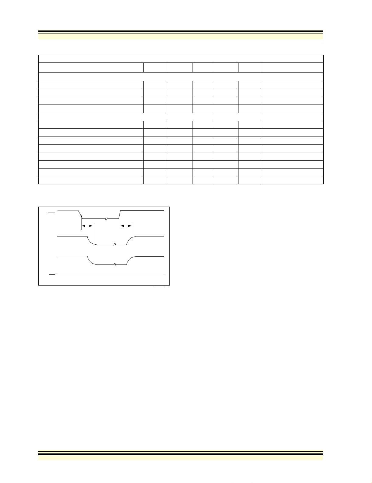
TEMPERATURE CHARACTERISTICS
Electrical Specifications: Unless otherwise indicated, VDD = +2.5V to +5.5V and VSS = GND.
Parameters Sym Min Typ Max Units Conditions
Temperature Ranges
Industrial Temperature Range T
Extended Temperature Range T
Operating Temperature Range T
Storage Temperature Range T
Thermal Package Resistances
Thermal Resistance, 5L-SOT-23 θ
Thermal Resistance, 8L-PDIP θ
Thermal Resistance, 8L-SOIC θ
Thermal Resistance, 8L-MSOP θ
Thermal Resistance, 8L-TSSOP θ
Thermal Resistance, 14L-PDIP θ
Thermal Resistance, 14L-SOIC θ
Thermal Resistance, 14L-TSSOP θ
Note 1: The industrial temperature devices operate over this extended temperature range, but with reduced performance. In any
case, the internal junction temperature (T
A
A
A
A
JA
JA
JA
JA
JA
JA
JA
JA
) must not exceed the absolute maximum specification of 150°C.
J
-40 — +85 °C
-40 — +125 °C
-40 — +125 °C Note 1
-65 — +150 °C
—256— °C/W
—85—°C/W
—163— °C/W
—206— °C/W
—124— °C/W
—70—°C/W
—120— °C/W
—100— °C/W
CS
V
OUT
I
SS
I
CS
t
ON
High-Z
-50 nA (typ.)
10 nA (typ.)
Amplifier On
-1 mA (typ.)
10 nA (typ.) 10 nA (typ.)
t
OFF
High-Z
-50 nA (typ.)
FIGURE 1-1: Timing diagram for the CS pin on the MCP6023.
DS21685C-page 4 © 2006 Microchip Technology Inc.
Page 5
MCP6021/1R/2/3/4
2.0 TYPICAL PERFORMANCE CURVES
Note: The graphs and tables provided following this note are a statistical summary based on a limited number of
samples and are provided for informational purposes only. The performance characteristics listed herein
are not tested or guaranteed. In some graphs or tables, the data presented may be outside the specified
operating range (e.g., outside specified power supply range) and therefore outside the warranted range.
Note: Unless otherwise indicated, TA=+25°C, VDD=+2.5Vto+5.5V, VSS= GND, VCM=VDD/2, V
=10kΩ to VDD/2 and CL=60 pF.
R
L
16%
14%
12%
10%
Percentage of Occurances
8%
6%
4%
2%
0%
I-Temp
Parts
-500
-400
-300
-200
-100
Input Offset Voltage (μV)
0
1192 Samples
V
CM
T
= +25°C
A
100
200
= 0V
300
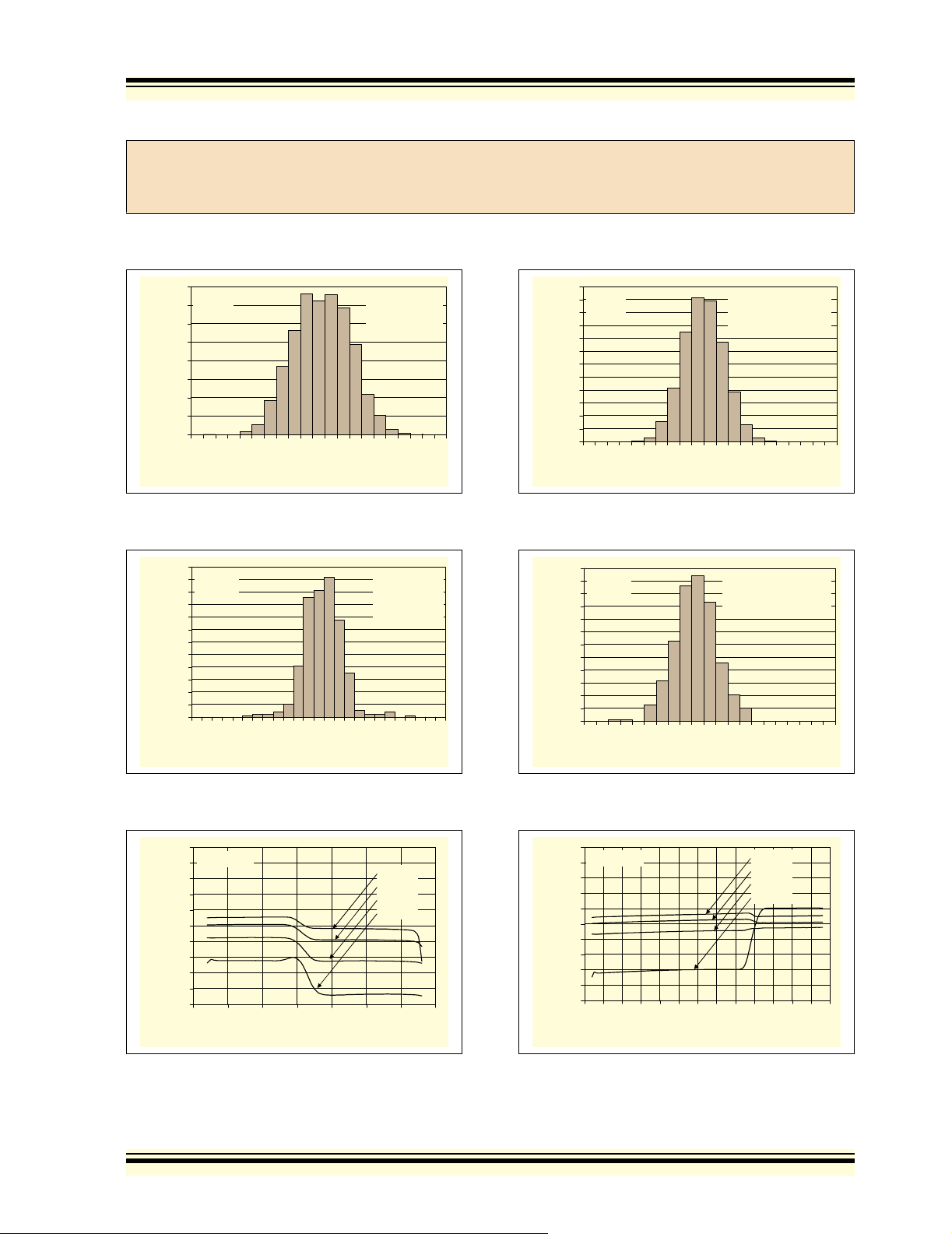
FIGURE 2-1: Input Offset Voltage, (Industrial Temperature Parts).
24%
22%
20%
18%
16%
14%
12%
10%
Percentage of Occurances
8%
6%
4%
2%
0%
E-Temp
Parts
-240
-200
0
-80
-160
-40
-120
Input Offset Voltage (μV)
40
80
438 Samples
V
= 5.0V
DD
= 0V
V
CM
T
= +25°C
A
120
160
400
200
500
240
24%
22%
20%
18%
16%
14%
12%
10%
8%
6%
4%
Percentage of Occurances
2%
0%
I-Temp
Parts
-20
-16
-8
-12
Input Offset Voltage Drift (μV/°C)
-4
1192 Samples
= 0V
V
CM
T
= -40°C to +85°C
A
0
4
8
FIGURE 2-4: Input Offset Voltage Drift, (Industrial Temperature Parts).
24%
22%
20%
18%
16%
14%
12%
10%
Percentage of Occurances
8%
6%
4%
2%
0%
E-Temp
Parts
-20
-16
-8
-12
Input Offset Voltage Drift (μV/°C)
-4
438 Samples
V
= 0V
CM
T
= -40°C to +125°C
A
0
4
8
OUT
12
12
≈ VDD/2,
16
20
16
20
FIGURE 2-2: Input Offset Voltage, (Extended Temperature Parts).
500
VDD = 2.5V
400
300
200
100
0
-100
-200
-300
Input Offset Voltage (μV)
-400
-500
-0.50.00.51.01.52.02.53.0
Common Mode Input Voltage (V)
-40°C
+25°C
+85°C
+125°C
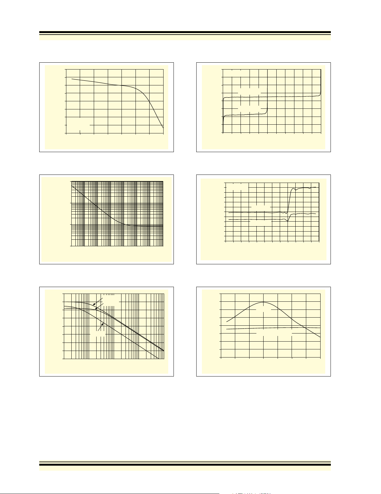
FIGURE 2-3: Input Offset Voltage vs.
Common Mode Input Voltage with V
= 2.5V.
DD
FIGURE 2-5: Input Offset Voltage Drift, (Extended Temperature Parts).
Input Offset Voltage (μV)
500
400
300
200
100
-100
-200
-300
-400
-500
VDD = 5.5V
0
-0.5
0.0
0.5
1.0
1.5
2.0
2.5
Common Mode Input Voltage (V)
3.0
3.5
-40°C
+25°C
+85°C
+125°C
4.0
4.5
5.0
5.5
FIGURE 2-6: Input Offset Voltage vs. Common Mode Input Voltage with VDD = 5.5V.
6.0
© 2006 Microchip Technology Inc. DS21685C-page 5
Page 6
MCP6021/1R/2/3/4
Note: Unless otherwise indicated, TA=+25°C, VDD=+2.5Vto+5.5V, VSS= GND, VCM=VDD/2, V
=10kΩ to VDD/2 and CL=60 pF.
R
L
100
50
0
-50
-100
-150
-200
VDD = 5.0V
-250
Input Offset Voltage (μV)
V
= 0V
CM
-300
-50 -25 0 25 50 75 100 125
Ambient Temperature (°C)
FIGURE 2-7: Input Offset Voltage vs. Temperature.
1,000
100
Hz)
(nV/
10
Input Noise Voltage Density
1.E-01 1.E+00 1.E+01 1.E+02 1.E+03 1.E+04 1.E+05 1.E+06
1
0.1 1 10 100 1k 10k 1M100k
Frequency (Hz)
200
VCM = VDD/2
150
Input Offset Voltage (μV)
100
50
0
-50
-100
-150
-200
VDD = 5.5V
VDD = 2.5V
0.0 0.5 1.0 1.5 2.0 2.5 3.0 3.5 4.0 4.5 5.0 5.5
Output Voltage (V)
FIGURE 2-10: Input Offset Voltage vs. Output Voltage.
24
VDD = 5.0V
22
20
18
16
14
Hz)
12
10
(nV/
8
6
4
2
Input Noise Voltage Density
0
-0.5
f = 1 kHz
f = 10 kHz
0.0
0.5
1.0
1.5
2.0
2.5
3.0
Common Mode Input Voltage (V)
3.5
OUT
4.0
≈ VDD/2,
4.5
5.0
5.5
FIGURE 2-8: Input Noise Voltage Density vs. Frequency.
100
90
80
70
60
50
40
CMRR, PSRR (dB)
30
1.E+02 1.E+03 1.E+04 1.E+05 1.E+06
20
100 1k 10k 100k 1M
PSRR+
PSRR-
CMRR
Frequency (Hz)
FIGURE 2-9: CMRR, PSRR vs. Frequency.
FIGURE 2-11: Input Noise Voltage Density vs. Common Mode Input Voltage.
110
105
100
95
90
85
80
PSRR, CMRR (dB)
75
70
-50 -25 0 25 50 75 100 125
CMRR
PSRR (VCM = 0V)
Ambient Temperature (°C)
FIGURE 2-12: CMRR, PSRR vs. Temperature.
DS21685C-page 6 © 2006 Microchip Technology Inc.
Page 7
MCP6021/1R/2/3/4
Note: Unless otherwise indicated, TA=+25°C, VDD=+2.5Vto+5.5V, VSS= GND, VCM=VDD/2, V
=10kΩ to VDD/2 and CL=60 pF.
R
L
10,000
Input Bias, Offset Currents (pA)
VDD = 5.5V
1,000
100
10
1
0.0 0.5 1.0 1.5 2.0 2.5 3.0 3.5 4.0 4.5 5.0 5.5
Common Mode Input Voltage (V)
IB, TA = +125°C
IOS, TA = +125°C
IB, TA = +85°C
IOS, TA = +85°C
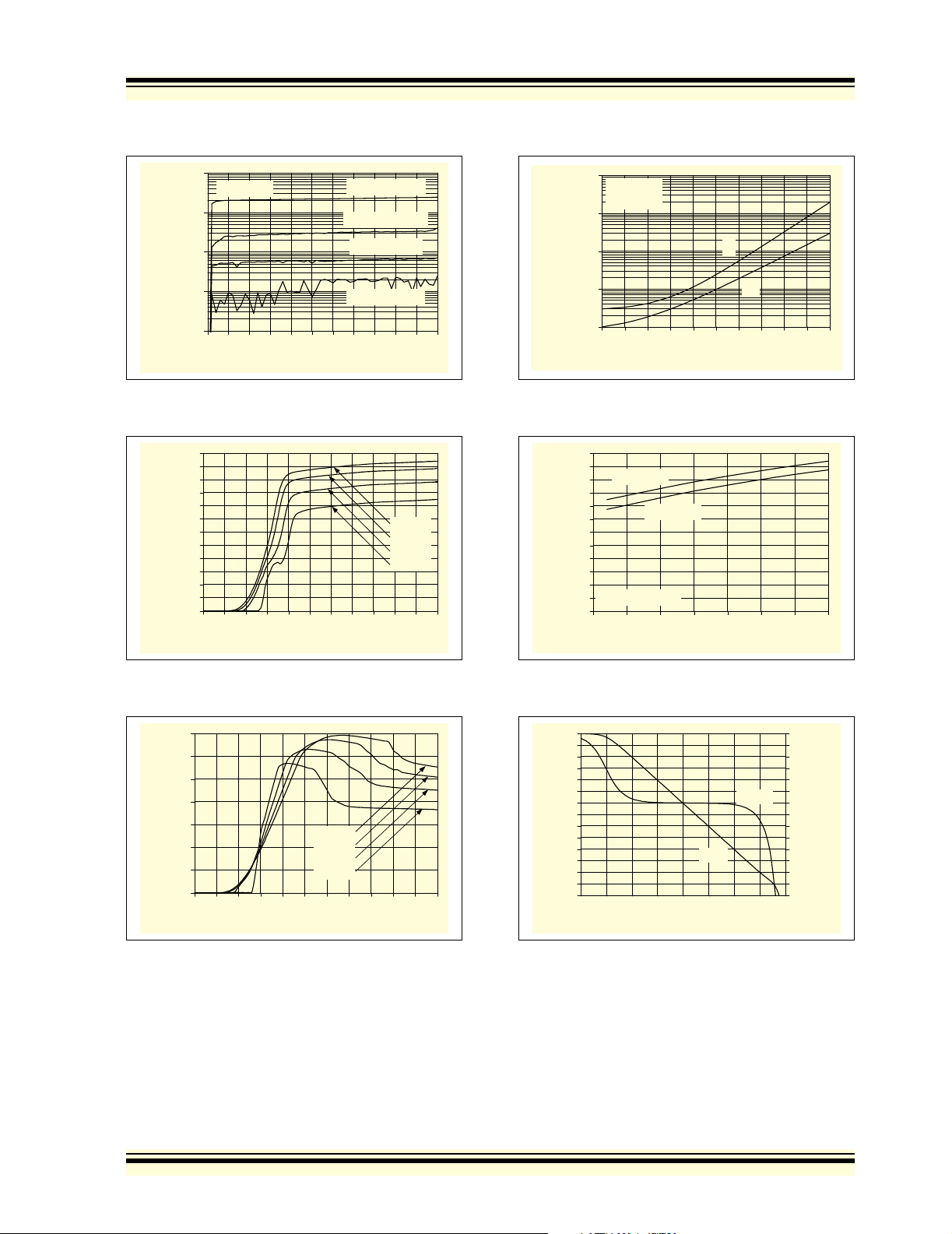
FIGURE 2-13: Input Bias, Offset Currents vs. Common Mode Input Voltage.
1.2
1.1
1.0
0.9
0.8
0.7
0.6
0.5
0.4
(mA/amplifier)
0.3
Quiescent Current
0.2
0.1
0.0
0.0 0.5 1.0 1.5 2.0 2.5 3.0 3.5 4.0 4.5 5.0 5.5
Power Supply Voltage (V)
+125°C
+85°C
+25°C
-40°C
10,000
(pA)
Input Bias, Offset Currents
VCM = V
DD
VDD = 5.5V
1,000
I
100
10
1
25 35 45 55 65 75 85 95 105 115 125
Ambient Temperature (°C)
B
I
OS
FIGURE 2-16: Input Bias, Offset Currents vs. Temperature.
1.2
1.1
VDD = 5.5V
1.0
0.9
0.8
0.7
0.6
0.5
0.4
(mA/amplifier)
0.3
Quiescent Current
0.2
VCM = VDD - 0.5V
0.1
0.0
-50 -25 0 25 50 75 100 125
VDD = 2.5V
Ambient Temperature (°C)
OUT
≈ VDD/2,
FIGURE 2-14: Quiescent Current vs. Supply Voltage.
35
30
25
20
(mA)
15
10
5
Output Short Circuit Current
0
0.00.51.01.52.02.53.03.54.04.55.05.5
+125°C
+85°C
+25°C
-40°C
Supply Voltage (V)
FIGURE 2-15: Output Short-Circuit Current vs. Supply Voltage.
FIGURE 2-17: Quiescent Current vs. Temperature.
120
110
100
90
80
70
60
50
40
30
20
10
Open-Loop Gain (dB)
0
-10
1.E+00 1.E+01 1.E+02 1.E+03 1.E+04 1.E+0 5 1.E+06 1.E+07 1.E+ 08
-20
1 10010 1k 100k10k 1M 100M10M
Frequency (Hz)
Gain
Phase
0
-15
-30
-45
-60
-75
-90
-105
-120
-135
-150
-165
-180
-195
-210
Open-Loop Phase (°)
FIGURE 2-18: Open-Loop Gain, Phase vs. Frequency.
© 2006 Microchip Technology Inc. DS21685C-page 7
Page 8
MCP6021/1R/2/3/4
Note: Unless otherwise indicated, TA=+25°C, VDD=+2.5Vto+5.5V, VSS= GND, VCM=VDD/2, V
=10kΩ to VDD/2 and CL=60 pF.
R
L
130
VDD = 5.5V
120
110
100
90
DC Open-Loop Gain (dB)
1.E+02 1.E+03 1.E+04 1.E+05
80
100 1k 10k 100k
Load Resistance (Ω)
VDD = 2.5V
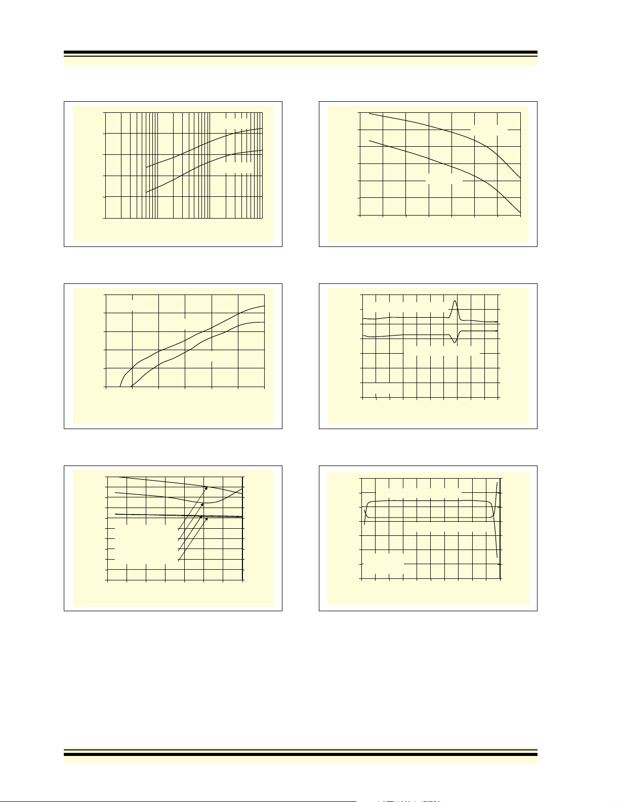
FIGURE 2-19: DC Open-Loop Gain vs. Load Resistance.
120
VCM = VDD/2
110
100
90
80
DC Open-Loop Gain (dB)
70
0.00 0.05 0.10 0.15 0.20 0.25 0.30
VDD = 5.5V
VDD = 2.5V
Output Voltage Headroom (V);
- VOH or VOL - V
V
DD
SS
120
115
110
105
100
95
DC Open-Loop Gain (dB)
90
-50 -25 0 25 50 75 100 125
VDD = 2.5V
Ambient Temperature (°C)
VDD = 5.5V
FIGURE 2-22: DC Open-Loop Gain vs. Temperature.
14
Gain Bandwidth Product
12
10
8
(MHz)
6
4
2
Gain Bandwidth Product
VDD = 5.0V
0
0.00.51.01.52.02.53.03.54.04.55.0
Phase Margin, G = +1
Common Mode Input Voltage (V)
OUT
≈ VDD/2,
105
90
75
60
45
30
15
Phase Margin, G = +1 (°)
0
FIGURE 2-20: Small Signal DC Open-Loop Gain vs. Output Voltage Headroom.
10
9
8
7
6
5
GBWP, VDD = 5.5V
(MHz)
4
GBWP, V
PM, V
3
PM, V
2
Gain Bandwidth Product
1
0
-50 -25 0 25 50 75 100 125
= 2.5V
DD
= 2.5V
DD
= 5.5V
DD
Ambient Temperature (°C)
100
90
80
70
60
50
40
30
20
10
0
Phase Margin, G = +1 (°)
FIGURE 2-21: Gain Bandwidth Product, Phase Margin vs. Temperature.
FIGURE 2-23: Gain Bandwidth Product, Phase Margin vs. Common Mode Input Voltage.
14
12
Gain Bandwidth Product
10
8
(MHz)
6
4
VDD = 5.0V
2
Gain Bandwidth Product
V
= VDD/2
CM
0
0.0 0.5 1.0 1.5 2.0 2.5 3.0 3.5 4.0 4.5 5.0
Phase Margin, G = +1
Output Voltage (V)
105
90
75
60
45
30
15
0
Phase Margin, G = +1 (°)
FIGURE 2-24: Gain Bandwidth Product, Phase Margin vs. Output Voltage.
DS21685C-page 8 © 2006 Microchip Technology Inc.
Page 9
MCP6021/1R/2/3/4
Note: Unless otherwise indicated, TA=+25°C, VDD=+2.5Vto+5.5V, VSS= GND, VCM=VDD/2, V
=10kΩ to VDD/2 and CL=60 pF.
R
L
11
Falling, VDD = 5.5V
10
Rising, V
9
8
7
6
5
4
3
Slew Rate (V/μs)
2
1
0
-50 -25 0 25 50 75 100 125
= 5.5V
DD
Falling, VDD = 2.5V
Rising, V
Ambient Temperature (°C)
= 2.5V
DD
FIGURE 2-25: Slew Rate vs. Temperature.
FIGURE 2-28: Maximum Output Voltage
10
VDD = 5.5V
)
P-P
1
Swing (V
Maximum Output Voltage
1.E+04 1.E+05 1. E+06 1.E+07
0.1
10k 100k 1M 10M
VDD = 2.5V
Frequency (Hz)
Swing vs. Frequency.
0.1000%
0.0100%
THD+N (%)
0.0010%
0.0001%
f = 1 kHz
BW
= 22 kHz
Meas
V
= 5.0V
G = +100 V/V
G = +10 V/V
G = +1 V/V
0.0 0.5 1.0 1.5 2.0 2.5 3.0 3.5 4.0 4.5 5.0
Output Voltage (V
DD
)
P-P
0.1000%
0.0100%
THD+N (%)
0.0010%
0.0001%
G = +100 V/V
G = +10 V/V
G = +1 V/V
0.0 0.5 1.0 1.5 2.0 2.5 3.0 3.5 4.0 4.5 5.0
Output Voltage (V
f = 20 kHz
BW
Meas
V
= 5.0V
DD
P-P
OUT
= 80 kHz
)
≈ VDD/2,
FIGURE 2-26: Total Harmonic Distortion
plus Noise vs. Output Voltage with f = 1 kHz.
6
5
4
3
2
1
0
Input, Output Voltage (V)
-1
0 102030405060708090100
V
OUT
V
IN
Time (10 μs/div)
VDD = 5.0V
G = +2 V/V
FIGURE 2-27: The MCP6021/1R/2/3/4 family shows no phase reversal under overdrive.
FIGURE 2-29: Total Harmonic Distortion
plus Noise vs. Output Voltage with f = 20 kHz.
135
130
125
120
(dB)
115
110
Channel to Channel Separation
G = +1 V/V
1.E+03 1.E+04 1.E+0 5 1.E+0 6
105
1k 1M100k10k
Frequency (Hz)
FIGURE 2-30: Channel-to-Channel Separation vs. Frequency (MCP6022 and MCP6024 only).
© 2006 Microchip Technology Inc. DS21685C-page 9
Page 10
MCP6021/1R/2/3/4
Note: Unless otherwise indicated, TA=+25°C, VDD=+2.5Vto+5.5V, VSS= GND, VCM=VDD/2, V
=10kΩ to VDD/2 and CL=60 pF.
R
L
1,000
(mV)
SS
100
-V
OL
or V
10
OH
-V
DD
V
Output Voltage Headroom;
VOL - V
SS
VDD - V
OH
1
0.01 0.1 1 10
Output Current Magnitude (mA)
FIGURE 2-31: Output Voltage Headroom vs. Output Current.
6.E-02
5.E-02
4.E-02
3.E-02
2.E-02
1.E-02
0.E+00
-1.E-02
-2.E-02
-3.E-02
-4.E-02
Output Voltage (10 mV/div)
-5.E-02
-6.E-02
0.E+00 2.E-07 4.E-07 6.E-07 8.E-07 1.E-06 1.E-06 1.E-06 2.E- 06 2.E-06 2.E-06
Time (200 ns/div)
G = +1 V/V
FIGURE 2-34: Output Voltage Headroom vs. Temperature.
10
VOL - V
VDD - V
SS
OH
Output Voltage Headroom
9
8
(mV)
7
SS
6
-V
OL
5
4
or V
OH
3
-V
2
DD
V
1
0
-50 -25 0 25 50 75 100 125
Ambient Temperature (°C)
6.E-02
5.E-02
4.E-02
3.E-02
2.E-02
1.E-02
0.E+00
-1.E-02
-2.E-02
-3.E-02
-4.E-02
Output Voltage (10 mV/div)
-5.E-02
-6.E-02
0.E+00 2.E-07 4.E-07 6.E-07 8 .E-07 1.E-06 1.E-06 1.E-06 2.E-06 2.E-06 2.E-06
G = -1 V/V
= 1 k
R
Ω
F
Time (200 ns/div)
OUT
≈ VDD/2,
FIGURE 2-32: Small-Signal Non-inverting Pulse Response.
5.0
4.5
4.0
3.5
3.0
2.5
2.0
1.5
Output Voltage (V)
1.0
0.5
0.E+00 5.E-07 1.E-06 2.E-06 2 .E-06 3.E-06 3.E-06 4.E-06 4.E-06 5.E-06 5.E-06
0.0
Time (500 ns/div)
G = +1 V/V
FIGURE 2-33: Large-Signal Non-inverting Pulse Response.
FIGURE 2-35: Small-Signal Inverting Pulse Response.
5.0
4.5
4.0
3.5
3.0
2.5
2.0
1.5
Output Voltage (V)
1.0
0.5
0.E+00 5.E-07 1.E-06 2.E-06 2.E -06 3.E-06 3.E-06 4.E-06 4.E-06 5.E -06 5.E-06
0.0
G = -1 V/V
= 1 kΩ
R
F
Time (500 ns/div)
FIGURE 2-36: Large-Signal Inverting Pulse Response.
DS21685C-page 10 © 2006 Microchip Technology Inc.
Page 11
MCP6021/1R/2/3/4
Note: Unless otherwise indicated, TA=+25°C, VDD=+2.5Vto+5.5V, VSS= GND, VCM=VDD/2, V
=10kΩ to VDD/2 and CL=60 pF.
R
L
50
/2
40
DD
30
– V
20
REF
10
0
(mV)
-10
-20
Accuracy; V
-30
REF
-40
V
-50
0.0 0.5 1.0 1.5 2.0 2.5 3.0 3.5 4.0 4.5 5.0 5.5
FIGURE 2-37: V
Power Supply Voltage (V)
Accuracy vs. Supply
REF
Voltage (MCP6021 and MCP6023 only).
1.6
Op Amp
1.4
turns on here
1.2
1.0
CS swept
0.8
high to low
0.6
(mA/amplifier)
VDD = 2.5V
0.4
Quiescent Current
G = +1 V/V
0.2
V
= 1.25V
IN
0.0
0.0 0.5 1.0 1.5 2.0 2.5
Chip Select Voltage (V)
Op Amp
shuts off here
Hysteresis
CS swept
low to high
FIGURE 2-40: V
Temperature (MCP6021 and MCP6023 only).
50
/2
DD
– V
REF
Accuracy; V
REF
V
Quiescent Current
Representative Part
40
30
20
10
0
(mV)
-10
-20
-30
-40
-50
-50 -25 0 25 50 75 100 125
Ambient Temperature (°C)
REF
1.6
Op Amp
1.4
turns on here
1.2
1.0
0.8
0.6
(mA/amplifier)
0.4
0.2
0.0
CS swept
high to low
VDD = 5.5V
G = +1 V/V
V
= 2.75V
IN
0.00.51.01.52.02.53.03.54.04.55.05.5
Chip Select Voltage (V)
VDD = 5.5V
VDD = 2.5V
Accuracy vs.
Op Amp
shuts off here
Hysteresis
CS swept
low to high
OUT
≈ VDD/2,
FIGURE 2-38: Chip Select (CS
(MCP6023 only) with V
5.5
5.0
4.5
4.0
3.5
3.0
2.5
2.0
1.5
Output
Output Voltage (V)
1.0
Chip Select Voltage,
on
0.5
0.0
0.0E+00 5.0E-06 1.0E-05 1.5E-05 2.0E-05 2.5E-05 3. 0E-05 3.5E-0 5
-0.5
= 2.5V.
DD
CS Voltage
V
OUT
Output High-Z
Time (5 μs/div)
FIGURE 2-39: Chip Select (CS
) Hysteresis
VDD = 5.0V
G = +1 V/V
V
= V
IN
SS
Output
on
) to
Amplifier Output Response Time (MCP6023
only).
FIGURE 2-41: Chip Select (CS
(MCP6023 only) with V
= 5.5V.
DD
) Hysteresis
© 2006 Microchip Technology Inc. DS21685C-page 11
Page 12

MCP6021/1R/2/3/4
3.0 PIN DESCRIPTIONS
Descriptions of the pins are listed in Table 3-1.
TABLE 3-1: PIN FUNCTION TABLE
MCP6021
(PDIP,
SOIC,
MSOP,
TSSOP)
(Note 1)
61 1 161V
24 4 222V
33 3 333V
75 2 874V
—— — 5—5V
—— — 6—6V
—— — 7—7V
—— — ——8V
—— — ——9V
—— — ——10V
42 5 4411V
—— — ——12V
—— — ——13V
—— — ——14V
5— ——5—V
—— — —8—CS
1, 8 — — — 1 — NC No Internal Connection
Note 1: The MCP6021 in the 8-pin MSOP package is only available for E-temp (Extended Temperature) parts. The MCP6021
MCP6021
(SOT-23-5)
(Note 1)
in the 8-pin TSSOP package is only available for I-temp (Industrial Temperature) parts.
2: The MCP6021R is only available in the 5-pin SOT-23 package, and for E-temp (Extended Temperature) parts.
MCP6021R
(SOT-23-5)
(Note 2)
MCP6022 MCP6023 MCP6024 Symbol Description
OUT,VOUTA
–, V
IN
+, V
IN
DD
INB
INB
OUTB
OUTC
INC
INC
SS
IND
IND
OUTD
REF
Analog Output (op amp A)
– Inverting Input (op amp A)
INA
+ Non-inverting Input (op amp A)
INA
Positive Power Supply
+ Non-inverting Input (op amp B)
– Inverting Input (op amp B)
Analog Output (op amp B)
Analog Output (op amp C)
– Inverting Input (op amp C)
+ Non-inverting Input (op amp C)
Negative Power Supply
+ Non-inverting Input (op amp D)
– Inverting Input (op amp D)
Analog Output (op amp D)
Reference Voltage
Chip Select
3.1 Analog Outputs
The op amp output pins are low-impedance voltage
sources.
3.5 Power Supply (VSS and VDD)
The positive power supply pin (VDD) is 2.5V to 5.5V
higher than the negative power supply pin (V
SS
). For
normal operation, the other pins are at voltages
3.2 Analog Inputs
The op amp non-inverting and inverting inputs are highimpedance CMOS inputs with low bias currents.
3.3 V
Output (MCP6021 and
REF
MCP6023)
Mid-supply reference voltage provided by the single op
amps (except in SOT-23-5 package). This is an
between VSS and VDD.
Typically, these parts are used in a single (positive)
supply configuration. In this case, V
ground and V
is connected to the supply. VDD will
DD
is connected to
SS
need a local bypass capacitor (typically 0.01 μF to
0.1 μF) within 2 mm of the V
pin. These parts need
DD
to use a bulk capacitor (typically 1 μF or larger) within
100 mm of the VDD pin; it can be shared with nearby
analog parts.
unbuffered, resistor voltage divider internal to the part.
3.4 CS Digital Input
This is a CMOS, Schmitt-triggered input that places the
part into a low power mode of operation.
DS21685C-page 12 © 2006 Microchip Technology Inc.
Page 13

MCP6021/1R/2/3/4
:
4.0 APPLICATIONS INFORMATION
The MCP6021/1R/2/3/4 family of operational amplifiers
are fabricated on Microchip’s state-of-the-art CMOS
process. They are unity-gain stable and suitable for a
wide range of general-purpose applications.
4.1 Rail-to-Rail Input
The MCP6021/1R/2/3/4 amplifier family is designed to
not exhibit phase inversion when the input pins exceed
the supply voltages. Figure 2-27 shows an input voltage exceeding both supplies with no resulting phase
inversion.
The input stage of the MCP6021/1R/2/3/4 family of
devices uses two differential input stages in parallel;
one operates at low common-mode input voltage
), while the other operates at high VCM. With this
(V
CM
topology, the device operates with V
either supply rail (V
– 0.3V to VDD+ 0.3V) at +25°C.
SS
The amplifier input behaves linearly as long as V
kept within the specified V
CMR
voltage is measured at both V
V
+ 0.3V to ensure proper operation.
DD
Input voltages that exceed the input voltage range
) can cause excessive current to flow in or out of
(V
CMR
the input pins. Current beyond ±2 mA introduces
possible reliability problems. Thus, applications that
exceed this rating must externally limit the input current
with an input resistor (R
), as shown in Figure 4-1.
IN
up to 0.3V past
CM
is
CM
limits. The input offset
CM=VSS
–0.3V and
4.2 Rail-to-Rail Output
The Maximum Output Voltage Swing is the maximum
swing possible under a particular output load.
According to the specification table, the output can
reach within 20 mV of either supply rail when
=10kΩ. See Figure 2-31 and Figure 2-34 for more
R
L
information concerning typical performance.
4.3 Capacitive Loads
Driving large capacitive loads can cause stability
problems for voltage feedback op amps. As the load
capacitance increases, the feedback loop’s phase
margin decreases, and the closed loop bandwidth is
reduced. This produces gain-peaking in the frequency
response, with overshoot and ringing in the step
response.
When driving large capacitive loads with these op
amps (e.g., > 60 pF when G = +1), a small series
resistor at the output (R
feedback loop’s phase margin (stability) by making the
load resistive at higher frequencies. The bandwidth will
be generally lower than the bandwidth with no
capacitive load.
V
IN
MCP602X
in Figure 4-2) improves the
ISO
R
ISO
V
C
L
OUT
R
V
IN
R
≥
IN
RIN ≥
MCP602X
IN
(Maximum expected V
2mA
- (Minimum expected VIN)
V
SS
2mA
IN
) - V
DD
V
OUT
FIGURE 4-1: RIN limits the current flow into an input pin.
Total Harmonic Distortion Plus Noise (THD+N) can be
affected by the common mode input voltage (V
CM
). As
FIGURE 4-2: Output resistor R
stabilizes large capacitive loads.
Figure 4-3 gives recommended R
different capacitive loads and gains. The x-axis is the
normalized load capacitance (C
circuit’s noise gain. For non-inverting gains, G
Signal Gain are equal. For inverting gains, G
1+|Signal Gain| (e.g., -1 V/V gives G
1,000
GN tt +1
)
:
(
ISO
100
), where GN is the
L/GN
N
ISO
values for
ISO
and the
N
= +2 V/V).
is
N
shown in Figure 2-3 and Figure 2-6, the input offset
voltage (VOS) is affected by the change from the NMOS
to the PMOS input differential pairs. This change in V
OS
will increase the distortion if the input voltage includes
this transition region. This transition occurs between
VDD– 1.0V and VDD– 2.0V, depending on VDD and
temperature.
Recommended R
10
10 100 1,000 10,000
Normalized Capacitance; C
L/GN
FIGURE 4-3: Recommended R
(pF)
ISO
values
for capacitive loads.
© 2006 Microchip Technology Inc. DS21685C-page 13
Page 14
MCP6021/1R/2/3/4
:
After selecting R
for your circuit, double-check the
ISO
resulting frequency response peaking and step
response overshoot. Modify R
’s value until the
ISO
response is reasonable. Evaluation on the bench and
simulations with the MCP6021/1R/2/3/4 Spice macro
model are helpful.
4.4 Gain Peaking
Figure 2-35 and Figure 2-36 use RF=1kΩ to avoid
(frequency response) gain peaking and (step
response) overshoot. The capacitance to ground at the
inverting input (C
input capacitance plus board parasitic capacitance. C
is in parallel with RG, which causes an increase in gain
at high frequencies for non-inverting gains greater than
1 V/V (unity gain). C
of the feedback loop for both non-inverting and
inverting gains.
V
IN
) is the op amp’s common mode
G
also reduces the phase margin
G
V
OUT
R
C
G
F
R
G
4.5 MCP6023 Chip Select (CS)
The MCP6023 is a single amplifier with chip select
). When CS is high, the supply current is less than
(CS
10 nA (typ) and travels from the CS
pin to VSS, with the
amplifier output being put into a high-impedance state.
When CS
is low, the amplifier is enabled. If CS is left
floating, the amplifier may not operate properly.
Figure 1-1 and Figure 2-39 show the output voltage
and supply current response to a CS
pulse.
4.6 MCP6021 and MCP6023 Reference
Voltage
G
The single op amps (MCP6021 and MCP6023), not in
the SOT-23-5 package, have an internal mid-supply
reference voltage connected to the V
Figure 4-6). The MCP6021 has CS
, which always keeps the op amp on and always
V
SS
pin (see
REF
internally tied to
provides a mid-supply reference. With the MCP6023,
taking the CS pin high conserves power by shutting
down both the op amp and the V
pin low turns on the op amp and V
the CS
circuitry. Taking
REF
V
DD
REF
circuitry.
50 kΩ
V
REF
FIGURE 4-4: Non-inverting gain circuit with parasitic capacitance.
The largest value of RF in Figure 4-4 that should be
used is a function of noise gain (see G
“Capacitive Loads”) and C
. Figure 4-5 shows results
G
in Section 4.3
N
for various conditions. Other compensation techniques
may be used, but they tend to be more complicated to
the design.
1.E+05
100k
)
:
(
1.E+04
F
10k
GN > +1 V/V
CG = 7 pF
C
= 20 pF
G
FIGURE 4-6: Simplified internal V
circuit (MCP6021 and MCP6023 only).
See Figure 4-7 for a non-inverting gain circuit using the
internal mid-supply reference. The DC-blocking
capacitor (CB) also reduces noise by coupling the op
amp input to the source.
1k
1.E+03
Maximum R
100
1.E+02
110
Noise Gain; G
(V/V)
N
CG = 50 pF
C
= 100 pF
G
FIGURE 4-5: Non-inverting gain circuit with parasitic capacitance.
FIGURE 4-7: Non-inverting gain circuit
using V
CS
(CS tied internally to VSS for MCP6021)
R
G
C
B
V
IN
(MCP6021 and MCP6023 only).
REF
50 kΩ
V
SS
REF
R
F
V
V
REF
OUT
DS21685C-page 14 © 2006 Microchip Technology Inc.
Page 15
MCP6021/1R/2/3/4
To use the internal mid-supply reference for an
inverting gain circuit, connect the V
pin to the
REF
non-inverting input, as shown in Figure 4-8. The
capacitor C
helps reduce power supply noise on the
B
output.
R
G
V
IN
R
F
V
OUT
V
REF
C
B
FIGURE 4-8: Inverting gain circuit using
V
(MCP6021 and MCP6023 only).
REF
If you don’t need the mid-supply reference, leave the
pin open.
V
REF
4.7 Supply Bypass
With this family of operational amplifiers, the power
supply pin (V
for single supply) should have a local
DD
bypass capacitor (i.e., 0.01 μF to 0.1 μF) within 2 mm
for good, high-frequency performance. It also needs a
bulk capacitor (i.e., 1 μF or larger) within 100 mm to
provide large, slow currents. This bulk capacitor can be
shared with nearby analog parts.
4.8 Unused Op Amps
An unused op amp in a quad package (MCP6024)
should be configured as shown in Figure 4-9. These
circuits prevent the output from toggling and causing
crosstalk. Circuit A can use any reference voltage
between the supplies, provides a buffered DC voltage,
and minimizes the supply current draw of the unused
op amp. Circuit B uses the minimum number of components and operates as a comparator; it may draw more
current.
4.9 PCB Surface Leakage
In applications where low input bias current is critical,
PCB (printed circuit board) surface-leakage effects
need to be considered. Surface leakage is caused by
humidity, dust or other contamination on the board.
Under low humidity conditions, a typical resistance
between nearby traces is 10
cause 5 pA of current to flow, which is greater than the
MCP6021/1R/2/3/4 family’s bias current at +25°C
(1 pA, typ).
The easiest way to reduce surface leakage is to use a
guard ring around sensitive pins (or traces). The guard
ring is biased at the same voltage as the sensitive pin.
Figure 4-10 shows an example of this type of layout.
Guard Ring VIN–VIN+
FIGURE 4-10: Example Guard Ring Layout.
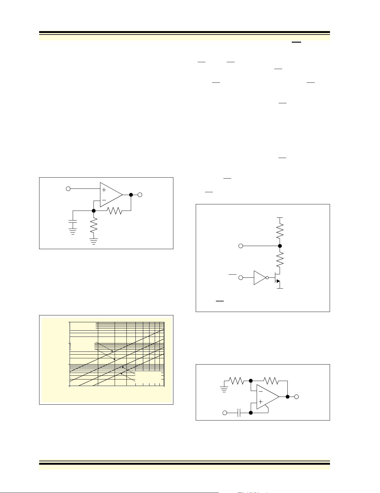
1. Non-inverting Gain and Unity-Gain Buffer.
a) Connect the guard ring to the inverting input
pin (V
common mode input voltage.
b) Connect the non-inverting pin (V
input with a wire that does not touch the
PCB surface.
2. Inverting (Figure 4-10) and Transimpedance
Gain Amplifiers (convert current to voltage, such
as photo detectors).
a) Connect the guard ring to the non-inverting
input pin (V
to the same reference voltage as the op
amp’s input (e.g., VDD/2 or ground).
b) Connect the inverting pin (VIN–) to the input
with a wire that does not touch the PCB
surface.
–); this biases the guard ring to the
IN
12
Ω. A 5V difference would
+) to the
IN
+). This biases the guard ring
IN
¼ MCP6144 (A) ¼ MCP6144 (B)
V
DD
V
DD
4.10 High Speed PCB Layout
Due to their speed capabilities, a little extra care in the
PCB (Printed Circuit Board) layout can make a
V
R
DD
significant difference in the performance of these op
amps. Good PC board layout techniques will help you
R
achieve the performance shown in Section 1.0 “Elec-
trical Characteristics” and Section 2.0 “Typical Performance Curves”, while also helping you minimize
EMC (Electro-Magnetic Compatibility) issues.
FIGURE 4-9: Unused Op Amps.
Use a solid ground plane and connect the bypass local
capacitor(s) to this plane with minimal length traces.
This cuts down inductive and capacitive crosstalk.
© 2006 Microchip Technology Inc. DS21685C-page 15
Page 16

MCP6021/1R/2/3/4
Separate digital from analog, low speed from high
speed and low power from high power. This will reduce
interference.
Keep sensitive traces short and straight. Separating
them from interfering components and traces. This is
especially important for high-frequency (low rise-time)
signals.
Sometimes it helps to place guard traces next to victim
traces. They should be on both sides of the victim
trace, and as close as possible. Connect the guard
trace to ground plane at both ends, and in the middle
for long traces.
Use coax cables (or low inductance wiring) to route
signal and power to and from the PCB.
4.11 Typical Applications
4.11.1 A/D CONVERTER DRIVER AND
ANTI-ALIASING FILTER
Figure 4-11 shows a third-order Butterworth filter that
can be used as an A/D converter driver. It has a bandwidth of 20 kHz and a reasonable step response. It will
work well for conversion rates of 80 ksps and greater (it
has 29 dB attenuation at 60 kHz).
4.11.2 OPTICAL DETECTOR AMPLIFIER
Figure 4-12 shows the MCP6021 op amp used as a
transimpedance amplifier in a photo detector circuit.
The photo detector looks like a capacitive current
source, so the 100 kΩ resistor gains the input signal to
a reasonable level. The 5.6 pF capacitor stabilizes this
circuit and produces a flat frequency response with a
bandwidth of 370 kHz.
Photo
Detector
100 pF
5.6 pF
100 kΩ
MCP6021
VDD/2
FIGURE 4-12: Transimpedance Amplifier for an Optical Detector.
1.0 nF
8.45 kΩ
1.2 nF
14.7 kΩ 33.2 kΩ
100 pF
MCP602X
FIGURE 4-11: A/D converter driver and
anti-aliasing filter with a 20 kHz cutoff frequency.
This filter can easily be adjusted to another bandwidth
by multiplying all capacitors by the same factor.
Alternatively, the resistors can all be scaled by another
common factor to adjust the bandwidth.
DS21685C-page 16 © 2006 Microchip Technology Inc.
Page 17

MCP6021/1R/2/3/4
5.0 DESIGN TOOLS
Microchip provides the basic design tools needed for
the MCP6021/1R/2/3/4 family of op amps.
5.1 SPICE Macro Model
The latest SPICE macro model available for the
MCP6021/1R/2/3/4 op amps is on Microchip’s web site
at www.microchip.com. This model is intended as an
initial design tool that works well in the op amp’s linear
region of operation at room temperature. Within the
macro model file is information on its capabilities.
Bench testing is a very important part of any design and
cannot be replaced with simulations. Also, simulation
results using this macro model need to be validated by
comparing them to the data sheet specifications and
characteristic curves.
5.2 FilterLab® Software
Microchip’s FilterLab® software is an innovative tool
that simplifies analog active filter (using op amps)
design. It is available free of charge from our web site
at www.microchip.com. The FilterLab software tool
provides full schematic diagrams of the filter circuit with
component values. It also outputs the filter circuit in
SPICE format, which can be used with the macro
model to simulate actual filter performance.
© 2006 Microchip Technology Inc. DS21685C-page 17
Page 18

MCP6021/1R/2/3/4
6.0 PACKAGING INFORMATION
6.1 Package Marking Information
5-Lead SOT-23 (MCP6021/MCP6021R)
Device E-Temp Code
XXNN EY25
8-Lead PDIP (300 mil)
XXXXXXXX
XXXXXNNN
YYWW
8-Lead SOIC (150 mil)
XXXXXXXX
XXXXYYWW
NNN
MCP6021 EYNN
MCP6021R EZNN
Note: Applies to 5-Lead SOT-23
Example:
MCP6021
I/P256
0331
Example:
MCP6021
I/SN0331
256
Example: (E-temp)
OR
OR
MCP6021
3
e
E/P^^256
0549
MCP6021E
3
e
SN^^0549
256
8-Lead MSOP
XXXXXX
YWWNNN
8-Lead TSSOP
XXXX
YYWW
NNN
Legend: XX...X Customer-specific information
Y Year code (last digit of calendar year)
YY Year code (last 2 digits of calendar year)
WW Week code (week of January 1 is week ‘01’)
NNN Alphanumeric traceability code
3
e
Pb-free JEDEC designator for Matte Tin (Sn)
* This package is Pb-free. The Pb-free JEDEC designator ( )
can be found on the outer packaging for this package.
Note: In the event the full Microchip part number cannot be marked on one line, it will
be carried over to the next line, thus limiting the number of available
characters for customer-specific information.
Example:
Example:
6021E
549256
6021
E549
256
3
e
DS21685C-page 18 © 2006 Microchip Technology Inc.
Page 19

Package Marking Information (Continued)
14-Lead PDIP (300 mil) (MCP6024) Example:
MCP6021/1R/2/3/4
XXXXXXXXXXXXXX
XXXXXXXXXXXXXX
YYWWNNN
14-Lead SOIC (150 mil) (MCP6024)
XXXXXXXXXX
XXXXXXXXXX
YYWWNNN
OR
OR
MCP6024-I/P
XXXXXXXXXXXXXX
Example:
0331256
MCP6024
E/P^^
3
e
0549256
MCP6024ISL
XXXXXXXXXX
0331256
MCP6024
E/SL^^
0549256
3
e
14-Lead TSSOP (MCP6024)
XXXXXX
YYWW
NNN
© 2006 Microchip Technology Inc. DS21685C-page 19
Example:
6024E
0331
256
Page 20

MCP6021/1R/2/3/4
5-Lead Plastic Small Outline Transistor (OT) (SOT-23)
E
E1
p
B
p1
D
n
c
β
Units
Number of Pins
Pitch
Outside lead pitch (basic)
Foot Angle
Lead Thickness
Mold Draft Angle Top
Mold Draft Angle Bottom
*
Controlling Parameter
Notes:
Dimensions D and E1 do not include mold flash or protrusions. Mold flash or protrusions shall not exceed .005" (0.127mm) per side.
EIAJ Equivalent: SC-74A
Drawing No. C04-091
p1
1
A
φ
L
n
p
f
c
a
b
A1
*
MILLIMETERSINCHES
0.95.038
1.90.075
Revised 09-12-05
A2
MAXNOMMINMAXNOMMINDimension Limits
55
1.451.180.90.057.046.035AOverall Height
1.301.100.90.051.043.035A2Molded Package Thickness
0.150.080.00.006.003.000A1Standoff
3.002.802.60.118.110.102EOverall Width
1.751.631.50.069.064.059E1Molded Package Width
3.102.952.80.122.116.110DOverall Length
0.550.450.35.022.018.014LFoot Length
0.200.150.09.008.006.004
0.500.430.35.020.017.014BLead Width
α
10501050
10501050
10501050
DS21685C-page 20 © 2006 Microchip Technology Inc.
Page 21
8-Lead Plastic Dual In-line (P) – 300 mil (PDIP)
E1
D
2
MCP6021/1R/2/3/4
n
E
β
eB
Number of Pins
Pitch
Top to Seating Plane A .140 .155 .170 3.56 3.94 4.32
Molded Package Thickness A2 .115 .130 .145 2.92 3.30 3.68
Base to Seating Plane A1 .015 0.38
Shoulder to Shoulder Width E .300 .313 .325 7.62 7.94 8.26
Molded Package Width E1 .240 .250 .260 6.10 6.35 6.60
Overall Length D .360 .373 .385 9.14 9.46 9.78
Tip to Seating Plane L .125 .130 .135 3.18 3.30 3.43
Lead Thickness
Upper Lead Width B1 .045 .058 .070 1.14 1.46 1.78
Lower Lead Width B .014 .018 .022 0.36 0.46 0.56
Overall Row Spacing § eB .310 .370 .430 7.87 9.40 10.92
Mold Draft Angle Top
Mold Draft Angle Bottom
* Controlling Parameter
§ Significant Characteristic
Notes:
Dimensions D and E1 do not include mold flash or protrusions. Mold flash or protrusions shall not exceed
.010” (0.254mm) per side.
JEDEC Equivalent: MS-001
Drawing No. C04-018
Dimension Limits MIN NOM MAX MIN NOM MAX
1
α
A
c
Units INCHES* MILLIMETERS
n
p
c
α
β
.008 .012 .015 0.20 0.29 0.38
A1
B1
B
88
.100 2.54
51015 51015
51015 51015
A2
L
p
© 2006 Microchip Technology Inc. DS21685C-page 21
Page 22

MCP6021/1R/2/3/4
8-Lead Plastic Small Outline (SN) – Narrow, 150 mil (SOIC)
E
E1
p
D
2
B
Number of Pins
Pitch
Foot Angle
Lead Thickness
Mold Draft Angle Top
Mold Draft Angle Bottom
* Controlling Parameter
§ Significant Characteristic
Notes:
Dimensions D and E1 do not include mold flash or protrusions. Mold flash or protrusions shall not exceed
.010” (0.254mm) per side.
JEDEC Equivalent: MS-012
Drawing No. C04-057
n
45°
c
β
n
p
φ
c
α
β
1
h
A
φ
L
048048
A1
MILLIMETERSINCHES*Units
1.27.050
α
A2
MAXNOMMINMAXNOMMINDimension Limits
88
1.751.551.35.069.061.053AOverall Height
1.551.421.32.061.056.052A2Molded Package Thickness
0.250.180.10.010.007.004A1Standoff §
6.206.025.79.244.237.228EOverall Width
3.993.913.71.157.154.146E1Molded Package Width
5.004.904.80.197.193.189DOverall Length
0.510.380.25.020.015.010hChamfer Distance
0.760.620.48.030.025.019LFoot Length
0.250.230.20.010.009.008
0.510.420.33.020.017.013BLead Width
1512015120
1512015120
DS21685C-page 22 © 2006 Microchip Technology Inc.
Page 23

MCP6021/1R/2/3/4
8-Lead Plastic Thin Shrink Small Outline (ST) – 4.4 mm (TSSOP)
E
E1
p
D
2
1
n
B
A
c
β
Number of Pins
Pitch
Foot Angle
Lead Thickness
Mold Draft Angle Top
Mold Draft Angle Bottom
*
Controlling Parameter
Notes:
Dimensions D and E1 do not include mold flash or protrusions. Mold flash or protrusions shall not exceed .005" (0.127mm) per side.
JEDEC Equivalent: MO-153
Drawing No. C04-086
L
n
p
φ
c
α
β
0° 4° 8° 0° 4° 8°
φ
INCHESUnits
A1
MILLIMETERS
A2
*
MAXNOMMINMAXNOMMINDimension Limits
88
0.65.026
1.101.051.00.043.041.039AOverall Height
0.950.900.85.037.035.033A2Molded Package Thickness
0.150.100.05.006.004.002A1Standoff
6.506.386.25.256.251.246EOverall Width
4.504.404.30.177.173.169E1Molded Package Width
3.103.002.90.122.118.114DMolded Package Length
0.700.600.50.028.024.020LFoot Length
0.200.150.09.008.006.004
0.300.250.19.012.010.007BLead Width
Revised 07-21-05
α
10°5°0°10°5°0°
10°5°0°10°5°0°
© 2006 Microchip Technology Inc. DS21685C-page 23
Page 24
MCP6021/1R/2/3/4
8-Lead Plastic Micro Small Outline Package (MS) (MSOP)
E
E1
p
D
2
n1
B
α
c
F
β
Units
Dimension Limits
Number of Pins
Pitch
Overall Height
Molded Package Thickness
Standoff
Overall Width
Molded Package Width
Overall Length
Foot Length
Foot Angle
Lead Thickness
Lead Width
Mold Draft Angle Top
Mold Draft Angle Bottom
*
Controlling Parameter
Notes:
Dimensions D and E1 do not include mold flash or protrusions. Mold flash or protrusions shall not exceed .010" (0.254mm) per side.
BSC: Basic Dimension. Theoretically exact value shown without tolerances.
See ASME Y14.5M
REF: Reference Dimension, usually without tolerance, for information purposes only.
See ASME Y14.5M
JEDEC Equivalent: MO-187
Drawing No. C04-111
n
p
A
A2
A1
E
E1
D
L
φ
c
B
α
β
MIN
.030
.000
.016 .024
0° - 8°
.003
.009
5°
5° -
L
INCHES
NOM
.026 BSC
.193 BSC
.118 BSC
.118 BSC
.037 REFFFootprint (Reference)
φ
8
--
.033
--
.006
.012
-
A
A1
MILLIMETERS
MAX NOM
.043
.037
.006
.031
.009
.016
15°
15°
MIN
0.65 BSC
-
0.75
0.00
4.90 BSC
3.00 BSC
3.00 BSC
0.40
0.95 REF
0°
0.08
0.22
*
8
-
0.85
0.60
-
-
-
Revised 07-21-05
A2
MAX
1.10
0.95
0.15
0.80
8°
0.23
0.40
15°5° 15°5° -
DS21685C-page 24 © 2006 Microchip Technology Inc.
Page 25

14-Lead Plastic Dual In-line (P) – 300 mil (PDIP)
E1
D
2
MCP6021/1R/2/3/4
n
E
β
eB
Number of Pins
Pitch
Top to Seating Plane A .140 .155 .170 3.56 3.94 4.32
Molded Package Thickness A2 .115 .130 .145 2.92 3.30 3.68
Base to Seating Plane A1 .015 0.38
Shoulder to Shoulder Width E .300 .313 .325 7.62 7.94 8.26
Molded Package Width
Overall Length D .740 .750 .760 18.80 19.05 19.30
Tip to Seating Plane L .125 .130 .135 3.18 3.30 3.43
Lead Thickness
Upper Lead Width B1 .045 .058 .070 1.14 1.46 1.78
Lower Lead Width B .014 .018 .022 0.36 0.46 0.56
Overall Row Spacing § eB .310 .370 .430 7.87 9.40 10.92
Mold Draft Angle Top
Mold Draft Angle Bottom
* Controlling Parameter
§ Significant Characteristic
Notes:
Dimensions D and E1 do not include mold flash or protrusions. Mold flash or protrusions shall not exceed
.010” (0.254mm) per side.
JEDEC Equivalent: MS-001
Drawing No. C04-005
1
A
c
A1
Dimension Limits MIN NOM MAX MIN NOM MAX
Units INCHES* MILLIMETERS
n
p
E1
c
α
β
.240 .250 .260 6.10 6.35 6.60
.008 .012 .015 0.20 0.29 0.38
5 10 15 5 10 15
5 10 15 5 10 15
B1
B
14 14
.100 2.54
α
A2
L
p
© 2006 Microchip Technology Inc. DS21685C-page 25
Page 26

MCP6021/1R/2/3/4
14-Lead Plastic Small Outline (SL) – Narrow, 150 mil (SOIC)
E
E1
p
D
2
B
n
1
45°
c
β
Number of Pins
Pitch
Foot Angle
Lead Thickness
Mold Draft Angle Top
Mold Draft Angle Bottom
* Controlling Parameter
§ Significant Characteristic
Notes:
Dimensions D and E1 do not include mold flash or protrusions. Mold flash or protrusions shall not exceed
.010” (0.254mm) per side.
JEDEC Equivalent: MS-012
Drawing No. C04-065
h
A
φ
L
n
p
φ
c
α
β
A1
048048
α
MILLIMETERSINCHES*Units
1.27.050
A2
MAXNOMMINMAXNOMMINDimension Limits
1414
1.751.551.35.069.061.053AOverall Height
1.551.421.32.061.056.052A2Molded Package Thickness
0.250.180.10.010.007.004A1Standoff §
6.205.995.79.244.236.228EOverall Width
3.993.903.81.157.154.150E1Molded Package Width
8.818.698.56.347.342.337DOverall Length
0.510.380.25.020.015.010hChamfer Distance
1.270.840.41.050.033.016LFoot Length
0.250.230.20.010.009.008
0.510.420.36.020.017.014BLead Width
1512015120
1512015120
DS21685C-page 26 © 2006 Microchip Technology Inc.
Page 27

MCP6021/1R/2/3/4
14-Lead Plastic Thin Shrink Small Outline (ST) – 4.4 mm (TSSOP)
E
E1
p
D
2
n
B
1
A
c
β
Number of Pins
Pitch
Foot Angle
Lead Thickness
Mold Draft Angle Top
Mold Draft Angle Bottom
*
Controlling Parameter
Notes:
Dimensions D and E1 do not include mold fla sh or protrusions. Mold flash or protrusions shall not exceed .005" (0.127mm) per side.
BSC: Basic Dimension. Theoretically exact value shown without tolerances.
See ASME Y14.5M
REF: Reference Dimension, usually without tole rance, for information purposes only.
See ASME Y14.5M
JEDEC Equivalent: MO-153 AB-1
Drawing No. C04-087
n
p
φ
c
α
β
0°
φ
L
INCHESUnits
12° REF
12° REF
MILLIMETERS
1414
0.65 BSC.026 BSC
12° REF
12° REF
Revised: 08-17-05
A2A1
*
MAXNOMMINMAXNOMMINDimension Limits
1.101.051.00.043.041.039AOverall Height
0.950.900.85.037.035.033A2Molded Package Thickness
0.150.100.05.006.004.002A1Standoff
6.506.386.25.256.251.246EOverall Width
4.504.404.30.177.173.169E1Molded Package Width
5.105.004.90.201.197.193DMolded Package Length
0.700.600.50.028.024.020LFoot Length
8°4°0°8°4°
0.200.150.09.008.006.004
0.300.250.19.012.010.007BLead Width
α
© 2006 Microchip Technology Inc. DS21685C-page 27
Page 28

MCP6021/1R/2/3/4
NOTES:
DS21685C-page 28 © 2006 Microchip Technology Inc.
Page 29

APPENDIX A: REVISION HISTORY
Revision C (March 2006)
The following is the list of modifications:
1. Added SOT-23-5 package option for single op
amps MCP6021 and MCP6021R (E-temp only).
2. Added MSOP-8 package option for E-temp
single op amp (MCP6021).
3. Corrected package drawing on front page for
dual op amp (MCP6022).
4. Clarified spec conditions (I
in Section 2.0 “Typical Performance
Curves”.
5. Added Section 3.0 “Pin Descriptions”.
6. Updated Section 4.0 “Applications informa-
tion” for THD+N, unused op amps, and gain
peaking discussions.
7. Corrected and updated package marking information in Section 6.0 “Packaging Informa-
tion”.
8. Added Appendix A: “REVISION HISTORY”.
, PM and THD+N)
SC
MCP6021/1R/2/3/4
Revision B (November 2003)
• Second Release of this Document
Revision A (November 2001)
• Original Release of this Document
© 2006 Microchip Technology Inc. DS21685C-page 29
Page 30

MCP6021/1R/2/3/4
NOTES:
DS21685C-page 30 © 2006 Microchip Technology Inc.
Page 31

MCP6021/1R/2/3/4
PRODUCT IDENTIFICATION SYSTEM
To order or obtain information, e.g., on pricing or delivery, refer to the factory or the listed sales office.
PART NO. X /XX
Device
PackageTemperature
Range
Device: MCP6021 Single Op Amp
Temperature Range: I = -40°C to +85°C
Package: OT = Plastic Small Outline Transistor (SOT-23), 5-lead
MCP6021T Single Op Amp
MCP6021R Single Op Amp
MCP6021RT Single Op Amp
MCP6022 Dual Op Amp
MCP6022T Dual Op Amp
MCP6023 Single Op Amp w/ CS
MCP6023T Single Op Amp w/ CS
MCP6024 Quad Op Amp
MCP6024T Quad Op Amp
E = -40°C to +125°C
MS = Plastic MSOP, 8-lead
P = Plastic DIP (300 mil Body), 8-lead, 14-lead
SN = Plastic SOIC (150mil Body), 8-lead
SL = Plastic SOIC (150 mil Body), 14-lead
ST = Plastic TSSOP, 8-lead
ST = Plastic TSSOP, 14-lead
(Tape and Reel for SOT-23, SOIC, TSSOP,
MSOP)
(Tape and Reel for SOT-23)
(Tape and Reel for SOIC and TSSOP)
(Tape and Reel for SOIC and TSSOP)
(Tape and Reel for SOIC and TSSOP)
(MCP6021, E-Temp; MCP6021R, E-Temp)
(MCP6021, E-Temp)
(MCP6021,I-Temp; MCP6022, I-Temp, E-Temp;
MCP6023, I-Temp, E-Temp;)
Examples:
a) MCP6021T-E/OT: Tape and Reel,
b) MCP6021-E/P: Extended temperature,
c) MCP6021-E/SN: Extended temperature,
a) MCP6021RT-E/OT:Tape and Reel,
a) MCP6022-I/P: Industrial temperature,
b) MCP6022-E/P: Extended temperature,
c) MCP6022T-E/ST: Tape and Reel,
a) MCP6023-I/P: Industrial temperature,
b) MCP6023-E/P: Extended temperature,
c) MCP6023-E/SN: Extended temperature,
a) MCP6024-I/SL: Industrial temperature,
b) MCP6024-E/SL: Extended temperature,
c) MCP6024T-E/ST: Tape and Reel,
Extended temperature,
5LD SOT-23.
8LD PDIP.
8LD SOIC.
Extended temperature,
5LD SOT-23.
8LD PDIP.
8LD PDIP.
Extended temperature,
8LD TSSOP.
8LD PDIP.
8LD PDIP.
8LD SOIC.
14LD SOIC.
14LD SOIC.
Extended temperature,
14LD TSSOP.
© 2006 Microchip Technology Inc. DS21685C-page 31
Page 32

MCP6021/1R/2/3/4
NOTES:
DS21685C-page 32 © 2006 Microchip Technology Inc.
Page 33

Note the following details of the code protection feature on Microchip devices:
• Microchip products meet the specification contained in their particular Microchip Data Sheet.
• Microchip believes that its family of products is one of the most secure families of its kind on the market today, when used in the
intended manner and under normal conditions.
• There are dishonest and possibly illegal methods used to breach the code protection feature. All of these methods, to our
knowledge, require using the Microchip products in a manner outside the operating specifications contained in Microchip’s Data
Sheets. Most likely, the person doing so is engaged in theft of intellectual property.
• Microchip is willing to work with the customer who is concerned about the integrity of their code.
• Neither Microchip nor any other semiconductor manufacturer can guarantee the security of their code. Code protection does not
mean that we are guaranteeing the product as “unbreakable.”
Code protection is constantly evolving. We at Microchip are committed to continuously improving the code protection features of our
products. Attempts to break Microchip’s code protection feature may be a violation of the Digital Millennium Copyright Act. If such acts
allow unauthorized access to your software or other copyrighted work, you may have a right to sue for relief under that Act.
Information contained in this publication regarding device
applications and the like is provided only for your convenience
and may be superseded by updates. It is your responsibility to
ensure that your application meets with your specifications.
MICROCHIP MAKES NO REPRESENTATIONS OR WARRANTIES OF ANY KIND WHETHER EXPRESS OR IMPLIED,
WRITTEN OR ORAL, STATUTORY OR OTHERWISE,
RELATED TO THE INFORMATION, INCLUDING BUT NOT
LIMITED TO ITS CONDITION, QUALITY, PERFORMANCE,
MERCHANTABILITY OR FITNESS FOR PURPOSE.
Microchip disclaims all liability arising from this information and
its use. Use of Microchip devices in life support and/or safety
applications is entirely at the buyer’s risk, and the buyer agrees
to defend, indemnify and hold harmless Microchip from any and
all damages, claims, suits, or expenses resulting from such
use. No licenses are conveyed, implicitly or otherwise, under
any Microchip intellectual property rights.
Trademarks
The Microchip name and logo, the Microchip logo, Accuron,
dsPIC, K
EELOQ, microID, MPLAB, PIC, PICmicro, PICSTART,
PRO MATE, PowerSmart, rfPIC, and SmartShunt are
registered trademarks of Microchip Technology Incorporated
in the U.S.A. and other countries.
AmpLab, FilterLab, Migratable Memory, MXDEV, MXLAB,
PICMASTER, SEEVAL, SmartSensor and The Embedded
Control Solutions Company are registered trademarks of
Microchip Technology Incorporated in the U.S.A.
Analog-for-the-Digital Age, Application Maestro, dsPICDEM,
dsPICDEM.net, dsPICworks, ECAN, ECONOMONITOR,
FanSense, FlexROM, fuzzyLAB, In-Circuit Serial
Programming, ICSP, ICEPIC, Linear Active Thermistor,
MPASM, MPLIB, MPLINK, MPSIM, PICkit, PICDEM,
PICDEM.net, PICLAB, PICtail, PowerCal, PowerInfo,
PowerMate, PowerTool, Real ICE, rfLAB, rfPICDEM, Select
Mode, Smart Serial, SmartTel, Total Endurance, UNI/O,
WiperLock and ZENA are trademarks of Microchip
Technology Incorporated in the U.S.A. and other countries.
SQTP is a service mark of Microchip Technology Incorporated
in the U.S.A.
All other trademarks mentioned herein are property of their
respective companies.
© 2006, Microchip Technology Incorporated, Printed in the
U.S.A., All Rights Reserved.
Printed on recycled paper.
Microchip received ISO/TS-16949:2002 quality system certification for
its worldwide headquarters, design and wafer fabrication facilities in
Chandler and Tempe, Arizona and Mountain View, California in
October 2003. The Company’s quality system processes and
procedures are for its PICmicro
devices, Serial EEPROMs, microperipherals, nonvolatile memory and
analog products. In addition, Microchip’s quality system for the design
and manufacture of development systems is ISO 9001:2000 certified.
®
8-bit MCUs, KEELOQ
®
code hopping
© 2006 Microchip Technology Inc. DS21685C-page 33
Page 34

WORLDWIDE SALES AND SERVICE
AMERICAS
Corporate Office
2355 West Chandler Blvd.
Chandler, AZ 85224-6199
Tel: 480-792-7200
Fax: 480-792-7277
Technical Support:
http://support.microchip.com
Web Address:
www.microchip.com
Atlanta
Alpharetta, GA
Tel: 770-640-0034
Fax: 770-640-0307
Boston
Westborough, MA
Tel: 774-760-0087
Fax: 774-760-0088
Chicago
Itasca, IL
Tel: 630-285-0071
Fax: 630-285-0075
Dallas
Addison, TX
Tel: 972-818-7423
Fax: 972-818-2924
Detroit
Farmington Hills, MI
Tel: 248-538-2250
Fax: 248-538-2260
Kokomo
Kokomo, IN
Tel: 765-864-8360
Fax: 765-864-8387
Los Angeles
Mission Viejo, CA
Tel: 949-462-9523
Fax: 949-462-9608
San Jose
Mountain View, CA
Tel: 650-215-1444
Fax: 650-961-0286
Toronto
Mississauga, Ontario,
Canada
Tel: 905-673-0699
Fax: 905-673-6509
ASIA/PACIFIC
Australia - Sydney
Tel: 61-2-9868-6733
Fax: 61-2-9868-6755
China - Beijing
Tel: 86-10-8528-2100
Fax: 86-10-8528-2104
China - Chengdu
Tel: 86-28-8676-6200
Fax: 86-28-8676-6599
China - Fuzhou
Tel: 86-591-8750-3506
Fax: 86-591-8750-3521
China - Hong Kong SAR
Tel: 852-2401-1200
Fax: 852-2401-3431
China - Qingdao
Tel: 86-532-8502-7355
Fax: 86-532-8502-7205
China - Shanghai
Tel: 86-21-5407-5533
Fax: 86-21-5407-5066
China - Shenyang
Tel: 86-24-2334-2829
Fax: 86-24-2334-2393
China - Shenzhen
Tel: 86-755-8203-2660
Fax: 86-755-8203-1760
China - Shunde
Tel: 86-757-2839-5507
Fax: 86-757-2839-5571
China - Wuhan
Tel: 86-27-5980-5300
Fax: 86-27-5980-5118
China - Xian
Tel: 86-29-8833-7250
Fax: 86-29-8833-7256
ASIA/PACIFIC
India - Bangalore
Tel: 91-80-4182-8400
Fax: 91-80-4182-8422
India - New Delhi
Tel: 91-11-5160-8631
Fax: 91-11-5160-8632
India - Pune
Tel: 91-20-2566-1512
Fax: 91-20-2566-1513
Japan - Yokohama
Tel: 81-45-471- 6166
Fax: 81-45-471-6122
Korea - Gumi
Tel: 82-54-473-4301
Fax: 82-54-473-4302
Korea - Seoul
Tel: 82-2-554-7200
Fax: 82-2-558-5932 or
82-2-558-5934
Malaysia - Penang
Tel: 60-4-646-8870
Fax: 60-4-646-5086
Philippines - Manila
Tel: 63-2-634-9065
Fax: 63-2-634-9069
Singapore
Tel: 65-6334-8870
Fax: 65-6334-8850
Taiwan - Hsin Chu
Tel: 886-3-572-9526
Fax: 886-3-572-6459
Taiwan - Kaohsiung
Tel: 886-7-536-4818
Fax: 886-7-536-4803
Taiwan - Taipei
Tel: 886-2-2500-6610
Fax: 886-2-2508-0102
Thailand - Bangkok
Tel: 66-2-694-1351
Fax: 66-2-694-1350
EUROPE
Austria - Wels
Tel: 43-7242-2244-399
Fax: 43-7242-2244-393
Denmark - Copenhagen
Tel: 45-4450-2828
Fax: 45-4485-2829
France - Paris
Tel: 33-1-69-53-63-20
Fax: 33-1-69-30-90-79
Germany - Munich
Tel: 49-89-627-144-0
Fax: 49-89-627-144-44
Italy - Milan
Tel: 39-0331-742611
Fax: 39-0331-466781
Netherlands - Drunen
Tel: 31-416-690399
Fax: 31-416-690340
Spain - Madrid
Tel: 34-91-708-08-90
Fax: 34-91-708-08-91
UK - Wokingham
Tel: 44-118-921-5869
Fax: 44-118-921-5820
02/16/06
DS21685C-page 34 © 2006 Microchip Technology Inc.
 Loading...