

Page 1

M
Rail-to-Rail Input/Output, 10 MHz Op Amps
MCP6021/2/3/4
Features
• Rail-to-Rail Input/Output
• Wide Bandwidth: 10 MHz (typ.)
• Low Noise: 8.7 nV/√Hz, at 10 kHz (typ.)
• Low Offset Voltage:
- Industrial Temperature: ±500 µV (max.)
- Extended Temperature: ±250 µV (max.)
• Mid-Supply V
• Low Supply Current: 1 mA (typ.)
• Total Harmonic Distortion: 0.00053% (typ., G = 1)
• Unity Gain Stable
• Power Supply Range: 2.5V to 5.5V
• Temperature Range:
- Industrial: -40°C to +85°C
- Extended: -40°C to +125°C
: MCP6021 and MCP6023
REF
Typical Applications
• Automotive
• Driving A/D Converters
• Multi-Pole Active Filters
• Barcode Scanners
• Audio Processing
• Communications
• DAC Buffer
• Test Equipment
• Medical Instrumentation
Description
The MCP6021, MCP6022, MCP6023 and MCP6024
from Microchip Technology Inc. are rail-to-rail input and
output op amps with high performance. Key
specifications include: wide bandwidth (10 MHz), low
noise (8.7 nV/√Hz), low input offset voltage and low
distortion (0.00053% THD+N). These features make
these op amps well suited for applications requiring
high performance and bandwidth. The MCP6023 also
offers a chip select pin (CS
when the part is not in use.
The single MCP6021, single MCP6023 and dual
MCP6022 are available in standard 8-lead PDIP, SOIC
and TSSOP. The quad MCP6024 is offered in 14-lead
PDIP, SOIC and TSSOP packages.
The MCP6021/2/3/4 family is available in the Industrial
and Extended temperature ranges. It has a power
supply range of 2.5V to 5.5V.
) that gives power savings
Available Tools
• SPICE Macro Model (at www.microchip.com)
• FilterLab
®
software (at www.microchip.com)
PACKAGE TYPES
MCP6021
PDIP SOIC, TSSOP
V
NC
1
–
V
2
IN
+
V
3
IN
V
4
SS
2003 Microchip Technology Inc. DS21685B-page 1
NC
8
V
7
V
6
V
5
DD
OUT
REF
OUTA
V
V
MCP6022
PDIP SOIC, TSSOP
1
–
2
INA
+
3
INA
V
4
SS
V
8
DD
V
7
OUTB
V
–
6
INB
+
V
5
INB
MCP6023
PDIP SOIC, TSSOP
NC
1
V
–
2
IN
+
V
3
IN
V
4
SS
DD
OUT
REF
V
V
V
V
V
V
OUTA
INA
INA
V
INB
INB
OUTB
CS
8
V
7
V
6
V
5
MCP6024
PDIP SOIC, TSSOP
DD
1
–
2
+
3
4
+
5
–
6
7
14
13
12
11
10
V
OUTD
V
–
IND
+
V
IND
V
SS
V
+
INC
–
V
9
INC
V
8
OUTC
Page 2
MCP6021/2/3/4
1.0 ELECTRICAL CHARACTERISTICS
Absolute Maximum Ratings †
VDD - VSS.........................................................................7.0V
All Inputs and Outputs ..................... V
Difference Input Voltage ....................................... |V
Output Short Circuit Current ..................................continuous
Current at Input Pins ....................................................±2 mA
Current at Output and Supply Pins ............................±30 mA
Storage Temperature ....................................-65°C to +150°C
Junction Temperature.................................................. +150°C
ESD Protection on all pins (HBM/MM)................ ≥ 2 kV / 200V
† Notice: Stresses above those listed under “Maximum
- 0.3V to VDD+0.3V
SS
DD-VSS
|
Pin Function Table
Name Function
VIN+, V
V
IN
V
DD
V
SS
CS
V
REF
V
OUT
V
OUTD
NC No Internal Connection
–, V
, V
INA
INA
OUTA
+, V
–, V
, V
INB
INB
OUTB
+, V
–, V
, V
Ratings” may cause permanent damage to the device. This is
a stress rating only and functional operation of the device at
those or any other conditions above those indicated in the
operational listings of this specification is not implied. Exposure to maximum rating conditions for extended periods may
affect device reliability.
DC CHARACTERISTICS
Electrical Specifications: Unless otherwise indicated, T
V
= VDD/2, V
CM
Parameters Sym Min Typ Max Units Conditions
Input Offset
Input Offset Voltage:
Industrial Temperature Parts V
Extended Temperature Parts V
Extended Temperature Parts V
Input Offset Voltage Temperature Drift ∆V
Power Supply Rejection Ratio PSRR 74 90 — dB V
Input Current and Impedance
Input Bias Current I
Industrial Temperature Parts I
Extended Temperature Parts I
Input Offset Current I
Common-Mode Input Impedance Z
Differential Input Impedance Z
Common-Mode
Common-Mode Input Range V
Common-Mode Rejection Ratio CMRR 74 90 — dB V
Voltage Reference (MCP6021 and MCP6023 only)
Accuracy (V
V
REF
Temperature Drift ∆V
V
REF
Open Loop Gain
DC Open Loop Gain (Large Signal) A
OUT
REF
≈ V
/2 and R
DD
- V
/2) ∆V
DD
=10kΩ to V
L
-500 — +500 µV VCM = 0V
-250 — +250 µV VCM = 0V, VDD = 5.0V
-2.5 — +2.5 mV VCM = 0V, VDD = 5.0V
A
VSS-0.3 — VDD+0.3 V
OS
OS
DIFF
CMR
OS
OS
OS
/∆T
B
B
B
CM
CMRR 70 85 — dB V
CMRR 74 90 — dB V
REF
/∆T
REF
A
OL
= +25°C, VDD = +2.5V to +5.5V, VSS = GND,
A
/2.
DD
—±3.5—µV/°CT
—1—pA
— 30 150 pA TA = +85°C
— 640 5,000 pA TA = +125°C
—±1—pA
—10
—10
13
||6 — Ω||pF
13
||3 — Ω||pF
-50 — +50 mV
—±100—µV/°CT
90 110 — dB VCM = 0V,
+, V
INC
INC
+ Non-inverting Inputs
IND
–, V
– Inverting Inputs
IND
Positive Power Supply
Negative Power Supply
Chip Select
Reference Voltage
,
OUTC
T
= -40°C to +125°C
A
= -40°C to +125°C
A
CM
DD
DD
DD
= -40°C to +125°C
A
V
OUT
Outputs
= 0V
= 5V, VCM = -0.3V to 5.3V
= 5V, VCM = 3.0V to 5.3V
= 5V, VCM = -0.3V to 3.0V
= VSS+0.3V to VDD-0.3V
DS21685B-page 2 2003 Microchip Technology Inc.
Page 3
MCP6021/2/3/4
DC CHARACTERISTICS (CONTINUED)
Electrical Specifications: Unless otherwise indicated, T
V
= VDD/2, V
CM
OUT
≈ V
/2 and R
DD
=10kΩ to V
L
DD
Parameters Sym Min Typ Max Units Conditions
Output
Maximum Output Voltage Swing V
Output Short Circuit Current I
OL
, V
SC
OHVSS
Power Supply
Supply Voltage V
Quiescent Current per Amplifier I
S
Q
2.5 — 5.5 V
0.5 1.0 1.35 mA IO = 0
AC CHARACTERISTICS
Electrical Specifications: Unless otherwise indicated, T
R
=10kΩ to V
L
/2 and CL = 60 pF.
DD
Parameters Sym Min Typ Max Units Conditions
AC Response
Gain Bandwidth Product GBWP — 10 — MHz
Phase Margin at Unity-Gain PM — 65 — ° G = 1
Settling Time, 0.2% t
SETTLE
Slew Rate SR — 7.0 — V/µs
Total Harmonic Distortion Plus Noise
f = 1 kHz, G = 1 THD+N — 0.00053 — % V
f = 1 kHz, G = 1, R
= 600Ω@1 KHz THD+N — 0.00064 — % V
L
f = 1 kHz, G = +1 V/V THD+N — 0.0014 — % V
f = 1 kHz, G = +10 V/V THD+N — 0.0009 — % V
f = 1 kHz, G = +100 V/V THD+N — 0.005 — % V
Noise
Input Voltage Noise E
Input Voltage Noise Density e
Input Current Noise Density i
ni
ni
ni
A
— 250 — ns G = 1, V
— 2.9 — µVp-p f = 0.1 Hz to 10 Hz
—8.7 —nV/√Hz f = 10 kHz
—3 —fA/√Hz f = 1 kHz
= +25°C, VDD = +2.5V to +5.5V, VSS = GND,
A
/2.
+15 — VDD-20 mV 0.5V output overdrive
—±30—mA
= 25°C, VDD = +2.5V to +5.5V, VSS = GND, VCM = VDD/2, V
OUT
OUT
OUT
OUT
OUT
≈ V
OUT
= 100 mV
OUT
p-p
= 0.25V + 3.25V, BW = 22 kHz
= 0.25V + 3.25V, BW = 22 kHz
= 4V
, VDD = 5.0V, BW = 22 kHz
P-P
= 4V
, VDD = 5.0V, BW = 22 kHz
P-P
= 4V
, VDD = 5.0V, BW = 22 kHz
P-P
DD
/2,
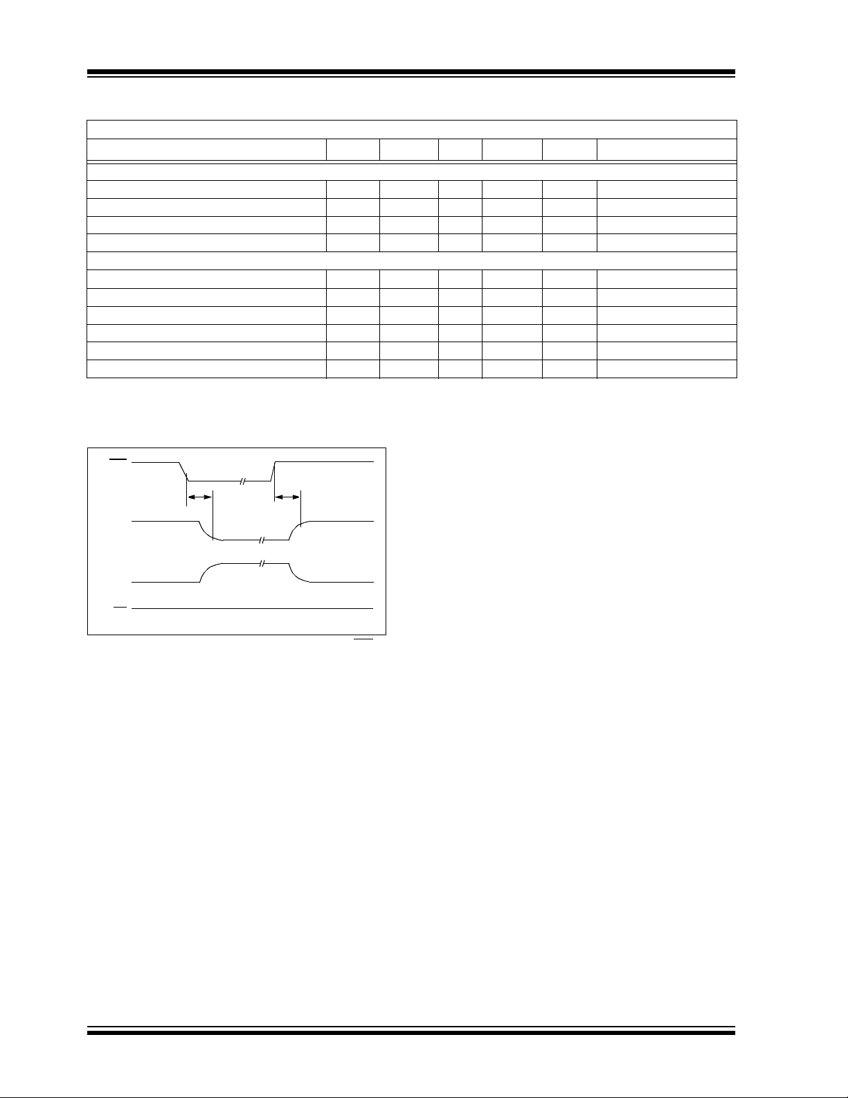
MCP6023 CHIP SELECT (CS) CHARACTERISTICS
Electrical Specifications: Unless otherwise indicated, T
R
=10kΩ to V
L
/2 and CL = 60 pF.
DD
= 25°C, VDD = +2.5V to +5.5V, VSS = GND, VCM = VDD/2, V
A
Parameters Sym Min Typ Max Units Conditions
DC Characteristics
Logic Threshold, Low
CS
CS Input Current, Low
CS Logic Threshold, High
CS Input Current, High
CS Input High, GND Current
Amplifier Output Leakage
V
IL
I
CSL
V
IH
I
CSH
I
SS
——0.01—µACS = V
0 — 0.2V
DD
V
-1.0 0.01 — µA CS = V
0.8V
—VDDV
DD
— 0.01 2.0 µA CS = V
— 0.05 2.0 µA CS = V
SS
DD
DD
DD
Timing
Low to Amplifier Output
CS
t
ON
Turn-on Time
CS High to Amplifier Output
t
OFF
High -Z Turn -off Time
Hysteresis
2003 Microchip Technology Inc. DS21685B-page 3
V
HYST
— 2 10 µs G = 1, VIN = VSS,
CS
= 0.2VDD to V
— 0.01 — µs G = 1, VIN = VSS,
CS
= 0.8VDD to V
— 0.6 — V Internal Switch
= 0.45VDD time
OUT
= 0.05VDD time
OUT
OUT
≈ V
DD
/2,
Page 4
MCP6021/2/3/4
TEMPERATURE CHARACTERISTICS
Electrical Specifications: Unless otherwise indicated, VDD = +2.5V to +5.5V and VSS = GND.
Parameters Symbol Min Typ Max Units Conditions
Temperature Ranges
Industrial Temperature Range T
Extended Temperature Range T
Operating Temperature Range T
Storage Temperature Range T
Thermal Package Resistances
Thermal Resistance, 8L-PDIP θ
Thermal Resistance, 8L-SOIC θ
Thermal Resistance, 8L-TSSOP θ
Thermal Resistance, 14L-PDIP θ
Thermal Resistance, 14L-SOIC θ
Thermal Resistance, 14L-TSSOP θ
A
A
A
A
JA
JA
JA
JA
JA
JA
Note 1: The industrial temperature devices operate over this extended temperature range, but with reduced
performance. In any case, the internal junction temperature (T
specification of 150°C.
-40 — +85 °C
-40 — +125 °C
-40 — +125 °C Note 1
-65 — +150 °C
—85—°C/W
—163— °C/W
—124— °C/W
—70—°C/W
—120— °C/W
—100— °C/W
) must not exceed the absolute maximum
J
CS
V
OUT
I
SS
I
CS
t
ON
Hi-Z
50 nA (typ.)
10 nA (typ.)
Amplifier On
1mA (typ.)
10 nA (typ.) 10 nA (typ.)
t
OFF
Hi-Z
50 nA (typ.)
FIGURE 1-1: Timing diagram for the CS pin on the MCP6023.
DS21685B-page 4 2003 Microchip Technology Inc.
Page 5

MCP6021/2/3/4
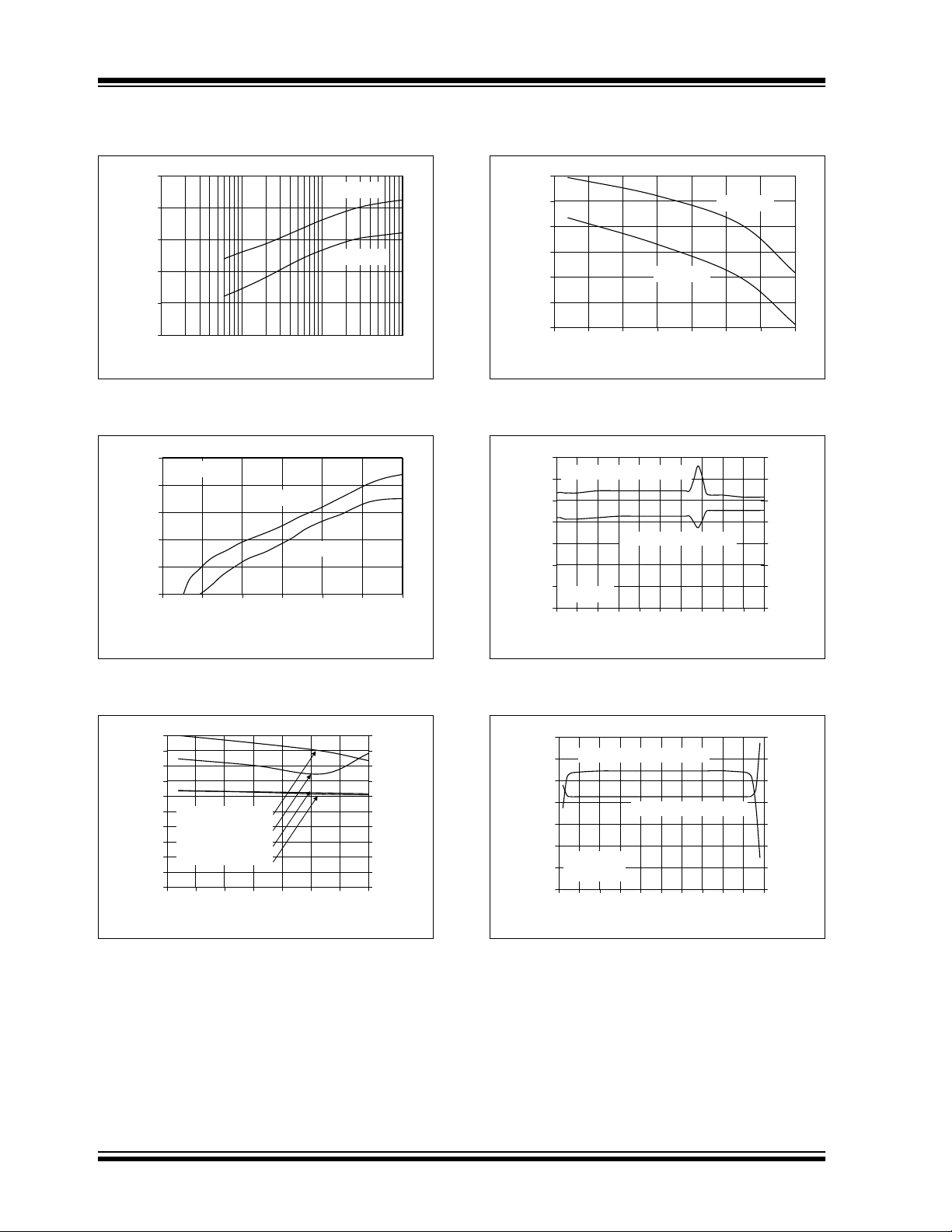
2.0 TYPICAL PERFORMANCE CURVES
Note: The graphs and tables provided following this note are a statistical summary based on a limited number of
samples and are provided for informational purposes only. The performance characteristics listed herein
are not tested or guaranteed. In some graphs or tables, the data presented may be outside the specified
operating range (e.g., outside specified power supply range) and therefore outside the warranted range.
Note: Unless otherwise indicated, T
V
≈ V
OUT
/2 and CL= 60 pF.
DD
16%
1192 Samples
14%
= +25°C
T
A
12%
10%
8%
6%
4%
2%
Percentage of Occurances
0%
-500
-400
-300
-200
Input Offset Voltage (µV)
-100
=+25°C, VDD= +2.5V to +5.5V, VSS= GND, VCM=VDD/2, R
A
0
100
200
300
FIGURE 2-1: Input Offset Voltage, (Industrial Temperature Parts).
24%
438 Samples
22%
20%
18%
16%
14%
12%
10%
Percentage of Occurances
8%
6%
4%
2%
0%
= 5.0V
V
DD
V
= 0V
CM
T
= +25°C
A
-200
-160
-80
-120
Input Offset Voltage (µV)
-40
0
40
E-Temp
80
120
I-Temp
Parts
400
Parts
160
500
200
=10kΩ to V
12%
1192 Samples
11%
TA = -40°C to +85°C
10%
9%
8%
7%
6%
5%
4%
3%
2%
1%
Percentage of Occurances
0%
-8-6-4
-12
-10
Input Offset Voltage Drift (µV/°C)
L
0
2
4
-2
6
I-Temp
Parts
8
DD
10
FIGURE 2-4: Input Offset Voltage Drift, (Industrial Temperature Parts).
26%
E-Temp
24%
22%
20%
18%
16%
14%
12%
10%
Percentage of Occurances
8%
6%
4%
2%
0%
Parts
-20
-16
-8
-12
Input Offset Voltage Drift (µV/°C)
0
-4
438 Samples
= 0V
V
CM
T
= -40°C to +125°C
A
4
8
12
16
/2,
12
20
FIGURE 2-2: Input Offset Voltage, (Extended Temperature Parts).
500
VDD = 2.5V
400
300
200
100
0
-100
-200
-300
Input Offset Voltage (µV)
-400
-500
-0.5 0.0 0.5 1.0 1.5 2.0 2.5 3.0
Common Mode Input Voltage (V)
-40°C
+25°C
+85°C
+125°C
FIGURE 2-3: Input Offset Voltage vs.
Common Mode Input Voltage with V
= 2.5V.
DD
FIGURE 2-5: Input Offset Voltage Drift, (Extended Temperature Parts).
500
VDD = 5.5V -40°C
400
300
200
100
0
-100
-200
-300
-400
Input Offset Voltage (µV)
-500
0.0
0.5
-0.5
1.0
Common Mode Input Voltage (V)
1.5
2.0
2.5
3.0
3.5
+25°C
+85°C
+125°C
4.0
4.5
5.0
5.5
FIGURE 2-6: Input Offset Voltage vs. Common Mode Input Voltage with VDD = 5.5V.
6.0
2003 Microchip Technology Inc. DS21685B-page 5
Page 6

MCP6021/2/3/4
Note: Unless otherwise indicated, T
V
≈ V
OUT
/2 and CL= 60 pF.
DD
100
50
0
-50
-100
-150
-200
VDD = 5.0V
-250
Input Offset Voltage (µV)
-300
= 0V
V
CM
-50 -25 0 25 50 75 100 125
Ambient Temperature (°C)
=+25°C, VDD= +2.5V to +5.5V, VSS= GND, VCM=VDD/2, R
A
FIGURE 2-7: Input Offset Voltage vs. Temperature.
1,000
100
Hz)
(nV/
10
Input Noise Voltage Density
1.E-01 1.E+00 1.E+01 1.E+02 1.E+03 1.E+04 1.E+05 1.E+06
1
0.1 1 10 100 1k 10k 1M100k
Frequency (Hz)
=10kΩ to V
L
200
VCM = VDD/2
150
100
50
0
-50
-100
-150
Input Offset Voltage (µV)
-200
VDD = 5.5V
VDD = 2.5V
0.0 0.5 1.0 1.5 2.0 2.5 3.0 3.5 4.0 4.5 5.0 5.5
Output Voltage (V)
FIGURE 2-10: Input Offset Voltage vs. Output Voltage.
16
f = 1 kHz
14
= 5.0V
V
DD
12
10
Hz)
8
(nV/
6
4
2
Input Noise Voltage Density
0
0.0
0.5
1.0
1.5
2.0
2.5
3.0
3.5
4.0
4.5
Common Mode Input Voltage (V)
DD
/2,
5.0
FIGURE 2-8: Input Noise Voltage Density vs. Frequency.
100
90
80
70
60
50
40
CMRR, PSRR (dB)
30
1.E+02 1.E+03 1.E+04 1.E+05 1.E+06
20
100 1k 10k 100k 1M
PSRR+
PSRR-
CMRR
Frequency (Hz)
FIGURE 2-9: Common Mode, Power Supply Rejection Ratios vs. Frequency.
FIGURE 2-11: Input Noise Voltage Density vs. Common Mode Input Voltage.
110
105
100
95
90
85
80
PSRR, CMRR (dB)
75
70
-50 -25 0 25 50 75 100 125
CMRR
PSRR (VCM = 0V)
Ambient Temperature (°C)
FIGURE 2-12: Common Mode, Power Supply Rejection Ratios vs. Temperature.
DS21685B-page 6 2003 Microchip Technology Inc.
Page 7

MCP6021/2/3/4
Note: Unless otherwise indicated, T
V
≈ V
OUT
/2 and CL= 60 pF.
DD
10,000
Input Bias, Offset Currents (pA)
VDD = 5.5V
1,000
100
10
1
0.0 0.5 1.0 1.5 2.0 2.5 3.0 3.5 4.0 4.5 5.0 5.5
Common Mode Input Voltage (V)
=+25°C, VDD= +2.5V to +5.5V, VSS= GND, VCM=VDD/2, R
A
IB, TA = +125°C
IOS, TA = +125°C
IB, TA = +85°C
IOS, TA = +85°C
FIGURE 2-13: Input Bias, Offset Currents vs. Common Mode Input Voltage.
1.2
1.1
1.0
0.9
0.8
0.7
0.6
0.5
0.4
(mA/amplifier)
0.3
Quiescent Current
0.2
0.1
0.0
0.0 0.5 1.0 1.5 2.0 2.5 3.0 3.5 4.0 4.5 5.0 5.5
Power Supply Voltage (V)
+125°C
+85°C
+25°C
-40°C
=10kΩ to V
10,000
VCM = V
DD
VDD = 5.5V
1,000
100
10
Input Bias, Offset Currents (pA)
1
25 35 45 55 65 75 85 95 105 115 125
Ambient Temperature (°C)
L
I
B
DD
I
OS
FIGURE 2-16: Input Bias, Offset Currents vs. Temperature.
1.2
1.1
VDD = 5.5V
1.0
0.9
0.8
0.7
0.6
0.5
0.4
(mA/amplifier)
0.3
Quiescent Current
0.2
VCM = VDD - 0.5V
0.1
0.0
-50 -25 0 25 50 75 100 125
VDD = 2.5V
Ambient Temperature (°C)
/2,
FIGURE 2-14: Quiescent Current vs. Supply Voltage.
35
30
25
20
(mA)
15
10
5
Output Short Circuit Current
0
0.0 0.5 1.0 1.5 2.0 2.5 3.0 3.5 4.0 4.5 5.0 5.5
+125°C
+85°C
+25°C
-40°C
Supply Voltage (V)
FIGURE 2-15: Output Short-Circuit Current vs. Supply Voltage.
FIGURE 2-17: Quiescent Current vs. Temperature.
120
110
100
90
80
70
60
50
40
30
20
10
Open-Loop Gain (dB)
0
-10
1.E+00 1.E+01 1.E+02 1.E+03 1.E+04 1.E+05 1.E+06 1.E+07 1.E+08
-20
1 10010 1k 100k10k 1M 100M10M
Frequency (Hz)
Gain
Phase
0
-15
-30
-45
-60
-75
-90
-105
-120
-135
-150
-165
Open-Loop Phase (°)
-180
-195
-210
FIGURE 2-18: Open-Loop Gain, Phase vs. Frequency.
2003 Microchip Technology Inc. DS21685B-page 7
Page 8
MCP6021/2/3/4
Note: Unless otherwise indicated, T
V
≈ V
OUT
/2 and CL= 60 pF.
DD
130
120
110
100
90
DC Open-Loop Gain (dB)
1.E+02 1.E+03 1.E+04 1.E+05
80
100 1k 10k 100k
Load Resistance (:)
=+25°C, VDD= +2.5V to +5.5V, VSS= GND, VCM=VDD/2, R
A
VDD = 5.5V
VDD = 2.5V
FIGURE 2-19: DC Open-Loop Gain vs. Load Resistance.
120
VCM = VDD/2
110
100
90
80
DC Open-Loop Gain (dB)
70
0.00 0.05 0.10 0.15 0.20 0.25 0.30
Output Voltage Headroom (V);
VDD = 5.5V
- VOH or VOL - V
V
DD
VDD = 2.5V
SS
=10kΩ to V
L
120
115
110
105
100
95
DC Open-Loop Gain (dB)
90
-50 -25 0 25 50 75 100 125
VDD = 2.5V
Ambient Temperature (°C)
VDD = 5.5V
FIGURE 2-22: DC Open-Loop Gain vs. Temperature.
14
Gain Bandwidth Product
12
10
8
(MHz)
6
4
2
Gain Bandwidth Product
VDD = 5.0V
0
0.0 0.5 1.0 1.5 2.0 2.5 3.0 3.5 4.0 4.5 5.0
Phase Margin, G = +1
Common Mode Input Voltage (V)
105
90
75
60
45
30
15
0
/2,
DD
Phase Margin, G = +1 (°)
FIGURE 2-20: Small Signal DC Open-Loop Gain vs. Output Voltage Headroom.
10
9
8
7
6
5
GBWP, VDD = 5.5V
(MHz)
4
GBWP, V
PM, V
3
PM, V
2
Gain Bandwidth Product
1
0
-50 -25 0 25 50 75 100 125
= 2.5V
DD
= 2.5V
DD
= 5.5V
DD
Ambient Temperature (°C)
100
90
80
70
60
50
40
30
20
Phase Margin, G = +1 (°)
10
0
FIGURE 2-21: Gain Bandwidth Product, Phase Margin vs. Temperature.
FIGURE 2-23: Gain Bandwidth Product, Phase Margin vs. Common Mode Input Voltage.
14
Gain Bandwidth Product
12
10
8
(MHz)
6
4
VDD = 5.0V
2
Gain Bandwidth Product
= VDD/2
V
CM
0
0.0 0.5 1.0 1.5 2.0 2.5 3.0 3.5 4.0 4.5 5.0
Phase Margin, G = +1
Output Voltage (V)
105
90
75
60
45
30
15
Phase Margin, G = +1 (°)
0
FIGURE 2-24: Gain Bandwidth Product, Phase Margin vs. Output Voltage.
DS21685B-page 8 2003 Microchip Technology Inc.
Page 9

MCP6021/2/3/4
Note: Unless otherwise indicated, T
V
≈ V
OUT
/2 and CL= 60 pF.
DD
11
Falling, VDD = 5.5V
10
Rising, V
9
8
7
6
5
4
3
Slew Rate (V/µs)
2
1
0
-50 -25 0 25 50 75 100 125
= 5.5V
DD
Falling, VDD = 2.5V
Rising, V
Ambient Temperature (°C)
=+25°C, VDD= +2.5V to +5.5V, VSS= GND, VCM=VDD/2, R
A
= 2.5V
DD
FIGURE 2-25: Slew Rate vs. Temperature.
0.1000%
0.0100%
THD+N (%)
0.0010%
0.0001%
G = +100 V/V
G = +10 V/V
G = +1 V/V
0.0 0.5 1.0 1.5 2.0 2.5 3.0 3.5 4.0 4.5 5.0
Output Voltage (V
f = 1 kHz
BW
Meas
= 5.0V
V
DD
= 22 kHz
)
P-P
=10kΩ to V
L
10
VDD = 5.5V
)
P-P
1
Swing (V
Maximum Output Voltage
1.E+04 1.E+05 1.E+06 1.E+07
0.1
10k 100k 1M 10M
VDD = 2.5V
Frequency (Hz)
DD
FIGURE 2-28: Maximum Output Voltage Swing vs. Frequency.
0.1000%
0.0100%
THD+N (%)
0.0010%
0.0001%
G = +100 V/V
G = +10 V/V
G = +1 V/V
0.0 0.5 1.0 1.5 2.0 2.5 3.0 3.5 4.0 4.5 5.0
Output Voltage (V
f = 20 kHz
= 80 kHz
BW
Meas
= 5.0V
V
DD
)
P-P
/2,
FIGURE 2-26: Total Harmonic Distortion plus Noise vs. Output Voltage with f = 1 kHz.
6
5
4
3
2
1
0
Input, Output Voltage (V)
0.0E+00 1.0E-05 2.0E-05 3.0E-05 4.0E-05 5.0E-05 6.0E-05 7.0E-05 8.0E-05 9.0E-05 1.0E-04
-1
V
V
OUT
Time (10 µs/div)
IN
VDD = 5V
G = +1 V/V
FIGURE 2-27: The MCP6021/2/3/4 family shows no phase reversal under overdrive.
FIGURE 2-29: Total Harmonic Distortion plus Noise vs. Output Voltage with f = 20 kHz.
135
130
125
120
(dB)
115
110
Channel to Channel Separation
G = +1 V/V
1.E+03 1.E+04 1.E+05 1.E+06
105
1k 1M
10k
Frequency (Hz)
100k
FIGURE 2-30: Channel-to-Channel Separation vs. Frequency (MCP6022 and MCP6024 only).
2003 Microchip Technology Inc. DS21685B-page 9
Page 10

MCP6021/2/3/4
Note: Unless otherwise indicated, T
V
≈ V
OUT
/2 and CL= 60 pF.
DD
=+25°C, VDD= +2.5V to +5.5V, VSS= GND, VCM=VDD/2, R
A
1,000
(mV)
SS
100
-V
OL
or V
10
OH
-V
DD
V
Output Voltage Headroom;
VOL - V
SS
VDD - V
OH
1
0.01 0.1 1 10
Output Current Magnitude (mA)
FIGURE 2-31: Output Voltage Headroom vs. Output Current.
6.E-02
5.E-02
4.E-02
3.E-02
2.E-02
1.E-02
0.E+00
-1.E-02
-2.E-02
-3.E-02
-4.E-02
Output Voltage (10 mV/div)
-5.E-02
-6.E-02
0.E+00 2.E-07 4.E-07 6.E-07 8.E-07 1.E-06 1.E-06 1.E-06 2.E-06 2.E-06 2.E-06
Time (200 ns/div)
G = +1 V/V
=10kΩ to V
10
9
8
(mV)
7
SS
-V
6
OL
5
4
or V
OH
3
-V
2
DD
V
1
Output Voltage Headroom
0
VOL - V
VDD - V
L
SS
OH
DD
-50 -25 0 25 50 75 100 125
Ambient Temperature (°C)
FIGURE 2-34: Output Voltage Headroom vs. Temperature.
6.E-02
5.E-02
4.E-02
3.E-02
2.E-02
1.E-02
0.E+00
-1.E-02
-2.E-02
-3.E-02
-4.E-02
Output Voltage (10 mV/div)
-5.E-02
-6.E-02
0.E+00 2.E-07 4.E-07 6.E-07 8.E-07 1.E-06 1.E-06 1.E-06 2.E-06 2.E-06 2.E-06
G = -1 V/V
= 1 k:
R
F
Time (200 ns/div)
/2,
FIGURE 2-32: Small-Signal Non-inverting Pulse Response.
5.0
4.5
4.0
3.5
3.0
2.5
2.0
1.5
Output Voltage (V)
1.0
0.5
0.E+00 5.E-07 1.E-06 2.E-06 2.E-06 3.E-06 3.E-06 4.E-06 4.E-06 5.E-06 5.E-06
0.0
Time (500 ns/div)
G = +1 V/V
FIGURE 2-33: Large-Signal Non-inverting Pulse Response.
FIGURE 2-35: Small-Signal Inverting Pulse Response.
5.0
4.5
4.0
3.5
3.0
2.5
2.0
1.5
Output Voltage (V)
1.0
0.5
0.E+00 5.E-07 1.E-06 2.E-06 2.E-06 3.E-06 3.E-06 4.E-06 4.E-06 5.E-06 5.E-06
0.0
G = -1 V/V
= 1 k:
R
F
Time (500 ns/div)
FIGURE 2-36: Large-Signal Inverting Pulse Response.
DS21685B-page 10 2003 Microchip Technology Inc.
Page 11

MCP6021/2/3/4
Note: Unless otherwise indicated, T
V
≈ V
OUT
FIGURE 2-37: V
/2 and CL= 60 pF.
DD
50
40
/2 (mV)
30
DD
20
-V
10
REF
0
-10
-20
-30
Accuracy; V
-40
REF
V
-50
0.0 0.5 1.0 1.5 2.0 2.5 3.0 3.5 4.0 4.5 5.0 5.5
Power Supply Voltage (V)
Accuracy vs. Supply
REF
=+25°C, VDD= +2.5V to +5.5V, VSS= GND, VCM=VDD/2, R
A
Voltage (MCP6021 and MCP6023 only).
1.6
Op Amp
1.4
turns on here
1.2
1.0
CS swept
0.8
high to low
0.6
VDD = 2.5V
(mA/amplifier)
0.4
Quiescent Current
G = +1 V/V
0.2
= 1.25V
V
IN
0.0
0.0 0.5 1.0 1.5 2.0 2.5
Chip Select Voltage (V)
Op Amp
shuts off here
Hysteresis
CS swept
low to high
=10kΩ to V
L
50
Representative Part
40
/2 (mV)
30
DD
20
-V
10
REF
0
-10
-20
-30
Accuracy; V
-40
REF
V
-50
-50 -25 0 25 50 75 100 125
Ambient Temperature (°C)
FIGURE 2-40: V
Accuracy vs.
REF
VDD = 5.5V
VDD = 2.5V
Temperature (MCP6021 and MCP6023 only).
1.6
Op Amp
1.4
turns on here
1.2
1.0
0.8
0.6
(mA/amplifier)
0.4
Quiescent Current
0.2
0.0
CS swept
high to low
VDD = 5.5V
G = +1 V/V
= 2.75V
V
IN
0.0 0.5 1.0 1.5 2.0 2.5 3.0 3.5 4.0 4.5 5.0 5.5
Chip Select Voltage (V)
Op Amp
shuts off here
Hysteresis
CS swept
low to high
DD
/2,
FIGURE 2-38: Chip Select (CS
(MCP6023 only) with V
5.5
5.0
4.5
4.0
3.5
3.0
2.5
2.0
1.5
Output
1.0
Output Voltage (V)
Chip Select Voltage,
on
0.5
0.0
0.0E+00 5.0E-06 1.0E-05 1.5E-05 2.0E-05 2.5E-05 3.0E-05 3.5E-05
-0.5
= 2.5V.
DD
CS Voltage
V
OUT
Output High-Z
Time (5 µs/div)
FIGURE 2-39: Chip Select (CS
) Hysteresis
VDD = 5.0V
G = +1 V/V
= V
V
IN
SS
Output
on
) to
Amplifier Output Response Time (MCP6023
only).
FIGURE 2-41: Chip Select (CS
(MCP6023 only) with V
= 5.5V.
DD
) Hysteresis
2003 Microchip Technology Inc. DS21685B-page 11
Page 12

MCP6021/2/3/4
3.0 APPLICATIONS INFORMATION
The MCP6021/2/3/4 family of operational amplifiers
are fabricated on Microchip’s state-of-the-art CMOS
process. They are unity-gain stable and suitable for a
wide range of general-purpose applications.
3.1 Rail-to-Rail Input
The MCP6021/2/3/4 amplifier family is designed to not
exhibit phase inversion when the input pins exceed the
supply voltages. Figure 2-27 shows an input voltage
exceeding both supplies with no resulting phase
inversion.
The input stage of the MCP6021/2/3/4 family of devices
uses two differential input stages in parallel; one
operates at low common-mode input voltage (V
while the other operates at high V
the device operates with V
supply rail (V
- 0.3V to V
SS
CM
. With this topology,
CM
up to 0.3V past either
+ 0.3V) at 25°C. The
DD
amplifier input behaves linearly as long as V
within the specified V
is measured at both V
limits. The input offset voltage
CMR
CM=VSS
- 0.3V and V
to ensure proper operation.
Input voltages that exceed the input voltage range
(V
) can cause excessive current to flow in or out of
CMR
the input pins. Current beyond ±2 mA introduces
possible reliability problems. Thus, applications that
exceed this rating must externally limit the input current
with an input resistor (R
), as shown in Figure 3-1.
IN
CM
DD
CM
is kept
+ 0.3V
3.3 MCP6023 Chip Select (CS)
The MCP6023 is a single amplifier with chip select
(CS
). When CS is high, the supply current is less than
10 nA (typ) and travels from the CS
pin to VSS, with the
amplifier output being put into a high-impedance state.
When CS
is low, the amplifier is enabled. If CS is left
floating, the amplifier will not operate properly.
Figure 1-1 and Figure 2-39 show the output voltage
and supply current response to a CS
pulse.
3.4 MCP6021 and MCP6023 Reference
Volta g e
The single op amps (MCP6021 and MCP6023) have
an internal mid-supply reference voltage connected to
),
the V
internally tied to VSS, which always keeps the op amp
on and always provides a mid-supply reference. With
the MCP6023, taking the CS
by shutting down both the op amp and the V
circuitry. Taking the CS pin low turns on the op amp and
V
REF
pin (see Figure 3-2). The MCP6021 has CS
REF
pin high conserves power
circuitry.
V
DD
50 kΩ
V
REF
REF
R
IN
V
IN
MCP602X
(Maximum expected V
≥
R
IN
- (Minimum expected VIN)
V
R
SS
≥
IN
FIGURE 3-1: R
IN
2mA
2mA
limits the current flow
IN
) - V
DD
V
OUT
into an input pin.
3.2 Rail-to-Rail Output
The Maximum Output Voltage Swing is the maximum
swing possible under a particular output load.
According to the specification table, the output can
reach within 20 mV of either supply rail when
R
=10kΩ. See Figure 2-31 and Figure 2-34 for more
L
information concerning typical performance.
50 kΩ
CS
V
SS
tied internally to VSS for MCP6021)
(CS
FIGURE 3-2: Simplified internal V
REF
circuit (MCP6021 and MCP6023 only).
See Figure 3-3 for a non-inverting gain circuit using the
internal mid-supply reference. The DC-blocking
capacitor (C
) also reduces noise by coupling the op
B
amp input to the source.
R
G
C
B
V
IN
R
F
V
OUT
V
REF
FIGURE 3-3: Non-inverting gain circuit
using V
(MCP6021 and MCP6023 only).
REF
DS21685B-page 12 2003 Microchip Technology Inc.
Page 13

To use the internal mid-supply reference for an
inverting gain circuit, connect the V
pin to the non-
REF
inverting input, as shown in Figure 3-4. The capacitor
C
helps reduce power supply noise on the output.
B
)
:
(
ISO
1,000
MCP6021/2/3/4
GN t +1
R
G
V
IN
R
F
V
OUT
V
REF
C
B
FIGURE 3-4: Inverting gain circuit using
V
(MCP6021 and MCP6023 only).
REF
If you don’t need the mid-supply reference, leave the
V
pin open.
REF
3.5 Capacitive Loads
Driving large capacitive loads can cause stability
problems for voltage feedback op amps. As the load
capacitance increases, the feedback loop’s phase
margin decreases, and the closed loop bandwidth is
reduced. This produces gain-peaking in the frequency
response, with overshoot and ringing in the step
response.
When driving large capacitive loads with these op
amps (e.g., > 60 pF when G = +1), a small series
resistor at the output (R
feedback loop’s phase margin (stability) by making the
load resistive at higher frequencies. The bandwidth will
be generally lower than the bandwidth with no
capacitive load.
V
IN
MCP602X
FIGURE 3-5: Output resistor R
stabilizes large capacitive loads.
Figure 3-6 gives recommended R
different capacitive laods and gains. The x-axis is the
normalized load capacitance (C
circuit’s noise gain. For non-inverting gains, G
gain are equal. For inverting gains, G
-1 V/V gives G
= +2 V/V).
N
in Figure 3-5) improves the
ISO
R
ISO
C
L
ISO
values for
ISO
), where GN is the
L/GN
is 1+|Gain| (e.g.,
N
N
V
OUT
and the
100
Recommended R
10
10 100 1,000 10,000
Normalized Capacitance; C
FIGURE 3-6: Recommended R
L/GN
(pF)
ISO
values
for capacitive loads.
After selecting R
resulting frequency response peaking and step
response overshoot. Evaluation on the bench and
simulations with the MCP6021/2/3/4 Spice macro
model are very helpful. Modify R
response is reasonable.
for your circuit, double-check the
ISO
’s value until the
ISO
3.6 Supply Bypass
With this family of operational amplifiers, the power
supply pin (V
for single supply) should have a local
DD
bypass capacitor (i.e., 0.01 µF to 0.1 µF) within 2 mm
for good, high-frequency performance. It also needs a
bulk capacitor (i.e., 1 µF or larger) within 100 mm to
provide large, slow currents. This bulk capacitor can be
shared with other parts.
3.7 PCB Surface Leakage
In applications where low input bias current is critical,
PCB (printed circuit board) surface-leakage effects
need to be considered. Surface leakage is caused by
humidity, dust or other contamination on the board.
Under low humidity conditions, a typical resistance
between nearby traces is 10
cause 5 pA of current to flow, which is greater than the
MCP6021/2/3/4 family’s bias current at 25°C (1 pA,
typ).
The easiest way to reduce surface leakage is to use a
guard ring around sensitive pins (or traces). The guard
ring is biased at the same voltage as the sensitive pin.
An example of this type of layout is shown in Figure 3-7.
Guard Ring VIN–VIN+
12
Ω. A 5V difference would
FIGURE 3-7: Example guard ring layout.
2003 Microchip Technology Inc. DS21685B-page 13
Page 14
MCP6021/2/3/4
1. Inverting (Figure 3-7) and Transimpedance
Gain Amplifiers (convert current to voltage, such
as photo detectors).
a. Connect the guard ring to the non-inverting
input pin (V
to the same reference voltage as the op
amp’s input (e.g., V
b. Connect the inverting pin (V
with a wire that does not touch the PCB
surface.
2. Non-inverting Gain and Unity-Gain Buffer
a. Connect the guard ring to the inverting input
pin (V
common mode input voltage.
b. Connect the non-inverting pin (V
input with a wire that does not touch the
PCB surface.
+). This biases the guard ring
IN
/2 or ground).
DD
–) to the input
IN
–); this biases the guard ring to the
IN
+) to the
IN
3.8 High-Speed PCB Layout
Due to their speed capabilities, a little extra care in the
PCB (Printed Circuit Board) layout can make a
significant difference in the performance of these op
amps. Good PC board layout techniques will help you
achieve the performance shown in the Electrical
Characteristics and Typical Performance Curves, while
also helping you minimize EMC (Electro-Magnetic
Compatibility) issues.
Use a solid ground plane and connect the bypass local
capacitor(s) to this plane with minimal length traces.
This cuts down inductive and capacitive crosstalk.
Separate digital from analog, low-speed from highspeed and low power from high power. This will reduce
interference.
Keep sensitive traces short and straight. Separating
them from interfering components and traces. This is
especially important for high-frequency (low rise-time)
signals.
Sometimes it helps to place guard traces next to victim
traces. They should be on both sides of the victim
trace, and as close as possible. Connect the guard
trace to ground plane at both ends, and in the middle
for long traces.
Use coax cables (or low inductance wiring) to route
signal and power to and from the PCB.
3.9 Typical Applications
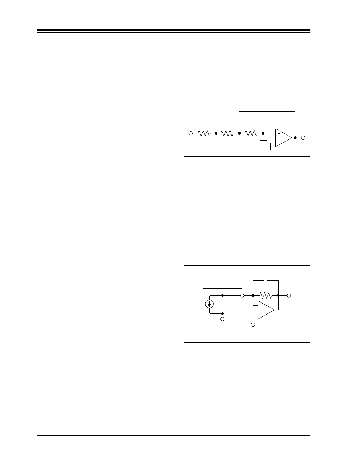
3.9.1 A/D CONVERTER DRIVER AND
ANTI-ALIASING FILTER
Figure 3-8 shows a third-order Butterworth filter that
can be used as an A/D converter driver. It has a bandwidth of 20 kHz and a reasonable step response. It will
work well for conversion rates of 80 ksps and greater (it
has 29 dB attenuation at 60 kHz).
1.0 nF
8.45 kΩ
1.2 nF
14.7 kΩ 33.2 kΩ
100 pF
FIGURE 3-8: A/D converter driver and
anti-aliasing filter with a 20 kHz cutoff frequency.
This filter can easily be adjusted to another bandwidth
by multiplying all capacitors by the same factor.
Alternatively, the resistors can all be scaled by another
common factor to adjust the bandwidth.
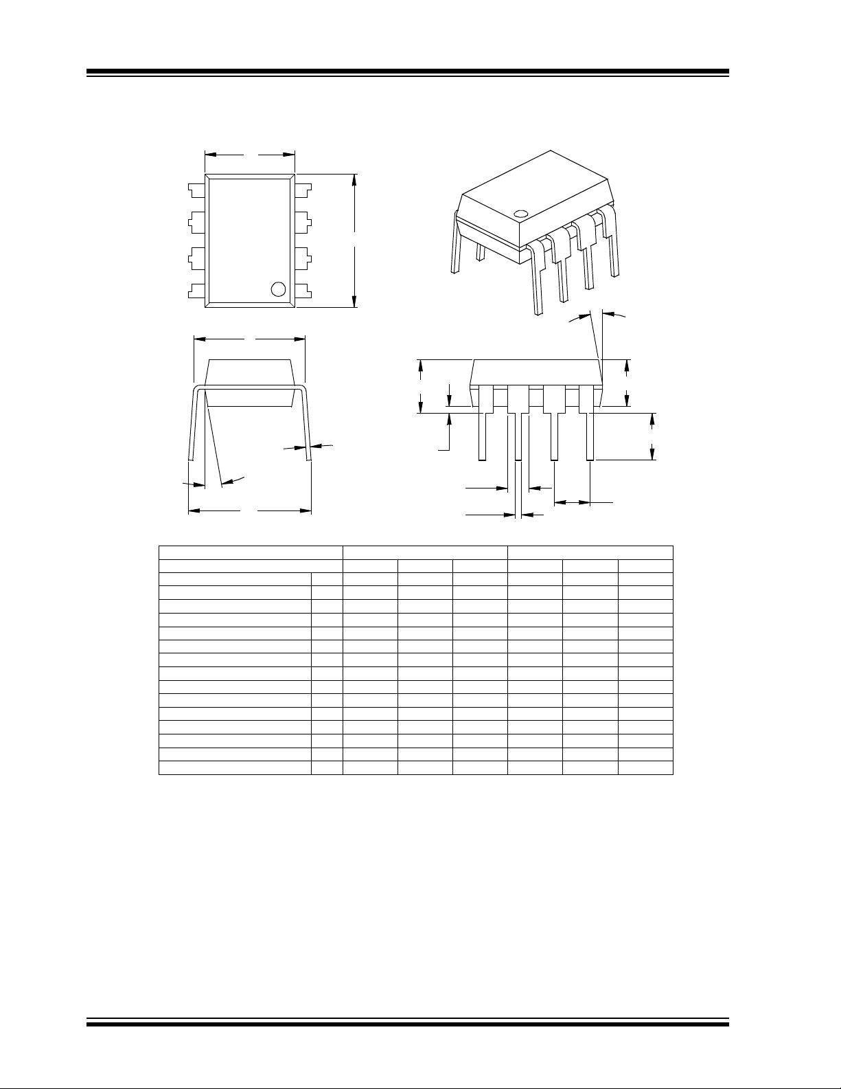
3.9.2 OPTICAL DETECTOR AMPLIFIER
Figure 3-9 shows the MCP6021 op amp used as a
transimpedance amplifier in a photo detector circuit.
The photo detector looks like a capacitive current
source, so the 100 kΩ resistor gains the input signal to
a reasonable level. The 5.6 pF capacitor stabilizes this
circuit and produces a flat frequency response with a
bandwidth of 370 kHz.
Photo
Detector
100 pF
V
DD
FIGURE 3-9: Transimpedance amplifier for an optical detector.
MCP602X
5.6 pF
100 kΩ
MCP6021
/2
DS21685B-page 14 2003 Microchip Technology Inc.
Page 15

4.0 DESIGN TOOLS
Microchip provides the basic design tools needed for
the MCP6021/2/3/4 family of op amps.
4.1 SPICE Macro Model
The latest SPICE macro model for the MCP6021/2/3/4
op amps is available on our web site
(www.microchip.com). This model is intended as an
initial design tool that works well in the op amp’s linear
region of operation at room temperature. See the
model file for information on its capabilities.
Bench testing is a very important part of any design and
cannot be replaced with simulations. Also, simulation
results using this macro model need to be validated by
comparing them to the data sheet specs and plots.
4.2 FilterLab® Software
The FilterLab® software is an innovative tool that
simplifies analog active filter (using op amps) design.
Available at no cost from our web site (at www.microchip.com), the FilterLab software active filter design
tool provides full schematic diagrams of the filter circuit
with component values. It also outputs the filter circuit
in SPICE format, which can be used with the Macro
Model to simulate actual filter performance.
MCP6021/2/3/4
2003 Microchip Technology Inc. DS21685B-page 15
Page 16

MCP6021/2/3/4
5.0 PACKAGING INFORMATION
5.1 Package Marking Information
8-Lead PDIP (300 mil)
XXXXXXXX
XXXXXNNN
YYWW
8-Lead SOIC (150 mil)
XXXXXXXX
XXXXYYWW
NNN
8-Lead TSSOP
XXXX
YWW
NNN
Example:
MCP6021
I/P256
0331
Example:
MCP6021
I/SN0331
256
Example:
6021
E331
256
Legend: XX...X Customer specific information*
Y Year code (last digit of calendar year)
YY Year code (last 2 digits of calendar year)
WW Week code (week of January 1 is week ‘01’)
NNN Alphanumeric traceability code
Note: In the event the full Microchip part number cannot be marked on one line, it will
be carried over to the next line thus limiting the number of available characters
for customer specific information.
* Standard device marking consists of Microchip part number, year code, week code, and traceability
code.
DS21685B-page 16 2003 Microchip Technology Inc.
Page 17

Package Marking Information (Continued)
14-Lead PDIP (300 mil) (MCP6024) Example:
MCP6021/2/3/4
XXXXXXXXXXXXXX
XXXXXXXXXXXXXX
YYWWNNN
14-Lead SOIC (150 mil) (MCP6024)
XXXXXXXXXX
XXXXXXXXXX
YYWWNNN
14-Lead TSSOP (MCP6024)
XXXXXX
YYWW
NNN
MCP6024-I/P
XXXXXXXXXXXXXX
0331256
Example:
MCP6024ISL
XXXXXXXXXX
0331256
Example:
6024E
0331
256
2003 Microchip Technology Inc. DS21685B-page 17
Page 18
MCP6021/2/3/4
8-Lead Plastic Dual In-line (P) – 300 mil (PDIP)
E1
D
2
n
E
β
eB
Number of Pins
Pitch
Top to Seating Plane A .140 .155 .170 3.56 3.94 4.32
Molded Package Thickness A2 .115 .130 .145 2.92 3.30 3.68
Base to Seating Plane A1 .015 0.38
Shoulder to Shoulder Width E .300 .313 .325 7.62 7.94 8.26
Molded Package Width E1 .240 .250 .260 6.10 6.35 6.60
Overall Length D .360 .373 .385 9.14 9.46 9.78
Tip to Seating Plane L .125 .130 .135 3.18 3.30 3.43
Lead Thickness
Upper Lead Width B1 .045 .058 .070 1.14 1.4 6 1.78
Lower Lead Width B .014 .018 .022 0.36 0.46 0.56
Overall Row Spacing § eB .310 .370 .430 7.87 9.40 10.92
Mold Draft Angle Top
Mold Draft Angle Bottom
* Controlling Parameter
§ Significant Characteristic
Notes:
Dimensions D and E1 do not include m old flash or protrusions. Mold flash or protrusions shall not exceed
.010” (0.254mm) per side.
JEDEC Equivalent: MS-001
Drawing No. C04-018
Dimension Limits MIN NOM MAX MIN NOM MAX
1
α
A
c
Units INCHES* MILLIMETERS
n
p
c
α
β
.008 .012 .015 0.20 0.29 0.38
A1
B1
B
88
.100 2.54
51015 51015
51015 51015
A2
L
p
DS21685B-page 18 2003 Microchip Technology Inc.
Page 19
8-Lead Plastic Small Outline (SN) – Narrow, 150 mil (SOIC)
E
E1
p
D
2
MCP6021/2/3/4
B
Number of Pins
Pitch
Foot Angle
Lead Thickness
Mold Draft Angle Top
Mold Draft Angle Bottom
* Controlling Paramete r
§ Significant Characteristic
Notes:
Dimensions D and E1 do not include mold flash or protrusions. Mold flash or protrusions shall not exceed
.010” (0.254mm) per side.
JEDEC Equivalent: MS-012
Drawing No. C04-057
n
45°
c
β
n
p
φ
c
α
β
1
h
A
φ
L
048048
A1
MILLIMETERSINCHES*Units
1.27.050
α
A2
MAXNOMMINMAXNOMMINDimension Limits
88
1.751.551.35.069.061.053AOverall Height
1.551.421.32.061.056.052A2Molded Package Thickness
0.250.180.10.010.007.004A1Standoff §
6.206.025.79.244.237.228EOverall Width
3.993.913.71.157.154.146E1Molded Package W idth
5.004.904.80.197.193.189DOverall Length
0.510.380.25.020.015.010hChamfer Distance
0.760.620.48.030.025.019LFoot Length
0.250.230.20.010.009.008
0.510.420.33.020.017.013BLead Width
1512015120
1512015120
2003 Microchip Technology Inc. DS21685B-page 19
Page 20

MCP6021/2/3/4
8-Lead Plastic Thin Shrink Small Outline (ST) – 4.4 mm (TSSOP)
E
E1
p
D
2
n
B
1
A
c
A1
φ
β
Number of Pins
Pitch
Foot Angle
Lead Thickness
Mold Draft Angle Top
Mold Draft Angle Bottom
* Controlling Parameter
§ Significant Cha racteristic
Notes:
Dimensions D and E1 do not include mold flash or protrusions. Mold flash or protrusions shall not exceed
.005” (0.127mm) per side.
JEDEC Equivalent: MO-153
Drawing No. C04-086
n
p
φ
c
α
β
048048
L
MILLIMETERS*INCHESUnits
0.65.026
α
A2
MAXNOMMINMAXNOMMINDimension Limits
88
1.10.043AOverall Height
0.950.900.85.037.035.033A2Molded Package Thickness
0.150.100.05.006.004.002A1Standoff §
6.506.386.25.256.251.246EOverall Width
4.504.404.30.177.173.169E1Molded Package Width
3.103.002.90.122.118.114DMolded Package Length
0.700.600.50.028.024.020LFoot Len gth
0.200.150.09.008.006.004
0.300.250.19.012.010.007BLead Width
10501050
10501050
DS21685B-page 20 2003 Microchip Technology Inc.
Page 21

14-Lead Plastic Dual In-line (P) – 300 mil (PDIP)
E1
D
2
MCP6021/2/3/4
n
E
β
eB
Number of Pins
Pitch
Top to Seating Plane A .140 .155 .170 3.56 3.94 4.32
Molded Package Thickness A2 .115 .130 .145 2.92 3.30 3.68
Base to Seating Plane A1 .015 0.38
Shoulder to Shoulder Width E .300 .313 .325 7.62 7.94 8.26
Molded Package Width E1 .240 .250 .260 6.10 6.35 6.60
Overall Length D .740 .750 .760 18.80 19.05 19.30
Tip to Seating Plane L .125 .130 .135 3.18 3.30 3.43
Lead Thickness
Upper Lead Width B1 .045 .058 .070 1.14 1.4 6 1.78
Lower Lead Width B .014 .018 .022 0.36 0.46 0.56
Overall Row Spacing § eB .310 .370 .430 7.87 9.40 10.92
Mold Draft Angle Top
Mold Draft Angle Bottom
* Controlling Parameter
§ Significant Characteristic
Notes:
Dimensions D and E1 do not include m old flash or protrusions. Mold flash or protrusions shall not exceed
.010” (0.254mm) per side.
JEDEC Equivalent: MS-001
Drawing No. C04-005
1
A
c
A1
Dimension Limits MIN NOM MAX MIN NOM MAX
Units INCHES* MILLIMETERS
n
p
c
α
β
.008 .012 .015 0.20 0.29 0.38
5 10 1 5 5 10 15
5 10 1 5 5 10 15
B1
B
14 14
.100 2.54
α
A2
L
p
2003 Microchip Technology Inc. DS21685B-page 21
Page 22

MCP6021/2/3/4
14-Lead Plastic Small Outline (SL) – Narrow, 150 mil (SOIC)
E
E1
p
D
2
B
n
1
45°
c
β
Number of Pins
Pitch
Foot Angle
Lead Thickness
Mold Draft Angle Top
Mold Draft Angle Bottom
* Controlling Paramete r
§ Significant Characteristic
Notes:
Dimensions D and E1 do not include mold flash or protrusions. Mold flash or protrusions shall not exceed
.010” (0.254mm) per side.
JEDEC Equivalent: MS-012
Drawing No. C04-065
h
A
φ
L
n
p
φ
c
α
β
A1
048048
α
MILLIMETERSINCHES*Units
A2
MAXNOMMINMAXNOMMINDimension Limits
1414
1.27.050
1.751.551.35.069.061.053AOverall Height
1.551.421.32.061.056.052A2Molded Package Thickness
0.250.180.10.010.007.004A1Standoff §
6.205.995.79.244.236.228EOverall Width
3.993.903.81.157.154.150E1Molded Package Width
8.818.698.56.347.342.337DOverall Len gth
0.510.380.25.020.015.010hChamfer Distance
1.270.840.41.050.033.016LFoot Len gth
0.250.230.20.010.009.008
0.510.420.36.020.017.014BLead Width
1512015120
1512015120
DS21685B-page 22 2003 Microchip Technology Inc.
Page 23
MCP6021/2/3/4
14-Lead Plastic Thin Shrink Small Outline (ST) – 4.4 mm (TSSOP)
E
E1
p
D
2
n
B
1
A
c
φ
β
Number of Pins
Pitch
Foot Angle
Lead Thickness
Mold Draft Angle Top
Mold Draft Angle Bottom
* Controlling Parameter
§ Significant Characteristic
Notes:
Dimensions D and E1 do not include mo ld flash or protrusions. Mold flash or protrusions shall not exceed
.005” (0.127mm) per side.
JEDEC Equivalent: MO-153
Drawing No. C04-087
n
p
φ
c
α
β
L
MILLIMETERS*INCHESUnits
0.65.026
α
A2A1
MAXNOMMINMAXNOMMINDimension Limits
1414
1.10.043AOverall Height
0.950.900.85.037.035.033A2Molded Package Thickness
0.150.100.05.006.004.002A1Standoff §
6.506.386.25.256.251.246EOverall Width
4.504.404.30.177.173.169E1Molded Package Width
5.105.004.90.201.197.193DMolded Package Length
0.700.600.50.028.024.020LFoot Len gth
840840
0.200.150.09.008.006.004
0.300.250.19.012.010.007BLead Width
10501050
10501050
2003 Microchip Technology Inc. DS21685B-page 23
Page 24

MCP6021/2/3/4
NOTES:
DS21685B-page 24 2003 Microchip Technology Inc.
Page 25

PRODUCT IDENTIFICATION SYSTEM
MCP6021/2/3/4
To order or obtain information, e.g., on pricing or delivery, refer to the factory or the listed sales office
PART NO. X /XX
Device
PackageTem per atu re
Range
Device: MCP6021 CMOS Single Op Amp
Tem perature Range: I = -40°C to +85°C
Package: P = Plastic DIP (300 mil Body), 8-lead, 14-lead
MCP6021T CMOS Single Op Amp
MCP6022 CMOS Dual Op Amp
MCP6022T CMOS Dual Op Amp
MCP6023 CMOS Single Op Amp w/ CS
MCP6023T CMOS Single Op Amp w/ CS
MCP6024 CMOS Quad Op Amp
MCP6024T CMOS Quad Op Amp
E = -40×C to +125×C
SN = Plastic SOIC (150mil Body), 8-lead
SL = Plastic SOIC (150 mil Body), 14-lead
ST = Plastic TSSOP, 8-lead, 14-lead
(Tape and Reel for SOIC, TSSOP)
(Tape and Reel for SOIC and TSSOP)
(Tape and Reel for SOIC and TSSOP)
(Tape and Reel for SOIC and TSSOP)
Function
Function
Examples:
a) MCP6021-I/P: Industrial temperature,
b) MCP6021-E/P: Extended temperature,
c) MCP6021-E/SN: Extended temperature,
a) MCP6022-I/P: Industrial temperature,
b) MCP6022-E/P: Extended temperature,
c) MCP6022T-E/ST: Tape and Reel,
a) MCP6023-I/P: Industrial temperature,
b) MCP6023-E/P: Extended temperature,
c) MCP6023-E/SN: Extended temperature,
a) MCP6024-I/SL: Industrial temperature,
b) MCP6024-E/SL: Extended temperature,
c) MCP6024T-E/ST: Tape and Reel,
.
PDIP package.
PDIP package.
SOIC package.
PDIP package.
PDIP package.
Extended temperature,
TSSOP package.
PDIP package.
PDIP package.
SOIC package.
SOIC package.
SOIC package.
Extended temperature,
TSSOP package.
Sales and Support
Data Sheets
Products supported by a preliminary Data Sheet may have an errata sheet describing minor operational differences and
recommended workarounds. To determine if an errata sheet exists for a particular device, please contact one of the following:
1. Your local Microchip sales office
2. The Microchip Corporate Literature Center U.S. FAX: (480) 792-7277
3. The Microchip Worldwide Site (www.microchip.com)
Please specify which device, revision of silicon and Data Sheet (include Literature #) you are using.
Customer Notification System
Register on our web site (www.microchip.com/cn) to receive the most current information on our products.
2003 Microchip Technology Inc. DS21685B-page 25
Page 26

MCP6021/2/3/4
NOTES:
DS21685B-page 26 2003 Microchip Technology Inc.
Page 27

Note the following details of the code protection feature on Microchip devices:
• Microchip products meet the specification contained in their particular Microchip Data Sheet.
• Microchip believes that its family of products is one of the most secure families of its kind on the market today, when used in the
intended manner and under normal conditions.
• There are dishonest and possibly illegal methods used to breach the code protection feat ure. All of these methods, to our
knowledge, require using the Microchip products in a manner outside the operating specifications contained in Microchip's Data
Sheets. Most likely, the person doing so is engaged in theft of intellectual property.
• Microchip is willing to work with the customer who is concerned about the integrity of their code.
• Neither Microchip nor any other semiconductor manufacturer can guarantee the security of their code. Code protection does not
mean that we are guaranteeing the product as “unbreakable.”
Code protection is constantly evolving. We at Microchip are committed to cont inuously improving the code protection features of our
products. Attempts to break microchip’s code protection feature may be a violation of the Digital Millennium Copyright Act. If such acts
allow unauthorized access to your software or other copyrighted work, you may have a right to sue for relief under that Act.
Information contained in this publication regarding device
applications and the like is intended through suggestion only
and may be superseded by updates. It is your responsibility to
ensure that your application meets with your specifications.
No representation or warranty is given and no liability is
assumed by Microchip Technology Incorporated with respect
to the accuracy or use of such information, or infringement of
patents or other intellectual property rights arising from such
use or otherwise. Use of Microchip’s products as critical components in life support systems is not authorized except with
express written approval by Microchip. No licenses are conveyed, implicitly or otherwise, under any intellectual property
rights.
Trademarks
The Microchip name and logo, the Microchip logo, Accuron,
dsPIC, K
EELOQ
, MPLAB, PIC, PICmicro, PICSTART,
PRO MATE and PowerSmart are registered trademarks of
Microchip Technology Incorporated in the U.S.A. and other
countries.
AmpLab, FilterLab, microID, MXDEV, MXLAB, PICMASTER,
SEEVAL and The Embedded Control Solutions Company are
registered trademarks of Microchip Technology Incorporated
in the U.S.A.
Application Maestro, dsPICDEM, dsPICDEM.net, ECAN,
ECONOMONITOR, FanSense, FlexROM, fuzzyLAB,
In-Circuit Serial Programming, ICSP, ICEPIC, microPort,
Migratable Memory, MPASM, MPLIB, MPLINK, MPSIM,
PICkit, PICDEM, PICDEM.net, PowerCal, PowerInfo,
PowerMate, PowerTool, rfLAB, rfPIC, Select Mode,
SmartSensor, SmartShunt, SmartTel and Total Endurance are
trademarks of Microchip Technology Incorporated in the
U.S.A. and other countries.
Serialized Quick Turn Programming (SQTP) is a service mark
of Microchip Technology Incorporated in the U.S.A.
All other trademarks mentioned herein are property of their
respective companies.
© 2003, Microchip Technology Incorporated, Printed in the
U.S.A., All Rights Reserved.
Printed on recycled paper.
Microchip received QS-9000 quality system
certification for its worldwide headquarters,
design and wafer fabrication facilities in
Chandler and Tempe, Arizona in July 1999
and Mountain View, California in March 2002.
The Company’s quality system processes and
procedures are QS-9000 compliant for its
PICmicro
devices, Serial EEPROMs, microperipherals,
non-volatile memory and analog products. In
addition, Microchip’s quality system for the
design and manufacture of developmen t
systems is ISO 9001 certified.
®
8-bit MCUs, KEEL
®
code hopping
OQ
2003 Microchip Technology Inc. DS21685B-page 27
Page 28

M
W
ORLDWIDE SALES AND SERVICE
AMERICAS
Corporate Office
2355 West Chandler B lvd.
Chandler, AZ 85224-6199
Tel: 480-792-7200
Fax: 480-792-7277
Technical Support: 480-792-7627
Web Address: http://www.microchip.com
Atlanta
3780 Mansell Road, Suite 130
Alpharetta, GA 30022
Tel: 770-640-0034
Fax: 770-640-0307
Boston
2 Lan Drive, Suit e 120
Westford, MA 01886
Tel: 978-692-3848
Fax: 978-692-3821
Chicago
333 Pierce Road, S uite 180
Itasca, IL 60143
Tel: 630-285-0071
Fax: 630-285-0075
Dallas
4570 Westgrove Drive, Suite 160
Addison, TX 75001
Tel: 972-818-7423
Fax: 972-818-2924
Detroit
Tri-Atria Office Building
32255 Northwestern Highway, Suite 190
Farmington Hills, MI 48334
Tel: 248-538-2250
Fax: 248-538-2260
Kokomo
2767 S. Albright Road
Kokomo, IN 46902
Tel: 765-864-8360
Fax: 765-864-8387
Los Angeles
18201 Von Karman, Suite 10 90
Irvine, CA 92612
Tel: 949-263-1888
Fax: 949-263-1338
Phoenix
2355 West Chandler B lvd.
Chandler, AZ 85224-6199
Tel: 480-792-7966
Fax: 480-792-4338
San Jose
2107 North First S treet, Suite 590
San Jose, CA 95131
Tel: 408-436-7950
Fax: 408-436-7955
Toro nto
6285 Northam Drive, Suite 108
Mississauga, Ontario L4V 1X5, Canada
Tel: 905-673-0699
Fax: 905-673-6509
ASIA/PACIFIC
Australia
Suite 22, 41 Rawson Street
Epping 2121, NSW
Australia
Tel: 61-2-9868-6733
Fax: 61-2-9868-6755
China - Beijing
Unit 915
Bei Hai Wan Tai Bldg.
No. 6 Chaoyangmen Beidajie
Beijing, 100027, No. China
Tel: 86-10-85282100
Fax: 86-10-85282104
China - Chengdu
Rm. 2401-2402, 24 th Floor,
Ming Xing Financial Tower
No. 88 TIDU Street
Chengdu 610016, China
Tel: 86-28-86766200
Fax: 86-28-86766599
China - Fuzhou
Unit 28F, World Trade Plaza
No. 71 Wusi Road
Fuzhou 350001, China
Tel: 86-591-7503506
Fax: 86-591-7503521
China - Hong Kong SAR
Unit 901-6, Tower 2, Metroplaza
223 Hing Fong Ro ad
Kwai Fong, N.T., Hong Kong
Tel: 852-2401-1200
Fax: 852-2401-3431
China - Shanghai
Room 701, Bldg. B
Far East International Plaza
No. 317 Xian Xia Road
Shanghai, 200051
Tel: 86-21-6275-5700
Fax: 86-21-6275-5060
China - Shenzhen
Rm. 1812, 18/F, Building A, United Plaza
No. 5022 Binhe Roa d, Futian District
Shenzhen 518033, China
Tel: 86-755-82901380
Fax: 86-755-8295-1393
China - Shunde
Room 401, Hongjian Building
No. 2 Fengxiangnan Road, Ronggui Town
Shunde City, Guangdong 528303, China
Tel: 86-765-8395507 Fax: 86-765-8395571
China - Qingdao
Rm. B505A, Fullhope Plaza,
No. 12 Hong Kong Central Rd.
Qingdao 266071, China
Tel: 86-532-5027355 Fax: 86-532-5027205
India
Divyasree Chamb ers
1 Floor, Wing A (A3/A4)
No. 11, O’Shaugnessey Road
Bangalore, 560 025, India
Tel: 91-80-2290061 Fax: 91-80-2290062
Japan
Benex S-1 6F
3-18-20, Shinyokohama
Kohoku-Ku, Yokohama-shi
Kanagawa, 222-0033, Japan
Tel: 81-45-471- 6166 Fax: 81-45-471 -6122
Korea
168-1, Youngbo Bldg. 3 Floor
Samsung-Dong, Kangnam-Ku
Seoul, Korea 135-882
Tel: 82-2-554-7200 Fax: 82-2-558-5932 or
82-2-558-5934
Singapore
200 Middle Road
#07-02 Prime Cen tre
Singapore, 188980
Tel: 65-6334-8870 Fax: 65-6334-8850
Taiw an
Kaohsiung Branch
30F - 1 No. 8
Min Chuan 2nd Road
Kaohsiung 806, Taiwan
Tel: 886-7-536-4818
Fax: 886-7-53 6-4803
Taiw an
Taiwan Branch
11F-3, No. 207
Tung Hua North Road
Taipei, 105, Taiwan
Tel: 886-2-2717-7175 Fax: 886-2-25 45-0139
EUROPE
Austria
Durisolstrasse 2
A-4600 Wels
Austria
Tel: 43-7242-2244-399
Fax: 43-7242-2244-393
Denmark
Regus Business Centre
Lautrup hoj 1-3
Ballerup DK-2750 Denmark
Tel: 45-4420-9895 Fax: 45-4420-9910
France
Parc d’Activite du M oulin de Massy
43 Rue du Saule Trapu
Batiment A - ler Etage
91300 Massy, France
Tel: 33-1-69-53-63-20
Fax: 33-1-69-30-90-79
Germany
Steinheilstrasse 10
D-85737 Ismaning, Germany
Tel: 49-89-627-144-0
Fax: 49-89-627-144-44
Italy
Via Quasimodo, 12
20025 Legnano (MI)
Milan, Italy
Tel: 39-0331-742611
Fax: 39-0331-466781
Netherlands
P. A. De Biesbosch 14
NL-5152 SC Drunen, Netherlands
Tel: 31-416-690399
Fax: 31-416-690340
United Kingdom
505 Eskdale Road
Winnersh Triangle
Wokingham
Berkshire, England RG41 5TU
Tel: 44-118-921-5869
Fax: 44-118-921-5820
07/28/03
DS21685B-page 28 2003 Microchip Technology Inc.
 Loading...