

Page 1
MCP6001/2/4
1 MHz, Low-Power Op Amp
Features
• Available in SC-70-5 and SOT-23-5 packages
• Gain Bandwidth Product: 1 MHz (typ.)
• Rail-to-Rail Input/Output
• Supply Voltage: 1.8V to 5.5V
• Supply Current: I
= 100 µA (typ.)
Q
• Phase Margin: 90° (typ.)
• Temperature Range:
- Industrial: -40°C to +85°C
- Extended: -40°C to +125°C
• Available in Single, Dual and Quad Packages
Applications
• Automotive
• Portable Equipment
• Photodiode Amplifier
• Analog Filters
• Notebooks and PDAs
• Battery-Powered Systems
Available Tools
SPICE Macro Models (at www .m ic rochi p.c om )
®
FilterLab
Software (at www.microchip.com)
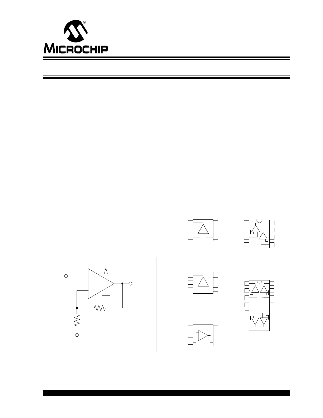
Typical Application
V
DD
V
IN
R
2
Non-Inverting Amplifier
V
REF
+
MCP6001
–
R
1
Gain 1
V
OUT
V
SS
R
1
----- -
+=
R
2
Description
The Microchip T echnology Inc. MCP6001/2/4 family of
operational amplifiers (op amps) is specifically
designed for general-purpose applications. This family
has a 1 MHz Gain Bandwidth Product (GBWP) and
90° phase margin (typ.). It also maintains 45° phase
margin (typ.) with a 500 pF capacitive load. This family
operates from a single supply voltage as low as 1.8V,
while drawing 100 µA (typ.) quiescent current.
Additionally, the MCP6001/2/4 supports rail-to-rail
input and output swing, with a common mode input
voltage range of V
+300mV to VSS– 300 mV. This
DD
family of op amps is designed with Microchip’s
advanced CMOS process.
The MCP6001/2/4 family is available in the industrial
and extended tempera ture ranges, w ith a power sup ply
range of 1.8V to 5.5V.
Package Types
MCP6001
SC-70-5, SOT-23-5
V
V
1
1
OUT
OUT
V
V
VIN+
SS
SS
+
+
2
2
3
3
-
-
MCP6001R
SOT-23-5
V
1
OUT
V
VIN+
DD
+
2
3
-
MCP6001U
SOT-23-5
VIN+
1
V
VIN–
SS
+
2
-
3
V
V
DD
DD
VIN–
V
SS
VIN–
V
DD
V
OUT
V
V
V
V
V
5
5
4
4
5
4
5
4
MCP6002
PDIP, SOIC, MSOP
V
OUTA
INA
INA
V
1
–
2
-
+
3
4
SS
8
DD
7
+
V
OUTB
6
+
-
V
–
INB
V
+
5
INB
MCP6004
PDIP, SOIC, TSSOP
V
1
OUTA
–
V
2
V
V
V
OUTB
INA
INA
V
INB
INB
-
+
3
4
DD
+V
5
-
–
6
7
14
OUTD
V
–
13
+
-
+
+
+
IND
+
V
12
IND
V
11
SS
+
10
INC
-
–
V
9
INC
V
8
OUTC
© 2005 Microchip Technology Inc. DS21733F-page 1
Page 2
MCP6001/2/4
1.0 ELECTRICAL CHARACTERISTICS
Absolute Maximum Ratings †
VDD – VSS........................................................................7.0V
All Inputs and Outputs ...................V
Difference Input Voltage ......................................|V
Output Short-Circuit Current .................................continuous
Current at Input Pins ....................................................±2 mA
Current at Output and Supply Pins ............................±30 mA
Storage Temperature........................... .... ..... .-65°C to +150°C
Maximum Junction Temperature (T
ESD Protection On All Pins (HBM;MM)...............≥ 4 kV; 200V
– 0.3V to VDD + 0.3V
SS
– VSS|
DD
)..........................+150°C
J
† Notice: S tresses above those listed under “Maximum
Ratings” may cause permanent damage to the device.
This is a stress rating only and functional operation of
the device at tho se or any oth er conditions ab ove those
indicated in the operational listings of this specification
is not implied. Exposure to maximum rating conditions
for extended periods may affect device reliability.
DC ELECTRICAL SPECIFICATIONS
Electrical Characteristics: Unless otherwise indicated, TA = +25°C, VDD = +1.8V to +5.5V, VSS = GND, VCM = VDD/2,
R
= 10 kΩ to VDD/2 and V
L
Parameters Sym Min Typ Max Units Conditions
Input Offset
Input Offset Voltage V
Input Offset Drift with Temperature ΔV
Power Supply Rejection Ratio PSRR — 86 — dB VCM = V
Input Bias Current and Impedance
Input Bias Current: I
Industrial Tempe ratu r e I
Extended Temperature I
Input Offset Current I
Common Mode Input Impedance Z
Differential Input Impedance Z
Common Mode
Common Mode Input Range V
Common Mode Rejection Ratio CMRR 60 76 — dB V
Open-Loop Gain
DC Open-Loop Gain (Large Signal) A
Output
Maximum Output Voltage Swing V
Output Short-Circuit Current I
Power Supply
Supply Voltage V
Quiescent Current per Amplifier I
Note 1: MCP6001/2/4 parts w ith date codes prior to De cemb er 2004 (week code 49) were teste d to ± 7mV minimum/
maximum limits.
OUT
≈ VDD/2.
OS
/ΔT
OS
B
B
B
OS
CM
DIFF
CMR
OL
, VOHVSS + 25 — VDD – 25 mV VDD = 5.5V
OL
SC
DD
Q
-4.5 — +4.5 mV VCM = VSS (Note 1)
—±2.0—µV/°CT
A
= -40°C to +125°C,
A
= V
V
CM
—±1.0—pA
—19—pAT
= +85°C
A
— 1100 — pA TA = +125°C
—±1.0—pA
—1013||6 — Ω||pF
—1013||3 — Ω||pF
V
− 0.3 — V
SS
88 112 — dB V
—±6—mAV
—±23—mAV
+ 0.3 V
DD
CM
V
DD
OUT
V
CM=VSS
DD
DD
1.8 — 5.5 V
50 100 170 µA IO = 0, VDD = 5.5V, VCM = 5V
SS
SS
= -0.3V to 5.3V,
= 5V
= 0.3V to VDD – 0.3V,
= 1.8V
= 5.5V
DS21733F-page 2 © 2005 Microchip Technology Inc.
Page 3

MCP6001/2/4
AC ELECTRICAL SPECIFICATIONS
Electrica l Characteristics: Unless otherwise indicated, TA = +25°C, VDD = +1.8 to 5.5V, VSS = GND, VCM = VDD/2,
≈ VDD/2, RL = 10 kΩ to VDD/2 and CL = 60 pF.
V
OUT
Parameters Sym Min Typ Max Units Conditions
AC Response
Gain Bandwidth Product GBWP — 1.0 — MHz
Phase Margin PM — 90 — ° G = +1
Slew Rate SR — 0.6 — V/µs
Noise
Input Noise Voltage E
Input Noise Voltage Density e
Input Noise Current Density i
ni
ni
ni
TEMPERATURE SPECIFICATIONS
Electrica l Characteristics: Unless otherwise indicated, VDD = +1.8V to +5.5V and VSS = GND.
Parameters Sym Min Typ Max Units Conditions
Temperature Ranges
Industrial Tempe rature Range T
Extended Temperature Range T
Operating Temperature Range T
Storage Temperature Range T
Thermal Package Resistances
Thermal Resistance, 5L-SC70
Thermal Resistance, 5L-SOT-23
Thermal Resistance, 8L-PDIP θ
Thermal Resistance, 8L-SOIC (150 mil) θ
Thermal Resistance, 8L-MSOP θ
Thermal Resistance, 14L-PDIP
Thermal Resistance, 14L-SOIC
Thermal Resistance, 14L-TSSOP
Note: The industrial temperature devices operate over this extended temperature range, but with reduced
performance. In any case, the internal Junction Temperature (T
specification of +150°C.
A
A
A
A
θ
JA
θ
JA
JA
JA
JA
θ
JA
θ
JA
θ
JA
— 6.1 — µVp-p f = 0.1Hz to 10 Hz
—28—nV/√Hz f = 1 kHz
—0.6—fA/√Hz f = 1 kHz
-40 — +85 °C
-40 — +125 °C
-40 — +125 °C Note
-65 — +150 °C
—
—
331
256
—
—
°C/W
°C/W
—85—°C/W
—163—°C/W
—206—°C/W
—
—
—
70
120
100
—
—
—
) must not exceed the Absolute Maximum
J
°C/W
°C/W
°C/W
© 2005 Microchip Technology Inc. DS21733F-page 3
Page 4
MCP6001/2/4
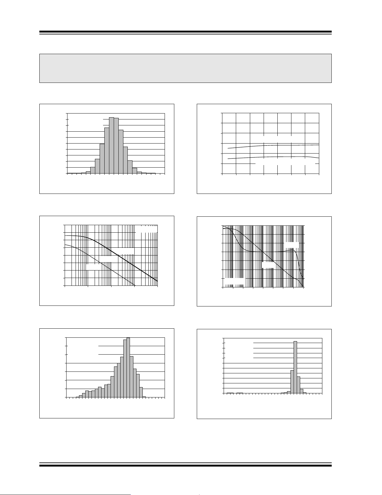
2.0 TYPICAL PERFORMANCE CURVES
Note: The graphs and t a ble s prov id ed fol low i ng thi s n ote are a statistical summary based on a l im ite d n um ber of
samples and are prov ided for informational purposes only. The performance characteristics listed herein
are not tested or guaranteed. In some graphs or tables, the data presented may be outside the specified
operating range (e.g., outside specified power supply range) and therefore outside the warranted range.
Note: Unless otherwise indicated, TA = +25°C, VDD = +1.8V to +5.5V, VSS = GND, VCM = VDD/2, V
= 10 kΩ to VDD/2 and CL = 60 pF.
R
L
OUT
≈ VDD/2,
20%
64,695 Samples
18%
V
= V
CM
SS
5
-4
-3
-2
Input Offset Voltage (mV)
0
1
2
-1
3
Percentage of Occurrences
16%
14%
12%
10%
8%
6%
4%
2%
0%
FIGURE 2-1: Input Offset Voltage.
100
90
80
70
60
50
40
PSRR, CMRR ( dB )
30
20
10 100 1k 10k 100k
1.E+01 1.E+02 1.E+03 1.E+04 1.E+05
PSRR+
CMRR
Frequency (Hz)
VCM = V
PSRR–
100
95
90
85
80
PSRR, CMRR (dB)
75
4
5
70
-50 -25 0 25 50 75 100 125
PSRR (VCM = VSS)
CMRR (VCM = -0.3V to +5.3V)
Ambient Temperature (°C)
FIGURE 2-4: CMRR, PSRR vs. Ambient Temperature.
SS
120
100
80
60
40
20
Open-Loop Gain (dB)
0
VCM = V
+00
SS
1.E
+01
-20
0.1 1 10 100 10k 100k 1M 10M
1.E-011.E
1.E
+02
1k
1.E
+03
Gain
1.E
+04
+05
Phase
1.E
1.E
+06
1.E
+07Frequency (Hz)
0
-30
-60
-90
-120
-150
-180
-210
Open-Loop Phase (°)
FIGURE 2-2: PSRR, CMRR vs. Frequency.
14%
1230 Samples
Percentage of Occurrences
12%
10%
8%
6%
4%
2%
0%
= 5.5V
V
DD
= V
V
CM
DD
TA = +85°C
0
3
6
9
12
15
18
Input Bias Current (pA)
21
24
27
30
FIGURE 2-3: Input Bias Current at +85°C.
FIGURE 2-5: Open-Loop Gain, Phase vs.
Frequency.
55%
605 Samples
50%
V
45%
40%
35%
30%
25%
20%
15%
10%
5%
Percentage of Occurrences
0%
= 5.5V
DD
= V
V
CM
DD
TA = +125°C
0
150
300
450
600
750
900
Input Bias Current (pA)
1050
1200
1350
1500
FIGURE 2-6: Input Bias Current at +125°C.
DS21733F-page 4 © 2005 Microchip Technology Inc.
Page 5
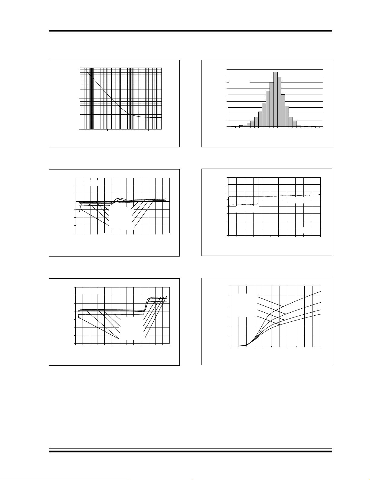
MCP6001/2/4
= -40°C
Note: Unless otherwise indicated, TA = +25°C, VDD = +1.8V to +5.5V, VSS = GND, VCM = VDD/2, V
= 10 kΩ to VDD/2 and CL = 60 pF.
R
L
1,000
Hz)
100
(nV/
Input Noise Voltage Density
10
0.1 101 100 10k1k 100k
1.E-01 1.E+001.E+011.E+021.E+031.E+041.E+0
5Frequency (Hz)
FIGURE 2-7: Input Noise Voltage Density
18%
1225 Samples
16%
14%
12%
10%
Percentage of Occurrences
8%
6%
4%
2%
0%
T
A
VCM = V
-12
= -40°C to +125°C
SS
-8-6-4
-10
Input Offset Voltage Drift (µV/°C)
0
-2
FIGURE 2-10: Input Offset Voltage Drift.
vs. Frequency.
0
VDD = 1.8V
-100
-200
-300
-400
-500
-600
Input Offset Voltage (µV)
-700
-0.4
-0.2
Common Mode Input Voltage (V)
TA = -40°C
T
= +25°C
A
T
= +85°C
A
= +125°C
T
A
0.0
0.2
0.4
0.6
0.8
1.0
1.2
1.4
1.6
1.8
2.0
2.2
200
150
100
50
0
VDD = 1.8V
0.0 0.5 1.0 1.5 2.0 2.5 3.0 3.5 4.0 4.5 5.0 5.5
Output Voltage (V)
Input Offset Voltage (µV)
-50
-100
-150
-200
≈ VDD/2,
OUT
2
4
VDD = 5.5V
6
8
VCM = V
10
12
SS
FIGURE 2-8: Input Offset Voltage vs.
Common Mode Input Voltage at V
0
VDD = 5.5V
-100
-200
-300
-400
-500
-600
Input Offset Voltage (µV)
-700
0.0
0.5
-0.5
1.0
Common Mode Input Voltage (V)
1.5
2.0
TA = -40°C
T
= +25°C
A
T
= +85°C
A
= +125°C
T
A
2.5
3.0
3.5
= 1.8V.
DD
4.0
4.5
5.0
5.5
6.0
FIGURE 2-9: Input Offset Voltage vs.
Common Mode Input Voltage at V
= 5.5V.
DD
FIGURE 2-11: Input Offset Voltage vs. Output Voltage.
30
25
T
A
TA = +25°C
20
T
= +85°C
A
T
= +125°C
A
15
10
Magnitude (mA)
Short Circuit Current
5
0
0.0 0.5 1.0 1.5 2.0 2.5 3.0 3.5 4.0 4.5 5.0 5.5
Power Supply Voltage (V)
FIGURE 2-12: Output Short-Circuit Current vs. Power Supply Voltage.
© 2005 Microchip Technology Inc. DS21733F-page 5
Page 6
MCP6001/2/4
Note: Unless otherwise indicated, TA = +25°C, VDD = +1.8V to +5.5V, VSS = GND, VCM = VDD/2, V
= 10 kΩ to VDD/2 and CL = 60 pF.
R
L
1.0
Falling Edge, VDD = 5.5V
0.9
Falling Edge, VDD = 1.8V
0.8
0.7
0.6
0.5
0.4
0.3
Slew Rate (V/µs)
0.2
Rising Edge, VDD = 5.5V
Rising Edge, VDD = 1.8V
0.1
0.0
-50 -25 0 25 50 75 100 125
Ambient Temperature (°C)
FIGURE 2-13: Slew Rate vs. Ambient Temperature.
1,000
VDD – V
100
(mV)
10
Output Voltage Headroom
1
10µ 10m1m100µ
1.E-05 1.E-04 1.E-03 1.E-02
Output Current Magnitude (A)
OH
VOL – V
SS
0.08
G = +1 V/V
0.06
0.04
0.02
0.00
-0.02
-0.04
-0.06
Output Voltage (20 mV/div)
-0.08
0.E+00 1.E-06 2.E-06 3.E-06 4.E-06 5.E-06 6. E-06 7.E-06 8.E-06 9. E-06 1.E-05
Time (1 µs/div)
FIGURE 2-16: Smal l-Signal, Non-Inverting Pulse Response.
5.0
4.5
4.0
3.5
3.0
2.5
2.0
1.5
Output Voltage (V)
1.0
0.5
0.E+00 1.E -05 2.E-05 3.E-05 4.E-05 5.E-05 6.E-05 7.E-05 8.E-05 9.E-05 1.E-04
0.0
Time (10 µs/div)
OUT
≈ VDD/2,
G = +1 V/V
V
= 5.0V
DD
FIGURE 2-14: Output Voltage Headroom vs. Output Current Magnitude.
10
)
P-P
1
Output Voltage Swing (V
0.1
1.E+03 1.E+04 1.E+05 1.E+06
VDD = 5.5V
VDD = 1.8V
1k 10k 100k 1M
Frequency (Hz)
FIGURE 2-15: Output Voltage Swing vs. Frequency.
FIGURE 2-17: Large-Signal, Non-Inverting Pulse Response.
180
VCM = VDD - 0.5V
160
140
120
100
80
60
per amplifier (µA)
40
Quiescent Current
20
TA = +125°C
T
= +85°C
A
T
= +25°C
A
= -40°C
T
A
0
0.00.51.01.52.02.53.03.54.04.55.05.5
Power Supply Voltage (V)
FIGURE 2-18: Quiescent Current vs. Power Supply Voltage.
DS21733F-page 6 © 2005 Microchip Technology Inc.
Page 7

MCP6001/2/4
3.0 PIN DESCRIPTIONS
Descriptions of the pins are listed in Table 3-1.
TABLE 3-1: PIN FUNCTION TABLE
MCP6001 MCP6001R MCP6001U MCP6002 MCP6004 Symbol Description
11411V
44322V
33133V
52584VDDPositive Power Supply
——— 5 5V
——— 6 6
——— 7 7V
————8V
————9V
————10V
252411V
————12V
————13V
————14V
OUT
IN
IN
, V
–, V
+, V
INB
V
INB
OUTB
OUTC
INC
INC
IND
IND
OUTD
SS
Analog Output (op amp A)
OUTA
– Inverting Input (op amp A)
INA
+ Non-inverting Input (op amp A)
INA
+ Non-inverting Input (op amp B)
Inverting Input (op amp B)
–
Analog Output (op amp B)
Analog Output (op amp C)
– Inverting Input (op amp C)
+ Non-inverting Input (op amp C)
Negative Power Supply
+ Non-inverting Input (op amp D)
– Inverting Input (op amp D)
Analog Output (op amp D)
3.1 Analog Outputs
The output pins are low-impedance voltage sources.
3.2 Analog Inputs
The non-inverting and inverting inputs are highimpedance CMOS inputs with low bias currents.
3.3 Power Supply (VSS and VDD)
The positive powe r s upp ly (VDD) is 1.8V to 5.5V h igh er
than the negative power supply (V
operation, the other pins are at voltages between V
and VDD.
Typically, these parts are used in a single (positive)
supply configuration. In this case, V
ground and V
is connected to the supply. VDD will
DD
need a local bypass capacitor (typically 0.01 µF to
0.1 µF) within 2 mm of the VDD pin. These parts can
share a bulk capacitor with analog parts (typically
2.2 µF to 10 µF) within 100 mm of the VDD pin.
). For normal
SS
is connected to
SS
SS
© 2005 Microchip Technology Inc. DS21733F-page 7
Page 8

MCP6001/2/4
4.0 APPLICATION INFORMATION
The MCP6001/2/4 family of op amps is manufactured
using Microchip’s state-of-the-art CMOS process and
is specifically designed for low-cost, low-power and
general-purpose applications. The low supply voltage,
low quiescent current and wide bandwidth makes the
MCP6001/2/4 ideal for battery-powered applications.
This device has high phase margin, which makes it
stable for larger capacitive load applications.
4.1 Rail-to-Rail Input
The MCP6001/2/4 op amps are designed to prev ent
phase reversal when the input pins exceed the supply
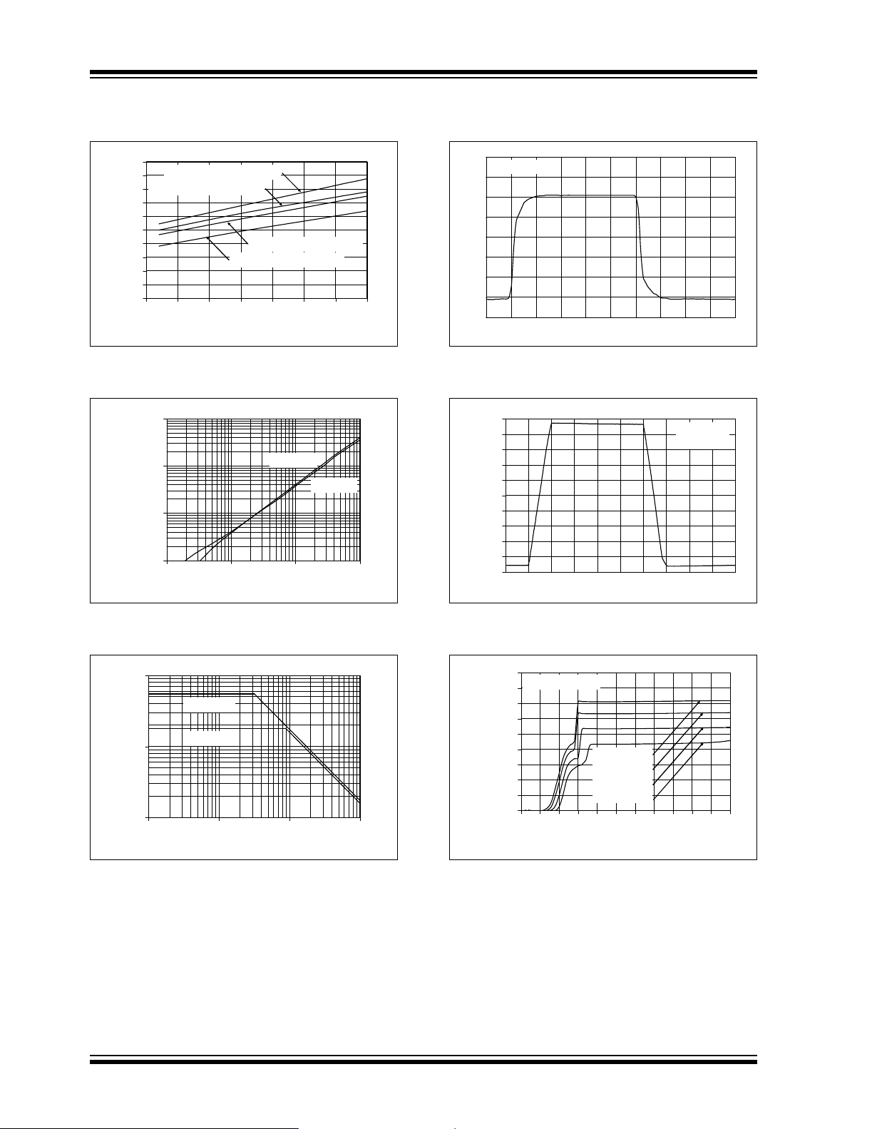
voltages. Fi gure 4-1 shows the input voltage exceeding
the supply voltage without any phase reversal.
6
5
4
3
2
1
0
Input, Output Voltages (V)
0.E+00 1.E-05 2.E-0 5 3.E-05 4.E-05 5.E-05 6.E-05 7. E-05 8.E-05 9.E-05 1.E-04
-1
V
V
OUT
Time (10 µs/div)
IN
FIGURE 4-1: The MCP6001/2/4 Show No Phase Reversal.
The input stage of the MCP6001/2/4 op amps use two
differential input stages in parallel. One operates at a
low common mode inp ut vol t age (V
operates at a high V
operates with a V
300 mV below V
measured at V
CM=VSS
to ensure proper operation.
Input voltages that exceed the input voltage range
– 0.3V to VDD+ 0.3V at 25°C) can cause
(V
SS
excessive current to flow i nto or out of the input pins ,
while current beyond ±2mA can cause reliability
problems. Applications tha t exceed thi s rating mu st be
externally limited with a resistor, as shown in Figure 4-2.
. With this topology, the device
CM
up to 300 mV above VDD and
CM
. The input offset voltage is
SS
– 300 mV and VDD+300mV
VDD = 5.0V
G = +2 V/V
), while the other
CM
–
IN
V
OUT
R
IN
V
IN
Maximum expected V
()VDD–
-------------------------------------------------------------------------------
R
≥
IN
V
SS
----------------------------------------------------------------------------
R
≥
IN
MCP600X
+
IN
2 mA
Minimum expected V
()–
2 mA
FIGURE 4-2: Input Current Limiting
Resistor (R
IN
).
4.2 Rail-to-Rail Output
The output volt age rang e of the MCP6001 /2/4 op a mps
–25mV (min.) and VSS + 25 mV (max.) when
is V
DD
=10kΩ is connected to VDD/2 and VDD = 5.5V.
R
L
Refer to Figure 2-14 for more information.
4.3 Capacitive Loads
Driving large capacitive loads can cause stability problems for volt age f eedbac k op amp s. As the load cap acitance increases, the feedback loop’s phase margin
decreases and the closed-loop bandwidth is reduced.
This produces gain pe aking in th e frequency response,
with overshoot and ringing in the step response. While
a unity-gain buffer (G = +1) is the most sensitive to
capacitive loads, all gains show the same general
behavior.
When driving large capacitive loads with these op
amps (e.g., > 100 pF when G = +1), a small series
resistor at the output (R
feedback loop’s phase margin (stability) by making the
output load resistive at higher frequencies. The bandwidth will b e generally lower than the bandwid th with n o
capacitance load.
–
MCP600X
V
IN
+
in Figure 4-3) improves the
ISO
R
ISO
C
L
V
OUT
FIGURE 4-3: Output resistor, R
ISO
stabiliz es large capacitive loads.
DS21733F-page 8 © 2005 Microchip Technology Inc.
Page 9
MCP6001/2/4
:
:
Figure 4-4 gives recommended R
values for
ISO
different capacitive loads and gains. The x-axis is the
normalized lo ad ca paci tan c e (CL/GN), where GN is the
L/GN
ISO
and the
N
10n
(F)
values
is
N
circuit's noise gain. For non-inverti ng gains, G
Signal Gain are equal. For inverting gains, G
1+|Signal Gain| (e.g., -1 V/V gives G
1000
)
(
Recommended R
VDD = 5.0V
R
= 100 k
L
ISO
100
GN = 1
t 2
G
N
10
10p
1.E-11 1.E-10 1.E-09 1.E-08
Normalized Load Capacitance; C
100p 1n 10n
= +2 V/V).
N
FIGURE 4-4: Recommended R
for Capacitive Loads.
After sele cting R
resulting frequency response peaking and step
response overshoot. Modify R
response is reasonable. Bench evaluation and simulations with the MCP6001/2/4 SPICE macro model are
very helpful.
for your circuit, double-check the
ISO
’s value until the
ISO
4.4 Supply Bypass
With this family of operational amplifiers, the power
supply pin (V
bypass capacitor (i.e., 0.01 µF to 0.1 µF) within 2 mm
for good high-frequency performance. It also needs a
bulk capacito r (i.e., 1 µF or la rger) within 100 mm to
provide large, s low current s. This bulk c apac itor can b e
shared with other analog parts.
for single-supply) should have a local
DD
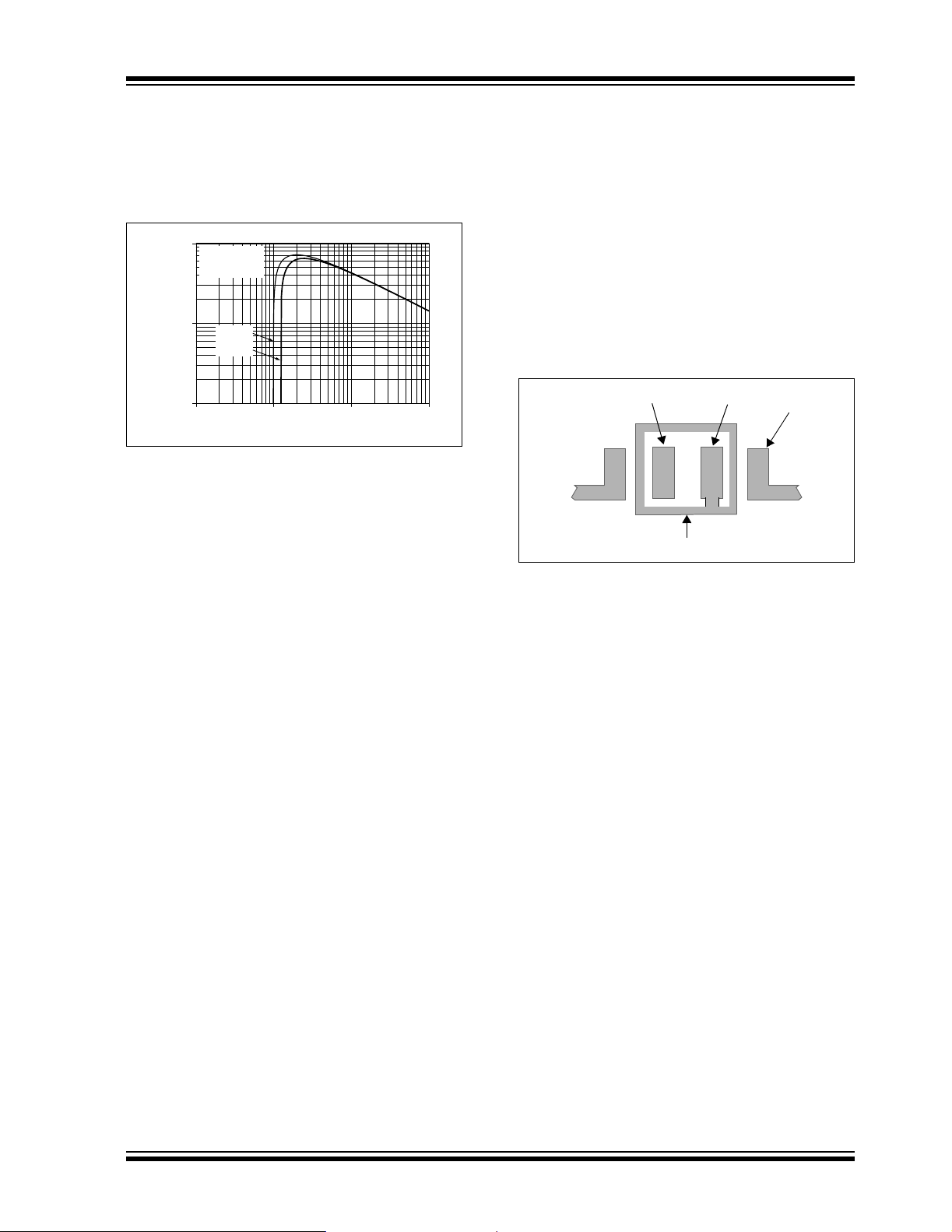
4.5 PCB Surface Leakage
In applications where low input bias current is critical,
Printed Circuit Board (PCB) surface leakage effects
need to be considered. Surface leakage is caused by
humidity, dust or other contamination on the board.
Under low humidity conditions, a typical resistance
between nearby traces is 1 0
cause 5 pA of current to flow; which is greater than the
MCP6001/2/4 family’ s bias c urrent at 25°C (1 pA, typ.).
The easiest way to reduce surface leakage is to use a
guard ring around se nsi tiv e p ins (or t race s). The gua rd
ring is biased at the same voltage as the sensitive pin.
An example of this type of layout is shown in
Figure 4-5.
VIN-V
FIGURE 4-5: Example Guard Ring Layout for Inverting Gain.
1. Non-inverting Gain and Unity-Gain Buffer:
a. Connect the non-inverting pin (V
input with a wire that does not touch the
PCB surface.
b. Connect the guard ring to the inverting input
pin (V
common mode input voltage.
2. Inverting Gain and Transimpedance Gain
Amplifiers (convert current to voltage, such as
photo detectors):
a. Connect the guard ring to the non-inverting
input pin (V
to the same reference voltage as the op
amp (e.g., V
b. Connect the inverting pin (VIN–) to the input
with a wire that does not touch the PCB
surface.
–). This biases the g uard rin g t o th e
IN
12
Ω. A 5V dif ference would
+
IN
V
SS
Guard Ring
+) to the
IN
+). This bi ases the gua rd ri ng
IN
/2 or ground).
DD
© 2005 Microchip Technology Inc. DS21733F-page 9
Page 10

MCP6001/2/4
4.6 Application Circuits
4.6.1 UNITY-GAIN BUFFER
The rail-to-rail input and output capability of the
MCP6001/2/4 op amp is ideal for unity-gain buffer
applications. The low quiescent current and wide
bandwidth makes the device suitable for a buffer
configuration in an instrumentation amplifier circuit, as
shown in Figure 4-6.
–
1/2
V
OUT
MCP6002
+
–
1/2
MCP6002
+
V
IN1
V
IN2
R
2
R
2
V
–()
IN2VIN1
FIGURE 4-6: Instrumentation Amplifier with Unit y-Gain Buffer Inputs.
4.6.2 ACTIVE LOW-PASS FILTER
The MCP6001/2/4 op amp’s low input bias current
makes it possible for the designer to use larger resistors and smaller capacitors for active low-pass filter
applications. Howev er , as the res istance increases, th e
noise generated also in creases. Parasitic capacitan ces
and the large value resistors could also modi fy the frequency response. These trade-offs need to be
considered when selecting circuit elements.
Usually, the op amp bandwidth is 100X the filter cutoff
frequency (or higher) for good perf or mance. It is p ossible to have the op amp bandwidth 10X higher th an the
cutoff frequency, thus having a design that is more
sensitive to component tolerances.
Figure 4-7 shows a second-order Butterworth filter with
100 kHz cutoff frequency and a gain of +1 V/V; the op
amp bandwidth is only 10X higher than the cutoff
frequency. The component values were sel ecte d usin g
Microchip’s FilterLab
®
software.
R
1
–
MCP6001
+
R
1
V
REF
R
1
------
+=
• V
R
2
V
OUT
R1 = 20 kΩ
= 10 kΩ
R
2
REF
100 pF
V
IN
14.3 kΩ
53.6 kΩ
33 pF
+
MCP6002
–
V
OUT
FIGURE 4-7: Active Second-Order Low- Pass Filter.
4.6.3 PEAK DETECTOR
The MCP6001/2/4 op amp ha s a high input impeda nce,
rail-to-rail input/outp ut and low input bias current , which
makes this device suitable for peak detector applications. Figure 4-8 shows a peak detector circuit with
clear and sample switches. The peak-detection cycle
uses a clock (CLK), as shown in Figure4-8.
At the rising edge of CLK, Sample Switch closes to
SAMP
is sam-
1
. A t t h e
begin sampling. The peak volt age stored on C
pled to C
for a sample time defined by t
2
end of the sampl e time (f all ing edge of Sample Sig nal),
Clear Signal goes high and closes the Clear Switch.
When the Clear Switch closes, C
R
for a time defined by t
1
CLEAR
discharges through
1
. At the end of the clear
time (falling edge of Clear Signal), op amp A begins to
store the peak value of V
t
In order to define t
DETECT
.
SAMP
on C1 for a time defined by
IN
and t
, it is necessary to
CLEAR
determine the capacitor charging and discharging
period. The capacitor charging ti me is limited by the
amplifier source current, while the discharging time (
is defined using R
(τ = R1C1). t
1
the input signal is sampled on C
is the time that
DETECT
and is dependent on
1
τ)
the input voltage change frequency.
The op amp output current limit, and the size of the
storage capacitors (both C
ing limitations as the input voltage (V
and C2), could create slew-
1
) increases.
IN
Current through a capacitor is dep endent on the size of
the capacitor and the rate of volt age ch ange. From this
relationship, the rate of vol tage ch ange or the sle w rate
can be determined. For exam ple, with an op amp shortcircuit current of I
= 0.1 µF, then:
C
1
= 25 mA and a load capaci tor of
SC
EQUATION 4-1:
dV
C1
=
=
=
250mV μs⁄=
C
1
I
SC
------- -
C
1
25mA
-------------- -
0.1μF
-------------
dt
dV
-------------
dV
C1
-------------
dt
dt
C1
I
SC
DS21733F-page 10 © 2005 Microchip Technology Inc.
Page 11

This voltage rate of change is less than the MCP6001/2/4
slew rate of 0.6 V/µs. When the input voltage swings
below the voltage across C1, D1 becomes reversebiased. This opens the feedback loop and rails the
amplifier. When the input voltage increases, the amplifier
recovers at its slew rate. Based on the rate of voltage
change shown in the above equation, it takes an
extended period of time to charge a 0.1 µF capacitor. The
capacitors need to be selected so that the circuit is not
limited by the amplifier slew rate. Therefore, the capacitors should be less than 40 µF and a stabilizing resistor
) needs to be properly selected. (Refer to
(R
ISO
Section 4.3 “Capacitive Loads”).
V
IN
+
1/2
D
R
1
ISO
V
C1
MCP6002
–
Op Amp A
C
R
1
1
+
1/2
MCP6002
–
Op Amp B
MCP6001/2/4
R
V
ISO
C2
+
MCP6001
C
2
–
Op Amp C
V
OUT
Sample
Switch
Clear
Switch
t
SAMP
Sample Signal
t
CLEAR
Clear Signal
t
DETECT
CLK
FIGURE 4-8: Peak Detector with Clear and Sample CMOS Analog Switches.
© 2005 Microchip Technology Inc. DS21733F-page 11
Page 12

MCP6001/2/4
5.0 DESIGN TOOLS
Microchip provides the basic design tools needed for
the MCP6001/2/4 family of op amps.
5.1 SPICE Macro Model
The latest SPICE macro model for the MCP6001/2/4
op amps is available on our web site at
www.microchip.com. This model is intended to be an
initial design tool that works well in the op amp’s linear
region of operation at room temperature. See the
model file for information on its capabilities.
Bench testing is a very im portant par t of any design an d
cannot be replaced with simulations. Also, simulation
results using th is ma cro m od el ne ed to be v ali dated by
comparing them to the data sheet spec ifications and
characteristic curves.
5.2 FilterLab® Software
Microchip’s FilterLab® software is an innovative
software tool that simplifies analog active filter (using
op amps) design. A vailable at no cost fr om our web site
at www.microchip.com, the FilterLab design tool
provides full schematic di agrams of the filter circuit with
component values. It also outputs the filter circuit in
SPICE format, which can be used with the macro
model to simulate actual filter performance.
DS21733F-page 12 © 2005 Microchip Technology Inc.
Page 13

6.0 PACKAGING INFORMATION
6.1 Package Marking Information
MCP6001/2/4
5-Lead SC-70 (MCP6001)
XXN (Front)
Device
YWW (Back)
MCP6001 AAN CDN
Note: Applies to 5-Lead SC-70.
OR
XXNN
5-Lead SOT-23 (MCP6001/1R/1U)
5
4
XXNN
1 23
Device
MCP6001 AANN CDNN
Note: Applies to 5-Lead SC-70.
Device
MCP6001 AANN CDNN
MCP6001R ADNN CENN
MCP6001U AFNN CFNN
Note: Applies to 5-Lead SOT-23.
I-Temp
Code
I-Temp
Code
I-Temp
Code
E-Temp
Code
E-Temp
Code
E-Temp
Code
Example: (I-Temp)
AA7 (Front)
432 (Back)
OR
AA74
Example: (E-Temp)
5
4
CD25
1 23
8-Lead PDIP (300 mil)
XXXXXXXX
XXXXXNNN
YYWW
Example:
MCP6002
I/P256
0432
Legend: XX...X Customer specific information*
YY Year code (last 2 digits of calendar year)
WW Week code (week of January 1 is week ‘01’)
NNN Alphanumeric traceability code
Note: In the event the full Micro chip p art num ber can not be ma rked on on e line, it will
be carried over to the next line thus limiti ng the number of available characters
for customer specific information.
* Standard marking consists of Microchip part number, year code, week code, traceability code (facility
code, mask rev#, and assembly code). For marking beyond this, certain price adders apply. Please
check with your Microchip Sales Office.
© 2005 Microchip Technology Inc. DS21733F-page 13
Page 14

MCP6001/2/4
Package Marking Information (Continued)
8-Lead SOIC (150 mil)
XXXXXXXX
XXXXYYWW
NNN
8-Lead MSOP
XXXXXX
YWWNNN
14-Lead PDIP (300 mil) (MCP6004)Example:
XXXXXXXXXXXXXX
XXXXXXXXXXXXXX
YYWWNNN
Example:
MCP6002
I/SN0432
256
Example:
6002I
432256
MCP6004-I/P
0432256
14-Lead SOIC (150 mil) (MCP6004)
XXXXXXXXXX
XXXXXXXXXX
YYWWNNN
14-Lead TSSOP (MCP6004)
XXXXXX
YYWW
NNN
Example:
MCP6004ISL
0432256
Example:
6004ST
0432
256
DS21733F-page 14 © 2005 Microchip Technology Inc.
Page 15

5-Lead Plastic Package (SC-70)
E
E1
MCP6001/2/4
D
p
n
Q1
c
Number of Pins
Pitch
Molded Package Thickness
Standoff
Molded Package Width
Top of Molded Pkg to Lead Shoulder
Lead Thickness
A2
A1
E1
Q1
B
1
A2
A1
L
MILLIMETERS*INCHESUnits
MINDimension Limits
n
p
c
NOM
.004 .016 0.10 0.40
MINMAX
NOM
55
0.65 (BSC).026 (BSC)
A
MAX
1.100.80.043.031AOverall Height
1.000.80.039.031
0.100.00.004.000
2.401.80.094.071EOverall Width
1.351.15.053.045
2.201.80.087.071DOverall Length
0.300.10.012.004LFoot Length
0.180.10.007.004
0.300.15.012.006BLead Width
*Controlling Parameter
Notes:
Dimensions D and E1 do not include mold flash or protrusions. Mold flash or protrusions shall not
exceed .005" (0.127mm) per side.
JEITA (EIAJ) Standard: SC-70
Drawing No. C04-061
© 2005 Microchip Technology Inc. DS21733F-page 15
Page 16

MCP6001/2/4
5-Lead Plastic Small Outline Transistor (OT) (SOT23)
E
E1
p
B
p1
D
n
c
β
Number of Pins
Pitch
Outside lead pitch (basic)
Foot Angle
Lead Thickne ss
Mold Draft Angle Top
Mold Draft Angle Bottom
* Controlling Parameter
§ Significant Characteristic
Notes:
Dimensions D and E1 do not include mold flash or protrusions. Mold flash or protrusions shall not exceed
.010” (0.254mm) per side.
JEDEC Equivalent: MO-178
Drawing No. C04-091
1
A
φ
L
n
p
p1
φ
c
α
β
.038
A1
MILLIMETERSINCHES*Units
0.95
1.90.075
α
A2
MAXNOMMINMAXNOMMINDimension Limits
55
1.451.180.90.057.046.035AOverall Height
1.301.100.90.051.043.035A2Molded Packag e Thick ness
0.150.080.00.006.003.000A1Standoff §
3.002.802.60.118.110.102EOverall Width
1.751.631.50.069.064.059E1Molded Package Width
3.102.952.80.122.116.110DOverall Length
0.550.450.35.022.018.014LFoot Length
10501050
0.200.150.09.008.006.004
0.500.430.35.020.017.014BLead Width
10501050
10501050
DS21733F-page 16 © 2005 Microchip Technology Inc.
Page 17

8-Lead Plastic Dual In-line (P) – 300 mil (PDIP)
E1
D
2
MCP6001/2/4
n
E
β
eB
Number of Pins
Pitch
Top to Seating Plane A .140 .155 .170 3.56 3.94 4.32
Molded Package Thickness A2 .115 .130 .145 2.92 3.30 3.68
Base to Seating Plane A1 .015 0.38
Shoulder to Shoulder Width E .300 .313 .325 7.62 7.94 8.26
Molded Package Width E1 .240 .250 .260 6.10 6.35 6.60
Overall Length D .360 .373 .385 9.14 9.46 9.78
Tip to Seating Plane L .125 .130 .135 3.18 3.30 3.43
Lead Thickness
Upper Lead Width B1 .045 .058 .070 1.14 1.46 1.78
Lower Lead Width B .014 .018 .022 0.36 0.46 0.56
Overall Row Spacing § eB .310 .370 .430 7.87 9.40 10.92
Mold Draft Angle Top
Mold Draft Angle Bottom
* Controlling Parameter
§ Significant Characteristic
Notes:
Dimensions D and E1 do not include mold flash or protrusions. Mold flash or protrusions shall not exceed
.010” (0.254mm) per side.
JEDEC Equivalent: MS-001
Drawing No. C04-018
Dimension Limits MIN NOM MAX MIN NOM MAX
1
α
A
c
Units INCHES* MILLIMETERS
n
p
c
α
β
.008 .012 .015 0.20 0.29 0.38
A1
B1
B
88
.100 2.54
51015 51015
51015 51015
A2
L
p
© 2005 Microchip Technology Inc. DS21733F-page 17
Page 18

MCP6001/2/4
8-Lead Plastic Small Outline (SN) – Narrow, 150 mil (SOIC)
E
E1
p
D
2
B
Number of Pins
Pitch
Foot Angle
Lead Thickness
Mold Draft Angle Top
Mold Draft Angle Bottom
* Controlling Parameter
§ Significant Characteristic
Notes:
Dimensions D and E1 do not include mold flash or protrusions. Mold flash or protrusions shall not exceed
.010” (0.254mm) per side.
JEDEC Equivalent: MS-012
Drawing No. C04-057
n
45°
c
β
n
p
φ
c
α
β
1
h
A
φ
L
048048
A1
MILLIMETERSINCHES*Units
1.27.050
α
A2
MAXNOMMINMAXNOMMINDimension Limits
88
1.751.551.35.069.061.053AOverall Height
1.551.421.32.061.056.052A2Molded Package Thickness
0.250.180.10.010.007.004A1Standoff §
6.206.025.79.244.237.228EOverall Width
3.993.913.71.157.154.146E1Molded Package Width
5.004.904.80.197.193.189DOverall Length
0.510.380.25.020.015.010hChamfer Distance
0.760.620.48.030.025.019LFoot Length
0.250.230.20.010.009.008
0.510.420.33.020.017.013BLead Width
1512015120
1512015120
DS21733F-page 18 © 2005 Microchip Technology Inc.
Page 19

8-Lead Plastic Micro Small Outline Package (MS) (MSOP)
E
E1
p
D
2
B
n 1
MCP6001/2/4
α
L
8
.033
.006
.012
A
φ
A1
MAX NOM
--
.043
.037
.006
-
.009
.016
-
MIN
.031
15°
15°
0.75
0.00
0.40
0.08
0.22
c
(F)
β
Dimension Limits
Units
Number of Pins
Pitch
Overall Height
Molded Package Thickness
Standoff
Overall Width
Molded Package Width
Overall Length
Foot Length
Foot Angle
Lead Thickness
Lead Width
Mold Draft Angle Top
Mold Draft Angle Bottom
*Controlling Parameter
Notes:
Dimensions D and E1 do not include mold flash or protrusions. Mold flash or protrusions shall not
exceed .010" (0.254mm) per side.
JEDEC Equivalent: MO-187
Drawing No. C04-111
MIN
n
p
A
A2
A1
E
E1
D
L
φ
c
B
α
β
INCHES
NOM
.026 BSC
.030
.000
.193 TYP.
.118 BSC
.118 BSC
.016 .024
.037 REFFFootprint (Reference)
0° - 8°
.003
.009
5°
5° -
MILLIMETERS*
8
0.65 BSC
--
0.85
4.90 BSC
3.00 BSC
3.00 BSC
0.60
0.95 REF
0°
MAX
-
-
-
-
A2
1.10
0.95
0.15
0.80
8°
0.23
0.40
15°5° 15°5° -
© 2005 Microchip Technology Inc. DS21733F-page 19
Page 20

MCP6001/2/4
14-Lead Plastic Dual In-line (P) – 300 mil (PDIP)
E1
D
2
n
E
β
eB
Number of Pins
Pitch
Top to Seating Plane A .140 .155 .170 3.56 3.94 4.32
Molded Package Thickness A2 .115 .130 .145 2.92 3.30 3.68
Base to Seating Plane A1 .015 0.38
Shoulder to Shoulder W idth E .300 .313 .325 7.62 7.94 8.26
Molded Package Width
Overall Length D .740 .750 .760 18.80 19.05 19.30
Tip to Seating Plane L .125 .130 .135 3.18 3.30 3.43
Lead Thickness
Upper Lead Width B1 .045 .058 .070 1.14 1.46 1.78
Lower Lead Width B .014 .018 .022 0.36 0.46 0.56
Overall Row Spacing § eB .310 .370 .430 7.87 9.40 10.92
Mold Draft Angle Top
Mold Draft Angle Bottom
* Controlling Parameter
§ Significant Characteristic
Notes:
Dimensions D and E1 do not include mold flash or protrusions. Mold flash or protrusions shall not exceed
.010” (0.254mm) per side.
JEDEC Equivalent: MS-001
Drawing No. C04-005
1
A
c
A1
Dimension Limits MIN NOM MAX MIN NOM MA X
Units INCHES* MILLIMETERS
n
p
E1
c
α
β
.240 .250 .260 6.10 6.35 6.60
.008 .012 .015 0.20 0.29 0.38
5 10 15 5 10 15
5 10 15 5 10 15
B1
B
14 14
.100 2.54
α
A2
L
p
DS21733F-page 20 © 2005 Microchip Technology Inc.
Page 21

14-Lead Plastic Small Outline (SL) – Narrow, 150 mil (SOIC)
E
E1
p
D
2
B
n
1
MCP6001/2/4
45°
c
β
Number of Pins
Pitch
Foot Angle
Lead Thickne ss
Mold Draft Angle Top
Mold Draft Angle Bottom
* Controlling Parameter
§ Significant Characteristic
Notes:
Dimensions D and E1 do not include mold flash or protrusions. Mold flash or protrusions shall not exceed
.010” (0.254mm) per side.
JEDEC Equivalent: MS-012
Drawing No. C04-065
h
A
φ
L
n
p
φ
c
α
β
A1
048048
α
MILLIMETERSINCHES*Units
A2
MAXNOMMINMAXNOMMINDimension Limits
1414
1.27.050
1.751.551.35.069.061.053AOverall Height
1.551.421.32.061.056.052A2Molded Package Thickness
0.250.180.10.010.007.004A1Standoff §
6.205.995.79.244.236.228EOverall Width
3.993.903.81.157.154.150E1Molded Package Width
8.818.698.56.347.342.337DOverall Length
0.510.380.25.020.015.010hChamfer Distance
1.270.840.41.050.033.016LFoot Length
0.250.230.20.010.009.008
0.510.420.36.020.017.014BLead Width
1512015120
1512015120
© 2005 Microchip Technology Inc. DS21733F-page 21
Page 22

MCP6001/2/4
14-Lead Plastic Thin Shrink Small Outline (ST) – 4.4 mm (TSSOP)
E
E1
p
D
2
n
B
1
A
c
φ
β
Number of Pins
Pitch
Foot Angle
Lead Thickne ss
Mold Draft Angle Top
Mold Draft Angle Bottom
* Controlling Parameter
§ Significant Characteristic
Notes:
Dimensions D and E1 do not include mold flash or protrusions. Mold flash or protrusions shall not exceed
.005” (0.127mm) per side.
JEDEC Equivalent: MO-153
Drawing No. C04-087
n
p
φ
c
α
β
L
MILLIMETERS*INCHESUnits
0.65.026
α
A2A1
MAXNOMMINMAXNOMMINDimension Limits
1414
1.10.043AOverall Height
0.950.900.85.037.035.033A2Molded Package Thickness
0.150.100.05.006.004.002A1Standoff §
6.506.386.25.256.251.246EOverall Width
4.504.404.30.177.173.169E1Molded Pa ckag e Width
5.105.004.90.201.197.193DMolded Package Length
0.700.600.50.028.024.020LFoot Length
840840
0.200.150.09.008.006.004
0.300.250.19.012.010.007B1Lead Width
10501050
10501050
DS21733F-page 22 © 2005 Microchip Technology Inc.
Page 23

APPENDIX A: REVISION HISTORY
Revision F (March 2005)
Updated 6.0 “Packaging Information” to include old
and new packaging examples.
Revision E (December 2004)
The following is the list of modifications:
1. V
2. Corrected package markings in Section 6.0
3. Added Appendix A: Revision History.
Revision D (May 2003)
Revision C (December 2002)
Revision B (October 2002)
specification reduced to ±4.5 mV from
OS
±7.0 mV for parts starting with date code
YYWW = 0449
“Packaging Information”
MCP6001/2/4
Revision A (June 2002)
Original data sheet release.
© 2005 Microchip Technology Inc. DS21733E-page 23
Page 24

MCP6001/2/4
NOTES:
DS21733E-page 24 © 2005 Microchip Technology Inc.
Page 25

MCP6001/2/4
PRODUCT IDENTIFICATION SYSTEM
To order or obtain information, e.g., on pricing or delivery, refer to the factory or the listed sales office.
PART NO. X /XX
Device
PackageTemperature
Range
Device: MCP6001T: Single Op Amp (Tape and Reel)
MCP6001RT: Single Op Amp (Tape and Reel) (SOT-23)
MCP6001UT: Single Op Amp (Tape and Reel) (SOT-23)
MCP6002: Dual Op Amp
MCP6002T: Dual Op Amp (Tape and Reel)
MCP6004: Quad Op Amp
MCP6004T: Quad Op Amp (Tape and Reel)
Temperature Range: I = -40°C to +85°C
Package: LT = Plastic Package (SC-70), 5-lead (MCP6001 only)
E = -40°C to +125°C
OT = Plastic Small Outline Transistor (SOT-23), 5-lead
MS = Plastic MSOP, 8-lead
P = Plastic DIP (300 mil Body), 8-lead, 14-lead
SN = Plastic SOIC, (150 mil Body), 8-lead
SL = Plastic SOIC (150 mil Body), 14-lead
ST = Plastic TSSOP (4.4mm Body), 14-lead
(SC-70, SOT-23)
(SOIC, MSOP)
(SOIC, MSOP)
(MCP6001, MCP6001R, MCP6001U)
Examples:
a) MCP6001T-I/LT: Tape and Reel,
Industrial Temperature,
5LD SC-70 package
b) MCP6001T-I/OT: Tape and Reel,
Industrial Temperature,
5LD SOT-23 package.
c) MCP6001RT-I/OT: Tape and Reel,
Industrial Temperature,
5LD SOT-23 package.
d) MCP6001UT-E/OT: Tape and Reel,
Extended Temperature,
5LD SOT-23 package.
a) MCP6002-I/MS: Industrial Temperature,
8LD MSOP package.
b) MCP6002-I/P: Industrial Temperature,
8LD PDIP package.
c) MCP6002-E/P: Extended Temperat ure,
8LD PDIP package.
d) MCP6002-I/SN: Industrial Temperature,
8LD SOIC package.
e) MCP6002T-I/MS: Tape and Reel,
Industrial Temperature,
8LD MSOP package.
a) MCP6004-I/P: Industrial Temperature,
14LD PDIP package.
b) MCP6004-I/SL: Industrial T emperature,,
14LD SOIC package.
c) MCP6004-E/SL: Extended T emperature,,
14LD SOIC package.
d) MCP6004-I/ST: Industrial Temperature,
14LD TSSOP package.
e) MCP6004T-I/SL: Tape and Reel,
Industrial Temperature,
14LD SOIC package.
f) MCP6004T-I/ST: Tape and Reel,
Industrial Temperature,
14LD TSSOP package.
Sales and Support
Data Sheets
Products supported by a preliminary Data Sheet may have an errata sheet describing minor operational differences and
recommended workarounds. To determine if an errata sheet exists for a particular device, please contact one of the following:
1. Your local Microchip sales off ice
2. The Microchip Worldwide Site (www.microchip.com)
Please specify which device, revision of silicon and Data Sheet (include Literature #) you are using.
Customer Notification System
Register on our web site (www.microchip.com) to receive the most current information on our products.
© 2005 Microchip Technology Inc. DS21733E-page 25
Page 26

MCP6001/2/4
NOTES:
DS21733E-page 26 © 2005 Microchip Technology Inc.
Page 27

Note the following details of the code protection feature on Microchip devices:
• Microchip products meet the specification contained in their particular Microchip Data Sheet.
• Microchip believes that its family of products is one of the most secure families of its kind on t he market today, when used i n the
intended manner and under normal conditions.
• There are dishonest and possibly illegal methods used to breach the code protection feature. All of these methods, to our
knowledge, require using the Microchip products in a manner outside the operating specifications contained in Microchip’s Data
Sheets. Most likely, the person doing so is engaged in theft of intellectual property.
• Microchip is willing to work with the customer who is concerned about the integrity of their code.
• Neither Microchip nor any other semiconductor manufacturer can guarantee the security of their code. Code protection does not
mean that we are guaranteeing the product as “unbreakable.”
Code protection is constantly evolving. We at Microchip are com mitted to continuously improving the code protect ion f eatures of our
products. Attempts to break Microchip’s code protection feature may be a violation of the Digit al Mill ennium Copyright Act. If such acts
allow unauthorized access to your software or other copyrighted work, you may have a right to sue for relief under that Act.
Information contained in this publication regarding device
applications and the like is provided only for your convenience
and may be superseded by updates. It is your responsibility to
ensure that your application meets with your specifications.
MICROCHIP MAKES NO REPRESENTATIONS OR WARRANTIES OF ANY KIND WHETHER EXPRESS OR IMPLIED,
WRITTEN OR ORAL, STATUTORY OR OTHERWISE,
RELATED TO THE INFORMATION, INCLUDING BUT NOT
LIMITED TO ITS CONDITION, QUALITY, PERFORMANCE,
MERCHANTABILITY OR FITNESS FOR PURPOSE.
Microchip disclaims all liability arising from this information and
its use. Use of M icrochip’s prod ucts as critical components in
life support systems is not authorized except with express
written approval by Microchip. No licenses are conveyed,
implicitly or otherwise, under any Microchip intellectual property
rights.
Trademarks
The Microchip name and logo, the Microchip logo, Accuron,
dsPIC, K
EELOQ, microID, MPLAB, PIC, PICmicro,
PICSTART, PRO MATE, PowerSmart, rfPIC, and
SmartShunt are registered trademarks of Microchip
Technology Incorporated in the U.S.A. and other countries.
AmpLab, FilterLab, MXDEV, MXLAB, PICMASTER, SEEVAL,
SmartSensor and The Embedded Control Solutions Company
are registered trademarks of Microchip Technology
Incorporated in the U.S.A.
Analog-for-the-Digital Age, Application Maestro, dsPICDEM,
dsPICDEM.net, dsPICworks, ECAN, ECONOMONITOR,
FanSense, FlexROM, fuzzyLAB, In-Circuit Serial
Programming, ICSP, ICEPI C, Migra table Memory, MPASM,
MPLIB, MPLINK, MPSIM, PICkit, PICDEM, PICDEM.net,
PICLAB, PICtail, PowerCal, PowerInfo, PowerMate,
PowerTool, rfLAB , rfPICD EM, Select Mode, Sm art Serial,
SmartTel and Total Endurance are trademarks of Microchip
Technology Incorporated in the U.S.A. and other countries.
SQTP is a service mark of Microchip T echnology Incorporated
in the U.S.A.
All other trademarks mentioned herein are property of their
respective companies.
© 2005, Microchip Technology Incorporated, Printed in the
U.S.A., All Rights Reserved.
Printed on recycled paper.
Microchip received ISO/TS-16949:2002 quality system certification for
its worldwide headquarters, design and wafer fabrication facilities in
Chandler and Tempe, Arizona and Mountain View, California in
October 2003. The Company’s quality system processes and
procedures are for its PICmicro
devices, Serial EEPROMs, microperipherals, nonvolatile memory and
analog products. In addition, Microchip’s quality system for the design
and manufacture of development systems is ISO 9001:2000 certified.
®
8-bit MCUs, KEELOQ
®
code hopping
© 2005 Microchip Technology Inc. DS21733E-page 27
Page 28

WORLDWIDE SALES AND SERVICE
AMERICAS
Corporate Office
2355 West Chandler Blvd.
Chandler, AZ 85224-6199
Tel: 480-792-7200
Fax: 480-792-7277
Technic al Support:
http://support.microchip.com
Web Address:
www.microchip.com
Atlanta
Alpharetta, GA
Tel: 770-640-0034
Fax: 770-640-0307
Boston
Westford, MA
Tel: 978-692-3848
Fax: 978-692-3821
Chicago
Itasca, IL
Tel: 630-285-0071
Fax: 630-285-0075
Dallas
Addison, TX
Tel: 972-818-7423
Fax: 972-818-2924
Detroit
Farmington Hills, MI
Tel: 248-538-2250
Fax: 248-538-2260
Kokomo
Kokomo, IN
Tel: 765-864-8360
Fax: 765-864-8387
Los Angeles
Mission Viejo, CA
Tel: 949-462-9523
Fax: 949-462-9608
San Jose
Mountain View, CA
Tel: 650-215-1444
Fax: 650-961-0286
Toronto
Mississauga, Ontario,
Canada
Tel: 905-673-0699
Fax: 905-673-6509
ASIA/PACIFIC
Australia - Sydney
Tel: 61-2-9868-67 33
Fax: 61-2-9868-6755
China - Beijing
Tel: 86-10-8528-2 100
Fax: 86-10-8528-2104
China - Chengdu
Tel: 86-28-8676-6 200
Fax: 86-28-8676-6599
China - Fuzhou
Tel: 86-591-8750-3506
Fax: 86-591-8750-3521
China - Hong Kong SAR
Tel: 852-2401-1200
Fax: 852-2401-3431
China - Shanghai
Tel: 86-21-5407-5 533
Fax: 86-21-5407-5066
China - Shenyang
Tel: 86-24-2334-2 829
Fax: 86-24-2334-2393
China - Shenzhen
Tel: 86-755-8203-2660
Fax: 86-755-8203-1760
China - Shunde
Tel: 86-757-2839-5507
Fax: 86-757-2839-5571
China - Qingdao
Tel: 86-532-502-7 355
Fax: 86-532-502-7205
ASIA/PACIFIC
India - Bangalore
Tel: 91-80-2229-0061
Fax: 91-80-2229-0062
India - New Delhi
Tel: 91-11-5160-8631
Fax: 91-11-5160-8632
Japan - Kanagawa
Tel: 81-45-471- 6166
Fax: 81-45-471-6122
Korea - Seoul
Tel: 82-2-554-7200
Fax: 82-2-558-5932 or
82-2-558-5934
Singapore
Tel: 65-6334-8870
Fax: 65-6334-8850
Taiwan - Kaohsiung
Tel: 886-7-536-4818
Fax: 886-7-536-4803
Taiwan - Taipei
Tel: 886-2-2500-6610
Fax: 886-2-2508-0102
Taiwan - Hsinchu
Tel: 886-3-572-9526
Fax: 886-3-572-6459
EUROPE
Austria - Weis
Tel: 43-7242-2244-399
Fax: 43-7242-2244-393
Denmark - Ballerup
Tel: 45-4450-2828
Fax: 45-4485-2829
France - Massy
Tel: 33-1-69-53 -63-20
Fax: 33-1-69-30-90-79
Germany - Ismaning
Tel: 49-89-627-144-0
Fax: 49-89-627-144-44
Italy - Milan
Tel: 39-0331-742611
Fax: 39-0331-466781
Netherlands - Drunen
Tel: 31-416-690399
Fax: 31-416-690340
England - Berkshire
Tel: 44-118-921-5869
Fax: 44-118-921-5820
10/20/04
DS21733E-page 28 © 2005 Microchip Technology Inc.
 Loading...