

MCP4921/4922
12-Bit DAC with SPI™ Interface
Features
•12-Bit Resolution
• ±0.2 LSB DNL (typ)
• ±2 LSB INL (typ)
• Single or Dual Channel
• Rail-to-Rail Output
• SPI™ Interface with 20 MHz Clock Support
• Simultaneous Latching of the Dual DACs w/LDAC
• Fast Settling Time of 4.5 µs
• Selectable U nity or 2x Gain Output
• 450 kHz Multiplier Mode
•External V
REF
Input
• 2.7V to 5.5V Single-Supply Operation
• Extended Temperature Range: -40°C to +125°C
Applications
• Set Point or Offset Trimming
• Sensor Calibration
• Digitally-Controlled Multiplier/Divider
• Portable Instrument ati on (Battery-Powered)
• Motor Feedback Loop Control
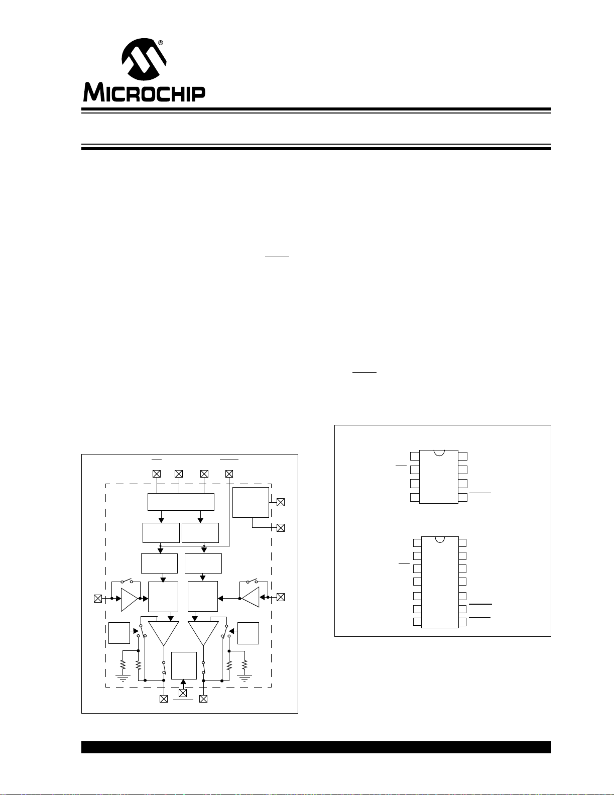
Block Diagram
CS SDI SCK
Interface Logic
Input
Register A
DACA
V
REF
A
Gain
Logic
Register
Buffer
String
DAC
Register B
A
Output
Op Amps
Input
DAC
B
Register
String
DAC
B
LDAC
Power-on
Reset
Buffer
Gain
Logic
V
AV
V
B
DD
SS
REF
Description
The Microchip Technology Inc. MCP492X are 2.7–
5.5V , low-power , low DNL, 12-Bit Digital-to-Analog Converters (DACs) with optional 2x buffered output and SPI
interface.
The MCP492X are DACs that provide high accuracy
and low noise performance for industrial applications
where calibration or compensation of signals (such as
temperature, pressure and humidity) are required.
The MCP492X are available in the extended temperature range and PDIP, SOIC, MSOP and TSSOP
packages.
The MCP492X devices utilize a resistive string architecture, with its inherent advantages of low DNL error,
low ratio metric tem perature coe fficient and fast s ettling
time. These devices are specified over the extended
temperature range. The MCP492X include doublebuffered inputs, allowing simultaneous updates using
the LDAC
pin. These devices also incorporate a
Power-On Reset (POR) circuit to ensure reliable
power-up.
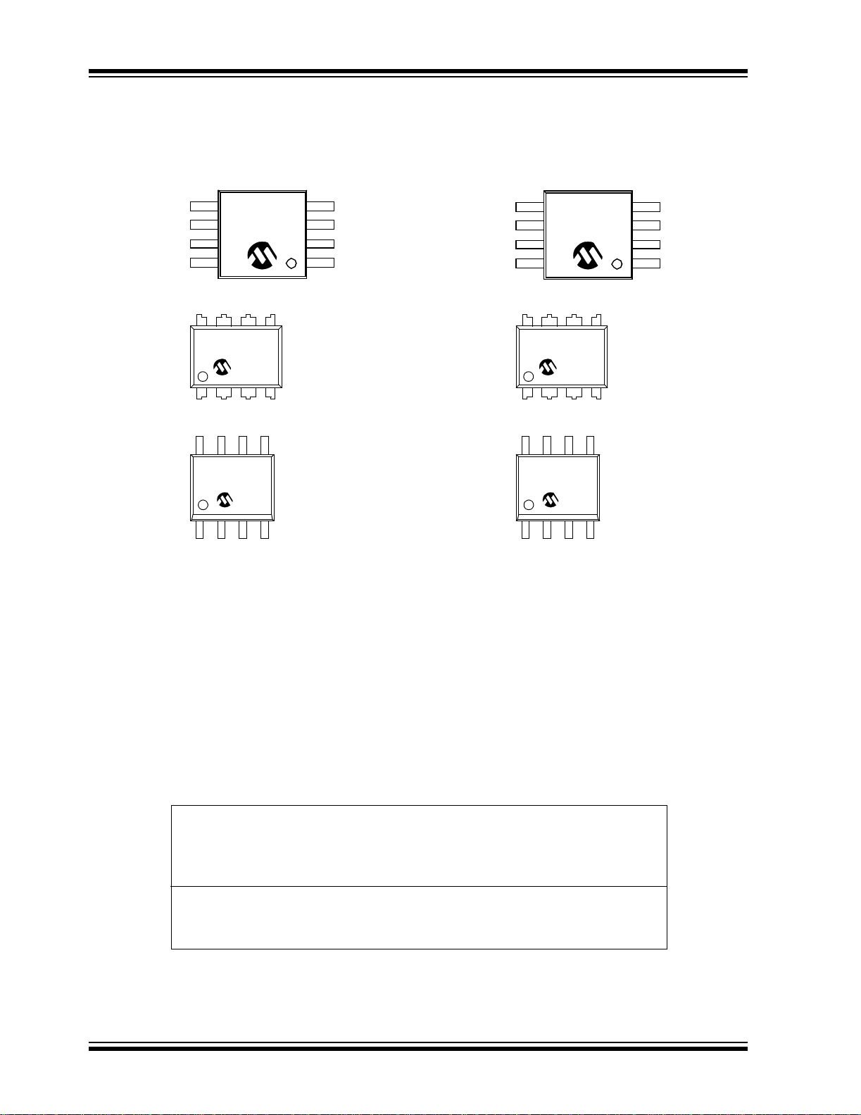
Package Types
8-Pin PDIP, SOIC, MSOP
V
DD
CS
SCK
SDI
14-Pin PDIP, SOIC, TSSOP
V
DD
NC
CS
SCK
SDI
NC
NC
MCP4921
1
2
3
4
1
2
MCP4922
3
4
5
6
7
8
7
6
5
14
13
12
11
10
9
8
V
OUTA
AV
SS
V
REFA
LDAC
V
OUTA
V
REFA
AV
SS
V
REFB
V
OUTB
SHDN
LDAC
Output
Logic
V
OUTA
2004 Microchip Technology Inc. DS21897A-page 1
SHDN
V
OUTB
MCP4921/4922
1.0 ELECTRICAL CHARACTERISTICS
† Notice: Stresses above those listed under “Maximum Rat-
ings” may cause permanent damage to the devic e. This is a
stress rating only and functional operation of the device at
those or any other conditions above those indicated in the
Absolute Maximum Ratings †
operational listings of this specification is not implied. Exposure to maximum rating conditions for extended periods m ay
V
............................................................................................................. 6.5V
DD
All inputs and outputs w.r.t .............AV
–0.3V to VDD+0.3V
SS
affect device reliability.
Current at Input Pins .................. .... .... .. ......... .... .... .. .... .±2 mA
Current at Supply Pins . ..............................................±50 mA
Current at Output Pins .................................. ............ .±2 5mA
Storage temperature.....................................-65°C to +150°C
Ambient temp. with power applied................ - 55°C to +125°C
ESD protection on all pins ...........≥ 4 kV (HBM), ≥ 400V (MM)
Maximum Junction Temperature (T
)..........................+150°C
J
5V AC/DC CHARACTERISTICS
Electrical Specifications: Unless otherwise indicated, V
to GND, C
= 100 pF TA = -40 to +85°C. Typical values at +25°C.
L
Parameters Sym Min Typ Max Units Conditions
Power Requirements
Input Voltage V
Input Current - MCP4921
Input Current - MCP4922
Hardware Shutdown Current I
Software Shutdown Current I
SHDN_SW
Power-on-Reset Threshold V
DD
I
DD
SHDN
POR
2.7 — 5.5
—
—
—0.3 2 µA
—3.3 6 µA
—2.0 — V
DC Accuracy
Resolution n 12 — — Bits
INL Error INL -12 2 12 LSB
DNL DNL -0.75 ±0.2 +0.75 LSB Device is Monotonic
Offset Error V
Offset Error Temperature
Coefficient
V
OS
Gain Error g
Gain Error Temperature
∆G/°C — -3 — ppm/°C
OS
/°C — 0.16 — ppm/°C -45°C to 25°C
E
— ±0.02 1 % of FSR Code 0x000h
— -0.44 — ppm/°C +25°C to 85°C
— -0.10 1 % of FSR Code 0xFFFh, not including offset
Coefficient
Input Amplifier (V
Input Range - Buffered Mode V
Input Range - Unbuffered
REF
Input)
V
REF
REF
0.040 — V
0— VDDV
Mode
Input Impedance R
Input Capacitance -
Unbuffered Mode
Multiplier Mode
C
f
VREF
VREF
VREF
— 165 — kΩ Unbuffered Mode
—7 — pF
— 450 — kH z V
-3 dB Bandwidth
— 400 — kH z V
—-73 — dBV
Multiplier Mode Total Harmonic Distortion
f
THD
VREF
VREF
Note 1: By design, not production tested.
2: Too small to quantify.
= 5V , AV
DD
175
350
SS
350
= 0V, V
= 2.048V , output buf fer gai n (G) = 2x, RL = 5 kΩ
REF
µA Input unbuffered, digital inputs
700
– 0.040 V Note 1
DD
grounded, output unloaded,
code at 0x000
error.
Code = 2048
V
= 0.2v p-p, f = 100 Hz and 1 kHz
REF
= 2.5V ±0.2Vp-p, Unbuffered,
REF
G = 1
= 2.5V ±0.2 Vp-p, Unbuffered,
REF
G = 2
= 2.5V ±0.2Vp-p,
REF
Frequency = 1 kHz
DS21897A-page 2 2004 Microchip Technology Inc.
MCP4921/4922
5V AC/DC CHARACTERISTICS (CONTINUED)
Electrical Specifications: Unless otherwise indicated, V
to GND, C
= 100 pF TA = -40 to +85°C. Typical values at +25°C.
L
Parameters Sym Min Typ Max Units Conditions
Output Amplifier
Output Swing V
Phase Margin
OUT
θm — 66 — degrees
— 0.010
Slew Rate SR — 0.55 — V/µs
Short Circuit Current I
Settling Time t
SC
settling
—15 24 mA
— 4.5 — µs Within 1/2 LSB of final value from 1/4
Dynamic Performance
DAC-to-DAC Crosstalk — 10 — nV-s Note 2
Major Code Transition Glitch — 45 — nV-s 1 LSB change around major carry
Digital Feedthrough — 10 — nV-s Note 2
Analog Crosstalk — 10 — nV-s Note 2
Note 1: By design, not production tested.
2: Too small to quantify.
= 5V , AV
DD
to V
DD
– 0.040
SS
= 0V, V
= 2.048V , output buf fer gain (G) = 2x, RL = 5 kΩ
REF
— Accuracy is better than 1 LSB for
V
= 10 mV to (V
OUT
to 3/4 full-scale range
(0111...1111 to 1000. ..0000)
– 40 mV)
DD
3V AC/DC CHARACTERISTICS
Electrical Specifications: Unless otherwise indicated, V
R
= 5 kΩ to GND, CL = 100 pF TA = -40 to +85°C. Typical values at 25°C
L
Parameters Sym Min Typ Max Units Conditions
Power Requirements
Input Voltage V
Input Current - MCP4921
Input Current - MCP4922
Hardware Shutdown Current I
Software Shutdown Current I
SHDN_SW
Power-On Reset threshold V
DD
I
DD
SHDN
POR
2.7 — 5.5
—
—
—0.25 2 µA
—2 6 µA
—2.0 — V
DC Accuracy
Resolution n 12 — — Bits
INL Error INL -12 ±3 +12 LSB
DNL DNL -0.75 ±0.3 +0.75 LSB Device is Monotonic
Offset Error V
Offset Error Temperature
V
Coefficient
Gain Error g
Gain Error Temperature
∆G/°C — -3 — ppm/°C
OS
/°C — 0.5 — ppm/°C -45°C to 25°C
OS
E
— ±0.02 1 % of FSR Code 0x000h
— -0.77 — ppm/°C +25°C to 85°C
— -0.15 1 % of FSR Code 0xFFFh, not including offset
Coefficient
Input Amplifier (V
Input Range - Buffered Mode V
Input Range - Unbuffered
Mode
Input Impedance R
REF
Input)
REF
V
REF
VREF
0.040 — VDD-0.040 V Note 1
0—VDDV
— 165 — kΩ Unbuffered Mode
Note 1: By design, not production tested.
2: Too small to quantify.
= 3V, AV
DD
125
250
SS
250
500
= 0V, V
= 2.048V external, output buffer gain (G) = 1x,
REF
µA Input unbuffered, digital inputs
grounded, output unloaded,
code at 0x000
error.
Code = 2048,
= 0.2v p-p, f = 100 Hz and 1 kHz
V
REF
2004 Microchip Technology Inc. DS21897A-page 3
MCP4921/4922
3V AC/DC CHARACTERISTICS (CONTINUED)
Electrical Specifications: Unless otherwise indicated, V
= 5 kΩ to GND, CL = 100 pF TA = -40 to +85°C. Typical values at 25°C
R
L
Parameters Sym Min Typ Max Units Conditions
Input Capacitance –
C
VREF
—7 — pF
Unbuffered Mode
Multiplier Mode
-3 dB Bandwidth
Multiplier Mode –
Total Harmonic Distortion
f
f
THD
VREF
VREF
VREF
— 440 — kHz V
— 390 — kHz V
—-73 — dBV
Output Amplifier
Output Swing V
Phase Margin
OUT
θm — 66 — degrees
— 0.010
Slew Rate SR — 0.55 — V/µs
Short Circuit Current I
Settling Time t
SC
settling
—14 24 mA
— 4.5 — µs Within 1/2 LSB of final value from 1/4
Dynamic Performance
DAC-to-DAC Crosstalk — 10 — nV-s Note 2
Major Code Transition Glitch — 45 — nV-s 1 LSB change around major carry
Digital Feedthrough — 10 — nV-s Note 2
Analog Crosstalk — 10 — nV-s Note 2
Note 1: By design, not production tested.
2: Too small to quantify.
= 3V, AV
DD
to V
DD
– 0.040
SS
= 0V, V
= 2.048V external, output buffer gain (G) = 1x,
REF
= 2.048V ±0.1 Vp-p, unbuffered,
REF
G = 1
= 2.048V ±0.1 Vp-p, unbuffered,
REF
G = 2
= 2.5V ±0.1 Vp-p,
REF
Frequency = 1 kHz
— Accuracy is better than 1 LSB for
V
= 10 mV to (VDD – 40 mV )
OUT
to 3/4 full-scale range
(0111...1111 to 1000...0000)
5V EXTENDED TEMPERATURE SPECIFICATIONS
Electrical Specifications: Unless otherwise indicated, V
to GND, C
= 100 pF. Typical values at +125°C by characterization or simulation.
L
Parameters Sym Min Typ Max Units Conditions
Power Requirements
Input Voltage V
Input Current - MCP4921
Input Current - MCP4922
Hardware Shutdown Current I
Software Shutdown Current I
SHDN_SW
Power-On Reset threshold V
DD
I
DD
SHDN
POR
2.7 — 5.5
—
—
—1.5— µA
—5— µA
—1.85— V
DC Accuracy
Resolution n 12 — — Bits
INL Error INL — ±4 — LSB
DNL DNL — ±0.25 — LSB Device is Monotonic
Offset Error V
Offset Error Temperature
V
Coefficient
OS
/°C — -5 — ppm/°C +25°C to +125°C
OS
— ±0.02 — % of FSR Code 0x000h
Note 1: By design, not production tested.
2: Too small to quantify.
= 5V , AV
DD
200
400
SS
—
—
= 0V , V
= 2.048V, output buf fer gain (G) = 2x, RL = 5 kΩ
REF
µA Input unbuffered, digital inputs
grounded, output unloaded,
code at 0x000
DS21897A-page 4 2004 Microchip Technology Inc.
MCP4921/4922
5V EXTENDED TEMPERATURE SPECIFICATIONS (CONTINUED)
Electrical Specifications: Unless otherwise indicated, V
to GND, C
= 100 pF. Typical values at +125°C by characterization or simulation.
L
Parameters Sym Min Typ Max Units Conditions
Gain Error g
Gain Error Temperature
∆G/°C — -3 — ppm/°C
E
— -0.10 — % of FSR Co de 0xFFFh, not including offset
Coefficient
Input Amplifier (V
Input Range - Buffered Mode V
Input Range - Unbuffered
Mode
Input Impedance R
Input Capacitance -
Unbuffered Mode
Multiplying Mode
REF
Input)
V
C
f
REF
REF
VREF
VREF
VREF
— 0.040 to
0—VDDV
— 174 — kΩ Unbuffered Mode
—7— pF
— 450 — kHz V
-3 dB Bandwidth
— 400 — kHz V
——— dBV
Multiplying Mode - Total
Harmonic Distortion
f
THD
VREF
VREF
Output Amplifier
Output Swing V
Phase Margin
OUT
θm — 66 — degrees
— 0.010 to
Slew Rate SR — 0.55 — V/µs
Short Circuit Current I
Settling Time t
SC
settling
—17— mA
— 4.5 — µ s Within 1/2 LSB of final value from 1/4
Dynamic Performance
DAC to DAC Crosstalk — 10 — nV-s Note 2
Major Code Transition Glitch — 45 — nV-s 1 LSB change around major carry
Digital Feedthrough — 10 — nV-s Note 2
Analog Crosstalk — 10 — nV-s Note 2
Note 1: By design, not production tested.
2: Too small to quantify.
= 5V , AV
DD
V
DD
0.040
V
DD
0.040
–
SS
= 0V , V
= 2.048V , output buffer gain (G) = 2x, RL = 5 kΩ
REF
error
—VNote 1
-
Code = 2048,
V
= 0.2v p-p, f = 100 Hz and 1 kHz
REF
= 2.5V ±0.1 Vp-p, Unbuffered,
REF
G=1
= 2.5V ±0.1 Vp-p, Unbuffered,
REF
G = 2
= 2.5V ±0.1Vp-p,
REF
Frequency = 1 kHz
— Accuracy is better than 1 LSB for
V
= 10 mV to (V
OUT
to 3/4 full-scale range
(0111...1111 to 1000...0000)
– 40 mV)
DD
2004 Microchip Technology Inc. DS21897A-page 5
MCP4921/4922
AC CHARACTERISTICS (SPI TIMING SPECIFICATIONS)
Electrical Specifications: Unless otherwise indicated, VDD= 2.7V – 5.5V, TA= -40 to +125°C.
Typical values are at +25°C.
Parameters Sym Min Typ Max Units Conditions
Schmitt Trigger High-Level
V
0.7 V
IH
——V
DD
Input Voltage (All digital input
pins)
Schmitt Trigger Low-Level
V
IL
——0.2V
Input Voltage
(All digital input pins)
Hysteresis of Schmitt Trigger
V
HYS
—0.05VDD—
Inputs
Input Leakage Current I
LEAKAGE
Digital Pin Capacitance
(All inputs/outputs)
C
Clock Frequency F
Clock High Time t
Clock Low Time t
Fall to First Rising CLK
CS
t
CIN,
OUT
CLK
HI
LO
CSSR
-1 — 1 µASHDN = LDAC = CS = SDI =
—10—pFV
——20MHzT
15 — — ns Note 1
15 — — ns Note 1
40 — — ns Applies only when CS falls with
Edge
Data Input Setup Time t
Data Input Hold Time t
SCK Rise to CS
Rise Hold
t
CHS
SU
HD
15 — — ns Note 1
10 — — ns Note 1
15 — — ns Note 1
Time
CS
High Time t
Pulse Width t
LDAC
Setup Time t
LDAC
SCK Idle Time before CS
Fall t
CSH
LD
LS
IDLE
15 — — ns Note 1
100 — — ns Note 1
40 — — ns Note 1
40 — — ns Note 1
Note 1: By design and characterization, not production tested.
V
D
D
SCK + V
= 5.0V, TA = +25°C,
DD
f
= 1 MHz (Note 1)
cLK
= +25°C (Note 1)
A
= VDD or AV
REF
SS
CLK high. (Note 1)
t
CSH
CS
t
IDLE
t
LS
t
LD
SCK
LDAC
Mode 1,1
Mode 0,0
SI
t
CSSR
t
SU
MSB in
t
t
LO
HI
t
HD
LSB in
t
CHS
FIGURE 1-1: SPI™ Input Timing.
DS21897A-page 6 2004 Microchip Technology Inc.
MCP4921/4922
TEMPERATURE CHARACTERISTICS
Electrical Specifications: Unless otherwise indicated, VDD= +2.7V to +5.5V, AVSS= GND.
Parameters Sym Min Typ Max Units Conditions
Temperature Ranges
Specified Temperature Range T
Operating Temperature Range T
Storage Temperature Range T
A
A
A
Thermal Package Resistances
Thermal Resistance, 8L-PDIP θ
Thermal Resistance, 8L-SOIC θ
Thermal Resistance, 8L-MSOP θ
Thermal Resistance, 14L-PDIP θ
Thermal Resistance, 14L-SOIC θ
Thermal Resistance, 14L-TSSOP θ
JA
JA
JA
JA
JA
JA
Note 1: The MCP492X family of DACs operate over this extended temperature range, but with reduced
performance. Operation in this range must not cause T
150°C.
-40 — +125 °C
-40 — +125 °C Note 1
-65 — +150 °C
—85—°C/W
—163—°C/W
—206—°C/W
—70—°C/W
—120—°C/W
—100—°C/W
to exceed the Maximum Junction Temperature of
J
2004 Microchip Technology Inc. DS21897A-page 7
MCP4921/4922
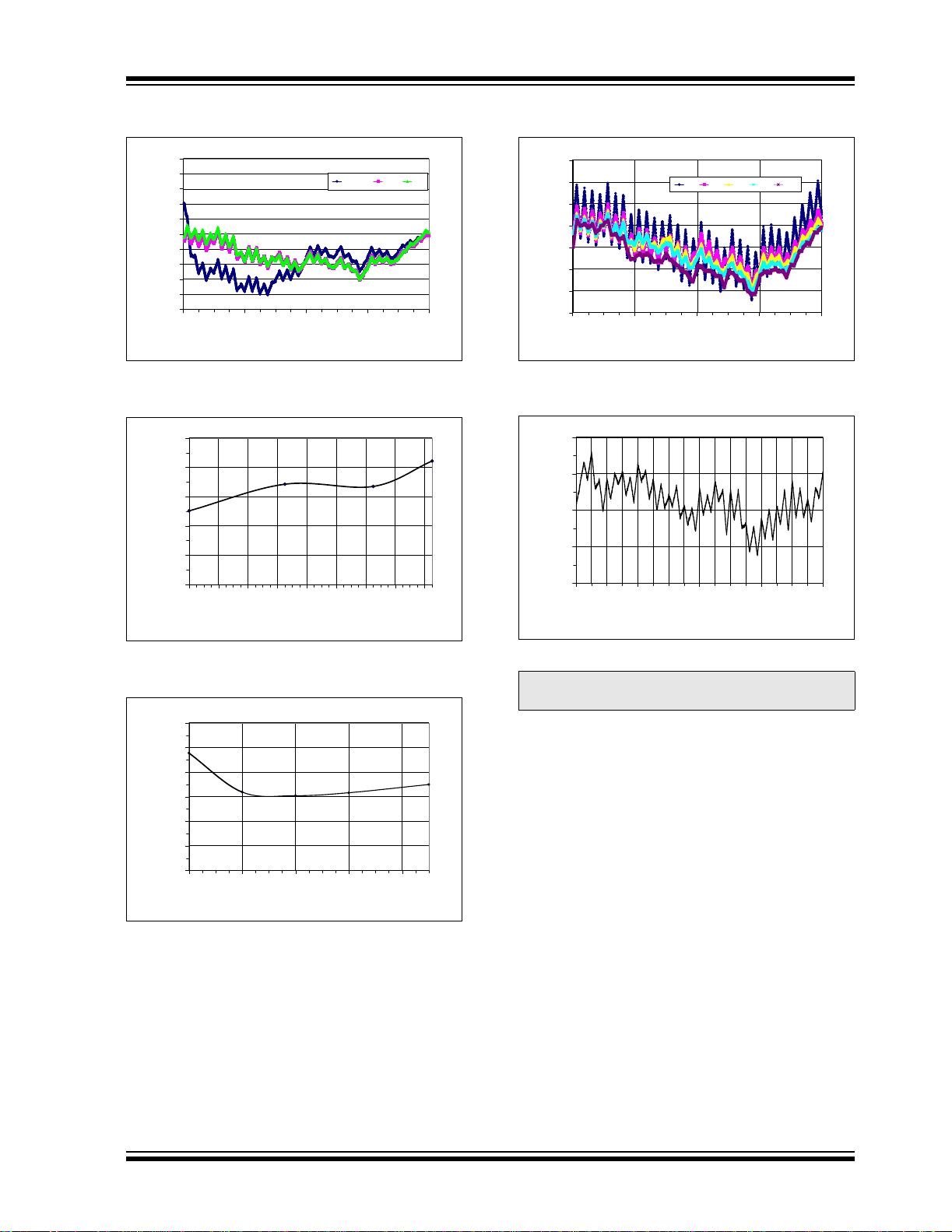
2.0 TYPICAL PERFORMANCE CURVES
Note: The graphs and tables provid ed fol low i ng thi s n ote are a statistical summary based on a l im ite d n um ber of
samples and are provided for informational purposes only. The performance characteristics listed herein
are not tested or guaranteed. In some graphs or tables, the data presented may be outside the specified
operating range (e.g., outside specified power supply range) and therefore outside the warranted range.
Note: Unless otherwi se indi cated, TA = +25°C, VDD = 5V , AVSS = 0V, V
0.3
0.2
0.1
0
DNL (LSB)
-0.1
-0.2
-0.3
0 1024 2048 3072 4096
Code (Decimal)
FIGURE 2-1: DNL vs. Code.
Absolute DNL (LSB)
FIGURE 2-4: Absolute DNL vs. Ambient Temperature.
0.2
0.1
0
DNL (LSB)
-0.1
-0.2
0 1024 2048 3072 4096
Code (Decimal)
125C 85C 25C
Absolute DNL (LSB)
= 2.048V , G ain = 2, RL = 5 kΩ, CL = 100 pF .
REF
0.0766
0.0764
0.0762
0.076
0.0758
0.0756
0.0754
0.0752
0.075
-40 -20 0 20 40 60 80 100 120
Ambient Temperature (ºC)
0.35
0.3
0.25
0.2
0.15
0.1
0.05
0
12345
Voltage Reference (V)
FIGURE 2-2: DNL vs. Code and Ambient Temperature.
0.4
0.3
0.2
0.1
0
-0.1
DNL (LSB)
-0.2
-0.3
-0.4
0 1024 2048 3072 4096
Code (Decimal)
FIGURE 2-3: DNL vs. Code and V
1 2 3 4 5.5
.
REF
FIGURE 2-5: Absolute DNL vs. Voltage Reference.
Gain=1.
DS21897A-page 8 2004 Microchip Technology Inc.
MCP4921/4922
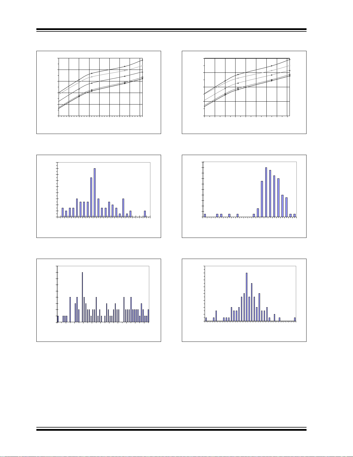
Note: Unless otherwi se indic ated, TA = +25°C, VDD = 5V , AVSS = 0V, V
5
4
3
2
1
0
-1
INL (LSB)
-2
-3
-4
-5
0 1024 2048 3072 4096
Code (Decimal)
FIGURE 2-6: INL vs. Code and Ambient
Ambient Temperature
125C 85 25
INL (LSB)
FIGURE 2-9: INL vs. Code and V
Temperature.
2.5
2
1.5
1
0.5
Absolute INL (LSB)
0
-40 -20 0 20 40 60 80 100 120
Ambient Temperature (ºC)
INL (LSB)
= 2.048V , G ain = 2, RL = 5 kΩ, CL = 100 pF .
REF
3
2
1
0
-1
-2
-3
-4
0 1024 2048 3072 4096
Code (Decimal)
2
0
-2
-4
-6
0 1024 2048 3072 4096
Code (Decimal)
V
REF
1 2 3 4 5.5
REF
.
FIGURE 2-7: Absolute INL vs. Ambient Temperature.
3
2.5
2
1.5
1
Absolute INL (LSB)
0.5
0
12345
Voltage Reference (V)
FIGURE 2-8: Absolute INL vs. V
REF
.
FIGURE 2-10: INL vs. Code.
Note: Single device graph (Figure 2-10) for
illustration of 64 code effect.
2004 Microchip Technology Inc. DS21897A-page 9
MCP4921/4922
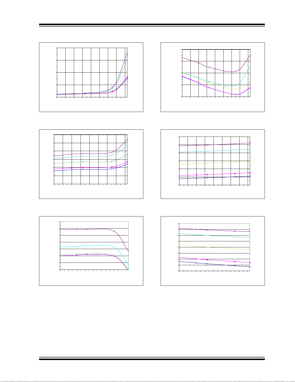
Note: Unless otherwise indicated, TA = +25°C, VDD = 5V, AVSS = 0V, V
210
190
170
(µA)
DD
I
150
130
110
-40-200 20406080100120
Ambient Temperature (°C)
FIGURE 2-11: MCP4921 IDD vs. Ambient
Temperature and V
18
16
14
12
10
8
Occurrence
6
4
2
0
143
145
147
149
DD
.
151
IDD (µA)
153
155
157
159
161
163
165
5.5V
5.0V
4.0V
3.0V
2.7V
V
167
DD
(µA)
DD
I
FIGURE 2-14: MCP4922 I
Temperature and V
Occurrence
= 2.048V, Gain = 2.
REF
400
350
300
250
200
-40 -20 0 20 40 60 80 100 120
20
18
16
14
12
10
8
6
4
2
0
Ambient Temperature (ºC)
DD
215
225
235
245
.
255
IDD (µA)
265
vs. Ambient
DD
275
285
295
305
315
5.5V
5.0V
4.0V
3.0V
2.7V
V
DD
325
FIGURE 2-12: MCP4921 I
(V
= 2.7V).
DD
9
8
7
6
5
4
3
Occurrence
2
1
0
151 156 161 166 171 176 181 186 191 196 201
IDD (µA)
FIGURE 2-13: MCP4921 I
(V
= 5.0V).
DD
Histogram
DD
Histogram
DD
FIGURE 2-15: MCP4922 I
(V
= 2.7V).
DD
16
14
12
10
8
6
Occurrence
4
2
0
250
265
280
295
310
325
340
IDD (µA)
FIGURE 2-16: MCP4922 I
(V
= 5.0V).
DD
Histogram
DD
355
370
385
Histogram
DD
400
415
DS21897A-page 10 2004 Microchip Technology Inc.
MCP4921/4922
V
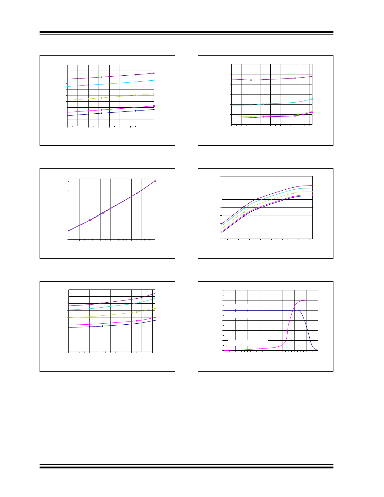
Note: Unless otherwi se indic ated, TA = +25°C, VDD = 5V , AVSS = 0V, V
2
5.5V
1.5
(µA)
1
SHDN
I
0.5
0
-40 -20 0 20 40 60 80 100 120
Ambient Temperature (ºC)
FIGURE 2-17: Hardware Shutdown
Current vs. Ambient Temperature and V
6
5
4
(µA)
3
2
SHDN_SW
I
1
0
-40 -20 0 20 40 60 80 100 120
Ambient Temperature (ºC)
DD
5.0V
4.0V
3.0V
2.7V
V
.
5.5V
5.0V
4.0V
3.0V
2.7V
V
DD
Gain Error (%)
FIGURE 2-20: Gain Error vs. Ambient
Temperature and V
DD
Hi Threshold (V)
IN
V
= 2.048V , G ain = 2, RL = 5 kΩ, CL = 100 pF .
REF
-0.08
-0.1
-0.12
-0.14
-0.16
-40 -20 0 20 40 60 80 100 120
Ambient Temperature (ºC)
.
DD
4
3.5
3
2.5
2
1.5
1
-40 -20 0 20 40 60 80 100 120
Ambient Temperature (ºC)
V
DD
5.5V
5.0V
4.0V
3.0V
2.7V
V
5.5V
5.0V
4.0V
3.0V
2.7V
DD
FIGURE 2-18: Software Shutdown Current
vs. Ambient Temperature and V
0.12
0.1
0.08
0.06
0.04
0.02
Offset Error (%)
0
-0.02
-40 -20 0 20 40 60 80 100 120
Ambient Temperature (ºC)
DD
.
V
DD
5.5V
5.0V
4.0
3.0V
2.7V
FIGURE 2-19: Offset Error vs. Ambient
Temperature and V
DD
.
FIGURE 2-21: V
High Threshold vs
IN
Ambient Temperature and V
1.6
1.5
1.4
1.3
1.2
1.1
Low Threshold (V)
IN
1
V
0.9
0.8
-40 -20 0 20 40 60 80 100 120
FIGURE 2-22: V
Ambient Temperature (ºC)
Low Threshold vs
IN
Ambient Temperature and V
DD
DD
.
V
DD
5.5V
5.0V
4.0V
3.0V
2.7V
.
2004 Microchip Technology Inc. DS21897A-page 11
MCP4921/4922
V
Note: Unless otherwi se indi cated, TA = +25°C, VDD = 5V , AVSS = 0V, V
2.5
2.25
2
1.75
1.5
1.25
1
Hysteresis (V)
SPI
0.75
_
IN
0.5
V
0.25
0
-40 -20 0 20 40 60 80 100 120
Ambient Temperature (ºC)
FIGURE 2-23: Input Hysteresis vs. Ambient
Temperature and V
175
170
Impedance
165
(kOhm)
160
REF_UNBUFFERED
V
155
-40 -20 0 20 40 60 80 100 120
.
DD
Ambient Temperature (ºC)
V
DD
5.5V
5.0V
4.0V
3.0V
2.7V
5.5V -
2.7V
V
DD
)(V)
SS
Limit (Y-AV
OUT_LOW
V
FIGURE 2-26: V
Temperature and V
(mA)
OUT_HI_SHORTED
I
= 2.048V , G ain = 2, RL = 5 kΩ, CL = 100 pF .
REF
0.0045
0.004
0.0035
0.003
0.0025
0.002
0.0015
-40 -20 0 20 40 60 80 100 120
Ambient Temperature (ºC)
Low Limit vs. Ambient
OUT
.
DD
18
17
16
15
14
13
12
11
10
-40 -20 0 20 40 60 80 100 120
Ambient Temperature (ºC)
V
5.5V
5.0V
4.0V
3.0V
2.7V
V
5.5V
5.0V
4.0V
3.0V
2.7V
DD
DD
FIGURE 2-24: V
Input Impedance vs.
REF
Ambient Temperature and V
0.045
0.04
0.035
-Y)(V)
0.03
DD
0.025
0.02
Limit (V
0.015
0.01
OUT_HI
V
0.005
0
-40 -20 0 20 40 60 80 100 120
Ambient Temperature (ºC)
FIGURE 2-25: V
Temperature and V
High Limit vs. Ambient
OUT
.
DD
DD
FIGURE 2-27: I
.
5.5V
5.0V
4.0
3.0V
2.7V
V
DD
Ambient Temperature and V
6.0
(V)
OUT
V
5.0
4.0
3.0
2.0
1.0
0.0
V
=4.0
REF
Output Shorted to V
Output Shorted to V
0246810121416
FIGURE 2-28: I
High Short vs.
OUT
I
OUT
OUT
DD
SS
(mA)
vs V
DD
.
OUT
. Gain = 1.
DS21897A-page 12 2004 Microchip Technology Inc.

MCP4921/4922
Note: Unless otherwi se indic ated, TA = +25°C, VDD = 5V , AVSS = 0V, V
V
OUT
V
OUT
SCK
LDAC
Time (1 µs/div)
FIGURE 2-29: V
V
OUT
SCK
Rise Time 100%.
OUT
LDAC
FIGURE 2-32: V
V
OUT
SCK
= 2.048V , G ain = 2, RL = 5 kΩ, CL = 100 pF .
REF
Time (1 µs/div)
Rise Time 25% - 75%
OUT
LDAC
Time (1 µs/div)
FIGURE 2-30: V
V
OUT
SCK
LDAC
Time (1 µs/div)
FIGURE 2-31: V
Fall Time.
OUT
Rise Time 50%.
OUT
LDAC
Time (1 µs/div)
FIGURE 2-33: V
Rise Time Exit
OUT
Shutdown.
Ripple Rejection (dB)
Frequency (Hz)
FIGURE 2-34: PSRR vs. Frequency.
2004 Microchip Technology Inc. DS21897A-page 13

MCP4921/4922
))
VOUT
Note: Unless otherwise in dic ated, TA = +25°C, VDD = 5V , AVSS = 0V, V
20
G = 1
G = 2
2
9
76
3
2
D = 160
D = 416
D = 672
D = 928
D = 1184
D = 1440
D = 1696
D = 1952
D = 2208
D = 2464
D = 2720
D = 2976
D = 3232
D = 3488
D = 3744
3
32
– q
VREF
q
-135
-180
FIGURE 2-37: Phase Shift.
3
4
7
88
44
0
-2
-4
-6
-8
Attenuation (dB)
-10
-12
100 1,000
Frequency (kHz)
FIGURE 2-35: Multiplier Mode Bandwidth.
Figure 2-35 calculation:
Attenuation (dB) = 20 log (V
600
580
560
540
520
500
480
460
Bandwidth (kHz)
440
420
400
1
4
6
9
6
0
1
1
7
2
1
6
2
8
84
Worst Case Codes (decimal)
OUT/VREF
1
4
40
) – 20 log (G(D/4096
1
1
2
2
6
96
2
9
2
4
7
52
08
64
= 2.50V, Gain = 2, RL = 5 kΩ, CL = 100 pF.
REF
0
-45
-90
100 1,000
Frequency (kHz)
D = 160
D = 416
D = 672
D = 928
D = 1184
D = 1440
D = 1696
D = 1952
D = 2208
D = 2464
D = 2720
D = 2976
D = 3232
D = 3488
D = 3744
FIGURE 2-36: -3 db Bandwidth vs. Worst
Codes.
DS21897A-page 14 2004 Microchip Technology Inc.

3.0 PIN DESCRIPTIONS
The descriptions of the pins are listed in Table 3-1.
TABLE 3-1: PIN FUNCTION TABLE
MCP4921/4922
MCP4921
Pin No.
11V
— 2 NC No Connection
23CS
3 4 SCK Serial Clock Input
4 5 SDI Serial Data Input
— 6 NC No Connection
— 7 NC No Connection
58LDAC
— 9 SHDN
—10V
—11V
712AV
613V
814V
MCP4922
Pin No.
Symbol Function
DD
OUTB
REFB
SS
REFA
OUTA
Positive Power Supply Input (2.7V to 5.5V)
Chip Select Input
Syncronization input used to transfer DAC settings from serial
latches to the output latches.
Hardware Shutdown Input
DACB Output
DACB Voltage Input (AV
Analog ground
DACA Voltage Input (AVSS to VDD)
DACA Output
3.1 Positive Power Supply Input (VDD)
VDD is the positive power supply input. The input power
supply is relative to AV
5.5V. A decoupling capacitor o n V
to achieve maximum performance.
and can range from 2. 7V to
SS
is recommended
DD
3.2 Chip Select (CS)
CS is the chip select i nput, which require s an active-low
signal to enable serial clock and data functions.
3.3 Serial Clock Input (SCK)
SCK is the SPI compatible seri al clock input .
3.4 Serial Data Input (SDI)
SDI is the SPI compatible serial data input.
to VDD)
SS
3.6 Hardware Shutdown Input (SHDN)
SHDN is the hardware s hutdown input that requires an
active-low input signal to configure the DACs in their
low-power Standby mode.
3.7 DACx Outputs (V
V
and V
OUTA
amplifier drives these pins with a range of A V
are DAC outputs. The DAC output
OUTB
OUTA
, V
OUTB
SS
)
to VDD.
3.8 DACX Voltage Reference Inputs
(V
V
and V
REFA
The analog signal on these pins is utilized to s et the reference voltage on the string DAC. The input signa l can
range from AV
, V
REFA
are DAC voltag e reference inputs.
REFB
to VDD.
SS
REFB
)
3.5 Latch DAC Input (LDAC)
LDAC (the latch DAC syncronization input) transfers
the input l atch registers to the DAC register s (output
latches) when low. Can also be tied low if transfer on
the rising edge of CS
2004 Microchip Technology Inc. DS21897A-page 15
is desired.
3.9 Analog Ground (AVSS)
AVSS is the analog ground pin.

MCP4921/4922
4.0 GENERAL OVERVIEW
The MCP492X devices are voltage ou tput string DA Cs.
These devices include input amplifiers, rail-to-rail output amplifiers, reference buffers, shutdown and resetmanagement circuitry. Serial communication conforms
to the SPI protocol. The MC P4 92X o per ates fro m 2 .7V
to 5.5V supplies.
The coding of these devices is straight binary and the
ideal output voltage is given by Equation 4-1, where G
is the selected gain (1x or 2x), D
input value and n represents the number of bits of
resolution (n = 12).
EQUATION 4-1: LSB SIZE
V
=
OUT
1 LSB is the ideal voltage difference between two
successive codes. Table 4-1 illustrates how to calculate
LSB.
TABLE 4-1: LSB SIZES
Device V
MCP492X External V
MCP492X External V
, GAIN LSB SIZE
REF
REF
REF
represents the digita l
N
V
REFGDN
-------------------------
n
2
, 1x V
REF
, 2x 2 V
/4096
REF
/4096
INL < 0
111
Actual
110
transfer
function
101
Digital
100
Input
Code
011
010
Ideal transfer
function
001
000
INL < 0
DAC Output
FIGURE 4-1: INL Accu r acy.
4.0.2 DNL ACCURACY
DNL error is the measure of variations in code widths
from the ideal code width. A DNL error of zero would
imply that every code is exactly 1 LSB wide.
4.0.1 INL ACCURACY
INL error for these devices is the maximum deviation
between an actual code transition point and its corresponding ideal transition point once offset and gain
errors have been removed. These endpoints are from
0x000 to 0xFFF. Refer to Figure 4-1.
Positive INL means transition(s) later than ideal.
Negative INL means transition(s) earlier than ideal.
111
110
Actual
transfer
101
function
Digital
Input
Code
100
011
010
001
000
Ideal transfer
function
Wide code, > 1 LSB
Narrow code < 1 LSB
DAC Output
FIGURE 4-2: DNL Accuracy.
4.0.3 OFFSET ERROR
Offset error is the deviation from zero voltage output
when the digital input code is zero.
4.0.4 GAIN ERROR
Gain error is the deviation from the ideal output,
– 1 LSB, excluding the effects of offset error.
V
REF
DS21897A-page 16 2004 Microchip Technology Inc.

MCP4921/4922
4.1 Circuit Descriptions
4.1.1 OUTPUT AMPLIFIERS
The DACs’ outputs are buffered with a low-power,
precision CMOS amplifier. This amplifier provides low
offset volt ag e a nd l ow noise. The output stage enables
the device to operate with output voltages close to the
power supply rails. Refer to Section1.0 “Electrical
Characteristics” for range and load conditions.
In addition to res istive load driv ing cap ability, the amplifier will also drive high capacitive loads without oscillation. The amplifiers’ strong outputs allow V
used as a programmable voltage reference in a
system.
Selecting a gain of 2 reduces the bandwidth of the
amplifier in Multiplying mode. Refer to Section 1.0
“Electrical Char acter istics ” for the Multiplying mode
bandwidth for given load conditions.
4.1.1.1 Programmable Gain Block
The rail-to-rail output amplifier has configurable gain
allowing optimal full-scale outputs for differing voltage
reference inputs. The output amplifier gain has two
selections , a gai n of 1 V/V (GA
(GA
= 0).
= 1) or a gain of 2 V/V
The output range is ide ally 0.000V to 4095/4096 * V
when G = 1, and 0.000 to 4095/4096 * V
G = 2. The default value for this bit is a gain of 2, yielding an ideal fu ll-s cale output of 0.000 V to 4. 096V when
utilizing a 2.048V V
. Note that the near rail-to-rail
REF
CMOS output buffer’s ability to approach AV
V
establish practical range limitations. The output
DD
swing specifica tion i n Sectio n 1.0 “Electrical Charac-
teristics” defines the range for a given load condition.
4.1.2 VOLTAGE REFERENCE
AMPLIFIERS
The input buffer amplifiers for the MCP492X devices
provide low offset voltage and low noise. A configuration bit for each DAC allows the V
input to bypass
REF
the input buffer amplifiers, achieving a Buffered or
Unbuffered mode. The default value for this bit is
unbuffered. Buffered mode provides a very high input
impedance, with only minor limitations on the input
range and frequency response. Unbuffered mode
provides a wide input range (0V to V
), with a ty p ic a l
DD
input impedance of 165 kΩ w/7 pF.
4.1.3 POWER-ON RESET CIRCUIT
The Power-On Reset (POR) circuit ensures that the
DACs power-up with SHDN
devices will continue to have a high-impedance output
until a valid write command is performe d to either of th e
DAC registers and the LDAC
threshold.
= 0 (high-impedance). The
pin meets the input low
OUT
REF
to be
when
and
SS
REF
If the power supply voltage is less than the POR
threshold (V
= 2.0V, typical), the DACs will be held
POR
in their reset state. They will remain in that state until
VDD > V
and a subsequent write command is
POR
received.
Figure 4-3 shows a typical power supply transient
pulse and the duration required to cause a reset to
occur, as well as the relationship between the duration
and trip voltage. A 0.1 µF decoupling capacitor
mounted as close as possible to the V
pin provides
DD
additional transient immunity.
5V
V
POR
VDD - V
POR
Transient Duration
Supply Voltages
Time
10
8
6
4
2
Transients below the curve
Transient Duration (µs)
will NOT cause a reset
0
TA = +25°C
Transients above the curve
will cause a reset
12345
– V
POR
(V)
V
DD
FIGURE 4-3: Typical Transient Response.
4.1.4 SHUTDOWN MODE
Shutdown mode can be entered by using either hardware or software commands. The hardware pin
) is only available on the MCP4922. During
(SHDN
Shutdown mode, the supply current is isolated from
most of the internal circuitry. The serial interface
remains active, thus allowing a write command to
bring the device out of Shutdown mode. When the
output amplifiers are shut down, the feedback resistance (typically 500 kΩ) produces a high-impedance
path to AV
mode until the SHDN
command with S
When a DAC is changed from Shutdown to Active
mode, the output settling time takes < 10 µs, but
greater than the standard Active mode settling time
(4.5 µs).
. The device will remain in Shutdown
SS
pin is brought high and a write
D = 1 is latched into the device.
2004 Microchip Technology Inc. DS21897A-page 17

MCP4921/4922
5.0 SERIAL INTERFACE
5.2 Write Command
The write command is initiated by driving the CS pin
5.1 Overview
The MCP492X family is designed to interface directly
with the Serial Peripheral Interface (SPI) port, available
on many microcontrollers, and supports Mode 0,0 and
Mode 1,1. Comm ands and da ta are se nt t o the de vice
via the SDI pin, with dat a being clock ed-in on the ri sing
edge of SCK. The co mmunica tions a re unidi rectio nal
and, thus, data cannot be read out of the MCP492X.
The CS
command. The write c omm an d c on sis t s of 16 bits and
is used to configure the DAC’s cont rol and data latc hes.
Register 5-1 details the input registers used to configure and load the DACA and DACB registers. Refer to
Figure 1-1 and Section 1.0 “Electrical Characteris-
tics” AC Electrical Characteristics table for detailed
input and output timing sp ecifications for bo th Mode 0,0
and Mode 1,1 operation.
pin must be held low for the duratio n of a wri te
low, fo llowed b y clocking the four con figuration bit s an d
the 12 data bits into the SDI pin on the rising edge of
SCK. The CS
pin is then raised, causing the data to
be latched into the se le cte d D AC’s input registers. The
MCP492X utilizes a double-buffered latch structure to
allow both DAC
syncronized with the LDAC
pin achieving a low state, the values held in the
LDAC
’s and DACB’s outputs to be
A
pin, if desired. Upon the
DAC’s input registers are transferred into the DACs’
output registers. The out puts will transition to the value
and held in the DAC
register.
X
All writes to the MCP492X are 16-bit words. Any
clocks past 16 will be ignored. The most significant
four bits are configuration bits. The remaining 12 bits
are data bits. No data can be transferred into the
device with CS
high. This transfer will only occur if 16
clocks have been transferred into the device. If the rising edge of CS
occurs prior, shifting of data into the
input registers will be aborted.
REGISTER 5-1: WRITE COMMAND REGISTER
Upper Half:
W-x W-x W-x W-0 W-x W-x W-x W-x
/B BUF GA SHDN D11 D10 D9 D8
A
bit 15 bit 8
Lower Half:
W-x W-x W-x W-x W-x W-x W-x W-x
D7 D6 D5 D4
D3 D2 D1 D0
bit 7 bit 0
bit 15 A/B: DACA or DACB Select bit
1 = Write to DAC
0 = Write to DAC
bit 14 BUF: V
1 = Buffe red
0 = Unbuffered
bit 13 GA
: Output Gain Select bit
1 =1x (V
0 =2x (V
bit 12 SHDN
1 = Output Power Down Control bit
0 = Output buffer disabled, Output is high impedance
REF
OUT
OUT
: Output Power Down Control bit
B
A
Input Buffer Control bit
= V
= 2 * V
* D/4096)
REF
REF
* D/4096)
bit 11-0 D11:D0: DAC Data bits
12 bit number “D” which sets the output value. Contains a value between 0 and 4095.
Legend
R = Readable bit W = Writable bit U = Unimplemented bit, read as ‘0’
-n = Value at POR 1 = bit is set 0 = bit is cleared x = bit is unknown
DS21897A-page 18 2004 Microchip Technology Inc.

CS
MCP4921/4922
21
3 4
D10
SCK
SDI
LDAC
V
OUT
0
config bits 12 data bits
A
/B BUF GA SHDN D11
FIGURE 5-1: Write Command.
5 6
D9
D8
14 15
D3
13
D2
D1 D0
9 10 12
D5
11
D4
7
8
D6
D7
(mode 1,1)
(mode 0,0)
2004 Microchip Technology Inc. DS21897A-page 19

MCP4921/4922
6.0 TYPICAL APPLICATIONS
Note: At the time of this data sheet’s release,
circuit examples had not completed
testing. Your results may vary.
The MCP492X devices are general purpose DACs
intended to be used in applications where a precision,
low-power DAC with moderate bandwidth is required.
Applications genera lly suited for the MCP492 X devices
include:
• Set Point or Offset Trimming
• Sensor Calibration
• Digitally-Controlled Multiplier/Divider
• Portable Instrument ati on (Battery Powered)
• Motor Feedback Loop Control
6.1 Digital Interface
The MCP492X utilizes a 3-wire syncronous serial
protocol to transfer the DACs’ setup and output values
from the digital source. The serial protocol can be interfaced to SPI™ or Microwire
peripherals common on
many microcontrollers, including Microchip’s
PICmicro® MCUs & dsPICTM DSC family of m ic rocontrollers. In addition to the thr ee serial co nnection s (CS
SCK and SDI), the LDAC
signal syncronizes when the
serial settings are latched into the DAC’s output from
the serial input latch. Figure 6-1 illustrates the required
connections. Note that LDAC
is active-low. If desired,
this input can be tied low to reduce the required connections from 4 to 3. Write commands will be latched
directly into the output latch when a valid 16 clock
transmission has been received and CS has been
raised.
6.2 Power Supply Considerations
The typical application will require a by-pass capacitor
in order to filter high-frequency noise. The noise can
be induced onto t he power suppl y's traces or as a result
of changes on the D AC's outp ut. The by pass capa citor
helps to minimize the effect of these noise sources on
signal integrity. Figure 6-1 illustrates an appropriate
bypass strategy.
In this example, the recommended bypass capacitor
value is 0.1 µF. This capacitor should be placed as
close to the device power pin (V
4mm).
The power source supplying these devices should be
as clean as possible. If the application circuit has separate digital and analog power supplies, AV
should reside on the analog plane.
AV
SS
) as possible (within
DD
DD
and
V
DD
V
DD
0.1 µF 0.1 µF
0.1 µF
V
REFA
V
OUTA
V
REFB
V
OUTB
V
AV
DD
MCP492X
SS
V
V
V
V
SDI
REFA
OUTA
REFB
OUTB
AV
MCP492X
SS
SDI
CS
SDO
SCK
LDAC
CS
1
Microcontroller
®
PICmicro
0
AV
SS
,
FIGURE 6-1: Typical Connection Diagram.
6.3 Layout Considerations
Inductively-coupled AC transients and digital switching
noise can degrade the in put and out put signal inte grity,
potentially masking the MCP492X’s performance.
Careful board layout will minimize these effects and
increase the signal-to- noise ratio (SN R). Bench testin g
has shown that a m ulti-layer board u tilizing a low -inductance ground plane, isolated inputs, isolated outputs
and proper decoupling are critical to achieving the
performance that the silicon is capable of providing.
Particularly harsh environments may require shielding
of critical signals.
Breadboards and wire-wrapped boards are not
recommended if low noise is desired.
DS21897A-page 20 2004 Microchip Technology Inc.

MCP4921/4922
6.4 Single-Supply Operation
The MCP492X is a rail-to-rail (R-R) input and output
DAC designed to operate with a V
5.5V . Its output amplifier is robust enough to drive common, small-signal loads directly, thus eliminating the
cost and size of an external buffer for most applications.
6.4.1 DC SET POINT OR CALIBRATION
A common application for a DAC with the MCP492X’s
performance is digitally-controlled set points and/or
calibration of variable parameters, such as sensor offset or slope. 12-bit resolution provides 4096 output
steps. If a 4.096V V
represent 1 mV of resolution. If a smaller output step
size is desired, the output range would need to be
reduced.
is provided, an LSB would
REF
range of 2.7V to
DD
6.4.1.1 Decreasing The Output Step Size
If the output range is reduced relative to AVSS, simply
reducing V
put step. If the application is calibrating the threshold
of a diode, transistor or resistor tied to AVSS or V
a theshold range of 0.8V may be desired to provide
200 µV resolution. Two comm on methods to achieve a
0.8V range is to either reduce V
voltage divider on the DAC’s output. If a V
able with the des ired output valu e, using that V
option. Occasionally, when using a low-voltage V
the noise floor causes SNR error that is intolerable.
The voltage divid er method p rovides s ome advant age s
when V
output voltage is not available. In this case, a larger
value V
range down to the precis e desired level. Using a com mon V
REF
Example 6-1 illustrates this concept. Note that the voltage divider can be connected to AVSS or V
depending on the application’s requirements.
The MCP492 X’s low, ±0.75 (max.) DNL perform ance
is critical to meeting ca librati on acc uracy in prod uctio n.
V
DD
will reduce the magnitude of each out-
REF
to 0.82V or use a
REF
REF
needs to be very low or when the desired
REF
is used while two re sistors scale the output
REF
output has availabil ity and cost advantages.
REF
is avail-
is an
REF
REF
REF
,
,
,
R
sense
V
REF
V
DD
MCP492X
V
OUT
R
1
R
2
SPI™
3
OUTVREF
=
V
tripVOUT
12
2
R
2
------------------
R1R2+
D
-------
G
=
V
EXAMPLE 6-1: Set Point or Threshold Calibration.
+
V
CC
Comparator
V
trip
–
V
0.1 uF
G = Gain select (1x or 2x)
D = Digital value of DAC (0 – 4096)
CC
2004 Microchip Technology Inc. DS21897A-page 21

MCP4921/4922
6.4.1.2 Building a “Window” DAC
When calibrating a set point or threshold of a sensor,
rarely does the sensor util ize the enti re output ran ge of
the DAC. If the LSB si ze is ad equate to meet the a pplication’s accuracy needs, then the resolution is sacrificed without consequences. If greater accuracy is
needed, then the output range will need to be reduced
to increase the resolutio n around the desired th reshold.
V
CC+
V
SPI™
REF
MCP492X
3
V
DD
R
3
R
V
OUT
1
R
2
V
CC-
R
If the threshold is not near V
or AVSS, then creating
REF
a “window” around the threshold has several advantages. One si mp le me thod t o crea te this “wi ndow” is to
use a voltage divider network with a pull-up and pulldown resistor. Example 6-2 and Example 6-4
illustrates this concept.
The MCP492X’s low, ±0.75 (max.) DNL performance
is critical to meet calibration accuracy in production.
V
sense
CC+
Comparator
V
trip
V
0.1 µF
CC-
D
-------
G
12
2
R2R
3
------------------
R2R3+
V
()V
CC+R2
------------------------------------------------------
V
OUTR23V23R1
--------------------------------------------
=
R2R3+
R2R23+
()+
CC-R3
+
Thevenin
Equivalent
V
=
OUTVREF
R
=
23
V
=
23
V
trip
EXAMPLE 6-2: Single-Supply “Window” DAC.
V
OUT
G = Gain select (1x or 2x)
D = Digital value of DAC (0 – 4096)
R
1
V
O
R
23
V
23
DS21897A-page 22 2004 Microchip Technology Inc.

MCP4921/4922
6.5 Bipolar Operation
Bipolar operation i s a chiev abl e u si ng the MCP492X by
using an external operational amplifier (op amp). This
configuration is desirable due to the wide variety and
availability of op amps. This allows a general purpose
DAC, with its cost and availability advantages, to meet
almost any desired output voltage range, power and
noise performance.
V
SPI™
V
OUTVREF
V
IN+
VOV
REF
=
3
=
V
------------------- -
R3R4+
IN+
V
DD
MCP492X
D
-------
G
12
2
OUTR4
R
2
------
1
+
–=
R
1
V
V
REF
OUT
R
----- -
R
2
1
Example 6-3 illustrates a simple bipolar voltage so urce
configuration. R
while R
and R4 shift the DAC's output to a selected
3
and R2 allow the gain to be selected,
1
offset. Note that R4 can be tied to V
, if a higher offset is desi red. Note that a pu ll-up to
AV
SS
V
could be used, instead of R4, if a higher offset is
REF
desired.
R
2
V
REF
+
V
VIN+
CC
V
–
CC
R
1
R
3
R
4
0.1 µF
G = Gain select (1x or 2x)
D = Digital value of DAC (0 – 4096)
, instead of
REF
V
O
EXAMPLE 6-3: Digitally-Controlled Bipolar Voltage Source.
6.5.1 DESIGN A BIPOLAR DAC USING
EXAMPLE 6-3
An output step magnitu de of 1 mV with an output range
of ±2.05V is desired for a particular application.
1. Calculate the range: +2.05V – (-2.05V) = 4.1V.
2. Calculate the resolution needed:
4.1V/1 mV = 4100
12
Since 2
3. The amplifier gain (R
must be equal to the desired minimum output to
achieve bipolar operation. Since any gain can
be realized by choosing resi stor values (R
the V
a V
setting the DAC to 0, knowing that the output
needs to be -2.05V. The equation can be
simplified to:
= 20 kΩ and R2 = 10 kΩ, the gain will be 0.5.
If R
1
= 4096, 12-bit resolution is desired.
), multiplied by V
2/R1
source needs to b e deter mined first. If
REF
of 4.1V is used, solve for the gain by
REF
R2–
-------- -
R
2.05–
------------ -
==
V
1
REF
2.05–
-------------
4.1
R
----- -
R
1
2
-- -
=
2
1
REF
1+R2
,
),
4. Next, solve for R
4096, knowing that the output needs to be
+2.05V.
If R
4
and R4 by setting the DAC to
3
R
4
-----------------------
R3R4+()
==
+
2.05V 0.5V
-----------------------------------------
1.5V
= 20 kΩ, then R3 = 10 kΩ
REF
REF
2
-- -
3
2004 Microchip Technology Inc. DS21897A-page 23

MCP4921/4922
6.6 Selectable Gain and Offset Bipolar Voltage Output Using A Dual DAC
In some applications, precision digital control of the
output range is desirable. Example 6-4 illustrates how
to use the MCP4922 to achieve this in a bipolar or
single-supply application.
REFA
REFB
V
DD
MCP492X
V
DD
MCP492X
3
R
V
OUTA
1
DACA (Gain Adjust)
R
V
OUTB
DAC
(Offset Adjust)
B
3
V
V
SPI™
VCC+
VCC–
This circuit is typically used in Multiplier mode and is
ideal for linearizing a sensor whose slope and offset
varies. Refer to Section 6.9 “Using Multiplier Mode”
for more information on Multiplier mode.
The equation to design a bipolar “window” DAC would
be utilized if R
R
5
R
4
0.1uF
, R4 and R5 are populated.
3
R
2
+
V
CC
V
–
V
CC
O
Thevenin
Equivalent
V
OUTB
D
-------
12
2
+
R
+
3R4
R
2
----- -
1
+
R
1
V
IN+
V
OVIN+
V
()
=
REFBGB
V
OUTBR4VCC-R3
------------------------------------------------
=
Offset Adjust Gain Adjust
Bipolar “Window” DAC using R4 and R
V
--------------------------------------------
V
= R
45
V
V
-----------------------------------------------
= V
IN+
+
CC+R4VCC-R5
R
+
4R5
R
+
3R45
+
OUTBR45V45R3
B
V
OUTA
V
()
=
REFAGA
D
-------
2
A
12
AVSS = GND
G = Gain select (1x or 2x)
–=
V
OUTA
R
2
------
R
1
------------------
=
45
R4R5+
OVIN+
R4R
5
R
------
1
+
R
2
–=
1
D = Digital value of DAC (0 – 4096)
5
R
2
OUTA
----- -
R
1
V
Offset Adjust Gain Adjust
EXAMPLE 6-4: Bipolar Voltage Source With Selectable Gain and Offset.
DS21897A-page 24 2004 Microchip Technology Inc.

MCP4921/4922
6.7 Designing A Double-Precision DAC Using A Dual DAC
Example 6-5 illust rates how to design a single-supp ly
voltage output capable of up to 24-bit re solut ion from a
dual 12-bit DAC. This design is simply a voltage divider
with a buffered output.
As an example, if a similar a pplicati on to the one deve loped in Section 6.5.1 “Design a bipolar dac using
Example 6-3” required a resolution of 1µV instead of
1 mV and a range of 0V to 4.1V, then 12-bit resolution
would not be adequate.
REF
V
DD
MCP492X
V
DD
MCP492X
3
DACA (Fine Adjust)
V
OUTA
V
OUTB
R1 >> R
2
DACB (Course Adjust)
R
V
SPI™
1. Calculate the resolution needed:
4.1V/1uV = 4.1e06. Since 2
22
= 4.2e06, 22-bit
resolution is desired. Since DNL = ±0.75 LSB,
this design can be attempted with the
MCP492X.
2. Since DAC
B
‘s V
has a resolution of 1mV,
OUTB
its output only needs to be “pulled” 1/1000 to
meet the 1 µV target. Dividing V
OUTA
by 1000
would allow the application to compensate for
‘s DNL error.
DAC
B
3. If R2 is 100Ω, then R1 needs to be 100kΩ.
4. The resulting transfer function is not perfectly
linear , as shown in th e equation of Exam ple 6-5.
VCC+
V
O
R
1
2
0.1 µF
V
–
CC
D
A
R
1R2
-------
2
+
+
=
12
OUTBVREFBGB
V
= V
OUTAVREFAGA
V
OUTAR2VOUTBR1
-----------------------------------------------------
V
=
O
EXAMPLE 6-5: Simple, Double-Precision DAC.
D
-------
2
B
12
G = Gain select (1x or 2x)
D = Digital value of DAC (0 – 4096)
2004 Microchip Technology Inc. DS21897A-page 25

MCP4921/4922
6.8 Building A Programmable Current Source
Example 6-6 illustrates a variation on a voltage follower
design where a sense resistor is used to conver t the
DAC’s voltage output into a digitally-selectable current
source.
Adding the resistor network from Example 6-2 would
be advantage ous in this appl ication. The s maller R
is, the less power dissipated across it. However, this
also reduces the resolution that the current can be
controlled with. The voltage divider, or “window”, DAC
configuration wou ld allow the range to be redu ced, thus
increasing resolution around the range of interest.
When working with very small sensor volt ages, pla n on
eliminating the amplifier's offset error by storing the
DAC's setting under known sensor conditions.
V
REF
V
DD
+
V
V
OUT
CC
MCP492X
V
SPI™
CC
–
I
b
3
R
=
V
OUTVREF
I
----
I
=
b
β
-------------- -
I
L
R
L
V
OUT
sense
D
-------
G
12
2
β
------------
×=
β 1+
sense
G = Gain select (1x or 2x)
D = Digital value of DAC (0 – 4096)
EXAMPLE 6-6: Digitally-Controlled Current
Source.
LOAD
sense
I
L
6.9 Using Multiplier Mode
The MCP492X is ideally suited for use as a multiplier/
divider in a signal chain. Com mon appli cations i nclude:
precision programm able gain /attenu ator ampli fiers and
loop controls (motor feedback). The wide input range
(0V – V
in Buffered mode: the > 400 kHz bandwidth, selectible
1x/2x gain and its low power consumption give
maximum flexibility to meet the application's needs.
To configure the MCP492X in Multi pli er m od e, c on nec t
the input signal to V
DAC’s input buffer, gain and output value. The DAC’s
output can utilize a ny of Exampl es 6-1 to 6-6, depending on the application requirements. Example 6-7 is an
illustration of how the DAC can operate in a motor
control feedback loop.
If the Gain Select bit is configured for 1x mode (GA
the resulting input signal will be attenuated by D /4096.
If the Gain Select bit is configured for 2x mode (GA =0),
codes < 2048 attenuate the signa l, w hile codes > 2048
gain the signal. V
A 12-bit DAC provides sig nificantly more gain/atte nuation resolution when compared to typical Programmable
Gain Amplifiers. Adding an op amp to buffer the output,
as illustrated in Examples 6-2 to 6-6, extends the
output range and power to meet the prec ise needs of
the application.
) is an Unbuffe red mode and ne ar R-R range
DD
and serially configure the
REF
= VIN (D/2048).
OUT
V
RPM_SET
V
RPM
Z
V
FB
OUT
VCC+
+
–
V
CC
V
REF
SPI™
V
DD
MCP492X
3
–
R
sense
=1),
EXAMPLE 6-7: Multiplier Mode.
DS21897A-page 26 2004 Microchip Technology Inc.

7.0 DEVELOPMENT SUPPORT
MCP4921/4922
7.1 Evaluation & Demonstration Boards
The Mixed Signal PICtailTM Board supports the
MCP492X family of devices. Please refer to
www.microchip.com for further information on this
products capabilities and availability.
7.2 Application Notes and Tech Briefs
Application notes ill ustrating the performace an d implementation of the MCP492X are planned but currently
not released. Please refer to www.microchip.com for
further information.
2004 Microchip Technology Inc. DS21897A-page 27
MCP4921/4922
8.0 PACKAGING INFORMATION
8.1 Package Marking Information
8-Lead MSOP
XXXXXX
YWWNNN
8-Lead PDIP (300 mil)
XXXXXXXX
XXXXXNNN
YYWW
8-Lead SOIC (150 mil)
XXXXXXXX
XXXXYYWW
NNN
Example:
4921E
412256
Example:
MCP4921
E/P256
0412
Example:
MCP4921
E/SN0412
256
Legend: XX...X Customer specific information*
YY Year code (last 2 digits of calendar year)
WW Week code (week of January 1 is week ‘01’)
NNN Alphanumeric traceability code
Note: In the event the full Microchip par t number can not be marke d on one li ne, it wi ll
be carried over to the next line thus lim iti ng th e nu mb er of av ai lab le c hara ct ers
for customer specific information.
* Standard marking consists of Microchip part number, year code, week code, traceability code (facility
code, mask rev#, and assembly code). For marking beyond this, certain price adders apply. Please
check with your Microchip Sales Office.
DS21897A-page 28 2004 Microchip Technology Inc.

Package Marking Information (Continued)
14-Lead PDIP (300 mil) (MCP4922) Example:
MCP4921/4922
XXXXXXXXXXXXXX
XXXXXXXXXXXXXX
YYWWNNN
14-Lead SO IC (150 mil) (MCP4922)
XXXXXXXXXX
XXXXXXXXXX
YYWWNNN
14-Lead TSSOP (MCP4922)
XXXXXX
YYWW
NNN
MCP4922E/P
0412256
Example:
MCP4922E/SL
0412256
Example:
4922E/ST
0412
256
2004 Microchip Technology Inc. DS21897A-page 29

MCP4921/4922
8-Lead Plastic Micro Small Outline Package (MS) (MSOP)
E
E1
p
D
2
B
n 1
α
A
c
(F)
β
Units
Dimension Limits
Number of Pins
Pitch
Overall Height
Molded Package Thickness
Standoff
Overall Width
Molded Package Width
Overall Length
Foot Length
Foot Angle
Lead Thickness
Lead Width
Mold Draft Angle Top
Mold Draft Angle Bottom
*Controlling Parameter
Notes:
Dimensions D and E1 do not include mold flash or protrusions. Mold flash or protrusions shall not
exceed .010" (0.254mm) per side.
JEDEC Equivalent: MO-187
Drawing No. C04-111
A2
E1
n
p
A1
E
D
L
B
α
MIN
.026 BSC
A
.030
.000
.193 TYP.
.118 BSC
.118 BSC
.016 .024
φ
c
β
.037 REFFFootprint (Reference)
0° - 8°
.003
.009
5°
5°
5° -
5° -
L
INCHES
NOM
.033
.006
.012
φ
A1
MAX NOM
8
.043
-.037
.006
-
.031
.009
.016
-
-
15°
15°
MIN
0.75
0.00
0.40
0.08
0.22
MILLIMETERS*
MAX
8
0.65 BSC
--
0.85
-
4.90 BSC
3.00 BSC
3.00 BSC
0.60
0.95 REF
0°
-
-
-
A2
1.10
0.95
0.15
0.80
8°
0.23
0.40
15°5° 15°5° -
DS21897A-page 30 2004 Microchip Technology Inc.

8-Lead Plastic Dual In-line (P) – 300 mil (PDIP)
E1
D
2
MCP4921/4922
n
E
β
eB
Number of Pins
Pitch
Top to Seating Plane A .140 .155 .170 3.56 3.94 4.32
Molded Package Thickness A2 .115 .130 .145 2.92 3.30 3.68
Base to Seating Plane A1 .015 0.38
Shoulder to Shoulder Width E .300 .313 .325 7.62 7.94 8.26
Molded Package Width E1 .240 .250 .260 6.10 6.35 6.60
Overall Length D .360 .373 .385 9.14 9.46 9.78
Tip to Seating Plane L .125 .130 .135 3.18 3.30 3.43
Lead Thickness
Upper Lead Width B1 .045 .058 .070 1.14 1.46 1.78
Lower Lead Width B .014 .018 .022 0.36 0.46 0.56
Overall Row Spacing § eB .310 .370 .430 7.87 9.40 10.92
Mold Draft Angle Top
Mold Draft Angle Bottom
* Controlling Parameter
§ Significant Characteristic
Notes:
Dimensions D and E1 do not include mold flash or protrusions. Mold flash or protrusions shall not exceed
.010” (0.254mm) per side.
JEDEC Equivalent: MS-001
Drawing No. C04-018
Dimension L imits MIN NOM MAX MIN NOM MAX
1
α
A
c
Units INCHES* MILLIMETERS
n
p
c
α
β
.008 .012 .015 0.20 0.29 0.38
A1
B1
B
88
.100 2.54
51015 51015
51015 51015
A2
L
p
2004 Microchip Technology Inc. DS21897A-page 31

MCP4921/4922
8-Lead Plastic Small Outline (SN) – Narrow, 150 mil (SOIC)
E
E1
p
D
2
B
Number of Pins
Pitch
Foot Angle
Lead Thickness
Mold Draft Angle Top
Mold Draft Angle Bottom
* Controlling Parameter
§ Significant Characteristic
Notes:
Dimensions D and E1 do not include mold flash or protrusions. Mold flash or protrusions shall not exceed
.010” (0.254mm) per side.
JEDEC Equivalent: MS-012
Drawing No. C04-057
n
45°
c
β
n
p
φ
c
α
β
1
h
A
φ
L
048048
A1
MILLIMETERSINCHES*Units
α
A2
MAXNOMMINMAXNOMMINDimension Limits
88
1.27.050
1.751.551.35.069.061.053AOverall Height
1.551.421.32.061.056.052A2Molded Package Thickness
0.250.180.10.010.007.004A1Standoff §
6.206.025.79.244.237.228EOverall Width
3.993.913.71.157.154.146E1Molded Package Width
5.004.904.80.197.193.189DOverall Length
0.510.380.25.020.015.010hChamfer Distance
0.760.620.48.030.025.019LFoot Length
0.250.230.20.010.009.008
0.510.420.33.020.017.013BLead Width
1512015120
1512015120
DS21897A-page 32 2004 Microchip Technology Inc.

14-Lead Plastic Dual In-line (P) – 300 mil (PDIP)
E1
D
2
MCP4921/4922
n
E
β
eB
Number of Pi ns
Pitch
Top to Seating Plane A .140 .155 .170 3.56 3.94 4.32
Molded Package Thickness A2 .115 .130 .145 2.92 3.30 3.68
Base to Seating Plane A1 .015 0.38
Shoulder to Shoulder Width E .300 .313 .325 7.62 7.94 8.26
Molded Package Width
Overall Length D .740 .750 .760 18.80 19. 05 19.30
Tip to Seating Plane L .125 .130 .135 3.18 3.30 3.43
Lead Thickness
Upper Lead Width B1 .045 .058 .070 1.14 1.46 1.78
Lower Lead Width B .014 .018 .022 0.36 0.46 0.56
Overall Row Spacing § eB .310 .370 .430 7.87 9.40 10.92
Mold Draft Angle Top
Mold Draft Angle Bottom
* Controlling Parameter
§ Significant Characteristic
Notes:
Dimensions D and E1 do not include mold flash or protrusions. Mold flash or protrusions shall not exceed
.010” (0.254mm) per side.
JEDEC Equivalent: MS-001
Drawing No. C04-005
1
A
c
A1
Dimension Limits MIN NOM MAX MI N NOM MAX
Units INCHES* MILLIMETERS
n
p
E1
c
α
β
.240 .250 .260 6.10 6.35 6.60
.008 .012 .015 0.20 0.29 0.38
5 10 15 5 10 15
5 10 15 5 10 15
B1
B
14 14
.100 2.54
α
A2
L
p
2004 Microchip Technology Inc. DS21897A-page 33

MCP4921/4922
14-Lead Plastic Small Outline (SL) – Narrow, 150 mil (SOIC)
E
E1
p
D
2
B
n
1
45°
c
β
Number of Pins
Pitch
Foot Angle
Lead Thickne ss
Mold Draft Angle Top
Mold Draft Angle Bottom
* Controlling Parameter
§ Significant Characteristic
Notes:
Dimensions D and E1 do not include mold flash or protrusions. Mold flash or protrusions shall not exceed
.010” (0.254mm) per side.
JEDEC Equivalent: MS-012
Drawing No. C04-065
h
A
φ
L
n
p
φ
c
α
β
A1
048048
α
MILLIMETERSINCHES*Units
1.27.050
A2
MAXNOMMINMAXNOMMINDimension Limits
1414
1.751.551.35.069.061.053AOverall Height
1.551.421.32.061.056.052A2Molded Package Thick ness
0.250.180.10.010.007.004A1Standoff §
6.205.995.79.244.236.228EOverall Width
3.993.903.81.157.154.150E1Molded Package Width
8.818.698.56.347.342.337DOverall Length
0.510.380.25.020.015.010hChamfer Distance
1.270.840.41.050.033.016LFoot Length
0.250.230.20.010.009.008
0.510.420.36.020.017.014BLead Width
1512015120
1512015120
DS21897A-page 34 2004 Microchip Technology Inc.

MCP4921/4922
14-Lead Plastic Thin Shrink Small Outline (ST) – 4.4 mm (TSSOP)
E
E1
p
D
2
n
B
1
A
c
φ
β
Number of Pins
Pitch
Foot Angle
Lead Thickne ss
Mold Draft Angle Top
Mold Draft Angle Bottom
* Controlling Parameter
§ Significant Characteristic
Notes:
Dimensions D and E1 do not include mold flash or protrusions. Mold flash or protrusions shall not exceed
.005” (0.127mm) per side.
JEDEC Equivalent: MO-153
Drawing No. C04-087
n
p
φ
c
α
β
L
MILLIMETERS*INCHESUnits
0.65.026
α
A2A1
MAXNOMMINMAXNOMMINDimension Limits
1414
1.10.043AOverall Height
0.950.900.85.037.035.033A2Mold ed Pa ckag e Thick ness
0.150.100.05.006.004.002A1Standoff §
6.506.386.25.256.251.246EOverall Width
4.504.404.30.177.173.169E1Mold ed Packag e Width
5.105.004.90.201.197.193DMolded Package Length
0.700.600.50.028.024.020LFoot Length
840840
0.200.150.09.008.006.004
0.300.250.19.012.010.007B1Lead Width
10501050
10501050
2004 Microchip Technology Inc. DS21897A-page 35

MCP4921/4922
NOTES:
DS21897A-page 36 2004 Microchip Technology Inc.

MCP4921/4922
PRODUCT IDENTIFICATION SYSTEM
To order or obtain information, e.g., on pricing or delivery, refer to the factory or the listed sales office.
PART NO. X /XX
Device
PackageTemperature
Range
Device: MCP4921: 12-Bit DAC with SPI Interface
Temperature Range: E = -40°C to +125°C
Package: MS = Plastic MSOP, 8-lead
MCP4921T: 12-Bit DAC with SPI Interface
MCP4922: 12-Bit DAC with SPI Interface
MCP4922T: 12-Bit DAC with SPI Interface
P = Plastic DIP (300 mil Body), 8-lead, 14-lead
SN = Plastic SOIC, (150 mil Body), 8-lead
SL = Plastic SOIC (150 mil Body), 14-lead
ST = Plastic TSSOP (4.4mm Body), 14-lead
(Tape and Reel) (SOIC, MSOP)
(Tape and Reel) (SOIC, MSOP)
Examples:
a) MCP4921T-E/SN: Tape and Reel
b) MCP4921T-E/MS: Tape and Reel
c) MCP4921-E/SN: Extended Temperature,
d) MCP4921-E/MS: Extended Temperature,
e) MCP4921-E/P: Extended Temperature,
a) MCP4922T-E/SL: Tape and Reel
b) MCP4922T-E/ST: Tape and Reel
c) MCP4922-E/P: Extended Temperature,
d) MCP4922-E/SL: Extended Temperature,
e) MCP4922-E/ST: Extended Temperature,
Extended Temperature,
8LD SOIC package.
Extended Temperature,
8LD MSOP package.
8LD SOIC package.
8LD MSOP package.
8LD PDIP package.
Extended Temperature,
14LD SOIC package.
Extended Temperature,
14LD TSSOP package.
14LD PDIP package.
14LD SOIC package.
14LD TSSOP package.
Sales and Support
Data Sheets
Products supported by a preliminary Data Sheet may have an errata sheet describing minor operational differences and
recommended workarounds. To determine if an errata sheet exists for a particular device, please contact one of the following:
1. Your local Microc hip sales office
2. The Microchip Corporate Literature Center U.S. FAX: (480) 792-7277
3. The Microchip Worldwide Site (www.microchip.com)
Please specify which device, revision of silicon and Data Sheet (include Literature #) you are using.
Customer Notification System
Register on our web site (www.microchip.com/cn) to receive the most current information on our products.
2004 Microchip Technology Inc. DS21897A-page 37

MCP4921/4922
NOTES:
DS21897A-page 38 2004 Microchip Technology Inc.

Note the following details of the code protection feature on Microchip devices:
• Microchip products meet the specification contained in their particular Microchip Data Sheet.
• Microchip believes that its family of products is one of the most secure families of its kind on the market today, when used in the
intended manner and under normal conditions.
• There are dishonest and possibly illegal methods used to breach the code protection feature. All of these methods, to our
knowledge, require using the Microchip products in a manner outside the operating specifications contained in Microchip’s Data
Sheets. Most likely, the person doing so is engaged in theft of intellectual property.
• Microchip is willing to work with the customer who is concerned about the integrity of their code.
• Neither Microchip nor any other semiconductor manufacturer can guarantee the security of their code. Code protection does not
mean that we are guaranteeing the product as “unbreakable.”
Code protection is constantly evolving. We at Microchip are com mitted to continuously improving the code protect ion f eatures of our
products. Attempts to break Microchip’s code protection feature may be a violation of the Digit al Mill ennium Copyright Act. If such acts
allow unauthorized access to your software or other copyrighted work, you may have a right to sue for relief under that Act.
Information contained in this publication regarding device
applications and the like is intended through suggestion only
and may be superseded by updates. It is your responsibility to
ensure that your application meets with your specifications.
No representation or warranty is given and no liability is
assumed by Microchip Technology Incorporated with respect
to the accuracy or use of such information, or infringement of
patents or other intellectual property rights arising from such
use or otherwise. Use of Microchip’s products as critical
components in life support systems is not authorized except
with express written approval by Microchip. No licenses are
conveyed, implicitly or otherwise, under any intellectual
property rights.
Trademarks
The Microchip name and logo, the Microchip logo, Accuron,
dsPIC, K
EELOQ, microID, MPLAB, PIC, PICmicro,
PICSTART, PRO MATE, PowerSmart, rfP IC, and
SmartShunt are registered trademarks of Microchip
Technology Incor porated in the U.S.A. and other countries.
AmpLab, FilterLab, MXDEV, MXLAB, PICMASTER, SEEVAL,
SmartSensor and The Embedded Control Solutions Company
are registered trademarks of Microchip Technology
Incorporated in the U.S.A.
Analog-for-the-Digital Age, Application Maestro, dsPICDEM,
dsPICDEM.net, dsPICworks, ECAN, ECONOMONITOR,
FanSense, FlexROM, fuzzyLAB, In-Circuit Serial
Programming, ICSP, ICEPIC, Migratable Memory, MPASM,
MPLIB, MPLINK, MPSIM, PICkit, PICDEM, PICDEM.net,
PICLAB, PICtail, PowerCal, PowerInfo, PowerMate,
PowerTool, rfLAB, rfPICDEM, Select Mode, Smart Serial,
SmartTel and Total Endurance are trademarks of Microchip
Technology Incor porated in the U.S.A. and other countries.
SQTP is a service mark of Microchip T echnology Incorporated
in the U.S.A.
All other trademarks mentioned herein are property of their
respective companies.
© 2004, Microchip Technology Incorporated, Pr inted in the
U.S.A., All Rights Reserved.
Printed on recycled paper.
Microchip received ISO/TS-16949:2002 quality system certification for
its worldwide headquarters, design and wafer fabrication facilities in
Chandler and Tempe, Arizona and Mountain View, California in
October 2003. The Company’s quality system processes and
procedures are for its PICmicro
devices, Serial EEPROMs, microperipherals, nonvolatile memory and
analog products. In addition, Microchip’s quality system for the design
and manufacture of development systems is ISO 9001:2000 certified.
®
8-bit MCUs, KEELOQ
®
code hopping
2004 Microchip Technology Inc. DS21897A-page 39

WORLDWIDE SALES AND SERVICE
AMERICAS
Corporate Office
2355 West Chandler Blvd.
Chandler, AZ 85224-6199
Tel: 480-792-7200
Fax: 480-792-7277
Technical Support: 480-792-7627
Web Address: www.microchip.com
Atlanta
3780 Mansell Road, Suite 130
Alpharetta, GA 30022
Tel: 770-640-0034
Fax: 770-640-0307
Boston
2 Lan Drive, Suite 120
Westford, MA 01886
Tel: 978-692-3848
Fax: 978-692-3821
Chicago
333 Pierce Road, Suite 180
Itasca, IL 60143
Tel: 630-285-0071
Fax: 630-285-0075
Dallas
4570 Westgrove Drive, Suite 160
Addison, TX 75001
Tel: 972-818-7423
Fax: 972-818-2924
Detroit
Tri-Atria Office Building
32255 Northwestern Highway, Suite 190
Farmington Hills, MI 48334
Tel: 248-538-2250
Fax: 248-538-2260
Kokomo
2767 S. Albright Road
Kokomo, IN 46902
Tel: 765-864-8360
Fax: 765-864-8387
Los Angeles
18201 Von Karman, Suite 1090
Irvine, CA 92612
Tel: 949-263-1888
Fax: 949-263-1338
San Jose
1300 Terra Bella Avenue
Mountain View, CA 94043
Tel: 650-215-1444
Fax: 650-961-0286
Toronto
6285 Northam Drive, Suite 108
Mississauga, Ontario L4V 1X5, Cana da
Tel: 905-673-0699
Fax: 905-673-6509
ASIA/PACIFIC
Australia
Suite 22, 41 Rawson Street
Epping 2121, NSW
Australia
Tel: 61-2-9868-6733
Fax: 61-2-9868-6755
China - Beijing
Unit 706B
Wan Tai Bei Hai Bldg.
No. 6 Chaoyangmen Bei Str.
Beijing, 100027, China
Tel: 86-10-85282100
Fax: 86-10-85282104
China - Chengdu
Rm. 2401-2402, 24th Floor,
Ming Xing Financial Tower
No. 88 TIDU Street
Chengdu 610016, China
Tel: 86-28-86766200
Fax: 86-28-86766599
China - Fuzhou
Unit 28F, World Trade Plaza
No. 71 Wusi Road
Fuzhou 350001, China
Tel: 86-591-7503506
Fax: 86-591-7503521
China - Hong Kong SAR
Unit 901-6, Tower 2, Metroplaza
223 Hing Fong Road
Kwai Fong, N.T., Hong Kong
Tel: 852-2401-1200
Fax: 852-2401-3431
China - Shanghai
Room 701, Bldg. B
Far East International Plaza
No. 317 Xian Xia Road
Shanghai, 200051
Tel: 86-21-6275-5700
Fax: 86-21-6275-5060
China - Shenzhen
Rm. 1812, 18/F, Building A, United Plaza
No. 5022 Binhe Road, Futian District
Shenzhen 518033, China
Tel: 86-755-82901380
Fax: 86-755-8295-1393
China - Shunde
Room 401, Hongjian Building, No. 2
Fengxiangnan Road, Ronggui Town, Shunde
District, Foshan City, Guangdong 528303, China
Tel: 86-757-28395507 Fax: 86-757-28395571
China - Qingdao
Rm. B505A, Fullhope Plaza,
No. 12 Hong Kong Central Rd.
Qingdao 266071, China
Tel: 86-532-5027355 Fax: 86-532-5027205
India
Divyasree Chambers
1 Floor, Wing A (A3/A4)
No. 11, O’Shaugnessey Road
Bangalore, 560 025, India
Tel: 91-80-22290061 Fax: 91-80-22290062
Japan
Benex S-1 6F
3-18-20, Shinyokohama
Kohoku-Ku, Yokohama-shi
Kanagawa, 222-0033, Japan
Tel: 81-45-471- 6166 Fax: 81-45-4 71 -61 22
Korea
168-1, Youngbo Bldg. 3 Floor
Samsung-Dong, Kangnam-Ku
Seoul, Korea 135-882
Tel: 82-2-554-7200 Fax: 82-2-558-5932 or
82-2-558-5934
Singapore
200 Middle Road
#07-02 Prime Centre
Singapore, 188980
Tel: 65-6334-8870 Fax: 65-6334-8850
Taiwan
Kaohsiung Branch
30F - 1 No. 8
Min Chuan 2nd Road
Kaohsiung 806, Taiwan
Tel: 886-7-536-4818
Fax: 886-7-536-4803
Taiwan
Taiwan Branch
11F-3, No. 207
Tung Hua North Road
Taipei, 105, Taiwan
Tel: 886-2-2717-7175 Fax: 886-2-2545-0139
EUROPE
Austria
Durisolstrasse 2
A-4600 Wels
Austria
Tel: 43-7242-2244-399
Fax: 43-7242-2244-393
Denmark
Regus Business Centre
Lautrup hoj 1-3
Ballerup DK-2750 Denmark
Tel: 45-4420-9895 Fax: 45-4420-9910
France
Parc d’Activite du Moulin de Massy
43 Rue du Saule Trapu
Batiment A - ler Etage
91300 Massy, France
Tel: 33-1-69-53-63-20
Fax: 33-1-69-30-90-79
Germany
Steinheilstrasse 10
D-85737 Ismaning, Germany
Tel: 49-89-627-144-0
Fax: 49-89-627-144-44
Italy
Via Quasimodo, 12
20025 Legnano (MI)
Milan, Italy
Tel: 39-0331-742611
Fax: 39-0331-466781
Netherlands
Waegenburghtplein 4
NL-5152 JR, Drunen, Netherlands
Tel: 31-416-690399
Fax: 31-416-690340
United Kingdom
505 Eskdale Road
Winnersh Triangle
Wokingham
Berkshir e, England RG41 5TU
Tel: 44-118-921-5869
Fax: 44-118-921-5820
05/28/04
DS21897A-page 40 2004 Microchip Technology Inc.
 Loading...