

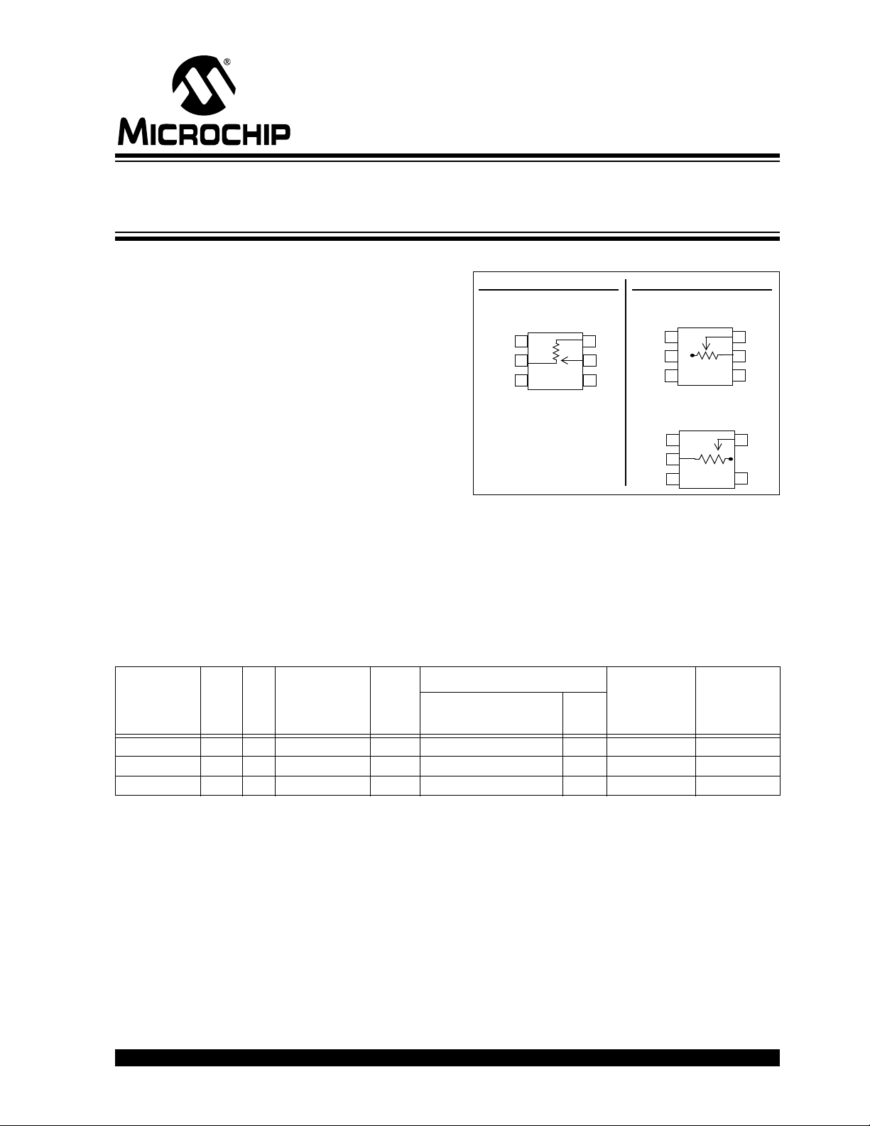
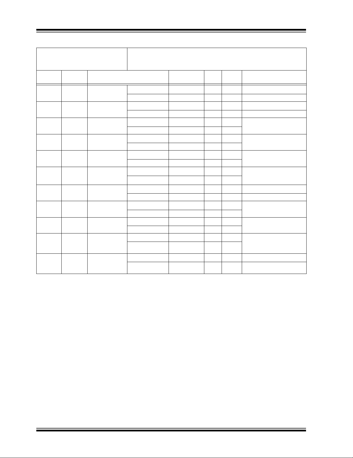
MCP4017/18/19
MCP4018
SC70-6
MCP4019
SC70-5
Rheostat
4
1
2
3
5
W
SDA
V
DD
V
SS
SCL
4
1
2
3
6
A
SDA
V
DD
V
SS
SCL
5
W
A
W
W
A
B
B
Potentiometer
MCP4017
SC70-6
4
1
2
3
6
W
SDA
V
DD
V
SS
SCL
5
B
A
W
B
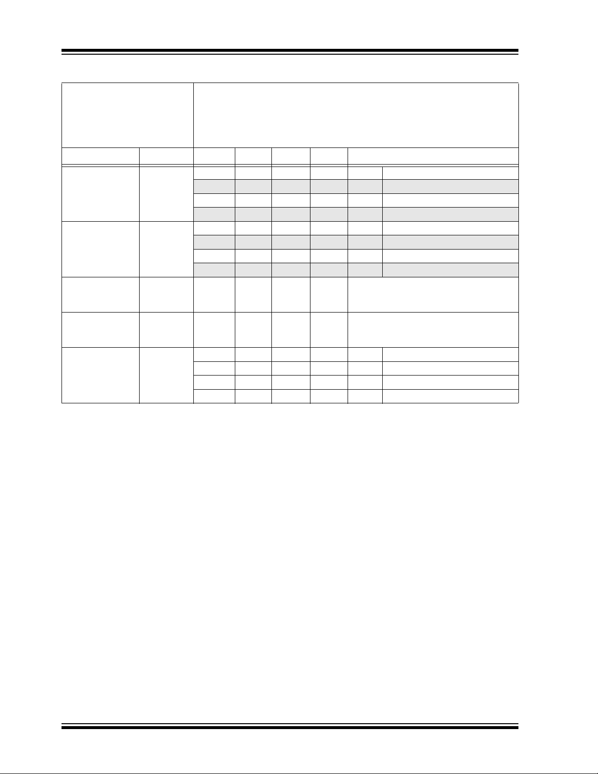
7-Bit Single I2C™ Digital POT with Volatile Memory in
SC70
Features
• Potentiometer or Rheostat configuration options
• 7-bit: Resistor Network Resolution
- 127 Resistors (128 Steps)
• Zero Scale to Full Scale Wiper operation
Resistances: 5 kΩ, 10 kΩ, 50 kΩ, or 100 kΩ
•R
AB
• Low Wiper Resistance: 100Ω (typical)
• Low Tempco:
- Absolute (Rheostat): 50 ppm typical
(0°C to 70°C)
- Ratiometric (Potentiometer): 10 ppm typical
2
•Simple I
C Protocol with read & write commands
• Brown-out reset protection (1.5V typical)
• Power-on Default Wiper Setting (Mid-scale)
• Low-Power Operation:
- 2.5 µA Static Current (typical)
• Wide Operating Voltage Range:
- 2.7V to 5.5V - Device Characteristics
Specified
- 1.8V to 5.5V - Device Operation
Device Features
Package Types
• Wide Bandwidth (-3 dB) Operation:
- 2 MHz (typical) for 5.0 kΩ device
• Extended temperature range (-40°C to +125°C)
• Very small package (SC70)
• Lead free (Pb-free) package
Resistance (typical)
VDD
Device
Control
Interface
Wiper
Configuration
# of Steps
Memory
Type
Wiper
(Ω)
Operating
Range
(1)
PackageOptions (kΩ)
MCP4017 I2C 128 Rheostat RAM 5.0, 10.0, 50.0, 100.0 75 1.8V to 5.5V SC70-6
MCP4018 I
2
C 128 Potentiometer RAM 5.0, 10.0, 50.0, 100.0 75 1.8V to 5.5V SC70-6
MCP4019 I2C 128 Rheostat RAM 5.0, 10.0, 50.0, 100.0 75 1.8V to 5.5V SC70-5
Note 1: Analog characteristics only tested from 2.7V to 5.5V
© 2009 Microchip Technology Inc. DS22147A-page 1
MCP4017/18/19
Power-up/
Brown-out
Control
VDD
V
SS
I2C Serial
Interface
Module,
Control
Logic, &
Resistor
Network 0
(Pot 0)
SCL
SDA
A
(2)
W
B
(1, 2)
Note 1
Note 1: Some configurations will have this
signal internally connected to ground.
2: In some configurations, this signal
may not be connected externally
Memory
(internally floating or grounded).
Device Block Diagram
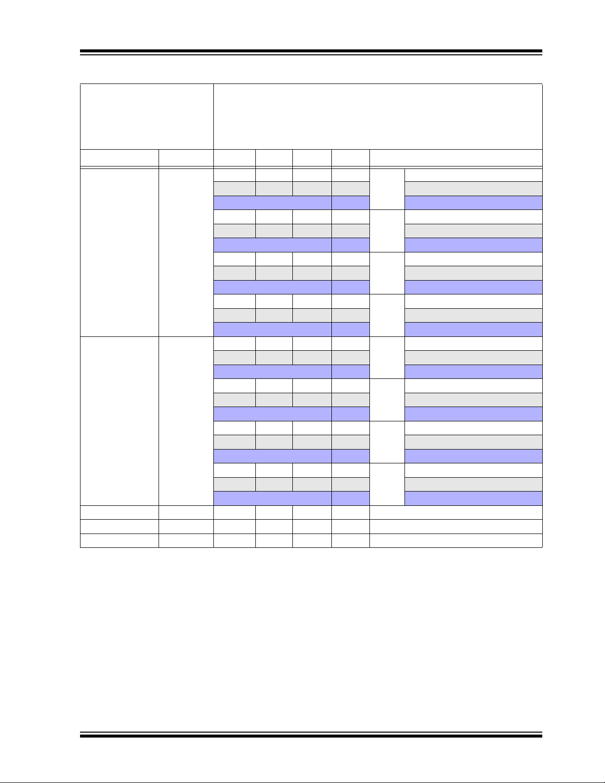
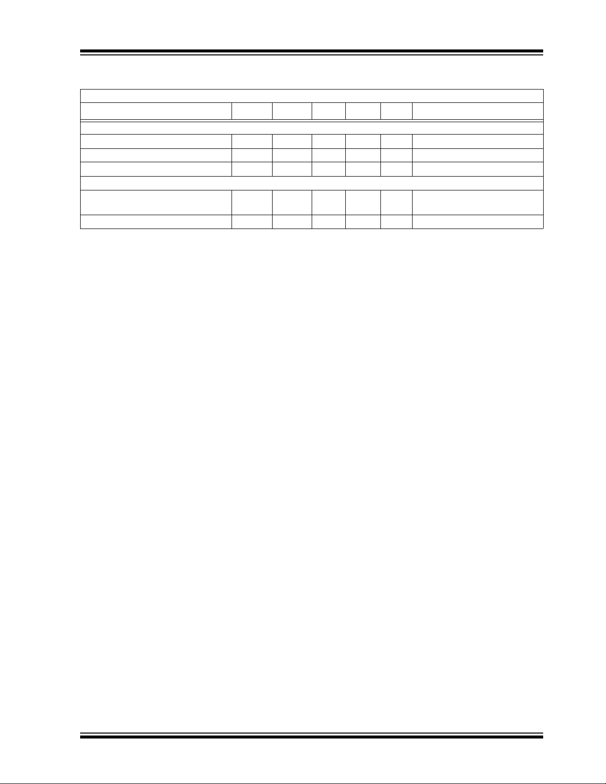
Comparison of Similar Microchip Devices
Wiper
Device
MCP4017 I2C 128 Rheostat RAM 5.0, 10.0, 50.0, 100.0 1.8V to 5.5V No No SC70-6
MCP4012 U/D 64 Rheostat RAM 2.1, 5.0, 10.0, 50.0 1.8V to 5.5V Yes No SOT-23-6
MCP4022 U/D 64 Rheostat EE 2.1, 5.0, 10.0, 50.0 2.7V to 5.5V Yes Ye s SOT-23-6
MCP4132 SPI 129 Rheostat RAM 5.0, 10.0, 50.0, 100.0 1.8V to 5.5V Ye s No PDIP-8,
MCP4142 SPI 129 Rheostat EE 5.0, 10.0, 50.0, 100.0 2.7V to 5.5V Yes Ye s
MCP4152 SPI 257 Rheostat RAM 5.0, 10.0, 50.0, 100.0 1.8V to 5.5V Ye s No
MCP4162 SPI 257 Rheostat EE 5.0, 10.0, 50.0, 100.0 2.7V to 5.5V Yes Ye s
MCP4532 I2C 129 Rheostat RAM 5.0, 10.0, 50.0, 100.0 1.8V to 5.5V Yes No MSOP-8,
MCP4542 I2C 129 Rheostat EE 5.0, 10.0, 50.0, 100.0 2.7V to 5.5V Yes Yes
MCP4552 I2C 257 Rheostat RAM 5.0, 10.0, 50.0, 100.0 1.8V to 5.5V Yes No
MCP4562 I2C 257 Rheostat EE 5.0, 10.0, 50.0, 100.0 2.7V to 5.5V Yes Yes
MCP4018 I
MCP4013 U/D 64 Potentiometer RAM 2.1, 5.0, 10.0, 50.0 1.8V to 5.5V Yes No SOT-23-6
MCP4023 U/D 64 Potentiometer EE 2.1, 5.0, 10.0, 50.0 2.7V to 5.5V Yes Yes SOT-23-6
MCP4019 I
MCP4014 U/D 64 Rheostat RAM 2.1, 5.0, 10.0, 50.0 1.8V to 5.5V Yes No SOT-23-5
MCP4024 U/D 64 Rheostat EE 2.1, 5.0, 10.0, 50.0 2.7V to 5.5V Yes Yes SOT-23-5
Note 1: This table is broken into three groups by a thick line (and color coding). The unshaded devices in this table
2: Analog characteristics only tested from 2.7V to 5.5V
DS22147A-page 2 © 2009 Microchip Technology Inc.
Control
Interface
2
C 128 Potentiometer RAM 5.0, 10.0, 50.0, 100.0 1.8V to 5.5V No No SC70-6
2
C 128 Rheostat RAM 5.0, 10.0, 50.0, 100.0 1.8V to 5.5V No No SC70-5
are the devices described in this data sheet, while the shaded devices offer a comparable resistor network
configuration.
Configuration
# of Steps
Memory
(1)
Resistance (typical)
VDD
Operating
Type
Range
(2)
HV
Interface
WiperLock
Technology
PackageOptions (kΩ)
SOIC-8,
MSOP-8,
DFN-8
DFN-8

MCP4017/18/19
1.0 ELECTRICAL CHARACTERISTICS
Absolute Maximum Ratings †
Voltage on VDD with respect to VSS..... -0.6V to +7.0V
Voltage on SCL, and SDA with respect to VSS
.............................................................................
Voltage on all other pins (A, W, and B)
with respect to V
Input clamp current, IIK
(VI < 0, VI > VDD, VI > VPP ON HV pins) ...........±20 mA
Output clamp current, I
(VO < 0 or VO > VDD) .......................................±20 mA
Maximum output current sunk by any Output pin
...........................................................................25 mA
Maximum output current sourced by any Output pin
...........................................................................25 mA
Maximum current out of V
Maximum current into VDD pin .........................100 mA
Maximum current into A, W and B pins........... ±2.5 mA
Package power dissipation (T
SC70-5............................................................302 mW
SC70-6.................................................................. TBD
Storage temperature ..........................-65°C to +150°C
Ambient temperature with power applied
...........................................................-40°C to +125°C
ESD protection on all pins ........................≥ 4 kV (HBM)
........................................................................≥ 400V (MM)
Maximum Junction Temperature (T
SS ............................
OK
pin ......................100 mA
SS
= +50°C, TJ = +150°C)
A
-0.6V to 12.5V
-0.3V to VDD + 0.3V
) .............. +150°C
J
† Notice: Stresses above those listed under “Maximum
Ratings” may cause permanent damage to the device.
This is a stress rating only and functional operation of
the device at those or any other conditions above those
indicated in the operational listings of this specification
is not implied. Exposure to maximum rating conditions
for extended periods may affect device reliability.
© 2009 Microchip Technology Inc. DS22147A-page 3
MCP4017/18/19
AC/DC CHARACTERISTICS
Standard Operating Conditions (unless otherwise specified)
Operating Temperature –40°C ≤ TA ≤ +125°C (extended)
DC Characteristics
Parameters Sym Min Typ Max Units Conditions
Supply Voltage V
Start Voltage
V
DD
V
DD
BOR
to ensure Wiper
Reset
Rise Rate to
V
DD
V
DDRR
ensure Power-on
Reset
Delay after device
T
BORD
exits the reset
state
> V
(V
DD
Supply Current
BOR
)
I
DD
(Note 8)
Note 1: Resistance is defined as the resistance between terminal A to terminal B.
2: INL and DNL are measured at V
3: MCP4018 device only, includes V
4: Resistor terminals A, W and B’s polarity with respect to each other is not restricted.
5: This specification by design.
6: Non-linearity is affected by wiper resistance (R
temperature.
7: POR/BOR is not rate dependent.
8: Supply current is independent of current through the resistor network
All parameters apply across the specified operating ranges unless noted.
= +2.7V to 5.5V, 5 kΩ, 10 kΩ, 50 kΩ, 100 kΩ devices.
V
DD
Typical specifications represent values for VDD = 5.5V, TA = +25°C.
2.7 — 5.5 V Analog Characteristics specified
1.8 — 5.5 V Digital Characteristics specified
— — 1.65 V RAM retention voltage (V
(Note 7)V/ms
—1020µS
— 45 80 µA Serial Interface Active,
Write all 0’s to Volatile Wiper
V
DD
= 5.5V, F
= 400 kHz
SCL
— 2.5 5 µA Serial Interface Inactive,
(Stop condition, SCL = SDA = V
Wiper = 0, VDD = 5.5V
with VA = VDD and VB = VSS.
W
WZSE
and V
.
WFSE
), which changes significantly over voltage and
W
RAM
) < V
IH
BOR
),
DS22147A-page 4 © 2009 Microchip Technology Inc.
MCP4017/18/19
AC/DC CHARACTERISTICS (CONTINUED)
Standard Operating Conditions (unless otherwise specified)
Operating Temperature –40°C ≤ T
DC Characteristics
All parameters apply across the specified operating ranges unless noted.
= +2.7V to 5.5V, 5 kΩ, 10 kΩ, 50 kΩ, 100 kΩ devices.
V
DD
Typical specifications represent values for V
Parameters Sym Min Typ Max Units Conditions
Resistance
(± 20%)
R
AB
4.0 5 6.0 kΩ -502 devices (Note 1)
8.0 10 12.0 kΩ -103 devices (Note 1)
40.0 50 60.0 kΩ -503 devices (Note 1)
80.0 100 120.0 kΩ -104 devices (Note 1)
Resolution N 128 Taps No Missing Codes
Step Resistance R
—RAB /
S
— Ω Note 5
(127)
Wiper Resistance R
W
— 100 170 Ω VDD = 5.5 V, IW = 2.0 mA, code = 00h
— 155 325 Ω V
Nominal
Resistance
Te mp c o
Ratiometeric
ΔR
/ΔT — 50 — ppm/°C TA = -20°C to +70°C
AB
— 100 — ppm/°C T
— 150 — ppm/°C T
/ΔT — 15 — ppm/°C Code = Midscale (3Fh)
ΔV
WB
Te mp c o
Resistor Terminal
V
A,VW,VB
Vss — V
DD
V Note 4, Note 5
Input Voltage
Range (Terminals
A, B and W)
Maximum current
through Terminal
(A, W or B)
Note 5
I
T
— — 2.5 mA Terminal A
— — 2.5 mA Terminal B
— — 2.5 mA Terminal W
— — 1.38 mA
— — 0.688 mA
— — 0.138 mA
— — 0.069 mA
Note 1: Resistance is defined as the resistance between terminal A to terminal B.
2: INL and DNL are measured at V
3: MCP4018 device only, includes V
with VA = VDD and VB = VSS.
W
WZSE
and V
WFSE
.
4: Resistor terminals A, W and B’s polarity with respect to each other is not restricted.
5: This specification by design.
6: Non-linearity is affected by wiper resistance (R
), which changes significantly over voltage and
W
temperature.
7: POR/BOR is not rate dependent.
8: Supply current is independent of current through the resistor network
≤ +125°C (extended)
A
= 5.5V, TA = +25°C.
DD
= 2.7 V, IW = 2.0 mA, code = 00h
DD
= -40°C to +85°C
A
= -40°C to +125°C
A
Terminal A
and
Terminal B
IAW, W = Full Scale (FS)
IBW, W = Zero Scale (ZS)
IAW or IBW, W = FS or ZS
IAB, VB = 0V, VA = 5.5V,
R
IAB, VB = 0V, VA = 5.5V,
R
IAB, VB = 0V, VA = 5.5V,
R
IAB, VB = 0V, VA = 5.5V,
R
AB(MIN)
AB(MIN)
AB(MIN)
AB(MIN)
= 4000
= 8000
= 40000
= 80000
© 2009 Microchip Technology Inc. DS22147A-page 5
MCP4017/18/19
AC/DC CHARACTERISTICS (CONTINUED)
Standard Operating Conditions (unless otherwise specified)
Operating Temperature –40°C ≤ T
DC Characteristics
All parameters apply across the specified operating ranges unless noted.
= +2.7V to 5.5V, 5 kΩ, 10 kΩ, 50 kΩ, 100 kΩ devices.
V
DD
Typical specifications represent values for V
Parameters Sym Min Typ Max Units Conditions
Full Scale Error
(MCP4018 only)
(code = 7Fh)
V
WFSE
-3.0 -0.1 — LSb 5 kΩ 2.7V ≤ VDD ≤ 5.5V
-2.0 -0.1 — LSb 10 kΩ 2.7V ≤ VDD ≤ 5.5V
-0.5 -0.1 — LSb 50 kΩ 2.7V ≤ V
-0.5 -0.1 — LSb 100 kΩ 2.7V ≤ VDD ≤ 5.5V
Zero Scale Error
(MCP4018 only)
(code = 00h)
V
WZSE
— +0.1 +3.0 LSb 5 kΩ 2.7V ≤ VDD ≤ 5.5V
— +0.1 +2.0 LSb 10 kΩ 2.7V ≤ VDD ≤ 5.5V
— +0.1 +0.5 LSb 50 kΩ 2.7V ≤ V
— +0.1 +0.5 LSb 100 kΩ 2.7V ≤ VDD ≤ 5.5V
Potentiometer
INL -0.5 ±0.25 +0.5 LSb 2.7V ≤ V
Integral
Non-linearity
Potentiometer
DNL -0.25 ±0.125 +0.25 LSb 2.7V ≤ V
Differential Nonlinearity
Bandwidth -3 dB
(See Figure 2-83,
load = 30 pF)
BW — 2 — MHz 5 kΩ Code = 3Fh
—1—MHz10kΩ Code = 3Fh
— 260 — kHz 50 kΩ Code = 3Fh
— 100 — kHz 100 kΩ Code = 3Fh
Note 1: Resistance is defined as the resistance between terminal A to terminal B.
2: INL and DNL are measured at V
3: MCP4018 device only, includes V
with VA = VDD and VB = VSS.
W
WZSE
and V
WFSE
.
4: Resistor terminals A, W and B’s polarity with respect to each other is not restricted.
5: This specification by design.
6: Non-linearity is affected by wiper resistance (R
), which changes significantly over voltage and
W
temperature.
7: POR/BOR is not rate dependent.
8: Supply current is independent of current through the resistor network
≤ +125°C (extended)
A
= 5.5V, TA = +25°C.
DD
≤ 5.5V
DD
MCP4018 device only (Note 2)
≤ 5.5V
DD
MCP4018 device only (Note 2)
DD
DD
≤ 5.5V
≤ 5.5V
DS22147A-page 6 © 2009 Microchip Technology Inc.
MCP4017/18/19
AC/DC CHARACTERISTICS (CONTINUED)
Standard Operating Conditions (unless otherwise specified)
Operating Temperature –40°C ≤ T
DC Characteristics
All parameters apply across the specified operating ranges unless noted.
= +2.7V to 5.5V, 5 kΩ, 10 kΩ, 50 kΩ, 100 kΩ devices.
V
DD
Typical specifications represent values for V
Parameters Sym Min Typ Max Units Conditions
Rheostat Integral
Non-linearity
MCP4018
(Note 3)
MCP4017 and
MCP4019 devices
only (Note 3)
R-INL -2.0 ±0.5 +2.0 LSb 5 kΩ 5.5V, I
-5.0 +3.5 +5.0 LSb 2.7V, IW = 430 µA (Note 6)
See Section 2.0 LSb 1.8V (Note 6)
-2.0 ±0.5 +2.0 LSb 10 kΩ 5.5V, IW = 450 µA
-4.0 +2.5 +4.0 LSb 2.7V, IW = 215 µA (Note 6)
See Section 2.0 LSb 1.8V (Note 6)
-1.125 ±0.5 +1.125 LSb 50 kΩ 5.5V, I
-1.5 +1 +1.5 LSb 2.7V, IW = 43 µA (Note 6)
See Section 2.0 LSb 1.8V (Note 6)
-0.8 ±0.5 +0.8 LSb 100 kΩ 5.5V, IW = 45 µA
-1.125 +0.25 +1.125 LSb 2.7V, IW = 21.5 µA (Note 6)
See Section 2.0 LSb 1.8V (Note 6)
Rheostat
Differential Nonlinearity
MCP4018
(Note 3)
MCP4017 and
MCP4019 devices
only (Note 3)
R-DNL -0.5 ±0.25 +0.5 LSb 5 kΩ 5.5V, I
-0.75 +0.5 +0.75 LSb 2.7V, IW = 430 µA (Note 6)
See Section 2.0 LSb 1.8V (Note 6)
-0.5 ±0.25 +0.5 LSb 10 kΩ 5.5V, IW = 450 µA
-0.75 +0.5 +0.75 LSb 2.7V, IW = 215 µA (Note 6)
See Section 2.0 LSb 1.8V (Note 6)
-0.375 ±0.25 +0.375 LSb 50 kΩ 5.5V, IW = 90 µA
-0.375 ±0.25 +0.375 LSb 2.7V, IW = 43 µA (Note 6)
See Section 2.0 LSb 1.8V (Note 6)
-0.375 ±0.25 +0.375 LSb 100 kΩ 5.5V, I
-0.375 ±0.25 +0.375 LSb 2.7V, IW = 21.5 µA (Note 6)
See Section 2.0 LSb 1.8V (Note 6)
Capacitance (PA)C
Capacitance (P
)CW— 120 — pF f =1 MHz, Code = Full Scale
w
Capacitance (PB)C
AW
BW
— 75 — pF f =1 MHz, Code = Full Scale
— 75 — pF f =1 MHz, Code = Full Scale
Note 1: Resistance is defined as the resistance between terminal A to terminal B.
2: INL and DNL are measured at V
3: MCP4018 device only, includes V
with VA = VDD and VB = VSS.
W
WZSE
and V
WFSE
.
4: Resistor terminals A, W and B’s polarity with respect to each other is not restricted.
5: This specification by design.
6: Non-linearity is affected by wiper resistance (R
), which changes significantly over voltage and
W
temperature.
7: POR/BOR is not rate dependent.
8: Supply current is independent of current through the resistor network
≤ +125°C (extended)
A
= 5.5V, TA = +25°C.
DD
= 900 µA
W
= 90 µA
W
= 900 mA
W
= 45 µA
W
© 2009 Microchip Technology Inc. DS22147A-page 7
MCP4017/18/19
AC/DC CHARACTERISTICS (CONTINUED)
Standard Operating Conditions (unless otherwise specified)
Operating Temperature –40°C ≤ T
DC Characteristics
All parameters apply across the specified operating ranges unless noted.
= +2.7V to 5.5V, 5 kΩ, 10 kΩ, 50 kΩ, 100 kΩ devices.
V
DD
Typical specifications represent values for V
Parameters Sym Min Typ Max Units Conditions
Digital Inputs/Outputs (SDA, SCK)
Schmitt Trigger
V
IH
0.7 V
DD
—— V1.8V ≤ VDD ≤ 5.5V
High Input
Threshold
Schmitt Trigger
V
IL
-0.5 — 0.3V
DD
V
Low Input
Threshold
Hysteresis of
Schmitt Trigger
Inputs (Note 5)
Output Low
Voltage (SDA)
Input Leakage
V
HYS
VOL V
I
IL
—0.1VDD— V All inputs except SDA and SCL
N.A. — — V
N.A. — — V V
0.1 V
0.05 V
SS
V
SS
DD
—— V
—— V VDD ≥ 2.0V
DD
—0.2VDD VVDD < 2.0V, IOL = 1 mA
—0.4 VVDD ≥ 2.0V, IOL = 3 mA
-1 — 1 µA VIN = VDD and VIN = VSS
Current
Pin Capacitance C
, C
IN
OUT
—10—pFf
RAM (Wiper) Value
Value Range N 0h — 7Fh hex
Wiper POR/BOR
N
POR/BOR
3Fh hex
Val ue
Power Requirements
Power Supply
PSS — 0.0005 0.0035 %/% V
Sensitivity
(MCP4018 only)
Note 1: Resistance is defined as the resistance between terminal A to terminal B.
2: INL and DNL are measured at V
3: MCP4018 device only, includes V
with VA = VDD and VB = VSS.
W
WZSE
and V
WFSE
.
4: Resistor terminals A, W and B’s polarity with respect to each other is not restricted.
5: This specification by design.
6: Non-linearity is affected by wiper resistance (R
), which changes significantly over voltage and
W
temperature.
7: POR/BOR is not rate dependent.
8: Supply current is independent of current through the resistor network
≤ +125°C (extended)
A
= 5.5V, TA = +25°C.
DD
SDA
100 kHz
and
SCL
400 kHz
= 400 kHz
C
= 2.7V to 5.5V,
DD
VA = 2.7V, Code = 3Fh
V
< 2.0V
DD
≥ 2.0V
DD
VDD < 2.0V
DS22147A-page 8 © 2009 Microchip Technology Inc.
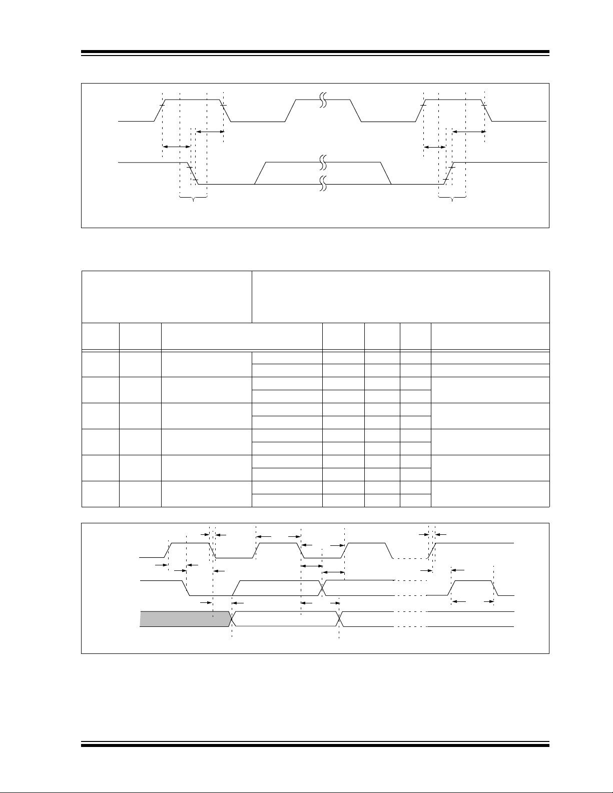
1.1 I2C Mode Timing Waveforms and Requirements
91
93
SCL
SDA
START
Condition
STOP
Condition
90
92
Note 1: Refer to specification D102 (Cb) for load conditions.
90
91 92
100
101
103
106
107
109
109
110
102
SCL
SDA
In
SDA
Out
FIGURE 1-1: I2C Bus Start/Stop Bits Timing Waveforms.
MCP4017/18/19
TABLE 1-1: I
I2C AC Characteristics
Param.
No.
D102 Cb Bus capacitive
Symbol Characteristic Min Max Units Conditions
90 T
91 T
92 T
93 T
2
C BUS START/STOP BITS REQUIREMENTS
Standard Mode 0 100 kHz Cb = 400 pF, 1.8V - 5.5V
F
SCL
loading
SU:STA START condition 100 kHz mode 4700 — ns Only relevant for repeated
Setup time 400 kHz mode 600 — ns
HD:STA START condition 100 kHz mode 4000 — ns After this period the first
Hold time 400 kHz mode 600 — ns
SU:STO STOP condition 100 kHz mode 4000 — ns
Setup time 400 kHz mode 600 — ns
HD:STO STOP condition 100 kHz mode 4000 — ns
Hold time 400 kHz mode 600 — ns
Standard Operating Conditions (unless otherwise specified)
Operating Temperature –40°C ≤ T
Operating Voltage VDD range is described in Section 2.0 “Typical
Performance Curves”
Fast Mode 0 400 kHz Cb = 400 pF, 2.7V - 5.5V
100 kHz mode — 400 pF
400 kHz mode — 400 pF
A ≤ +125°C (Extended)
START condition
clock pulse is generated
FIGURE 1-2: I2C Bus Data Timing.
© 2009 Microchip Technology Inc. DS22147A-page 9
MCP4017/18/19
TABLE 1-2: I2C BUS DATA REQUIREMENTS (SLAVE MODE)
I2C AC Characteristics
Parame-
Sym Characteristic Min Max Units Conditions
ter No.
100 T
101 T
(5)
102A
(5)
102B
(5)
103A
(5)
103B
HIGH
LOW
T
RSCL
T
RSDA
T
FSCL
T
FSDA
Clock high time 100 kHz mode 4000 — ns 1.8V-5.5V
Clock low time 100 kHz mode 4700 — ns
SCL rise time 100 kHz mode — 1000 ns Cb is specified to be from
SDA rise time 100 kHz mode — 1000 ns Cb is specified to be from
SCL fall time 100 kHz mode — 300 ns Cb is specified to be from
SDA fall time 100 kHz mode — 300 ns Cb is specified to be from
106 THD:DAT Data input hold
time
107 T
SU:DAT Data input
setup time
109 T
AA
Output valid
from clock
110 T
T
Bus free time 100 kHz mode 4700 — ns Time the bus must be free
BUF
Input filter spike
SP
suppression
(SDA and SCL)
Note 1: As a transmitter, the device must provide this internal minimum delay time to bridge the undefined region
(min. 300 ns) of the falling edge of SCL to avoid unintended generation of START or STOP conditions.
2: A fast-mode (400 kHz) I
requirement tsu; DAT ≥ 250 ns must then be met. This will automatically be the case if the device does not
stretch the LOW period of the SCL signal. If such a device does stretch the LOW period of the SCL signal, it
must output the next data bit to the SDA line
R max.+tsu;DAT = 1000 + 250 = 1250 ns (according to the standard-mode I
T
the SCL line is released.
3: The MCP4018/MCP4019 device must provide a data hold time to bridge the undefined part between V
and VIL of the falling edge of the SCL signal. This specification is not a part of the I2C specification, but must
be tested in order to guarantee that the output data will meet the setup and hold specifications for the receiving device.
4: Use Cb in pF for the calculations.
5: Not Tested.
6: A Master Transmitter must provide a delay to ensure that difference between SDA and SCL fall times do not
unintentionally create a Start or Stop condition.
Standard Operating Conditions (unless otherwise specified)
Operating Temperature –40°C ≤ TA ≤ +125°C (Extended)
Operating Voltage VDD range is described in AC/DC characteristics
400 kHz mode 600 — ns 2.7V-5.5V
1.8V-5.5V
400 kHz mode 1300 — ns 2.7V-5.5V
400 kHz mode 20 + 0.1Cb 300 ns
400 kHz mode 20 + 0.1Cb 300 ns
400 kHz mode 20 + 0.1Cb 40 ns
400 kHz mode
20 + 0.1Cb
(4)
300 ns
100 kHz mode 0 — ns
10 to 400 pF
10 to 400 pF
10 to 400 pF
10 to 400 pF
1.8V-5.5V, Note 6
400 kHz mode 0 — ns 2.7V-5.5V, Note 6
100 kHz mode 250 — ns
(2)
400 kHz mode 100 — ns
100 kHz mode — 3450 ns
(1)
400 kHz mode — 900 ns
400 kHz mode 1300 — ns
before a new transmission
can start
100 kHz mode — 50 ns Philips Spec states N.A.
400 kHz mode — 50 ns
2
C-bus device can be used in a standard-mode (100 kHz) I2C-bus system, but the
2
C bus specification) before
IH
DS22147A-page 10 © 2009 Microchip Technology Inc.
MCP4017/18/19
TEMPERATURE CHARACTERISTICS
Electrical Specifications: Unless otherwise indicated, VDD= +1.8V to +5.5V, VSS=GND.
Parameters Sym Min Typ Max Units Conditions
Temperature Ranges
Specified Temperature Range T
Operating Temperature Range T
Storage Temperature Range T
Thermal Package Resistances
Thermal Resistance, 5L-SC70
(Note 1)
Thermal Resistance, 6L-SC70 θ
Note 1: Package Power Dissipation (PDIS) is calculated as follows:
P
= (TJ - TA) / θJA,
DIS
where: TJ = Junction Temperature, TA = Ambient Temperature.
A
A
A
θ
JA
JA
-40 — +125 °C
-40 — +125 °C
-65 — +150 °C
—331—°C/W
—TBD—°C/W
© 2009 Microchip Technology Inc. DS22147A-page 11

MCP4017/18/19
NOTES:
DS22147A-page 12 © 2009 Microchip Technology Inc.
MCP4017/18/19
0
10
20
30
40
50
60
-40 0 40 80 120
Temperature (°C)
I
DD
(µA)
100 kHz, 5.5V
400 kHz, 5.5V
100 kHz, 2.7V
400 kHz, 2.7V
0
0.2
0.4
0.6
0.8
1
1.2
1.4
1.6
1.8
2
-40 0 40 80 120
Temperature (°C)
I
DD
Interface Inactive (µA)
5.5V
2.7V
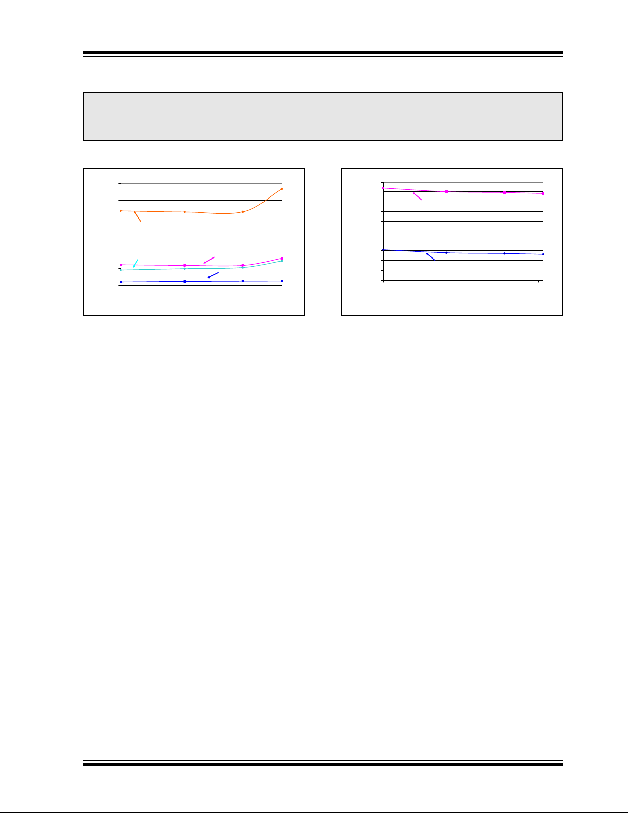
2.0 TYPICAL PERFORMANCE CURVES
Note: The graphs and tables provided following this note are a statistical summary based on a limited number of
samples and are provided for informational purposes only. The performance characteristics listed herein
are not tested or guaranteed. In some graphs or tables, the data presented may be outside the specified
operating range (e.g., outside specified power supply range) and therefore outside the warranted range.
Note: Unless otherwise indicated, TA = +25°C, VDD = 5V, VSS = 0V.
FIGURE 2-1: Interface Active Current
(I
) vs. SCL Frequency (f
DD
(V
= 1.8V, 2.7V and 5.5V).
DD
) and Temperature
SCL
FIGURE 2-2: Interface Inactive Current
) vs. Temperature and VDD.
(I
SHDN
(V
= 1.8V, 2.7V and 5.5V).
DD
© 2009 Microchip Technology Inc. DS22147A-page 13
MCP4017/18/19
20
40
60
80
100
120
0 326496
Wiper Setting (decimal)
Wiper Resistance (R
W
(ohms)
-0.3
-0.2
-0.1
0
0.1
0.2
0.3
Error (LSb)
-40C Rw 25C Rw 85C Rw 125C Rw
-40C INL 25C INL 85C INL 125C INL
-40C DNL 25C DNL 85C DNL 125C DNL
INL
DNL
R
W
-40°C
25°C
85°C
125°C
20
60
100
140
180
220
260
300
0326496
Wiper Setting (decimal)
Wiper Resistance (R
W
(ohms)
-0.3
-0.2
-0.1
0
0.1
0.2
0.3
Error (LSb)
-40C Rw 25C Rw 85C Rw 125C Rw
-40C INL 25C INL 85C INL 125C I NL
-40C DNL 25C DNL 85C DNL 125C DNL
INL
DNL-40°C
25°C
85°
R
W
125°C
Note: Refer to AN1080 for additional informa-
tion on the characteristics of the wiper
resistance (R
W
) with respect to device
voltage and wiper setting value.
0
500
1000
1500
2000
2500
0 326496
Wiper Setting (decimal)
Wiper Resistance (R
W
(ohms)
-0.35
-0.25
-0.15
-0.05
0.05
0.15
0.25
0.35
Error (LSb)
-40C Rw 25C Rw 85C Rw 125C Rw
-40C INL 25C INL 85C INL 125C I NL
-40C DNL 25C DNL 85C DNL 125C DNL
INL DNL
RW
20
40
60
80
100
120
0 326496
Wiper Setting (decimal)
Wiper Resistance (R
W
(ohms)
-0.3
-0.2
-0.1
0
0.1
0.2
0.3
Error (LSb)
-40C Rw 25C Rw 85C Rw 125C Rw
-40C INL 25C INL 85C INL 125C INL
-40C DNL 25C DNL 85C DNL 125C DNL
INL
DNLR
-40°C
25°C
85°C 125°C
20
60
100
140
180
220
260
300
0326496
Wiper Setting (decimal)
Wiper Resistance (R
W
(ohms)
-1
0
1
2
3
Error (LSb)
-40C Rw 25C Rw 85C Rw 125C Rw
-40C INL 25C INL 85C INL 125C INL
-40C DNL 25C DNL 85C DNL 125C DNL
INL
DNL
R
W
-40°C
25°C
85°C
125°C
Note: Refer to AN1080 for additional informa-
tion on the characteristics of the wiper
resistance (R
W
) with respect to device
voltage and wiper setting value.
0
500
1000
1500
2000
2500
0326496
Wiper Setting (decimal)
Wiper Resistance (R
W
(ohms)
-1
4
9
14
19
24
29
34
39
44
Error (LSb)
-40C Rw 25C Rw 85C Rw 125C Rw
-40C INL 25C INL 85C INL 125C INL
-40C DNL 25C DNL 85C DNL 125C DNL
INL
DNL
RW
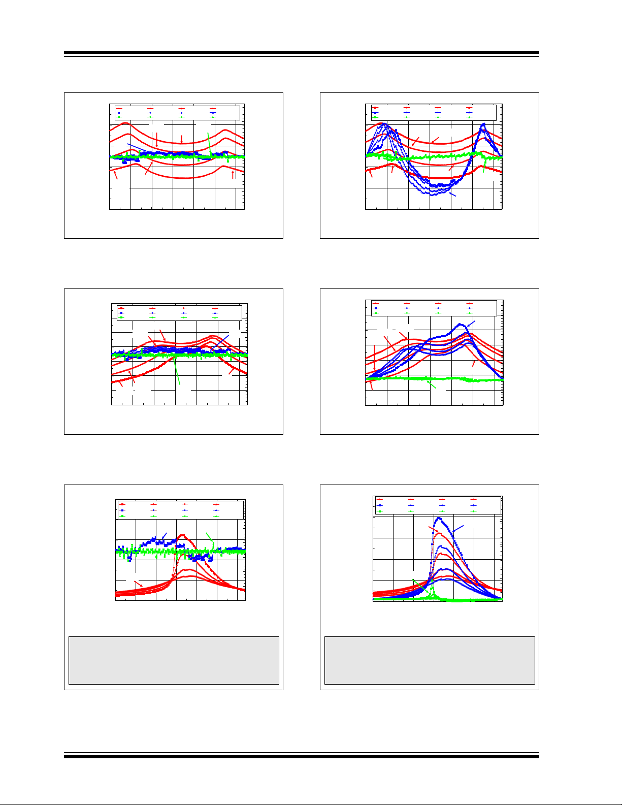
Note: Unless otherwise indicated, TA = +25°C, VDD = 5V, VSS = 0V.
)
FIGURE 2-3: 5.0 kΩ : Pot Mode – RW (Ω),
INL (LSb), DNL (LSb) vs. Wiper Setting and
Temperature (V
)
= 5.5V). (A = VDD, B = VSS).
DD
)
W
FIGURE 2-6: 5.0 k
(
Ω
), INL (LSb), DNL (LSb) vs. Wiper Setting and
Temperature (V
)
= 5.5V).(IW = 1.4mA, B = VSS)
DD
Ω
: Rheo Mode – RW
Ω
FIGURE 2-4: 5.0 k
: Pot Mode – RW (Ω),
INL (LSb), DNL (LSb) vs. Wiper Setting and
Temperature (V
)
FIGURE 2-5: 5.0 k
INL (LSb), DNL (LSb) vs. Wiper Setting and
Temperature (V
DS22147A-page 14 © 2009 Microchip Technology Inc.
= 2.7V). (A = VDD, B = VSS)
DD
= 1.8V). (A = VDD, B = VSS)
DD
Ω
: Pot Mode – RW (Ω),
Ω
FIGURE 2-7: 5.0 k
(
Ω
), INL (LSb), DNL (LSb) vs. Wiper Setting and
Temperature (V
)
= 2.7V).(IW = 450uA, B = VSS)
DD
FIGURE 2-8: 5.0 k
(
Ω
), INL (LSb), DNL (LSb) vs. Wiper Setting and
Temperature (V
= 1.8V). (IW = TBD, B = VSS)
DD
: Rheo Mode – RW
Ω
: Rheo Mode – RW
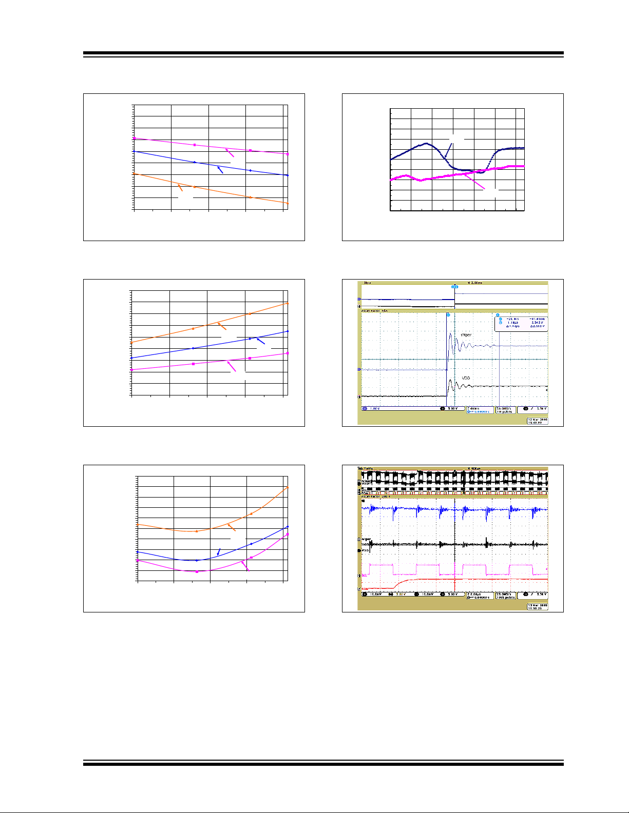
Note: Unless otherwise indicated, TA = +25°C, VDD = 5V, VSS = 0V.
-1.8
-1.6
-1.4
-1.2
-1.0
-0.8
-0.6
-0.4
-0.2
0.0
-40 0 40 80 120
Ambient Temperature (°C)
Full-Scale Error (FSE) (LSb)
2.7
5.5V
1.8V
0.0
0.2
0.4
0.6
0.8
1.0
1.2
1.4
1.6
1.8
-40 0 40 80 120
Ambient Temperature (°C)
Zero-Scale Error (ZSE) (LSb)
2.7
5.5V
1.8V
5000
5020
5040
5060
5080
5100
5120
5140
5160
5180
5200
-40 0 40 80 120
Ambient Temperature (°C)
Nominal Resistance (R
AB
(Ohms)
2.7V
5.5V
1.8V
0
20
40
60
80
100
120
140
160
180
200
0 326496
Wiper Setting (decimal)
R
BW
Tempco (PPM)
2.7V
5.5V
Wiper
V
DD
MCP4017/18/19
FIGURE 2-9: 5.0 kΩ : Full Scale Error
(FSE) vs. Temperature (V
FIGURE 2-10: 5.0 k
(ZSE) vs. Temperature (V
)
= 5.5V, 2.7V, 1.8V).
DD
Ω
: Zero Scale Error
= 5.5V, 2.7V, 1.8V).
DD
FIGURE 2-12: 5.0 k
Δ
RWB / ΔT vs. Code.
FIGURE 2-13: 5.0 k
Response Time.
Ω
: RBW Tempco
Ω
: Power-Up Wiper
FIGURE 2-11: 5.0 k
(
Ω
) vs. Temperature and VDD.
© 2009 Microchip Technology Inc. DS22147A-page 15
Ω
: Nominal Resistance
Ω
FIGURE 2-14: 5.0 k
: Digital Feedthrough
(SCL signal coupling to Wiper pin).
MCP4017/18/19
Note: Unless otherwise indicated, TA = +25°C, VDD = 5V, VSS = 0V.
FIGURE 2-15: 5.0 kΩ : Write Wiper (40h →
3Fh) Settling Time (V
FIGURE 2-16: 5.0 k
→
3Fh) Settling Time (VDD=2.7V).
=5.5V).
DD
Ω
: Write Wiper (40h
FIGURE 2-18: 5.0 k
00h) Settling Time (V
FIGURE 2-19: 5.0 k
00h) Settling Time (V
DD
DD
Ω
: Write Wiper (FFh →
=5.5V).
Ω
: Write Wiper (FFh →
=2.7V).
Ω
FIGURE 2-17: 5.0 k
3Fh) Settling Time (V
DS22147A-page 16 © 2009 Microchip Technology Inc.
: Write Wiper (40h →
=1.8V).
DD
FIGURE 2-20: 5.0 k
00h) Settling Time (V
Ω
: Write Wiper (FFh →
=1.8V).
DD
Note: Unless otherwise indicated, TA = +25°C, VDD = 5V, VSS = 0V.
20
40
60
80
100
120
0 326496
Wiper Setting (decimal)
Wiper Resistance (R
W
(ohms)
-0.3
-0.2
-0.1
0
0.1
0.2
0.3
Error (LSb)
-40C Rw 25C Rw 85C Rw 125C Rw
-40C INL 25C INL 85C INL 125C INL
-40C DNL 25C DNL 85C DNL 125C DNL
INL
DNL
R
W
-40°C
25°C
85°C
125°C
20
60
100
140
180
220
260
300
0326496
Wiper Setting (decimal)
Wiper Resistance (R
W
(ohms)
-0.3
-0.2
-0.1
0
0.1
0.2
0.3
Error (LSb)
-40C Rw 25C Rw 85C Rw 125C Rw
-40C INL 25C INL 85C INL 125C I NL
-40C DNL 25C DNL 85C DNL 125C DNL
INL
DNL
-40°C
25°C
85°
R
W
125°C
Note: Refer to AN1080 for additional informa-
tion on the characteristics of the wiper
resistance (R
W
) with respect to device
voltage and wiper setting value.
0
1000
2000
3000
0 326496
Wiper Setting (decimal)
Wiper Resistance (R
W
(ohms)
-0.35
-0.25
-0.15
-0.05
0.05
0.15
0.25
0.35
Error (LSb)
-40C Rw 25C Rw 85C Rw 125C Rw
-40C INL 25C INL 85C INL 125C I NL
-40C DNL 25C DNL 85C DNL 125C DNL
INL
DNL
RW
20
40
60
80
100
120
0 326496
Wiper Setting (decimal)
Wiper Resistance (R
W
(ohms)
-0.3
-0.2
-0.1
0
0.1
0.2
0.3
Error (LSb)
-40C Rw 25C Rw 85C Rw 125C Rw
-40C INL 25C INL 85C INL 125C INL
-40C DNL 25C DNL 85C DNL 125C DNL
INL
DNL
R
-40°C
25°C
85°C
125°C
20
60
100
140
180
220
260
300
0326496
Wiper Setting (decimal)
Wiper Resistance (R
W
(ohms)
-1
0
1
2
3
Error (LSb)
-40C Rw 25C Rw 85C Rw 125C Rw
-40C INL 25C INL 85C INL 125C INL
-40C DNL 25C DNL 85C DNL 125C DNL
INL
DNL
R
W
-40°C
25°C
85°C
125°C
Note: Refer to AN1080 for additional informa-
tion on the characteristics of the wiper
resistance (R
W
) with respect to device
voltage and wiper setting value.
0
1000
2000
3000
0326496
Wiper Setting (decimal)
Wiper Resistance (R
W
(ohms)
-1
4
9
14
19
24
29
34
39
Error (LSb)
-40C Rw 25C Rw 85C Rw 125C Rw
-40C INL 25C INL 85C INL 125C INL
-40C DNL 25C DNL 85C DNL 125C DNL
INL
DNLRW
MCP4017/18/19
)
FIGURE 2-21: 10 kΩ Pot Mode : RW (Ω),
INL (LSb), DNL (LSb) vs. Wiper Setting and
Temperature (V
)
= 5.5V). (A = VDD, B = VSS)
DD
)
W
FIGURE 2-24: 10 k
Ω
Rheo Mode : RW (Ω),
INL (LSb), DNL (LSb) vs. Wiper Setting and
Temperature (V
)
= 5.5V).(IW = 450uA, B = VSS)
DD
FIGURE 2-22: 10 k
Ω
INL (LSb), DNL (LSb) vs. Wiper Setting and
Temperature (V
)
FIGURE 2-23: 10 k
INL (LSb), DNL (LSb) vs. Wiper Setting and
Temperature (V
© 2009 Microchip Technology Inc. DS22147A-page 17
= 2.7V). (A = VDD, B = VSS)
DD
Ω
= 1.8V). (A = VDD, B = VSS)
DD
Pot Mode : RW (Ω),
Pot Mode : RW (Ω),
Ω
FIGURE 2-25: 10 k
Rheo Mode : RW (Ω),
INL (LSb), DNL (LSb) vs. Wiper Setting and
Temperature (V
)
FIGURE 2-26: 10 k
= 2.7V).(IW = 210uA, B = VSS)
DD
Ω
Rheo Mode : RW (Ω),
INL (LSb), DNL (LSb) vs. Wiper Setting and
Temperature (V
= 1.8V). (IW = TBD, B = VSS)
DD
MCP4017/18/19
-1.0
-0.9
-0.8
-0.7
-0.6
-0.5
-0.4
-0.3
-0.2
-0.1
0.0
-40 0 40 80 120
Ambient Temperature (°C)
Full-Scale Error (FSE) (LSb)
2.7
5.5V
1.8V
0.0
0.1
0.2
0.3
0.4
0.5
0.6
0.7
0.8
0.9
-40 0 40 80 120
Ambient Temperature (°C)
Zero-Scale Error (ZSE) (LSb)
2.7
5.5V
1.8V
9900
9950
10000
10050
10100
10150
10200
-40 0 40 80 120
Ambient Temperature (°C)
Nominal Resistance (R
AB
(Ohms)
2.7
5.5V
1.8V
0
20
40
60
80
100
0 326496
Wiper Setting (decimal)
R
BW
Tempco (PPM)
2.7V
5.5V
Wiper
V
DD
Note: Unless otherwise indicated, TA = +25°C, VDD = 5V, VSS = 0V.
FIGURE 2-27: 10 kΩ : Full Scale Error
(FSE) vs. Temperature (V
= 5.5V, 2.7V, 1.8V).
DD
FIGURE 2-30: 10 k
Δ
RWB / ΔT vs. Code.
Ω
: RBW Temp co
FIGURE 2-28: 10 k
(ZSE) vs. Temperature (V
)
FIGURE 2-29: 10 k
(
Ω
) vs. Temperature and VDD.
DS22147A-page 18 © 2009 Microchip Technology Inc.
Ω
: Zero Scale Error
= 5.5V, 2.7V, 1.8V).
DD
Ω
: Nominal Resistance
Ω
FIGURE 2-31: 10 k
: Power-Up Wiper
Response Time.
Ω
FIGURE 2-32: 10 k
: Digital Feedthrough
(SCL signal coupling to Wiper pin).
Note: Unless otherwise indicated, TA = +25°C, VDD = 5V, VSS = 0V.
MCP4017/18/19
FIGURE 2-33: 10 kΩ : Write Wiper (40h →
3Fh) Settling Time (V
FIGURE 2-34: 10 k
3Fh) Settling Time (V
=5.5V).
DD
Ω
: Write Wiper (40h →
=2.7V).
DD
FIGURE 2-36: 10 k
00h) Settling Time (V
FIGURE 2-37: 10 k
00h) Settling Time (V
DD
DD
Ω
: Write Wiper (FFh →
=5.5V).
Ω
: Write Wiper (FFh →
=2.7V).
Ω
FIGURE 2-35: 10 k
3Fh) Settling Time (V
© 2009 Microchip Technology Inc. DS22147A-page 19
: Write Wiper (40h →
=1.8V).
DD
FIGURE 2-38: 10 k
00h) Settling Time (V
Ω
: Write Wiper (FFh →
=1.8V).
DD
MCP4017/18/19
20
40
60
80
100
120
0 326496
Wiper Setting (decimal)
Wiper Resistance (R
W
(ohms)
-0.3
-0.2
-0.1
0
0.1
0.2
0.3
Error (LSb)
-40C Rw 25C Rw 85C Rw 125C Rw
-40C INL 25C INL 85C INL 125C INL
-40C DNL 25C DNL 85C DNL 125C DNL
INL
DNL
R
W
-40°C
25°C
85°C 125°C
20
60
100
140
180
220
260
300
0326496
Wiper Setting (decimal)
Wiper Resistance (R
W
(ohms)
-0.3
-0.2
-0.1
0
0.1
0.2
0.3
Error (LSb)
-40C Rw 25C Rw 85C Rw 125C Rw
-40C INL 25C INL 85C INL 125C I NL
-40C DNL 25C DNL 85C DNL 125C DNL
INL
DNL
-40°C
25°C
85°
R
W
125°C
Note: Refer to AN1080 for additional informa-
tion on the characteristics of the wiper
resistance (R
W
) with respect to device
voltage and wiper setting value.
0
2000
4000
6000
8000
10000
0326496
Wiper Setting (decimal)
Wiper Resistance (R
W
(ohms)
-0.35
-0.25
-0.15
-0.05
0.05
0.15
0.25
0.35
Error (LSb)
-40C Rw 25C Rw 85C Rw 125C Rw
-40C INL 25C INL 85C INL 125C INL
-40C DNL 25C DNL 85C DNL 125C DNL
INL
DNL
RW
20
40
60
80
100
120
0 326496
Wiper Setting (decimal)
Wiper Resistance (R
W
(ohms)
-0.3
-0.2
-0.1
0
0.1
0.2
0.3
Error (LSb)
-40C Rw 25C Rw 85C Rw 125C Rw
-40C INL 25C INL 85C INL 125C I NL
-40C DNL 25C DNL 85C DNL 125C DNL
INL
DNL
R
-40°C
25°C
85°C 125°C
20
60
100
140
180
220
260
300
0 326496
Wiper Setting (decimal)
Wiper Resistance (R
W
(ohms)
-0.3
-0.2
-0.1
0
0.1
0.2
0.3
Error (LSb)
-40C Rw 25C Rw 85C Rw 125C Rw
-40C INL 25C INL 85C INL 125C INL
-40C DNL 25C DNL 85C DNL 125C DNL
INL
DNL
R
W
-40°C
25°C
85°C
125°C
Note: Refer to AN1080 for additional informa-
tion on the characteristics of the wiper
resistance (R
W
) with respect to device
voltage and wiper setting value.
0
2000
4000
6000
8000
10000
0326496
Wiper Setting (decimal)
Wiper Resistance (R
W
(ohms)
-1
1
3
5
7
9
11
13
15
17
19
21
23
Error (LSb)
-40C Rw 25C Rw 85C Rw 125C Rw
-40C INL 25C INL 85C INL 125C INL
-40C DNL 25C DNL 85C DNL 125C DNL
INL
DNL
RW
Note: Unless otherwise indicated, TA = +25°C, VDD = 5V, VSS = 0V.
)
FIGURE 2-39: 50 kΩ Pot Mode : RW (Ω),
INL (LSb), DNL (LSb) vs. Wiper Setting and
Temperature (V
)
= 5.5V).
DD
)
W
FIGURE 2-42: 50 k
Ω
Rheo Mode : RW (Ω),
INL (LSb), DNL (LSb) vs. Wiper Setting and
Temperature (V
)
= 5.5V).(IW = 90uA, B = VSS)
DD
Ω
FIGURE 2-40: 50 k
Pot Mode : RW (Ω),
INL (LSb), DNL (LSb) vs. Wiper Setting and
Temperature (V
)
FIGURE 2-41: 50 k
INL (LSb), DNL (LSb) vs. Wiper Setting and
Temperature (V
DS22147A-page 20 © 2009 Microchip Technology Inc.
= 2.7V).
DD
= 1.8V).
DD
Ω
Pot Mode : RW (Ω),
Ω
FIGURE 2-43: 50 k
Rheo Mode : RW (Ω),
INL (LSb), DNL (LSb) vs. Wiper Setting and
Temperature (V
)
FIGURE 2-44: 50 k
= 2.7V).(IW = 45uA, B = VSS)
DD
Ω
Rheo Mode : RW (Ω),
INL (LSb), DNL (LSb) vs. Wiper Setting and
Temperature (V
= 1.8V). (IW = TBD, B = VSS)
DD

Note: Unless otherwise indicated, TA = +25°C, VDD = 5V, VSS = 0V.
-0.16
-0.12
-0.08
-0.04
0.00
-40 0 40 80 120
Ambient Temperature (°C)
Full-Scale Error (FSE) (LSb)
2.7 5.5V
1.8V
0.00
0.04
0.08
0.12
0.16
0.20
-40 0 40 80 120
Ambient Temperature (°C)
Zero-Scale Error (ZSE) (LSb)
2.7
5.5V
1.8V
48800
49000
49200
49400
49600
49800
-40 0 40 80 120
Ambient Temperature (°C)
Nominal Resistance (R
AB
(Ohms)
2.7V
5.5V
1.8V
0
20
40
60
80
100
0 326496
Wiper Setting (decimal)
R
BW
Tempco (PPM)
2.7V
5.5V
Wiper
V
DD
MCP4017/18/19
FIGURE 2-45: 50 kΩ : Full Scale Error
(FSE) vs. Temperature (V
FIGURE 2-46: 50 k
(ZSE) vs. Temperature (V
)
= 5.5V, 2.7V, 1.8V).
DD
Ω
: Zero Scale Error
= 5.5V, 2.7V, 1.8V).
DD
FIGURE 2-48: 50 k
Δ
RWB / ΔT vs. Code.
FIGURE 2-49: 50 k
Response Time.
Ω
: RBW Temp co
Ω
: Power-Up Wiper
FIGURE 2-47: 50 k
(
Ω
) vs. Temperature and VDD.
© 2009 Microchip Technology Inc. DS22147A-page 21
Ω
: Nominal Resistance
Ω
FIGURE 2-50: 50 k
: Digital Feedthrough
(SCL signal coupling to Wiper pin).

MCP4017/18/19
Note: Unless otherwise indicated, TA = +25°C, VDD = 5V, VSS = 0V.
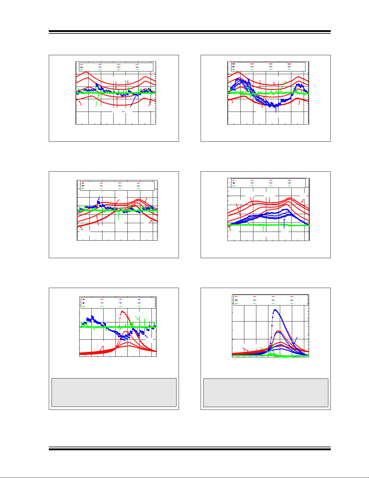
FIGURE 2-51: 50 kΩ : Write Wiper (40h →
3Fh) Settling Time (V
FIGURE 2-52: 50 k
3Fh) Settling Time (V
=5.5V).
DD
Ω
: Write Wiper (40h →
=2.7V).
DD
FIGURE 2-54: 50 k
00h) Settling Time (V
FIGURE 2-55: 50 k
00h) Settling Time (V
DD
DD
Ω
: Write Wiper (FFh →
=5.5V).
Ω
: Write Wiper (FFh →
=2.7V).
Ω
FIGURE 2-53: 50 k
3Fh) Settling Time (V
DS22147A-page 22 © 2009 Microchip Technology Inc.
: Write Wiper (40h →
=1.8V).
DD
FIGURE 2-56: 50 k
00h) Settling Time (V
Ω
: Write Wiper (FFh →
=1.8V).
DD

Note: Unless otherwise indicated, TA = +25°C, VDD = 5V, VSS = 0V.
20
40
60
80
100
120
0 326496
Wiper Setting (decimal)
Wiper Resistance (R
W
(ohms)
-0.3
-0.2
-0.1
0
0.1
0.2
0.3
Error (LSb)
-40C Rw 25C Rw 85C Rw 125C Rw
-40C INL 25C INL 85C INL 125C INL
-40C DNL 25C DNL 85C DNL 125C DNL
INL
DNL
R
W
-40°C
25°C
85°C
125°C
20
60
100
140
180
220
260
300
0326496
Wiper Setting (decimal)
Wiper Resistance (R
W
(ohms)
-0.3
-0.2
-0.1
0
0.1
0.2
0.3
Error (LSb)
-40C Rw 25C Rw 85C Rw 125C Rw
-40C INL 25C INL 85C INL 125C I NL
-40C DNL 25C DNL 85C DNL 125C DNL
INL
DNL
-40°C
25°C
85°
R
W
125°C
Note: Refer to AN1080 for additional informa-
tion on the characteristics of the wiper
resistance (R
W
) with respect to device
voltage and wiper setting value.
0
2500
5000
7500
10000
12500
15000
0326496
Wiper Setting (decimal)
Wiper Resistance (R
W
(ohms)
-0.35
-0.25
-0.15
-0.05
0.05
0.15
0.25
0.35
Error (LSb)
-40C Rw 25C Rw 85C Rw 125C Rw
-40C INL 25C INL 85C INL 125C INL
-40C DNL 25C DNL 85C DNL 125C DNL
INL
DNL
RW
20
40
60
80
100
120
0 326496
Wiper Setting (decimal)
Wiper Resistance (R
W
(ohms)
-0.3
-0.2
-0.1
0
0.1
0.2
0.3
Error (LSb)
-40C Rw 25C Rw 85C Rw 125C Rw
-40C INL 25C INL 85C INL 125C INL
-40C DNL 25C DNL 85C DNL 125C DNL
INL
DNL
R
-40°C
25°C
85°C
125°C
20
60
100
140
180
220
260
300
0 326496
Wiper Setting (decimal)
Wiper Resistance (R
W
(ohms)
-0.3
-0.2
-0.1
0
0.1
0.2
0.3
Error (LSb)
-40C Rw 25C Rw 85C Rw 125C Rw
-40C INL 25C INL 85C INL 125C INL
-40C DNL 25C DNL 85C DNL 125C DNL
INL
DNL
R
W
-40°C
25°C
85°C
125°C
Note: Refer to AN1080 for additional informa-
tion on the characteristics of the wiper
resistance (R
W
) with respect to device
voltage and wiper setting value.
0
2500
5000
7500
10000
12500
15000
0326496
Wiper Setting (decimal)
Wiper Resistance (R
W
(ohms)
-1
1
3
5
7
9
11
13
15
17
19
Error (LSb)
-40C Rw 25C Rw 85C Rw 125C Rw
-40C INL 25C INL 85C INL 125C INL
-40C DNL 25C DNL 85C DNL 125C DNL
INL
DNL
RW
MCP4017/18/19
)
FIGURE 2-57: 100 kΩ Pot Mode : RW (Ω),
INL (LSb), DNL (LSb) vs. Wiper Setting and
Temperature (V
)
= 5.5V).
DD
)
W
FIGURE 2-60: 100 k
(
Ω
), INL (LSb), DNL (LSb) vs. Wiper Setting and
Temperature (V
)
= 5.5V). (IW = 45uA, B = VSS)
DD
Ω
Rheo Mode : RW
FIGURE 2-58: 100 k
INL (LSb), DNL (LSb) vs. Wiper Setting and
Temperature (V
)
FIGURE 2-59: 100 k
INL (LSb), DNL (LSb) vs. Wiper Setting and
Temperature (V
© 2009 Microchip Technology Inc. DS22147A-page 23
DD
DD
= 2.7V).
= 1.8V).
Ω
Pot Mode : RW (Ω),
Ω
Pot Mode : RW (Ω),
Ω
FIGURE 2-61: 100 k
(
Ω
), INL (LSb), DNL (LSb) vs. Wiper Setting and
Temperature (V
)
= 2.7V). (IW = 21uA, B = VSS)
DD
FIGURE 2-62: 100 k
(
Ω
), INL (LSb), DNL (LSb) vs. Wiper Setting and
Temperature (V
= 1.8V). (IW = TBD, B = VSS)
DD
Rheo Mode : RW
Ω
Rheo Mode : RW

MCP4017/18/19
-0.08
-0.06
-0.04
-0.02
0.00
-40 0 40 80 120
Ambient Temperature (°C)
Full-Scale Error (FSE) (LSb)
2.7
5.5V
1.8V
0.00
0.04
0.08
0.12
-40 0 40 80 120
Ambient Temperature (°C)
Zero-Scale Error (ZSE) (LSb)
2.7
5.5V
1.8V
97800
98000
98200
98400
98600
98800
99000
99200
99400
99600
99800
-40 0 40 80 120
Ambient Temperature (°C)
Nominal Resistance (R
AB
(Ohms)
2.7V
5.5V
1.8V
0
20
40
60
80
100
0 326496
Wiper Setting (decimal)
R
BW
Tempco (PPM)
2.7V
5.5V
Wiper
V
DD
Note: Unless otherwise indicated, TA = +25°C, VDD = 5V, VSS = 0V.
FIGURE 2-63: 100 kΩ : Full Scale Error
(FSE) vs. Temperature (V
FIGURE 2-64: 100 k
(ZSE) vs. Temperature (V
)
= 5.5V, 2.7V, 1.8V).
DD
Ω
: Zero Scale Error
= 5.5V, 2.7V, 1.8V).
DD
FIGURE 2-66: 100 k
Δ
RWB / ΔT vs. Code.
FIGURE 2-67: 100 k
Response Time.
Ω
: RBW Tempco
Ω
: Power-Up Wiper
FIGURE 2-65: 100 k
Resistance (
DS22147A-page 24 © 2009 Microchip Technology Inc.
Ω
) vs. Temperature and VDD.
Ω
: Nominal
Ω
FIGURE 2-68: 100 k
: Digital
Feedthrough (SCL signal coupling to Wiper pin).

Note: Unless otherwise indicated, TA = +25°C, VDD = 5V, VSS = 0V.
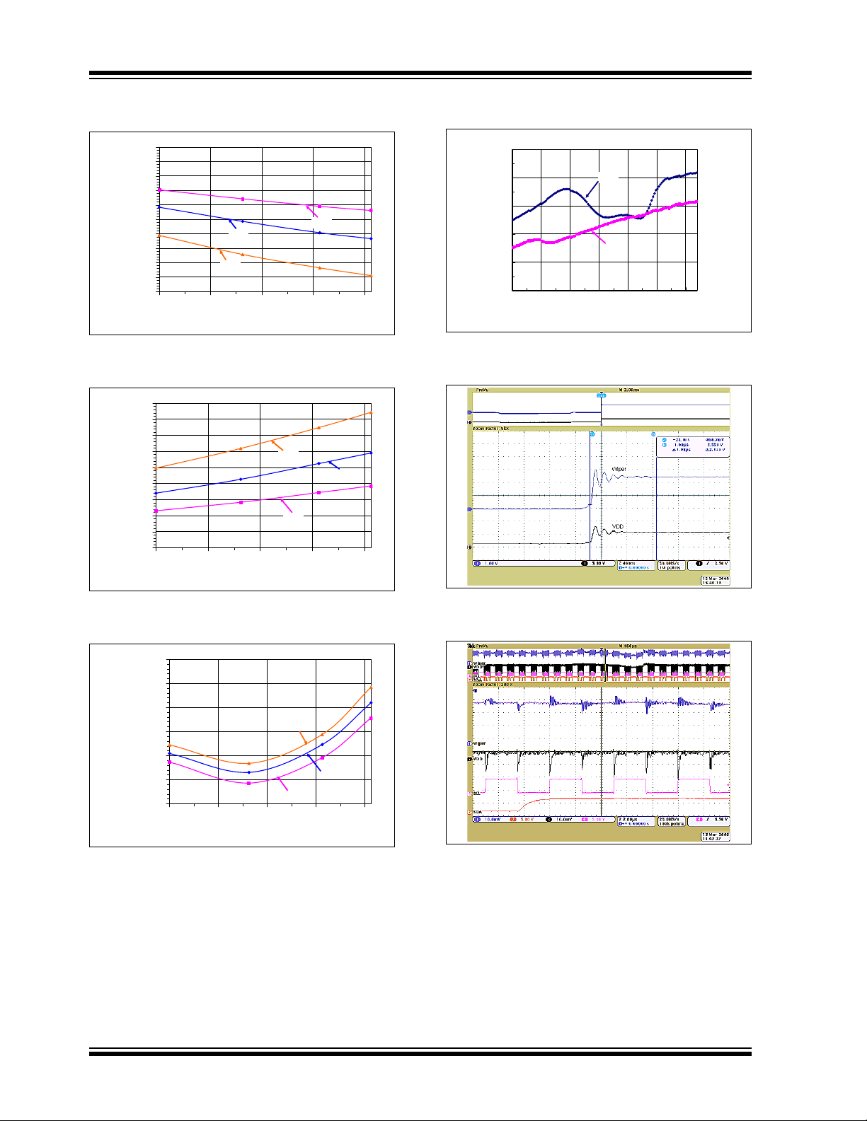
MCP4017/18/19
FIGURE 2-69: 100 kΩ : Write Wiper (40h
→
3Fh) Settling Time (V
FIGURE 2-70: 100 k
→
3Fh) Settling Time (V
= 5.5V).
DD
Ω
: Write Wiper (40h
= 2.7V).
DD
FIGURE 2-72: 100 k
→
00h) Settling Time (V
FIGURE 2-73: 100 k
→
00h) Settling Time (V
DD
DD
Ω
: Write Wiper (FFh
= 5.5V).
Ω
: Write Wiper (FFh
= 2.7V).
Ω
FIGURE 2-71: 100 k
→
3Fh) Settling Time (V
© 2009 Microchip Technology Inc. DS22147A-page 25
: Write Wiper (40h
= 1.8V).
DD
FIGURE 2-74: 100 k
→
00h) Settling Time (V
Ω
: Write Wiper (FFh
= 1.8V).
DD

MCP4017/18/19
0
0.5
1
1.5
2
2.5
3
3.5
4
-40 0 40 80 120
Temperature (°C)
V
IH
(V)
5.5V
2.7V
1.8V
0
0.5
1
1.5
2
-40 0 40 80 120
Temperature (°C)
V
IL
(V)
5.5V
2.7V
1.8V
0
0.05
0.1
0.15
0.2
0.25
0.3
-40 0 40 80 120
Temperature (°C)
V
OL
(mV)
5.5V (@ 3mA)
2.7V (@ 3mA)
1.8V (@ 1mA)
0
0.2
0.4
0.6
0.8
1
1.2
-40 0 40 80 120
Temperature (°C)
V
DD
(V)
5.5
2.7V
Note: Unless otherwise indicated, TA = +25°C, VDD = 5V, VSS = 0V.
FIGURE 2-75: VIH (SCL, SDA) vs. VDD and Temperature.
FIGURE 2-76: V
(SCL, SDA) vs. VDD and
IL
Temperature.
FIGURE 2-77: V
(SDA) vs. VDD and
OL
Temperature.
FIGURE 2-78: POR/BOR Trip point vs. V
and Temperature.
DD
DS22147A-page 26 © 2009 Microchip Technology Inc.

Note: Unless otherwise indicated, TA = +25°C, VDD = 5V, VSS = 0V.
-50
-40
-30
-20
-10
0
10
100 1,000 10,000
Frequency (kHz)
dB
Code = 7Fh
Code = 3Fh
Code = 01h
Code = 0Fh
Code = 1Fh
-60
-50
-40
-30
-20
-10
0
10
100 1,000 10,000
Frequency (kHz)
dB
Code = 7Fh
Code = 3Fh
Code = 01h
Code = 0Fh
Code = 1Fh
-60
-50
-40
-30
-20
-10
0
10
100 1,000 10,000
Frequency (kHz)
dB
Code = 7Fh
Code = 3Fh
Code = 0Fh
Code = 1Fh
Code = 01h
-60
-50
-40
-30
-20
-10
0
10
100 1,000 10,000
Frequency (kHz)
dB
Code = 7Fh
Code = 3Fh
Code = 0Fh
Code = 1Fh
Code = 01h
+
-
V
OUT
+5V
A
B
W
V
IN
+5V
MCP4017/18/19
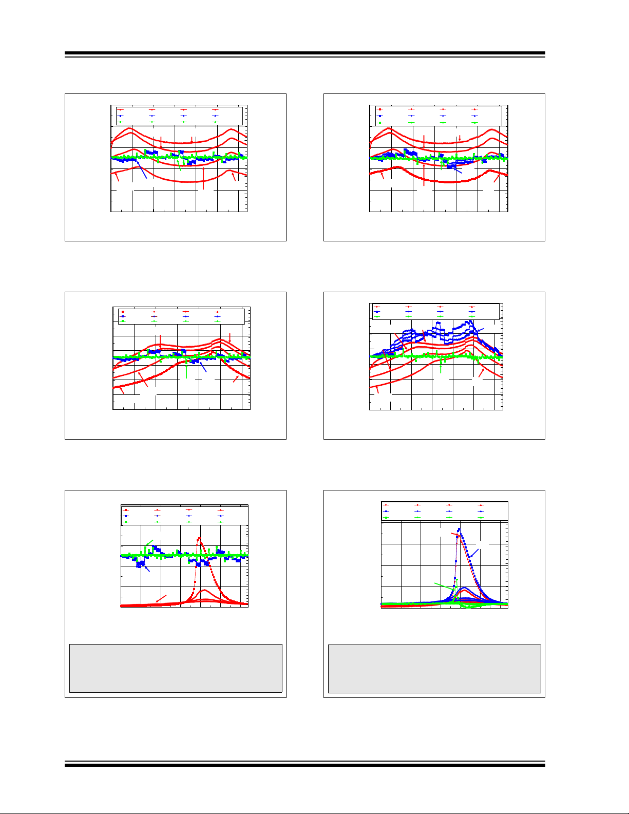
FIGURE 2-79: 5kΩ – Gain vs. Frequency
(-3dB).
Ω
FIGURE 2-80: 10 k
– Gain vs. Frequency
(-3dB).
FIGURE 2-82: 100 k
Ω
– Gain vs.
Frequency (-3dB).
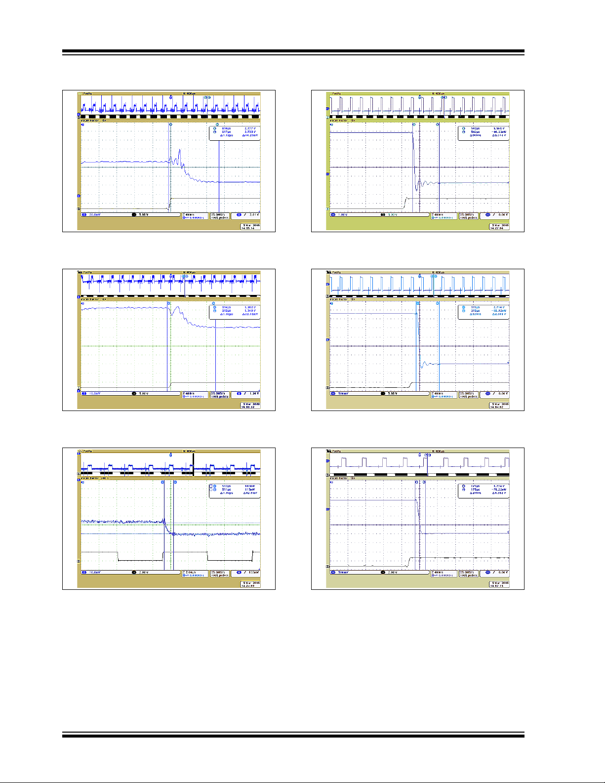
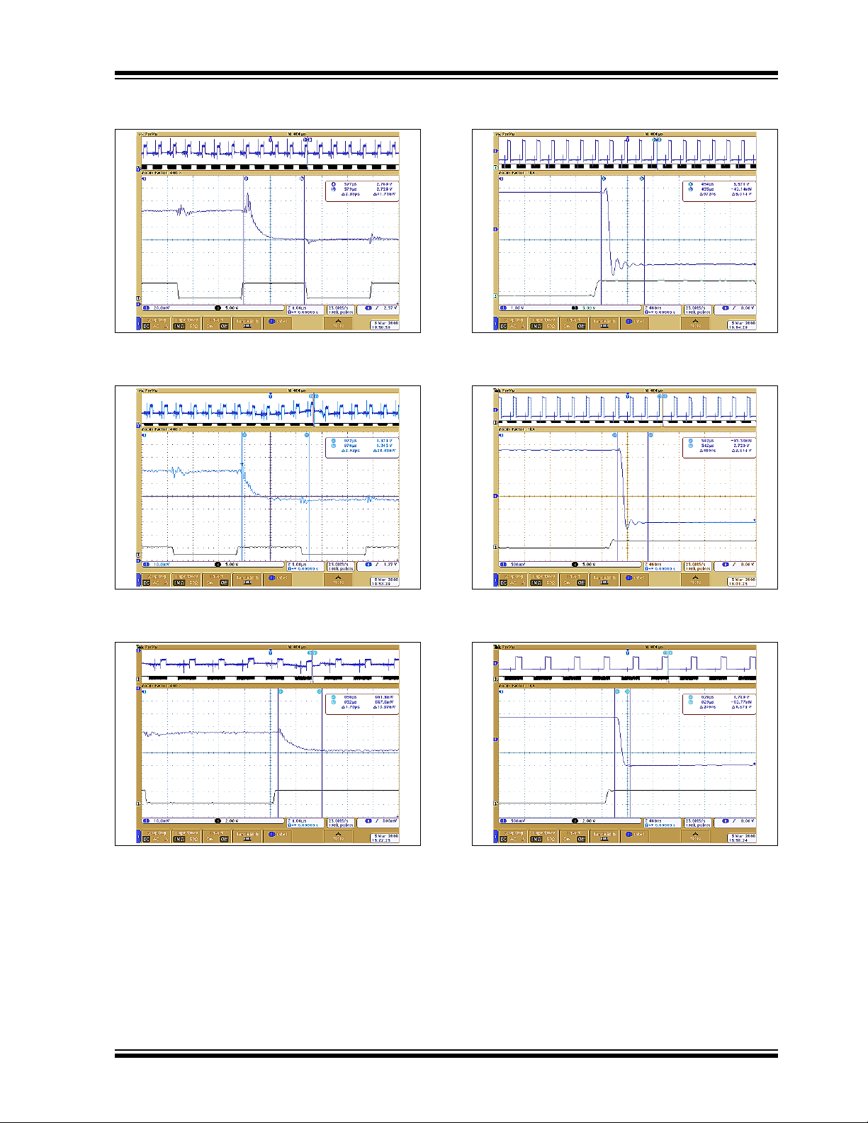
2.1 Test Circuits
FIGURE 2-83: Gain vs. Frequency Test (-3dB).
FIGURE 2-81: 50 k
(-3dB).
© 2009 Microchip Technology Inc. DS22147A-page 27
Ω
– Gain vs. Frequency

MCP4017/18/19
NOTES:
DS22147A-page 28 © 2009 Microchip Technology Inc.

3.0 PIN DESCRIPTIONS
The descriptions of the pins are listed in Ta b le 3- 1.
Additional descriptions of the device pins follow.
TABLE 3-1: PINOUT DESCRIPTION FOR THE MCP4017/18/19
MCP4017/18/19
Pin
Name
V
V
SCL333I/OST (OD)I
SDA444I/OST (OD)I
Legend: A = Analog input ST (OD) = Schmitt Trigger with Open Drain
MCP4017
(SC70-6)
DD
SS
B 5 — — I/O A Potentiometer Terminal B
W 6 5 5 I/O A Potentiometer Wiper Terminal
A — 6 — I/O A Potentiometer Terminal A
I = Input O = Output I/O = Input/Output P = Power
Pin Number
MCP4018
(SC70-6)
1 1 1 P — Positive Power Supply Input
2 2 2 P — Ground
MCP4019
(SC70-5)
Pin
Typ e
Buffer
Type
Function
2
C Serial Clock pin
2
C Serial Data pin
© 2009 Microchip Technology Inc. DS22147A-page 29

MCP4017/18/19
3.1 Positive Power Supply Input (VDD)
The VDD pin is the device’s positive power supply input.
The input power supply is relative to V
from 1.8V to 5.5V. A de-coupling capacitor on VDD (to
VSS) is recommended to achieve maximum
performance.
While the device’s voltage is in the range of 1.8V ≤ V
< 2.7V, the Resistor Network’s electrical performance
of the device may not meet the data sheet
specifications.
and can range
SS
DD
3.2 Ground (VSS)
The VSS pin is the device ground reference.
3.3 I2C Serial Clock (SCL)
The SCL pin is the serial clock pin of the I2C interface.
The MCP401X acts only as a slave and the SCL pin
accepts only external serial clocks. The SCL pin is an
open-drain output. Refer to Section 5.0 “Serial
Interface - I
Interface communication.
2
C Module” for more details of I2C Serial
3.4 I2C Serial Data (SDA)
W pin can support both positive and negative current.
The voltage on terminal W must be between V
VDD.
SS
and
3.7 Potentiometer Terminal A
The terminal A pin (available on some devices) is
connected to the internal potentiometer’s terminal A.
The potentiometer’s terminal A is the fixed connection
to the Full Scale (0x7F tap) wiper value of the digital
potentiometer.
The terminal A pin is available on the MCP4018
devices. The terminal A pin does not have a polarity
relative to the terminal W pin. The terminal A pin can
support both positive and negative current. The voltage
on Terminal A must be between V
The terminal A pin is not available on the MCP4017
and MCP4019 devices. For these devices, the
potentiometer’s terminal A is internally floating.
and VDD.
SS
The SDA pin is the serial data pin of the I2C interface.
The SDA pin has a Schmitt trigger input and an
open-drain output. Refer to Section 5.0 “Serial
Interface - I
Interface communication.
2
C Module” for more details of I2C Serial
3.5 Potentiometer Terminal B
The terminal B pin (available on some devices) is
connected to the internal potentiometer’s terminal B.
The potentiometer’s terminal B is the fixed connection
to the Zero Scale (0x00 tap) wiper value of the digital
potentiometer.
The terminal B pin is available on the MCP4017 device.
The terminal B pin does not have a polarity relative to
the terminal W pin. The terminal B pin can support both
positive and negative current. The voltage on terminal
B must be between V
The terminal B pin is not available on the MCP4018
and MCP4019 devices. For these devices, the
potentiometer’s terminal B is internally connected to
.
V
SS
and VDD.
SS
3.6 Potentiometer Wiper (W) Terminal
The terminal W pin is connected to the internal
potentiometer’s terminal W (the wiper). The wiper
terminal is the adjustable terminal of the digital
potentiometer. The terminal W pin does not have a
polarity relative to terminals A or B pins. The terminal
DS22147A-page 30 © 2009 Microchip Technology Inc.

MCP4017/18/19
4.0 GENERAL OVERVIEW
The MCP4017/18/19 devices are general purpose
digital potentiometers intended to be used in
applications where a programmable resistance with
moderate bandwidth is desired.
This Data Sheet covers a family of three Digital
Potentiometer and Rheostat devices. The MCP4018
device is the Potentiometer configuration, while the
MCP4017 and MCP4019 devices are the Rheostat
configuration.
Applications generally suited for the MCP401X devices
include:
• Set point or offset trimming
• Sensor calibration
• Selectable gain and offset amplifier designs
• Cost-sensitive mechanical trim pot replacement
As the Device Block Diagram shows, there are four
main functional blocks. These are:
• POR/BOR Operation
• Serial Interface - I
• Resistor Network
The POR/BOR operation and the Memory Map are
discussed in this section and the I
Network operation are described in their own sections.
The Serial Commands commands are discussed in
Section 5.4.
4.1 POR/BOR Operation
The Power-on Reset is the case where the device is
having power applied to it from VSS. The Brown-out
Reset occurs when a device had power applied to it,
and that power (voltage) drops below the specified
range.
The devices RAM retention voltage (V
than the POR/BOR voltage trip point (V
maximum V
When V
electrical performance may not meet the data sheet
specifications. In this region, the device is capable of
reading and writing to its volatile memory if the proper
serial command is executed.
Table 4-1 shows the digital pot’s level of functionality
across the entire V
the Power-up and Brown-out functionality.
POR/VBOR
POR/VBOR
2
C Module
2
C and Resistor
) is lower
RAM
POR/VBOR
). The
voltage is less then 1.8V.
< VDD < 2.7V, the Resistor Network’s
range, while Figure 4-1 illustrates
DD
4.1.2 BROWN-OUT RESET
When the device powers down, the device VDD will
cross the V
POR/VBOR
decreases below the V
voltage. Once the VDD voltage
POR/VBOR
voltage the following
happens:
• Serial Interface is disabled
If the VDD voltage decreases below the V
RAM
voltage
the following happens:
• Volatile wiper registers may become corrupted
As the voltage recovers above the V
POR/VBOR
voltage
see Section 4.1.1 “Power-on Reset”.
Serial commands not completed due to a Brown-out
condition may cause the memory location to become
corrupted.
4.1.3 WIPER REGISTER (RAM)
The Wiper Register is volatile memory that starts
functioning at the RAM retention voltage (V
RAM
). The
Wiper Register will be loaded with the default wiper
value when V
will rise above the V
DD
POR/VBOR
voltage.
4.1.4 DEVICE CURRENTS
The current of the device can be classified into two
modes of the device operation. These are:
• Serial Interface Inactive (Static Operation)
• Serial Interface Active
Static Operation occurs when a Stop condition is
received. Static Operation is exited when a Start
condition is received.
4.1.1 POWER-ON RESET
When the device powers up, the device VDD will cross
the V
POR/VBOR
the V
POR/VBOR
• Volatile wiper register is loaded with the default
wiper value (3Fh)
• The device is capable of digital operation
© 2009 Microchip Technology Inc. DS22147A-page 31
voltage. Once the VDD voltage crosses
voltage, the following happens:

MCP4017/18/19
V
POR/BOR
V
SS
V
DD
2.7V
Outside Specified
Normal Operation Range
Device’s Serial
Wiper Forced to Default POR/BOR setting
V
BOR
Delay
Normal Operation Range
1.8V
Interface is
“Not Operational”
AC/DC Range
Analog
Characteristics
not specified
Analog
Characteristics not specified
V
RAM
TABLE 4-1: DEVICE FUNCTIONALITY AT EACH VDD REGION (NOTE 1)
VDD Level
< V
V
DD
V
BOR
1.8V ≤ V
2.7V ≤ V
< 1.8V Ignored “unknown” Unknown
BOR
≤ VDD < 1.8V “Unknown” Operational with
< 2.7V Accepted Operational with
DD
≤ 5.5V Accepted Operational Wiper Register
DD
Serial
Interface
Note 1: For system voltages below the minimum operating voltage, the customer will be recommended to use a
voltage supervisor to hold the system in reset. This will ensure that MCP4017/18/19 commands are not
attempted out of the operating range of the device.
Potentiometer
Terminals
reduced electrical
specs
reduced electrical
specs
Wiper Setting Comment
Wiper Register loaded
with POR/BOR value
Wiper Register
determines Wiper
Electrical performance may not
meet the data sheet specifications.
Setting
Meets the data sheet specifications
determines Wiper
Setting
FIGURE 4-1: Power-up and Brown-out.
DS22147A-page 32 © 2009 Microchip Technology Inc.

MCP4017/18/19
Single I2C Bus Configuration
Host
Controller
Device 1
Device 3
Device n
Device 2
Device 4
5.0 SERIAL INTERFACE I2C MODULE
A 2-wire I2C serial protocol is used to write or read the
digital potentiometer’s wiper register. The I
utilizes the SCL input pin and SDA input/output pin.
2
C serial interface supports the following features.
The I
• Slave mode of operation
• 7-bit addressing
• The following clock rate modes are supported:
- Standard mode, bit rates up to 100 kb/s
- Fast mode, bit rates up to 400 kb/s
• Support Multi-Master Applications
The serial clock is generated by the Master.
2
C Module is compatible with the Phillips I2C
The I
specification. Phillips only defines the field types, field
lengths, timings, etc. of a frame. The frame content
defines the behavior of the device. The frame content
for the MCP4017, MCP4018, and MCP4019 devices
are defined in this section of the Data Sheet.
2
Figure 5-1 shows a typical I
C bus configurations.
2
C protocol
5.1 I2C I/O Considerations
I2C specifications require active low, passive high
functionality on devices interfacing to the bus. Since
devices may be operating on separate power supply
sources, ESD clamping diodes are not permitted. The
specification recommends using open drain transistors
tied to V
specification makes some general recommendations
on the size of this pull-up, but does not specify the
exact value since bus speeds and bus capacitance
impacts the pull-up value for optimum system
performance.
Common pull-up values range from 1 k
~10 kΩ. Power sensitive applications tend to choose
higher values to minimize current losses during
communication but these applications also typically
utilize lower V
The SDA and SCL float (are not driving) when the
device is powered down.
A "glitch" filter is on the SCL and SDA pins when the pin
is an input. When these pins are an output, there is a
slew rate control of the pin that is independent of device
frequency.
5.1.1 SLOPE CONTROL
The device implements slope control on the SDA
output. The slope control is defined by the fast mode
specifications.
For Fast (FS) mode, the device has spike suppression
and Schmidt trigger inputs on the SDA and SCL pins.
(common) with a pull-up resistor. The
SS
Ω to a max of
.
DD
FIGURE 5-1: Typical Application I2C Bus Configurations.
Refer to Section 2.0 “Typical Performance Curves”,
AC/DC Electrical Characteristics table for detailed input
threshold and timing specifications.
© 2009 Microchip Technology Inc. DS22147A-page 33

MCP4017/18/19
SDA
SCL
S
1st Bit
2nd Bit
SDA
SCL
S
1st Bit
2nd Bit
A
8
D0
9
SDA
SCL
SDA
SCL
Sr = Repeated Start
1st Bit
5.2 I2C Bit Definitions
I2C bit definitions include:
• Start Bit
• Data Bit
• Acknowledge (A) Bit
• Repeated Start Bit
• Stop Bit
• Clock Stretching
Figure 5-8 shows the waveform for these states.
5.2.1 START BIT
The Start bit (see Figure 5-2) indicates the beginning of
a data transfer sequence. The Start bit is defined as the
SDA signal falling when the SCL signal is “High”.
FIGURE 5-2: Start Bit.
5.2.2 DATA BIT
The SDA signal may change state while the SCL signal
is Low. While the SCL signal is High, the SDA signal
MUST be stable (see Figure 5-3).
FIGURE 5-3: Data Bit.
5.2.3 ACKNOWLEDGE (A) BIT
The A bit (see Figure 5-4) is a response from the Slave
device to the Master device. Depending on the context
of the transfer sequence, the A bit may indicate
different things. Typically the Slave device will supply
an A response after the Start bit and 8 “data” bits have
been received. The A bit will have the SDA signal low.
If the Slave Address is not valid, the Slave Device will
issue a Not A (A). The A bit will have the SDA signal
high.
If an error condition occurs (such as an A
then an START bit must be issued to reset the
command state machine.
instead of A)
TABLE 5-1: MCP4017/18/19 A / A
RESPONSES
Event
General Call A
Slave Address
valid
Slave Address
not valid
Bus Collision N.A. I
Acknowledge
Bit Response
A
A
Comment
2
C Module Resets,
or a “Don’t Care” if
the collision occurs
on the Masters
“Start bit”.
5.2.4 REPEATED START BIT
The Repeated Start bit (see Figure 5-5) indicates the
current Master Device wishes to continue
communicating with the current Slave Device without
releasing the I
the same as the Start condition, except that the
Repeated Start bit follows a Start bit (with the Data bits
+ A bit) and not a Stop bit.
The Start bit is the beginning of a data transfer
sequence and is defined as the SDA signal falling when
the SCL signal is “High”.
Note 1: A bus collision during the Repeated Start
2
C bus. The Repeated Start condition is
condition occurs if:
• SDA is sampled low when SCL goes
from low to high.
• SCL goes low before SDA is asserted
low. This may indicate that another master is attempting to transmit a data "1".
FIGURE 5-4: Acknowledge Waveform.
FIGURE 5-5: Repeat Start Condition
Waveform.
DS22147A-page 34 © 2009 Microchip Technology Inc.

MCP4017/18/19
SCL
SDA
A / A
P
1st
SDA
SCL
S 2nd 3rd 4th 5th 6th 7th 8th PA/A
Bit Bit Bit Bit Bit Bit Bit Bit
1st 2nd 3rd 4th 5th 6th 7th 8th A/A
Bit Bit Bit Bit Bit Bit Bit Bit
SCL
SDA
START
Condition
STOP
Condition
Data allowed
to change
Data or
A valid
5.2.5 STOP BIT
The Stop bit (see Figure 5-6) Indicates the end of the
2
C Data Transfer Sequence. The Stop bit is defined as
I
the SDA signal rising when the SCL signal is “High”.
2
A Stop bit resets the I
C interface of the other devices.
FIGURE 5-6: Stop Condition Receive or Transmit Mode.
5.2.6 CLOCK STRETCHING
“Clock Stretching” is something that the Secondary
Device can do, to allow additional time to “respond” to
the “data” that has been received.
The MCP4017/18/19 will not strech the clock signal
(SCL) since memory read accesses occur fast enough.
5.2.7 ABORTING A TRANSMISSION
If any part of the I2C transmission does not meet the
command format, it is aborted. This can be intentionally
accomplished with a START or STOP condition. This is
done so that noisy transmissions (usually an extra
START or STOP condition) are aborted before they
corrupt the device.
5.2.8 IGNORING AN I2C TRANSMISSION
AND “FALLING OFF” THE BUS
The MCP4017/18/19 expects to receive entire, valid
I2C commands and will assume any command not
defined as a valid command is due to a bus corruption
and will enter a passive high condition on the SDA
signal. All signals will be ignored until the next valid
START condition and CONTROL BYTE are received.
FIGURE 5-7: Typical 16-bit I2C Waveform Format.
2
FIGURE 5-8: I
C Data States and Bit Sequence.
© 2009 Microchip Technology Inc. DS22147A-page 35

MCP4017/18/19
SA6A5A4A3A2A1A0R/W
A/A
Start
bit
Slave Address
R/W bit
A bit (controlled by slave device)
R/W = 0 = write
R/W = 1 = read
A = 0 = Slave Device Acknowledges byte
A
= 1 = Slave Device does not Acknowledge byte
“0” “1” “0” “1” “1” “1” “1”
0000S 0000 XxxxxAxx0AP
General Call Address
Second Byte
“7-bit Command”
Reserved 7-bit Commands (By I
2
C Specification - Philips # 9398 393 40011, Ver. 2.1 January 2000)
‘0000 011’b - Reset and write programmable part of slave address by hardware.
‘0000 010’b - Write programmable part of slave address by hardware.
‘0000 000’b - NOT Allowed
The Following is a “Hardware General Call” Format
0000S 0000 XxxxxA xx1A
General Call Address
Second Byte
“7-bit Command”
Xxxxx xxXAP
n occurrences of (Data + A / A)
This indicates a “Hardware General Call”
MCP4016/7/8/9 will ignore this byte and
all following bytes (and A), until
a Stop bit (P) is encountered.
5.2.9 I2C COMMAND PROTOCOL
The MCP4017/18/19 is a slave I2C device which
supports 7-bit slave addressing. The slave address
contains seven fixed bits. Figure 5-9 shows the control
byte format.
5.2.9.1 Control Byte (Slave Address)
The Control Byte is always preceded by a START
condition. The Control Byte contains the slave address
consisting of seven fixed bits and the R/W bit. Figure 5-
9 shows the control byte format and Table 5-2 shows
2
C address for the devices.
the I
TABLE 5-2: DEVICE I
Device I2C Address Comment
MCP4017 ‘0101111’
MCP4018 ‘0101111’
MCP4019 ‘0101111’
2
C ADDRESS
5.2.9.2 Hardware Address Pins
The MCP4017/MCP4018/MCP4019 does not support
hardware address bits.
5.2.10 GENERAL CALL
The General Call is a method that the Master device
can communicate with all other Slave devices.
The MCP4017/18/19 devices do not respond to
General Call address and commands, and therefore
the communications are Not Acknowledged.
FIGURE 5-9: Slave Address Bits in the
2
I
C Control Byte.
FIGURE 5-10: General Call Formats.
DS22147A-page 36 © 2009 Microchip Technology Inc.

5.3 Software Reset Sequence
S ‘1’ ‘1’ ‘1’ ‘1’ ‘1’ ‘1’ ‘1’ ‘1’ S P
Start
bit
Nine bits of ‘1’
Start bit
Stop bit
Note: This technique should be supported by
any I2C compliant device. The 24xxxx I2C
Serial EEPROM devices support this technique, which is documented in AN1028.
MCP4017/18/19
2
The Stop bit terminates the current I
MCP4017/18/19 wait to detect the next Start condition.
This sequence does not effect any other I
which may be on the bus, as they should disregard this
as an invalid command.
C bus activity. The
2
C devices
At times it may become necessary to perform a
Software Reset Sequence to ensure the MCP4017/18/
19 device is in a correct and known I
This only resets the I2C state machine.
This is useful if the MCP4017/18/19 device powers up
in an incorrect state (due to excessive bus noise, etc),
or if the Master Device is reset during communication.
Figure 5-11 shows the communication sequence to
software reset the device.
2
C Interface state.
FIGURE 5-11: Software Reset Sequence Format.
The 1st Start bit will cause the device to reset from a
state in which it is expecting to receive data from the
Master Device.In this mode, the device is monitoring
the data bus in Receive mode and can detect the Start
bit forces an internal Reset.
The nine bits of ‘1’ are used to force a Reset of those
devices that could not be reset by the previous Start bit.
This occurs only if the MCP4017/18/19 is driving an A
on the I
command) and is driving a data bit of ‘0’ onto the I2C
bus. In both of these cases, the previous Start bit could
not be generated due to the MCP4017/18/19 holding
the bus low. By sending out nine ‘1’ bits, it is ensured
that the device will see a A
drive the I
the MCP4017/18/19), which also forces the MCP4017/
18/19 to reset.
The 2nd Start bit is sent to address the rare possibility
of an erroneous write. This could occur if the Master
Device was reset while sending a Write command to
the MCP4017/18/19, AND then as the Master Device
returns to normal operation and issues a Start condition
while the MCP4017/18/19 is issuing an A. In this case
if the 2nd Start bit is not sent (and the Stop bit was sent)
the MCP4017/18/19 could initiate a write cycle.
2
C bus, or is in output mode (from a Read
2
C bus low to acknowledge the data sent by
Note: The potential for this erroneous write
ONLY occurs if the Master Device is reset
while sending a Write command to the
MCP4017/18/19.
(the Master Device does not
5.4 Serial Commands
The MCP4017/18/19 devices support 2 serial
commands. These commands are:
• Write Operation
• Read Operations
© 2009 Microchip Technology Inc. DS22147A-page 37

MCP4017/18/19
STOP bit
Slave Address Byte
Data Byte Data Byte
1010S1110 D3AD2D1D0AD3xD6D5D4 D2D1D0A
Fixed
Address
Data Byte Data Byte
AD3x D6D5D4 D2D1D0 A
P
Read/Write bit (“0” = Write)
xD6D5D4
D3 D2 D1 D0
xD6D5D4
S = Start Condition
P = Stop Condition
A = Acknowledge
X = Don’t Care
R/W = Read/Write bit
D6, D5, D4, D3, D2, D1, D0 = Data bits
Legend
5.4.1 WRITE OPERATION
The write operation requires the START condition,
Control Byte, Acknowledge, Data Byte, Acknowledge
and STOP (or RESTART) condition. The Control (Slave
Address) Byte requires the R/W
= “0”) to generate a write sequence. The
(R/W
MCP4017/18/19 is responsible for generating the
Acknowledge (A) bits.
Data is written to the MCP4017/18/19 after every byte
transfer (during the A bit). If a STOP or RESTART
condition is generated during a data transfer (before
the A bit), the data will not be written to MCP4017/18/
19.
Data bytes may be written after each Acknowledge.
The command is terminated once a Stop (P) condition
occurs. Refer to Figure 5-12 for the write sequence.
For a single byte write, the master sends a STOP or
RESTART condition after the 1st data byte is sent.
The MSb of each Data Byte is a don’t care, since the
wiper register is only 7-bits wide.
Figure 5-14 shows the I
the Master Device and the MCP4017/18/19 device and
the resultant I2C bus values.
bit equal to a logic zero
2
C communication behavior of
5.4.2 READ OPERATIONS
The read operation requires the START condition,
Control Byte, Acknowledge, Data Byte, the master
generating the A
Byte requires the R/W bit equal to a logic one (R/W =
1) to generate a read sequence. The MCP4017/18/19
will A the Slave Address Byte and A
2
C Master will A the Slave Address Byte and the
The I
last Data Byte. If there are multiple Data Bytes, the I2C
Master will A all Data Bytes except the last Data Byte
(which it will A
The MCP4017/18/19 maintains control of the SDA
signal until all data bits have been clocked out.
The command is terminated once a Stop (P) condition
occurs. Refer to Figure 5-13 for the read command
sequence. For a single read, the master sends a STOP
or RESTART condition after the 1st data byte (and A
bit) is sent from the slave.
Figure 5-14 shows the I
the Master Device and the MCP4017/18/19 device and
the resultant I
and STOP condition. The Control
all the Data Bytes.
).
2
C communication behavior of
2
C bus values.
FIGURE 5-12: I2C Write Command Format.
DS22147A-page 38 © 2009 Microchip Technology Inc.

MCP4017/18/19
STOP bit
Slave Address Byte
Data Byte Data Byte
1010S1111 D3AD2D1D0A(1)D30D6D5D4 D2D1D0A(1)
Fixed
Address
Data Byte Data Byte
A(1) D30 D6D5D4 D2D1D0A
(2)
P
Read/Write bit (“1” = Read)
0D6D5D4
D3 D2 D1 D0
0D6D5D4
S = Start Condition
P = Stop Condition
A = Acknowledge
X = Don’t Care
R/W = Read/Write bit
Note 1 = Data bits
Legend
Note 1: Master Device is responsible for A / A signal. If a A signal occurs, the MCP4017/18/19
will abort this transfer and release the bus.
2: The Master Device will A, and the MCP4017/18/19 will release the bus so the Master Device can
generate a Stop or Repeated Start condition.
FIGURE 5-13: I2C Read Command Format.
© 2009 Microchip Technology Inc. DS22147A-page 39

MCP4017/18/19
Write 1 Byte
Write 2 Bytes
Read 1 Byte
Read 2 Bytes
S Slave Address
R
/
W A Data Byte
(1)
AP
Master S010111101xddddddd1P
MCP4017/18/19 0 0
I
2
C Bus S010111100xddddddd0P
S Slave Address
R
/
W A Data Byte
(1)
AData Byte
(1)
AP
Master S010111101xddddddd1xddddddd1P
MCP4017/18/19 0 0 0
I
2
C Bus S010111100xddddddd0xddddddd1P
S Slave Address
R
/
WA Data Byte A P
Master S010111111 1P
MCP4017/18/19 0 0 d d d d d d d 1
I
2
C Bus S0101111100ddddddd1P
S Slave Address
R
/
W A Data Byte A Data Byte A P
Master S 010111111 0 1P
MCP4017/18/19 00ddddddd1 0ddddddd1
I
2
C Bus S 0101111100ddddddd00ddddddd1 P
Note 1: For Write Commands, the MSb of the Data Byte is a don’t care since the wiper register is only 7-bits wide.
FIGURE 5-14: I2C Communication Behavior.
DS22147A-page 40 © 2009 Microchip Technology Inc.

6.0 RESISTOR NETWORK
RS
A
RS
R
S
RS
B
N = 127
N = 126
N = 125
N = 1
N = 0
RW
(1)
W
01h
Analog
Mux
RW
(1)
00h
RW
(1)
7Dh
RW
(1)
7Eh
RW
(1)
7Fh
Note 1: The wiper resistance is tap dependent.
That is, each tap selection resistance
has a small variation. This variation has
more effect on devices with smaller R
AB
resistance (5.0 kΩ).
The Resistor Network is made up of two parts. These
are:
• Resistor Ladder
•Wiper
Figure 6-1 shows a block diagram for the resistive
network.
Digital potentiometer applications can be divided into
two resistor network categories:
• Rheostat configuration
• Potentiometer (or voltage divider) configuration
The MCP4017 is a true rheostat, with terminal B and
the wiper (W) of the variable resistor available on pins.
The MCP4018 device offers a voltage divider
(potentiometer) with terminal B internally connected to
ground.
The MCP4019 device is a Rheostat device with
terminal A of the resistor floating, terminal B internally
connected to ground, and the wiper (W) available on
pin.
MCP4017/18/19
6.1 Resistor Ladder Module
The resistor ladder is a series of equal value resistors
) with a connection point (tap) between the two
(R
S
resistors. The total number of resistors in the series
(ladder) determines the RAB resistance (see Figure 6-
1). The end points of the resistor ladder are connected
to the device Terminal A and Terminal B pins. The R
(and RS) resistance has small variations over voltage
and temperature.
The Resistor Network has 127 resistors in a string
between terminal A and terminal B. This gives 7-bits of
resolution.
The wiper can be set to tap onto any of these 127
resistors thus providing 128 possible settings
(including terminal A and terminal B). This allows zero
scale to full scale connections.
A wiper setting of 00h connects the Terminal W (wiper)
to Terminal B (Zero Scale). A wiper setting of 3Fh is the
Mid scale setting. A wiper setting of 7Fh connects the
Terminal W (wiper) to Terminal A (Full Scale). Ta b le 6-
1 illustrates the full wiper setting map.
Terminal A and B as well as the wiper W do not have a
polarity. These terminals can support both positive and
negative current.
AB
FIGURE 6-1: Resistor Network Block Diagram.
TABLE 6-1: WIPER SETTING MAP
Wiper Setting Properties
07Fh Full Scale (W = A)
07Eh - 040h W = N
03Fh W = N (Mid Scale)
03Eh - 001h W = N
000h Zero Scale (W = B)
© 2009 Microchip Technology Inc. DS22147A-page 41

MCP4017/18/19
R
S
R
AB
127
---------=
R
WB
RABN
127
-------------- R
W
+=
N = 0 to 127 (decimal)
Step resistance (RS) is the resistance from one tap
setting to the next. This value will be dependent on the
RAB value that has been selected. Equation 6-1 shows
the calculation for the step resistance while Table 6-2
shows the typical step resistances for each device.
EQUATION 6-1: RS CALCULATION
Equation 6-2 illustrates the calculation used to
determine the resistance between the wiper and
terminal B.
EQUATION 6-2: RWB CALCULATION
The digital potentiometer is available in four nominal
resistances (RAB) where the nominal resistance is
defined as the resistance between terminal A and
terminal B. The four nominal resistances are 5 kΩ,
10 kΩ, 50 kΩ, and 100 kΩ.
The total resistance of the device has minimal variation
due to operating voltage (see Figure 2-11, Figure 2-29,
Figure 2-47, or Figure 2-65).
A POR/BOR event will load the Volatile Wiper register
value with the default value. Table 6-3 shows the
default values offered.
TABLE 6-3: DEFAULT FACTORY
SETTINGS SELECTION
Resistance
Code
-502 5.0 kΩ Mid-scale 3Fh
-103 10.0 kΩ Mid-scale 3Fh
-503 50.0 kΩ Mid-scale 3Fh
-104 100.0 kΩ Mid-scale 3Fh
Note 1: Custom POR/BOR Wiper Setting options
Typical
RAB Value
are available, contact the local Microchip
Sales Office for additional information.
Custom options have minimum volume
requirements.
Default POR Wiper
Setting Code
(1)
TABLE 6-2: STEP RESISTANCES
Resistance (Ω)
Part Number
MCP4017/18/19-502E
MCP4017/18/19-103E
MCP4017/18/19-503E
MCP4017/18/19-104E
Case
Min. 4000 31.496
Typical 5000 39.370
Max. 6000 47.244
Min. 8000 62.992
Typical 10000 78.740
Max. 12000 94.488
Min. 40000 314.961
Typical 50000 393.701
Max. 60000 472.441
Min. 80000 629.921
Typical 100000 787.402
Max. 120000 944.882
Tota l
(R
AB
)
Step (R
)
S
DS22147A-page 42 © 2009 Microchip Technology Inc.

MCP4017/18/19
A
B
W
Resistor
R
AW
R
BW
or
A
B
W
V
1
V
3
V
2
6.2 Resistor Configurations
6.2.1 RHEOSTAT CONFIGURATION
When used as a rheostat, two of the three digital
potentiometer’s terminals are used as a resistive
element in the circuit. With terminal W (wiper) and
either terminal A or terminal B, a variable resistor is
created. The resistance will depend on the tap setting
of the wiper (and the wiper’s resistance). The
resistance is controlled by changing the wiper setting
The unused terminal (B or A) should be left floating.
Figure 6-2 shows the two possible resistors that can be
used. Reversing the polarity of the A and B terminals
will not affect operation.
FIGURE 6-2: Rheostat Configuration.
This allows the control of the total resistance between
the two nodes. The total resistance depends on the
“starting” terminal to the Wiper terminal. So at the code
00h, the R
resistance in maximized (RAB + RW). Conversely, at the
code 3Fh, the R
R
resistance in maximized (RAB + RW).
BW
The resistance Step size (R
the resistor.
Note: To avoid damage to the internal wiper
The pinout for the rheostat devices is such that as the
wiper register is incremented, the resistance of the
resistor will increase (as measured from Terminal B to
the W Terminal).
resistance is minimal (RW), but the R
BW
resistance is minimal (RW), but the
AW
) equates to one LSb of
S
circuitry in this configuration, care should
be taken to insure the current flow never
exceeds 2.5 mA.
AW
6.2.2 POTENTIOMETER
CONFIGURATION
When used as a potentiometer, all three terminals of
the device are tied to different nodes in the circuit. This
allows the potentiometer to output a voltage
proportional to the input voltage. This configuration is
sometimes called voltage divider mode. The
potentiometer is used to provide a variable voltage by
adjusting the wiper position between the two endpoints
as shown in Figure 6-3. Reversing the polarity of the A
and B terminals will not affect operation.
FIGURE 6-3: Potentiometer Configuration.
The temperature coefficient of the RAB resistors is
minimal by design. In this configuration, the resistors all
change uniformly, so minimal variation should be seen.
The Wiper resistor temperature coefficient is different
to the R
V3 (Figure 6-3) is not dependent on this Wiper
resistance, just the ratio of the RAB resistors, so this
temperature coefficient in most cases can be ignored.
Note: To avoid damage to the internal wiper
temperature coefficient. The voltage at node
AB
circuitry in this configuration, care should
be taken to insure the current flow never
exceeds 2.5 mA.
© 2009 Microchip Technology Inc. DS22147A-page 43

MCP4017/18/19
RW
V
DD
Note: The slope of the resistance has a linear
area (at the higher voltages) and a
non-linear area (at the lower voltages).
6.3 Wiper Resistance
Wiper resistance is the series resistance of the analog
switch that connects the selected resistor ladder node
to the Wiper Terminal common signal (see Figure 6-1).
A value in the volatile wiper register selects which
analog switch to close, connecting the W terminal to
the selected node of the resistor ladder.
The resistance is dependent on the voltages on the
analog switch source, gate, and drain nodes, as well as
the device’s wiper code, temperature, and the current
through the switch. As the device voltage decreases,
the wiper resistance increases (see Figure 6-4 and
Table 6-4).
The wiper can connect directly to Terminal B or to
Terminal A. A zero scale connections, connects the
Terminal W (wiper) to Terminal B (wiper setting of
000h). A full scale connections, connects the Terminal
W (wiper) to Terminal A (wiper setting of 7Fh). In these
configurations the only resistance between the
Terminal W and the other Terminal (A or B) is that of the
analog switches.
The wiper resistance is typically measured when the
wiper is positioned at either zero scale (00h) or full
scale (3Fh).
The wiper resistance in potentiometer-generated
voltage divider applications is not a significant source
of error.
The wiper resistance in rheostat applications can
create significant nonlinearity as the wiper is moved
toward zero scale (00h). The lower the nominal
resistance, the greater the possible error.
In a rheostat configuration, this change in voltage
needs to be taken into account. Particularly for the
lower resistance devices. For the 5.0 kΩ device the
maximum wiper resistance at 5.5V is approximately
3.2% of the total resistance, while at 2.7V it is
approximately 6.5% of the total resistance.
In a potentiometer configuration, the wiper resistance
variation does not effect the output voltage seen on the
W pin.
The slope of the resistance has a linear area (at the
higher voltages) and a non-linear area (at the lower
voltages). In where resistance increases faster then the
voltage drop (at low voltages).
FIGURE 6-4: Relationship of Wiper
Resistance (R
Since there is minimal variation of the total device
resistance over voltage, at a constant temperature (see
Figure 2-11, Figure 2-29, Figure 2-47, or Figure 2-65),
the change in wiper resistance over voltage can have a
significant impact on the INL and DNL error.
) to Voltage.
W
TABLE 6-4: TYPICAL STEP RESISTANCES AND RELATIONSHIP TO WIPER RESISTANCE
Resistance (Ω)R
Typical Wiper (RW)
Total
(R
AB
5000 39.37 100 170 325 254.00% 431.80% 825.5% 2.00% 3.40% 6.50%
10000 78.74 100 170 325 127.00% 215.90% 412.75% 1.00% 1.70% 3.25%
50000 393.70 100 170 325 25.40% 43.18% 82.55% 0.20% 0.34% 0.65%
100000 787.40 100 170 325 12.70% 21.59% 41.28% 0.10% 0.17% 0.325%
Note 1: R
DS22147A-page 44 © 2009 Microchip Technology Inc.
)
2: R
Step
(RS)
S
AB
Typ ical
is the typical value. The variation of this resistance is minimal over voltage.
is the typical value. The variation of this resistance is minimal over voltage.
Max @
5.5V
Max @
2.7V
RW =
Typ ica l
/ RS (%)
W
RW = Max
@ 5.5V
(1)
R
RW = Max
@ 2.7V
RW =
Typ ical
/ RAB (%)
W
RW = Max
@ 5.5V
(2)
RW = Max
@ 2.7V

MCP4017/18/19
111
110
101
100
011
010
001
000
Digital
Input
Code
Actual
transfer
function
INL < 0
Ideal transfer
function
INL < 0
Digital Pot Output
111
110
101
100
011
010
001
000
Digital
Input
Code
Actual
transfer
function
Ideal transfer
function
Narrow code < 1 LSb
Wide code, > 1 LSb
Digital Pot Output
6.4 Operational Characteristics
Understanding the operational characteristics of the
device’s resistor components is important to the system
design.
6.4.1 ACCURACY
6.4.1.1 Integral Non-linearity (INL)
INL error for these devices is the maximum deviation
between an actual code transition point and its
corresponding ideal transition point after offset and
gain errors have been removed. These endpoints are
from 0x00 to 0x7F. Refer to Figure 6-5.
Positive INL means higher resistance than ideal.
Negative INL means lower resistance than ideal.
6.4.1.2 Differential Non-linearity (DNL)
DNL error is the measure of variations in code widths
from the ideal code width. A DNL error of zero would
imply that every code is exactly 1 LSb wide.
FIGURE 6-6: DNL Accuracy.
6.4.1.3 Ratiometric temperature coefficient
The ratiometric temperature coefficient quantifies the
error in the ratio R
This is typically the critical error when using a
potentiometer device (MCP4018) in a voltage divider
configuration.
AW/RWB
due to temperature drift.
6.4.1.4 Absolute temperature coefficient
The absolute temperature coefficient quantifies the
error in the end-to-end resistance (Nominal resistance
RAB) due to temperature drift. This is typically the
FIGURE 6-5: INL Accuracy.
© 2009 Microchip Technology Inc. DS22147A-page 45
critical error when using a rheostat device (MCP4017
and MCP4019) in an adjustable resistor configuration.

MCP4017/18/19
0x3F
0x3E
0x3D
0x03
0x02
0x01
0x00
Digital Input Code
Resistance (RBW)
R
W
(@ tap)
R
S0
R
S1
R
S3
R
S62
R
S63
RBW = RSn + R
W(@ Tap n)
n = 0
n = ?
6.4.2 MONOTONIC OPERATION
Monotonic operation means that the device’s
resistance increases with every step change (from
terminal A to terminal B or terminal B to terminal A).
The wiper resistances difference at each tap location.
When changing from one tap position to the next (either
increasing or decreasing), the ΔR
ΔRS. When this change occurs, the device voltage and
temperature are “the same” for the two tap positions.
is less then the
W
FIGURE 6-7: RBW.
DS22147A-page 46 © 2009 Microchip Technology Inc.

MCP4017/18/19
V
DD
V
DD
V
SS
V
SS
MCP4017/18/19
0.1 µF
PICmicro
®
Microcontroller
0.1 µF
SCL
SDA
W
B
A
7.0 DESIGN CONSIDERATIONS
In the design of a system with the MCP4017/18/19
devices, the following considerations should be taken
into account. These are:
• The Power Supply
• The Layout
In the design of a system with the MCP4017/18/19
devices, the following considerations should be taken
into account:
• Power Supply Considerations
• Layout Considerations
7.1 Power Supply Considerations
The typical application will require a bypass capacitor
in order to filter high-frequency noise, which can be
induced onto the power supply's traces. The bypass
capacitor helps to minimize the effect of these noise
sources on signal integrity. Figure 7-1 illustrates an
appropriate bypass strategy.
In this example, the recommended bypass capacitor
value is 0.1 µF. This capacitor should be placed as
close to the device power pin (V
4mm).
The power source supplying these devices should be
as clean as possible. If the application circuit has
separate digital and analog power supplies, V
should reside on the analog plane.
V
SS
) as possible (within
DD
DD
and
7.2 Layout Considerations
Inductively-coupled AC transients and digital switching
noise can degrade the input and output signal integrity,
potentially masking the MCP4017/18/19’s
performance. Careful board layout will minimize these
effects and increase the Signal-to-Noise Ratio (SNR).
Bench testing has shown that a multi-layer board
utilizing a low-inductance ground plane, isolated inputs,
isolated outputs and proper decoupling are critical to
achieving the performance that the silicon is capable of
providing. Particularly harsh environments may require
shielding of critical signals.
If low noise is desired, breadboards and wire-wrapped
boards are not recommended.
7.2.1 RESISTOR TEMPCO
Characterization curves of the resistor temperature
coefficient (Tempco) are shown in Figure 2-11,
Figure 2-29, Figure 2-47, and Figure 2-65.
These curves show that the resistor network is
designed to correct for the change in resistance as
temperature increases. This technique reduces the
end to end change is R
resistance.
AB
FIGURE 7-1: Typical Microcontroller Connections.
© 2009 Microchip Technology Inc. DS22147A-page 47

MCP4017/18/19
NOTES:
DS22147A-page 48 © 2009 Microchip Technology Inc.

8.0 APPLICATIONS EXAMPLES
V
TRIPVDD
R
WB
R1R2+
------------------
⎝⎠
⎛⎞
=
D = Digital Potentiometer Wiper Setting (0-127)
R
AB
= R
Nominal
R
WB
= RAB •
D
127
D = • (R1 + RAB ) • 127
V
TRIP
V
DD
V
DD
V
OUT
A
R
1
W
B
MCP4018
SDA
SCL
V
TRIP
0.1 µF
Comparator
V
CC+
V
CC–
V
DD
R
sense
R
1
B
A
V
DD
W
MCP4018
SDA
SCL
MCP6021
Digital potentiometers have a multitude of practical
uses in modern electronic circuits. The most popular
uses include precision calibration of set point
thresholds, sensor trimming, LCD bias trimming, audio
attenuation, adjustable power supplies, motor control
overcurrent trip setting, adjustable gain amplifiers and
offset trimming. The MCP4017/18/19 devices can be
used to replace the common mechanical trim pot in
applications where the operating and terminal voltages
are within CMOS process limitations (V
5.5V).
8.1 Set Point Threshold Trimming
= 2.7V to
DD
MCP4017/18/19
FIGURE 8-1: Using the Digital Potentiometer to Set a Precise Output Voltage.
Applications that need accurate detection of an input
threshold event often need several sources of error
eliminated. Use of comparators and operational
amplifiers (op amps) with low offset and gain error can
help achieve the desired accuracy, but in many
applications, the input source variation is beyond the
designer’s control. If the entire system can be
calibrated after assembly in a controlled environment
(like factory test), these sources of error are minimized
if not entirely eliminated.
Figure 8-1 illustrates a common digital potentiometer
configuration. This configuration is often referred to as
a “windowed voltage divider”. Note that R
is not
1
necessary to create the voltage divider, but its
presence is useful when the desired threshold has
limited range. It is “windowed” because R
the adjustable range of V
V
– VSS. If the output range is reduced, the
DD
to a value much less than
TRIP
can narrow
1
magnitude of each output step is reduced. This
effectively increases the trimming resolution for a fixed
digital potentiometer resolution. This technique may
allow a lower-cost digital potentiometer to be utilized
(64 steps instead of 256 steps).
The MCP4018’s low DNL performance is critical to
meeting calibration accuracy in production without
having to use a higher precision digital potentiometer.
8.1.1 TRIMMING A THRESHOLD FOR AN
OPTICAL SENSOR
If the application has to calibrate the threshold of a
diode, transistor or resistor, a variation range of 0.1V is
common. Often, the desired a resolution of 2 mV or
better is adequate to accurately detect the presence of
a precise signal. A “windowed” voltage divider, utilizing
the MCP4018, would be a potential solution. Figure 8-
2 illustrates this example application.
EQUATION 8-1: CALCULATING THE
WIPER SETTING FROM
THE DESIRED V
© 2009 Microchip Technology Inc. DS22147A-page 49
TRIP
FIGURE 8-2: Set Point or Threshold Calibration.

MCP4017/18/19
Op Amp
V
IN
V
OUT
–
+
R
1
B
A
V
DD
W
R
3
MCP4018
MCP4017
MCP6291
Op Amp
V
IN
V
OUT
A
B
W
+
–
R
1
B
A
V
DD
W
R
4
f
c
1
2
π
REqC
⋅⋅
-----------------------------=
R
Eq
R1RABRWB–+()R2RWB+()Rw+
||
=
Thevenin
Equivalent
MCP4018
MCP4018
MCP6021
8.2 Operational Amplifier Applications
Figure 8-3 and Figure 8-4 illustrate typical amplifier
circuits that could replace fixed resistors with the
MCP4017/18/19 to achieve digitally-adjustable analog
solutions.
FIGURE 8-3: Trimming Offset and Gain in a Non-Inverting Amplifier.
FIGURE 8-4: Programmable Filter.
DS22147A-page 50 © 2009 Microchip Technology Inc.

MCP4017/18/19
NTC
V
DD
V
OUT
Thermistor
R
1
R
2
MCP4017
NTC
V
DD
V
OUT
Thermistor
R
1
MCP4018
8.3 Temperature Sensor Applications
Thermistors are resistors with very predictable
variation with temperature. Thermistors are a popular
sensor choice when a low-cost temperature-sensing
solution is desired. Unfortunately, thermistors have
non-linear characteristics that are undesirable, typically
requiring trimming in an application to achieve greater
accuracy. There are several common solutions to trim
& linearize thermistors. Figure 8-5 and Figure 8-6 are
simple methods for linearizing a 3-terminal NTC
thermistor. Both are simple voltage dividers using a
Positive Temperature Coefficient (PTC) resistor (R
with a transfer function capable of compensating for the
linearity error in the Negative Temperature Coefficient
(NTC) thermistor.
The circuit, illustrated by Figure 8-5, utilizes a digital
rheostat for trimming the offset error caused by the
thermistor’s part-to-part variation. This solution puts the
digital potentiometer’s R
calculation. The MCP4017/18/19’s RAB temperature
coefficient is a low 50 ppm (-20°C to +70°C). R
is substantially greater than RAB’s error because R
varies with VDD, wiper setting and temperature. For the
50 kΩ devices, the error introduced by R
cases, insignificant as long as the wiper setting is > 6.
For the 2 kΩ devices, the error introduced by RW is
significant because it is a higher percentage of R
For these reasons, the circuit illustrated in Figure 8-5 is
not the most optimum method for “exciting” and
linearizing a thermistor.
into the voltage divider
W
’s error
W
is, in most
W
WB
The circuit illustrated by Figure 8-6 utilizes a digital
potentiometer for trimming the offset error. This
solution removes RW from the trimming equation along
with the error associated with R
. R2 is not required,
W
but can be utilized to reduce the trimming “window” and
reduce variation due to the digital pot’s RAB part-to-part
variability.
)
1
W
FIGURE 8-6: Thermistor Calibration using a Digital Potentiometer in a Potentiometer Configuration.
.
FIGURE 8-5: Thermistor Calibration using a Digital Potentiometer in a Rheostat Configuration.
© 2009 Microchip Technology Inc. DS22147A-page 51

MCP4017/18/19
V
DD
V
OUT
5kΩ
50 kΩ 50 kΩ
MCP4017
MCP4017
MCP4017
8.4 Wheatstone Bridge Trimming
Another common configuration to “excite” a sensor
(such as a strain gauge, pressure sensor or thermistor)
is the wheatstone bridge configuration. The
wheatstone bridge provides a differential output
instead of a single-ended output. Figure 8-7 illustrates
a wheatstone bridge utilizing one to three digital
potentiometers. The digital potentiometers in this
example are used to trim the offset and gain of the
wheatstone bridge.
FIGURE 8-7: Wheatstone Bridge Trimming.
DS22147A-page 52 © 2009 Microchip Technology Inc.

MCP4017/18/19
9.0 DEVELOPMENT SUPPORT
9.1 Development Tools
To assist in your design and evaluation of the
MCP4017/18/19 devices, a Demo board using the
MCP4017 device is in development. Please check the
Microchip web site for the release of this board. The
board part number is tentatively MCP4XXXDM-PGA,
and is expected to be available in the summer of 2009.
9.2 Technical Documentation
Several additional technical documents are available to
assist you in your design and development. These
technical documents include Application Notes,
Technical Briefs, and Design Guides. Tab le 9- 1 shows
some of these documents.
TABLE 9-1: TECHNICAL DOCUMENTATION
Application
Note Number
AN1080 Understanding Digital Potentiometers Resistor Variations DS01080
AN737 Using Digital Potentiometers to Design Low Pass Adjustable Filters DS00737
AN692 Using a Digital Potentiometer to Optimize a Precision Single Supply Photo Detect DS00692
AN691 Optimizing the Digital Potentiometer in Precision Circuits DS00691
AN219 Comparing Digital Potentiometers to Mechanical Potentiometers DS00219
— Digital Potentiometer Design Guide DS22017
— Signal Chain Design Guide DS21825
Title Literature #
© 2009 Microchip Technology Inc. DS22147A-page 53

MCP4017/18/19
NOTES:
DS22147A-page 54 © 2009 Microchip Technology Inc.

10.0 PACKAGING INFORMATION
Legend: XX...X Customer-specific information
Y Year code (last digit of calendar year)
YY Year code (last 2 digits of calendar year)
WW Week code (week of January 1 is week ‘01’)
NNN Alphanumeric traceability code
Pb-free JEDEC designator for Matte Tin (Sn)
* This package is Pb-free. The Pb-free JEDEC designator ( )
can be found on the outer packaging for this package.
Note: In the event the full Microchip part number cannot be marked on one line, it will
be carried over to the next line, thus limiting the number of available
characters for customer-specific information.
3
e
Part Number Code
MCP4019T-502E/LT BENN
MCP4019T-103E/LT BFNN
MCP4019T-503E/LT BGNN
MCP4019T-104E/LT BHNN
6-Lead SC70 Example:
Part Number Code Part Number Code
MCP4017T-502E/LT AENN MCP4018T-502E/LT AANN
MCP4017T-103E/LT AFNN MCP4018T-103E/LT ABNN
MCP4017T-503E/LT AGNN MCP4018T-503E/LT ACNN
MCP4017T-104E/LT AHNN MCP4018T-104E/LT ADNN
5-Lead SC70
XXNN
Example:
BENN
XXNN AANN
10.1 Package Marking Information
MCP4017/18/19
3
e
© 2009 Microchip Technology Inc. DS22147A-page 55

MCP4017/18/19
!"!#$!!% #$ !% #$ #&! !
!#"'(
)*+ ) #&#,$ --#$##
.# #$#/!- 0 #1/%##!#
##+22---2/
3# 44""
4# 5 56 7
5$8%1 5 (
1# 9()*
6,:# ; <
!!1// ; <
#!%% <
6,=!# " ;
!!1/=!# " ( ( (
6,4# ; (
.#4# 4 9
4!/ ; < 9
4!=!# 8 ( <
D
b
1
23
E1
E
4
5
ee
c
L
A1
AA2
- *9)
DS22147A-page 56 © 2009 Microchip Technology Inc.

MCP4017/18/19
Note: For the most current package drawings, please see the Microchip Packaging Specification located at
http://www.microchip.com/packaging
© 2009 Microchip Technology Inc. DS22147A-page 57

MCP4017/18/19
Note: For the most current package drawings, please see the Microchip Packaging Specification located at
http://www.microchip.com/packaging
DS22147A-page 58 © 2009 Microchip Technology Inc.

MCP4017/18/19
Note: For the most current package drawings, please see the Microchip Packaging Specification located at
http://www.microchip.com/packaging
© 2009 Microchip Technology Inc. DS22147A-page 59

MCP4017/18/19
NOTES:
DS22147A-page 60 © 2009 Microchip Technology Inc.

APPENDIX A: REVISION HISTORY
Revision A (March 2009)
• Original Release of this Document.
MCP4017/18/19
© 2009 Microchip Technology Inc. DS22147A-page 61

MCP4017/18/19
NOTES:
DS22147A-page 62 © 2009 Microchip Technology Inc.

MCP4017/18/19
Device: MCP4017: Single Rheostat with I2C
interface
MCP4017T: Single Rheostat with I
2
C
interface (Tape and Reel)
MCP4018: Single Potentiometer to GND
with I
2
C Interface
MCP4018T: Single Potentiometer to GND
with I
2
C Interface (Tape and
Reel)
MCP4019: Single Rheostat to GND with
I
2
C Interface
MCP4019T: Single Rheostat to GND with
I
2
C Interface (Tape and Reel)
Resistance
Version:
502 = 5 kΩ
103 = 10 kΩ
503 = 50 kΩ
104 = 100 kΩ
Temperature
Range:
E = -40°C to +125°C
Package: LT = Plastic Small Outline Transistor
(SC70), 5-lead, 6-lead
PAR T NO. X /XX
PackageTemperature
Range
Device
Examples:
a) MCP4017T-502E/LT: 5 kΩ,
6-LD SC-70.
b) MCP4017T-103E/LT: 10 kΩ, 6-LD
SC-70.
c) MCP4017T-503E/LT: 50 kΩ,
6-LD SC-70.
d) MCP4017T-104E/LT: 100 kΩ,
6-LD SC-70.
a) MCP4018T-502E/LT: 5 kΩ,
6-LD SC-70.
b) MCP4018T-103E/LT: 10 kΩ,
6-LD SC-70.
c) MCP4018T-503E/LT: 50 kΩ,
6-LD SC-70.
d) MCP4018T-104E/LT: 100 kΩ,
6-LD SC-70.
a) MCP4019T-502E/LT: 5 kΩ,
5-LD SC-70.
b) MCP4019T-103E/LT: 10 kΩ,
5-LD SC-70.
c) MCP4019T-503E/LT: 50 kΩ,
5-LD SC-70.
d) MCP4019T-104E/LT: 100 kΩ,
5-LD SC-70.
XXX
Resistance
Version
PRODUCT IDENTIFICATION SYSTEM
To order or obtain information, e.g., on pricing or delivery, refer to the factory or the listed sales office.
© 2009 Microchip Technology Inc. DS22147A-page 63

MCP4017/18/19
NOTES:
DS22147A-page 64 © 2009 Microchip Technology Inc.

Note the following details of the code protection feature on Microchip devices:
• Microchip products meet the specification contained in their particular Microchip Data Sheet.
• Microchip believes that its family of products is one of the most secure families of its kind on the market today, when used in the
intended manner and under normal conditions.
• There are dishonest and possibly illegal methods used to breach the code protection feature. All of these methods, to our
knowledge, require using the Microchip products in a manner outside the operating specifications contained in Microchip’s Data
Sheets. Most likely, the person doing so is engaged in theft of intellectual property.
• Microchip is willing to work with the customer who is concerned about the integrity of their code.
• Neither Microchip nor any other semiconductor manufacturer can guarantee the security of their code. Code protection does not
mean that we are guaranteeing the product as “unbreakable.”
Code protection is constantly evolving. We at Microchip are committed to continuously improving the code protection features of our
products. Attempts to break Microchip’s code protection feature may be a violation of the Digital Millennium Copyright Act. If such acts
allow unauthorized access to your software or other copyrighted work, you may have a right to sue for relief under that Act.
Information contained in this publication regarding device
applications and the like is provided only for your convenience
and may be superseded by updates. It is your responsibility to
ensure that your application meets with your specifications.
MICROCHIP MAKES NO REPRESENTATIONS OR
WARRANTIES OF ANY KIND WHETHER EXPRESS OR
IMPLIED, WRITTEN OR ORAL, STATUTORY OR
OTHERWISE, RELATED TO THE INFORMATION,
INCLUDING BUT NOT LIMITED TO ITS CONDITION,
QUALITY, PERFORMANCE, MERCHANTABILITY OR
FITNESS FOR PURPOSE. Microchip disclaims all liability
arising from this information and its use. Use of Microchip
devices in life support and/or safety applications is entirely at
the buyer’s risk, and the buyer agrees to defend, indemnify and
hold harmless Microchip from any and all damages, claims,
suits, or expenses resulting from such use. No licenses are
conveyed, implicitly or otherwise, under any Microchip
intellectual property rights.
Trademarks
The Microchip name and logo, the Microchip logo, Accuron,
dsPIC, K
EELOQ, KEELOQ logo, MPLAB, PIC, PICmicro,
PICSTART, rfPIC, SmartShunt and UNI/O are registered
trademarks of Microchip Technology Incorporated in the
U.S.A. and other countries.
FilterLab, Linear Active Thermistor, MXDEV, MXLAB,
SEEVAL, SmartSensor and The Embedded Control Solutions
Company are registered trademarks of Microchip Technology
Incorporated in the U.S.A.
Analog-for-the-Digital Age, Application Maestro, CodeGuard,
dsPICDEM, dsPICDEM.net, dsPICworks, dsSPEAK, ECAN,
ECONOMONITOR, FanSense, In-Circuit Serial
Programming, ICSP, ICEPIC, Mindi, MiWi, MPASM, MPLAB
Certified logo, MPLIB, MPLINK, mTouch, nanoWatt XLP,
PICkit, PICDEM, PICDEM.net, PICtail, PIC
32
logo, PowerCal,
PowerInfo, PowerMate, PowerTool, REAL ICE, rfLAB, Select
Mode, Total Endurance, TSHARC, WiperLock and ZENA are
trademarks of Microchip Technology Incorporated in the
U.S.A. and other countries.
SQTP is a service mark of Microchip Technology Incorporated
in the U.S.A.
All other trademarks mentioned herein are property of their
respective companies.
© 2009, Microchip Technology Incorporated, Printed in the
U.S.A., All Rights Reserved.
Printed on recycled paper.
Microchip received ISO/TS-16949:2002 certification for its worldwide
headquarters, design and wafer fabrication facilities in Chandler and
Tempe, Arizona; Gresham, Oregon and design centers in California
and India. The Company’s quality system processes and procedures
are for its PIC
devices, Serial EEPROMs, microperipherals, nonvolatile memory and
analog products. In addition, Microchip’s quality system for the design
and manufacture of development systems is ISO 9001:2000 certified.
®
MCUs and dsPIC® DSCs, KEELOQ
®
code hopping
© 2009 Microchip Technology Inc. DS22147A-page 65

WORLDWIDE SALES AND SERVICE
AMERICAS
Corporate Office
2355 West Chandler Blvd.
Chandler, AZ 85224-6199
Tel: 480-792-7200
Fax: 480-792-7277
Technical Support:
http://support.microchip.com
Web Address:
www.microchip.com
Atlanta
Duluth, GA
Tel: 678-957-9614
Fax: 678-957-1455
Boston
Westborough, MA
Tel: 774-760-0087
Fax: 774-760-0088
Chicago
Itasca, IL
Tel: 630-285-0071
Fax: 630-285-0075
Cleveland
Independence, OH
Tel: 216-447-0464
Fax: 216-447-0643
Dallas
Addison, TX
Tel: 972-818-7423
Fax: 972-818-2924
Detroit
Farmington Hills, MI
Tel: 248-538-2250
Fax: 248-538-2260
Kokomo
Kokomo, IN
Tel: 765-864-8360
Fax: 765-864-8387
Los Angeles
Mission Viejo, CA
Tel: 949-462-9523
Fax: 949-462-9608
Santa Clara
Santa Clara, CA
Tel: 408-961-6444
Fax: 408-961-6445
Toronto
Mississauga, Ontario,
Canada
Tel: 905-673-0699
Fax: 905-673-6509
ASIA/PACIFIC
Asia Pacific Office
Suites 3707-14, 37th Floor
Tower 6, The Gateway
Harbour City, Kowloon
Hong Kong
Tel: 852-2401-1200
Fax: 852-2401-3431
Australia - Sydney
Tel: 61-2-9868-6733
Fax: 61-2-9868-6755
China - Beijing
Tel: 86-10-8528-2100
Fax: 86-10-8528-2104
China - Chengdu
Tel: 86-28-8665-5511
Fax: 86-28-8665-7889
China - Hong Kong SAR
Tel: 852-2401-1200
Fax: 852-2401-3431
China - Nanjing
Tel: 86-25-8473-2460
Fax: 86-25-8473-2470
China - Qingdao
Tel: 86-532-8502-7355
Fax: 86-532-8502-7205
China - Shanghai
Tel: 86-21-5407-5533
Fax: 86-21-5407-5066
China - Shenyang
Tel: 86-24-2334-2829
Fax: 86-24-2334-2393
China - Shenzhen
Tel: 86-755-8203-2660
Fax: 86-755-8203-1760
China - Wuhan
Tel: 86-27-5980-5300
Fax: 86-27-5980-5118
China - Xiamen
Tel: 86-592-2388138
Fax: 86-592-2388130
China - Xian
Tel: 86-29-8833-7252
Fax: 86-29-8833-7256
China - Zhuhai
Tel: 86-756-3210040
Fax: 86-756-3210049
ASIA/PACIFIC
India - Bangalore
Tel: 91-80-3090-4444
Fax: 91-80-3090-4080
India - New Delhi
Tel: 91-11-4160-8631
Fax: 91-11-4160-8632
India - Pune
Tel: 91-20-2566-1512
Fax: 91-20-2566-1513
Japan - Yokohama
Tel: 81-45-471- 6166
Fax: 81-45-471-6122
Korea - Daegu
Tel: 82-53-744-4301
Fax: 82-53-744-4302
Korea - Seoul
Tel: 82-2-554-7200
Fax: 82-2-558-5932 or
82-2-558-5934
Malaysia - Kuala Lumpur
Tel: 60-3-6201-9857
Fax: 60-3-6201-9859
Malaysia - Penang
Tel: 60-4-227-8870
Fax: 60-4-227-4068
Philippines - Manila
Tel: 63-2-634-9065
Fax: 63-2-634-9069
Singapore
Tel: 65-6334-8870
Fax: 65-6334-8850
Taiwan - Hsin Chu
Tel: 886-3-6578-300
Fax: 886-3-6578-370
Taiwan - Kaohsiung
Tel: 886-7-536-4818
Fax: 886-7-536-4803
Taiwan - Taipei
Tel: 886-2-2500-6610
Fax: 886-2-2508-0102
Thailand - Bangkok
Tel: 66-2-694-1351
Fax: 66-2-694-1350
EUROPE
Austria - Wels
Tel: 43-7242-2244-39
Fax: 43-7242-2244-393
Denmark - Copenhagen
Tel: 45-4450-2828
Fax: 45-4485-2829
France - Paris
Tel: 33-1-69-53-63-20
Fax: 33-1-69-30-90-79
Germany - Munich
Tel: 49-89-627-144-0
Fax: 49-89-627-144-44
Italy - Milan
Tel: 39-0331-742611
Fax: 39-0331-466781
Netherlands - Drunen
Tel: 31-416-690399
Fax: 31-416-690340
Spain - Madrid
Tel: 34-91-708-08-90
Fax: 34-91-708-08-91
UK - Wokingham
Tel: 44-118-921-5869
Fax: 44-118-921-5820
03/26/09
DS22147A-page 66 © 2009 Microchip Technology Inc.
 Loading...