

Page 1

MCP3550/1/3
Low-Power, Single-Channel 22-Bit Delta-Sigma ADCs
Features
• 22-bit ADC in Small 8-pin MSOP Package with
Automatic Internal Offset and Gain Calibration
• Low-Output Noise of 2.5 µV
with Effective
RMS
Resolution of 21.9 bits (MCP3550/1)
• 3 µV Typical Offset Error
• 2 ppm Typical Full-Scale Error
• 6 ppm Maximum INL Error
• Total Unadjusted Error Less Than 10 ppm
• No Digital Filter Settling Time, Single-Command
Conversions through 3-wire SPI Interface
• Ultra-Low Conversion Current (MCP3550/1):
-100µA typical (V
= 2.7V)
DD
-120µA typical (VDD = 5.0V)
• Differential Input with V
to VDD Common Mode
SS
Range
• 2.7V to 5.5V Single-Supply Operation
• Extended Temperature Range:
- -40°C to +125°C
Applications
• Weigh Scales
• Direct Temperature Measurement
• 6-digit DVMs
• Instrumentation
• Data Acquisition
• Strain Gauge Measurement
Block Diagram
Description
The Microchip Technology Inc. MCP3550/1/3 devices
are 2.7V to 5.5V low-power, 22-bit Delta-Sigma Analog-to-Digital Converters (ADCs). The devices offer
output noise as low as 2.5 µV
, with a total
RMS
unadjusted error of 10 ppm. The family exhibits 6ppm
Integral Non-Linearity (INL) error, 3 µV offset error and
less than 2 ppm full-scale error. The MCP3550/1/3
devices provide high accuracy and low noise
performance for applications where sensor
measurements (such as pressure, temperature and
humidity) are performed. With the internal oscillator
and high oversampling rate, minimal external
components are required for high-accuracy
applications.
This product line has fully differential analog inputs,
making it compatible with a wide variety of sensor,
industrial control or process co ntrol applications.
The MCP3550/1/3 devices operate from -40°C to
+125°C and are available in the space-saving 8-pin
MSOP and SOIC packages.
Package Types:
MCP3550/1/3
SOIC, MSOP
V
REF
V
VIN–
V
1
2
+
IN
3
4
SS
8
V
DD
CS
7
6
SDO/RDY
5
SCK
V
REF
V
V
SS
DD
Device Selection Table
VIN+
VIN-
© 2007 Microchip Technology Inc. DS21950D-page 1
3rd-Order
DS ADC
Modulator
w/ Internal
Calibration
Internal
Oscillator
4
SINC
V
DD
POR
SCK
SDO
RDY
CS
Serial Inte rface
Part Number
MCP3550-50 12.5 sps 21.9 bits 50 Hz
MCP3550-60 15 sps 21.9 bits 60 Hz
MCP3551 13.75 sps 21.9 bits 50/60 Hz
MCP3553 60 sps 20.6 bits N/A
Sample
Rate
Effective
Resolution
50/60 Hz
Rejection
(simultaneous)
Page 2
MCP3550/1/3
1.0 ELECTRICAL CHARACTERISTICS
1.1 Maximum Ratings*
VDD...................................................................................7.0V
All inputs and outputs w.r.t V
.............. -0.3V to V
SS
Difference Input Voltage .......................................|V
DD
DD
+ 0.3V
- VSS|
† Notice: Stresses above those listed under "Maximum
Ratings" may cause permanent damage to the device. This is
a stress rating only and functional operation of the device at
those or any other conditions above those indicated in the
operation listings of this specification is not implied. Exposure
to maximum rating conditions for extended periods may affect
device reliability.
Output Short Circuit Current .................................Continuous
Current at Input Pins ....... .. ....... .... .... .. .... ....... .... .. .... .. ...±2 m A
Current at Output and Supply Pins ............................±10 mA
Storage Temperature.....................................-65°C to +150°C
Ambient temp. with power applied................-55°C to +125°C
ESD protection on all pins (HBM, MM) ............ ≥ 6kV, ≥ 400V
Maximum Junction Temperature (T
)..........................+150°C
J
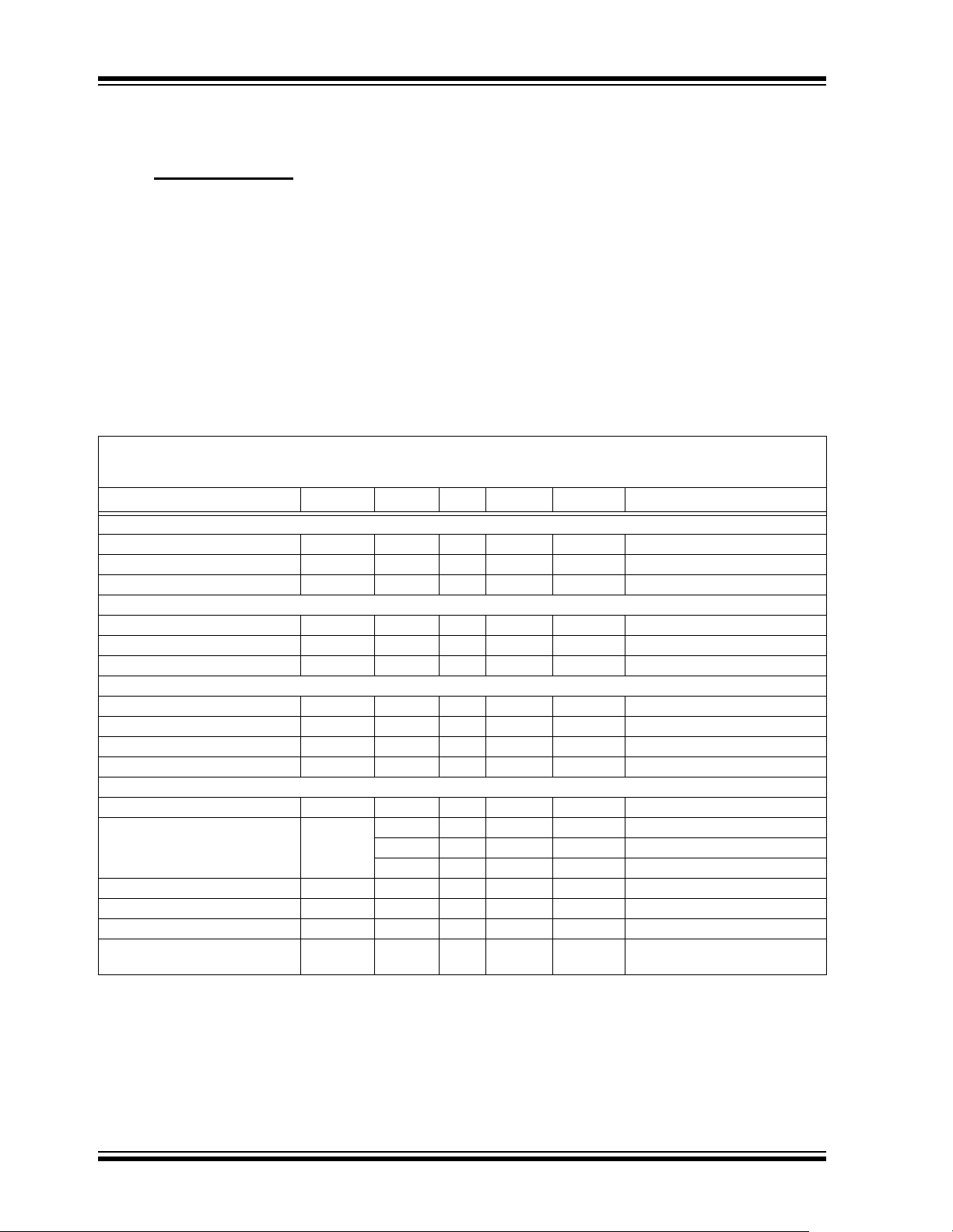
DC CHARACTERISTICS
Electrical Specifications: Unless otherwise indicated, all parameters apply at -40°C ≤ TA ≤ +85°C, VDD = 2.7V or 5.0V.
V
= 2.5V. VIN+ = VIN- = VCM = V
REF
applies to entire MCP3550/1/3 family.
Parameters Sym Min Typ Max Units Conditions
Noise Performance (MCP3550/1)
No Missing Codes NMC 22 — — bits At DC (Note 5)
Output Noise e
Effective Resolution ER — 21.9 — bits RMS V
Noise Performance (MCP3553)
No Missing Codes NMC 20 — — bits At DC (Note 5)
Output Noise e
Effective Resolution ER — 20.6 — bits RMS V
Conversion Times
MCP3550-50 t
MCP3550-60 t
MCP3551 t
MCP3553 t
Accuracy
Integral Non-Linearity INL — ±2 6 ppm T
Offset Error V
Positive Full-Scale Error V
Negative Full-Scale Error V
Offset Drift — 0.040 — ppm/°C
Positive/Negative Full-Scale Error
Drift
Note 1: This parameter is established by characterization and not 100% tested.
2: INL is the difference between the endpoints line and the measured code at the center of the quantization band.
3: This current is due to the leakage current and the current due to the offset voltage between V
4: Input impedance is inversely proportional to clock frequency; typical values are for the MCP3550/1 device. V
5: Characterized by design, but not tested.
6: Rejection performance depends on internal oscillator accuracy; see Section 4.0 “Device Overview” for more informa-
tion on oscillator and digital filter design. MCP3550/1 device rejection specifications characterized from 49 to 61 Hz.
/2. All ppm units use 2*V
REF
N
N
CONV
CONV
CONV
CONV
OS
—2.5— µV
—6—µV
-1.0% 80 +1.0% ms
-1.0% 66.67 +1.0% ms
-1.0% 72.73 +1.0% ms
-1.0% 16.67 +1.0% ms
-12 ±3 +12 µV TA = +25°C
—±4— µVT
—±6— µVT
FS,P
FS,N
-10 ±2 +10 ppm TA = +25°C only
-10 ±2 +10 ppm TA = +25°C only
— 0.028 — ppm/°C
as full-scale range. Unless otherwise noted, specification
REF
RMS
= 5V
REF
RMS
= 5V
REF
= +25°C only (Note 2)
A
= +85°C
A
= +125°C
A
+ and VIN-.
IN
REF
=5V.
DS21950D-page 2 © 2007 Microchip Technology Inc.
Page 3
MCP3550/1/3
DC CHARACTERISTICS (CONTINUED)
Electrical Specifications: Unless otherwise indicated, all parameters apply at -40°C ≤ TA ≤ +85°C, VDD = 2.7V or 5.0V.
= 2.5V. VIN+ = VIN- = VCM = V
V
REF
applies to entire MCP3550/1/3 family.
Parameters Sym Min Typ Max Units Conditions
Rejection Performance
(1,6)
Common Mode DC Rejection — -135 — dB VCM range from 0 to V
Power Supply DC Rejection — -115 — dB
Common Mode 50/60 Hz Rejection CMRR — -135 — dB V
Power Supply 50/60 Hz Rejection PSRR — -85 — dB MCP3551 only, VDD varies from
Power Supply 50/60 Hz Rejection PSRR — -120 — dB MCP3550-50 or MCP3550-60 only
Normal Mode 50 and 60 Hz
Rejection
Normal Mode 50 or 60 Hz
Rejection
Analog Inputs
Differential Input Range V
Absolute/Common Mode Voltages V
Analog Input Sampling Capacitor — 10 — pF Note 5
Differential Input Impedance — 2.4 — MΩ
Shutdown Mode Leakage Current — 1 — nA V
Reference Input
Voltage Range 0.1 — V
Reference Input Sampling
Capacitor
Reference Input Impedance — 2.4 — MΩ Note 4
Shutdown Mode Reference
Leakage Current
Power Requirements
Power Supply Voltage Range V
MCP3550-50, MCP3551 Supply
Current
MCP3550-60, MCP3553 Supply
Current
Supply Current, Sleep Mode I
Supply Current, Shutdown Mode I
Serial Interface
Voltage Input High (CS
Voltage Input Low (CS
, SCK) V
, SCK) V
Voltage Output High (SDO/RDY
Note 1: This parameter is established by characterization and not 100% tested.
2: INL is the difference between the endpoints line and the measured code at the center of the quantization band.
3: This current is due to the leakage current and the current due to the offset voltage between V
4: Input impedance is inversely proportional to clock frequency; typical values are for the MCP3550/1 device. V
5: Characterized by design, but not tested.
6: Rejection performance depends on internal oscillator accuracy; see Section 4.0 “Device Overview” for more informa-
tion on oscillator and digital filter design. MCP3550/1 device rejection specifications characterized from 49 to 61 Hz.
/2. All ppm units use 2*V
REF
as full-scale range. Unless otherwise noted, specification
REF
varies from 0V to V
CM
4.5V to 5.5V
at 50 or 60 Hz respectively, V
varies from 4.5V to 5.5V
NMRR — -85 — dB MCP3551 only,
< VDD,
0 < V
CM
< V
-V
REF
IN
= (V
IN
NMRR — -120 — dB MCP3550-50 or MCP3550-60 only
at 50 or 60 Hz respectively,
< VDD,
0 < V
CM
-V
< V
IN
= (V
IN
IN+
− V
IN-
-V
REF
- 0.3 — V
SS
—+V
REF
+ 0.3 V
DD
REF
V
+ = VIN- = VDD; CS = V
IN
(Note 3)
V
DD
—15— pFNote 5
+ = VIN- = VSS; CS = V
IN
= 2.7V
DD
= 2.7V
DD
DD
+ and VIN-.
IN
DD
I
DD
I
DD
DDSL
DDS
IH
IL
)VOHV
—1— nAV
2.7 — 5.5 V
— 120 170 µA VDD = 5V
— 100 — µA V
— 140 185 µA VDD = 5V
— 120 — µA V
—10 µA
—— 1 µACS = SCK = V
0.7 V
—— V
DD
——0.4 V
- 0.5 — — V VOH = 1 mA, VDD = 5.0V
DD
DD
DD
+ -VIN-) < +V
+ -VIN-) < +V
DD
DD
=5V.
REF
DD
REF
REF
© 2007 Microchip Technology Inc. DS21950D-page 3
Page 4
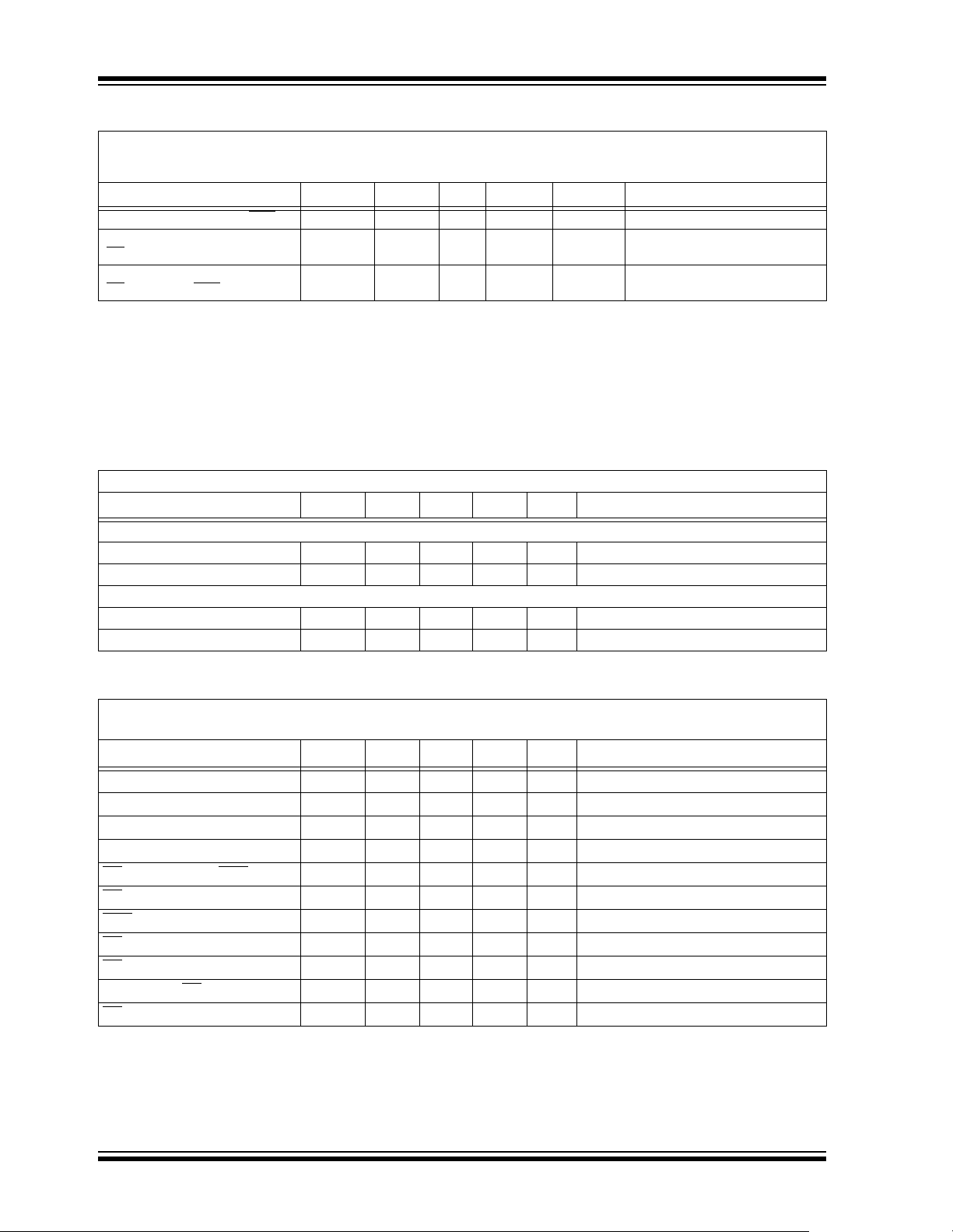
MCP3550/1/3
DC CHARACTERISTICS (CONTINUED)
Electrical Specifications: Unless otherwise indicated, all parameters apply at -40°C ≤ TA ≤ +85°C, VDD = 2.7V or 5.0V.
= 2.5V. VIN+ = VIN- = VCM = V
V
REF
applies to entire MCP3550/1/3 family.
Parameters Sym Min Typ Max Units Conditions
Voltage Output Low (SDO/RDY
Input leakage Current
, SCK)
(CS
Internal Pin Capacitance
, SCK, SDO/RDY)
(CS
Note 1: This parameter is established by characterization and not 100% tested.
2: INL is the difference between the endpoints line and the measured code at the center of the quantization band.
3: This current is due to the leakage current and the current due to the offset voltage between V
4: Input impedance is inversely proportional to clock frequency; typical values are for the MCP3550/1 device. V
5: Characterized by design, but not tested.
6: Rejection performance depends on internal oscillator accuracy; see Section 4.0 “Device Overview” for more informa-
tion on oscillator and digital filter design. MCP3550/1 device rejection specifications characterized from 49 to 61 Hz.
TEMPERATURE CHAR ACTERISTICS
Electrical Specifications: Unless otherwise indicated
Parameters Sym Min Typ Max Units Conditions
Temperature Ranges
Specified Temperature Range T
Operating Temperature Range T
Thermal Package Resistances
Thermal Resistance, 8L-MSOP θ
Thermal Resistance, 8L-SOIC θ
/2. All ppm units use 2*V
REF
)VOL——0.4 VVOH = -1 mA, VDD = 5.0V
I
LI
C
INT
A
A
JA
JA
-1 — 1 µA
—5— pFNote 1
-40 — +85 °C
-40 — +125 °C
—206—°C/W
—163—°C/W
as full-scale range. Unless otherwise noted, specification
REF
+ and VIN-.
IN
REF
=5V.
SERIAL TIMINGS
Electrical Specifications: Unless otherwise indicated, all parameters apply at -40°C ≤ TA ≤ +85°C,
V
= 3.3V or 5.0V, SDO load = 50 pF.
DD
Parameters Sym Min Typ Max Units Conditions
CLK Frequency f
CLK High t
CLK Low t
CLK fall to output data valid t
low to indicate RDY state t
CS
minimum low time t
CS
flag setup time t
RDY
rise to output disable t
CS
disable time t
CS
Power-up to CS
High to Shutdown Mode t
CS
LOW t
CSHSD
SCK
HI
LO
DO
RDY
CSL
SU
DIS
CSD
PUCSL
—— 5MHz
90 — — ns
90 — — ns
0 — 90 ns
0 — 50 ns
50 — — ns
20 — — ns
20 — — ns
90 — — ns
—10—µs
—10—µs
DS21950D-page 4 © 2007 Microchip Technology Inc.
Page 5
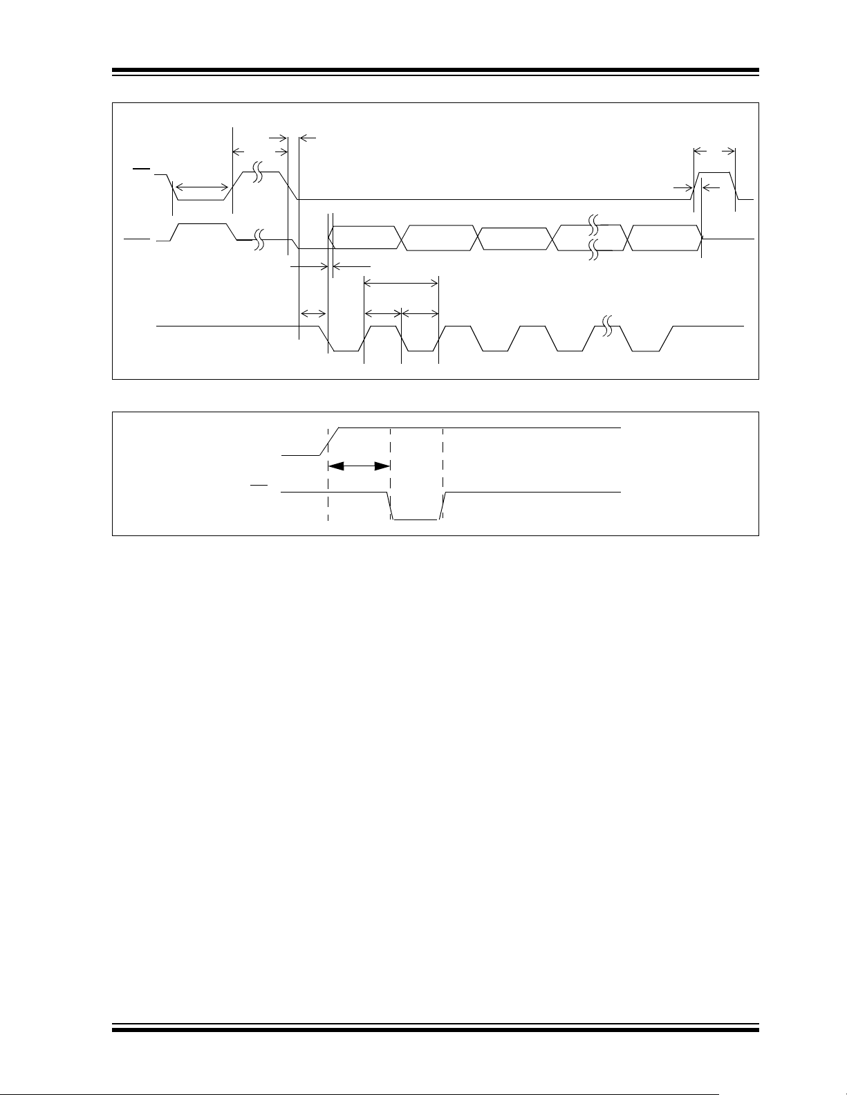
t
RDY
t
CSD
t
CS
CSL
SDO
/RDY
t
DO
t
SCK
SU
FIGURE 1-1: Serial Timing.
V
DD
t
PUCSL
f
SCK
t
HItLO
MCP3550/1/3
t
CSHSD
t
DIS
CS
FIGURE 1-2: Power-up Timing.
© 2007 Microchip Technology Inc. DS21950D-page 5
Page 6
MCP3550/1/3
2.0 TYPICAL PERFORMANCE CURVES
Note: The graphs and ta ble s prov id ed following this n ote are a statistical summ ary based on a l imite d number of
samples and are provided for informational purposes only. The performance characteristics listed herein
are not tested or guaranteed. In some graphs or tables, the data presented may be outside the specified
operating range (e.g., outside specified power supply range) and therefore outside the warranted range.
Note: Unless otherwise specified, TA = +25°C, VDD = 5V, V
All ppm units use 2*V
5
4
3
2
1
0
-1
INL (ppm)
-2
-3
-4
-5
-2.5 -1.5 -0.5 0.5 1.5 2.5
as full-scale range. Unless otherwise noted, graphs apply to entire MC P35 50 /1/3 famil y.
REF
+125 C
+85 C
-40 C
+25 C
V
(V)
IN
FIGURE 2-1: INL Error vs. Input Voltage
(V
= 2.7V).
DD
5
4
3
2
1
0
-1
INL (ppm)
-2
-3
-4
-5
-2.5 -1.5 -0.5 0.5 1.5 2.5
+125 C
+85 C
V
- 40 C
+25 C
(V)
IN
= 2.5V, VSS = 0V, VCM = V
REF
10
8
6
4
INL Error (ppm)
2
0
00.511.522.533.544.55
/2, VIN+ = VIN-.
REF
V
(V)
REF
FIGURE 2-4: Maximum INL Error vs.
V
.
REF
10
9
8
7
6
5
4
3
Max INL (ppm)
2
1
0
-50 -25 0 25 50 75 100 125
Temperature (°C)
FIGURE 2-2: INL Error vs. Input Voltage
= 5.0V).
(V
DD
10
8
6
4
2
0
-2
INL (ppm)
-4
-6
-8
-10
-5 -4 -3 -2 -1 0 1 2 3 4 5
+125 C
+85 C
+25 C
-40 C
V
(V)
IN
FIGURE 2-3: INL Error vs. Input Voltage
(V
DD
= 5.0V, V
REF
= 5V).
FIGURE 2-5: Maximum INL Error vs.
Temperature.
10
)
9
RMS
8
7
6
5
4
3
2
Output Noise (µV
1
0
-2.5 -1.5 -0.5 0.5 1.5 2.5
MCP3553
MCP3550/1
(Volts)
V
IN
FIGURE 2-6: Output Noise vs. Input
Voltage (V
= 2.7V).
DD
DS21950D-page 6 © 2007 Microchip Technology Inc.
Page 7
MCP3550/1/3
MCP3550/1
MCP3550/1
Note: Unless otherwise specified, TA = +25°C, VDD = 5V, V
All ppm units use 2*V
15
)
RMS
10
5
Output Noise (µV
0
-2.5 -1.5 -0.5 0.5 1.5 2.5
as full-scale range. Unless otherwise noted, graphs apply to entire MCP3550/1/3 family.
REF
MCP3553
MCP3550/1
V
(V)
IN
FIGURE 2-7: Output Noise vs. Input
Voltage (V
u
10.0
9.0
)
8.0
RMS
7.0
6.0
5.0
4.0
3.0
2.0
Output Noise (µV
1.0
0.0
= 5.0V).
DD
MCP3553
0.0 1.0 2.0 3.0 4.0 5.0
V
(V)
REF
= 2.5V, VSS = 0V, VCM = V
REF
10
9
)
8
RMS
7
6
5
4
3
2
Output Noise (µV
1
0
-50-250 255075100125
Temperature (°C)
/2, VIN+ = VIN-.
REF
MCP3553
FIGURE 2-10: Output Noise vs.
Temperature.
5
4
3
2
Offset (µV)
1
0
2.533.544.555.5
(V)
V
DD
MCP3550/1
FIGURE 2-8: Output Noise vs. V
10
)
9
8
RMS
7
6
5
4
3
2
Output Noise (µV
1
0
2.533.544.555.5
MCP3553
V
(V)
DD
FIGURE 2-9: Output Noise vs.V
REF
DD
.
.
FIGURE 2-11: Offset Error vs V
(V
=0V).
CM
7
6
5
4
3
Offset (µV)
2
1
0
-50 -25 0 25 50 75 100 125
Temperature (°C)
FIGURE 2-12: Offset Error vs.
Temperature (V
REF
= 5.0V).
DD
© 2007 Microchip Technology Inc. DS21950D-page 7
Page 8

MCP3550/1/3
consecutive
16384 consecutive
Note: Unless otherwise specified, TA = +25°C, VDD = 5V, V
All ppm units are ratioed against 2*V
5
4
3
2
1
0
-1
-2
-3
Full-Scale Error (ppm)
-4
-5
2.533.544.555.5
Positive Full-Scale
Negative Full-Scale
V
(V)
DD
Unless otherwise noted, graphs apply to entire MCP3550/1/3 family.
REF .
FIGURE 2-13: Full-Scale Error vs. VDD.
10
8
6
4
2
0
-2
-4
-6
Full-Scale Error (ppm)
-8
-10
-50 -25 0 25 50 75 100 125
Positive Full-Scale
Negative Full -S c a le
Temperature (°C)
= 2.5V, VSS = 0V, VCM = V
REF
4000
V
= 5V
3500
3000
2500
2000
1500
DD
V
= 2.5V
REF
V
= 1.25V
CM
V
= 0V
IN
T
= 25C
A
16384
readings
/2, VIN+ = VIN-.
REF
1000
500
Number of Occurrences
0
-15 -10 -5 0 5 10 15
Output Code (LSB)
FIGURE 2-16: MCP3550/1 Output Noise
Histogram.
1800
V
= 5V
DD
1600
V
= 2.5V
REF
V
= 1.25V
CM
1400
V
= 0V
IN
1200
T
= 25°C
A
1000
readings
800
600
400
200
Number of Occurrences
0
-15 -10 -5 0 5 10 15
Output Code (LSB)
FIGURE 2-14: Full-Scale Error vs.
Temperature.
10
8
6
4
Positive Full-Scale
2
0
-2
-4
-6
Full-Scale Error (ppm)
-8
Negative Full-Scale
-10
-50 -25 0 25 50 75 100 125
Temperature (°C)
FIGURE 2-15: Full-Scale Error vs.
Temperature (V
REF
= 5.0V).
FIGURE 2-17: MCP3553 Output Noise
Histogram.
5.0
4.0
3.0
2.0
1.0
0.0
-1.0
TUE (ppm)
-2.0
-3.0
-4.0
-5.0
-2.5 -2.0 -1.5 -1.0 -0.5 0.0 0.5 1.0 1.5 2.0 2.5
(V)
V
IN
FIGURE 2-18: Total Unadjusted Error
(TUE) vs. Input Voltage (VDD = 2.7V).
DS21950D-page 8 © 2007 Microchip Technology Inc.
Page 9

MCP3550/1/3
Note: Unless otherwise specified, TA = +25°C, VDD = 5V, V
All ppm units use 2*V
5
4
3
2
1
0
-1
TUE (ppm)
-2
-3
-4
-5
-2.5 -2 -1.5 -1 -0.5 0 0.5 1 1.5 2 2.5
as full-scale range.
REF
(V)
V
IN
Unless otherwise noted, graphs apply to enti re M CP355 0/1/3 family.
FIGURE 2-19: Total Unadjusted Error
(TUE) vs. Input Voltage.
10
8
6
4
2
0
-2
TUE (ppm)
-4
-6
-8
-10
-5-4-3-2-1012345
V
(V)
IN
= 2.5V, VSS = 0V, VCM = V
REF
6
5
4
3
2
1
Maximum TUE (ppm)
0
-50 -25 0 25 50 75 100 125
Temperature (°C)
/2, VIN+ = VIN-.
REF
FIGURE 2-22: Maximum TUE vs.
Temperature.
5
4.5
4
3.5
3
2.5
2
TUE (ppm)
1.5
1
0.5
0
2.5 2.7 3 3.3 4 5 5.5
V
(V)
DD
FIGURE 2-20: Total Unadjusted Error
(TUE) vs. Input Voltage (V
10
9
8
7
6
5
4
3
2
Maximum TUE (ppm)
1
0
012345
FIGURE 2-21: Maximum TUE vs. V
V
REF
REF
(V)
= 5.0V).
REF
FIGURE 2-23: Maximum TUE vs. V
0.6
0.5
0.4
0.3
(µA)
0.2
DDS
I
0.1
0
-0.1
-50-25 0 255075100125
.
FIGURE 2-24: I
MCP3550/1
MCP3553
Temperatur e ( °C)
vs. Temperature.
DDS
DD
.
© 2007 Microchip Technology Inc. DS21950D-page 9
Page 10

MCP3550/1/3
Note: Unless otherwise specified, TA = +25°C, VDD = 5V, V
All ppm units use 2*V
200
180
160
140
120
100
(µA)
DD
80
I
60
40
20
MCP3550-60, MCP3553
0
2.5 3 3.5 4 4.5 5 5.5
as full-scale range. Unless otherwise noted, graphs apply to entire MC P35 50 /1/3 famil y.
REF
MCP3550-50, MCP3550/1
(V)
V
DD
= 2.5V, VSS = 0V, VCM = V
REF
160
MCP3550-60, MCP3553
140
120
100
80
(µA)
DD
I
60
40
20
0
-50 -25 0 25 50 75 100 125
/2, VIN+ = VIN-.
REF
MCP3550-50, MCP3550/1
Temperature (°C)
FIGURE 2-25: IDD vs. VDD. FIGURE 2-26: IDD vs. Temperature.
DS21950D-page 10 © 2007 Microchip Technology Inc.
Page 11

3.0 PIN DESCRIPT IONS
TABLE 3-1: PIN FUNCTION TABLE
Pin No. Symbol I/O/P Function
1V
2V
3V
4V
5 SCK I Serial Clock Digital Input Pin
6 SDO/RDY
7CS
8V
Type Identification: I = Input; O = Output; P = Power
REF
+ I Non-inverting Analog Input Pin
IN
- I Inverting Analog Input Pin
IN
SS
DD
I Reference Voltage Analog Input Pin
P Ground Pin
O Data/Ready Digital Output Pin
I Chip Select Digital Input Pin
P Positive S upply Voltage Pin
MCP3550/1/3
3.1 Voltage Reference (V
The MCP3550/1/3 devices accept single-ended reference voltages from 0.1V to V
output noise is dominated by thermal noise, which is
independent of the reference voltage, the output noise
is not significantly improved by diminishing the reference voltage at th e V
reference will significantly improve the INL performance (see Figure 2-4); the INL max error is
proportional to V
REF
input pin. A reduced voltage
REF
2
.
. Since the converter
DD
REF
)
3.2 Analog Inputs (VIN+, VIN-)
The MCP3550/1/3 devices accept a fully differential
analog input voltage to be connected on the V
V
- input pins. The differential voltage that is con-
IN
verted is defined by V
voltage range specified for ensured accuracy is from
-V
to +V
REF
valid and usable codes with the inputs overranged by
up to 12% (see Section 5.0 “Serial Interface”) at
room temperature. This overrange is clearly specified
by two overload bits in the output code.
The absolute voltage range on these input pins extends
from V
SS
below this range will create leak age currents through
the Electrostatic Discharge (ESD) diodes. T his current
will increase exponentially, degrading the accuracy and
noise performance of the device. The common mode of
the analog inputs should be chose n such that both the
differential analog input range and the absolute voltage
range on each pin are within the specified operating
range defined in Section 1.0 “Electrical Characteris-
tics”.
. However, the converter will still output
REF
– 0.3V to VDD + 0.3V. Any voltage above or
= VIN+ – VIN-. The diffe ren tial
IN
+ and
IN
3.3 Supply Voltage (VDD, VSS)
VDD is the power supply pin for the analog and digital
circuitry within the MCP3550/1/3. This pin requires an
appropriate bypass capacitor of 0.1 µF. The voltage on
this pin should be maint ain ed in th e 2.7V to 5.5 V range
for specified operation. V
current return path for both analog and digital circuitry
of the MCP3550/1/3. If an analog ground plane is
available, it is recommended that this device be tied to
the analog ground plane of the Printed Circuit Board
(PCB).
is the ground pin and the
SS
3.4 Serial Clock (SCK)
SCK synchronizes data communication with the
device. The device operates in both SPI mode 1,1 and
SPI mode 0,0. D ata is shif ted o ut of the device on the
falling edge of SCK. Data is latched in on the rising
edge of SCK. During CS
idle either high or low.
high times, the SCK pin can
3.5 Data Output (SDO/RDY)
SDO/RDY is the output data pin for the device. Once a
conversion is complete, this pin will go active-low,
acting as a ready flag. Subsequent falling clock edges
will then place the 24-bit data word (two overflow bits
and 22 bits of data, see Section 5.0 “Serial Inter-
face”) on the SPI bus through the SDO pin. Data is
clocked out on the falling edge of SCK.
3.6 Chip Select (CS)
CS gates all communication to the device and can be
used to select multiple devices that share the same
SCK and SDO/RDY
control the internal conversions, which begin on the
falling edge of CS. Raising CS before the first internal
conversion is complete places the device in Single
Conversion mode. Leaving CS
device in Continuo us Co nversion mode (i .e., additi onal
internal conv ersi ons will au toma tically occur) . CS
be tied permanently low for two-wire Continuous
Conversion mode op erati on. SDO/ RDY
impedance state with CS
pins. This pin is also used to
low will place the
may
enters a high-
high.
© 2007 Microchip Technology Inc. DS21950D-page 11
Page 12

MCP3550/1/3
4.0 DEVICE OVERVIEW
The MCP3550/1/3 devices are 22-bit delta-sigma
ADCs that include fully differential analog inputs, a
third-order delta-sigma modulator, a fourth-order
modified SI NC deci mation filter, an on- chip, low-noi se
internal oscilla tor , a power supp ly monitorin g circuit and
an SPI 3-wire digital interface. These devices can be
easily used to measure low-frequency, low-level
signals such as those found in pressure transducers,
temperature, strai n ga uge, i ndust rial c ontrol or p roces s
control applications. The power supply range for this
product family is 2.7V to 5 .5V ; the temperatu re range i s
-40°C to +125°C. The functional block diagram for the
MCP3550/1/3 devices is shown in Figure 4-1.
A Power-On Reset (POR) monitoring circuit is incl uded
to ensure proper power supply voltages during the
conversion process. The clock source for the part is
internally generated to ±0.5% over the full-power
supply voltage range and in dustrial tempe ratu re rang e.
This stable clock source allows for superior conversion
repeatability and minimal drift across conversions.
The MCP3550/1/3 devices employ a delta-sigma
conversion technique to realize up to 22 bits of no
missing code per f or ma nc e wit h 21 . 9 Effec tiv e Num be r
of Bits (ENOB). These devices provide single-cycle
conversions with no digital filter settling time. Every
conversion includes an internal offset and gain autocalibration to reduce device error. These calibrations
are transparent to the user and are done in real-time
during the conversi on. There fore, t hese de vice s do not
require any additional time or conversion to proceed,
allowing easy usage of the devices for multiplexed
applications. The MCP3550/1/3 devices incorporate a
fourth-order digital decimation filter in order to allow
superior averaging performance, as well as excellent
line frequency rejection capabilities. The oversampling
frequency also reduces any external anti-aliasing filter
requirements.
The MCP3550/1/3 device s communicate with a sim pl e
3-wire SPI interface. The interface controls the
conversion start event, with an added feature of an
auto-conversion at system power-up by tying the CS
pin to logic-low. The device can communicate with bus
speeds of up to 5 MHz, with 50 pF capacitive loading.
The interface offers two conversion modes: Single
Conversion mode for multiplexed applications and a
Continuous Conversion mode for multiple conversions
in series. Every conversion is independent of each
other . That is, all i nternal regis ter s are flushed betw een
conversions. When the de vice is not convert ing, it automatically goes into Shutdown mode and, while in this
mode, consumes less than 1 µA.
Reference
Input
Differential
Analog Input
Gain and
Offset
Calibration
Charge
Transfer
Third-Order
ΔΣ
Modulator
Clock
Internal
Oscillator
Bit
Stream
Digital
Decimation
Filter (SINC
Conversion
4
)
Code
SPI 3-wire
Interface
Output
Code
FIGURE 4-1: MCP3550/1/3 Functional Block Diagram.
DS21950D-page 12 © 2007 Microchip Technology Inc.
Page 13

MCP3550/1/3
4.1 MCP3550/1/3 Delt a-Sigma Modulator with Internal Offset and Gain Calibration
The converter core of the MCP3550/1/3 devices is a
third-order delta-sigma modulator with automatic gain
and offset error cal ibrations. The mo dulator uses a 1-b it
DAC structure. The delta-sigma modulator processes
the sampled charges through switched capacitor
structures controlled by a very low drift oscillator for
reduced clock jitter.
During the conversion process, the modulator outputs
a bit stream with the bit frequency equivalent to the
/4 (see Table 4-1). The high oversampling
f
OSC
implemented in the modulator ensures very high
resolution and high averaging factor to achieve lownoise specifications. The bit stream output of the modulator is then processed by the digital decimation filter
in order to provide a 22-bit outp ut code at a da ta rate of
12.5 Hz for the MCP3550-50, 15 Hz for the MCP3550-
60, 13.75 Hz for the MCP3551 and 60 Hz for the
MCP3553. S ince the overs ampling rat io is lower with
the MCP3553 device, a mu ch higher output da ta rate is
achieved while still ac hieving 20 bit s No M issing Codes
(NMC) and 20.6 ENOB.
A self-calibration of offset and gain occurs at the onset
of every conversion. The conversion data available at
the output of the device is always calibrated for offset
and gain through this process. This offset and gain
auto-calibration is performed internally and has no
impact on the speed of the converter since the offset
and gain errors are calibrated in real-time during the
conversion. The real-time offset and gain calibration
schemes do not affect the conversion process.
4.2 Digital Filter
The MCP3550/1/3 devices include a digital decimation
filter, which is a fourth-order modified SINC filter. This
filter averages the incoming bit stream from the modulator and outputs a 22-bit conversion word in binary
two's complement. When all bits have been processed
by the filter, the output code is ready for SPI communication, the RDY
the internal registers are reset in order to process the
next conversion.
Like the common ly use d SINC fi lter, the modified SINC
filter in the MCP3550/1/3 family has the main notch
frequency located at f
stream sample frequency. OSR is the Oversampling
Ratio and L is the order of the filter.
The MCP3550-50 device has the main filter notch
located at 50 Hz. For the MCP3550-60 device, the
notch is located at 60Hz. The MCP3551 device has it s
notch located at 55 Hz, and for the MCP3553 device,
the main notch is located at 240 Hz, with an OSR of
128. (see Table 4-1 for rejection performance).
The digital decimation SINC filter has been modified in
order to offer staggered zeros in its transfer function.
This modification i s intended to widen the main notch i n
order to be less sensitive to oscillator deviation or linefrequency drift. The MCP3551 filter has staggered
zeros spread in order to reject both 50 Hz and 60 Hz
line frequencies simultaneously (see Figure 4-2).
flag is set on the SDO/RDY pin and all
/(OSR*L), where fS is the bit
S
T ABLE 4-1: DATA RATE, OUTPUT NOISE AND DIGITAL FILTER SPECIFICATIONS BY DEVICE
Output Data
Device
MCP3550-50 80.00 ms 2.5 50 25600 Hz 102.4 kHz -120 dB min. at
MCP3550-60 66.67 ms 2.5 60 30720 Hz 122.88 kHz -120 dB min. at
MCP3551 72.73 ms 2.5 55 28160 Hz 112.64 kHz -82 dB min. from
MCP3553 16.67 ms 6 240 30720 Hz 122.88 kHz Not Applicable
Note: For the first conversion after exiting Shutdown, t
the conversion is complete and the RDY
© 2007 Microchip Technology Inc. DS21950D-page 13
Rate (t
(Note)
CONV
)
Output
Noise
(µV
Primary
Notch
)
RMS
(Ready) flag appears on SDO/RDY.
(Hz)
CONV
Sample
Frequency
(fS)
must include an additional 144 f
Internal
Clock
f
OSC
50/60 Hz Rejection
50 Hz
60 Hz
48 Hz to 63 Hz. -
82 dB at 50 Hz and
-88 dB at 60 Hz
periods before
OSC
Page 14

MCP3550/1/3
:
0
-20
-40
-60
-80
Attenuation (dB)
-100
-120
0 50 100 150 200
Frequency (Hz)
0
-20
-40
-60
-80
-100
Normal Mode Rejection (dB)
-120
-140
0 28160 56320 84480 112640 140800 168960 197120 225280 253440
Frequency (Hz)
FIGURE 4-2: SINC Filter Response,
MCP3550-50 Device.
:
0
-20
-40
-60
-80
Attenuation (dB)
-100
-120
0 60 120 180 240
Frequency (Hz)
FIGURE 4-3: SINC Filter Response,
MCP3550-60 Device.
:
0
-10
-20
-30
-40
-50
-60
-70
-80
-90
Attenuation (dB)
-100
-110
-120
0 102030405060708090100110
Frequency (Hz)
FIGURE 4-4: SINC Filter Response,
MCP3551 Device, Simultaneous 50/60 Hz
Rejection.
FIGURE 4-5: SINC Filter Response at
Integer Multiples of the Sampling Frequency (f
s
4.3 Internal Oscillator
The MCP3550/1/3 devices include a highly stable and
accurate internal oscillator that provides clock signals
to the delta-s igma A DC with minimu m jitte r. The oscillator is a spec ialized st ructure wit h a low temp erature
coefficient across the full range of specified operation.
See Table 4-1 for oscillator frequencies.
The conversion time is an integer multiple of the internal clock period and, th erefore, has the same accu racy
as the internal clock frequency. The internal oscillator
frequency is 102.4kHz ±1% for the MCP3550-50,
112.64 kHz ±1% for the MCP3551, and 122.88 kHz
±1% for the MCP3550-60 and MCP3553 devices,
across the full power supply voltage and specified
temperature ranges.
The notch of the digital filter is proportional to the
internal oscillator frequency, with the exact notch
frequency equivalent to the oscillator accuracy (< 1%
deviation). This high accuracy, combined with wide
notches, will ensure tha t the MCP3551 will hav e simu ltaneous 50 Hz and 60 Hz line frequency rejection and
the MCP3550-50 or MCP3550-60 devices will have
greater than 120 dB rejection (at either 50 or 60 Hz) by
the digital filtering, even when jitter is present.
The internal oscillator is held in the reset condition
when the par t is in Shutdown mode to ensure very low
power consumption (< 1µA in Shutdown mode). The
internal oscillator is independent of all serial digital
interface edges (i.e., state machine processing the
digital SPI in terface is asy nchronous w ith respect to the
internal clock edges).
).
DS21950D-page 14 © 2007 Microchip Technology Inc.
Page 15

MCP3550/1/3
4.4 Differential Analog Inpu ts
The MCP3550/1/3 devices accept a fully differential
analog input voltage to be connected to the V
input pins. The differential voltage that is converted
V
IN-
is defined by V
= VIN+ – VIN-. The differen tia l vol tage
IN
range specified for ensured accuracy is from -V
.
+V
REF
The converter will outp ut valid an d usabl e code s from 112% to 112% of output range (see Section 5.0
“Serial Interface”) at room temperature. The ±12%
overrange is clearly specified by two overload bits in
the output code: O VH an d O V L . Th is fe ature a llo w s for
system calibration of a positive gain error.
The absolute volt age range on th ese input pins ext ends
from V
- 0.3V to V
SS
+ 0.3V. If the input voltages are
DD
above or below this range, the leakage currents of the
ESD diodes will increase exponentially, degrading the
accuracy and noise performance of the converter. The
common mode of the analog inputs should be chosen
such that both the differential analog input range and
absolute voltage range on each pin are within the
specified operating range defined in Section 1.0
“Electrical Characte ristics”.
Both the analog differential inputs and the reference
input have switched-capacitor input structures. The
input capacit ors are charged a nd discharged a lternatively with the input and the reference in order to
process a conversi on. The charg e and discharge of the
input capacitors create dynamic input currents at the
+ and VIN- input pins inversely proportional to the
V
IN
sampling capacitor. This current is a function of the
differential input voltages and their respective common
modes. The typical va lue of the differenti al input impedance is 2.4 MΩ, with V
= 2.5V , V
CM
DD
= V
REF
DC leakage current caused by the ESD input diodes,
even though on the ord er of 1nA, can cause additional
offset errors proporti onal to the source resi stance at the
+ and VIN- input pins .
V
IN
From a transient response standpoint and as a firstorder approximation, these input structures form a
simple RC filtering c ircui t with the sour ce imped an ce in
series with the R
(switched resist anc e when closed)
ON
of the input switc h a nd the sampling capac ito r. In order
to ensure the accuracy of the sampled charge, proper
settling time of the input circuit has to be considered.
Slow settling of the input circuit will create additional
gain error. As a rule of thumb, in order to obtain 1 ppm
absolute measurement accuracy, the sampling period
must be 14 time s g rea ter than the input ci rcu it RC tim e
constant.
and
IN+
to
REF
= 5V . The
4.5 Voltage Reference Input Pin
The MCP3550/1/3 devices accept a single-ended
external reference voltage, to be connected on the
input pin. Internally, the reference voltage for the
V
REF
ADC is a differential voltage with the non-inverting input
connected to the V
connected to the V
voltage is V
REF - VSS
reference is always (V
pin and the inverting input
REF
pin. The value of the reference
SS
and the common mode of the
- VSS)/2.
REF
The MCP3550/1/3 devices accept a single-ended
reference voltage from 0.1V to V
The converter
DD.
output noise is dominated by thermal noise that is
independent of the reference voltage. Therefore, the
output noise is not significantly improved by lowering
the reference volta ge at the V
input pin. However, a
REF
reduced reference v olt age will signi ficant ly im prove th e
INL performance since the INL max error is
proportional to V
2
(see Figure 2-4).
REF
The charge and discha rge of the input c apa citor c reate
dynamic input currents at the V
input pin inversely
REF
proportional to the sampling capacitor, which is a function of the input reference voltage. The typical value of
the single-ended input impedance is 2.4 MΩ, with
V
DD=VREF
= 5V. The DC leakage current caused by
the ESD input diodes, though on the order of 1 nA
typically , can cause additi onal gain error pr oportional to
the source resistance at the V
REF
pin.
4.6 Power-On Reset (POR)
The MCP3550/1/3 devices contain an internal PowerOn Reset (POR) circuit that monitors power supply
voltage VDD during operation. This circuit ensures
correct device start-u p at syste m power-up and pow erdown events. The POR has built-in hysteresis and a
timer to give a high degree of immunity to potential
ripple and noise on the power supplies, as well as to
allow proper settlin g of the p ower sup ply durin g pow erup. A 0.1 µ F deco upling capacitor should be mounted
as close as possib le to the V
transient immunity.
The threshold v ol t ag e is s et at 2.2V, with a tolerance of
approximately ±5%. If the supply voltage falls below
this threshold, the MCP3550 /1/3 devic es wil l be he ld in
a reset condition or in Shutdown mode. When the part
is in Shutdown mode, the power consumption is less
than 1 µA. The typical hysteresis value is around
200 mV in order to prevent reset during brown-out or
other glitches on the power supply.
pin, providing add itional
DD
© 2007 Microchip Technology Inc. DS21950D-page 15
Page 16

MCP3550/1/3
Once a power-up event has occurred, the device must
require additional time before a conversion can take
place. During this time, all inte rnal analog circ uitry must
settle before the first conversion can occur. An internal
timer counts 32 internal clock periods before the
internal oscillator can provide clock to the conversion
process. This allows all internal analog circuitry to
settle to their proper operating point. This timing is
typically less than 3 00 µs, which is negligible c ompared
to one conversion time (e.g. 72.7ms for the
MCP3551). Figure 4-6 illustrates the conditions for a
power-up and power-down event unde r typica l st art-up
conditions.
V
DD
2.2V
2.0V
300 µs
0V
Reset
Normal
Operation
ResetStart-up
Time
4.8 Sleep Mode
During Sleep mode, the device is not co nv erti ng and i s
awaiting data retrieval; the internal analog circuitry is
still running and the device typically consumes 10 µA.
In order to restart a conversion while in Sleep mode,
toggling CS
down mode) and t hen back t o a logi c-low will restart th e
conversion. Sleep can only be entered in Single
Conversion mode. Once a conversion is complete in
Single Conversion mode, the device automatically
enters Sleep mode.
to a logic-high (placing the part in Shut-
FIGURE 4-6: Power-On Reset Operation.
4.7 Shutdown Mode
When not internally converting, the two modes of
operation for the MCP3550/1/3 devices are
Shutdown and Sleep modes. During Shutdown mode,
all internal analog circui try , including the POR, is turned
off and the device consumes less than 1 µA. When
exiting Shutd own m ode , th e devi ce mu st re qui re ad ditional time before a conversion can take place. During
this time, all internal analog circuitry must settle before
the first conversion can occur. An internal timer counts
32 intern al clock peri ods before th e internal osc illator
can provide clock to the conversion process. This
allows all internal analog circuitry to settle to their
proper operating point. Th is timing is typically less than
300 µs, which is neglig ible comp ared to one con version
time (72.7 ms for MCP3551).
the
DS21950D-page 16 © 2007 Microchip Technology Inc.
Page 17

MCP3550/1/3
5.0 SERIAL INTERFACE
5.1 Overview
Serial communication between the microcontroller and
REF
, SCK
– 1 LSB,
, OVL
REF
the MCP3550/1/3 devices is achieved using CS
and SDO/RDY
. There are two modes of operation:
Single Conversion and Continuous Conversion. CS
controls the conversion start. There are 24 bits in the
data word: 22 bits of conv ers io n dat a and two ov erfl ow
bits. The conversion process takes place via the internal oscillator and the status of this conversion must be
detected. The typical method of communication is
shown in Figure5-1. The status of the internal conversion is the SDO/RDY
A High state on SDO/RDY
pin and is available with CS low.
means the device is busy
converting, while a Low state means the conversion is
finished and data is ready for transfer using SCK.
SDO/RDY
CS
data using SCK and SDO/RDY
Bit 22 is Overflow High (OVH) when V
remains in a high-impedance state when
is held high. CS must be low when cl ock in g o ut the
.
> V
IN
OVH toggles to logic ‘1’, detecting an overflow high in
the analog input voltage.
Bit 23 is Overflow Low (OVL) when V
IN
< -V
toggles to logic ‘1’, detecting an overflow low in the
analog input voltage. The state OVH = OVL = ‘1’ is not
defined an d should be co nsidered as an i nterrupt for
the SPI interface meaning erroneo us co mm uni ca tio n.
Bit 21 to bit 0 represents the output code in 22-bit
binary two's complement. Bit 21 is the sign bit and is
logic ‘0’ when the differential analog input is positive
and logic ‘1’ when the differential analog input is
negative. From Bit 20 to bit 0, the output code is given
MSb first (MSb is bit 20 and LSB is Bit 0). When the
analog input value is comprised between -V
– 1 LSB, the two overflow bits are set to logic ‘0’.
V
REF
REF
and
The relationship between input voltage and output
code is shown in Figure 5-1.
The delta-sigma modulator saturation point for the
differential analog input is located at around ±112% of
(at room temp erat ure), m ean ing that the mo dul a-
V
REF
tor will still give accurate output codes with an overrange of 12% below or above the reference voltage.
Unlike the usual 22-bit device, the 22-bit output code
will not lock at 0x1FFFFF for positive sign inputs or
0x200000 for negative sign inputs in order to take
advantage of the overrange capabilities of the device.
This can be practical for closed-loop operations, for
instance. In case of an overflow, the output code
becomes a 23-bit two's complement output code,
where the sign bit will be the OVL bit. If an overflow high
or low is detected, OVL (bit 23) becomes the sign bit
(instead of bit 21), the MSb is then bit 21 and the converter can be us ed as a 23 - bit t wo' s co mp l em ent co de
converter, with output code from bits B21 to B0, and
OVL as the sign bit. Figure 5 -1 summarizes the output
coding data format with or without overflow high and
low.
CS
SCK
SDO/RDY
READY
DOO
21 20 19 18 17 16 15 14 13 12 11 10 9
HLR
765 4321
8
HI-Z
0
FIGURE 5-1: Typical Serial Device Communication and Example Digital Output Codes for Specific
Analog Input Voltages.
© 2007 Microchip Technology Inc. DS21950D-page 17
Page 18

MCP3550/1/3
5.2 Controlling Internal Conversions and the Internal Oscillator
During Shutdown mode, on the falling edge of CS, the
conversion process begins. During this process, the
internal oscillat or clocks the delt a-sigma m odulator and
the SINC filter until a conversion is complete. This
conversion time is t
Figure 5-2. At the end of t
settled complete ly and the re is no l atency in volved wi th
the digital SINC filter of the MCP3550/1/3.
The two modes of conversion for the MCP3550/1/3
devices are Single Conversion and Continuous
Conversion. In Single C onversi on mo de, a co nsecutiv e
conversion will not au tomatica lly b egin. Instea d, after a
single conversion is complete and all four filters have
settled, the device put s the data into the output regis ter
and enters shutdown.
CS
Int. Osc
and the timing is shown in
CONV
t
CONV
, the digital filter has
CONV
Sleep
In Continuous Conversion mode, a consecutive
conversion will be automatic. In this mode, the device
is continuously converting, independent of the serial
interface. The most recent conversion data will always
be available in the Output regis ter.
When the device exits Shutdown, there is an internal
power-up delay that must be observed.
Shutdown
SCK (opt)
SDO/RDY
Hi-Z
FIGURE 5-2: Single Conversion Mode.
CS
Int. Osc
t
CONV
SCK (opt)
SDO/RDY
t
CONV
t
CONV
x24
Hi-Z
Shutdown
x24
Hi-Z
FIGURE 5-3: Continuous Conversion Mode.
DS21950D-page 18 © 2007 Microchip Technology Inc.
Page 19

MCP3550/1/3
5.3 Single Conversion Mode
If a rising edge of Chip Select (CS) occurs during t
a subsequen t conversion will not take place and the
device will enter low-power Shutdown mode after
completes. This is referred to as Single
t
CONV
Conversion mode. This operation is demonstrated in
Figure 5-3. Note that a falling edge of CS
same conversion that detected a rising edge, as in
Figure 5-2, will not initiate a new conversion. Once a
rising edge is seen, the device will enter Sleep, then
Shutdown mode. Once the device has been put into
Single Conversion m ode, the dat a mus t be clo cked o ut
in order for a new conversion to take place. A
subsequent falling edg e on CS
during Shutdown mode
will not initiate a new conversion, unless the prior
conversion data has been clocked out of the device.
After the final data bit has been c locked out o n the 25th
clock, the SDO/RDY
pin will go active-high.
5.3.1 READY FUNCTION OF SDO/RDY
PIN, SINGLE CONVERSION MODE
At every falling edge of CS during the internal conversion, the state of the internal conversion is latched on
the SDO/RDY pin to give ready or busy information. A
High state means the dev ice is cu rrently performin g an
internal conversion and data cannot be clocked out. A
Low state m eans the device has finished its c onversio n
and the data is read y f or re trieval on the fallin g ed ge of
SCK. This operation is demonstrated in Figure 5-4.
Note that the device has been put into Single
Conversion mode with the first rising edge of CS
Note: The Ready state is latched on each falling
edge of CS
update if CS
and will not dynamically
is held low. CS must be
toggled high through low.
CS
Int. Osc
t
CONV
SDO/RDY
Hi-Z
FIGURE 5-4: RDY Functionality in Single
Conversion Mode.
CONV
during the
.
5.4 Continuous Conversion Mode
,
If no rising edge of CS occurs durin g any given conv ersion per Figure5-2, a subsequent conversion will take
place and the contents of the previous conversion will
be overwritten. This operation is demonstrated in
Figure 5-5. Once conversio n outpu t dat a has s ta rted to
be clocked out, the output buffer is not refreshed until
all 24 bits have been clocked. A complete read must
occur in order to read the ne xt conve rsion in this m ode.
The subsequent conversion d ata to be read wil l then be
the most recent conversion. The conversion time is
fixed and cannot b e shortened by the ris ing edge of CS
This rising edge will place the part in Shutdown mode
and all conversion data will be lost.
The transfer of data from the SINC filter to the output
buffer is demonstrated in Figure 5-5. If the previous
conversion data is not clocked out of the device, it will
be lost and replaced by the new conversion. When the
device is in Continuous Conversion mode, the most
recent conversion data is always present at the output
register for data retrieval.
CS
Int. Osc
SCK & SDO/RDY
t
CONV
A
Conversion B data is clocked
out of the device here.
t
CONV
t
B
CONV
C
FIGURE 5-5: Most Current Continuous
Conversion Mode Data.
If a conversion is in process, it cannot be terminated
with the rising edge of CS
. SDO/RDY must first
transition to a Low state, which will indicate the end of
conversion.
5.4.1 READY FUNCTION OF SDO/RDY
PIN IN CONTINUOUS CONVERSION
MODE
The device enters Continuous Conversion mode if no
rising edge of CS
is seen during t
tive conversions ensue. SDO/RDY
indicating that a conversion is in process. When a
conversion is complete, SDO/RDY
Low state. With the Low state of SDO/RDY
first conversion, the conversion data can be accessed
with the combination of SCK and SDO/RD Y. If the dat a
ready event happens during the clocking out of the
data, the data ready bit will be displayed after the
complete 24-bit word communication (i.e., the data
ready event will not interrupt a data transfer).
and consecu-
CONV
will be high,
will change to a
after this
.
© 2007 Microchip Technology Inc. DS21950D-page 19
Page 20

MCP3550/1/3
If 24 bits of da ta are re quired from this con version, they
must be accessed duri ng th is c om mu nic ation. You can
terminate data transition by bringing CS high, but the
remaining data wil l be lost and the con verter will go in to
Shutdown mode. Once the data has been transmitted
by the converter, the SDO/RDY
LSB state until the 25th falling edge of SCK. At this
point, SDO/RDY
mode and changed to the RDY
Note: The RDY state is not latched to CS in this
is released from the Data Acquisition
mode; the RDY flag dynamically updates
on the SDO/R DY pin and remains in this
state until data is clocked out using the
SCK pin.
5.4.2 2-WIRE CONTINUOUS
CONVERSION OPERATION,
(CS
TIED PERMANENTLY LOW)
It is possible to use o nly two wire s to com municat e with
the MCP3550/1/3 devices. In this state, the device is
always in Co ntinuous Conv ersion mode, with intern al
conversions continuously occurring. This mode can be
entered by hav ing CS
it to a low position a fter power-up. If CS
up, the first conversion of the converter is initiated
approximately 300 µs after the power supply has
stabilized.
low during power-up or changin g
pin will remain in the
state.
is low at power-
DS21950D-page 20 © 2007 Microchip Technology Inc.
Page 21

MCP3550/1/3
5.5 Using The MCP3550/1/3 with Microcontroller (MCU) SPI Ports
It is required that the m icrocontrol ler SPI port be co nfigured to clock out data on the falling edge of clock and
latch data in on the rising edge. Figure 5-6 depicts the
operation shown in SPI mode 1,1, which requires that
the SCK from the MCU idles in the High state, while
Figure 5-7 shows the similar case of SPI Mode 0,0,
where the clock idles in the Low state. The waveforms
in the figures are examples of an MCU operating the
SPI port in 8-bit mode, and the MCP3550/1/3 devices
do not require data in 8-bit groups.
CS
SCK
DOO
SDO/RDY
MCU
Receive
Buffer
21
RHL
OL OH 21 20 19 18 17 16
Data stored into MCU receive
register after transmission of
first byte
20 19 18 17
16
15 14 13 12 11 10 9
15 14 13 12 11 10 9 8 7 6 5 4 3 2 1 0
Data stored into MCU receive
register after transmission of
second byte
In SPI mode 1, 1, data is read using only 24 clocks or
three byte transfers. The data ready bit must be read
by testing the SDO/RDY
line prior to a falling edge of
the clock.
In SPI mode 0,0, data is read using 25 clocks or four
byte transfers. Please note that the data ready bit is
included in the transfer as the first bit in this mode.
8 7654321 0
Data stored into MCU receive
register after transmission of
third byte
FIGURE 5-6: SPI Communication – Mode 1,1.
CS
SCK
OO
DR
SDO/RDY
MCU
Receive
Buffer
21 20 19 18 17
HL
OH OL 21 20 19 18 17
DR
Data stored into MCU receive
register after transmission of
first byte
16 14 13 12 11 10 9
15
15 14 13 12 11 10 9 7 6 5 4 3 2 1 0
16
Data stored into MCU receive
register after transmission of
second byte
FIGURE 5-7: SPI Communication – Mode 0,0.
65432
7
8
8
Data stored into MCU receive
register after transmission of
third byte
1
0
Data stored into MCU receive
register after transmission of
fourth byte
© 2007 Microchip Technology Inc. DS21950D-page 21
Page 22

MCP3550/1/3
6.0 PACKAGING INFORMATION
6.1 Package Marking Information
8-Lead MSOP
XXXXXX
YWWNNN
8-Lead SOIC (150 mil)
XXXXXXXX
XXXXYYWW
NNN
Example:
Examples:
MCP3551E
3
e
SN^^ 0715
3553E
715256
256
3
e
Legend: XX...X Customer-specific information
Y Year code (last digit of calendar year)
YY Year code (last 2 digits of calendar year)
WW Week code (week of January 1 is week ‘01’)
NNN Alphanu meric traceability code
3
e
Pb-free JEDEC designator for Matte Tin (Sn)
* This package is Pb-free. The Pb-free JEDEC designat or ( )
can be found on the outer packaging for this package.
Note: In the event the full Mic rochip part nu mber ca nnot be m arked o n one lin e, it will
be carried over to the next line, thus limiting the number of available
characters for customer-specific information.
DS21950D-page 22 © 2007 Microchip Technology Inc.
3
e
Page 23

8-Lead Plastic Micro Small Outline Package (MS) [MSOP]
N
1
2
3
Note: For the most current package drawings, please see the Microchip Packaging Specification located at
B
http://www.microchip.com/packaging
D
N
E
E1
NOTE 1
2
1
e
MCP3550/1/3
b
A
A1
Number of Pins N 8
Pitch e 0.65 BSC
Overall Height A – – 1.10
Molded Package Thickness A2 0.75 0.85 0.95
Standoff A1 0.00 – 0.15
Overall Width E 4.90 BSC
Molded Package Width E1 3.00 BSC
Overall Length D 3.00 BSC
Foot Length L 0.40 0.60 0.80
Footprint L1 0.95 REF
Foot Angle φ 0° – 8°
Lead Thickness c 0.08 – 0.23
Lead Width b 0.22 – 0.40
otes:
. Pin 1 visual index feature may vary, but must be located within the hatched area.
. Dimensions D and E1 do not include mold flash or protrusions. Mold flash or protrusions shall not exceed 0.15 mm per side.
. Dimensioning and tolerancing per ASME Y14.5M.
BSC: Basic Dimension. Theoretically exact value shown without tolerances.
REF: Reference Dimension, usually without tolerance, for information purposes only.
A2
Dimension Limits MIN NOM MAX
c
L1
Units MILLIMETERS
Microchip Technology Drawing C04-111
φ
L
© 2007 Microchip Technology Inc. DS21950D-page 23
Page 24

MCP3550/1/3
8-Lead Plastic Small Outline (SN) – Narrow, 3.90 mm Body [SOIC]
N
1
2
3
4
B
Note: For the most current package drawings, please see the Microchip Packaging Specification located at
http://www.microchip.com/packaging
D
e
N
E
E1
NOTE 1
12 3
b
h
h
α
φ
A
A1
A2
L
L1
β
c
Units MILLMETERS
Dimension Limits MIN NOM MAX
Number of Pins N 8
Pitch e 1.27 BSC
Overall Height A – – 1.75
Molded Package Thickness A2 1.25 – –
Standoff
§
A1 0.10 – 0.25
Overall Width E 6.00 BSC
Molded Package Width E1 3.90 BSC
Overall Length D 4.90 BSC
Chamfer (optional) h 0.25 – 0.50
Foot Length L 0.40 – 1.27
Footprint L1 1.04 REF
Foot Angle φ 0° – 8°
Lead Thickness c 0.17 – 0.25
Lead Width b 0.31 – 0.51
Mold Draft Angle Top α 5° – 15°
Mold Draft Angle Bottom β 5° – 15°
otes:
. Pin 1 visual index feature may vary, but must be located within the hatched area.
. § Significant Characteristic.
. Dimensions D and E1 do not include mold flash or protrusions. Mold flash or protrusions shall not exceed 0.15 mm per side.
. Dimensioning and tolerancing per ASME Y14.5M.
BSC: Basic Dimension. Theoretically exact value shown without tolerances.
REF: Reference Dimension, usually without tolerance, for information purposes only.
Microchip Tec hnology Drawing C04-057
DS21950D-page 24 © 2007 Microchip Technology Inc.
Page 25

APPENDIX A: REVISION HISTORY
Revision A (September 2005)
• Original Release of this Document.
Revision B (October 2005)
• Changed LSb refefences to LSB.
Revision C (December 2005)
• Added MCP3550-50, MCP3550-60 references
throughout this document.
Revision D (January 2007)
• This update includes revisions to the packaging
diagrams.
MCP3550/1/3
© 2007 Microchip Technology Inc. DS21950D-page 25
Page 26

MCP3550/1/3
NOTES:
DS21950D-page 26 © 2007 Microchip Technology Inc.
Page 27

MCP3550/1/3
PRODUCT IDENTIFICATION SYSTEM
To order or obtain information, e.g., on pricing or delivery, refer to the factory or the listed sales office.
PART NO. –X /XX
Device
PackageTemperature
Range
Device: MCP3550-50: Single Channel 22-Bit Delta-Sigma ADC
Temperature Range: E = -40°C to +125°C
Package: MS = Plastic MSOP, 8-lead
MCP3550T-50: Single Channel 22-Bit Delta-Sigma ADC
MCP3550-60: Single Channel 22-Bit Delta-Sigma ADC
MCP3550T-60: Single Channel 22-Bit Delta-Sigma ADC
MCP3551: Single Channel 22-Bit Delta-Sigma ADC
MCP3551T: Single Channel 22-Bit Delta-Sigma ADC
MCP3553: Single Channel 22-Bit Delta-Sigma ADC
MCP3553T: Single Channel 22-Bit Delta-Sigma ADC
SN = Plastic SOIC (150 mil Body), 8-lead
(Tape and Reel)
(Tape and Reel)
(Tape and Reel)
(Tape and Reel)
Examples:
a) MCP3550-50-E/MS: Extended Temp.,
b) MCP3550/1T-50E/ MS:Tape and Reel,
c) MCP3550-60-E/SN: Extended Temp.,
d) MCP3550/1T-60E/ SN:Tape and Reel,
a) MCP3551-E/MS: Extended Temp.,
b) MCP3551T-E/MS: Tape and Reel,
c) MCP3553-E/SN: Extended Temp.,
d) MCP3553T-E/SN: Tape and Reel,
8LD MSOP.
Extended Temp.,
8LD MSOP.
8LD SOIC.
Extended Temp.,
8LD SOIC.
8LD MSOP.
Extended Temp.,
8LD MSOP.
8LD SOIC.
Extended Temp.,
8LD SOIC.
© 2007 Microchip Technology Inc. DS21950D-page 27
Page 28

MCP3550/1/3
NOTES:
DS21950D-page 28 © 2007 Microchip Technology Inc.
Page 29

Note the following details of the code protection feature on Microchip devices:
• Microchip products meet the specification contained in their particular Microchip Data Sheet.
• Microchip believes that its family of products is one of the most secure families of its kind on the market t oday, when used in the
intended manner and under normal conditions.
• There are dishonest and possibly illegal methods used to breach the code protection feature. All of these methods, to our
knowledge, require using the Microchip products in a manner outside the operating specifications contained in Microchip’s Data
Sheets. Most likely, the person doing so is engaged in theft of intellectual property.
• Microchip is willing to work with the customer who is concerned about the integrity of their code.
• Neither Microchip nor any other semiconductor manufacturer can guarantee the security of their code. Code protection does not
mean that we are guaranteeing the product as “unbreakable.”
Code protection is constantly evolving. We at Microchip are com mitted to continuously improving the code protect ion f eatures of our
products. Attempts to break Microchip’s code protection feature may be a violation of the Digit al Mill ennium Copyright Act. If such acts
allow unauthorized access to your software or other copyrighted work, you may have a right to sue for relief under that Act.
Information contained in this publication regarding device
applications and t he lik e is provided only for your convenience
and may be su perseded by upda t es . I t is y o u r r es ponsibility to
ensure that your application meets with your specifications.
MICROCHIP MAKES NO REPRESENTATIONS OR
WARRANTIES OF ANY KIND WHETHER EXPRESS OR
IMPLIED, WRITTEN OR ORAL, STATUTORY OR
OTHERWISE, RELATED TO THE INFORMATION,
INCLUDING BUT NOT LIMITED TO ITS CONDITION,
QUALITY, PERFORMANCE, MERCHANTABILITY OR
FITNESS FOR PURPOSE. Microchip disclaims all liability
arising from this information and its use. Use of Microchip
devices in life supp ort and/or safety ap plications is entir ely at
the buyer’s risk, and the buyer agrees to defend, indemnify and
hold harmless M icrochip from any and all dama ges, claims,
suits, or expenses re sulting from such use. No licens es are
conveyed, implicitly or otherwise, under any Microchip
intellectual property rights.
Trademarks
The Microchip name and logo, the Microchip logo, Accuron,
dsPIC, K
EELOQ, microID, MPLAB, PIC, PICmicro, PICSTART,
PRO MATE, PowerSmart, rfPIC, and SmartShunt are
registered trademarks of Microchip Technology Incorporated
in the U.S.A. and other countries.
AmpLab, FilterLab, Migratable Memory, MXDEV, MXLAB,
SEEVAL, SmartSensor and The Embedded Control Solutions
Company are registered trademarks of Microchip Technology
Incorporated in the U.S.A.
Analog-for-the-Digital Age, Application Maestro, CodeGuard,
dsPICDEM, dsPICDEM.net, dsPICworks, ECAN,
ECONOMONITOR, FanSense, FlexROM, fuzzyLAB,
In-Circuit Serial Programming, ICSP, ICEPIC, Linear Active
Thermistor, Mindi, MiWi, MPAS M, MPLIB, MPLINK, PICkit,
PICDEM, PICDEM.net, PICLAB, PICtail, PowerCal,
PowerInfo, PowerMate, Pow e rTool, REAL ICE, rfLAB,
rfPICDEM, Select Mode, Smart Serial, SmartTel, Total
Endurance, UNI/O, WiperLock and ZENA are trademarks of
Microchip Technology Incorporated in the U.S.A. and other
countries.
SQTP is a service mark of Microchip T echnology Incorporated
in the U.S.A.
All other trademarks mentioned herein are property of their
respective companies.
© 2007, Microchip Technology Incorporat ed, Printed in the
U.S.A., All Rights Reserved.
Printed on recycled paper.
Microchip received ISO/TS-16949:2002 certification for its worldwide
headquarters, design and wafer fabrication facilities in Chandler and
Tempe, Arizona, Gresham, Oregon and Mountain View, California. The
Company’s quality system processes and procedures are for its PIC
MCUs and dsPIC DSCs, KEELOQ
EEPROMs, microperipherals, nonvolatile memory and analog
products. In addition, Microchip’s quality system for the design and
manufacture of development systems is ISO 9001:2000 certified.
®
code hopping devices, Serial
© 2007 Microchip Technology Inc. DS21950D-page 29
®
Page 30

WORLDWIDE SALES AND SERVICE
AMERICAS
Corporate Office
2355 West Chandler Blvd.
Chandler, AZ 85224-6199
Tel: 480-792-7200
Fax: 480-792-7277
Technical Support:
http://support.microchip.com
Web Address:
www.microchip.com
Atlanta
Duluth, GA
Tel: 678-957-9614
Fax: 678-957-1455
Boston
Westborough, MA
Tel: 774-760-0087
Fax: 774-760-0088
Chicago
Itasca, IL
Tel: 630-285-0071
Fax: 630-285-0075
Dallas
Addison, TX
Tel: 972-818-7423
Fax: 972-818-2924
Detroit
Farmington Hills, MI
Tel: 248-538-2250
Fax: 248-538-2260
Kokomo
Kokomo, IN
Tel: 765-864-8360
Fax: 765-864-8387
Los Angeles
Mission Viejo, CA
Tel: 949-462-9523
Fax: 949-462-9608
Santa Clara
Santa Clara, CA
Tel: 408-961-6444
Fax: 408-961-6445
Toronto
Mississauga, Ontario,
Canada
Tel: 905-673-0699
Fax: 905-673-6509
ASIA/PACIFIC
Asia Pacific Office
Suites 3707-14, 37th Floor
Tower 6, The Gateway
Habour City, Kowloon
Hong Kong
Tel: 852-2401-1200
Fax: 852-2401-3431
Australia - Sydney
Tel: 61-2-9868-6733
Fax: 61-2-9868-6755
China - Beijing
Tel: 86-10-8528-2100
Fax: 86-10-8528-2104
China - Chengdu
Tel: 86-28-8665-5511
Fax: 86-28-8665-7889
China - Fuzhou
Tel: 86-591-8750-3506
Fax: 86-591-8750-3521
China - Hong Kong SAR
Tel: 852-2401-1200
Fax: 852-2401-3431
China - Qingdao
Tel: 86-532-8502-7355
Fax: 86-532-8502-7205
China - Shanghai
Tel: 86-21-5407-5533
Fax: 86-21-5407-5066
China - Shenyang
Tel: 86-24-2334-2829
Fax: 86-24-2334-2393
China - Shenzhen
Tel: 86-755-8203-2660
Fax: 86-755-8203-1760
China - Shunde
Tel: 86-757-2839-5507
Fax: 86-757-2839-5571
China - Wuhan
Tel: 86-27-5980-5300
Fax: 86-27-5980-5118
China - Xian
Tel: 86-29-8833-7250
Fax: 86-29-8833-7256
ASIA/PACIFIC
India - Bangalore
Tel: 91-80-4182-8400
Fax: 91-80-4182-8422
India - New Delhi
Tel: 91-11-4160-8631
Fax: 91-11-4160-8632
India - Pune
Tel: 91-20-2566-1512
Fax: 91-20-2566-1513
Japan - Yokohama
Tel: 81-45-471- 6166
Fax: 81-45-471-6122
Korea - Gumi
Tel: 82-54-473-4301
Fax: 82-54-473-4302
Korea - Seoul
Tel: 82-2-554-7200
Fax: 82-2-558-5932 or
82-2-558-5934
Malaysia - Penang
Tel: 60-4-646-8870
Fax: 60-4-646-5086
Philippines - Manila
Tel: 63-2-634-9065
Fax: 63-2-634-9069
Singapore
Tel: 65-6334-8870
Fax: 65-6334-8850
Taiwan - Hsin Chu
Tel: 886-3-572-9526
Fax: 886-3-572-6459
Taiwan - Kaohsiung
Tel: 886-7-536-4818
Fax: 886-7-536-4803
Taiwan - Taipei
Tel: 886-2-2500-6610
Fax: 886-2-2508-0102
Thailand - Bangkok
Tel: 66-2-694-1351
Fax: 66-2-694-1350
EUROPE
Austria - Wels
Tel: 43-7242-2244-39
Fax: 43-7242-2244-393
Denmark - Copenhagen
Tel: 45-4450-2828
Fax: 45-4485-2829
France - Paris
Tel: 33-1-69-53-63-20
Fax: 33-1-69-30-90-79
Germany - Munich
Tel: 49-89-627-144-0
Fax: 49-89-627-144-44
Italy - Milan
Tel: 39-0331-742611
Fax: 39-0331-466781
Netherlands - Drunen
Tel: 31-416-690399
Fax: 31-416-690340
Spain - Madrid
Tel: 34-91-708-08-90
Fax: 34-91-708-08-91
UK - Wokingham
Tel: 44-118-921-5869
Fax: 44-118-921-5820
12/08/06
DS21950D-page 30 © 2007 Microchip Technology Inc.
 Loading...