

Page 1
M
13-Bit Differential Input, Low Power A/D Converter
MCP3302/04
with SPI™ Serial Interface
Features
• Full Differential Inputs
• MCP3302: 2 Differential or 4 Single ended Inputs
• MCP3304: 4 Differential or 8 Single ended Inputs
• ±1 LSB max DNL
• ±1 LSB max INL (MCP3302/04-B)
• ±2 LSB max INL (MCP3302/04-C)
• Single supply operation: 2.7V to 5.5V
• 100 ksps sampling rate with 5V supply voltage
• 50 ksps sampling rate with 2.7V supply voltage
• 50 nA typical standby current, 1 µA max
•450µA max active current at 5V
• Industrial temp range: -40°C to +85°C
• 14 and 16-pin PDIP, SOIC and TSSOP packages
TM
• MXDEV
Evaluation kit available
Applications
• Remote Sensors
• Battery Operated Systems
• Transducer Interface
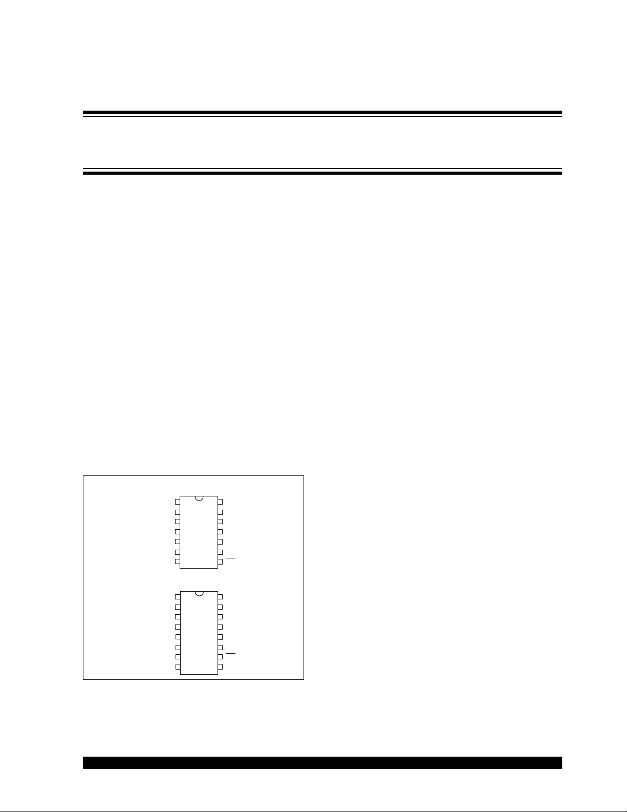
Package Types
PDIP, SOIC, TSSOP
14
CH0
CH1
CH2
CH3
NC
NC
DGND
1
2
3
4
5
6
7
V
13
12
11
10
DD
V
REF
AGND
CLK
D
OUT
D
9
IN
8
CS
/SHDN
MCP3302
General Description
The Microchip Technology Inc. MCP3302/04 13-bit A/D
converters feature full differential inputs and low power
consumption in a small package that is ideal for battery
powered systems and remote data acquisition applications. The MCP3302 is programmable to provide two
differential input pairs or four single ended inputs. The
MCP3304 is programmable and provides four differential input pairs or eight single ended inputs.
Incorporating a successive approximation architecture
with on-board sample and hold circuitry, these 13-bit
A/D converters are specified to have ±1 LSB Differential Nonlinearity (DNL); ±1 LSB Integral Nonlinearity
(INL) for B-grade and ±2 LSB for C-grade devices. The
industry-standard SPI™ serial interface enables 13-bit
A/D converter capability to be added to any PICmicro
microcontroller.
The MCP3302/04 devices feature low current design
that permits operation with typical standby and active
currents of only 50 nA and 300 µA, respectively. The
devices operate over a broad voltage range of 2.7V to
5.5V and are capable of conversion rates of up to
100 ksps. The reference voltage can be varied from
400 mV to 5V, yielding input-referred resolution
between 98 µV and 1.22 mV.
The MCP3302 is available in 14-pin PDIP, 150 mil
SOIC and TSSOP packages. The MCP3304 is available in 16-pin PDIP and 150 mil SOIC packages. The
full differential inputs of these devices enable a wide
variety of signals to be used in applications such as
remote data acquisition, portable instrumentation and
battery operated applications.
®
PDIP, SOIC
16
15
MCP3304
14
13
12
11
10
9
V
DD
V
REF
AGND
CLK
D
OUT
D
IN
CS/SHDN
DGND
1
CH0
CH1
2
CH2
3
4
CH3
CH4
5
CH5
6
CH6
7
CH7
8
2002 Microchip Technology Inc. DS21697B-page 1
Page 2
MCP3302/04
Functional Block Diagram
V
REF
CH0
CH1
CH7
Input
Channel
Mux
*
Sample
& Hold
Circuits
CDAC
Comparator
-
+
AGND
V
DD
13-Bit SAR
DGND
Control Logic
CS/SHDN
CLK
D
IN
Shift
Register
D
OUT
* Channels 5-7 available on MCP3304 Only
DS21697B-page 2 2002 Microchip Technology Inc.
Page 3
MCP3302/04
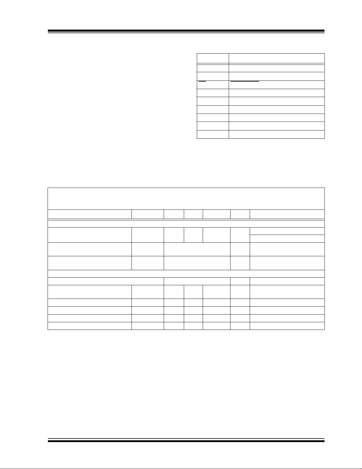
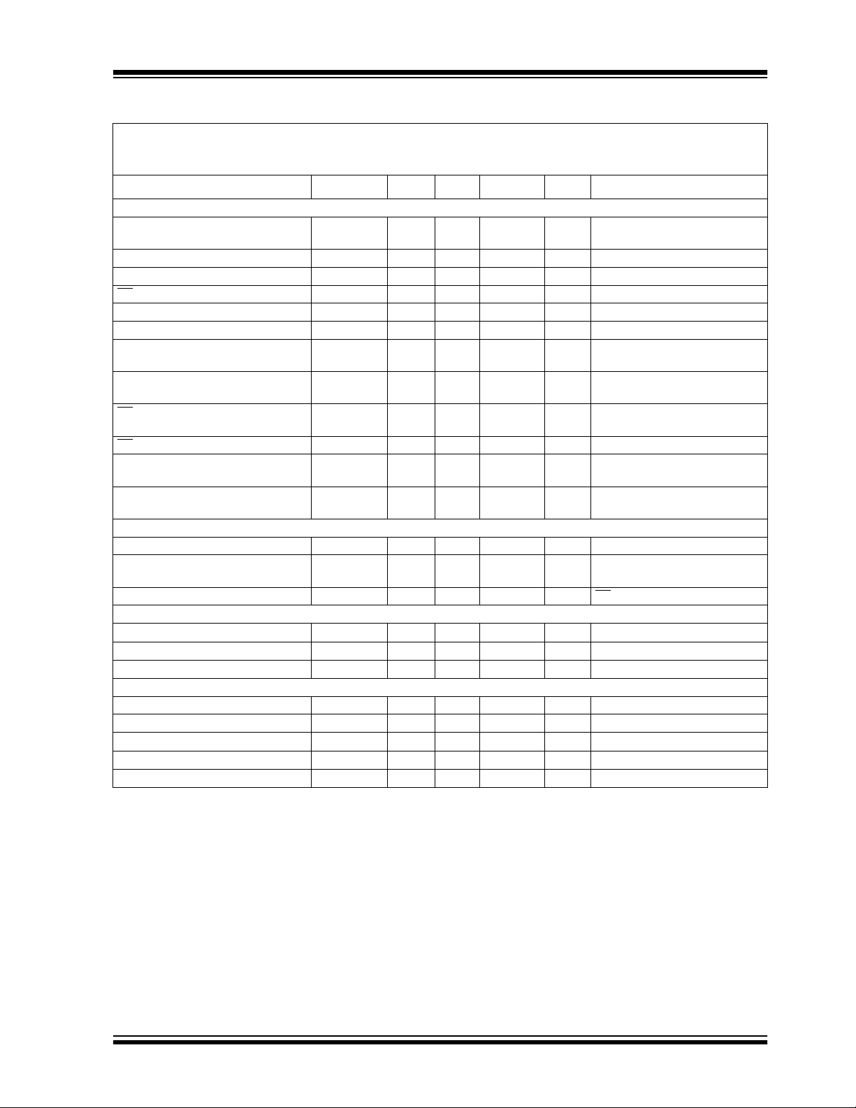
1.0 ELECTRICAL CHARACTERISTICS
Maximum Ratings*
VDD........................................................................ 7.0V
All inputs and outputs w.r.t. V
Storage temperature .......................... -65°C to +150°C
Ambient temp. with power applied ..... -65°C to +125°C
Maximum Junction Temperature ....................... 150°C
ESD protection on all pins (HBM)......................... > 4kV
*Notice: Stresses above those listed under “Maximum ratings” may cause permanent damage to the device. This is a
stress rating only and functional operation of the device at
those or any other conditions above those indicated in the
operational listings of this specification is not implied. Exposure to maximum rating conditions for extended periods may
affect device reliability.
.....-0.3V to VDD +0.3V
SS
PIN FUNCTION TABLE
Name Function
CH0-CH7 Analog Inputs
DGND Digital Ground
/SHDN Chip Select / Shutdown Input
CS
D
IN
D
OUT
CLK Serial Clock
AGND Analog Ground
V
REF
V
DD
Serial Data In
Serial Data Out
Reference Voltage Input
+2.7V to 5.5V Power Supply
ELECTRICAL SPECIFICATIONS
Electrical Characteristics: Unless otherwise noted, all parameters apply at VDD = 5V, VSS = 0V, and V
input configuration (Figure 3-4) with fixed common mode voltage of 2.5V. All parameters apply over temperature with
T
= -40°C to +85°C (Note 7). Conversion speed (F
AMB
Parameter Symbol Min Typ Max Units Conditions
Conversion Rate
Maximum Sampling Frequency F
Conversion Time T
Acquisition Time T
DC Accuracy
Resolution 12 data bits + sign bits
Integral Nonlinearity INL —
Differential Nonlinearity DNL — ±0.5 ±1 LSB Monotonic over temperature
Positive Gain Error -3 -0.75 +2 LSB
Negative Gain Error -3 -0.5 +2 LSB
Offset Error -3 +3 +6 LSB
Note 1: This specification is established by characterization and not 100% tested.
2: See characterization graphs that relate converter performance to V
3: V
= 0.1V to 4.9V @ 1 kHz.
IN
4: V
=5V
DD
5: Maximum clock frequency specification must be met.
6: V
REF
7: TSSOP devices are only specified at 25°C and +85°C.
8: For slow sample rates, see Section 6.2.1 for limitations on clock frequency.
±500 mV @ 1 kHz, see test circuit Figure 3-3.
P-P
= 400 mV, VIN = 0.1V to 4.9V @ 1 kHz
SAMPLE
CONV
ACQ
) is 100 ksps with F
SAMPLE
—— 100kspsNote 8
— — 50 ksps V
13 CLK
1.5 CLK
±0.5
—
±1
±1
±2
REF
CLK
level.
= 21*F
periods
periods
LSB
LSB
SAMPL E
DD
MCP3302/04-B
MCP3302/04-C
= 5V. Full differential
REF
= V
= 2.7V, VCM =1.35V
REF
2002 Microchip Technology Inc. DS21697B-page 3
Page 4
MCP3302/04
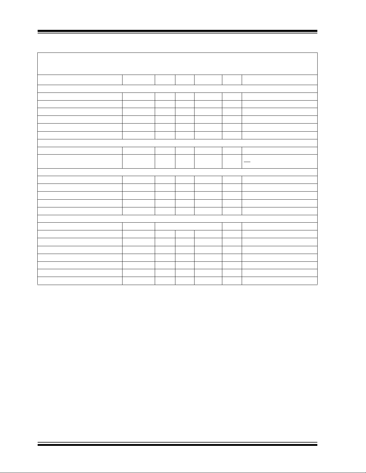
ELECTRICAL SPECIFICATIONS (CONTINUED)
Electrical Characteristics: Unless otherwise noted, all parameters apply at VDD = 5V, VSS = 0V, and V
= 5V. Full differential
REF
input configuration (Figure 3-4) with fixed common mode voltage of 2.5V. All parameters apply over temperature with
T
= -40°C to +85°C (Note 7). Conversion speed (F
AMB
) is 100 ksps with F
SAMPLE
CLK
= 21*F
SAMPL E
Parameter Symbol Min Typ Max Units Conditions
Dynamic Performance
Total Harmonic Distortion THD — -91 — dB Note 3
Signal to Noise and Distortion SINAD — 78 — dB Note 3
Spurious Free Dynamic Range SFDR — 92 — dB Note 3
Common Mode Rejection CMRR — 79 — dB Note 6
Channel to Channel C rosstalk CT — > -110 — dB Note 6
Power Supply Rejection PSR — 74 — dB Note 4
Reference Input
Voltage Range 0.4 — V
Current Drain —
—
100
0.001
VNote 2
DD
150
3
µA
µACS
= VDD = 5V
Analog Inputs
Full Scale Input Span CH0 - CH7 -V
REF
—V
Absolute Input Voltage CH0 - CH7 -0.3 — V
REF
+ 0.3 V
DD
V
Leakage Current — 0.001 ±1 µA
Switch Resistance R
Sample Capacitor C
SAMPLE
S
—1 — kΩ See Figure 6-3
— 25 — pF See Figure 6-3
Digital Input/Output
Data Coding Format Binary Two’s Complement
High Level Input Voltage V
Low Level Input Voltage V
High Level Output Voltage V
Low Level Output Voltage V
Input Leakage Current I
Output Leakage Current I
Pin Capacitance CIN, C
LO
IH
OH
OL
LI
IL
OUT
0.7 V
——0.3 VDDV
4.1 — — V IOH = -1 mA, VDD = 4.5V
—— 0.4 VIOL = 1 mA, VDD = 4.5V
-10 — 10 µAV
-10 — 10 µAV
—— 10 pFT
—— V
DD
= VSS or V
IN
= VSS or V
OUT
= 25°C, F = 1 MHz, Note 1
AMB
DD
DD
Note 1: This specification is established by characterization and not 100% tested.
2: See characterization graphs that relate converter performance to V
3: V
= 0.1V to 4.9V @ 1 kHz.
IN
4: V
=5V
DD
5: Maximum clock frequency specification must be met.
6: V
REF
7: TSSOP devices are only specified at 25°C and +85°C.
±500 mV @ 1 kHz, see test circuit Figure 3-3.
P-P
= 400 mV, VIN = 0.1V to 4.9V @ 1 kHz
REF
level.
8: For slow sample rates, see Section 6.2.1 for limitations on clock frequency.
DS21697B-page 4 2002 Microchip Technology Inc.
Page 5
ELECTRICAL SPECIFICATIONS (CONTINUED)
MCP3302/04
Electrical Characteristics: Unless otherwise noted, all parameters apply at VDD = 5V, VSS = 0V, and V
= 5V. Full differential
REF
input configuration (Figure 3-4) with fixed common mode voltage of 2.5V. All parameters apply over temperature with
T
= -40°C to +85°C (Note 7). Conversion speed (F
AMB
) is 100 ksps with F
SAMPLE
CLK
= 21*F
SAMPL E
Parameter Symbol Min Typ Max Units Conditions
Timing Specifications:
Clock Frequency (Note 8) F
Clock High Time T
Clock Low Time T
Fall To First Rising CLK Edge T
CS
Data In Setup time T
Data In Hold Time T
CLK Fall To Output Data Valid T
CLK Fall To Output Enable T
Rise To Output Disable T
CS
CLK
HI
LO
SUCS
SU
HD
DO
EN
DIS
0.105
0.105——
210 — — ns Note 5
210 — — ns Note 5
100 — — ns
50 — — ns
—— 50 ns
—— 125
—— 125
— — 100 ns See test circuits, Figure 3-1
2.1
1.05
200
200
MHz
MHz
VDD = 5V, F
V
= 2.7V, F
DD
SAMPLE
SAMPLE
= 100 ksps
nsnsVDD = 5V, see Figure 3-1
V
= 2.7V, see Figure 3-1
DD
nsnsVDD = 5V, see Figure 3-1
V
= 2.7V, see Figure 3-1
DD
Note 1
Disable Time T
CS
Rise Time T
D
OUT
CSH
R
475 — — ns
— — 100 ns See test circuits, Figure 3-1
Note 1
Fall Time T
D
OUT
F
— — 100 ns See test circuits, Figure 3-1
Note 1
Power Requirements:
Operating Voltage V
Operating Current I
Standby Current I
DD
DD
DDS
2.7 — 5.5 V
—
—
300
200
450
—
µAV
DD
V
DD
—0.05 1 µACS = V
, V
, V
= 5V, D
REF
= 2.7V, D
REF
= 5.0V
DD
OUT
OUT
Temperature Ranges:
Specified Temperature Range T
Operating Temperature Range T
Storage Temperature Range T
A
A
A
-40 — +85 °C
-40 — +85 °C
-65 — +150 °C
Thermal Package Resistance:
Thermal Resistance, 14L-PDIP θ
Thermal Resistance, 14L-SOIC θ
Thermal Resistance, 14L-TSSOP θ
Thermal Resistance, 16L-PDIP θ
Thermal Resistance, 16L-SOIC θ
JA
JA
JA
JA
JA
—70 — °C/W
—108 — °C/W
—100 — °C/W
—70 — °C/W
—90 — °C/W
Note 1: This specification is established by characterization and not 100% tested.
2: See characterization graphs that relate converter performance to V
3: V
= 0.1V to 4.9V @ 1 kHz.
IN
4: V
=5V
DD
5: Maximum clock frequency specification must be met.
6: V
REF
±500 mV @ 1 kHz, see test circuit Figure 3-3.
P-P
= 400 mV, VIN = 0.1V to 4.9V @ 1 kHz
REF
level.
7: TSSOP devices are only specified at 25°C and +85°C.
8: For slow sample rates, see Section 6.2.1 for limitations on clock frequency.
= 50 ksps
unloaded
unloaded
2002 Microchip Technology Inc. DS21697B-page 5
Page 6
MCP3302/04
.
T
CSH
CS
T
SUCS
CLK
T
T
D
IN
D
OUT
SU
MSB IN
HD
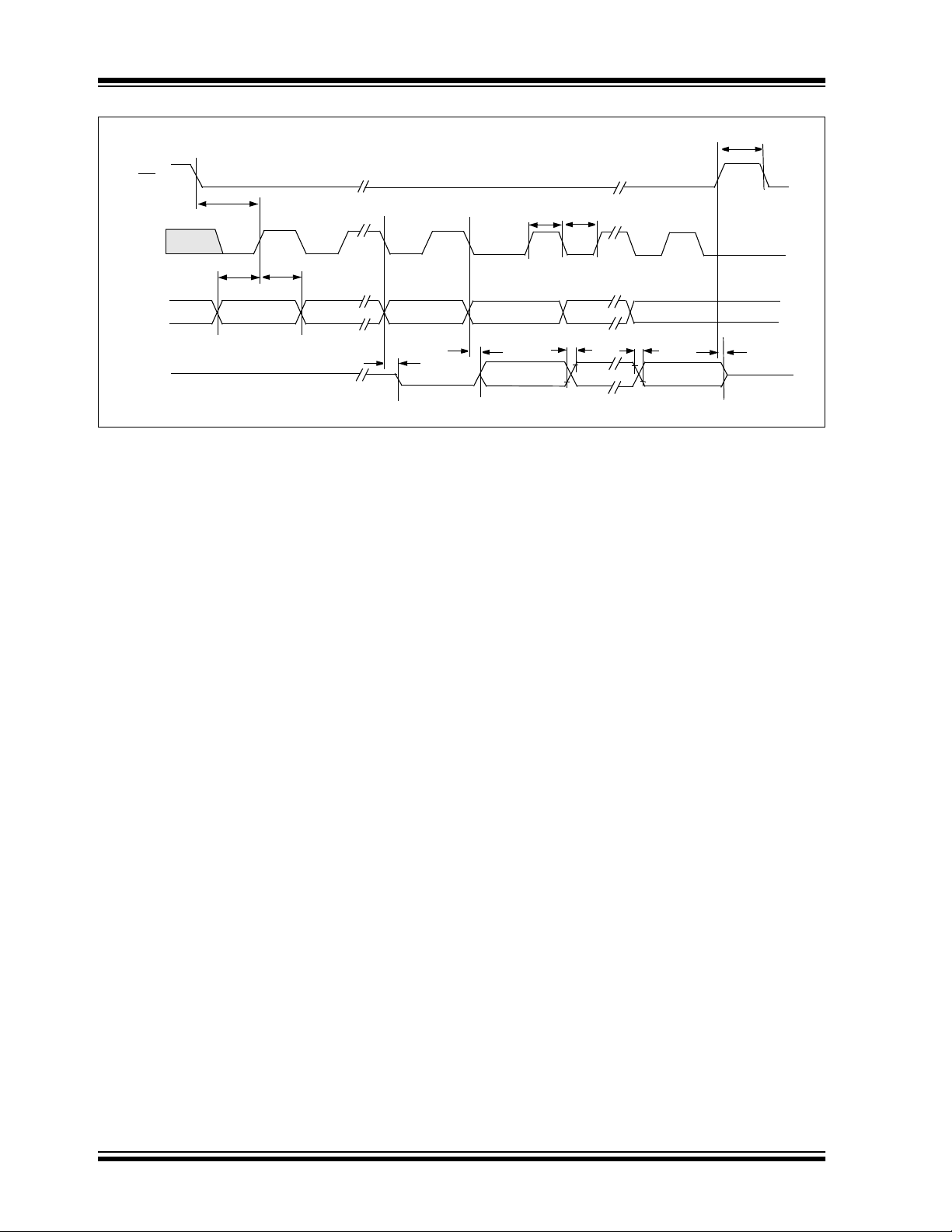
FIGURE 1-1: Timing Parameters
T
T
LO
HI
T
Null Bit
DO
Sign BIT
T
EN
T
R
T
F
T
DIS
LSB
DS21697B-page 6 2002 Microchip Technology Inc.
Page 7
MCP3302/04
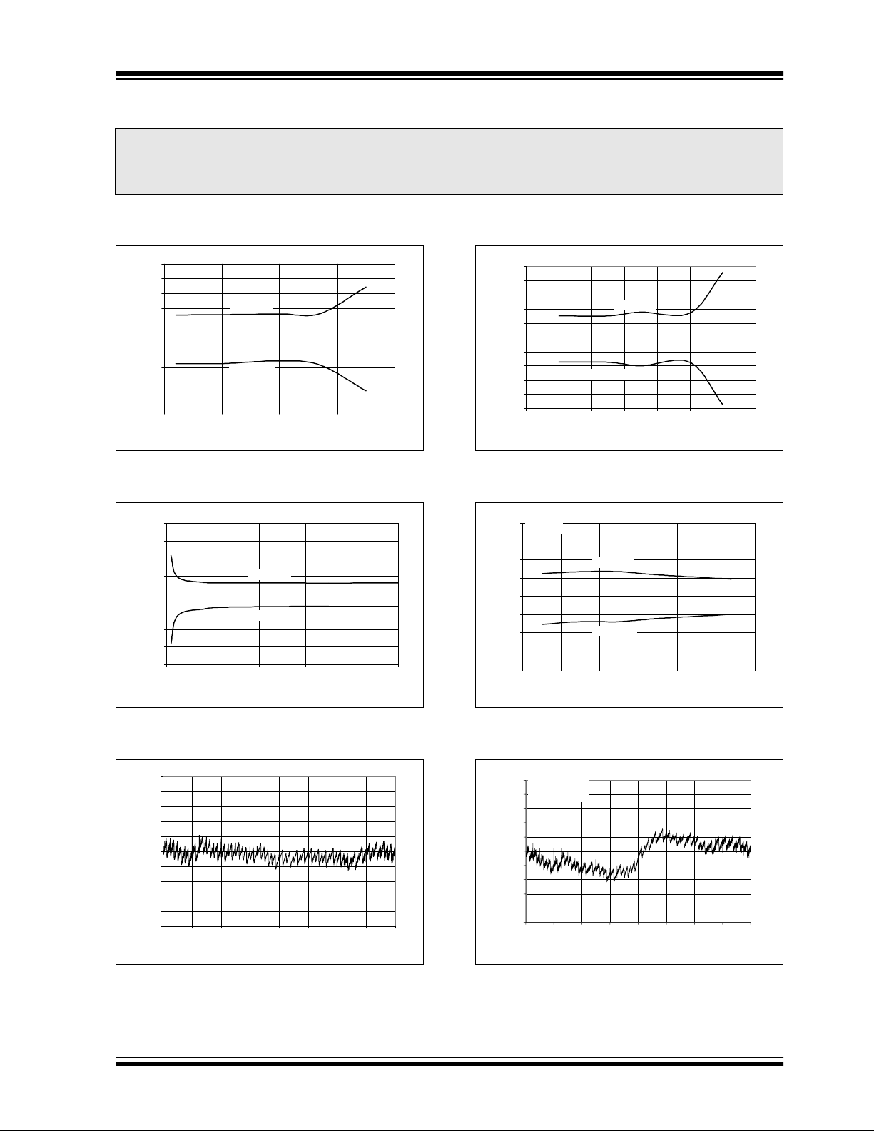
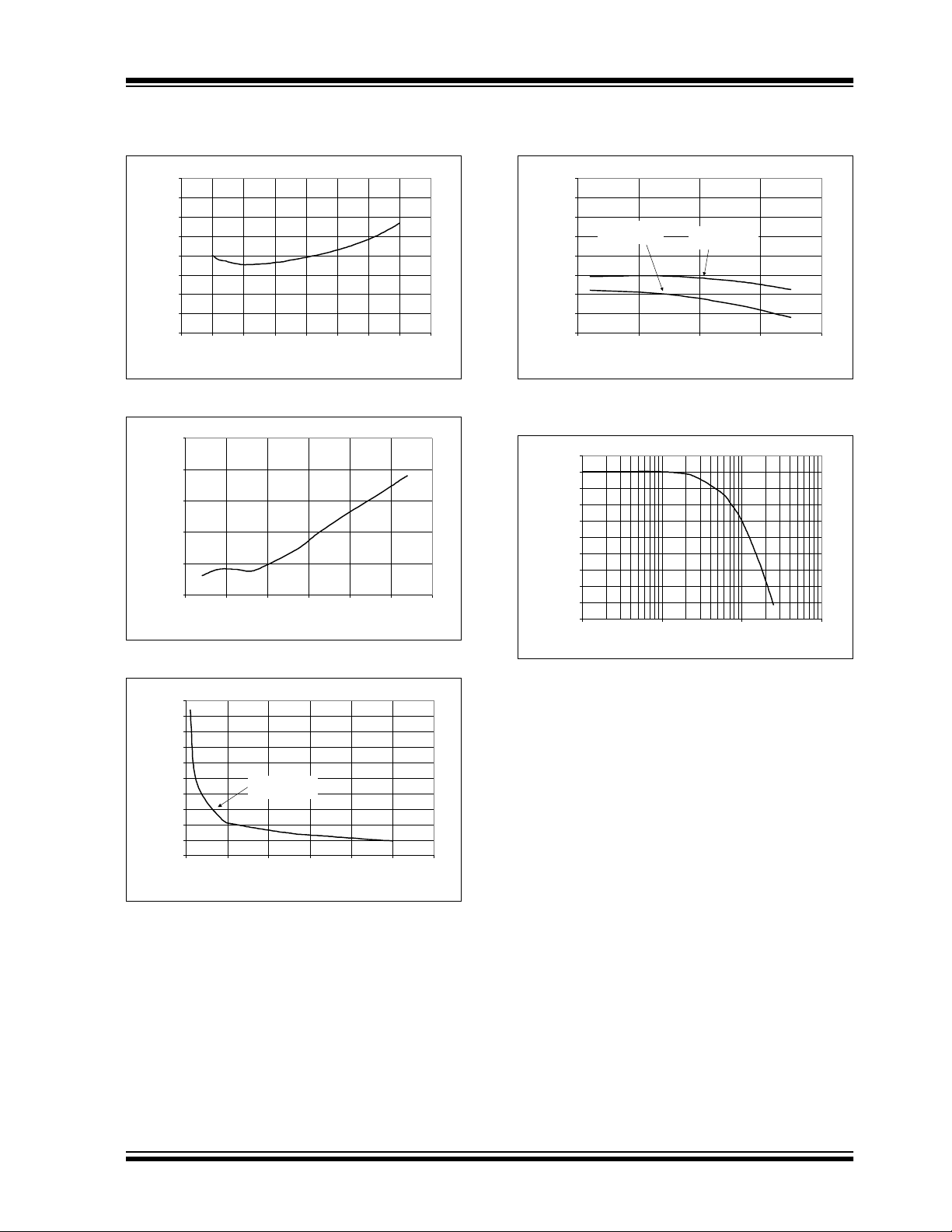
2.0 TYPICAL PERFORMANCE CURVES
Note: The graphs and tables provided following this note are a statistical summary based on a limited number of
samples and are provided for informational purposes only. The performance characteristics listed herein
are not tested or guaranteed. In some graphs or tables, the data presented may be outside the specified
operating range (e.g., outside specified power supply range) and therefore outside the warranted range.
Note: Unless otherwise indicated, V
F
.
1
0.8
0.6
0.4
0.2
0
-0.2
INL (LSB)
-0.4
-0.6
-0.8
-1
0 50 100 150 200
SAMPLE
= 100 ksps, F
Positive INL
Negative INL
Sample Rate (ksps)
CLK
DD
= 21*F
= V
SAMPLE
REF
FIGURE 2-1: Integral Nonlinearity (INL) vs. Sample Rate
2
1.5
1
0.5
0
INL (LSB)
-0.5
-1
-1.5
-2
012345
Positive INL
Negative INL
V
REF
(V)
= 5V, Full differential input configuration, V
, TA = 25°C.
.
1
VDD=V
=2.7V
REF
0.8
0.6
0.4
0.2
0
INL (LSB)
-0.2
-0.4
-0.6
-0.8
-1
0 10203040506070
Positive INL
Negative INL
Sample Rate (ksps)
FIGURE 2-4: Integral Nonlinearity (INL)
vs. Sample Rate (V
.
2
V
= 2.7V
DD
1.5
1
0.5
0
INL(LSB)
-0.5
-1
-1.5
-2
00.511.522.53
= 2.7V)
DD
Positive INL
Negative INL
V
REF
= 0V,
SS
(V)
FIGURE 2-2: Integral Nonlinearity (INL)
vs. V
REF.
1
0.8
0.6
0.4
0.2
0
-0.2
INL (LSB)
-0.4
-0.6
-0.8
-1
-4096 -3072 -2048 -1024 0 1024 2048 3072 4096
Code
FIGURE 2-3: Integral Nonlinearity (INL) vs. Code (Representative Part).
FIGURE 2-5: Integral Nonlinearity (INL)
vs. V
REF (VDD
1
0.8
0.6
0.4
0.2
0
-0.2
INL (LSB)
-0.4
-0.6
-0.8
-1
-4096 -3 072 -204 8 -1 024 0 1024 204 8 3 072 4096
VDD=V
F
SAMPLE
= 2.7V)
=2.7V
REF
= 50 ksps
Code
FIGURE 2-6: Integral Nonlinearity (INL)
vs. Code (Representative Part, V
= 2.7V).
DD
2002 Microchip Technology Inc. DS21697B-page 7
Page 8
MCP3302/04
Note: Unless otherwise indicated, V
F
1
0.8
0.6
0.4
0.2
0
-0.2
INL (LSB)
-0.4
-0.6
-0.8
-1
-50 -25 0 25 50 75 100 125 150
SAMPLE
= 100 ksps, F
Positive INL
Negative INL
Temperature(°C)
CLK
DD
= 21*F
= V
SAMPLE
REF
FIGURE 2-7: Integral Nonlinearity (INL) vs. Temperature.
1
0.8
0.6
0.4
0.2
0
-0.2
DNL (LSB)
-0.4
-0.6
-0.8
-1
0 50 100 150 200
Positive DNL
Negative DNL
Sample Rate (ksps)
= 5V, Full differential input configuration, V
, TA = 25°C.
1
VDD=V
=2.7V
REF
0.8
0.6
0.4
0.2
-0.2
INL (LSB)
-0.4
-0.6
-0.8
= 50 ksps
F
SAMPLE
Positive INL
0
Negative INL
-1
-50-250 255075100125150
Temperature (°C)
FIGURE 2-10: Integral Nonlinearity (INL)
vs. Temperature (V
1
VDD=V
=2.7V
REF
0.8
0.6
0.4
0.2
0
-0.2
DNL (LSB)
-0.4
-0.6
-0.8
-1
0 10203040506070
= 2.7V).
DD
Positive DNL
Negative DNL
Sample Rate (ksps)
SS
= 0V,
FIGURE 2-8: Differential Nonlinearity (DNL) vs. Sample Rate.
2
1.5
1
0.5
0
DNL(LSB)
-0.5
-1
-1.5
-2
0123456
Positive DNL
Negative DNL
V
(V)
REF
FIGURE 2-9: Differential Nonlinearity
(DNL) vs. V
REF
.
FIGURE 2-11: Differential Nonlinearity
(DNL) vs. Sample Rate (V
2
VDD=2.7V
= 50 ksps
F
SAMPLE
1.5
1
0.5
0
DNL (LSB)
-0.5
-1
-1.5
-2
0 0.5 1 1.5 2 2.5 3
Positive DNL
DD
Negative DNL
V
(V)
REF
= 2.7V).
FIGURE 2-12: Differential Nonlinearity
(DNL) vs. V
REF (VDD
= 2.7V).]
DS21697B-page 8 2002 Microchip Technology Inc.
Page 9
MCP3302/04
Note: Unless otherwise indicated, V
F
1
0.8
0.6
0.4
0.2
0
-0.2
DNL (LSB)
-0.4
-0.6
-0.8
-1
-4096 -3072 -2048 -1024 0 1024 2048 3072 4096
SAMPLE
= 100 ksps, F
Code
CLK
DD
= 21*F
= V
SAMPLE
FIGURE 2-13: Differential Nonlinearity (DNL) vs. Code (Representative Part).
1
0.8
0.6
0.4
0.2
0
-0.2
DNL (LSB)
-0.4
-0.6
-0.8
-1
-50 -25 0 25 50 75 100 125 150
Posit ive DNL
Negaitive DNL
Temperature (°C)
= 5V, Full differential input configuration, V
REF
, TA = 25°C.
1
VDD=V
=2.7V
REF
0.8
= 50 ksps
F
SAMPLE
0.6
0.4
0.2
0
-0.2
DNL (LSB)
-0.4
-0.6
-0.8
-1
-4096 -3 072 -204 8 -1024 0 1024 204 8 3072 409 6
FIGURE 2-16: Differential Nonlinearity
(DNL) vs. Code (Representative Part,
V
= 2.7V).
DD
1
VDD=V
=2.7V
REF
0.8
0.6
0.4
0.2
-0.2
DNL (LSB)
-0.4
-0.6
-0.8
= 50 ksps
F
SAMPLE
0
-1
-50 -25 0 25 50 75 100 125 150
SS
Code
Positive DNL
Negative DNL
Temperature (°C)
= 0V,
FIGURE 2-14: Differential Nonlinearity (DNL) vs. Temperature.
4
3
2
1
0
-1
Positive Gain Error (LSB)
-2
-3
0123456
VDD=5V
F
SAMPLE
= 100 ksps
V
REF
(V)
FIGURE 2-15: Positive Gain Error vs.
.
V
REF
FIGURE 2-17: Differential Nonlinearity
(DNL) vs. Temperature (V
20
18
16
14
12
10
8
6
Offset Error (LSB)
4
V
= 2.7V
DD
2
F
SAMPLE
0
0123456
= 50 ksps
V
F
DD
SAMPLE
= 5V
= 100 ksp s
FIGURE 2-18: Offset Error vs. V
DD
V
REF
= 2.7V).
(V)
REF
.
2002 Microchip Technology Inc. DS21697B-page 9
Page 10
MCP3302/04
Note: Unless otherwise indicated, V
F
0
-0.2
-0.4
-0.6
-0.8
-1
-1.2
-1.4
VDD=V
Positive Gain Error (LSB)
F
-1.6
-1.8
-50 0 50 100 150
SAMPLE
=2.7V
REF
= 50 ksps
SAMPLE
= 100 ksps, F
Temperature (°C)
CLK
VDD=V
F
SAMPLE
DD
= 21*F
=5V
REF
= 100 ksps
= V
SAMPLE
FIGURE 2-19: Positive Gain Error vs. Temperature.
100
90
80
70
60
50
SNR (db)
40
30
20
10
0
110100
Input Frequency (kHz)
VDD=V
F
SAMPLE
VDD=V
F
SAMPLE
=5V
REF
= 100 ksp s
=2.7V
REF
= 50 ksps
= 5V, Full differential input configuration, V
REF
, TA = 25°C.
3.5
3
2.5
2
1.5
1
Offset Error (LSB)
0.5
0
-50 0 50 100 150
FIGURE 2-22: Offset Error vs. Temperature.
90
80
70
60
VDD=V
=2.7V
REF
= 50 ksps
F
SAMPLE
50
40
SINAD (dB)
30
20
10
0
110100
= 0V,
SS
VDD=V
REF
F
= 100 ksp s
SAMPLE
VDD=V
=2.7V
REF
F
= 50 ksps
SAMPLE
Temperature (°C)
Input Frequency (kHz)
=5V
VDD=V
F
SAMPLE
=5V
REF
= 100 ksps
FIGURE 2-20: Signal to Noise Ratio (SNR) vs. Input Frequency.
0
-10
-20
-30
-40
-50
THD (dB)
-60
-70
-80
-90
-100
VDD=V
=2.7V
REF
F
= 50 ksps
SAMPLE
110100
Input Frequency (kHz)
VDD=V
F
SAMPLE
=5V
REF
= 100 ksp s
FIGURE 2-21: Total Harmonic Distortion (THD) vs. Input Frequency.
FIGURE 2-23: Signal to Noise and Distortion (SINAD) vs. Input Frequency.
80
70
60
50
40
VDD=V
F
SAMPLE
=2.7V
REF
= 50 ksps
30
SINAD (dB)
20
10
0
-40 -35 -30 -2 5 -20 -15 -10 -5 0
VDD=V
F
SAMPLE
=5V
REF
= 100 ksps
Input Signal Level (dB)
FIGURE 2-24: Signal to Noise and Distortion (SINAD) vs. Input Signal Level.
DS21697B-page 10 2002 Microchip Technology Inc.
Page 11
MCP3302/04
= 21*F
= 100 ksps
SAMPLE
DD
= V
SAMPLE
REF
Note: Unless otherwise indicated, V
F
13
12
11
10
ENOB (rms)
9
8
7
012345
SAMPLE
= 100 ksps, F
VDD=2.7V
= 50 ksps
F
SAMPLE
V
(V)
REF
CLK
VDD=5V
F
FIGURE 2-25: Effective Number of Bits
(ENOB) vs. V
100
90
80
70
60
50
40
SFDR (dB)
30
20
10
0
110100
REF
VDD=V
F
SAMPLE
.
=2.7V
REF
= 50 ksps
Input Frequency (kHz)
VDD=V
F
SAMPLE
=5V
REF
= 100 ksps
= 5V, Full differential input configuration, V
, TA = 25°C.
13
12.8
12.6
12.4
12.2
12
ENOB (rms)
11.8
11.6
11.4
11.2
110100
VDD=V
=2.7V
REF
= 50 ksps
F
SAMPLE
Input Frequency (kHz)
FIGURE 2-28: Effective Number of Bits (ENOB) vs. Input Frequency.
-30
-35
-40
-45
-50
-55
PSR(dB)
-60
-65
-70
-75
-80
1 10 100 1000 10000
Ripple Frequency (kHz)
SS
= 0V,
VDD=V
=5V
REF
= 100 ksps
F
SAMPLE
0.1 µF Bypass
Capacitor
FIGURE 2-26: Spurious Free Dynamic Range (SFDR) vs. Input Frequency.
0
-10
-20
-30
-40
-50
-60
-70
-80
-90
-100
Amplitude (dB)
-110
-120
-130
-140
-150
0 10000 20000 30000 40000 50000
Frequency (Hz)
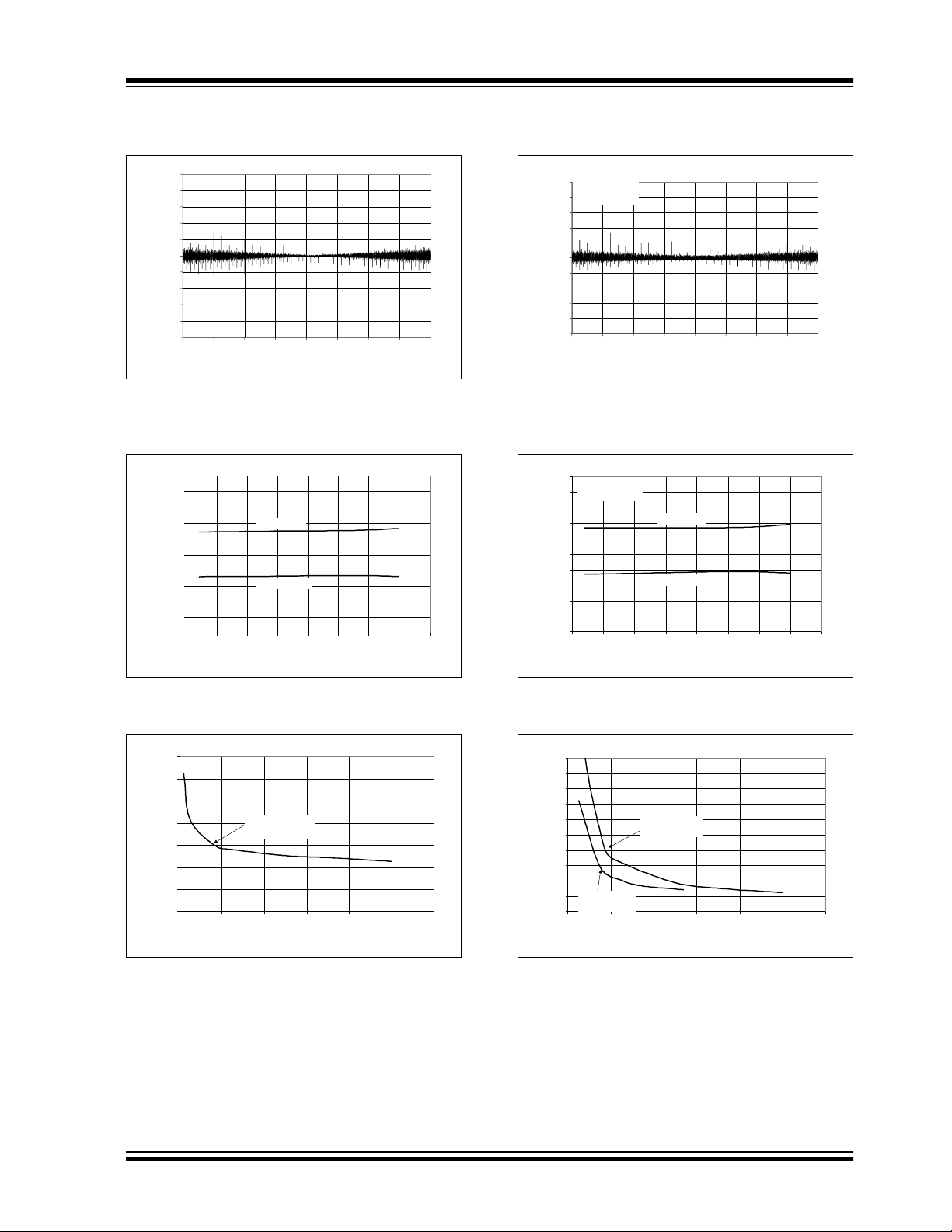
FIGURE 2-27: Frequency Spectrum of
10 kHz Input (Representative Part).
FIGURE 2-29: Power Supply Rejection (PSR) vs. Ripple Frequency.
0
-10
-20
-30
-40
-50
-60
-70
-80
-90
-100
Amplitude (dB)
-110
-120
-130
-140
-150
0 5000 10000 15000 20000 25000
Frequency (Hz)
FIGURE 2-30: Frequency Spectrum of
1 kHz Input (Representative Part, V
DD
= 2.7V).
2002 Microchip Technology Inc. DS21697B-page 11
Page 12
MCP3302/04
Note: Unless otherwise indicated, V
F
450
400
350
300
250
(µA)
200
DD
I
150
100
50
0
22.533.544.555.56
FIGURE 2-31: I
600
500
400
300
(µA)
DD
I
200
100
0
0 50 1 00 150 200
SAMPLE
= 100 ksps, F
VDD (V)
vs. VDD.
DD
VDD=V
=5V
REF
VDD=V
=2.7V
REF
Sample Rate (ksps)
CLK
DD
= 21*F
= V
SAMPLE
= 5V, Full differential input configuration, V
REF
, TA = 25°C.
120
100
80
(µA)
60
REF
I
40
20
0
22.533.544.555.56
FIGURE 2-34: I
120
VDD=V
REF
0 5 0 100 150 200
(µA)
REF
I
100
80
60
40
20
0
SS
VDD (V)
vs. VDD.
REF
=5V
VDD=V
=2.7V
REF
Sample Rate (ksps)
= 0V,
FIGURE 2-32: I
400
350
300
250
200
(µA)
DD
I
150
100
50
0
-50 0 50 100 150
FIGURE 2-33: I
vs. Sample Rate.
DD
VDD=V
=5V
REF
= 100 ksps
F
SAMPLE
VDD=V
=2.7V
REF
F
= 50 ksps
SAMPLE
Temperature (°C)
vs. Temperature.
DD
FIGURE 2-35: I
100
90
80
70
60
(µA)
50
REF
I
40
30
20
10
0
-50 0 50 100 150
FIGURE 2-36: I
vs. Sample Rate.
REF
VDD=V
REF
F
SAMPLE
VDD=V
F
SAMPLE
Temperature (°C)
vs. Temperature.
REF
=5V
= 100 ksps
=2.7V
REF
= 50 ksps
DS21697B-page 12 2002 Microchip Technology Inc.
Page 13
MCP3302/04
Note: Unless otherwise indicated, V
F
80
70
60
50
(pA)
40
DDS
I
30
20
10
0
22.533.544.555.56
FIGURE 2-37: I
100
10
1
(nA)
DDS
0.1
I
0.01
0.001
-50 -25 0 25 50 75 100
FIGURE 2-38: I
4
3.5
3
2.5
2
1.5
1
0.5
0
Negative Gain Error (LSB)
-0.5
-1
0123456
SAMPLE
= 100 ksps, F
V
(V)
DD
vs. VDD.
DDS
Temperature (°C)
vs. Temperature.
DDS
VDD=5V
= 100 ksps
F
SAMPLE
V
(V)
REF
CLK
DD
= 21*F
= V
SAMPLE
= 5V, Full differential input configuration, V
REF
, TA = 25°C.
2
1.5
1
VDD=V
=2.7V
F
SAMPLE
REF
= 50 ksps
0.5
0
-0.5
-1
Negative Gain Error (LSB)
-1.5
-2
-50 0 50 100 150
FIGURE 2-40: Negative Gain Error vs. Temperature.
80
79
78
77
76
75
74
73
72
71
Common Mode Rejection Ration(dB)
70
1 10 100 1000
FIGURE 2-41: Common Mode Rejection vs. Frequency.
= 0V,
SS
VDD=V
=5V
REF
= 100 ksps
F
SAMPLE
Temperature (°C)
Input Frequency (kHz)
FIGURE 2-39: Negative Gain Error vs. Reference Voltage.
2002 Microchip Technology Inc. DS21697B-page 13
Page 14

MCP3302/04
3.0 TEST CIRCUITS
1.4V
3k
Ω
CL = 100 pF
MCP330X
D
OUT
Tes t Poi nt
2.63V
1kΩ
20 kΩ
5VP-P
+
-
1kΩ
1/2
1kΩ
MCP602
5V ±500 mV
To VDD on DUT
P-P
FIGURE 3-1: Load Circuit for T
Test Po i n t
V
DD
3k
D
MCP330X
OUT
Ω
100 pF
V
Voltage Waveforms for T
CS
D
OUT
Waveform 1*
D
OUT
Waveform 2†
*Waveform 1 is for an output with internal conditions such that the output is high, unless disabled by the output control.
†Waveform 2 is for an output with internal conditions such that the output is low, unless disabled by the output control.
VDD/2
SS
T
DIS
T
Waveform 2
DIS
TEN Waveform
Waveform 1
T
DIS
V
IH
, TF, TDO.
R
DIS
90%
10%
FIGURE 3-3: Power Supply Sensitivity Test Circuit (PSRR).
REFVDD
V
SS
VDD = 5V
0.1 µF
5V
5V
VCM = 2.5V
P-P
P-P
IN(+)
IN(-)
V
= 5V
REF
1µF
0.1 µF
MCP330X
V
FIGURE 3-4: Full Differential Test Configuration Example.
5V
P-P
IN(+)
IN(-)
V
REF
MCP330X
= 2.5V
1µF
0.1µF
V
REFVDD
V
SS
VDD = 5V
0.1µF
V
= 2.5V
FIGURE 3-2: Load circuit for
T
.
EN
T
DIS
and
CM
FIGURE 3-5: Pseudo Differential Test Configuration Example.
DS21697B-page 14 2002 Microchip Technology Inc.
Page 15

MCP3302/04
4.0 PIN DESCRIPTIONS
The descriptions of the pins are listed in Table 4-1.
TABLE 4-1: PIN FUNCTION TABLE
Name Function
CH0-CH7 Analog Inputs
DGND Digital Ground
CS
/SHDN Chip Select / Shutdown Input
D
IN
D
OUT
CLK Serial Clock
AGND Analog Ground
V
REF
V
DD
4.1 CH0-CH7
Analog input channels. These pins have an absolute
voltage range of V
differential input range is defined as the absolute value
of (IN+) - (IN-). This difference can not exceed the
value of V
occur.
4.2 DGND
Serial Data In
Serial Data Out
Reference Voltage Input
+2.7V to 5.5V Power Supply
- 0.3V to V
SS
- 1 LSB or digital code saturation will
REF
+ 0.3V. The full scale
DD
4.6 Serial Clock (CLK)
The SPI clock pin is used to initiate a conversion and to
clock out each bit of the conversion as it takes place.
See Section 6.2 for constraints on clock speed. See
Figure 7-2 for serial communication protocol.
4.7 AGND
Ground connection to internal analog circuitry. To
ensure accuracy, this pin must be connected to the
same ground as DGND. If an analog ground plane is
available, it is recommended that this device be tied to
the analog ground plane in the circuit. See Section 6.6
for more information regarding circuit layout.
4.8 Voltage Reference (V
This input pin provides the reference voltage for the
device, which determines the maximum range of the
analog input signal and the LSB size.
The LSB size is determined according to the equation
shown below. As the reference input is reduced, the
LSB size is reduced accordingly.
EQUATION
LSB Size =
2 x V
8192
REF
REF
)
Ground connection to internal digital circuitry. To
ensure accuracy this pin must be connected to the
same ground as AGND. If an analog ground plane is
available, it is recommended that this device be tied to
the analog ground plane in the circuit. See Section 6.6
for more information regarding circuit layout.
4.3 Chip Select/Shutdown (CS/SHDN)
The CS/SHDN pin is used to initiate communication
with the device when pulled low. This pin will end a conversion and put the device in low power standby when
pulled high. The CS
between conversions and cannot be tied low for multiple conversions. See Figure 7-2 for serial communication protocol.
/SHDN pin must be pulled high
4.4 Serial Data Input (DIN)
The SPI port serial data input pin is used to clock in
input channel configuration data. Data is latched on the
rising edge of the clock. See Figure 7-2 for serial communication protocol.
4.5 Serial Data Output (D
The SPI serial data output pin is used to shift out the
results of the A/D conversion. Data will always change
on the falling edge of each clock as the conversion
takes place. See Figure 7-2 for serial communication
protocol.
OUT
)
When using an external voltage reference device, the
system designer should always refer to the manufacturer’s recommendations for circuit layout. Any instability in the operation of the reference device will have a
direct effect on the accuracy of the ADC conversion
results.
4.9 V
The voltage on this pin can range from 2.7 to 5.5V. To
ensure accuracy, a 0.1 µF ceramic bypass capacitor
should be placed as close as possible to the pin. See
Section 6.6 for more information regarding circuit layout.
DD
2002 Microchip Technology Inc. DS21697B-page 15
Page 16

MCP3302/04
5.0 DEFINITION OF TERMS
Bipolar Operation - This applies to either a differential
or single ended input configuration, where both positive
and negative codes are output from the A/D converter.
Full bipolar range includes all 8192 codes. For bipolar
operation on a single ended input signal, the A/D converter must be configured to operate in pseudo differential mode.
Unipolar Operation - This applies to either a single
ended or differential input signal where only one side of
the device transfer is being used. This could be either
the positive or negative side, depending on which input
(IN+ or IN-) is being used for the DC bias. Full unipolar
operation is equivalent to a 12-bit converter.
Full Differential Operation - Applying a full differential
signal to both the IN(+) and IN(-) inputs is referred to as
full differential operation. This configuration is
described in Figure 3-4.
Pseudo-Differential Operation - Applying a single
ended signal to only one of the input channels with a
bipolar output is referred to as pseudo differential oper-
ation. To obtain a bipolar output from a single ended
input signal the inverting input of the A/D converter
must be biased above V
in Figure 3-5.
Integral Nonlinearity - The maximum deviation from a
straight line passing through the endpoints of the bipolar transfer function is defined as the maximum integral
nonlinearity error. The endpoints of the transfer function are a point 1/2 LSB above the first code transition
(0x1000) and 1/2 LSB below the last code transition
(0x0FFF).
Differential Nonlinearity - The difference between two
measured adjacent code transitions and the 1 LSB
ideal is defined as differential nonlinearity.
Positive Gain Error - This is the deviation between the
last positive code transition (0x0FFF) and the ideal voltage level of V
-1/2 LSB, after the bipolar offset error
REF
has been adjusted out.
Negative Gain Error - This is the deviation between
the last negative code transition (0X1000) and the ideal
voltage level of -V
REF
error has been adjusted out.
Offset Error - This is the deviation between the first
positive code transition (0x0001) and the ideal 1/2 LSB
voltage level.
Acquisition Time - The acquisition time is defined as
the time during which the internal sample capacitor is
charging. This occurs for 1.5 clock cycles of the external CLK as defined in Figure 7-2.
Conversion Time - The conversion time occurs imme-
diately after the acquisition time. During this time, suc-
cessive approximation of the input signal occurs as the
13-bit result is being calculated by the internal circuitry.
This occurs for 13 clock cycles of the external CLK as
defined in Figure 7-2.
. This operation is described
SS
-1/2 LSB, after the bipolar offset
Signal to Noise Ratio - Signal to Noise Ratio (SNR) is
defined as the ratio of the signal to noise measured at
the output of the converter. The signal is defined as the
rms amplitude of the fundamental frequency of the
input signal. The noise value is dependant on the
device noise as well as the quantization error of the
converter and is directly affected by the number of bits
in the converter. The theoretical signal to noise ratio
limit based on quantization error only for an N-bit converter is defined as:
EQUATION
SNR 6.02N 1.76+()dB=
For a 13-bit converter, the theoretical SNR limit is
80.02 dB.
Total Harmonic Distortion - Total Harmonic Distortion
(THD) is the ratio of the rms sum of the harmonics to
the fundamental, measured at the output of the converter. For the MCP3302/04, it is defined using the first
9 harmonics, as is shown in the following equation:
EQUATION
2
2
THD(-dB) 20 log–
=
V
+++ ++
2
------------------------- ------------ ------------- ------------- -----------
2
V
V
3
4
2
V
1
..... V
2
2
V
8
9
Here V1 is the rms amplitude of the fundamental and V
through V9 are the rms amplitudes of the second
through ninth harmonics.
Signal to Noise plus Distortion (SINAD) - Numeri-
cally defined, SINAD is the calculated combination of
SNR and THD. This number represents the dynamic
performance of the converter, including any harmonic
distortion.
EQUATION
SINAD(dB) 20 log 10
EffectIve Number of Bits - Effective Number of Bits
(ENOB) states the relative performance of the ADC in
terms of its resolution. This term is directly related to
SINAD by the following equation:
SNR 10⁄()10THD 10⁄()–
+=
EQUATION
ENOB N()
For SINAD performance of 78 dB, the effective number
of bits is 12.66.
Spurious Free Dynamic Range - Spurious Free
Dynamic Range (SFDR) is the ratio of the rms value of
the fundamental to the next largest component in
ADC’s output spectrum. This is, typically, the first harmonic, but could also be a noise peak.
SINAD 1.76–
------------------------ ----------=
6.02
2
DS21697B-page 16 2002 Microchip Technology Inc.
Page 17

MCP3302/04
6.0 APPLICATIONS INFORMATION
6.1 Conversion Description
The MCP3302/04 A/D converters employ a conventional SAR architecture. With this architecture, the
potential between the IN+ and IN- inputs are simultaneously sampled and stored with the internal sample
circuits for 1.5 clock cycles. Following this sampling
time, the input hold switches of the converter open and
the device uses the collected charge to produce a
serial 13-bit binary two’s complement output code. This
conversion process is driven by the external clock and
must include 13 clock cycles, one for each bit. During
this process, the most significant bit (MSB) is output
first. This bit is the sign bit and indicates if the IN+ or INinput is at a higher potential.
+
-
Comp
CDAC
13-Bit SAR
Shift
Register
D
OUT
IN+
IN-
Hold
Hold
C
C
SAMP
SAMP
6.2 Driving the Analog Input
The analog input of the MCP3302/04 is easily driven,
either differentially or single ended. Any signal that is
common to the two input channels will be rejected by
the common mode rejection of the device. During the
charging time of the sample capacitor, a small charging
current will be required. For low source impedances,
this input can be driven directly. For larger source
impedances, a larger acquisition time will be required
due to the RC time constant that includes the source
impedance. For the A/D Converter to meet specification, the charge holding capacitor (C
given enough time to acquire a 13-bit accurate voltage
level during the 1.5 clock cycle acquisition period.
An analog input model is shown in Figure 6-3. This
model is accurate for an analog input, regardless if it is
configured as a single ended input, or the IN+ and INinput in differential mode. In this diagram, it is shown
that the source impedance (R
sampling switch (R
) impedance, directly affecting the
SS
) adds to the internal
S
time that is required to charge the capacitor (C
Consequently, a larger source impedance with no additional acquisition time increases the offset, gain and
integral linearity errors of the conversion. To overcome
this, a slower clock speed can be used to allow for the
longer charging time. Figure 6-2 shows the maximum
clock speed associated with source impedances.
2.5
SAMPLE
) must be
SAMPLE
).
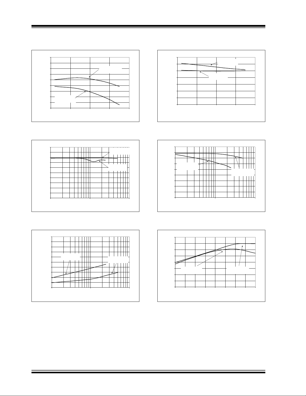
FIGURE 6-1: Simplified Block Diagram.
2.0
1.5
1.0
0.5
Maximum Clock Frequency (MHz)
0.0
100 1000 10000 10000 0
Source Resistance (ohms)
FIGURE 6-2: Maximum Clock Frequency
vs. Source Resistance (R
) to maintain ±1 LSB
S
INL.
2002 Microchip Technology Inc. DS21697B-page 17
Page 18

MCP3302/04
CHx
R
SS
VA
Legend
I
LEAKAGE
C
SAMPLE
R
CHx
C
PIN
signal source
VA
=
source impedance
=
SS
input channel pad
=
input pin capacitance
=
threshold voltage
=
V
T
leakage current at the pin
=
due to various junctions
sampling switch
SS
=
sampling switch resist or
=
R
S
sample/hold capacitance
=
C
7pF
PIN
V
DD
V
T
= 0.6V
V
T
= 0.6V
I
LEAKAGE
±1 nA
Sampling
Switch
R
SS
= 1 kΩ
S
C
SAMPLE
= DAC capacitance
= 25 pF
V
SS
FIGURE 6-3: Analog Input Model.
6.2.1 MAINTAINING MINIMUM CLOCK
SPEED
When the MCP3302/04 initiates, charge is stored on
the sample capacitor. When the sample period is complete, the device converts one bit for each clock that is
received. It is important for the user to note that a slow
clock rate will allow charge to bleed off the sample cap
while the conversion is taking place. For the MCP330X
devices, the recommended minimum clock speed during the conversion cycle (T
) is 105 kHz. Failure to
CONV
meet this criteria may induce linearity errors into the
conversion outside the rated specifications. It should
be noted that during the entire conversion cycle, the
A/D converter does not have requirements for clock
speed or duty cycle, as long as all timing specifications
are met.
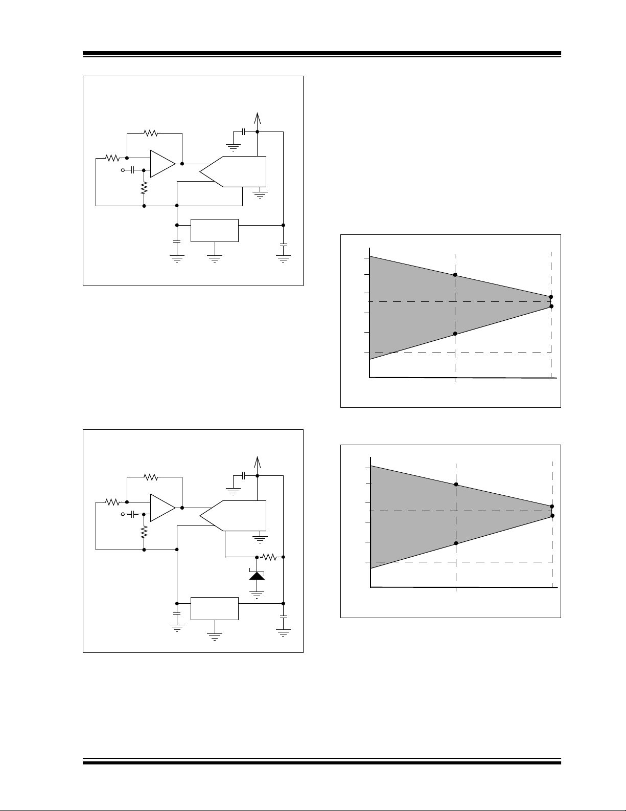
6.3 Biasing Solutions
For pseudo-differential bipolar operation, the biasing
circuit (shown in Figure 6-4) shows a single ended
input AC coupled to the converter. This configuration
will give a digital output range of -4096 to +4095. With
the 2.5V reference, the LSB size equal to 610 µV.
Although the ADC is not production tested with a 2.5V
reference as shown, linearity will not change more than
0.1 LSB. See Figure 2-2 and Figure 2-9 for DNL and
INL errors versus V
between the high pass corner and the acquisition time.
The value of C will need to be quite large in order to
at VDD = 5V. A trade-off exists
REF
bring down the high pass corner. The value of R will
need to be 1 kΩ, or less, since higher input impedances
require additional acquisition time. Using the RC values
in Figure 6-4, we have a 100 Hz corner frequency. See
Figure 2-12 for relation between input impedance and
acquisition time.
VDD = 5V
0.1 µF
C
10 µF
V
IN
1kΩ
1µF
R
IN+
IN-
V
OUT
MCP1525
MCP330X
V
REF
V
IN
0.1 µF
FIGURE 6-4: Pseudo-differential biasing circuit for bipolar operation.
Using an external operation amplifier on the input
allows for gain and also buffers the input signal from the
input to the ADC allowing for a higher source impedance. This circuit is shown in Figure 6-5.
DS21697B-page 18 2002 Microchip Technology Inc.
Page 19
MCP3302/04
6.4 Common Mode Input Range
VDD = 5V
0.1 µF
MCP330X
V
REF
V
IN
0.1 µF
1kΩ
V
IN
1 µF
10 kΩ
MCP6021
-
+
1MΩ
1 µF
IN+
IN-
V
OUT
MCP1525
FIGURE 6-5: Adding an amplifier allows
for gain and also buffers the input from any high
impedance sources.
This circuit shows that some headroom will be lost due
to the amplifier output not being able to swing all the
way to the rail. An example would be for an output
swing of 0V to 5V. This limitation can be overcome by
supplying a V
mode voltage. Using a 2.048V reference for the A/D
converter while biasing the input signal at 2.5V solves
the problem. This circuit is shown in Figure 6-5.
1kΩ
V
IN
that is slightly less than the common
REF
1µF
10 kΩ
MCP606
-
+
1MΩ
1µF
IN+
IN-
V
OUT
MCP1525
0.1 µF
MCP330X
V
REF
2.048V
V
IN
VDD = 5V
10 kΩ
0.1 µF
The common mode input range has no restriction and is
equal to the absolute input voltage range: V
V
+ 0.3V. However, for a given V
DD
REF
-0.3V to
SS
, the common
mode voltage has a limited swing, if the entire range of
the A/D converter is to be used. Figure 6-7 and
Figure 6-8 show the relationship between V
common mode voltage swing. A smaller V
wider flexibility in a common mode voltage. V
REF
allows for
REF
REF
and the
levels,
down to 400 mv, exhibit less than 0.1 LSB change in
DNL and INL. For characterization graphs that show
this performance relationship, see Figure 2-9 and
Figure 2-12.
V
= 5V
DD
5
4
3
2
1
0
Common Mode Range (V)
-1
0.25
1.0
4.05V
2.8V
2.3V
0.95V
2.5
V
(V)
REF
4.0
5.0
FIGURE 6-7: Common Mode Input Range
of Full Differential Input Signal versus V
5
V
REF
4.05V
0.95V
1.25
(V)
4
3
2
1
0
Common Mode Range (V)
-1
0.25
0.5
2.0
REF
V
DD
.
= 5V
2.8V
2.3V
2.5
FIGURE 6-8: Common Mode Input Range
versus V
for Pseudo Differential Input.
REF
FIGURE 6-6: Circuit solution to overcome amplifier output swing limitation.
2002 Microchip Technology Inc. DS21697B-page 19
Page 20

MCP3302/04
6.5 Buffering/Filtering the Analog Inputs
Inaccurate conversion results may occur if the signal
source for the A/D converter is not a low impedance
source. Buffering the input will overcome the impedance issue. It is also recommended that an analog filter
be used to eliminate any signals that may be aliased
back into the conversion results. This is illustrated in
Figure 6-9, where an op amp is used to drive the analog input of the MCP3302/04. This amplifier provides a
low impedance source for the converter input and a low
pass filter, which eliminates unwanted high frequency
noise. Values shown are for a 10 Hz Butterworth Low
Pass filter.
Low pass (anti-aliasing) filters can be designed using
Microchip’s interactive FilterLab
will calculate capacitor and resistor values, as well as
determine the number of poles that are required for the
application. For more information on filtering signals,
see Application Note 699 “Anti-Aliasing Analog Filters
for Data Acquisition Systems”.
4.096V
Reference
7.86 kΩ
V
IN
0.1 µF
2.2 µF
14.6 kΩ
1µF
MCP1541
MCP601
+
-
®
software. FilterLab
1µF
C
L
V
REF
IN+
MCP330X
IN-
V
DD
10 µF
0.1 µF
6.6 Layout Considerations
When laying out a printed circuit board for use with
analog components, care should be taken to reduce
noise wherever possible. A bypass capacitor from V
to ground should always be used with this device and
should be placed as close as possible to the device pin.
A bypass capacitor value of 0.1 µF is recommended.
Digital and analog traces on the board should be separated as much as possible, with no traces running
underneath the device or the bypass capacitor. Extra
precautions should be taken to keep traces with high
frequency signals (such as clock lines) as far as possible from analog traces.
Use of an analog ground plane is recommended in
order to keep the ground potential the same for all
devices on the board. Providing V
connections to
DD
devices in a “star” configuration can also reduce noise
by eliminating current return paths and associated
errors (see Figure 6-10). For more information on layout tips when using the MCP3302/04, or other ADC
devices, refer to Application Note 688, “Layout Tips for
12-Bit A/D Converter Applications”.
V
DD
Connection
Device 4
Device 1
DD
FIGURE 6-9: The MCP601 Operational
Amplifier is used to implement a 2nd order antialiasing filter for the signal being converted by
the MCP3302/04.
Device 2
FIGURE 6-10: V
traces arranged in a
DD
Device 3
‘Star’ configuration in order to reduce errors
caused by current return paths.
DS21697B-page 20 2002 Microchip Technology Inc.
Page 21

6.7 Utilizing the Digital and Analog Ground Pins
The MCP3302/04 devices provide both digital and analog ground connections to provide another means of
noise reduction. As shown in Figure 6-11, the analog
and digital circuitry are separated internal to the device.
This reduces noise from the digital portion of the device
being coupled into the analog portion of the device. The
two grounds are connected internally through the sub-
strate which has a resistance of 5 -10 Ω.
If no ground plane is utilized, then both grounds must
be connected to V
available, both digital and analog ground pins should
be connected to the analog ground plane. If both an
analog and a digital ground plane are available, both
the digital and the analog ground pins should be connected to the analog ground plane, as shown in
Figure 6-11. Following these steps will reduce the
amount of digital noise from the rest of the board being
coupled into the A/D Converter.
on the board. If a ground plane is
SS
V
DD
MCP3302/04
MCP3302/04
Digital Side
-SPI Interface
-Shift Register
-Control Logic
DGND
Substrate
5 - 10
Analog Ground Plane
Analog Side
-Sample Cap
-Capacitor Array
-Comparator
Ω
AGND
0.1 µF
FIGURE 6-11: Separation of Analog and Digital Ground Pins.
2002 Microchip Technology Inc. DS21697B-page 21
Page 22

MCP3302/04
7.0 SERIAL COMMUNICATIONS
7.1 Output Code Format
The output code format is a binary two’s complement
scheme, with a leading sign bit that indicates the sign
of the output. If the IN+ input is higher than the INinput, the sign bit will be a zero. If the IN- input is higher,
the sign bit will be a ‘1’.
The diagram shown in Figure 7-1 shows the output
code transfer function. In this diagram, the horizontal
axis is the analog input voltage and the vertical axis is
the output code of the ADC. It shows that when IN+ is
equal to IN-, both the sign bit and the data word is zero.
As IN+ gets larger with respect to IN-, the sign bit is a
zero and the data word gets larger. The full scale output
code is reached at +4095 when the input [(IN+) - (IN-)]
reaches V
two’s complement output codes will be seen with the
sign bit being a one. Some examples of analog input
levels and corresponding output codes are shown in
Table 7-1.
- 1 LSB. When IN- is larger than IN+, the
REF
0 + 1111 11 11 1111 (+4095)
0 + 1111 11 11 1110 (+4094)
Output
Code
TABLE 7-1: BINARY TWO’S
COMPLEMENT OUTPUT
CODE EXAMPLES.
Analog Input Levels
Full Scale Positive
(IN+)-(IN -)=V
(IN+)-(IN-) = V
IN+ = (IN-) +2 LSB 0 0000 0000 001 0 +2
IN+ = (IN-) +1 LSB 0 0000 0000 000 1 +1
IN+ = (IN-) - 1 LSB 1 1111 1111 1111 -1
IN+ = (IN-) - 2 LSB 1 1111 1111 1110 -2
(IN+)-(IN-) = V
Full Scale Negative
(IN+)-(IN-) = V
-1 LSB 0 1111 1111 1111 +4095
REF
-2 LSB 0 1111 1111 1110 +4094
REF
IN+ = IN- 0 0 000 0000 000 0 0
-2 LSB 1 0000 0000 0001 -4095
REF
-1 LSB 1 0000 0000 0000 -4096
REF
Sign
Bit
Binary Data
Positive Full
Scale Output = V
REF
-1 LSB
Decimal
DATA
0 + 0000 000 0 0011 (+3)
0 + 0000 000 0 0010 (+2)
0 + 0000 000 0 0001 (+1)
0 + 0000 000 0 0000 (0)
-V
REF
IN+ < IN-
Negative Full
Scale Output = -V
REF
FIGURE 7-1: Output Code Transfer Function.
IN+ > IN-
1 + 1111 111 1 1111 (-1)
1 + 1111 111 1 1110 (-2)
1 + 1111 111 1 1101 (-3)
1 + 0000 00 00 0001 (-4095)
1 + 0000 00 00 0000 (-4096)
Analog Input
Voltage
IN+ - IN-
V
REF
DS21697B-page 22 2002 Microchip Technology Inc.
Page 23

MCP3302/04
7.2 Communicating with the MCP3302 and MCP3304
Communication with the MCP3302/04 devices is done
using a standard SPI-compatible serial interface. Initiating communication with either device is done by
bringing the CS
was powered up with the CS
high and back low to initiate communication. The first
clock received with CS
a start bit. The SGL/DIFF
determine if the conversion will be done using single
ended or differential input mode. Each channel in
single ended mode will operate as a 12-bit converter
with a unipolar output. No negative codes will be output
in single ended mode. The next three bits (D0, D1 and
D2) are used to select the input channel configuration.
Table 7-2 and Table 7-3 show the configuration bits for
the MCP3302 and MCP3304, respectively. The device
will begin to sample the analog input on the fourth rising
edge of the clock after the start bit has been received.
The sample period will end on the falling edge of the
fifth clock following the start bit.
After the D0 bit is input, one more clock is required to
complete the sample and hold period (D
care” for this clock). On the falling edge of the next
clock, the device will output a low null bit. The next 13
clocks will output the result of the conversion with the
sign bit first, followed by the 12 remaining data bits, as
shown in Figure 7-2. Note that if the device is operating
in the single ended mode, the sign bit will always be
transmitted as a ‘0’. Data is always output from the
device on the falling edge of the clock. If all 13 data bits
have been transmitted, and the device continues to
receive clocks while the CS
output the conversion result, LSB, first, as shown in
Figure 7-3. If more clocks are provided to the device
while CS
transmitted), the device will clock out zeros indefinitely.
If necessary, it is possible to bring CS
leading zeros on the D
often done when dealing with microcontroller-based
SPI ports that must send 8 bits at a time. Refer to
Section 7.3 for more details on using the MCP3302/04
devices with hardware SPI ports
line low (see Figure 7-2). If the device
pin low, it must be brought
low and D
bit follows the start bit and will
is held low, the device will
is still low (after the LSB first data has been
line before the start bit. This is
IN
high will constitute
IN
is a “don’t
IN
low and clock in
TABLE 7-2: CONFIGURATION BITS FOR
THE MCP3302
Control Bit
Selections
Single
*D2 is don’t care for MCP3302
D2* D1 D0
/Diff
1 X 0 0 single ended CH0
1 X 0 1 single ended CH1
1 X 1 0 single ended CH2
1 X 1 1 single ended CH3
0 X 0 0 differential CH0 = IN+
0 X 0 1 differential CH0 = IN-
0 X 1 0 differential CH2 = IN+
0 X 1 1 differential CH2 = IN-
Input
Configuration
Channel
Selection
CH1 = IN-
CH1 = IN+
CH3 = IN-
CH3 = IN+
TABLE 7-3: CONFIGURATION BITS FOR
THE MCP3304
Control Bit
Selections
SinglE
/Diff
D2 D1 D0
1 0 0 0 single ended CH0
1 0 0 1 single ended CH1
1 0 1 0 single ended CH2
1 0 1 1 single ended CH3
1 1 0 0 single ended CH4
1 1 0 1 single ended CH5
1 1 1 0 single ended CH6
1 1 1 1 single ended CH7
0 0 0 0 differential CH0 = IN+
0 0 0 1 differential CH0 = IN-
0 0 1 0 differential CH2 = IN+
0 0 1 1 differential CH2 = IN-
0 1 0 0 differential CH4 = IN+
0 1 0 1 differential CH4 = IN-
0 1 1 0 differential CH6 = IN+
0 1 1 1 differential CH6 = IN-
Input
Configuration
Channel
Selection
CH1 = IN-
CH1 = IN+
CH3 = IN-
CH3 = IN+
CH5 = IN-
CH5 = IN+
CH7 = IN-
CH7 = IN+
2002 Microchip Technology Inc. DS21697B-page 23
Page 24

MCP3302/04
CS
T
SUCS
CLK
T
SAMPLE
T
CSH
T
SAMPLE
D
D
IN
OUT
Start
SGL/
DIFF
HI-Z
D1D2 D0
T
ACQ
Null
Bit
SB†
B11 B10 B9 B8
Don’t Care
B7
T
CONV
B6 B5 B4 B3 B2 B1 B0 *
T
DATA
Start
**
* After completing the data transfer, if further clocks are applied with CS low, the A/D Converter will output LSB
first data, followed by zeros indefinitely. See Figure 7-3 below.
** T
: during this time, the bias current and the comparator power down while the reference input becomes
DATA
a high impedance node, leaving the CLK running to clock out the LSB-first data or zeros.
†
When operating in single ended mode, the sign bit will always be transmitted as a ‘0’.
FIGURE 7-2: Communication with MCP3302/04 (MSB first Format).
T
SAMPLE
CS
T
SUCS
CLK
Power Down
SGL/
DIFF
HI-Z
T
CSH
D2
Start
D
IN
D
OUT
SGL/
DIFF
HI-Z
D0D1D2
Null
B11 B10 B9 B8 B7 B6 B5 B4 B3 B2 B1 B0 B1 B2 B3 B4 B5 B6 B7 B8 B9 B10 B11
SB† SB*
Bit
Don’t Care
HI-Z
(MSB)
T
ACQ
T
CONV
T
DATA
**
* After completing the data transfer, if further clocks are applied with CS low, the A/D Converter will output zeros
indefinitely.
** T
: During this time, the bias circuit and the comparator power down while the reference input becomes
DATA
a high impedance node, leaving the CLK running to clock out LSB first data or zeroes.
†
When operating in single ended mode, the sign bit will always be transmitted as a ‘0’.
FIGURE 7-3: Communication with MCP3302/04 (LSB first Format).
DS21697B-page 24 2002 Microchip Technology Inc.
Page 25

7.3 Using the MCP3302/04 with Microcontroller (MCU) SPI Ports
With most microcontroller SPI ports, it is required to
send groups of eight bits. It is also required that the
microcontroller SPI port be configured to clock out data
on the falling edge of clock and latch data in on the rising edge. Because communication with the MCP3302
and MCP3304 devices may not need multiples of eight
clocks, it will be necessary to provide more clocks than
are required. This is usually done by sending ‘leading
zeros’ before the start bit. For example, Figure 7-4 and
Figure 7-5 show how the MCP3302/04 devices can be
interfaced to a MCU with a hardware SPI port.
Figure 7-4 depicts the operation shown in SPI Mode
0,0, which requires that the SCLK from the MCU idles
in the ‘low’ state, while Figure 7-5 shows the similar
case of SPI Mode 1,1, where the clock idles in the ‘high’
state.
As shown in Figure 7-4, the first byte transmitted to the
A/D Converter contains 6 leading zeros before the start
bit. Arranging the leading zeros this way produces the
13 data bits to fall in positions easily manipulated by the
MCU. The sign bit is clocked out of the A/D Converter
on the falling edge of clock number 11, followed by the
remaining data bits (MSB first). After the second eight
clocks have been sent to the device, the MCU receive
buffer will contain 2 unknown bits (the output is at high
impedance for the first two clocks), the null bit, the sign
bit and the 4 highest order bits of the conversion. After
the third byte has been sent to the device, the receive
register will contain the lowest order eight bits of the
conversion results. Easier manipulation of the converted data can be obtained by using this method.
Figure 7-5 shows the same situation in SPI Mode 1,1,
which requires that the clock idles in the high state. As
with mode 0,0, the A/D Converter outputs data on the
falling edge of the clock and the MCU latches data from
the A/D Converter in on the rising edge of the clock.
MCP3302/04
2002 Microchip Technology Inc. DS21697B-page 25
Page 26

MCP3302/04
CS
MCU latches data from A/D Converter
on rising edges of SCLK
SCLK
D
IN
1 2 3 4 5 6 7 8 9 10111213141516
Data is clocked out of
A/D Converter on falling edges
Start
SGL/
DIFF
D1
D2
D0
17 18 19 20 21 22 23 24
Don’t Care
D
OUT
MCU Transmitted Data
(Aligned with falling
edge of clock)
MCU Received Data
(Aligned with rising
edge of clock)
? = Unknown Bits? = Unknown Bits
X = Don’t Care Bits
HI-Z
Start
Bit
00001 XXXXXDO
????????
Data stored into MCU receive register
after transmission of first 8 bits
SGL/
DIFF
D1D2
NULL
??
Data stored into MCU receive register
after transmission of second 8 bits
B11 B10 B9 B8 B7 B6 B5 B4 B3 B2
SB
BIT
X
X
0
SB
(Null)
B1 B 0
XX
XXXXXX
B7 B6 B5 B4 B3 B2 B1 B0B11 B10 B9 B8
Data stored into MCU receive register
after transmission of last 8 bits
FIGURE 7-4: SPI Communication with the MCP3302/04 using 8-bit segments (Mode 0,0: SCLK idles low).
CS
SCLK
D
IN
D
OUT
MCU Transmitted Data
(Aligned with falling
edge of clock)
MCU Received Data
(Aligned with rising
edge of clock)
? = Unknown Bits
X = Don’t Care Bits
MCU latches data from A/D Converter
on rising edges of SCLK
1234567 8
Data is clocked out of
A/D Converter on falling edges
SGL/
D2
DIFF
HI-Z
Start
Bit
00001 XXXXXDO
???????? ??
Data stored into MCU receive register
after transmission of first 8 bits
SGL/
DIFF
D1D2
9
D0D1Start
10 11 12 13 14 15 16
NULL
X
Data stored into MCU receive register
after transmission of second 8 bits
B11 B10 B9 B8 B6 B5 B4 B3 B2 B1 B0
SB
BIT
X
0
SB
(Null)
17 18 19 20 21 22 23 24
Don’t Care
Don’t Care
B7
XXX XXXXX
B7 B6 B5 B4 B3 B2 B1 B0B11 B10 B9 B8
Data stored into MCU receive register
after transmission of last 8 bits
FIGURE 7-5: SPI Communication with the MCP3302/04 using 8-bit segments (Mode 1,1: SCLK idles high).
DS21697B-page 26 2002 Microchip Technology Inc.
Page 27

8.0 PACKAGING INFORMATION
8.1 Package Marking Information
14-Lead PDIP (300 mil) Example:
MCP3302/04
XXXXXXXXXXXXXX
XXXXXXXXXXXXXX
YYWWNNN
14-Lead SOIC (150 mil)
XXXXXXXXXXX
XXXXXXXXXXX
YYWWNNN
14-Lead TSSOP (4.4mm) †
XXXXXXXX
YYWW
NNN
MCP3302-B
I/P
0125NNN
Example:
MCP3302-B
XXXXXXXXXXX
0YWWNNN
Example:
3302-C
IYWW
NNN
†Please contact Microchip Factory for B-Grade TSSOP devices
Legend: XX...X Customer specific information*
YY Year code (last 2 digits of calendar year)
WW Week code (week of January 1 is week ‘01’)
NNN Alphanumeric traceability code
Note: In the event the full Microchip part number cannot be marked on one line, it will
be carried over to the next line thus limiting the number of available characters
for customer specific information.
* Standard marking consists of Microchip part number, year code, week code, traceability code (facility code,
mask rev#, and assembly code). For marking beyond this, certain price adders apply. Please check with your
Microchip Sales Office.
2002 Microchip Technology Inc. DS21697B-page 27
Page 28

MCP3302/04
Package Marking Information (Continued)
16-Lead PDIP (300 mil) (MCP3304) Example:
XXXXXXXXXXXXXX
XXXXXXXXXXXXXX
YYWWNNN
16-Lead SOIC (150 mil) (MCP3304)
XXXXXXXXXXXXX
XXXXXXXXXXXXX
YYWWNNN
MCP3304-B
I/P
YYWWNNN
Example:
MCP3304-B
XXXXXXXXXX
IYWWNNN
Legend: XX...X Customer specific information*
YY Year code (last 2 digits of calendar year)
WW Week code (week of January 1 is week ‘01’)
NNN Alphanumeric traceability code
Note: In the event the full Microchip part number cannot be marked on one line, it will
be carried over to the next line thus limiting the number of available characters
for customer specific information.
* Standard marking consists of Microchip part number, year code, week code, traceability code (facility code,
mask rev#, and assembly code). For marking beyond this, certain price adders apply. Please check with your
Microchip Sales Office.
DS21697B-page 28 2002 Microchip Technology Inc.
Page 29
14-Lead Plastic Dual In-line (P) – 300 mil (PDIP)
E1
D
2
MCP3302/04
n
E
β
eB
Number of Pins
Pitch
Top to Seating Plane A .140 .155 .170 3.56 3.94 4.32
Molded Package Thickness A2 .115 .130 .1 45 2.92 3.30 3.68
Base to Seating Plane A1 .015 0.38
Shoulder to Shoulder Width E .300 .313 .325 7.62 7.94 8.26
Molded Package Width E1 .240 .250 .260 6.10 6.35 6.60
Overall Length D .740 .750 .760 18.80 19.05 19.30
Tip to Seating Plane L .125 .130 .135 3.18 3.3 0 3.43
Lead Thickness
Upper Lead Width B1 .045 .058 .070 1.14 1.46 1.78
Lower Lead Width B .014 .018 .022 0.36 0.46 0.56
Overall Row Spacing § eB .310 .370 .430 7.87 9.40 10.92
Mold Draft Angle Top
Mold Draft Angle Bottom
* Controlling Parameter
§ Significant Characteristic
Notes:
Dimensions D and E1 do not include m old flash or protrusions. Mold flash or protrusions shall not exceed
.010” (0.254mm) per side.
JEDEC Equivalent: MS-001
Drawing No. C04-005
1
A
c
A1
Dimension Limits MIN NOM MAX MIN NOM MAX
Units INCHES* MILLIMETERS
n
p
c
α
β
.008 .012 .015 0 .20 0.29 0.38
5 10 15 5 10 15
5 10 15 5 10 15
B1
B
14 14
.100 2.54
α
A2
L
p
2002 Microchip Technology Inc. DS21697B-page 29
Page 30

MCP3302/04
14-Lead Plastic Small Outline (SL) – Narrow, 150 mil (SOIC)
E
E1
p
D
2
B
n
1
45°
c
β
Number of Pins
Pitch
Foot Angle
Lead Thickness
Mold Draft Angle Top
Mold Draft Angle Bottom
* Controlling Paramete r
§ Significant Characteristic
Notes:
Dimensions D and E1 do not include mold flash or protrusions. Mold flash or protrusions shall not exceed
.010” (0.254mm) per side.
JEDEC Equivalent: MS-012
Drawing No. C04-065
h
A
φ
L
n
p
φ
c
α
β
A1
048048
α
MILLIMETERSINCHES*Units
1.27.050
A2
MAXNOMMINMAXNOMMINDimension Limits
1414
1.751.551.35.069.061.053AOverall Height
1.551.421.32.061.056.052A2Molded Package Thickness
0.250.180.10.010.007.004A1Standoff §
6.205.995.79.244.236.228EOverall Width
3.993.903.81.157.154.150E1Molded Package Width
8.818.698.56.347.342.337DOverall Length
0.510.380.25.020.015.010hChamfer Distance
1.270.840.41.050.033.016LFoot Len gth
0.250.230.20.010.009.008
0.510.420.36.020.017.014BLead Width
1512015120
1512015120
DS21697B-page 30 2002 Microchip Technology Inc.
Page 31

14-Lead Plastic Thin Shrink Small Outline (ST) – 4.4 mm (TSSOP)
E
E1
p
D
2
n
B
1
MCP3302/04
A
c
φ
β
Number of Pins
Pitch
Foot Angle
Lead Thickness
Mold Draft Angle Top
Mold Draft Angle Bottom
* Controlling Parameter
§ Significant Characteristic
Notes:
Dimensions D and E1 do not include mo ld flash or protrusions. Mold flash or protrusions shall not exceed
.005” (0.127mm) per side.
JEDEC Equivalent : MO-153
Drawing No. C04-087
n
p
φ
c
α
β
L
MILLIMETERS*INCHESUnits
0.65.026
α
A2A1
MAXNOMMINMAXNOMMINDimension Limits
1414
1.10.043AOverall Height
0.950.900.85.037.035.033A2Molded P ackage Thickness
0.150.100.05.006.004.002A1Standoff §
6.506.386.25.256.251.246EOverall Width
4.504.404.30.177.173.169E1Molded Package Width
5.105.004.90.201.197.193DMolded Package Length
0.700.600.50.028.024.020LFoot Len gth
840840
0.200.150.09.008.006.004
0.300.250.19.012.010.007B1Lead Width
10501050
10501050
2002 Microchip Technology Inc. DS21697B-page 31
Page 32

MCP3302/04
16-Lead Plastic Dual In-line (P) – 300 mil (PDIP)
E1
D
2
n
E
β
eB
Number of Pins
Pitch
Lead Thickness
Mold Draft Angle Top
Mold Draft Angle Bottom
* Controlling Parameter
§ Significant Characteristic
Notes:
Dimensions D and E1 do not include mold flash or protrusions. Mold flash or protrusions shall not exceed
.010” (0.254mm) per side.
JEDEC Equivalent: MS-001
Drawing No. C04-017
1
A
c
A1
n
p
c
α
β
B1
B
0.38.015A1Base to Seating Plane
α
p
MILLIMETERSINCHES*Units
2.54.100
A2
L
MAXNOMMINMAXNOMMINDimension Limits
1616
4.323.943.56.170.155.140ATop to Seating Plane
3.683.302.92.145.130.115A2Molded P ackage Thickness
8.267.947.62.325.313.300EShoulder to Shoulder Width
6.606.356.10.260.250.240E1Molded Package Width
19.3019.0518.80.760.750.740DOverall Length
3.433.303.18.135.130.125LTip to Seating Plane
0.380.290.20.015.012.008
1.781.461.14.070.058.045B1Upper Lea d Width
0.560.46.036.022.018.014BLower Lea d Width
10.929.407.87.430.370.310eBOverall Row Spacing §
1510515105
1510515105
DS21697B-page 32 2002 Microchip Technology Inc.
Page 33

16-Lead Plastic Small Outline (SL) – Narrow 150 mil (SOIC)
E
E1
p
D
2
B
n
45°
1
h
MCP3302/04
α
c
φ
L
β
Number of Pins
Pitch
Foot Angle
Lead Thickness
Mold Draft Angle Top
Mold Draft Angle Bot tom
* Controlling Parameter
§ Significant Cha racteristic
Notes:
Dimensions D and E1 do not include m old flash or protrusions. Mold flash or protrusions shall not exceed
.010” (0.254mm) per side.
JEDEC Equivalent: MS-012
Drawing No. C04-108
n
p
φ
c
α
β
A
A1
MILLIMETERSINCHES*Units
1.27.050
048048
A2
MAXNOMMINMAXNOMMINDimension Limits
1616
1.751.551.35.069.061.053AOverall Height
1.551.441.32.061.057.052A2Molded Package Thickness
0.250.180.10.010.007.004A1Standoff §
6.206.025.79.244.237.228EOverall Width
3.993.903.81.157.154.150E1Molded Package Width
10.019.919.80.394.3 90. 386DOverall Length
0.510.380.25.020.015.010hChamfer Distance
1.270.840.41.050.033.016LFoot Length
0.250.230.20.010.009.008
0.510.420.33.020.017. 013BLead Width
1512015120
1512015120
2002 Microchip Technology Inc. DS21697B-page 33
Page 34

MCP3302/04
NOTES:
DS21697B-page 34 2002 Microchip Technology Inc.
Page 35

MCP3302/04
ON-LINE SUPPORT
Microchip provides on-line support on the Microchip
World Wide Web (WWW) site.
The web site is used by Microchip as a means to make
files and information easily available to customers. To
view the site, the user must have access to the Internet
and a web browser, such as Netscape or Microsoft
Explorer. Files are also available for FTP download
from our FTP site.
Connecting to the Microchip Internet Web Site
The Microchip web site is available by using your
favorite Internet browser to attach to:
www.microchip.com
The file transfer site is available by using an FTP service to connect to:
ftp://ftp.microchip.com
The web site and file transfer site provide a variety of
services. Users may download files for the latest
Development Tools, Data Sheets, Application Notes,
User's Guides, Articles and Sample Programs. A variety of Microchip specific business information is also
available, including listings of Microchip sales offices,
distributors and factory representatives. Other data
available for consideration is:
• Latest Microchip Press Releases
• Technical Support Section with Frequently Asked
Questions
• Design Tips
• Device Errata
• Job Postings
• Microchip Consultant Program Member Listing
• Links to other useful web sites related to
Microchip Products
• Conferences for products, Development Systems,
technical information and more
• Listing of seminars and events
Systems Information and Upgrade Hot Line
The Systems Information and Upgrade Line provides
system users a listing of the latest versions of all of
Microchip's development systems software products.
Plus, this line provides information on how customers
can receive any currently available upgrade kits.The
Hot Line Numbers are:
1-800-755-2345 for U.S. and most of Canada, and
1-480-792-7302 for the rest of the world.
013001
2002 Microchip Technology Inc. DS21697B-page 35
Page 36

MCP3302/04
READER RESPONSE
It is our intention to provide you with the best documentation possible to ensure successful use of your Microchip product. If you wish to provide your comments on organization, clarity, subject matter, and ways in which our documentation
can better serve you, please FAX your comments to the Technical Publications Manager at (480) 792-4150.
Please list the following information, and use this outline to provide us with your comments about this Data Sheet.
To :
RE: Reader Response
From:
Application (optional):
Would you like a reply? Y N
Device:
Questions:
1. What are the best features of this document?
2. How does this document meet your hardware and software development needs?
3. Do you find the organization of this data sheet easy to follow? If not, why?
Technical Publications Manager
Name
Company
Address
City / State / ZIP / Country
Telephone: (_______) _________ - _________
MCP3302/04
Literature Number:
Total Pages Sent
FAX: (______) _________ - _________
DS21697B
4. What additions to the data sheet do you think would enhance the structure and subject?
5. What deletions from the data sheet could be made without affecting the overall usefulness?
6. Is there any incorrect or misleading information (what and where)?
7. How would you improve this document?
8. How would you improve our software, systems, and silicon products?
DS21697B-page 36 2002 Microchip Technology Inc.
Page 37

MCP3302/04
PRODUCT IDENTIFICATION SYSTEM
To order or obtain information, e.g., on pricing or delivery, refer to the factory or the listed sales office.
PART NO. X /XX
DeviceXGrade
Device: MCP3302: 13-Bit Serial A/D Converter
Grade: B = ±1 LSB INL
Temperature Range: I = -40°C to +85°C
Package: P = Plastic DIP (300 mil Body), 14-lead, 16-lead
Range
MCP3302T: 13-Bit Serial A/D Converter (Tape and Reel)
MCP3304: 13-Bit Serial A/D Converter
MCP3304T: 13-Bit Serial A/D Converter (Tape and Reel)
C=±2LSB INL
SL = Plastic SOIC (150 mil Body), 14-lead, 16-lead
ST = Plastic TSSO P (4.4mm), 14-lead
PackageTemp era tur e
Examples:
a) MCP3302-BI/P: ±1 LSB INL, Industrial Tem-
perature, PDIP package
b) MCP3302-BI/SL: ±1 LSB INL, Industrial
Temperature, SOIC package
c) MCP3302-CI/ST: ±2 LSB INL, Industrial
Temperature, TSSOP package
a) MCP3304-BI/P: ±1 LSB INL, Industrial
Temperature, PDIP package
b) MCP3304-BI/SL: ±1 LSB INL, Industrial
Temperature, SOIC package
Sales and Support
Data Sheets
Products supported by a preliminary Data Sheet may have an errata sheet describing minor operational differences and recommended workarounds. To determine if an errata sheet exists for a particular device, please contact one of the following:
1. Your local Microchip sales office
2. The Microchip Corporate Literature Center U.S. FAX: (480) 792-7277
3. The Microchip Worldwide Site (www.microchip.com)
Please specify which device, revision of silicon and Data Sheet (include Literature #) you are using.
New Customer Notification System
Register on our web site (www.microchip.com/cn) to receive the most current information on our products.
2002 Microchip Technology Inc. DS21697B-page37
Page 38

MCP3302/04
NOTES:
DS21697B-page 38 2002 Microchip Technology Inc.
Page 39

MCP3302/04
Information contained in this publication regarding device
applications and the like is intended through suggestion only
and may be superseded by updates. It is your responsibility to
ensure that your application meets with your specifications.
No representation or warranty is given and no liability is
assumed by Microchip Technology Incorporated with respect
to the accuracy or use of such information, or infringement of
patents or other intellectual property rights arising from such
use or otherwise. Use of Microchip’s products as critical components in life support systems is not authorized except with
express written approval by Microchip. No licenses are conveyed, implicitly or otherwise, under any intellectual property
rights.
Trademarks
The Microchip name and logo, the Microchip logo, FilterLab,
K
EELOQ
, microID, MPLAB, PIC, PICmicro, PICMASTER,
PICSTART, PRO MATE, SEEVAL and The Embedded Control
Solutions Company are registered trademarks of Microchip Technology Incorporated in the U.S.A. and other countries.
dsPIC, ECONOMONITOR, FanSense, FlexROM, fuzzyLAB,
In-Circuit Serial Programming, ICSP, ICEPIC, microPort,
Migratable Memory, MPASM, MPLIB, MPLINK, MPSIM,
MXDEV, PICC, PICDEM, PICDEM.net, rfPIC, Select Mode
and Total Endurance are trademarks of Microchip Technology
Incorporated in the U.S.A.
Serialized Quick Turn Programming (SQTP) is a service mark
of Microchip Technology Incorporated in the U.S.A.
All other trademarks mentioned herein are property of their
respective companies.
© 2002, Microchip Technology Incorporated, Printed in the
U.S.A., All Rights Reserved.
Printed on recycled paper.
Microchip received QS-9000 quality system
certification for its worldwide headquarters,
design and wafer fabrication facilities in
Chandler and Tempe, Arizona in July 1999
and Mountain View, California in March 2002.
The Company’s quality system processes and
procedures are QS-9000 compliant for its
PICmicro
devices, Serial EEPROMs, microperipherals,
non-volatile memory and analog products. In
addition, Microchip’s qua lity system for the
design and manufacture of development
systems is ISO 9001 certified.
®
8-bit MCUs, KEEL
®
code hopping
OQ
2002 Microchip Technology Inc. DS21697B-page 39
Page 40

M
W
ORLDWIDE SALES AND SERVICE
AMERICAS
Corporate Office
2355 West Chandler B lvd.
Chandler, AZ 85224-6199
Tel: 480-792-7200 Fax: 480-792-7277
Technical Support: 480-792-7627
Web Address: http://www.microchip.com
Rocky Mountain
2355 West Chandler B lvd.
Chandler, AZ 85224-6199
Tel: 480-792-7966 Fax: 480-792-4338
Atlanta
500 Sugar Mill Road, Suite 200B
Atlanta, GA 30350
Tel: 770-640-0034 Fax: 770-640-0307
Boston
2 Lan Drive, Suit e 120
Westford, MA 01886
Tel: 978-692-3848 Fax: 978-692-3821
Chicago
333 Pierce Road, S uite 180
Itasca, IL 60143
Tel: 630-285-0071 Fax: 630-285-0075
Dallas
4570 Westgrove Drive, Suite 160
Addison, TX 75001
Tel: 972-818-7423 Fax: 972-818-2924
Detroit
Tri-Atria Office Building
32255 Northwestern Highway, Suite 190
Farmington Hills, MI 48334
Tel: 248-538-2250 Fax: 248-538-2260
Kokomo
2767 S. Albright Road
Kokomo, Indiana 46902
Tel: 765-864-8360 Fax: 765-864-8387
Los Angeles
18201 Von Karman, Suite 10 90
Irvine, CA 92612
Tel: 949-263-1888 Fax: 949-263-1338
New York
150 Motor Parkwa y, Suite 202
Hauppauge, NY 11788
Tel: 631-273-5305 Fax: 631-273-5335
San Jose
Microchip Technology Inc.
2107 North First S treet, Suite 590
San Jose, CA 95131
Tel: 408-436-7950 Fax: 408-436-7955
Toro nto
6285 Northam Drive, Suite 108
Mississauga, Ontario L4V 1X5, Canada
Tel: 905-673-0699 Fax: 905-673-6509
ASIA/PACIFIC
Australia
Microchip Technology Australia Pty Ltd
Suite 22, 41 Rawson Street
Epping 2121, NSW
Australia
Tel: 61-2-9868-6733 Fax: 61-2-9868-6755
China - Beijing
Microchip Technology Consulting (Shanghai)
Co., Ltd., Beijing Liaison Office
Unit 915
Bei Hai Wan Tai Bldg.
No. 6 Chaoyangmen Beidajie
Beijing, 100027, No. China
Tel: 86-10-852821 00 Fax: 86-10-852 82104
China - Chengdu
Microchip Technology Consulting (Shanghai)
Co., Ltd., Chengdu Liaison Office
Rm. 2401, 24th Floor,
Ming Xing Financial Tower
No. 88 TIDU Street
Chengdu 610016, China
Tel: 86-28-867662 00 Fax: 86-28-867 66599
China - Fuzhou
Microchip Technology Consulting (Shanghai)
Co., Ltd., Fuzhou Liaison Office
Unit 28F, World Trade Plaza
No. 71 Wusi Road
Fuzhou 350001, China
Tel: 86-591-75035 06 Fax: 86-591-7503521
China - Shanghai
Microchip Technology Consulting (Shanghai)
Co., Ltd.
Room 701, Bldg. B
Far East International Plaza
No. 317 Xian Xia Road
Shanghai, 200051
Tel: 86-21-6275-5700 Fax: 86-21-6275-5060
China - Shenzhen
Microchip Technology Consulting (Shanghai)
Co., Ltd., Shenzhen L iaison Office
Rm. 1315, 13/F, Shenzhen Kerry Centre,
Renminnan Lu
Shenzhen 518001, Ch ina
Tel: 86-755-23503 61 Fax: 86-755-2366086
China - Hong Kong SAR
Microchip Technology Hongkong Ltd.
Unit 901-6, Tower 2, Metroplaza
223 Hing Fong Road
Kwai Fong, N.T., Hong Kong
Tel: 852-2401-120 0 Fax: 852-2401-3431
India
Microchip Technology Inc.
India Liaison Office
Divyasree Chambers
1 Floor, Wing A (A3/A4)
No. 11, O’Shaugnessey Road
Bangalore, 560 025, India
Tel: 91-80-229006 1 Fax: 91-80-2290 062
Japan
Microchip Technology Japan K.K.
Benex S-1 6F
3-18-20, Shinyokohama
Kohoku-Ku, Yokohama-shi
Kanagawa, 222-0033, Japan
Tel: 81-45-471- 6166 Fax: 81-45-471-6122
Korea
Microchip Technology Korea
168-1, Youngbo Bldg. 3 Floor
Samsung-Dong, Kangnam-Ku
Seoul, Korea 135-882
Tel: 82-2-554-7200 Fax: 82-2-558-593 4
Singapore
Microchip Technology Singapore Pte Ltd.
200 Middle Road
#07-02 Prime Centre
Singapore, 188980
Tel: 65-6334-8870 Fax: 65-6334-8850
Ta iw an
Microchip Technology (Barbados) Inc.,
Taiwan Branch
11F-3, No. 207
Tung Hua North Road
Taipei, 105, Taiwan
Tel: 886-2-2717-7175 Fax: 886-2-2545-0139
EUROPE
Denmark
Microchip Technology Nordic ApS
Regus Business Centre
Lautrup hoj 1-3
Ballerup DK-2750 Denmark
Tel: 45 4420 9895 Fax: 45 4420 9910
France
Microchip Technology SARL
Parc d’Activite du Moulin de Massy
43 Rue du Saule Trapu
Batiment A - ler Etage
91300 Massy, France
Tel: 33-1-69-53-63-20 Fax: 33-1-69-30-90-79
Germany
Microchip Technology GmbH
Gustav-Heinemann Ring 125
D-81739 Munich, Germany
Tel: 49-89-627-144 0 Fax: 49-89-627-144-44
Italy
Microchip Technology SRL
Centro Direzionale Colleoni
Palazzo Taurus 1 V. Le Colleoni 1
20041 Agrate Brianza
Milan, Italy
Tel: 39-039-65791-1 Fax: 39-039-6899883
United Kingdom
Microchip Ltd.
505 Eskdale Road
Winnersh Triangle
Wokingham
Berkshire, England RG41 5TU
Tel: 44 118 921 5869 Fax: 44-118 921-5820
Austria
Microchip Technology Austria GmbH
Durisolstrasse 2
A-4600 Wels
Austria
Tel: 43-7242-2244-399
Fax: 43-7242-2244-393
05/16/02
DS21697B-page 40 2002 Microchip Technology Inc.
Page 41

WWW.ALLDATASHEET.COM
Copyright © Each Manufacturing Company.
All Datasheets cannot be modified without permission.
This datasheet has been download from :
www.AllDataSheet.com
100% Free DataSheet Search Site.
Free Download.
No Register.
Fast Search System.
www.AllDataSheet.com
 Loading...