

Page 1
MCP23008/MCP23S08
8-Bit I/O Expander with Serial Interface
Features
• 8-bit remote bidirectional I/O port
- I/O pins default to input
• High-speed I
-100kHz
-400kHz
-1.7MHz
• High-speed SPI™ interface (MCP23S08)
-10MHz
• Hardware address pins
- Three for the MCP23008 to allow up to eight
devices on the bus
- Two for the MCP23S08 to allow up to four
devices using the same chip-select
• Configurable interrupt output pin
- Configurable as active-high, active-low or
open-drain
• Configurable interrupt source
- Interrupt-on-change from confi gure d de faul t s
or pin change
• Polarity Inversion re giste r to co nfigure the p olarity
of the input port data
• External reset input
• Low standby current: 1 µA (max.)
• Operating voltag e:
- 1.8V to 5.5V @ -40°C to +85°C (I-Temp)
- 2.7V to 5.5V @ -40°C to +85°C (I-Temp)
- 4.5V to 5.5V @ -40°C to +125°C (E-Temp)
2
C™ interface (MCP23008)
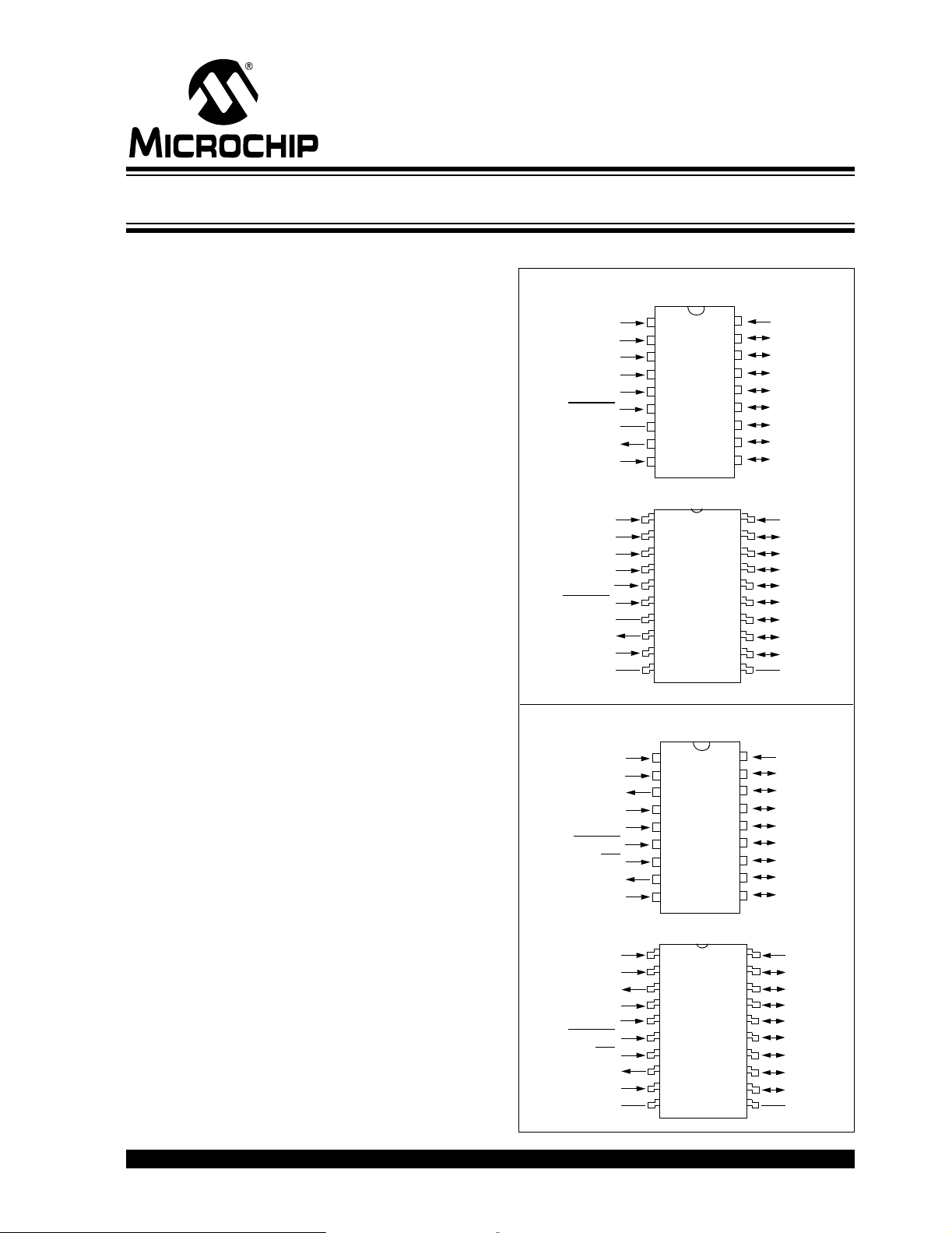
Packages
18-pin PDIP (300 mil)
18-pin SOIC (300 mil)
20-pin SSOP
Package Types
MCP23008
SCL
SDA
A2
A1
A0
RESET
NC
INT
V
SS
SCL
SDA
A2
A1
A0
RESET
NC
INT
VSS
N/C
MCP23S08
SCK
SI
SO
A1
A0
RESET
CS
INT
VSS
SCK
SI
SO
A1
A0
RESET
CS
INT
VSS
N/C
PDIP/SOIC
1
2
3
4
5
6
MCP23008
7
8
9
SSOP
1
2
3
4
5
6
7
MCP23008
8
9
10
PDIP/SOIC
1
2
3
4
5
6
MCP23S08
7
8
9
SSOP
1
2
3
4
5
6
7
8
9
10
18
17
16
15
14
13
12
11
10
20
19
18
17
16
15
14
13
12
11
18
17
16
15
14
13
12
11
10
20
19
18
17
16
15
14
MCP23S08
13
12
11
DD
V
GP7
GP6
GP5
GP4
GP3
GP2
GP1
GP0
V
GP7
GP6
GP5
GP4
GP3
GP2
GP1
GP0
N/C
DD
V
GP7
GP6
GP5
GP4
GP3
GP2
GP1
GP0
V
GP6
GP5
GP4
GP3
GP2
GP1
GP0
N/C
DD
DD
GP7
© 2005 Microchip Technology Inc. DS21919B-page 1
Page 2
MCP23008/MCP23S08
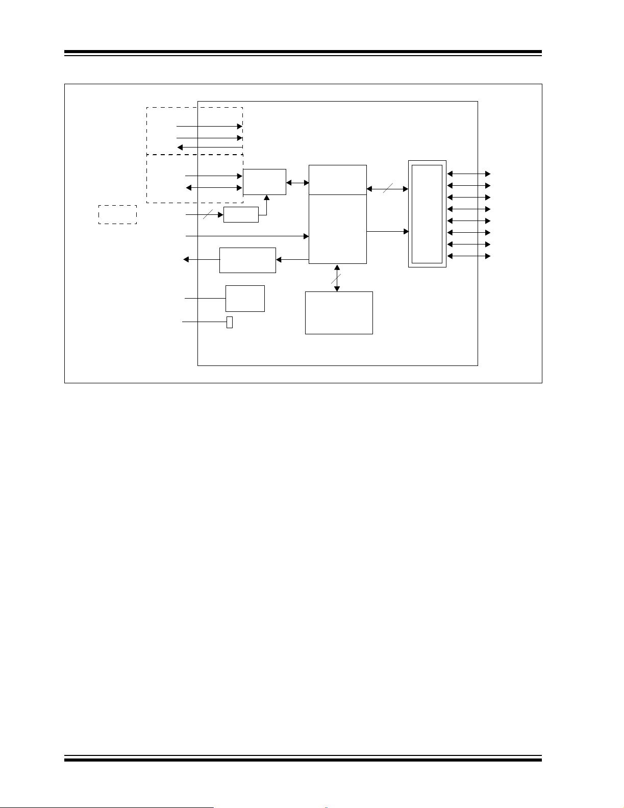
Block Diagram
MCP23S08
SCK
SI
SO
MCP23008
MCP23S08
A1:A0
SCL
SDA
A2:A0
RESET
INT
3
Serial
Interface
Decode
Interrupt
Logic
Serializer/
Deserializer
Control
8
GP0
8
GPIO
GP1
GP2
GP3
GP4
GP5
GP6
GP7
VDD
VSS
POR
Configuration/
Control
Registers
DS21919B-page 2 © 2005 Microchip Technology Inc.
Page 3
MCP23008/MCP23S08
1.0 DEVICE OVERVIEW
The MCP23X08 device provides 8-bit, general
purpose, parallel I/O expansion for I
applications. The two devices differ in the number of
hardware address pins and the serial interface:
2
• MCP23008 – I
• MCP23S08 – SPI interface; two address pins
The MCP23X08 consists of multiple 8-bit configuration
registers for input, output and polarity selection. The
system master can enable the I/Os as either inputs or
outputs by writi ng the I/O configur ation bits. The data
for each input or output is kept in the corresponding
Input or Output register. The polarity of the Input Port
register can be inverted with the Polarity Inversion
register . All registers ca n be read by the sy stem maste r.
C interface; three address pins
2
C bus or SPI
The interrupt output can be configured to activate
under two conditions (mutually exclusive):
1. When any input state differs from its
corresponding input port register state. This is
used to indicate to the system master that an
input state has changed.
2. When an input stat e differs from a preconfigure d
register value (DEFVAL register).
The Interrupt Capture register captures port values at
the time of the interrupt, thereby saving the condition
that caused the interrupt.
The Power-on Reset (POR) sets the registers to their
default values and initi ali zes the device state mach in e.
The hardware address pins are used to determine the
device address.
1.1 Pin Descriptions
TABLE 1-1: PINOUT DESCRIPTION
Pin
Name
SCL/SCK 1 1 I Serial clock input.
SDA/SI 2 2 I/O Serial data I/O (MCP23008)/Serial data input (MCP23S08).
A2/SO 3 3 I/O Hardware address input (MCP23008)/Serial data output (MCP23S08).
A1 4 4 I Hardware address input. Must be biased externally.
A0 5 5 I Hardware address input. Must be biased externally.
RESET
NC/CS 7 7 I No connect (MCP23008)/External chip select input (MCP23S08).
INT 8 8 O Interrupt output. Can be configured for active-high, active-low or open-drain.
SS 9 9 P Ground.
V
GP0 10 12 I/O Bidirectional I/O pin. Can be enabled for interrupt -on-change an d/or interna l weak
GP1 11 13 I/O Bidirectional I/O pin. Can be enabled for interrupt -on-change an d/or interna l weak
GP2 12 14 I/O Bidirectional I/O pin. Can be enabled for interrupt -on-change an d/or interna l weak
GP3 13 15 I/O Bidirectional I/O pin. Can be enabled for interrupt -on-change an d/or interna l weak
GP4 14 16 I/O Bidirectional I/O pin. Can be enabled for interrupt -on-change an d/or interna l weak
GP5 15 17 I/O Bidirectional I/O pin. Can be enabled for interrupt -on-change an d/or interna l weak
GP6 16 18 I/O Bidirectional I/O pin. Can be enabled for interrupt -on-change an d/or interna l weak
GP7 17 19 I/O Bidirectional I/O pin. Can be enabled for interrupt -on-change an d/or interna l weak
DD 18 20 P Power.
V
N/C 10, 1 1
PDIP/S
SSOP
OIC
6 6 I External reset input
Pin
Type
A2 must be biased externally.
pull-up resistor.
pull-up resistor.
pull-up resistor.
pull-up resistor.
pull-up resistor.
pull-up resistor.
pull-up resistor.
pull-up resistor.
Function
© 2005 Microchip Technology Inc. DS21919B-page 3
Page 4

MCP23008/MCP23S08
1.2 Power-on Reset (POR)
The on-chip P OR c ircui t ho lds the device in r eset unt il
DD has reached a high enough voltage to deactivate
V
the POR circuit (i.e., release the device from reset).
The maximum VDD rise time is specified in Section 2.0
“Electrical Characteristics”.
When the device exits the POR condition (releases
reset), device operating parameters (i.e., voltage,
temperature, serial bus frequen cy, etc.) must be met to
ensure proper operation.
1.3 Serial Interface
This block handles the functionality of the I2C
(MCP23008) or SPI (MCP23S08) interface protocol.
The MCP23X08 contains eleven registers that can be
addressed through the serial interface block (Table 1-2):
TABLE 1-2: REGISTER ADDRESSES
Address Access to:
00h IODIR
01h IPOL
02h GPINTEN
03h DEFVAL
04h INTCON
05h IOCON
06h GPPU
07h INTF
08h INTCAP (Read-only)
09h GPIO
0Ah OLAT
1.3.1 SEQUENTIAL OPERATION BIT
The Sequential Operation (SEQOP) bit (IOCON
register) controls the operation of the address pointer.
The address pointer can either be enabled (default) to
allow the address pointer to increment automatically
after each data transfer, or it can be disabled.
When operating in Sequential mode
(IOCON.SEQOP = 0), the address pointer automatically increments to the next address after each byte
is clocked.
When operating in Byte mode (IOCON.SEQOP = 1),
the MCP23X08 does not increment its address
counter after each byte during the data transfer. This
gives the ability to contin ually read the same address
by providing extra clocks (without additional control
bytes). This is useful for polling the GPIO register for
data changes.
1.3.2 I2C™ INTERFACE
1.3.2.1 I
The I2C Write operation includes the control byte and
register address sequence, as shown in the bottom of
Figure 1-1. This sequence is followed by eight bits of
data from the master and an Acknowledge (ACK) from
the MCP23008. The operation is ended with a STOP
or RESTART condition being generated by the master.
Data is written to the MCP23008 after every byte
transfer. If a STOP or RESTART condition is
generated during a data transfer, the data will not be
written to the MCP23008.
Byte writes and sequential writes are both supported
by the MCP23008. The MCP23008 increments its
address counter after each ACK during the data
transfer.
2
C Write Operation
1.3.2.2 I2C Read Operation
The I2C Read operation includes the control byte
sequence, as shown in the bottom of Figure 1-1. This
sequence is followed by another control byte (including the START condition and ACK) with the R/W bit
equal to a logic 1 (R/W = 1). The MCP23008 then
transmits the data contained in the addressed register.
The sequence is ended with the master generating a
STOP or RESTART condition.
1.3.2.3 I2C Sequential Write/Read
For sequential operations (Write or Read), instead of
transmitting a STOP or RESTART condition after the
data transfer , the master cl ocks the next byte pointe d to
by the address pointe r (see Section 1.3.1 “Sequ ential
Operation Bit” for details regarding sequential
operation control).
The sequence ends with the master sendin g a STOP or
REST AR T co ndi tio n.
The MCP23008 address pointer will roll over to
address zero after reaching the last register address.
Refer to Figure 1-1.
1.3.3 SPI™ INTERFACE
1.3.3.1 SPI Write Operation
The SPI Write opera tion is st arted by lowe ring CS . The
Write command (slave address with R/W bit cleared) is
then clocked into the dev ice. The opcod e is followed by
an address and at least one data byte.
1.3.3.2 SPI Read Operation
The SPI Read operation is st arted by lowe ring CS. The
SPI read command (slave address with R/W bit set) is
then clocked into the dev ice. The opcod e is followed by
an address, with at least one data byte being clocked
out of the device.
DS21919B-page 4 © 2005 Microchip Technology Inc.
Page 5
MCP23008/MCP23S08
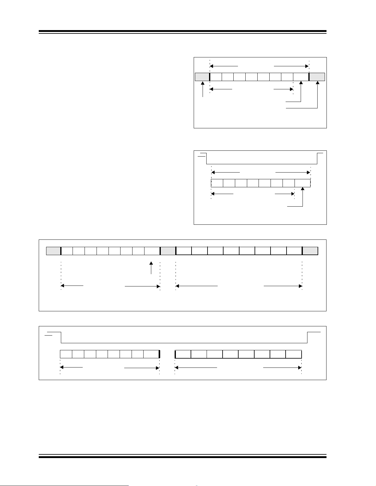
FIGURE 1-1: MCP23008 I2C™ DEVICE PROTOCOL
- START
S
- RESTART
SR
P
w
R
- STOP
- Write
- Read
OP
S P
- Device opcode
OP ADDR
W
DIN DIN
SR
SR WOP
OP
....
D
OUT
R
D
IN
....
....
DOUT
DIN
P
P
ADDR
DOUT
DIN
- Device address
- Data out from MCP23008
- Data into MCP23008
OP
S
Byte
Sequential
S WOP ADDR
S PWOP ADDR
P
R
SR R
SR OP
P
Byte and Sequential Write
Byte and Sequential Read
DOUT DOUT
W
DIN
DIN
OP
....
ADDR
....
D
P
DIN
OUT
D
P
DOUT
....
IN
....
DIN
P
P
D
D
OUT
OUT
....
P
DOUT
P
Byte
S
OP SR ROP
Sequential
OP SR R
S
1.3.3.3 SPI Sequential Write/Read
For sequential operations, instead of deselecting the
device by raising CS
pointed to by the address pointer.
The sequence ends by the raising of CS.
The MCP23S08 address pointer will roll over to
address zero after reaching the last register address.
© 2005 Microchip Technology Inc. DS21919B-page 5
, the master clocks the next byte
R
R
OP
1.4 Hardware Address Decoder
The hardware address pins are used to determine the
device address. To address a device, the corresponding address bits in the control byte must match the pin
state.
• MCP23008 has address pins A2, A1 and A0.
• MCP23S08 has address pins A1 and A0.
The pins must be biased externally.
Page 6
MCP23008/MCP23S08
1.4.1 ADDRESSING I2C DEVICES
(MCP23008)
The MCP23008 is a slave I2C device that supports 7-bit
slave addressing, with the read/write bit filling out the
control byte. The slave address contains fo ur fixed bits
and three user-defined hardware address bits (pins A2,
A1 and A0). Figure 1-2 shows the control byte format.
1.4.2 ADDRESSING SPI DEVICES
(MCP23S08)
The MCP23S08 is a slave SPI device. The slave
address contains five fixed bits and two user-defined
hardware address bits (pins A1 and A0), with the
read/write bit filling out the control byte. Figure 1-3
shows the control byte format.
FIGURE 1-2: I2C™ CONTROL BYTE
FORMAT
Control Byte
S 0 1 0 0 A2A1A0R/WACK
Slave Address
Start
bit
R/W = 0 = write
R/W = 1 = read
R/W bit
ACK bit
FIGURE 1-3: SPI™ CONTROL BYTE
FORMAT
CS
Control Byte
01000A1A0R/W
Slave Address
R/W bit
R/W = 0 = write
R/W = 1 = read
FIGURE 1-4: I
S0100A2A1A00ACKA7A6A5A4A3A2A1A0ACK
2
C™ ADDRESSING REGISTERS
R/W = 0
Device Opcode Register Address
The ACKs are provided by the MCP23008.
FIGURE 1-5: SPI™ ADDRESSING REGISTERS
CS
01000A1A0R/W A7A6A5A4A3A2A1A0
Device Opcode Register Address
DS21919B-page 6 © 2005 Microchip Technology Inc.
Page 7
MCP23008/MCP23S08
1.5 GPIO Port
The GPIO module contains the data port (GPIO),
internal pull up resistors and the Output Latches
(OLAT).
1.6 Configuration and Control Registers
The Configuration and Control blocks contain the
registers as shown in Table 1-3.
Reading the GPIO regi ster read s the va lue on th e port.
Reading the OLAT register only reads the OLAT, not
the actual value on the port.
Writing to the GPIO register actually causes a write to
the OLAT. Writing to the OLAT register forces the
associated output drivers to drive to the level in OLAT.
Pins configured as inpu ts turn of f the ass ociated outp ut
driver and put it in high-impedance.
TABLE 1-3: CONFIGURATION AND CONTROL REGISTERS
Register
Name
IODIR 00 IO7 IO6 IO5 IO4 IO3 IO2 IO1 IO0 1111 1111
IPOL 01 IP7 IP6 IP5 IP4 IP3 IP2 IP1 IP0 0000 0000
GPINTEN 02 G PINT7 GPINT6 GPINT5 GPINT4 GPINT3 GPINT2 GPINT1 GPINT0 0000 0000
DEFVAL 03 DEF7 DEF6 DEF5 DEF4 DEF3 DEF2 DEF1 DEF0 0000 0000
INTCON 04 IOC7 IOC6 IOC5 IOC4 IOC3 IOC2 IOC1 IOC0 0000 0000
IOCON 05
GPPU 06 PU7 PU6 PU5 PU4 PU3 PU2 PU1 PU0 0000 0000
INTF 07 INT7 INT6 INT5 INT4 INT3 INT2 INT1 INTO 0000 0000
INTCAP 08 ICP7 ICP6 ICP5 ICP4 ICP3 ICP2 ICP1 ICP0 0000 0000
GPIO 09 GP7 GP6 GP5 GP4 GP3 GP2 GP1 GP0 0000 0000
OLAT 0A OL7 OL6 OL5 OL4 OL3 OL2 OL1 OL0 0000 0000
Address
(hex)
bit 7 bit 6 bit 5 bit 4 bit 3 bit 2 bit 1 bit 0
— — SREAD DISSLW HAEN * ODR INTPOL — --00 000-
* Not used on the MCP23008.
POR/RST
value
© 2005 Microchip Technology Inc. DS21919B-page 7
Page 8
MCP23008/MCP23S08
1.6.1 I/O DIRECTION (IODIR) REGISTER
Controls the direction of the data I/O.
When a bit is set, the corresponding pin becomes an
input. When a bit is clear, the corresponding pin
becomes an output.
REGISTER 1-1: IODIR – I/O DIRECTION REGISTER (ADDR 0x00)
R/W-1 R/W-1 R/W-1 R/W-1 R/W-1 R/W-1 R/W-1 R/W-1
IO7 IO6 IO5 IO4 IO3 IO2 IO1 IO0
bit 7 bit 0
bit 7-0 IO7:IO0: These bits control the direction of data I/O <7:0>.
1 = Pin is configured as an input.
0 = Pin is configured as an output.
Legend:
R = Readable bit W = Writable bit U = Unimplemented bit, read as ‘0’
- n = Value at POR ‘1’ = Bit is set ‘0’ = Bit is cleared x = Bit is unknown
DS21919B-page 8 © 2005 Microchip Technology Inc.
Page 9
MCP23008/MCP23S08
1.6.2 INPUT POLARITY (IPOL) REGISTER
The IPOL register allows the user to configure the
polarity on the corresponding GPIO port bits.
If a bit is set, the corresponding GPIO register bit will
reflect the inverted va lue on the pin.
REGISTER 1-2: IPOL – INPUT POLARITY PORT REGISTER (ADDR 0x01)
R/W-0 R/W-0 R/W-0 R/W-0 R/W-0 R/W-0 R/W-0 R/W-0
IP7 IP6 IP5 IP4 IP3 IP2 IP1 IP0
bit 7 bit 0
bit 7-0 IP7:IP0: These bits control the polarity inversion of the input pins <7:0>.
1 = GPIO register bit will reflect the opposite logic state of the input pin.
0 = GPIO register bit will reflect the same logic state of the input pin.
Legend:
R = Readable bit W = Writable bit U = Unimplemented bit, read as ‘0’
- n = Value at POR ‘1’ = Bit is set ‘0’ = Bit is cleared x = Bit is unknown
© 2005 Microchip Technology Inc. DS21919B-page 9
Page 10

MCP23008/MCP23S08
1.6.3 INTERRUPT-ON-CHANGE
CONTROL (GPINTEN) REGISTER
The GPINTEN register controls the interrupt-onchange feature for each pin.
If a bit is set, the corresponding pin is enabled for
interrupt-on-change. The DEFVAL and INTCON
registers must also be configured if any pins are
enabled for interrupt-on-change.
REGISTER 1-3: GPINTEN – INTERRUPT-ON-CHANGE PINS (ADDR 0x02)
R/W-0 R/W-0 R/W-0 R/W-0 R/W-0 R/W-0 R/W-0 R/W-0
GPINT7 GPINT6 GPINT5 GPINT4 GPINT3 GPINT2 GPINT1 GPINT0
bit 7 bit 0
bit 7-0 GPINT7:GPINT0: General purpose I/O interrupt-on-change bits <7:0>.
1 = Enable GPIO input pin for interrupt-on-change event.
0 = Disable GPIO input pin for interrupt-on-change event.
Refer to INTCON and GPINTEN.
Legend:
R = Readable bit W = Writable bit U = Unimplemented bit, read as ‘0’
- n = Value at POR ‘1’ = Bit is set ‘0’ = Bit is cleared x = Bit is unknown
DS21919B-page 10 © 2005 Microchip Technology Inc.
Page 11
MCP23008/MCP23S08
1.6.4 DEFAULT COMPARE (DEFVAL)
REGISTER FOR INTERRUPT-ONCHANGE
The default comparison value is configured in the
DEFVAL register. If enabled (via GPINTEN and
INTCON) to compare against the DEFVAL register, an
opposite value on the associated pin will cause an
interrupt to occur .
REGISTER 1-4: DEFVAL – DEFAULT VALUE REGISTER (ADDR 0x03)
R/W-0 R/W-0 R/W-0 R/W-0 R/W-0 R/W-0 R/W-0 R/W-0
DEF7 DEF6 DEF5 DEF4 DEF3 DEF2 DEF1 DEF0
bit 7 bit 0
bit 7-0 DEF7:DEF0: These bits set the compare value for pin s configured for interrupt-on-ch ange from
defaults <7:0>. Refer to INTCON.
If the associated pin level is the opposite from the register bit, an interrupt occurs.
Refer to INTCON and GPINTEN.
Legend:
R = Readable bit W = Writable bit U = Unimplemented bit, read as ‘0’
- n = Value at POR ‘1’ = Bit is set ‘0’ = Bit is cleared x = Bit is unknown
© 2005 Microchip Technology Inc. DS21919B-page 11
Page 12
MCP23008/MCP23S08
1.6.5 INTERRUPT CONTROL (INTCON)
REGISTER
The INTCON register controls how the associated pin
value is compared for the interrupt-on-change feature.
If a bit is set, the corresponding I/O pin is compared
against the associated bit in the DEFVAL register. If a
bit value is clear, the corresponding I/O pin is
compared against the previous value.
REGISTER 1-5: INTCON – INTERRUPT-ON-CHANGE CONTROL REGISTER (ADDR 0x04)
R/W-0 R/W-0 R/W-0 R/W-0 R/W-0 R/W-0 R/W-0 R/W-0
IOC7 IOC6 IOC5 IOC4 IOC3 IOC2 IOC1 IOC0
bit 7 bit 0
bit 7-0 IOC7:IOC0: These bits control how the associated pin value is compared for interrupt-on-
change <7:0>.
1 = Controls how the associated pin value is compared for interrupt-on-change.
0 = Pin value is compared against the previous pin value.
Refer to INTCON and GPINTEN.
Legend:
R = Readable bit W = Writable bit U = Unimplemented bit, read as ‘0’
- n = Value at POR ‘1’ = Bit is set ‘0’ = Bit is cleared x = Bit is unknown
DS21919B-page 12 © 2005 Microchip Technology Inc.
Page 13

MCP23008/MCP23S08
1.6.6 CONFIGURATION (IOCON)
REGISTER
The IOCON register contains several bits for
configuring the device:
• The Sequential Operation (SEQOP) controls the
incrementing function of the address pointer. If
the address pointer is disabled, the address
pointer does not automatically increment after
each byte is clocked during a serial transfer. This
feature is useful when i t is desire d to c ontinu ously
poll (read) or modify (write) a register.
• The Slew Rate (DISSLW) bit controls the slew
rate function on the SDA pin. If enabled, the SDA
slew rate will be controlled when driving from a
high to a low.
• The Hardware Address Enable (HAEN) cont rol bit
enables/disables the hardware address pins (A2,
A1) on the MCP23S0 8. Thi s bit i s not u sed o n the
MCP23008. The addres s pins are a lways enable d
on the MCP23008.
• The Open-Drain (ODR) control bit
enables/disables the INT pin for open-drain
configuration.
• The Interrupt Polarity (INTPOL) control bit sets
the polarity of the INT pin. This bit is functional
only when the ODR bit is cleared, configuring the
INT pin as active push-pull.
REGISTER 1-6: IOCON – I/O EXPANDER CONFIGURATION REGISTER (ADDR 0x05)
U-0 U-0 R/W-0 R/W-0 R/W-0 R/W-0 R/W-0 U-0
— —
bit 7 bit 0
bit 7-6 Unimplemented: Read as ‘0’.
bit 5 SEQOP: Sequential Operation mode bit.
1 = Sequential operation disabled, address pointer does not increment.
0 = Sequential operation enabled, address pointer increments.
bit 4 DISSLW: Slew Rate control bit for SDA output.
1 = Slew rate disabled.
0 = Slew rate enabled.
bit 3 HAEN: Hardware Address Enable bit (MCP23S08 only).
Address pins are always enabled on MCP23008.
1 = Enables the MCP23S08 address pins.
0 = Disables the MCP23S08 address pins.
bit 2 ODR: This bit configures the INT pin as an open-drain output.
1 = Open-drain output (overrides the INTPOL bit).
0 = Active driver output (INTPOL bit sets the polarity).
bit 1 INTPOL: This bit sets the polarity of the INT output pin.
1 =Active-high.
0 =Active-low.
bit 0 Unimplemented: Read as ‘0’.
SEQOP DISSLW HAEN ODR INTPOL
—
Legend:
R = Readable bit W = Writable bit U = Unimplemented bit, read as ‘0’
- n = Value at POR ‘1’ = Bit is set ‘0’ = Bit is cleared x = Bit is unknown
© 2005 Microchip Technology Inc. DS21919B-page 13
Page 14

MCP23008/MCP23S08
1.6.7 PULL-UP RESISTOR
CONFIGURATION (GPPU)
REGISTER
The GPPU register control s the pull-up resistors for the
port pins. If a bit is set and the corresponding pin is
configured as an input, the corresponding port pin is
internally pulled up with a 100 kΩ resistor.
REGISTER 1-7: GPPU – GPIO PULL-UP RESISTOR REGISTER (ADDR 0x06)
R/W-0 R/W-0 R/W-0 R/W-0 R/W-0 R/W-0 R/W-0 R/W-0
PU7 PU6 PU5 PU4 PU3 PU2 PU1 PU0
bit 7 bit 0
bit 7-0 PU7:PU0: These bits control the weak pull-up resistors on each pin (when configured as an
input) <7:0>.
1 = Pull-up enabled.
0 = Pull-up disabled.
Legend:
R = Readable bit W = Writable bit U = Unimplemented bit, read as ‘0’
- n = Value at POR ‘1’ = Bit is set ‘0’ = Bit is cleared x = Bit is unknown
DS21919B-page 14 © 2005 Microchip Technology Inc.
Page 15

MCP23008/MCP23S08
1.6.8 INTERRUPT FLAG (INTF)
REGISTER
The INTF register reflects the interrupt condition on the
port pins of any pin that is enabled for interrupts via the
GPINTEN register. A ‘set’ bit indicates that the
associated pin caused the interrupt.
This register is ‘read-o nly’. W rites to this regis ter will be
ignored.
Note: INTF will always reflect the pin(s) that
have an interrupt condition. For example,
one pin causes a n interrup t to occur and is
captured in INTCAP and INF. If, before
clearing the interrupt, ano ther pin change s
which would normally cause an interrupt, it
will be reflected in INTF, but not INTCAP.
REGISTER 1-8: INTF – INTERRUPT FLAG REGISTER (ADDR 0x07)
R-0 R-0 R-0 R-0 R-0 R-0 R-0 R-0
INT7 INT6 INT5 INT4 INT3 INT2 INT1 INT0
bit 7 bit 0
bit 7-0 INT7:INT0: These bits reflect the interrupt condition on the port. Will reflect the change only if
interrupts are enabled (GPINTE N) <7:0>.
1 = Pin caused interrupt.
0 = Interrupt not pending.
Legend:
R = Readable bit W = Writable bit U = Unimplemented bit, read as ‘0’
- n = Value at POR ‘1’ = Bit is set ‘0’ = Bit is cleared x = Bit is unknown
© 2005 Microchip Technology Inc. DS21919B-page 15
Page 16

MCP23008/MCP23S08
1.6.9 INTERRUPT CAPTURE (INTCAP)
REGISTER
The INTCAP register captures the GPIO port value at
the time the interrupt occurred. The register is ‘readonly’ and is updated o nly when an in terrupt occurs. Th e
register will remain unchanged until the interrupt is
cleared via a read of INTCA P or GPIO.
REGISTER 1-9: INTCAP – INTERRUPT CAPTURED VALUE FOR PORT REGISTER
(ADDR 0x08)
R-x R-x R-x R-x R-x R-x R-x R-x
ICP7 ICP6 ICP5 ICP4 ICP3 ICP2 ICP1 ICP0
bit 7 bit 0
bit 7-0 ICP7:ICP0: These bits reflect the logic level on the port pins at the time of interrupt due to pin
change <7:0>.
1 = Logic-high.
0 = Logic-low.
Legend:
R = Readable bit W = Writable bit U = Unimplemented bit, read as ‘0’
- n = Value at POR ‘1’ = Bit is set ‘0’ = Bit is cleared x = Bit is unknown
DS21919B-page 16 © 2005 Microchip Technology Inc.
Page 17

MCP23008/MCP23S08
1.6.10 PORT (GPIO) REGISTER
The GPIO register reflects the value on the port.
Reading from this reg ister reads the port. Writin g to this
register modifies the Output Latch (OLAT) register.
REGISTER 1-10: GPIO – GENERAL PURPOSE I/O PORT REGISTER (ADDR 0x09)
R/W-0 R/W-0 R/W-0 R/W-0 R/W-0 R/W-0 R/W-0 R/W-0
GP7 GP6 GP5 GP4 GP3 GP2 GP1 GP0
bit 7 bit 0
bit 7-0 GP7:GP0: These bits reflect the logic level on the pins <7:0>.
1 = Logic-high.
0 = Logic-low.
Legend:
R = Readable bit W = Writable bit U = Unimplemented bit, read as ‘0’
- n = Value at POR ‘1’ = Bit is set ‘0’ = Bit is cleared x = Bit is unknown
© 2005 Microchip Technology Inc. DS21919B-page 17
Page 18

MCP23008/MCP23S08
1.6.11 OUTPUT LATCH REGISTER (OLAT)
The OLAT register provides access to the output
latches. A read from this regi ster results in a read of the
OLAT and not the port itself. A write to this register
modifies the output latches that modify the pins
configured as outputs.
REGISTER 1-11: OLAT – OUTPUT LATCH REGISTER 0 (ADDR 0x0A)
R/W-0 R/W-0 R/W-0 R/W-0 R/W-0 R/W-0 R/W-0 R/W-0
OL7 OL6 OL5 OL4 OL3 OL2 OL1 OL0
bit 7 bit 0
bit 7-0 OL7:OL0: These bits reflect the logic level on the output latch <7:0>.
1 = Logic-high.
0 = Logic-low.
Legend:
R = Readable bit W = Writable bit U = Unimplemented bit, read as ‘0’
- n = Value at POR ‘1’ = Bit is set ‘0’ = Bit is cleared x = Bit is unknown
DS21919B-page 18 © 2005 Microchip Technology Inc.
Page 19

MCP23008/MCP23S08
1.7 Interrupt Logic
The interrupt output pin will activate if an internal
interrupt occurs. The interrupt block is configured by
the following registers:
• GPINTEN – enables the individual inputs
• DEFVAL – holds the values that are compared
against the associated input port values
• INTCON – controls if the input values are
compared ag ainst DE FVAL or the previous value s
on the port
• IOCON (ODR and INPOL) – configures the INT
pin as push-pull, open-drain and active-level
Only pins configured as inputs can cause interrupts.
Pins configured as outputs have no affect on INT.
Interrupt activity on the po rt w i ll cau se th e p ort v al ue to
be captured and copied into INTCAP. The interrupt will
remain active until the INTCAP or GPIO register is
read. Writing to these registers will not affect the
interrupt.
The first interrupt event will cause the port contents to
be copied into the INTCAP register. Subsequent
interrupt conditions on the port will not cause an
interrupt to occur as long as the interrupt is not cleare d
by a read of INTCAP or GPIO.
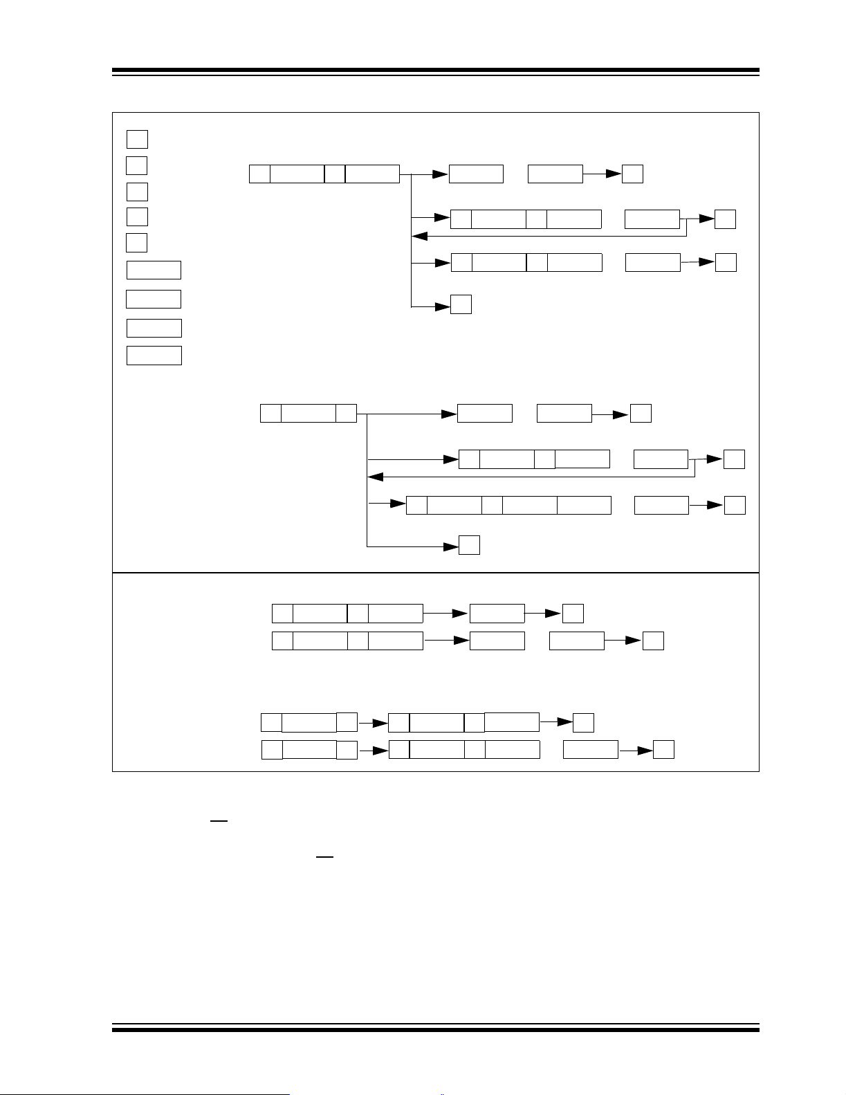
FIGURE 1-6: INTERRUPT-ON-PIN-
CHANGE
GPx
INT ACTIVE ACTIVE
Port value
is captured
into INTCAP
Read GPIU
or INTCAP
Port value
is captured
into INTCAP
FIGURE 1-7: INTERRUPT-ON-CHANGE
FROM REGISTER
DEFAULT
DEFVAL
76543210GP:
X X X X X 0 X X
GP2
1.7.1 INTERRUPT CONDITIONS
There are two possible configurations to cause
interrupts (configured via INTCON):
1. Pins configured for interrupt-on-pin-change
will cause an interrupt to occur if a pin changes
to the opposite state. The default state is reset
after an interrupt occurs. For example, an
interrupt occurs by an input changing from 1 to
0. The new initial state for the pin is a logic 0.
2. Pins configured for interrupt-on-change from
register value will cause an interrupt to occur if
the corresponding input pin differs from the
register bit. The i nterrupt condition will remain as
long as the condition exists, regardless if the
INTAP or GPIO is read.
See Figure 1-6 and Figure 1-7 for more information on
interrupt operations.
INT
Port value
is captured
into INTCAP
ACTIVE
ACTIVE
Read GPIU
or INTCAP
(INT clears only if interrupt
condition does not exist.)
© 2005 Microchip Technology Inc. DS21919B-page 19
Page 20

MCP23008/MCP23S08
NOTES:
DS21919B-page 20 © 2005 Microchip Technology Inc.
Page 21

MCP23008/MCP23S08
2.0 ELECTRICAL CHARACTERISTICS
Absolute Maximum Ratings †
Ambient temperature under bias.............................................................................................................-40°C to +125°C
Storage temperature.............................................................................................................................. -65°C to +150°C
Voltage on V
Voltage on all other pins with respect to V
Total power dissipation (Note) .............................................................................................................................700 mW
Maximum current out of V
Maximum current into V
Input clamp current, I
Output clamp current, I
Maximum output current sunk by any output pin ....................................................................................................25 mA
Maximum output current sourced by any output pin...............................................................................................25 mA
Note: Power dissipation is calculated as follows :
†
NOTICE: Stresses above those listed under “Absolute Maximum Ratings” may cause permanent damage to the
device. This is a stress rating onl y and funct ional ope ration of the device at tho se or any other co nditio ns above those
indicated in the operation listings of this specification is not implied. Exposure to maximum rating conditions for
extended periods may affect device reliability.
DD with respect to VSS ......................................................................................................... -0.3V to +5.5V
SS (except VDD) .............................................................-0.6V to (VDD + 0.6V)
SS pin...........................................................................................................................150 mA
DD pin..............................................................................................................................125 mA
IK (VI < 0 or VI > VDD)......................................................................................................................±20 mA
OK (VO < 0 or VO > VDD).............................................................................................................. ±20 mA
DIS = VDD x {IDD - ∑ IOH} + ∑ {(VDD-VOH) x IOH} + ∑(VOL x IOL)
P
© 2005 Microchip Technology Inc. DS21919B-page 21
Page 22

MCP23008/MCP23S08
2.1 DC Characteristics
Operating Conditions (unless otherwise indicated):
DC Characteristics
1.8V ≤ VDD ≤ 5.5V at -40°C ≤ TA ≤ +85°C (I-Temp)
4.5V ≤ V
DD ≤ 5.5V at -40°C ≤ TA ≤ +125°C (E-Temp) (Note 1)
Param
No.
D001 Supply Voltage V
D002 V
Characteristic Sym Min Typ Max Units Conditions
DD 1.8 — 5.5 V
DD Start Voltage to
POR —VSS —V
V
Ensure Power-on
Reset
D003 VDD Rise Rate to
SVDD 0.05 — — V/ms Design guidance only.
Ensure Power-on
Reset
D004 Supply Current I
D005 Standby current I
DD — — 1 mA SCL/SCK = 1 MHz
DDS ——1µA
— — 2 µA 4.5V - 5.5V @ +125°C
Input Low-Voltage
D030 A0, A1 (TTL buffer) V
D031 CS
, GPIO, SCL/SCK,
IL VSS —0.15VDD V
VSS —0.2VDD V
SDA, A2, RESET
(Schmitt Trigger)
Input High-Voltage
D040 A0, A1
IH 0.25 VDD + 0.8 — VDD V
V
(TTL buffer)
D041 CS
, GPIO, SCL/SCK,
0.8 VDD —VDD V For entire VDD range.
SDA, A2, RESET
(Schmitt Trigger)
Input Leakage Current
D060 I/O port pins I
IL ——±1µAVSS ≤ VPIN ≤ VDD
Output Leakage Current
D065 I/O port pins I
D070 GPIO weak pull-up
LO ——±1µAVSS ≤ VPIN ≤ VDD
IPU 40 75 1 15 µA VDD = 5V, GP Pins = VSS
current
Output Low-V o ltage
D080 GPIO V
OL ——0.6VIOL = 8.5 mA, VDD = 4.5V
INT — — 0.6 V I
SO, SDA — — 0.6 V I
SDA — — 0.8 V I
Output High-Voltage
D090 GPIO, INT, SO V
OH VDD – 0.7 — — V IOH = -3.0 mA, VDD = 4.5V
DD – 0.7 — — IOH = -400 µA, VDD = 1.8V
V
Capacitive Loading Specs on Output Pins
D101 GPIO, SO, INT C
D102 SDA C
IO ——50pF
B ——400pF
Note 1: This parameter is characterized, not 100% tested.
Not tested.
(Note 1)
–40°C ≤ TA ≤ +85°C
OL = 1.6 mA, VDD = 4.5V
OL = 3.0 mA, VDD = 1.8V
OL = 3.0 mA, VDD = 4.5V
DS21919B-page 22 © 2005 Microchip Technology Inc.
Page 23

MCP23008/MCP23S08
FIGURE 2-1: LOAD CONDITIONS FOR DEVICE TIMING SPECIFICATIONS
VDD
1kΩ
SCL and
SDA pin
MCP23008
135 pF
Pin
FIGURE 2-2: RESET AND DEVICE RESET TIMER TIMING
VDD
RESET
30
Internal
RESET
34
32
50 pF
Output pin
© 2005 Microchip Technology Inc. DS21919B-page 23
Page 24

MCP23008/MCP23S08
TABLE 2-1: DEVICE RESET SPECIFICATIONS
Operating Conditions (unless otherwise indicated):
AC Characteristics
1.8V ≤ VDD ≤ 5.5V at -40°C ≤ TA ≤ +85°C (I-Temp)
4.5V ≤ V
DD ≤ 5.5V at -40°C ≤ TA ≤ +125°C (E-Temp) (Note 1)
Param
No.
30 RESET
32 Device Active After Reset
34 Output High-Impedance
Note 1: This parameter is characterized, not 100% tested.
FIGURE 2-3: I
SCL
SDA
Characteristic Sym Min T yp
Pulse Width
(Low)
high
From RESET
90
Low
2
C™ BUS START/STOP BITS TIMING
START
Condition
TRSTL1 — — µs
HLD —TBDµsVDD = 5.0V
T
T
IOZ ——1µs
91
(1)
Max Units Conditions
92
STOP
Condition
93
FIGURE 2-4: I
SCL
SDA
In
SDA
Out
2
C™ BUS DATA TIMING
103
90
91 92
109
100
106
101
107
109
102
110
DS21919B-page 24 © 2005 Microchip Technology Inc.
Page 25

MCP23008/MCP23S08
TABLE 2-2: I2C™ BUS DATA REQUIREMENTS (SLAVE MODE)
Operating Conditions (unless otherwise indica ted):
I2C™ AC Characteristics
1.8V ≤ V
4.5V ≤ V
R
Param
Characteristic Sym Min Typ Max Units Conditions
No.
100 Clock High Time: THIGH
100 kHz mode 4.0 — — µs 1.8V – 5.5V (I-Temp)
400 kHz mode 0.6 — — µs 2.7V – 5.5V (I-Temp)
1.7 MHz mode 0.12 — — µs 4.5V – 5.5V (E-Temp)
101 Clock Low Time: T
100 kHz mode 4.7 — — µs 1.8V – 5.5V (I-Temp)
400 kHz mode 1.3 — — µs 2.7V – 5.5V (I-Temp)
1.7 MHz mode 0.32 — — µs 4.5V – 5.5V (E-Temp)
102 SDA and SCL Rise Time: T
100 kHz mode — — 1000 ns 1.8V – 5.5V (I-Temp)
(Note 1)
400 kHz mode 20 + 0.1 CB
1.7 MHz mode 20 — 160 ns 4.5V – 5.5V (E-Temp)
103 SDA and SCL Fall Time: TF
100 kHz mode — — 300 ns 1.8V – 5.5V (I-Temp)
(Note 1)
400 kHz mode 20 + 0.1 C
1.7 MHz mode 20 — 80 ns 4.5V – 5.5V (E-Temp)
90 START Condition Setup Time: T
100 kHz mode 4.7 — — µs 1.8V – 5.5V (I-Temp)
400 kHz mode 0.6 — — µs 2.7V – 5.5V (I-Temp)
1.7 MHz mode 0.16 — — µs 4.5V – 5.5V (E-Temp)
91 START Condition Hold Time: T
100 kHz mode 4.0 — — µs 1.8V – 5.5V (I-Temp)
400 kHz mode 0.6 — — µs 2.7V – 5.5V (I-Temp)
1.7 MHz mode 0.16 — — µs 4.5V – 5.5V (E-Temp)
106 Data Input Hold Time: T
100 kHz mode 0 — 3.45 µs 1.8V – 5.5V (I-Temp)
400 kHz mode 0 — 0.9 µs 2.7V – 5.5V (I-Temp)
1.7 MHz mode 0 — 0.15 µs 4.5V – 5.5V (E-Temp)
107 Data Input Setup Time: T
100 kHz mode 250 — — ns 1.8V – 5.5V (I-Temp)
400 kHz mode 100 — — ns 2.7V – 5.5V (I-Temp)
1.7 MHz mode 0.01 — — µs 4.5V – 5.5V (E-Temp)
92 STOP Condition Setup Time: T
100 kHz mode 4.0 — — µs 1.8V – 5.5V (I-Temp)
400 kHz mode 0.6 — — µs 2.7V – 5.5V (I-Temp)
1.7 MHz mode 0.16 — — µs 4.5V – 5.5V (E-Temp)
Note 1: This parameter is characterized, not 100% tested.
B is specified to be from 10 to 400 pF.
2: C
DD ≤ 5.5V at -40°C ≤ TA ≤ +85°C (I-Temp)
DD ≤ 5.5V at -40°C ≤ TA ≤ +125°C (E-Temp) (Note 1)
PU (SCL, SDA) = 1 kΩ, CL (SCL, SDA) = 135 pF
LOW
R
(2)
— 300 ns 2.7V – 5.5V (I-Temp)
(2)
B
— 300 ns 2.7V – 5.5V (I-Temp)
SU:STA
HD:STA
HD:DAT
SU:DAT
SU:STO
© 2005 Microchip Technology Inc. DS21919B-page 25
Page 26

MCP23008/MCP23S08
TABLE 2-2: I2C™ BUS DATA REQUIREMENTS (SLAVE MODE) (CONTINUED)
Operating Conditions (unless otherwise indica ted):
I2C™ AC Characteristics
1.8V ≤ V
4.5V ≤ V
R
Param
Characteristic Sym Min Typ Max Units Conditions
No.
109 Output Valid From Clock: TAA
100 kHz mode — — 3.45 µs 1.8V – 5.5V (I-Temp)
400 kHz mode — — 0.9 µs 2.7V – 5.5V (I-Temp)
1.7 MHz mode — — 0.18 µs 4.5V – 5.5V (E-Temp)
110 Bus Free Time: T
100 kHz mode 4.7 — — µs 1.8V – 5.5V (I-Temp)
400 kHz mode 1.3 — — µs 2.7V – 5.5V (I-Temp)
1.7 MHz mode N/A — N/A µs 4.5V – 5.5V (E-Temp)
Bus Capacitive Loading: C
100 kHz and 400 kHz — — 400 pF (Note 1)
1.7 MHz — — 100 pF (Note 1)
Input Filter Spike
Suppression: (SDA and SCL)
100 kHz and 400 kHz — — 50 ns
1.7 MHz — — 10 ns Spike suppression off
Note 1: This parameter is characterized, not 100% tested.
2: CB is specified to be from 10 to 400pF.
DD ≤ 5.5V at -40°C ≤ TA ≤ +85°C (I-Temp)
DD ≤ 5.5V at -40°C ≤ TA ≤ +125°C (E-Temp) (Note 1)
PU (SCL, SDA) = 1 kΩ, CL (SCL, SDA) = 135 pF
BUF
B
SP
T
FIGURE 2-5: SPI™ INPUT TIMING
CS
1
4
MSb in
5
high-impedance
SCK
SO
Mode 1,1
Mode 0,0
SI
3
11
6
7
2
LSb in
10
DS21919B-page 26 © 2005 Microchip Technology Inc.
Page 27

FIGURE 2-6: SPI™ OUTPUT TIMING
CS
MCP23008/MCP23S08
SCK
SO
8
12
MSb out
SI
9
13
don’t care
TABLE 2-3: SPI™ INTERFACE AC CHARACTERISTICS
Operating Conditions (unless otherwise indica ted):
SPI™ Interface AC Characteristics
Param
No.
Characteristic Sym Min Typ Max Units Conditions
Clock Frequency F
1CS
2CS
3CS
Setup Time TCSS 50 — — ns
Hold Time TCSH 100 — — ns 1.8V – 5.5V (I-Temp)
Disable Time TCSD 100 — — ns 1.8V – 5.5V (I-Temp)
4 Data Setup Time T
5Data Hold Time T
6CLK Rise Time T
7CLK Fall Time T
8Clock High Time T
Note 1: This parameter is characterized, not 100% tested.
V = 90 ns (max) when address pointer rolls over from address 0x0A to 0x00.
2: T
1.8V ≤ VDD ≤ 5.5V at -40°C ≤ TA ≤ +85°C (I-Temp)
4.5V ≤ V
DD ≤ 5.5V at -40°C ≤ TA ≤ +125°C (E-Temp) (Note 1)
CLK — — 5 MHz 1.8V – 5.5V (I-Temp)
— — 10 MHz 2.7V – 5.5V (I-Temp)
— — 10 MHz 4.5V – 5.5V (E-Temp)
50 — — ns 2.7V – 5.5V (I-Temp)
50 — — ns 4.5V – 5.5V (E-Temp)
50 — — ns 2.7V – 5.5V (I-Temp)
50 — — ns 4.5V – 5.5V (E-Temp)
SU 20 — — ns 1.8V – 5.5V (I-Temp)
10 — — ns 2.7V – 5.5V (I-Temp)
10 — — ns 4.5V – 5.5V (E-Temp)
HD 20 — — ns 1.8V – 5.5V (I-Temp)
10 — — ns 2.7V – 5.5V (I-Temp)
10 — — ns 4.5V – 5.5V (E-Temp)
R ——2 µsNote 1
F ——2 µsNote 1
HI 90 — — ns 1.8V – 5.5V (I-Temp)
45 — — ns 2.7V – 5.5V (I-Temp)
45 — — ns 4.5V – 5.5V (E-Temp)
2
Mode 1,1
Mode 0,0
14
LSb out
© 2005 Microchip Technology Inc. DS21919B-page 27
Page 28

MCP23008/MCP23S08
TABLE 2-3: SPI™ INTERFACE AC CHARACTERISTICS (CONTINUED)
Operating Conditions (unless otherwise indica ted):
SPI™ Interface AC Characteristics
1.8V ≤ VDD ≤ 5.5V at -40°C ≤ TA ≤ +85°C (I-Temp)
4.5V ≤ V
DD ≤ 5.5V at -40°C ≤ TA ≤ +125°C (E-Temp) (Note 1)
Param
No.
Characteristic Sym Min Typ Max Units Conditions
9 Clock Low Time TLO 90 — — ns 1.8V – 5.5V (I-Temp)
45 — — ns 2.7V – 5.5V (I-Temp)
45 — — ns 4.5V – 5.5V (E-Temp)
10 Clock Delay Time T
1 1 Clock Enable Time T
12 Output Valid from Clock Low T
CLD 50 — — ns
CLE 50 — — ns
V — — 90 ns 1.8V – 5.5V (I-Temp)
— — 45 ns 2.7V – 5.5V (I-Temp)
— — 45 ns 4.5V – 5.5V (E-Temp)
13 Output Hold Time T
14 Output Disa ble Time T
HO 0——ns
DIS — — 100 ns
Note 1: This parameter is characterized, not 100% tested.
2: T
V = 90 ns (max) when address pointer rolls over from address 0x0A to 0x00.
FIGURE 2-7: GPIO AND INT TIMING
SCL/SCK
SDA/SI
In
D1
D0
LSb of data byte zero
during a write or read
command, depending
on parameter.
50
GPn
Output
Pin
51
INT
Pin
INT pin active
GPn
Input
Pin
Register
Loaded
DS21919B-page 28 © 2005 Microchip Technology Inc.
inactive
53
52
Page 29

TABLE 2-4: GP AND INT PINS
AC Characteristics
MCP23008/MCP23S08
Operating Conditions (unless otherwise indica ted):
1.8V ≤ VDD ≤ 5.5V at -40°C ≤ TA ≤ +85°C (I-Temp)
4.5V ≤ V
DD ≤ 5.5V at -40°C ≤ TA ≤ +125°C (E-Temp) (Note 1)
Param
No.
50 Serial data to output valid TGPOV ——500ns
51 Interrupt pin disable time T
52 GP input change to register
53 IOC event to INT active TGPINT ——500ns
Note 1: This parameter is characterized, not 100% tested
Characteristic Sym Min Typ Max Units Conditions
INTD ——450ns
T
GPIV ——450ns
valid
Glitch Filter on GP Pins T
GLITCH ——150ns
© 2005 Microchip Technology Inc. DS21919B-page 29
Page 30

MCP23008/MCP23S08
NOTES:
DS21919B-page 30 © 2005 Microchip Technology Inc.
Page 31

3.0 PACKAGING INFORMATION
3.1 Package Marking Information
MCP23008/MCP23S08
18-Lead PDIP (300 mil)
XXXXXXXXXXXXXXXXX
XXXXXXXXXXXXXXXXX
YYWWNNN
18-Lead SOIC (300 mil)
XXXXXXXXXXXX
XXXXXXXXXXXX
XXXXXXXXXXXX
YYWWNNN
20-Lead SSOP
Example:
Example:
Example:
MCP23008-E/P^^
0434256
MCP23008
E/SO^^
3
e
0434256
3
e
XXXXXXXXXXXX
XXXXXXXXXXXX
YYWWNNN
Legend: XX...X Customer-specific information
Y Year code (last digit of calendar year)
YY Year code (last 2 digits of calendar year)
WW Week code (week of January 1 is week ‘01’)
NNN Alphanumeric trac ea bil ity code
3
e
Pb-free JEDEC designator for Matte Tin (Sn)
* This package is Pb- free. The Pb-free JEDEC designator ( )
can be found on the outer packaging for this package.
Note: In the event the full Microchip part nu mber ca nnot be m arked o n one lin e, it will
be carried over to the next line, thus limiting the number of available
characters for customer-specific information.
MCP23S08
XXXXXXXXXXXX
ESS^^
0434256
3
e
3
e
© 2005 Microchip Technology Inc. DS21919B-page 31
Page 32

MCP23008/MCP23S08
18-Lead Plastic Dual In-line (P) – 300 mil (PDIP)
E1
D
2
n
1
α
E
A
c
A1
β
eB
Number of Pins
Pitch
Lead Thickness
Mold Draft Angle Top
Mold Draft Angle Bottom
* Controlling Parameter
§ Significant Characteristic
Notes:
Dimensions D and E1 do not include mold flash or protrusions. Mold flash or protrusions shall not exceed
.010” (0.254mm) per side.
JEDEC Equivalent: MS-001
Drawing No. C04-007
n
p
c
α
β
.100
B1
B
0.38.015A1Base to Seating Plane
p
MILLIMETERSINCHES*Units
2.54
A2
L
MAXNOMMINMAXNOMMINDimension Limits
1818
4.323.943.56.170.155.140ATop to Seating Plane
3.683.302.92.145.130.115A2Molded Package Thickness
8.267.947.62.325.313.300EShoulder to Shoulder Wid th
6.606.356.10.260.250.240E1Molded Package Width
22.9922.8022.61.905.898.890DOverall Length
3.433.303.18.135.130.125LTip to Seating Plane
0.380.290.20.015.012.008
1.781.461.14.070.058.045B1Upper Lead Width
0.560.460.36.022.018.014BLower Lead Width
10.929.407.87.430.370.310eBOverall Row Spacing §
1510515105
1510515105
DS21919B-page 32 © 2005 Microchip Technology Inc.
Page 33

MCP23008/MCP23S08
18-Lead Plastic Small Outline (SO) – Wide, 300 mil (SOIC)
p
B
n
45°
c
β
E1
E
D
2
1
h
A
φ
L
A1
α
A2
MILLIMETERSINCHES*Units
Number of Pins
Pitch
Foot Angle
Lead Thickness
Mold Draft Angle Top
Mold Draft Angle Bottom
* Controlling Parameter
§ Significant Characteristic
Notes:
Dimensions D and E1 do not include mold flash or protrusions. Mold flash or protrusions shall not exceed
.010” (0.254mm) per side.
JEDEC Equivalent: MS-013
Drawing No. C04-051
n
p
φ
c
α
β
048048
1.27.050
MAXNOMMINMAXNOMMINDimension Limits
1818
2.642.502.36.104.099.093AOverall Height
2.392.312.24.094.091.088A2Molded Package Thickness
0.300.200.10.012.008.004A1Standoff §
10.6710.3410.01.420.407.394EOverall Width
7.597.497.39.299.295.291E1Molded Package Width
11.7311.5311.33.462.454.446DOverall Length
0.740.500.25.029.020.010hChamfer Distance
1.270.840.41.050.033.016LFoot Length
0.300.270.23.012.011.009
0.510.420.36.020.017.014BLead Width
1512015120
1512015120
© 2005 Microchip Technology Inc. DS21919B-page 33
Page 34

MCP23008/MCP23S08
20-Lead Plastic Shrink Small Outline (SS) – 209 mil Body, 5.30 mm (SSOP)
E
p
E1
D
B
n
c
Number of Pins
Pitch
Lead Thickness
Foot Angle
*Controlling Parameter
Notes:
Dimensions D and E1 do not include mold flash or protrusions. Mold flash or protrusions
shall not exceed .010" (0.254mm) per side.
n
p
c
f
2
1
A
f
L
A1
A2
MILLIMETERS*INCHESUnits
MAXNOMMINMAXNOMMINDimension Limits
2020
0.65.026
2.00--.079--AOverall Height
1.851.751.65.073.069.065A2Molded Package Thickness
--0.05--.002A1Standoff
8.207.807.40.323.307.291EOverall Width
5.605.305.00.220.209.197E1Molded Package Width
7.507.20.295.289.283.272DOverall Length
0.950.750.55.037.030.022LFoot Length
0.25-0.09.010-.004
8°4°0°8°4°0°
0.38-0.22.015-.009BLead Width
JEDEC Equivalent: MO-150
Drawing No. C04-072
Revised 11/03/03
DS21919B-page 34 © 2005 Microchip Technology Inc.
Page 35

APPENDIX A: REVISION HISTORY
Revision B (February 2005)
The following is the list of modifications:
1. Section 1.6 “Configuration and Control Reg-
isters”. Added Hardware Address Enable
(HAEN) bit to Table 1-3.
2. Section 1.6.6 “Configu ration (IOC ON) Regis-
ter”. Added Hard ware Address Enable (HAE N)
bit to Register 1-6.
Revision A (December 2004)
Original Release of this Document.
MCP23008/MCP23S08
© 2005 Microchip Technology Inc. DS21919B-page 35
Page 36

MCP23008/MCP23S08
NOTES:
DS21919B-page 36 © 2005 Microchip Technology Inc.
Page 37

MCP23008/MCP23S08
PRODUCT IDENTIFICATION SYSTEM
To order or obtain information, e.g., on pricing or delivery , refer to the factory or the listed sales office.
PART NO. X /XX
Device
Device MCP23008: 8-Bit I/O Expander w/ I2C™ Interface
Temperature
Range
Package P = Plastic DIP (300 mil Body), 18-Lead
–
Range
MCP23008T: 8-Bit I/O Expander w/ I
MCP23S08: 8-Bit I/O Expander w/ SPI™ Interface
MCP23S08T: 8-Bit I/O Expander w/ SPI Interface
E= -40°C to +125°C (Extended) *
* While these devices are only offered in the “E”
temperature range, the device will operate at different
voltages and temperatures as identified in the
Section 2.0 “Electrical Characteristics”.
SO = Plastic SOIC (300 mil Body), 18-Lead
SS = SSOP, (209 mil Body, 5.30 mm), 20-Lead
PackageTemperature
(Tape and Reel)
(Tape and Reel)
2
C Interface
Examples:
a) MCP23008-E/P: Extended Temp.,
b) MCP23008-E/SO: Extended Temp.,
c) MCP23008T-E/SO: Tape and Reel,
d) MCP23008-E/SS: Extended Temp.,
e) MCP23008T-E/SS: Tape and Reel,
a) MCP23S08-E/P: Extended Temp.,
b) MCP23S08-E/SO: Extended Temp.,
c) MCP23S08T-E/SO: Tape and Reel,
d) MCP23S08-E/SS: Extended Temp.,
e) MCP23S08T-E/SS: Tape and Reel,
18LD PDIP package.
18LD SOIC package.
Extended T emp.,
18LD SOIC package.
20LD SSOP package.
Extended T emp.,
20LD SSOP package.
18LD PDIP package.
18LD SOIC package.
Extended T emp.,
18LD SOIC package.
20LD SSOP package.
Extended T emp.,
20LD SSOP package.
© 2005 Microchip Technology Inc. DS21919B-page 37
Page 38

MCP23008/MCP23S08
NOTES:
DS21919B-page 38 © 2005 Microchip Technology Inc.
Page 39

Note the following details of the code protection feature on Microchip devices:
• Microchip products meet the specification contained in their particular Microchip Data Sheet.
• Microchip believes that its family of products is one of the most secure families of its kind on the market today, when used in the
intended manner and under normal conditions.
• There are dishonest and possibly illegal methods used to breach the code protection feature. All of these methods, to our
knowledge, require using the Microchip products in a manner outside the operating specifications contained in Microchip’s Data
Sheets. Most likely, the person doing so is engaged in theft of intellectual property.
• Microchip is willing to work with the customer who is concerned about the integrity of their code.
• Neither Microchip nor any other semiconductor manufacturer can guarantee the security of their code. Code protection does not
mean that we are guaranteeing the product as “unbreakable.”
Code protection is constantly evolving. We at Microchip are com mitted to continuously improving the code protect ion f eatures of our
products. Attempts to break Microchip’s code protection feature may be a violation of the Digit al Mill ennium Copyright Act. If such acts
allow unauthorized access to your software or other copyrighted work, you may have a right to sue for relief under that Act.
Information contained in this publication regarding device
applications and the like is provided only for your convenience
and may be superseded by updates. It is your responsibility to
ensure that your application meets with your specifications.
MICROCHIP MAKES NO REPRESENTATIONS OR WARRANTIES OF ANY KIND WHETHER EXPRESS OR IMPLIED,
WRITTEN OR ORAL, STATUTORY OR OTHERWISE,
RELATED TO THE INFORMATION, INCLUDING BUT NOT
LIMITED TO ITS CONDITION, QUALITY, PERFORMANCE,
MERCHANTABILITY OR FITNESS FOR PURPOSE.
Microchip disclaims all liability arising from this information and
its use. Use of M icrochip’s prod ucts as critical components in
life support systems is not authorized except with express
written approval by Microchip. No licenses are conveyed,
implicitly or otherwise, under any Microchip intellectual property
rights.
Trademarks
The Microchip name and logo, the Microchip logo, Accuron,
dsPIC, K
EELOQ, microID, MPLAB, PIC, PICmicro, PICSTART,
PRO MATE, PowerSmart, rfPIC, and SmartShunt are
registered trademarks of Microchip Technology Incorporated
in the U.S.A. and other countries.
AmpLab, FilterLab, Migratable Memory, MXDEV, MXLAB,
PICMASTER, SEEVAL, SmartSensor and The Embedded
Control Solutions Company are registered trademarks of
Microchip Technology Incorporated in the U.S.A.
Analog-for-the-Digital Age, Application Maestro, dsPICDEM,
dsPICDEM.net, dsPICworks, ECAN, ECONOMONITOR,
FanSense, FlexROM, fuzzyLAB, In-Circuit Serial
Programmin g, IC SP, ICEPIC, MPASM, MPLIB, MPLIN K,
MPSIM, PICkit, PICDEM, PICDEM.net, PICLAB, PICtail,
PowerCal, PowerInfo, PowerMate, PowerTool, rfLAB,
rfPICDEM, Select Mode, Smart Serial, SmartT el, Total
Endurance and WiperLock are trademarks of Microchip
Technology Incorporated in the U.S.A. and other countries.
SQTP is a service mark of Microchip T echnology Incorporated
in the U.S.A.
All other trademarks mentioned herein are property of their
respective companies.
© 2005, Microchip Technology Incorporated, Printed in the
U.S.A., All Rights Reserved.
Printed on recycled paper.
Microchip received ISO/TS-16949:2002 quality system certification for
its worldwide headquarters, design and wafer fabrication facilities in
Chandler and Tempe, Arizona and Mountain View, California in
October 2003. The Company’s quality system processes and
procedures are for its PICmicro
devices, Serial EEPROMs, microperipherals, nonvolatile memory and
analog products. In addition, Microchip’s quality system for the design
and manufacture of development systems is ISO 9001:2000 certified.
®
8-bit MCUs, KEELOQ
®
code hopping
© 2005 Microchip Technology Inc. DS21919B-page 39
Page 40

WORLDWIDE SALES AND SERVICE
AMERICAS
Corporate Office
2355 West Chandler Blvd.
Chandler, AZ 85224-6199
Tel: 480-792-7200
Fax: 480-792-7277
Technical Support:
http://support.microchip.com
Web Address:
www.microchip.com
Atlanta
Alpharetta, GA
Tel: 770-640-0034
Fax: 770-640-0307
Boston
Westford, MA
Tel: 978-692-3848
Fax: 978-692-3821
Chicago
Itasca, IL
Tel: 630-285-0071
Fax: 630-285-0075
Dallas
Addison, TX
Tel: 972-818-7423
Fax: 972-818-2924
Detroit
Farmington Hills, MI
Tel: 248-538-2250
Fax: 248-538-2260
Kokomo
Kokomo, IN
Tel: 765-864-8360
Fax: 765-864-8387
Los Angeles
Mission Viejo, CA
Tel: 949-462-9523
Fax: 949-462-9608
San Jose
Mountain View, CA
Tel: 650-215-1444
Fax: 650-961-0286
Toronto
Mississauga, Ontario,
Canada
Tel: 905-673-0699
Fax: 905-673-6509
ASIA/PACIFIC
Australia - Sydney
Tel: 61-2-9868-6733
Fax: 61-2-9868-6755
China - Beijing
Tel: 86-10-8528-2100
Fax: 86-10-8528-2104
China - Chengdu
Tel: 86-28-8676-6200
Fax: 86-28-8676-6599
China - Fuzhou
Tel: 86-591-8750-3506
Fax: 86-591-8750-3521
China - Hong Kong SAR
Tel: 852-2401-1200
Fax: 852-2401-3431
China - Shanghai
Tel: 86-21-5407-5533
Fax: 86-21-5407-5066
China - Shenyang
Tel: 86-24-2334-2829
Fax: 86-24-2334-2393
China - Shenzhen
Tel: 86-755-8203-2660
Fax: 86-755-8203-1760
China - Shunde
Tel: 86-757-2839-5507
Fax: 86-757-2839-5571
China - Qingdao
Tel: 86-532-502-7355
Fax: 86-532-502-7205
ASIA/PACIFIC
India - Bangalore
Tel: 91-80-2229-0061
Fax: 91-80-2229-0062
India - New Delhi
Tel: 91-11-5160-8631
Fax: 91-11-5160-8632
Japan - Kanagawa
Tel: 81-45-471- 6166
Fax: 81-45-471-6122
Korea - Seoul
Tel: 82-2-554-7200
Fax: 82-2-558-5932 or
82-2-558-5934
Singapore
Tel: 65-6334-8870
Fax: 65-6334-8850
Taiwan - Kaohsiung
Tel: 886-7-536-4818
Fax: 886-7-536-4803
Taiwan - Taipei
Tel: 886-2-2500-6610
Fax: 886-2-2508-0102
Taiwan - Hsinchu
Tel: 886-3-572-9526
Fax: 886-3-572-6459
EUROPE
Austria - Weis
Tel: 43-7242-2244-399
Fax: 43-7242-2244-393
Denmark - Ballerup
Tel: 45-4450-2828
Fax: 45-4485-2829
France - Massy
Tel: 33-1-69-53-63-20
Fax: 33-1-69-30-90-79
Germany - Ismaning
Tel: 49-89-627-144-0
Fax: 49-89-627-144-44
Italy - Milan
Tel: 39-0331-742611
Fax: 39-0331-466781
Netherlands - Drunen
Tel: 31-416-690399
Fax: 31-416-690340
England - Berkshire
Tel: 44-118-921-5869
Fax: 44-118-921-5820
10/20/04
DS21919B-page 40 © 2005 Microchip Technology Inc.
 Loading...