

Page 1
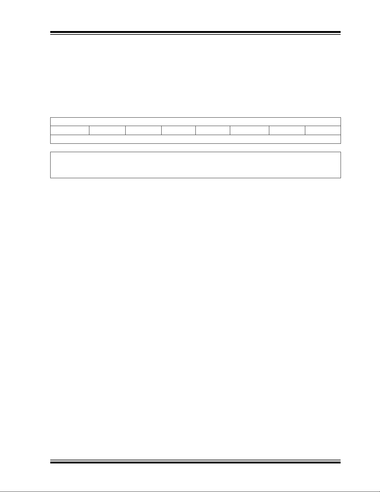
MCP23008/MCP23S08
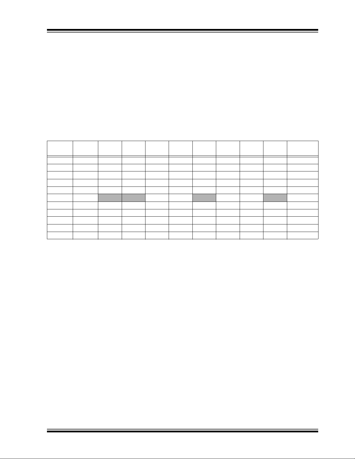
GP0
GP1
GP2
GP3
GP4
GP5
GP6
GP7
Serial
Control
GPIO
SCL
SDA
RESET
INT
8
Configuration/
8
A2:A0
3
Control
Registers
Serializer/
Deserializer
Interrupt
Logic
VDD
VSS
POR
Decode
Interface
SCK
SI
SO
MCP23S08
MCP23008
A1:A0
MCP23S08
8-Bit I/O Expander with Serial Interface
Features
• 8-bit remote bidirectional I/O port
- I/O pins default to input
• High-speed I
- 100 kHz
- 400 kHz
-1.7MHz
• High-speed SPI interface (MCP23S08)
-10MHz
• Hardware address pins
- Three for the MCP23008 to allow up to eight
devices on the bus
- Two for the MCP23S08 to allow up to four
devices using the same chip-select
• Configurable interrupt output pin
- Configurable as active-high, active-low or
open-drain
2
C™ interface (MCP23008)
• Configurable interrupt source
- Interrupt-on-change from configured defaults
or pin change
• Polarity Inversion register to configure the polarity
of the input port data
• External reset input
• Low standby current: 1 µA (max.)
• Operating voltage:
- 1.8V to 5.5V @ -40°C to +85°C
2
C @ 100 kHz
I
SPI @ 5 MHz
- 2.7V to 5.5V @ -40°C to +85°C
2
C @ 400 kHz
I
SPI @ 10 MHz
- 4.5V to 5.5V @ -40°C to +125°C
2
C @ 1.7 kHz
I
SPI @ 10 MHz
Packages
• 18-pin PDIP (300 mil)
• 18-pin SOIC (300 mil)
• 20-pin SSOP
• 20-pin QFN
Block Diagram
© 2007 Microchip Technology Inc. DS21919E-page 1
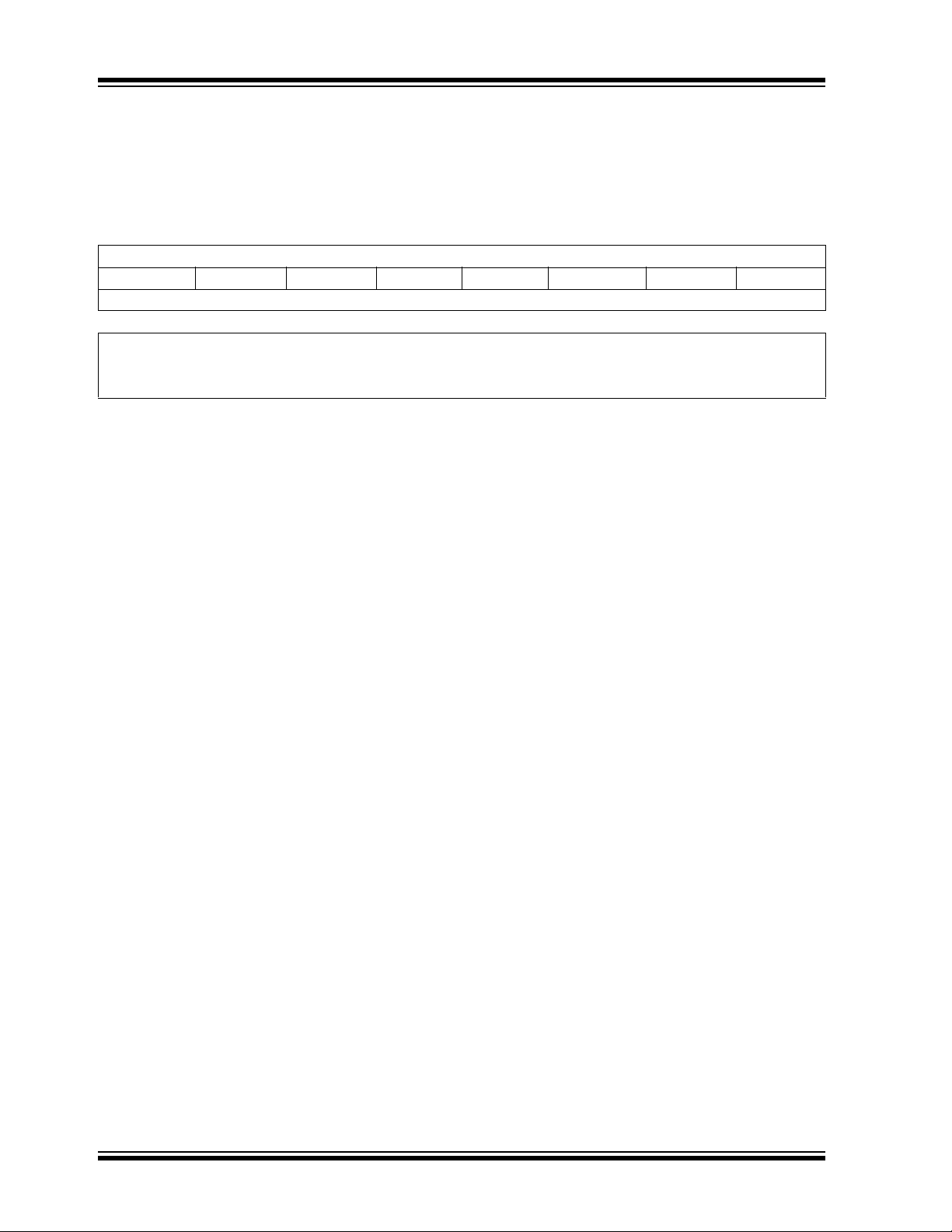
Page 2

MCP23008/MCP23S08
SDA
SCL
NC
INT
RESET
A1
GP4
VDD
GP7
GP6
GP5
GP3
GP2
1
2
3
4
5
6
7
18
17
16
15
14
13
12
PDIP/SOIC
8
9
11
10
GP1
GP0
A0
A2
VSS
MCP23008
MCP23008
MCP23008
13
12
1
2
3
4
5
6
7
8
9
20
19
18
17
16
15
14
11
10
GP3
V
DD
GP7
GP6
GP5
GP2
GP1
GP0
N/C
GP4
SDA
SCL
V
SS
A0
N/C
A1
RESET
A2
NC
INT
SSOP
MCP23008
20
19
18
17
16
6
7
8
9
10
15
14
13
12
11
1
2
3
4
5
QFN
SCL
SDA
VSS
A0
N/C
A1
RESET
A2
NC
INT
GP3
VDD
GP7
GP6
GP5
GP2
GP1
GP0
N/C
GP4
Package Types
DS21919E-page 2 © 2007 Microchip Technology Inc.
Page 3

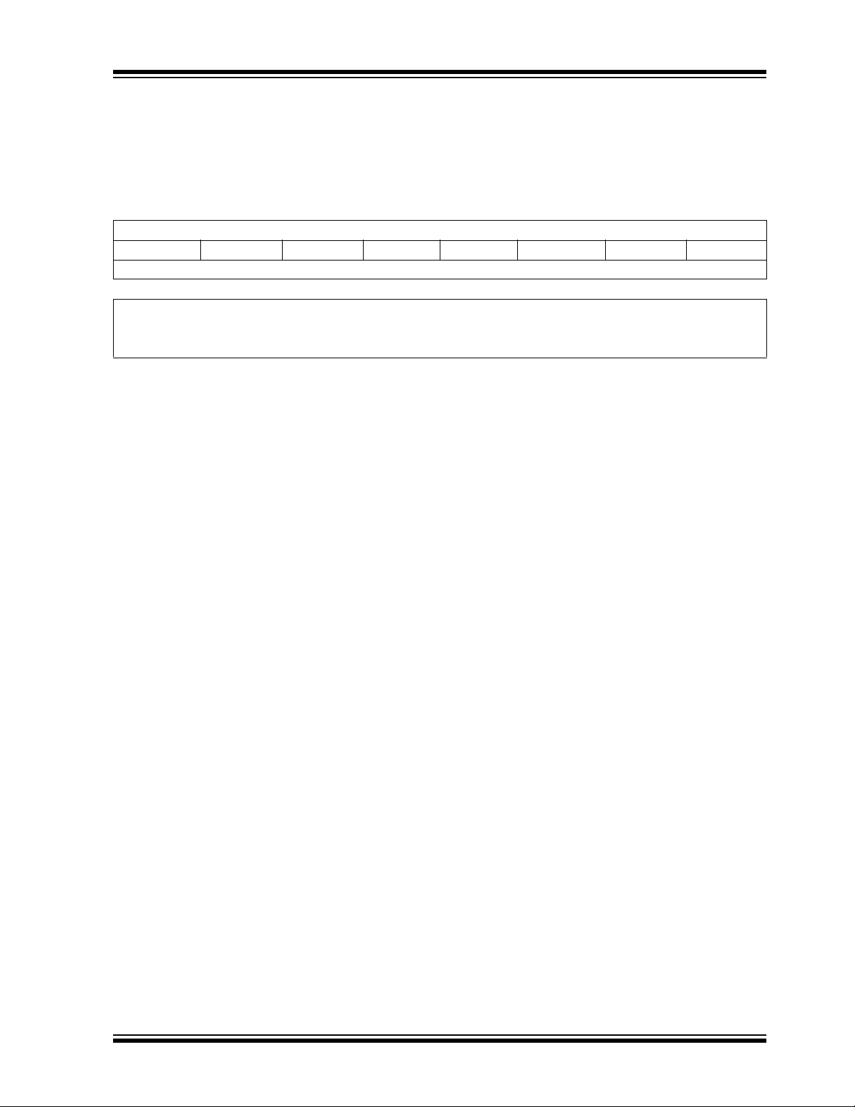
Package Types: (Continued)
SI
SCK
CS
INT
RESET
A1
GP4
VDD
GP7
GP6
GP5
GP3
GP2
1
2
3
4
5
6
7
18
17
16
15
14
13
12
PDIP/SOIC
8
9
11
10
GP1
GP0
A0
SO
V
SS
MCP23S08
MCP23S08
MCP23S08
13
12
1
2
3
4
5
6
7
8
9
20
19
18
17
16
15
14
11
10
GP3
V
DD
GP7
GP6
GP5
GP2
GP1
GP0
N/C
GP4
SI
SCK
V
SS
A0
N/C
A1
RESET
SO
CS
INT
SSOP
QFN
MCP23S08
20
19
18
17
16
6
7
8
9
10
15
14
13
12
11
1
2
3
4
5
SCK
SI
V
SS
A0
N/C
A1
RESET
A2
CS
INT
GP3
VDD
GP7
GP6
GP5
GP2
GP1
GP0
N/C
GP4
MCP23008/MCP23S08
© 2007 Microchip Technology Inc. DS21919E-page 3
Page 4

MCP23008/MCP23S08
NOTES:
DS21919E-page 4 © 2007 Microchip Technology Inc.
Page 5
MCP23008/MCP23S08
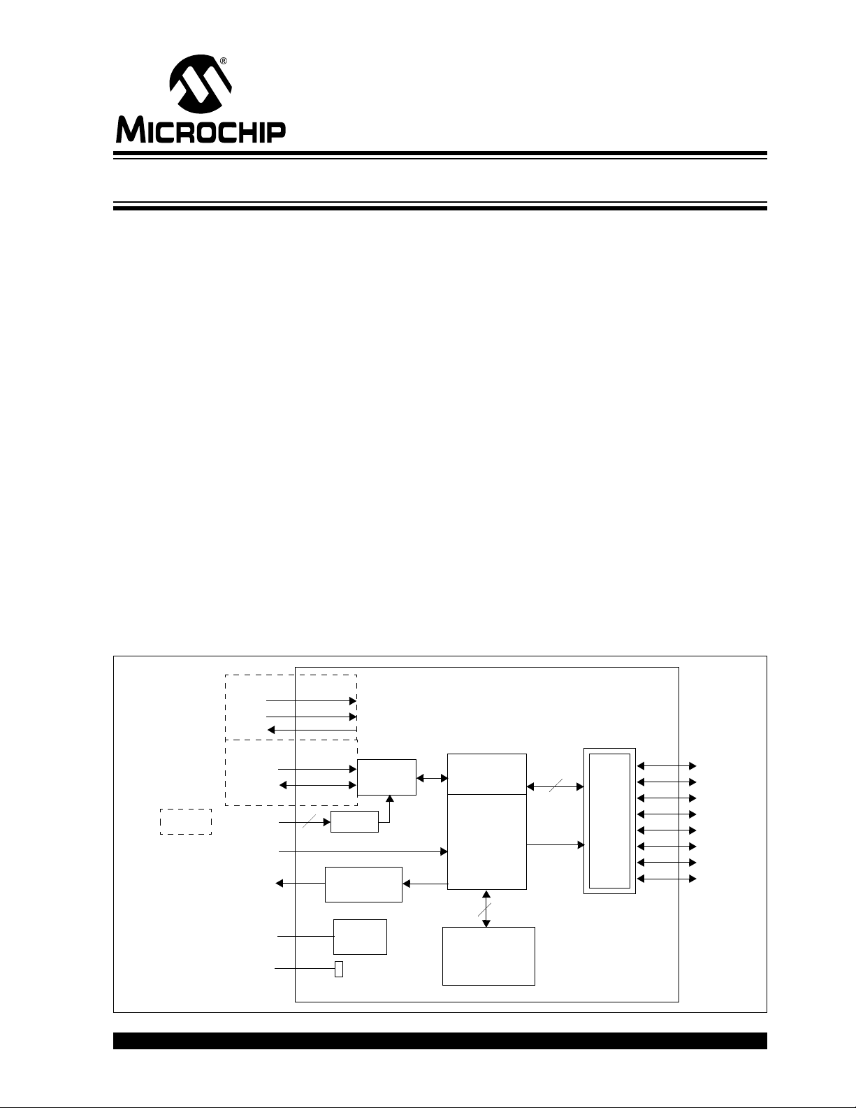
1.0 DEVICE OVERVIEW
The MCP23X08 device provides 8-bit, general
purpose, parallel I/O expansion for I2C bus or SPI
applications. The two devices differ in the number of
hardware address pins and the serial interface:
2
• MCP23008 – I
• MCP23S08 – SPI interface; two address pins
The MCP23X08 consists of multiple 8-bit configuration
registers for input, output and polarity selection. The
system master can enable the I/Os as either inputs or
outputs by writing the I/O configuration bits. The data
for each input or output is kept in the corresponding
Input or Output register. The polarity of the Input Port
register can be inverted with the Polarity Inversion
register. All registers can be read by the system master.
C interface; three address pins
The interrupt output can be configured to activate
under two conditions (mutually exclusive):
1. When any input state differs from its
corresponding input port register state, this is
used to indicate to the system master that an
input state has changed.
2. When an input state differs from a preconfigured
register value (DEFVAL register).
The Interrupt Capture register captures port values at
the time of the interrupt, thereby saving the condition
that caused the interrupt.
The Power-on Reset (POR) sets the registers to their
default values and initializes the device state machine.
The hardware address pins are used to determine the
device address.
1.1 Pin Descriptions
TABLE 1-1: PINOUT DESCRIPTION
Pin
Name
SCL/SCK 1 19 1 I Serial clock input.
SDA/SI 2 20 2 I/O Serial data I/O (MCP23008)/Serial data input (MCP23S08).
A2/SO 3 1 3 I/O Hardware address input (MCP23008)/
A1 4 2 4 I Hardware address input. Must be biased externally.
A0 5 3 5 I Hardware address input. Must be biased externally.
RESET
NC/CS
INT 8 7 8 O Interrupt output. Can be configured for active-high, active-low or
V
SS 9179PGround.
GP0 10 9 12 I/O Bidirectional I/O pin. Can be enabled for interrupt-on-change and/or
GP1 11 10 13 I/O Bidirectional I/O pin. Can be enabled for interrupt-on-change and/or
GP2 12 11 14 I/O Bidirectional I/O pin. Can be enabled for interrupt-on-change and/or
GP3 13 12 15 I/O Bidirectional I/O pin. Can be enabled for interrupt-on-change and/or
GP4 14 13 16 I/O Bidirectional I/O pin. Can be enabled for interrupt-on-change and/or
GP5 15 14 17 I/O Bidirectional I/O pin. Can be enabled for interrupt-on-change and/or
GP6 16 15 18 I/O Bidirectional I/O pin. Can be enabled for interrupt-on-change and/or
GP7 17 16 19 I/O Bidirectional I/O pin. Can be enabled for interrupt-on-change and/or
V
DD 18 18 20 P Power.
N/C — 6, 8 10, 11 — —
PDIP/
SOIC
6 4 6 I External reset input. Must be biased externally.
7 5 7 I No connect (MCP23008)/External chip select input (MCP23S08).
QFN SSOP
Pin
Typ e
Serial data output (MCP23S08).
A2 must be biased externally.
open-drain.
internal weak pull-up resistor.
internal weak pull-up resistor.
internal weak pull-up resistor.
internal weak pull-up resistor.
internal weak pull-up resistor.
internal weak pull-up resistor.
internal weak pull-up resistor.
internal weak pull-up resistor.
Function
© 2007 Microchip Technology Inc. DS21919E-page 5
Page 6

MCP23008/MCP23S08
1.2 Power-on Reset (POR)
The on-chip POR circuit holds the device in reset until
DD has reached a high enough voltage to deactivate
V
the POR circuit (i.e., release the device from Reset).
The maximum VDD rise time is specified in Section 2.0
“Electrical Characteristics”.
When the device exits the POR condition (releases
reset), device operating parameters (i.e., voltage,
temperature, serial bus frequency, etc.) must be met to
ensure proper operation.
1.3 Serial Interface
This block handles the functionality of the I2C
(MCP23008) or SPI (MCP23S08) interface protocol.
The MCP23X08 contains eleven registers that can be
addressed through the serial interface block (Table 1-2):
TABLE 1-2: REGISTER ADDRESSES
Address Access to:
00h IODIR
01h IPOL
02h GPINTEN
03h DEFVAL
04h INTCON
05h IOCON
06h GPPU
07h INTF
08h INTCAP (Read-only)
09h GPIO
0Ah OLAT
1.3.1 SEQUENTIAL OPERATION BIT
The Sequential Operation (SEQOP) bit (IOCON
register) controls the operation of the address pointer.
The address pointer can either be enabled (default) to
allow the address pointer to increment automatically
after each data transfer, or it can be disabled.
When operating in Sequential mode
(IOCON.SEQOP = 0), the address pointer automatically increments to the next address after each byte
is clocked.
When operating in Byte mode (IOCON.SEQOP = 1),
the MCP23X08 does not increment its address
counter after each byte during the data transfer. This
gives the ability to continually read the same address
by providing extra clocks (without additional control
bytes). This is useful for polling the GPIO register for
data changes.
1.3.2 I2C™ INTERFACE
1.3.2.1 I
The I2C Write operation includes the control byte and
register address sequence, as shown in the bottom of
Figure 1-1. This sequence is followed by eight bits of
data from the master and an Acknowledge (ACK) from
the MCP23008. The operation is ended with a STOP
or RESTART condition being generated by the master.
Data is written to the MCP23008 after every byte
transfer. If a STOP or RESTART condition is
generated during a data transfer, the data will not be
written to the MCP23008.
Byte writes and sequential writes are both supported
by the MCP23008. The MCP23008 increments its
address counter after each ACK during the data
transfer.
2
C Write Operation
1.3.2.2 I2C Read Operation
The I2C Read operation includes the control byte
sequence, as shown in the bottom of Figure 1-1. This
sequence is followed by another control byte (including the START condition and ACK) with the R/W bit
equal to a logic 1 (R/W = 1). The MCP23008 then
transmits the data contained in the addressed register.
The sequence is ended with the master generating a
STOP or RESTART condition.
1.3.2.3 I2C Sequential Write/Read
For sequential operations (Write or Read), instead of
transmitting a STOP or RESTART condition after the
data transfer, the master clocks the next byte pointed to
by the address pointer (see Section 1.3.1 “Sequential
Operation Bit” for details regarding sequential
operation control).
The sequence ends with the master sending a STOP or
RESTART condition.
The MCP23008 address pointer will roll over to
address zero after reaching the last register address.
Refer to Figure 1-1.
1.3.3 SPI INTERFACE
1.3.3.1 SPI Write Operation
The SPI Write operation is started by lowering CS. The
Write command (slave address with R/W bit cleared) is
then clocked into the device. The opcode is followed by
an address and at least one data byte.
1.3.3.2 SPI Read Operation
The SPI Read operation is started by lowering CS. The
SPI read command (slave address with R/W bit set) is
then clocked into the device. The opcode is followed by
an address, with at least one data byte being clocked
out of the device.
DS21919E-page 6 © 2007 Microchip Technology Inc.
Page 7
MCP23008/MCP23S08
S
P
SR
w
R
OP
ADDR
DOUT
DIN
- START
- RESTART
- STOP
- Write
- Read
- Device opcode
- Device address
- Data out from MCP23008
- Data into MCP23008
S
P
SR
W
R
OP ADDR
DIN DIN
....
S
P
W
R
OP
ADDR
D
OUT
DOUT
....
P
SR WOP
D
IN
DIN
....
P
P
SR R
DOUT DOUT
....
P
OP
D
OUT
DOUT
....
P
SR OP
DIN
....
P
OP
D
IN
S PWOP ADDR
DIN
DIN
....
Byte and Sequential Write
S
W
OP SR R
OP
D
OUT
DOUT
....
P
Byte and Sequential Read
S WOP ADDR
DIN
P
S
W
OP SR ROP
D
OUT
P
Byte
Sequential
Byte
Sequential
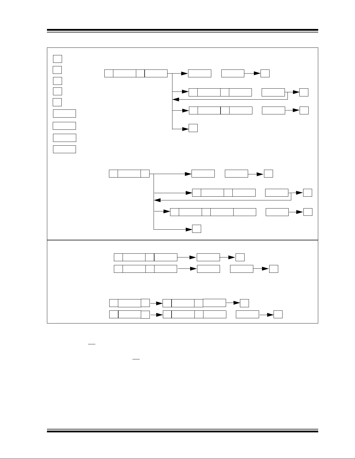
FIGURE 1-1: MCP23008 I2C™ DEVICE PROTOCOL
1.3.3.3 SPI Sequential Write/Read
For sequential operations, instead of deselecting the
device by raising CS, the master clocks the next byte
pointed to by the address pointer.
The sequence ends by the raising of CS
The MCP23S08 address pointer will roll over to
address zero after reaching the last register address.
© 2007 Microchip Technology Inc. DS21919E-page 7
.
1.4 Hardware Address Decoder
The hardware address pins are used to determine the
device address. To address a device, the corresponding address bits in the control byte must match the pin
state.
• MCP23008 has address pins A2, A1 and A0.
• MCP23S08 has address pins A1 and A0.
The pins must be biased externally.
Page 8
MCP23008/MCP23S08
S 0 1 0 0 A2A1A0R/WACK
Start
bit
Slave Address
R/W bit
ACK bit
Control Byte
R/W = 0 = write
R/W = 1 = read
01000A1A0R/W
Slave Address
R/W bit
Control Byte
R/W = 0 = write
R/W = 1 = read
CS
S0100A2A1A00ACKA7A6A5A4A3A2A1A0ACK
Device Opcode
Register Address
R/W = 0
The ACKs are provided by the MCP23008.
01000A1A0R/W A7A6A5A4A3A2A1A0
Device Opcode Register Address
CS
1.4.1 ADDRESSING I2C DEVICES
(MCP23008)
The MCP23008 is a slave I2C device that supports 7-bit
slave addressing, with the read/write bit filling out the
control byte. The slave address contains four fixed bits
and three user-defined hardware address bits (pins A2,
A1 and A0). Figure 1-2 shows the control byte format.
1.4.2 ADDRESSING SPI DEVICES
(MCP23S08)
The MCP23S08 is a slave SPI device. The slave
address contains five fixed bits and two user-defined
hardware address bits (pins A1 and A0), with the read/
write bit filling out the control byte. Figure 1-3 shows
the control byte format.
FIGURE 1-2: I2C™ CONTROL BYTE
FORMAT
FIGURE 1-3: SPI CONTROL BYTE
FORMAT
FIGURE 1-4: I
2
C™ ADDRESSING REGISTERS
FIGURE 1-5: SPI ADDRESSING REGISTERS
DS21919E-page 8 © 2007 Microchip Technology Inc.
Page 9
MCP23008/MCP23S08
1.5 GPIO Port
The GPIO module contains the data port (GPIO),
internal pull up resistors and the Output Latches
(OLAT).
1.6 Configuration and Control
Registers
The Configuration and Control blocks contain the
registers as shown in Table 1-3.
Reading the GPIO register reads the value on the port.
Reading the OLAT register only reads the OLAT, not
the actual value on the port.
Writing to the GPIO register actually causes a write to
the OLAT. Writing to the OLAT register forces the
associated output drivers to drive to the level in OLAT.
Pins configured as inputs turn off the associated output
driver and put it in high-impedance.
TABLE 1-3: CONFIGURATION AND CONTROL REGISTERS
Register
Name
IODIR 00 IO7 IO6 IO5 IO4 IO3 IO2 IO1 IO0 1111 1111
IPOL 01 IP7 IP6 IP5 IP4 IP3 IP2 IP1 IP0 0000 0000
GPINTEN 02 GPINT7 GPINT6 GPINT5 GPINT4 GPINT3 GPINT2 GPINT1 GPINT0 0000 0000
DEFVAL 03 DEF7 DEF6 DEF5 DEF4 DEF3 DEF2 DEF1 DEF0 0000 0000
INTCON 04 IOC7 IOC6 IOC5 IOC4 IOC3 IOC2 IOC1 IOC0 0000 0000
IOCON 05
GPPU 06 PU7 PU6 PU5 PU4 PU3 PU2 PU1 PU0 0000 0000
INTF 07 INT7 INT6 INT5 INT4 INT3 INT2 INT1 INTO 0000 0000
INTCAP 08 ICP7 ICP6 ICP5 ICP4 ICP3 ICP2 ICP1 ICP0 0000 0000
GPIO 09 GP7GP6GP5GP4GP3GP2GP1GP00000 0000
OLAT 0A OL7 OL6 OL5 OL4 OL3 OL2 OL1 OL0 0000 0000
Address
(hex)
bit 7 bit 6 bit 5 bit 4 bit 3 bit 2 bit 1 bit 0
— — SREAD DISSLW HAEN* ODR INTPOL — --00 000-
* Not used on the MCP23008.
POR/RST
value
© 2007 Microchip Technology Inc. DS21919E-page 9
Page 10
MCP23008/MCP23S08
1.6.1 I/O DIRECTION (IODIR) REGISTER
Controls the direction of the data I/O.
When a bit is set, the corresponding pin becomes an
input. When a bit is clear, the corresponding pin
becomes an output.
REGISTER 1-1: IODIR – I/O DIRECTION REGISTER (ADDR 0x00)
R/W-1 R/W-1 R/W-1 R/W-1 R/W-1 R/W-1 R/W-1 R/W-1
IO7 IO6 IO5 IO4 IO3 IO2 IO1 IO0
bit 7 bit 0
Legend:
R = Readable bit W = Writable bit U = Unimplemented bit, read as ‘0’
-n = Value at POR ‘1’ = Bit is set ‘0’ = Bit is cleared x = Bit is unknown
bit 7-0 IO7:IO0: These bits control the direction of data I/O <7:0>
1 = Pin is configured as an input.
0 = Pin is configured as an output.
DS21919E-page 10 © 2007 Microchip Technology Inc.
Page 11
MCP23008/MCP23S08
1.6.2 INPUT POLARITY (IPOL) REGISTER
The IPOL register allows the user to configure the
polarity on the corresponding GPIO port bits.
If a bit is set, the corresponding GPIO register bit will
reflect the inverted value on the pin.
REGISTER 1-2: IPOL – INPUT POLARITY PORT REGISTER (ADDR 0x01)
R/W-0 R/W-0 R/W-0 R/W-0 R/W-0 R/W-0 R/W-0 R/W-0
IP7 IP6 IP5 IP4 IP3 IP2 IP1 IP0
bit 7 bit 0
Legend:
R = Readable bit W = Writable bit U = Unimplemented bit, read as ‘0’
-n = Value at POR ‘1’ = Bit is set ‘0’ = Bit is cleared x = Bit is unknown
bit 7-0 IP7:IP0: These bits control the polarity inversion of the input pins <7:0>
1 = GPIO register bit will reflect the opposite logic state of the input pin.
0 = GPIO register bit will reflect the same logic state of the input pin.
© 2007 Microchip Technology Inc. DS21919E-page 11
Page 12
MCP23008/MCP23S08
1.6.3 INTERRUPT-ON-CHANGE
CONTROL (GPINTEN) REGISTER
The GPINTEN register controls the interrupt-onchange feature for each pin.
If a bit is set, the corresponding pin is enabled for
interrupt-on-change. The DEFVAL and INTCON
registers must also be configured if any pins are
enabled for interrupt-on-change.
REGISTER 1-3: GPINTEN – INTERRUPT-ON-CHANGE PINS (ADDR 0x02)
R/W-0 R/W-0 R/W-0 R/W-0 R/W-0 R/W-0 R/W-0 R/W-0
GPINT7 GPINT6 GPINT5 GPINT4 GPINT3 GPINT2 GPINT1 GPINT0
bit 7 bit 0
Legend:
R = Readable bit W = Writable bit U = Unimplemented bit, read as ‘0’
-n = Value at POR ‘1’ = Bit is set ‘0’ = Bit is cleared x = Bit is unknown
bit 7-0 GPINT7:GPINT0: General purpose I/O interrupt-on-change bits <7:0>
1 = Enable GPIO input pin for interrupt-on-change event.
0 = Disable GPIO input pin for interrupt-on-change event.
Refer to INTCON and GPINTEN.
DS21919E-page 12 © 2007 Microchip Technology Inc.
Page 13
MCP23008/MCP23S08
1.6.4 DEFAULT COMPARE (DEFVAL)
REGISTER FOR INTERRUPT-ONCHANGE
The default comparison value is configured in the
DEFVAL register. If enabled (via GPINTEN and
INTCON) to compare against the DEFVAL register, an
opposite value on the associated pin will cause an
interrupt to occur.
REGISTER 1-4: DEFVAL – DEFAULT VALUE REGISTER (ADDR 0x03)
R/W-0 R/W-0 R/W-0 R/W-0 R/W-0 R/W-0 R/W-0 R/W-0
DEF7 DEF6 DEF5 DEF4 DEF3 DEF2 DEF1 DEF0
bit 7 bit 0
Legend:
R = Readable bit W = Writable bit U = Unimplemented bit, read as ‘0’
-n = Value at POR ‘1’ = Bit is set ‘0’ = Bit is cleared x = Bit is unknown
bit 7-0 DEF7:DEF0: These bits set the compare value for pins configured for interrupt-on-change from
defaults <7:0>. Refer to INTCON.
If the associated pin level is the opposite from the register bit, an interrupt occurs.
Refer to INTCON and GPINTEN.
© 2007 Microchip Technology Inc. DS21919E-page 13
Page 14

MCP23008/MCP23S08
1.6.5 INTERRUPT CONTROL (INTCON)
REGISTER
The INTCON register controls how the associated pin
value is compared for the interrupt-on-change feature.
If a bit is set, the corresponding I/O pin is compared
against the associated bit in the DEFVAL register. If a
bit value is clear, the corresponding I/O pin is compared
against the previous value.
REGISTER 1-5: INTCON – INTERRUPT-ON-CHANGE CONTROL REGISTER (ADDR 0x04)
R/W-0 R/W-0 R/W-0 R/W-0 R/W-0 R/W-0 R/W-0 R/W-0
IOC7 IOC6 IOC5 IOC4 IOC3 IOC2 IOC1 IOC0
bit 7 bit 0
Legend:
R = Readable bit W = Writable bit U = Unimplemented bit, read as ‘0’
-n = Value at POR ‘1’ = Bit is set ‘0’ = Bit is cleared x = Bit is unknown
bit 7-0 IOC7:IOC0: These bits control how the associated pin value is compared for interrupt-on-change
<7:0>
1 = Controls how the associated pin value is compared for interrupt-on-change.
0 = Pin value is compared against the previous pin value.
Refer to INTCON and GPINTEN.
DS21919E-page 14 © 2007 Microchip Technology Inc.
Page 15

MCP23008/MCP23S08
1.6.6 CONFIGURATION (IOCON)
REGISTER
The IOCON register contains several bits for
configuring the device:
• The Sequential Operation (SEQOP) controls the
incrementing function of the address pointer. If the
address pointer is disabled, the address pointer
does not automatically increment after each byte
is clocked during a serial transfer. This feature is
useful when it is desired to continuously poll
(read) or modify (write) a register.
• The Slew Rate (DISSLW) bit controls the slew
rate function on the SDA pin. If enabled, the SDA
slew rate will be controlled when driving from a
high to a low.
• The Hardware Address Enable (HAEN) control bit
enables/disables the hardware address pins (A1,
A0) on the MCP23S08. This bit is not used on the
MCP23008. The address pins are always enabled
on the MCP23008.
• The Open-Drain (ODR) control bit enables/
disables the INT pin for open-drain configuration.
• The Interrupt Polarity (INTPOL) control bit sets
the polarity of the INT pin. This bit is functional
only when the ODR bit is cleared, configuring the
INT pin as active push-pull.
REGISTER 1-6: IOCON – I/O EXPANDER CONFIGURATION REGISTER (ADDR 0x05)
U-0 U-0 R/W-0 R/W-0 R/W-0 R/W-0 R/W-0 U-0
— —
bit 7 bit 0
Legend:
R = Readable bit W = Writable bit U = Unimplemented bit, read as ‘0’
-n = Value at POR ‘1’ = Bit is set ‘0’ = Bit is cleared x = Bit is unknown
SEQOP DISSLW HAEN ODR INTPOL
—
bit 7-6 Unimplemented: Read as ‘0’.
bit 5 SEQOP: Sequential Operation mode bit.
1 = Sequential operation disabled, address pointer does not increment.
0 = Sequential operation enabled, address pointer increments.
bit 4 DISSLW: Slew Rate control bit for SDA output.
1 = Slew rate disabled.
0 = Slew rate enabled.
bit 3 HAEN: Hardware Address Enable bit (MCP23S08 only).
Address pins are always enabled on MCP23008.
1 = Enables the MCP23S08 address pins.
0 = Disables the MCP23S08 address pins.
bit 2 ODR: This bit configures the INT pin as an open-drain output.
1 = Open-drain output (overrides the INTPOL bit).
0 = Active driver output (INTPOL bit sets the polarity).
bit 1 INTPOL: This bit sets the polarity of the INT output pin.
1 = Active-high.
0 = Active-low.
bit 0 Unimplemented: Read as ‘0’.
© 2007 Microchip Technology Inc. DS21919E-page 15
Page 16

MCP23008/MCP23S08
1.6.7 PULL-UP RESISTOR
CONFIGURATION (GPPU)
REGISTER
The GPPU register controls the pull-up resistors for the
port pins. If a bit is set and the corresponding pin is
configured as an input, the corresponding port pin is
internally pulled up with a 100 kΩ resistor.
REGISTER 1-7: GPPU – GPIO PULL-UP RESISTOR REGISTER (ADDR 0x06)
R/W-0 R/W-0 R/W-0 R/W-0 R/W-0 R/W-0 R/W-0 R/W-0
PU7 PU6 PU5 PU4 PU3 PU2 PU1 PU0
bit 7 bit 0
Legend:
R = Readable bit W = Writable bit U = Unimplemented bit, read as ‘0’
-n = Value at POR ‘1’ = Bit is set ‘0’ = Bit is cleared x = Bit is unknown
bit 7-0 PU7:PU0: These bits control the weak pull-up resistors on each pin (when configured as an input)
<7:0>.
1 = Pull-up enabled.
0 = Pull-up disabled.
DS21919E-page 16 © 2007 Microchip Technology Inc.
Page 17

MCP23008/MCP23S08
1.6.8 INTERRUPT FLAG (INTF)
REGISTER
The INTF register reflects the interrupt condition on the
port pins of any pin that is enabled for interrupts via the
GPINTEN register. A ‘set’ bit indicates that the
associated pin caused the interrupt.
This register is ‘read-only’. Writes to this register will be
ignored.
Note: INTF will always reflect the pin(s) that
have an interrupt condition. For example,
one pin causes an interrupt to occur and is
captured in INTCAP and INF. If before
clearing the interrupt another pin changes,
which would normally cause an interrupt, it
will be reflected in INTF, but not INTCAP.
REGISTER 1-8: INTF – INTERRUPT FLAG REGISTER (ADDR 0x07)
R-0 R-0 R-0 R-0 R-0 R-0 R-0 R-0
INT7 INT6 INT5 INT4 INT3 INT2 INT1 INT0
bit 7 bit 0
Legend:
R = Readable bit W = Writable bit U = Unimplemented bit, read as ‘0’
-n = Value at POR ‘1’ = Bit is set ‘0’ = Bit is cleared x = Bit is unknown
bit 7-0 INT7:INT0: These bits reflect the interrupt condition on the port. Will reflect the change only if interrupts
are enabled (GPINTEN) <7:0>.
1 = Pin caused interrupt.
0 = Interrupt not pending.
© 2007 Microchip Technology Inc. DS21919E-page 17
Page 18

MCP23008/MCP23S08
1.6.9 INTERRUPT CAPTURE (INTCAP)
REGISTER
The INTCAP register captures the GPIO port value at
the time the interrupt occurred. The register is ‘readonly’ and is updated only when an interrupt occurs. The
register will remain unchanged until the interrupt is
cleared via a read of INTCAP or GPIO.
REGISTER 1-9: INTCAP – INTERRUPT CAPTURED VALUE FOR PORT REGISTER (ADDR 0x08)
R-x R-x R-x R-x R-x R-x R-x R-x
ICP7 ICP6 ICP5 ICP4 ICP3 ICP2 ICP1 ICP0
bit 7 bit 0
Legend:
R = Readable bit W = Writable bit U = Unimplemented bit, read as ‘0’
-n = Value at POR ‘1’ = Bit is set ‘0’ = Bit is cleared x = Bit is unknown
bit 7-0 ICP7:ICP0: These bits reflect the logic level on the port pins at the time of interrupt due to pin change
<7:0>
1 = Logic-high.
0 = Logic-low.
DS21919E-page 18 © 2007 Microchip Technology Inc.
Page 19

MCP23008/MCP23S08
1.6.10 PORT (GPIO) REGISTER
The GPIO register reflects the value on the port.
Reading from this register reads the port. Writing to this
register modifies the Output Latch (OLAT) register.
REGISTER 1-10: GPIO – GENERAL PURPOSE I/O PORT REGISTER (ADDR 0x09)
R/W-0 R/W-0 R/W-0 R/W-0 R/W-0 R/W-0 R/W-0 R/W-0
GP7 GP6 GP5 GP4 GP3 GP2 GP1 GP0
bit 7 bit 0
Legend:
R = Readable bit W = Writable bit U = Unimplemented bit, read as ‘0’
-n = Value at POR ‘1’ = Bit is set ‘0’ = Bit is cleared x = Bit is unknown
bit 7-0 GP7:GP0: These bits reflect the logic level on the pins <7:0>
1 = Logic-high.
0 = Logic-low.
© 2007 Microchip Technology Inc. DS21919E-page 19
Page 20

MCP23008/MCP23S08
1.6.11 OUTPUT LATCH REGISTER (OLAT)
The OLAT register provides access to the output
latches. A read from this register results in a read of the
OLAT and not the port itself. A write to this register
modifies the output latches that modify the pins
configured as outputs.
REGISTER 1-11: OLAT – OUTPUT LATCH REGISTER 0 (ADDR 0x0A)
R/W-0 R/W-0 R/W-0 R/W-0 R/W-0 R/W-0 R/W-0 R/W-0
OL7 OL6 OL5 OL4 OL3 OL2 OL1 OL0
bit 7 bit 0
Legend:
R = Readable bit W = Writable bit U = Unimplemented bit, read as ‘0’
-n = Value at POR ‘1’ = Bit is set ‘0’ = Bit is cleared x = Bit is unknown
bit 7-0 OL7:OL0: These bits reflect the logic level on the output latch <7:0>
1 = Logic-high.
0 = Logic-low.
DS21919E-page 20 © 2007 Microchip Technology Inc.
Page 21

MCP23008/MCP23S08
GPx
INT ACTIVE ACTIVE
Port value
is captured
into INTCAP
Read GPIU
or INTCAP
Port value
is captured
into INTCAP
INT
Port value
is captured
into INTCAP
Read GPIU
or INTCAP
DEFVAL
X X X X X 0 X X
GP2
76543210GP:
ACTIVE
ACTIVE
(INT clears only if interrupt
condition does not exist.)
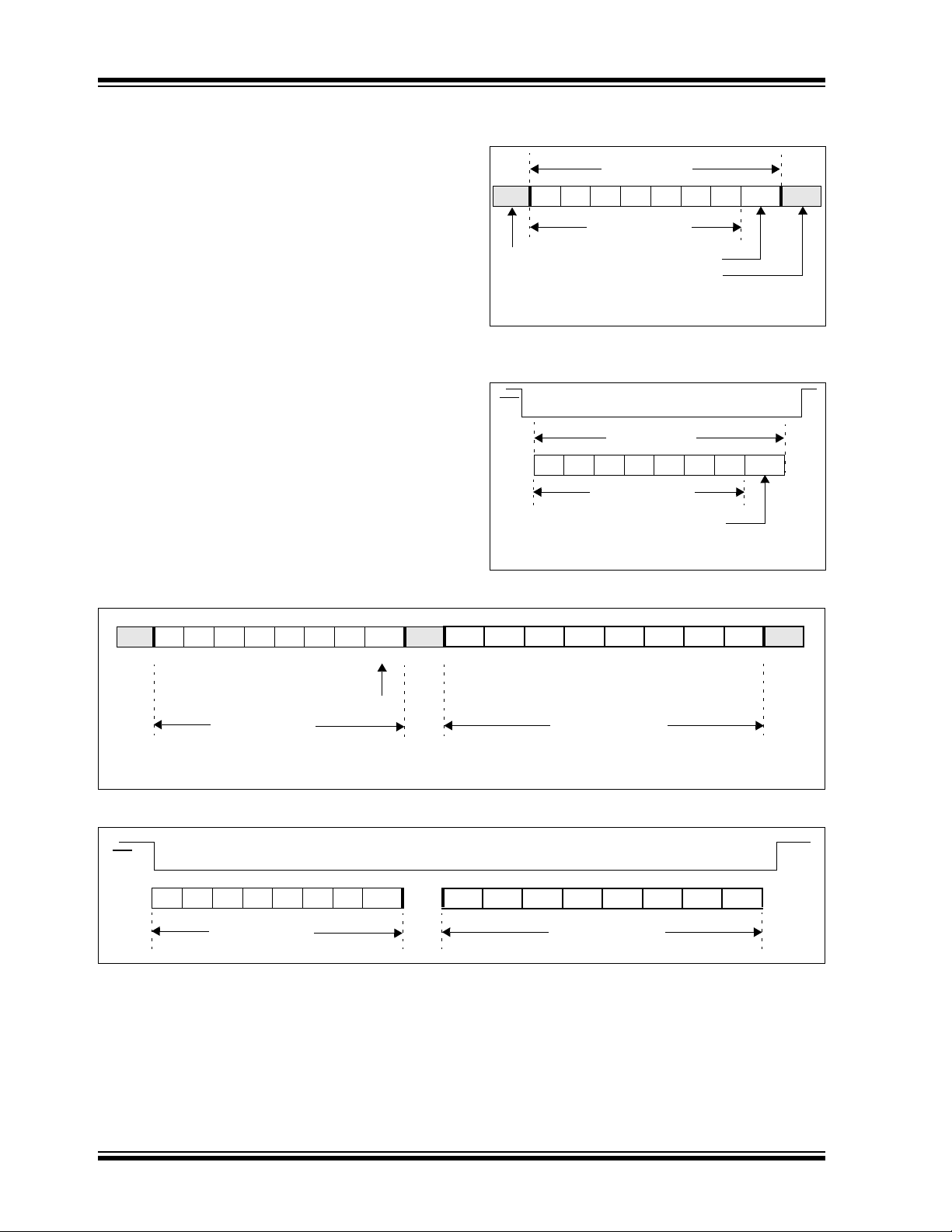
1.7 Interrupt Logic
The interrupt output pin will activate if an internal
interrupt occurs. The interrupt block is configured by
the following registers:
• GPINTEN – enables the individual inputs
• DEFVAL – holds the values that are compared
against the associated input port values
• INTCON – controls if the input values are
compared against DEFVAL or the previous values
on the port
• IOCON (ODR and INPOL) – configures the INT
pin as push-pull, open-drain and active-level
Only pins configured as inputs can cause interrupts.
Pins configured as outputs have no affect on INT.
Interrupt activity on the port will cause the port value to
be captured and copied into INTCAP. The interrupt will
remain active until the INTCAP or GPIO register is
read. Writing to these registers will not affect the
interrupt.
The first interrupt event will cause the port contents to
be copied into the INTCAP register. Subsequent
interrupt conditions on the port will not cause an
interrupt to occur as long as the interrupt is not cleared
by a read of INTCAP or GPIO.
FIGURE 1-6: INTERRUPT-ON-PIN-
CHANGE
FIGURE 1-7: INTERRUPT-ON-CHANGE
FROM REGISTER
DEFAULT
1.7.1 INTERRUPT CONDITIONS
There are two possible configurations to cause
interrupts (configured via INTCON):
1. Pins configured for interrupt-on-pin-change
will cause an interrupt to occur if a pin changes
to the opposite state. The default state is reset
after an interrupt occurs. For example, an
interrupt occurs by an input changing from 1 to
0. The new initial state for the pin is a logic 0.
2. Pins configured for interrupt-on-change from
register value will cause an interrupt to occur if
the corresponding input pin differs from the
register bit. The interrupt condition will remain as
long as the condition exists, regardless if the
INTAP or GPIO is read.
See Figure 1-6 and Figure 1-7 for more information on
interrupt operations.
© 2007 Microchip Technology Inc. DS21919E-page 21
Page 22

MCP23008/MCP23S08
NOTES:
DS21919E-page 22 © 2007 Microchip Technology Inc.
Page 23

MCP23008/MCP23S08
2.0 ELECTRICAL CHARACTERISTICS
Absolute Maximum Ratings †
Ambient temperature under bias.............................................................................................................-40°C to +125°C
Storage temperature .............................................................................................................................. -65°C to +150°C
Voltage on V
Voltage on all other pins with respect to V
Total power dissipation (Note) .............................................................................................................................700 mW
Maximum current out of V
Maximum current into V
Input clamp current, I
Output clamp current, I
Maximum output current sunk by any output pin ....................................................................................................25 mA
Maximum output current sourced by any output pin ...............................................................................................25 mA
Note: Power dissipation is calculated as follows:
†
NOTICE: Stresses above those listed under “Absolute Maximum Ratings” may cause permanent damage to the
device. This is a stress rating only and functional operation of the device at those or any other conditions above those
indicated in the operation listings of this specification is not implied. Exposure to maximum rating conditions for
extended periods may affect device reliability.
DD with respect to VSS ......................................................................................................... -0.3V to +5.5V
SS (except VDD)............................................................. -0.6V to (VDD + 0.6V)
SS pin ...........................................................................................................................150 mA
DD pin ..............................................................................................................................125 mA
IK (VI < 0 or VI > VDD)...................................................................................................................... ±20 mA
OK (VO < 0 or VO > VDD) .............................................................................................................. ±20 mA
DIS = VDD x {IDD - ∑ IOH} + ∑ {(VDD-VOH) x IOH} + ∑(VOL x IOL)
P
© 2007 Microchip Technology Inc. DS21919E-page 23
Page 24

MCP23008/MCP23S08
2.1 DC Characteristics
Operating Conditions (unless otherwise indicated):
DC Characteristics
1.8V ≤ VDD ≤ 5.5V at -40°C ≤ TA ≤ +85°C (I-Temp)
4.5V ≤ VDD ≤ 5.5V at -40°C ≤ TA ≤ +125°C (E-Temp) (Note 1)
Param
No.
D001 Supply Voltage V
D002 V
Characteristic Sym Min Typ Max Units Conditions
DD 1.8 — 5.5 V
DD Start Voltage to
VPOR —VSS —V
Ensure Power-on
Reset
D003 V
DD Rise Rate to
Ensure Power-on
SVDD 0.05 — — V/ms Design guidance only.
Not tested.
Reset
D004 Supply Current I
D005 Standby current I
DD — — 1 mA SCL/SCK = 1 MHz
DDS ——1µA
— — 2 µA 4.5V - 5.5V @ +125°C
(Note 1)
Input Low-Voltage
D030 A0, A1 (TTL buffer) V
D031 CS
, GPIO, SCL/SCK,
IL VSS —0.15VDD V
V
SS —0.2VDD V
SDA, A2, RESET
(Schmitt Trigger)
Input High-Voltage
D040 A0, A1
VIH 0.25 VDD + 0.8 — VDD V
(TTL buffer)
D041 CS
, GPIO, SCL/SCK,
0.8 V
DD —VDD V For entire VDD range.
SDA, A2, RESET
(Schmitt Trigger)
Input Leakage Current
D060 I/O port pins IIL ——±1µAVSS ≤ VPIN ≤ VDD
Output Leakage Current
D065 I/O port pins I
D070 GPIO weak pull-up
current
LO ——±1µAVSS ≤ VPIN ≤ VDD
IPU 40 75 115 µA VDD = 5V, GP Pins = VSS
–40°C ≤ TA ≤ +85°C
Output Low-Voltage
D080 GPIO V
INT — — 0.6 V I
SO, SDA — — 0.6 V I
SDA — — 0.8 V I
OL ——0.6VIOL = 8.5 mA, VDD = 4.5V
OL = 1.6 mA, VDD = 4.5V
OL = 3.0 mA, VDD = 1.8V
OL = 3.0 mA, VDD = 4.5V
Output High-Voltage
D090 GPIO, INT, SO V
OH VDD – 0.7 — — V IOH = -3.0 mA, VDD = 4.5V
V
DD – 0.7 — — IOH = -400 µA, VDD = 1.8V
Capacitive Loading Specs on Output Pins
D101 GPIO, SO, INT C
D102 SDA C
IO ——50pF
B — — 400 pF
Note 1: This parameter is characterized, not 100% tested.
DS21919E-page 24 © 2007 Microchip Technology Inc.
Page 25

MCP23008/MCP23S08
135 pF
1kΩ
VDD
SCL and
SDA pin
MCP23008
50 pF
Pin
VDD
RESET
Internal
RESET
34
Output pin
32
30
FIGURE 2-1: LOAD CONDITIONS FOR DEVICE TIMING SPECIFICATIONS
FIGURE 2-2: RESET AND DEVICE RESET TIMER TIMING
© 2007 Microchip Technology Inc. DS21919E-page 25
Page 26

MCP23008/MCP23S08
91
93
SCL
SDA
START
Condition
STOP
Condition
90
92
90
91 92
100
101
103
106
107
109
109
110
102
SCL
SDA
In
SDA
Out
TABLE 2-1: DEVICE RESET SPECIFICATIONS
Operating Conditions (unless otherwise indicated):
AC Characteristics
1.8V ≤ VDD ≤ 5.5V at -40°C ≤ TA ≤ +85°C (I-Temp)
4.5V ≤ VDD ≤ 5.5V at -40°C ≤ TA ≤ +125°C (E-Temp) (Note 1)
Param
No.
30 RESET
32 Device Active After
34 Output High-Impedance
Note 1: This parameter is characterized, not 100% tested.
FIGURE 2-3: I
Characteristic Sym Min Typ
Pulse Width
(Low)
RESET
From RESET
high
Low
2
C™ BUS START/STOP BITS TIMING
TRSTL1 — — µs
THLD —0—µsVDD = 5.0V
TIOZ —— 1 µs
(1)
Max Units Conditions
FIGURE 2-4: I
DS21919E-page 26 © 2007 Microchip Technology Inc.
2
C™ BUS DATA TIMING
Page 27
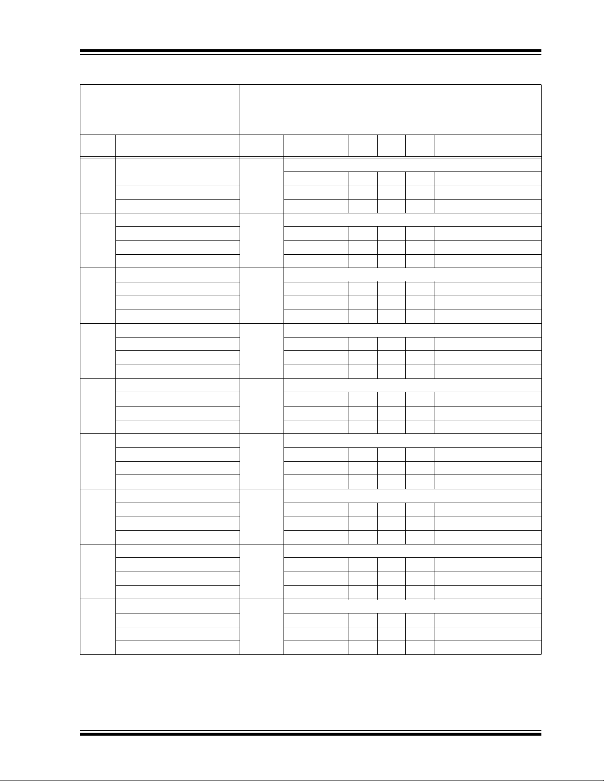
TABLE 2-2: I2C™ BUS DATA REQUIREMENTS
Operating Conditions (unless otherwise indicated):
I2C™ AC Characteristics
1.8V ≤ V
4.5V ≤ V
RPU (SCL, SDA) = 1 kΩ, CL (SCL, SDA) = 135 pF
Param
Characteristic Sym Min Typ Max Units Conditions
No.
100 Clock High Time: THIGH
100 kHz mode 4.0 — — µs 1.8V – 5.5V (I-Temp)
400 kHz mode 0.6 — — µs 2.7V – 5.5V (I-Temp)
1.7 MHz mode 0.12 — — µs 4.5V – 5.5V (E-Temp)
101 Clock Low Time: T
100 kHz mode 4.7 — — µs 1.8V – 5.5V (I-Temp)
400 kHz mode 1.3 — — µs 2.7V – 5.5V (I-Temp)
1.7 MHz mode 0.32 — — µs 4.5V – 5.5V (E-Temp)
102 SDA and SCL Rise Time: T
100 kHz mode — — 1000 ns 1.8V – 5.5V (I-Temp)
(Note 1)
400 kHz mode 20 + 0.1 C
1.7 MHz mode 20 — 160 ns 4.5V – 5.5V (E-Temp)
103 SDA and SCL Fall Time: T
100 kHz mode — — 300 ns 1.8V – 5.5V (I-Temp)
(Note 1)
400 kHz mode 20 + 0.1 C
1.7 MHz mode 20 — 80 ns 4.5V – 5.5V (E-Temp)
90 START Condition Setup Time: T
100 kHz mode 4.7 — — µs 1.8V – 5.5V (I-Temp)
400 kHz mode 0.6 — — µs 2.7V – 5.5V (I-Temp)
1.7 MHz mode 0.16 — — µs 4.5V – 5.5V (E-Temp)
91 START Condition Hold Time: T
100 kHz mode 4.0 — — µs 1.8V – 5.5V (I-Temp)
400 kHz mode 0.6 — — µs 2.7V – 5.5V (I-Temp)
1.7 MHz mode 0.16 — — µs 4.5V – 5.5V (E-Temp)
106 Data Input Hold Time: T
100 kHz mode 0 — 3.45 µs 1.8V – 5.5V (I-Temp)
400 kHz mode 0 — 0.9 µs 2.7V – 5.5V (I-Temp)
1.7 MHz mode 0 — 0.15 µs 4.5V – 5.5V (E-Temp)
107 Data Input Setup Time: T
100 kHz mode 250 — — ns 1.8V – 5.5V (I-Temp)
400 kHz mode 100 — — ns 2.7V – 5.5V (I-Temp)
1.7 MHz mode 0.01 — — µs 4.5V – 5.5V (E-Temp)
92 STOP Condition Setup Time: T
100 kHz mode 4.0 — — µs 1.8V – 5.5V (I-Temp)
400 kHz mode 0.6 — — µs 2.7V – 5.5V (I-Temp)
1.7 MHz mode 0.16 — — µs 4.5V – 5.5V (E-Temp)
Note 1: This parameter is characterized, not 100% tested.
2: C
B is specified to be from 10 to 400 pF.
DD ≤ 5.5V at -40°C ≤ TA ≤ +85°C (I-Temp)
DD ≤ 5.5V at -40°C ≤ TA ≤ +125°C (E-Temp) (Note 1)
LOW
R
F
SU:STA
HD:STA
HD:DAT
SU:DAT
SU:STO
MCP23008/MCP23S08
(2)
B
— 300 ns 2.7V – 5.5V (I-Temp)
(2)
B
— 300 ns 2.7V – 5.5V (I-Temp)
© 2007 Microchip Technology Inc. DS21919E-page 27
Page 28

MCP23008/MCP23S08
CS
SCK
SI
SO
1
5
4
7
6
3
10
2
LSb in
MSb in
high-impedance
11
Mode 1,1
Mode 0,0
TABLE 2-2: I2C™ BUS DATA REQUIREMENTS (CONTINUED)
Operating Conditions (unless otherwise indicated):
I2C™ AC Characteristics
1.8V ≤ V
4.5V ≤ V
RPU (SCL, SDA) = 1 kΩ, CL (SCL, SDA) = 135 pF
Param
Characteristic Sym Min Typ Max Units Conditions
No.
109 Output Valid From Clock: TAA
100 kHz mode — — 3.45 µs 1.8V – 5.5V (I-Temp)
400 kHz mode — — 0.9 µs 2.7V – 5.5V (I-Temp)
1.7 MHz mode — — 0.18 µs 4.5V – 5.5V (E-Temp)
110 Bus Free Time: T
100 kHz mode 4.7 — — µs 1.8V – 5.5V (I-Temp)
400 kHz mode 1.3 — — µs 2.7V – 5.5V (I-Temp)
1.7 MHz mode N/A — N/A µs 4.5V – 5.5V (E-Temp)
Bus Capacitive Loading: C
100 kHz and 400 kHz — — 400 pF (Note 1)
1.7 MHz — — 100 pF (Note 1)
Input Filter Spike
Suppression: (SDA and SCL)
100 kHz and 400 kHz — — 50 ns
1.7 MHz — — 10 ns Spike suppression off
Note 1: This parameter is characterized, not 100% tested.
B is specified to be from 10 to 400 pF.
2: C
DD ≤ 5.5V at -40°C ≤ TA ≤ +85°C (I-Temp)
DD ≤ 5.5V at -40°C ≤ TA ≤ +125°C (E-Temp) (Note 1)
BUF
B
T
SP
FIGURE 2-5: SPI INPUT TIMING
DS21919E-page 28 © 2007 Microchip Technology Inc.
Page 29

MCP23008/MCP23S08
CS
SCK
SO
8
13
MSb out
LSb out
2
14
don’t care
SI
Mode 1,1
Mode 0,0
9
12
FIGURE 2-6: SPI OUTPUT TIMING
TABLE 2-3: SPI INTERFACE AC CHARACTERISTICS
Operating Conditions (unless otherwise indicated):
SPI Interface AC Characteristics
1.8V ≤ VDD ≤ 5.5V at -40°C ≤ TA ≤ +85°C (I-Temp)
4.5V ≤ VDD ≤ 5.5V at -40°C ≤ TA ≤ +125°C (E-Temp) (Note 1)
Param
No.
Characteristic Sym Min Typ Max Units Conditions
Clock Frequency FCLK — — 5 MHz 1.8V – 5.5V (I-Temp)
— — 10 MHz 2.7V – 5.5V (I-Temp)
— — 10 MHz 4.5V – 5.5V (E-Temp)
1CS
2CS
Setup Time TCSS 50 — — ns
Hold Time TCSH 100 — — ns 1.8V – 5.5V (I-Temp)
50 — — ns 2.7V – 5.5V (I-Temp)
50 — — ns 4.5V – 5.5V (E-Temp)
3CS
Disable Time TCSD 100 — — ns 1.8V – 5.5V (I-Temp)
50 — — ns 2.7V – 5.5V (I-Temp)
50 — — ns 4.5V – 5.5V (E-Temp)
4 Data Setup Time T
SU 20 — — ns 1.8V – 5.5V (I-Temp)
10 — — ns 2.7V – 5.5V (I-Temp)
10 — — ns 4.5V – 5.5V (E-Temp)
5 Data Hold Time T
HD 20 — — ns 1.8V – 5.5V (I-Temp)
10 — — ns 2.7V – 5.5V (I-Temp)
10 — — ns 4.5V – 5.5V (E-Temp)
6 CLK Rise Time T
7 CLK Fall Time T
8 Clock High Time T
R —— 2 µsNote 1
F —— 2 µsNote 1
HI 90 — — ns 1.8V – 5.5V (I-Temp)
45 — — ns 2.7V – 5.5V (I-Temp)
45 — — ns 4.5V – 5.5V (E-Temp)
Note 1: This parameter is characterized, not 100% tested.
V = 90 ns (max) when address pointer rolls over from address 0x0A to 0x00.
2: T
© 2007 Microchip Technology Inc. DS21919E-page 29
Page 30

MCP23008/MCP23S08
50
SCL/SCK
SDA/SI
In
GPn
Pin
D0
D1
LSb of data byte zero
during a write or read
INT
Pin
INT pin active
51
command, depending
on parameter.
Output
GPn
Pin
Input
inactive
53
52
Register
Loaded
TABLE 2-3: SPI INTERFACE AC CHARACTERISTICS (CONTINUED)
Operating Conditions (unless otherwise indicated):
SPI Interface AC Characteristics
1.8V ≤ VDD ≤ 5.5V at -40°C ≤ TA ≤ +85°C (I-Temp)
4.5V ≤ VDD ≤ 5.5V at -40°C ≤ TA ≤ +125°C (E-Temp) (Note 1)
Param
No.
Characteristic Sym Min Typ Max Units Conditions
9 Clock Low Time TLO 90 — — ns 1.8V – 5.5V (I-Temp)
45 — — ns 2.7V – 5.5V (I-Temp)
45 — — ns 4.5V – 5.5V (E-Temp)
10 Clock Delay Time T
11 Clock Enable Time T
(2)
12
Output Valid from Clock Low TV — — 90 ns 1.8V – 5.5V (I-Temp)
CLD 50 — — ns
CLE 50 — — ns
— — 45 ns 2.7V – 5.5V (I-Temp)
— — 45 ns 4.5V – 5.5V (E-Temp)
13 Output Hold Time T
14 Output Disable Time T
HO 0——ns
DIS ——100ns
Note 1: This parameter is characterized, not 100% tested.
2: TV = 90 ns (max) when address pointer rolls over from address 0x0A to 0x00.
FIGURE 2-7: GPIO AND INT TIMING
DS21919E-page 30 © 2007 Microchip Technology Inc.
Page 31

TABLE 2-4: GP AND INT PINS
AC Characteristics
MCP23008/MCP23S08
Operating Conditions (unless otherwise indicated):
1.8V ≤ VDD ≤ 5.5V at -40°C ≤ TA ≤ +85°C (I-Temp)
4.5V ≤ V
DD ≤ 5.5V at -40°C ≤ TA ≤ +125°C (E-Temp) (Note 1)
Param
No.
50 Serial data to output valid T
51 Interrupt pin disable time T
52 GP input change to register
53 IOC event to INT active TGPINT ——600ns
Note 1: This parameter is characterized, not 100% tested
Characteristic Sym Min Typ Max Units Conditions
GPOV ——500ns
INTD ——600ns
TGPIV ——450ns
valid
Glitch Filter on GP Pins TGLITCH ——150ns
© 2007 Microchip Technology Inc. DS21919E-page 31
Page 32

MCP23008/MCP23S08
NOTES:
DS21919E-page 32 © 2007 Microchip Technology Inc.
Page 33

3.0 PACKAGING INFORMATION
18-Lead PDIP (300 mil)
18-Lead SOIC (300 mil)
20-Lead SSOP
XXXXXXXXXXXX
XXXXXXXXXXXX
XXXXXXXXXXXX
YYWWNNN
XXXXXXXXXXXXXXXXX
XXXXXXXXXXXXXXXXX
YYWWNNN
Example:
Example:
Example:
MCP23008
0634256
MCP23008-E/P^^
0634256
XXXXXXXXXXXX
XXXXXXXXXXXX
YYWWNNN
MCP23S08
XXXXXXXXXXXX
0634256
E/SO^^
E/SS^^
Legend: XX...X Customer-specific information
Y Year code (last digit of calendar year)
YY Year code (last 2 digits of calendar year)
WW Week code (week of January 1 is week ‘01’)
NNN Alphanumeric traceability code
Pb-free JEDEC designator for Matte Tin (Sn)
* This package is Pb-free. The Pb-free JEDEC designator ( )
can be found on the outer packaging for this package.
Note: In the event the full Microchip part number cannot be marked on one line, it will
be carried over to the next line, thus limiting the number of available
characters for customer-specific information.
3
e
3
e
20-Lead QFN
Example
XXXXX
XXXXXX
XXXXXX
YWWNNN
23S08
E/ML^^
0637
256
3
e
3.1 Package Marking Information
MCP23008/MCP23S08
3
e
3
3
e
e
© 2007 Microchip Technology Inc. DS21919E-page 33
Page 34

MCP23008/MCP23S08
18-Lead Plastic Dual In-Line (P) – 300 mil Body [PDIP]
Notes:
1. Pin 1 visual index feature may vary, but must be located within the hatched area.
2. § Significant Characteristic.
3. Dimensions D and E1 do not include mold flash or protrusions. Mold flash or protrusions shall not exceed .010" per side.
4. Dimensioning and tolerancing per ASME Y14.5M.
BSC: Basic Dimension. Theoretically exact value shown without tolerances.
Note: For the most current package drawings, please see the Microchip Packaging Specification located at
http://www.microchip.com/packaging
Units INCHES
Dimension Limits MIN NOM MAX
Number of Pins N 18
Pitch e .100 BS C
Top to Seating Plane A – – .210
Molded Package Thickness A2 .115 .130 .195
Base to Seating Plane A1 .015 – –
Shoulder to Shoulder Width E .300 .310 .325
Molded Package Width E1 .240 .250 .280
Overall Length D .880 .900 .920
Tip to Seating Plane L .115 .130 .150
Lead Thickness c .008 .010 .014
Upper Lead Width b1 .045 .060 .070
Lower Lead Width b .014 .018 .022
Overall Row Spacing § eB – – .430
NOTE 1
N
E1
D
1
2 3
A
A1
A2
L
E
eB
c
e
b1
b
Microchip Technology Drawing C04-007B
DS21919E-page 34 © 2007 Microchip Technology Inc.
Page 35

MCP23008/MCP23S08
18-Lead Plastic Small Outline (SO) – Wide, 7.50 mm Body [SOIC]
Notes:
1. Pin 1 visual index feature may vary, but must be located within the hatched area.
2. § Significant Characteristic.
3. Dimensions D and E1 do not include mold flash or protrusions. Mold flash or protrusions shall not exceed 0.15 mm per side.
4. Dimensioning and tolerancing per ASME Y14.5M.
BSC: Basic Dimension. Theoretically exact value shown without tolerances.
REF: Reference Dimension, usually without tolerance, for information purposes only.
Note: For the most current package drawings, please see the Microchip Packaging Specification located at
http://www.microchip.com/packaging
Units MILLIMETERS
Dimension Limits MIN NOM MAX
Number of Pins N 18
Pitch e 1.27 BSC
Overall Height A – – 2.65
Molded Package Thickness A2 2.05 – –
Standoff § A1 0.10 – 0.30
Overall Width E 10.30 BSC
Molded Package Width E1 7.50 BSC
Overall Length D 11.55 BSC
Chamfer (optional) h 0.25 – 0.75
Foot Length L 0.40 – 1.27
Footprint L1 1.40 REF
Foot Angle φ 0° – 8°
Lead Thickness c 0.20 – 0.33
Lead Width b 0.31 – 0.51
Mold Draft Angle Top α 5° – 15°
Mold Draft Angle Bottom β 5° – 15°
NOTE 1
D
N
E
E1
e
b
1
2 3
A
A1
A2
L
L1
h
h
c
β
φ
α
Microchip Technology Drawing C04-051B
© 2007 Microchip Technology Inc. DS21919E-page 35
Page 36

MCP23008/MCP23S08
20-Lead Plastic Quad Flat, No Lead Package (ML) – 4x4x0.9 mm Body [QFN]
Notes:
1. Pin 1 visual index feature may vary, but must be located within the hatched area.
2. Package is saw singulated.
3. Dimensioning and tolerancing per ASME Y14.5M.
BSC: Basic Dimension. Theoretically exact value shown without tolerances.
REF: Reference Dimension, usually without tolerance, for information purposes only.
Note: For the most current package drawings, please see the Microchip Packaging Specification located at
http://www.microchip.com/packaging
Units MILLIMETERS
Dimension Limits MIN NOM MAX
Number of Pins N 20
Pitch e 0.50 BSC
Overall Height A 0.80 0.90 1.00
Standoff A1 0.00 0.02 0.05
Contact Thickness A3 0.20 REF
Overall Width E 4.00 BSC
Exposed Pad Width E2 2.60 2.70 2.80
Overall Length D 4.00 BSC
Exposed Pad Length D2 2.60 2.70 2.80
Contact Width b 0.18 0.25 0.30
Contact Length L 0.30 0.40 0.50
Contact-to-Exposed Pad K 0.20 – –
D
EXPOSED
PAD
E
E2
2
1
N
TOP VIEW
NOTE 1
N
L
K
b
e
D2
2
1
A
A1
A3
BOTTOM VIEW
Microchip Technology Drawing C04-126B
DS21919E-page 36 © 2007 Microchip Technology Inc.
Page 37

MCP23008/MCP23S08
20-Lead Plastic Shrink Small Outline (SS) – 5.30 mm Body [SSOP]
Notes:
1. Pin 1 visual index feature may vary, but must be located within the hatched area.
2. Dimensions D and E1 do not include mold flash or protrusions. Mold flash or protrusions shall not exceed 0.20 mm per side.
3. Dimensioning and tolerancing per ASME Y14.5M.
BSC: Basic Dimension. Theoretically exact value shown without tolerances.
REF: Reference Dimension, usually without tolerance, for information purposes only.
Note: For the most current package drawings, please see the Microchip Packaging Specification located at
http://www.microchip.com/packaging
Units MILLIMETERS
Dimension Limits MIN NOM MAX
Number of Pins N 20
Pitch e 0.65 BSC
Overall Height A – – 2.00
Molded Package Thickness A2 1.65 1.75 1.85
Standoff A1 0.05 – –
Overall Width E 7.40 7.80 8.20
Molded Package Width E1 5.00 5.30 5.60
Overall Length D 6.90 7.20 7.50
Foot Length L 0.55 0.75 0. 95
Footprint L1 1.25 REF
Lead Thickness c 0.09 – 0.25
Foot Angle φ 0° 4° 8°
Lead Width b 0.22 – 0.38
φ
L
L1
A2
c
e
b
A1
A
12
NOTE 1
E1
E
D
N
Microchip Technology Drawing C04-072B
© 2007 Microchip Technology Inc. DS21919E-page 37
Page 38

MCP23008/MCP23S08
NOTES:
DS21919E-page 38 © 2007 Microchip Technology Inc.
Page 39

APPENDIX A: REVISION HISTORY
Revision E (August 2007)
1. Section 3.0 “Packaging Information”:
Updated package outline drawings.
Revision D (February 2007)
1. Changed Byte and Sequential Read in
Figure 1-1 from “R” to “W”.
2. Table 2-4, Param No. 51 and 53: Changed from
450 to 600 and 500 to 600, respecively.
3. Added disclaimer to package outline drawings.
4. Updated package outline drawings.
Revision C (October 2006)
1. Added 20-pin QFN package information
throughout document.
2. Added disclaimer to package outline drawings.
Revision B (February 2005)
MCP23008/MCP23S08
The following is the list of modifications:
1. Section 1.6 “Configuration and Control Reg-
isters”. Added Hardware Address Enable
(HAEN) bit to Table 1-3.
2. Section 1.6.6 “Configuration (IOCON) Regis-
ter”. Added Hardware Address Enable (HAEN)
bit to Register 1-6.
Revision A (December 2004)
• Original Release of this Document.
© 2007 Microchip Technology Inc. DS21919E-page 39
Page 40

MCP23008/MCP23S08
NOTES:
DS21919E-page 40 © 2007 Microchip Technology Inc.
Page 41

MCP23008/MCP23S08
Device MCP23008: 8-Bit I/O Expander w/ I2C™ Interface
MCP23008T: 8-Bit I/O Expander w/ I
2
C Interface
(Tape and Reel)
MCP23S08: 8-Bit I/O Expander w/ SPI Interface
MCP23S08T: 8-Bit I/O Expander w/ SPI Interface
(Tape and Reel)
Temperature
Range
E= -40°C to +125°C (Extended) *
* While these devices are only offered in the “E”
temperature range, the device will operate at different
voltages and temperatures as identified in the
Section 2.0 “Electrical Characteristics”.
Package ML = Plastic Quad Flat, No Lead Package
4x4x0.9 mm Body (QFN), 20-Lead
P = Plastic DIP (300 mil Body), 18-Lead
SO = Plastic SOIC (300 mil Body), 18-Lead
SS = SSOP, (209 mil Body, 5.30 mm), 20-Lead
PART NO. X /XX
PackageTemperature
Range
Device
Examples:
a) MCP23008-E/P: Extended Temp.,
18LD PDIP package.
b) MCP23008-E/SO: Extended Temp.,
18LD SOIC package.
c) MCP23008T-E/SO: Tape and Reel,
Extended Temp.,
18LD SOIC package.
d) MCP23008-E/SS: Extended Temp.,
20LD SSOP package.
e) MCP23008T-E/SS: Tape and Reel,
Extended Temp.,
20LD SSOP package.
f) MCP23008-E/ML: Extended Temp.,
20LD QFN package.
a) MCP23S08-E/P: Extended Temp.,
18LD PDIP package.
b) MCP23S08-E/SO: Extended Temp.,
18LD SOIC package.
c) MCP23S08T-E/SO: Tape and Reel,
Extended Temp.,
18LD SOIC package.
d) MCP23S08-E/SS: Extended Temp.,
20LD SSOP package.
e) MCP23S08T-E/SS: Tape and Reel,
Extended Temp.,
20LD SSOP package.
f) MCP23S08T-E/MF: Tape and Reel,
Extended Temp.,
20LD QFN package.
–
PRODUCT IDENTIFICATION SYSTEM
To order or obtain information, e.g., on pricing or delivery, refer to the factory or the listed sales office.
© 2007 Microchip Technology Inc. DS21919E-page 41
Page 42

MCP23008/MCP23S08
NOTES:
DS21919E-page 42 © 2007 Microchip Technology Inc.
Page 43

Note the following details of the code protection feature on Microchip devices:
• Microchip products meet the specification contained in their particular Microchip Data Sheet.
• Microchip believes that its family of products is one of the most secure families of its kind on the market today, when used in the
intended manner and under normal conditions.
• There are dishonest and possibly illegal methods used to breach the code protection feature. All of these methods, to our
knowledge, require using the Microchip products in a manner outside the operating specifications contained in Microchip’s Data
Sheets. Most likely, the person doing so is engaged in theft of intellectual property.
• Microchip is willing to work with the customer who is concerned about the integrity of their code.
• Neither Microchip nor any other semiconductor manufacturer can guarantee the security of their code. Code protection does not
mean that we are guaranteeing the product as “unbreakable.”
Code protection is constantly evolving. We at Microchip are committed to continuously improving the code protection features of our
products. Attempts to break Microchip’s code protection feature may be a violation of the Digital Millennium Copyright Act. If such acts
allow unauthorized access to your software or other copyrighted work, you may have a right to sue for relief under that Act.
Information contained in this publication regarding device
applications and the like is provided only for your convenience
and may be superseded by updates. It is your responsibility to
ensure that your application meets with your specifications.
MICROCHIP MAKES NO REPRESENTATIONS OR
WARRANTIES OF ANY KIND WHETHER EXPRESS OR
IMPLIED, WRITTEN OR ORAL, STATUTORY OR
OTHERWISE, RELATED TO THE INFORMATION,
INCLUDING BUT NOT LIMITED TO ITS CONDITION,
QUALITY, PERFORMANCE, MERCHANTABILITY OR
FITNESS FOR PURPOSE. Microchip disclaims all liability
arising from this information and its use. Use of Microchip
devices in life support and/or safety applications is entirely at
the buyer’s risk, and the buyer agrees to defend, indemnify and
hold harmless Microchip from any and all damages, claims,
suits, or expenses resulting from such use. No licenses are
conveyed, implicitly or otherwise, under any Microchip
intellectual property rights.
Trademarks
The Microchip name and logo, the Microchip logo, Accuron,
dsPIC, K
EELOQ, KEELOQ logo, microID, MPLAB, PIC,
PICmicro, PICSTART, PRO MATE, rfPIC and SmartShunt are
registered trademarks of Microchip Technology Incorporated
in the U.S.A. and other countries.
AmpLab, FilterLab, Linear Active Thermistor, Migratable
Memory, MXDEV, MXLAB, SEEVAL, SmartSensor and The
Embedded Control Solutions Company are registered
trademarks of Microchip Technology Incorporated in the
U.S.A.
Analog-for-the-Digital Age, Application Maestro, CodeGuard,
dsPICDEM, dsPICDEM.net, dsPICworks, ECAN,
ECONOMONITOR, FanSense, FlexROM, fuzzyLAB,
In-Circuit Serial Programming, ICSP, ICEPIC, Mindi, MiWi,
MPASM, MPLAB Certified logo, MPLIB, MPLINK, PICkit,
PICDEM, PICDEM.net, PICLAB, PICtail, PowerCal,
PowerInfo, PowerMate, PowerTool, REAL ICE, rfLAB, Select
Mode, Smart Serial, SmartTel, Total Endurance, UNI/O,
WiperLock and ZENA are trademarks of Microchip
Technology Incorporated in the U.S.A. and other countries.
SQTP is a service mark of Microchip Technology Incorporated
in the U.S.A.
All other trademarks mentioned herein are property of their
respective companies.
© 2007, Microchip Technology Incorporated, Printed in the
U.S.A., All Rights Reserved.
Printed on recycled paper.
Microchip received ISO/TS-16949:2002 certification for its worldwide
headquarters, design and wafer fabrication facilities in Chandler and
Tempe, Arizona; Gresham, Oregon and design centers in California
and India. The Company’s quality system processes and procedures
are for its PIC
devices, Serial EEPROMs, microperipherals, nonvolatile memory and
analog products. In addition, Microchip’s quality system for the design
and manufacture of development systems is ISO 9001:2000 certified.
®
MCUs and dsPIC® DSCs, KEELOQ
®
code hopping
© 2007 Microchip Technology Inc. DS21919E-page 43
Page 44

WORLDWIDE SALES AND SERVICE
AMERICAS
Corporate Office
2355 West Chandler Blvd.
Chandler, AZ 85224-6199
Tel: 480-792-7200
Fax: 480-792-7277
Technical Support:
http://support.microchip.com
Web Address:
www.microchip.com
Atlanta
Duluth, GA
Tel: 678-957-9614
Fax: 678-957-1455
Boston
Westborough, MA
Tel: 774-760-0087
Fax: 774-760-0088
Chicago
Itasca, IL
Tel: 630-285-0071
Fax: 630-285-0075
Dallas
Addison, TX
Tel: 972-818-7423
Fax: 972-818-2924
Detroit
Farmington Hills, MI
Tel: 248-538-2250
Fax: 248-538-2260
Kokomo
Kokomo, IN
Tel: 765-864-8360
Fax: 765-864-8387
Los Angeles
Mission Viejo, CA
Tel: 949-462-9523
Fax: 949-462-9608
Santa Clara
Santa Clara, CA
Tel: 408-961-6444
Fax: 408-961-6445
Toronto
Mississauga, Ontario,
Canada
Tel: 905-673-0699
Fax: 905-673-6509
ASIA/PACIFIC
Asia Pacific Office
Suites 3707-14, 37th Floor
Tower 6, The Gateway
Harbour City, Kowloon
Hong Kong
Tel: 852-2401-1200
Fax: 852-2401-3431
Australia - Sydney
Tel: 61-2-9868-6733
Fax: 61-2-9868-6755
China - Beijing
Tel: 86-10-8528-2100
Fax: 86-10-8528-2104
China - Chengdu
Tel: 86-28-8665-5511
Fax: 86-28-8665-7889
China - Fuzhou
Tel: 86-591-8750-3506
Fax: 86-591-8750-3521
China - Hong Kong SAR
Tel: 852-2401-1200
Fax: 852-2401-3431
China - Qingdao
Tel: 86-532-8502-7355
Fax: 86-532-8502-7205
China - Shanghai
Tel: 86-21-5407-5533
Fax: 86-21-5407-5066
China - Shenyang
Tel: 86-24-2334-2829
Fax: 86-24-2334-2393
China - Shenzhen
Tel: 86-755-8203-2660
Fax: 86-755-8203-1760
China - Shunde
Tel: 86-757-2839-5507
Fax: 86-757-2839-5571
China - Wuhan
Tel: 86-27-5980-5300
Fax: 86-27-5980-5118
China - Xian
Tel: 86-29-8833-7252
Fax: 86-29-8833-7256
ASIA/PACIFIC
India - Bangalore
Tel: 91-80-4182-8400
Fax: 91-80-4182-8422
India - New Delhi
Tel: 91-11-4160-8631
Fax: 91-11-4160-8632
India - Pune
Tel: 91-20-2566-1512
Fax: 91-20-2566-1513
Japan - Yokohama
Tel: 81-45-471- 6166
Fax: 81-45-471-6122
Korea - Daegu
Tel: 82-53-744-4301
Fax: 82-53-744-4302
Korea - Seoul
Tel: 82-2-554-7200
Fax: 82-2-558-5932 or
82-2-558-5934
Malaysia - Penang
Tel: 60-4-646-8870
Fax: 60-4-646-5086
Philippines - Manila
Tel: 63-2-634-9065
Fax: 63-2-634-9069
Singapore
Tel: 65-6334-8870
Fax: 65-6334-8850
Taiwan - Hsin Chu
Tel: 886-3-572-9526
Fax: 886-3-572-6459
Taiwan - Kaohsiung
Tel: 886-7-536-4818
Fax: 886-7-536-4803
Taiwan - Taipei
Tel: 886-2-2500-6610
Fax: 886-2-2508-0102
Thailand - Bangkok
Tel: 66-2-694-1351
Fax: 66-2-694-1350
EUROPE
Austria - Wels
Tel: 43-7242-2244-39
Fax: 43-7242-2244-393
Denmark - Copenhagen
Tel: 45-4450-2828
Fax: 45-4485-2829
France - Paris
Tel: 33-1-69-53-63-20
Fax: 33-1-69-30-90-79
Germany - Munich
Tel: 49-89-627-144-0
Fax: 49-89-627-144-44
Italy - Milan
Tel: 39-0331-742611
Fax: 39-0331-466781
Netherlands - Drunen
Tel: 31-416-690399
Fax: 31-416-690340
Spain - Madrid
Tel: 34-91-708-08-90
Fax: 34-91-708-08-91
UK - Wokingham
Tel: 44-118-921-5869
Fax: 44-118-921-5820
06/25/07
DS21919E-page 44 © 2007 Microchip Technology Inc.
 Loading...