

Page 1
M
IrDA® Standard Protocol Stack Controller
MCP2150
Supporting DTE Applications
Features
• Implements the IrDA® standard including:
-IrLAP
-IrLMP
-IAS
-TinyTP
- IrCOMM (9-wire “cooked” service class)
• Provides IrDA standard physical signal layer
support including:
- Bidirectional communication
- CRC implementation
- Data communication rates up to 115.2 kbaud
• Includes UART to IrDA standard encoder/decoder
functionality:
- Easily interfaces with industry standard
UARTs and infrared transceivers
• UART interface for connecting to Data Terminal
Equipment (DTE) systems
• Transmit/Receive formats (bit width) supported:
-1.63µs
• Hardware baud rate selection for UART:
- 9.6 kbaud
- 19.2 kbaud
- 57.6 kbaud
- 115.2 kbaud
• Infrared baud rates supported:
- 9.6 kbaud
- 19.2 kbaud
- 38.4 kbaud
- 57.6 kbaud
- 115.2 kbaud
• 64 Byte Data Packet Size
• Programmable Device ID String
• Operates as Secondary Device
CMOS Technology
• Low power, high-speed CMOS technology
• Fully static design
• Low voltage operation
• Industrial temperature range
• Low power consumption
- < 1 mA @ 3.3 V, 11.0592 MHz (typical)
- 3 µA typical @ 5.0 V when disabled
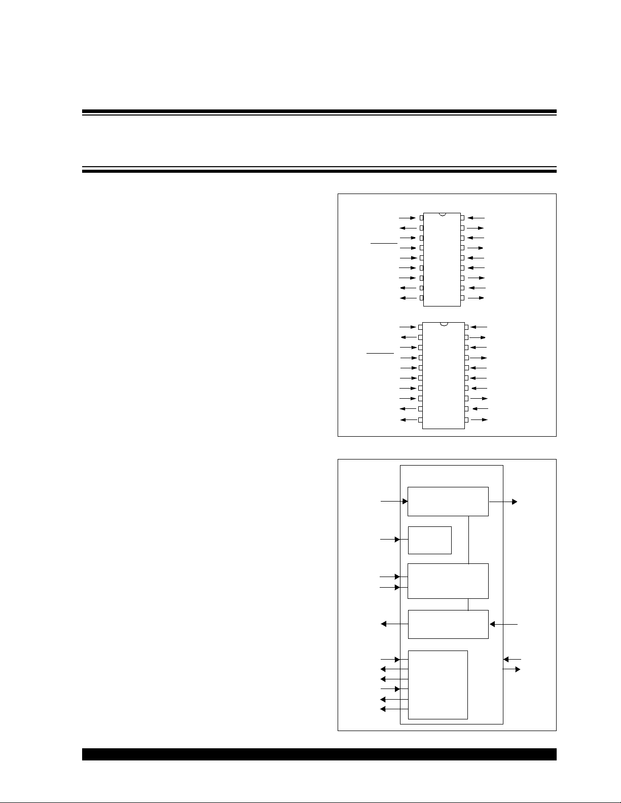
Package Types
PDIP, SOIC
18
1
2
3
4
5
6
7
8
9
1
2
3
4
5
6
7
8
9
10
17
16
MCP2150
15
14
13
12
11
10
20
19
18
MCP2150
17
16
15
14
13
12
11
SSOP
BAUD0
TXIR
RXIR
RESET
V
SS
EN
TX
RX
RI
BAUD0
TXIR
RXIR
RESET
V
SS
SS
V
EN
TX
RX
RI DSR
Block Diagram
MCP2150
TX TXIR
EN
BAUD1
BAUD0
RX
RTS
CTS
DSR
DTR
CD
RI
Encode and
Protocol Handler
Logic
Baud Rate
Generator
Protocol Handler
and Decode
UART
Control
BAUD1
CD
OSC1/CLKI
OSC2
DD
V
RTS
CTS
DTR
DSR
BAUD1
CD
OSC1/CLKI
OSC2
DD
V
DD
V
RTS
CTS
DTR
RXIR
OSC1
OSC2
2002 Microchip Technology Inc. Preliminary
DS21655B-page 1
Page 2

MCP2150
NOTES:
DS21655B-page 2
Preliminary 2002 Microchip Technology Inc.
Page 3

MCP2150
1.0 DEVICE OVERVIEW
This document contains device specific information for
the following device:
• MCP2150
The MCP2150 is a cost effective, low pin count (18-pin),
easy to use device for implementing IrDA standard wireless connectivity. The MCP2150 provides support for
the IrDA standard protocol “stack” plus bit encoding/
decoding.
The serial interface baud rates are user selectable to
one of four IrDA standard baud rates between 9600
baud and 115.2 kbaud (9600, 19200, 57600, 115200).
The IR baud rates are user selectable to one of five
IrDA standard baud rates between 9600 baud and
115.2 kbaud (9600, 19200, 37400, 57600, 115200).
The serial interface baud rate will be specified by the
BAUD1:BAUD0 pins, while the IR baud rate is specified
by the Primary Device (during Discover phase). This
means that the baud rates do not need to be the same.
The MCP2150 operates in Data Terminal Equipment
(DTE) applications and sits between a UART and an
infrared optical transceiver.
The MCP2150 encodes an asynchronous serial data
stream, converting each data bit to the corresponding
infrared (IR) formatted pulse. IR pulses received are
decoded and then handled by the protocol handler
state machine. The protocol handler sends the appropriate data bytes to the Host Controller in UART
formatted serial data.
The MCP2150 supports “point-to-point” applications.
That is, one Primary device and one Secondary device.
The MCP2150 operates as a Secondary device. It does
not support “multi-point” applications.
Sending data using IR light requires some hardware
and the use of specialized communication protocols.
These protocol and hardware requirements are
described, in detail, by the IrDA standard specifications. The encoding/decoding functionality of the
MCP2150 is designed to be compatible with the physical layer component of the IrDA standard. This part of
the standard is often referred to as “IrPHY”.
The complete IrDA standard specifications are available for download from the IrDA website
(www.IrDA.org).
2002 Microchip Technology Inc. Preliminary
DS21655B-page 3
Page 4
MCP2150
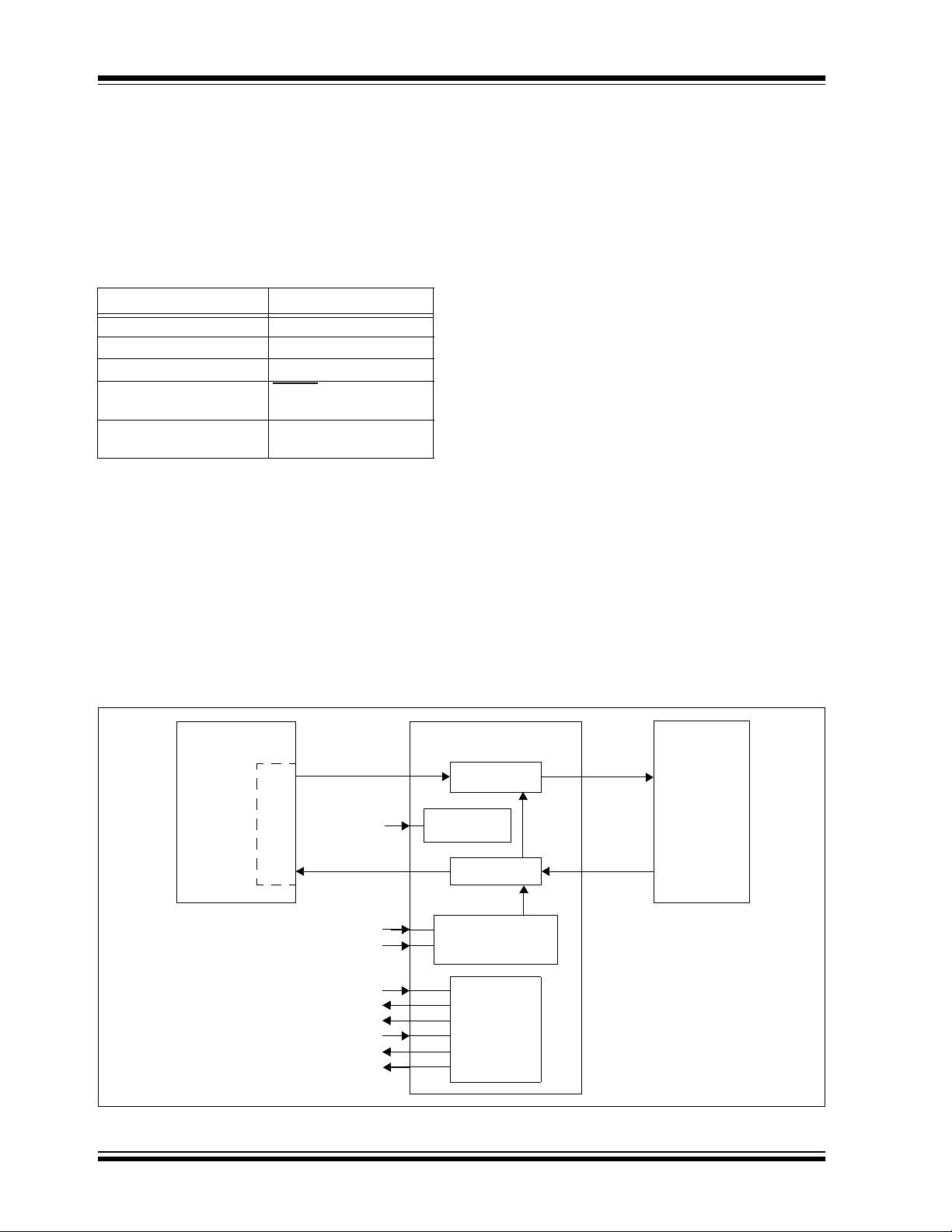
1.1 Applications
The MCP2150 Infrared Communications Controller
supporting the IrDA standard provides embedded system designers the easiest way to implement IrDA standard wireless connectivity. Figure 1-1 shows a typical
application block diagram. Table 1-2 shows the pin
definitions.
TABLE 1-1: OVERVIEW OF FEATURES
Features MCP2150
Serial Communications UART, IR
Baud Rate Selection Hardware
Low Power Mode Yes
Resets (and Delays) RESET
Packages 18-pin DIP, SOIC,
, POR
(PWRT and OST)
20-pin SSOP
Infrared communication is a wireless two-way data
connection, using infrared light generated by low-cost
transceiver signaling technology. This provides reliable
communication between two devices.
Infrared technology offers:
• Universal standard for connecting portable
computing devices
• Easy, effortless implementation
• Economical alternative to other connectivity
solutions
• Reliable, high-speed connection
• Safe to use in any environment (can even be
used during air travel)
• Eliminates the hassle of cables
• Allows PCs and other electronic devices (such as
PDAs, cell phones, etc.) to communicate with
each other
• Enhances mobility by allowing users to easily
connect
The MCP2150 allows the easy addition of IrDA standard wireless connectivity to any embedded application that uses serial data. Figure 1-1 shows typical
implementation of the MCP2150 in an embedded
system.
The IrDA protocols for printer support are not included
in the IrCOMM 9-wire “cooked” service class.
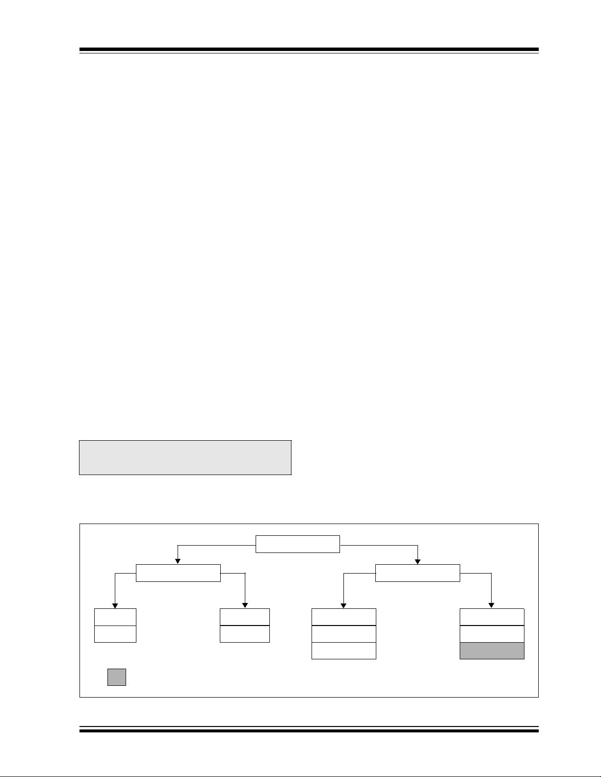
FIGURE 1-1: SYSTEM BLOCK DIAGRAM
Host Controller
(Microcontroller)
TX
UART
RX
EN
BAUD1
BAUD0
RTS
CTS
DSR
DTR
CD
RI
TX
RX
MCP2150
Encode
Power Down
Logic
Decode
Baud Rate
Generator
UART
Control
TXIR
RXIR
Optical
Transceiver
TXD
RXD
DS21655B-page 4
Preliminary 2002 Microchip Technology Inc.
Page 5

TABLE 1-2: PIN DESCRIPTIONS
MCP2150
Pin Name
BAUD0 1 1 1 I ST BAUD1:BAUD0 specify the baud rate of the device.
TXIR 2 2 2 O — Asynchronous transmit to Infrared transceiver.
RXIR 3 3 3 I ST Asynchronous receive from Infrared transceiver.
4 4 4 I ST Resets the device.
RESET
SS 5 5 5, 6 — P Ground reference for logic and I/O pins.
V
EN 6 6 7 I TTL Device enable.
TX 7 7 8 I TTL Asynchronous receive; from Host Controller UART.
RX 8 8 9 O — Asynchronous transmit; to Host Controller UART.
RI 9 9 10 — — Ring Indicator. The value on this pin is driven high.
DSR 10 10 11 O — Data Set Ready. Indicates that the MCP2150 has completed
DTR 11 11 12 I TTL Data Terminal Ready. The value of this pin is ignored once
CTS 12 12 13 O — Clear to Send. Indicates that the MCP2150 is ready to
RTS 13 13 14 I TTL Request to Send. Indicates that a Host Controller is ready to
V
DD
14 14 15, 16 — P Positive supply for logic and I/O pins.
OSC2 15 15 17 O — Oscillator crystal output.
OSC1/CLKIN 16 16 18 I CMOS Oscillator crystal input/external clock source input.
CD 17 17 19 O — Carrier Detect. Indicates that the MCP2150 has established a
BAUD1 18 18 20 I ST BAUD1:BAUD0 specify the baud rate of the device.
Legend: TTL = TTL compatible input
I = Input
P = Power
Pin Number
PDIP SOIC SSOP
Pin
Buffer
Type
Type
1 = Device is enabled.
0 = Device is disabled (low power). MCP2150 only monitors
this pin when in the NDM state.
reset.
1 = MCP2150 is initialized.
0 = MCP2150 is not initialized.
the MCP2150 is initialized. It is recommended that this pin be
connected so that the voltage level is either V
device power up, this signal is used with the RTS signal to
enter device ID programming.
1 = Enter Device ID programming mode (if RTS is cleared).
0 = Do not enter Device ID programming mode.
receive data from the Host Controller.
1 = Host Controller should not send data.
0 = Host Controller may send data.
receive data from the MCP2150. The MCP2150 prepares to
send data, if available.
1 = Host Controller not ready to receive data.
0 = Host Controller ready to receive data.
At device power up, this signal is used with the DTR signal to
enter device ID programming.
1 = Do not enter Device ID programming mode.
0 = Enter Device ID programming mode (if DTR is set).
valid link with a Primary Device.
1 = An IR link has not been established (No IR Link).
0 = An IR link has been established (IR Link).
ST = Schmitt Trigger input with CMOS levels
O = Output
CMOS = CMOS compatible input
Description
SS or VCC. At
2002 Microchip Technology Inc. Preliminary
DS21655B-page 5
Page 6

MCP2150
1.1.1 SIGNAL DIRECTIONS
Table 1-3 shows the direction of the MCP2150 signals.
The MCP2150 is designed for use in Data Terminal
Equipment (DTE) applications.
TABLE 1-3: MCP2150 S IGNAL DIRECTION
DB-9
Pin No.
Legend: HC = Host Controller
Note 1: This signal is not implemented in the MCP2150.
Signal Direction Comment
1 CD MCP2150 → HC Carrier Detect
2 RX MCP2150 → HC Received Data
3 TX HC → MCP2150 Transmit Data
4DTR
5 GND — Ground
6 DSR MCP2150 → HC Data Set Ready
7 RTS HC → MCP2150 R equest to Send
8 CTS MCP2150 → HC Clear to Send
9RI
(1)
(1)
— Ring Indicator
— Data Terminal
Ready
DS21655B-page 6
Preliminary 2002 Microchip Technology Inc.
Page 7
MCP2150
2.0 DEVICE OPERATION
The MCP2150 is a cost effective, low pin count (18pin), easy to use device for implementing IrDA standard wireless connectivity. The MCP2150 provides
support for the IrDA standard protocol “stack” plus bit
encoding/decoding. The Serial interface and IR baud
rates are independantly selectable.
2.1 Power Up
Any time the device is powered up (parameter D003),
the Power Up Timer delay (parameter 33) occurs, followed by an Oscillator Start-up Timer (OST) delay
(parameter 32). Once these delays complete, communication with the device may be initiated. This communication is from both the infrared transceiver’s side as
well as the controller’s UART interface.
2.2 Device Reset
The MCP2150 is forced into the reset state when the
RESET
pin is in the low state. Once the RESET pin is
brought to a high state, the Device Reset sequence
occurs. Once the sequence completes, functional
operation begins.
2.3 Clock Source
The MCP2150 requires a clock source to operate. The
frequency of this clock is 11.0592 MHz (electrical specification parameter 1A). This clock can be supplied by
either a crystal/resonator or as an external clock input.
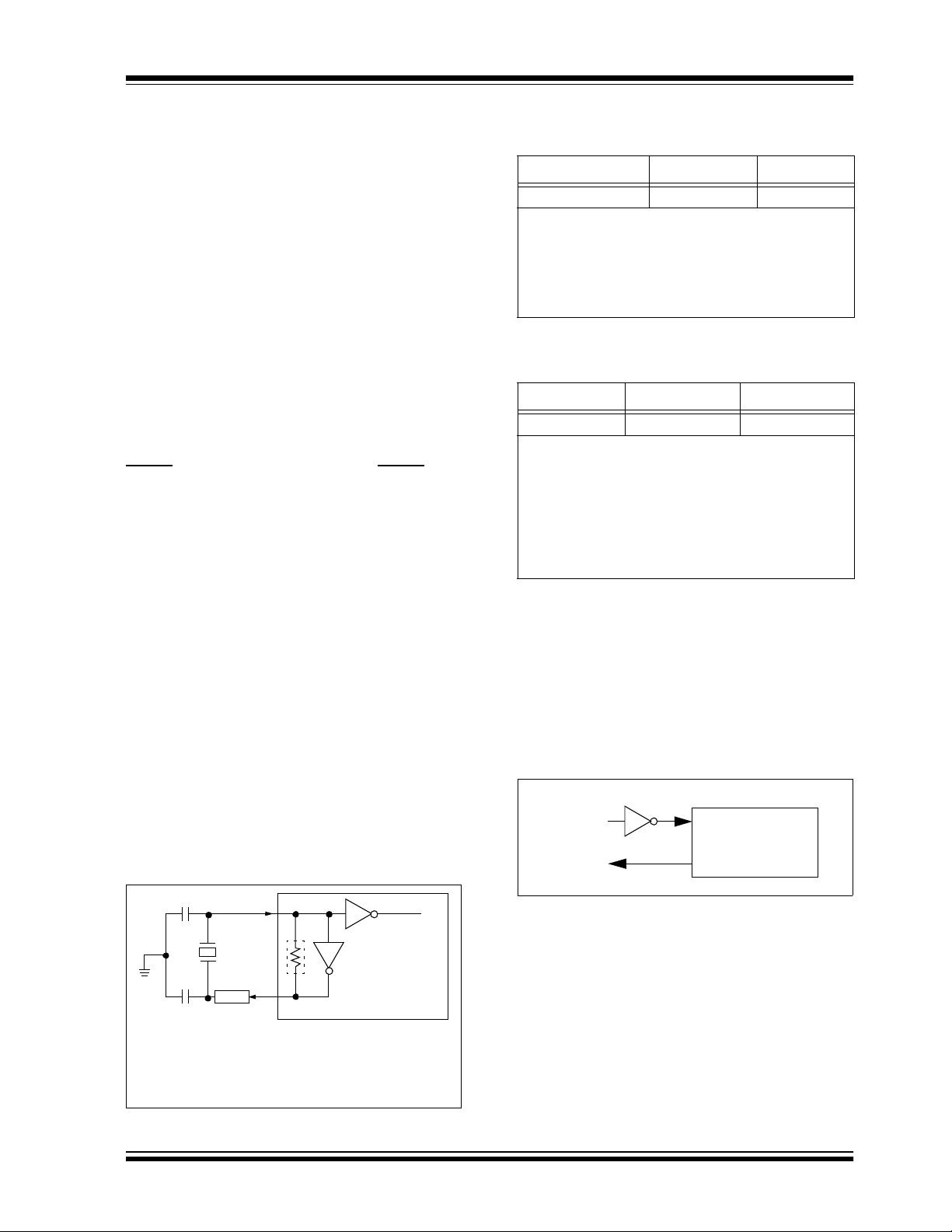
2.3.1 CRYSTAL OSCILLATOR / CERAMIC
RESONATORS
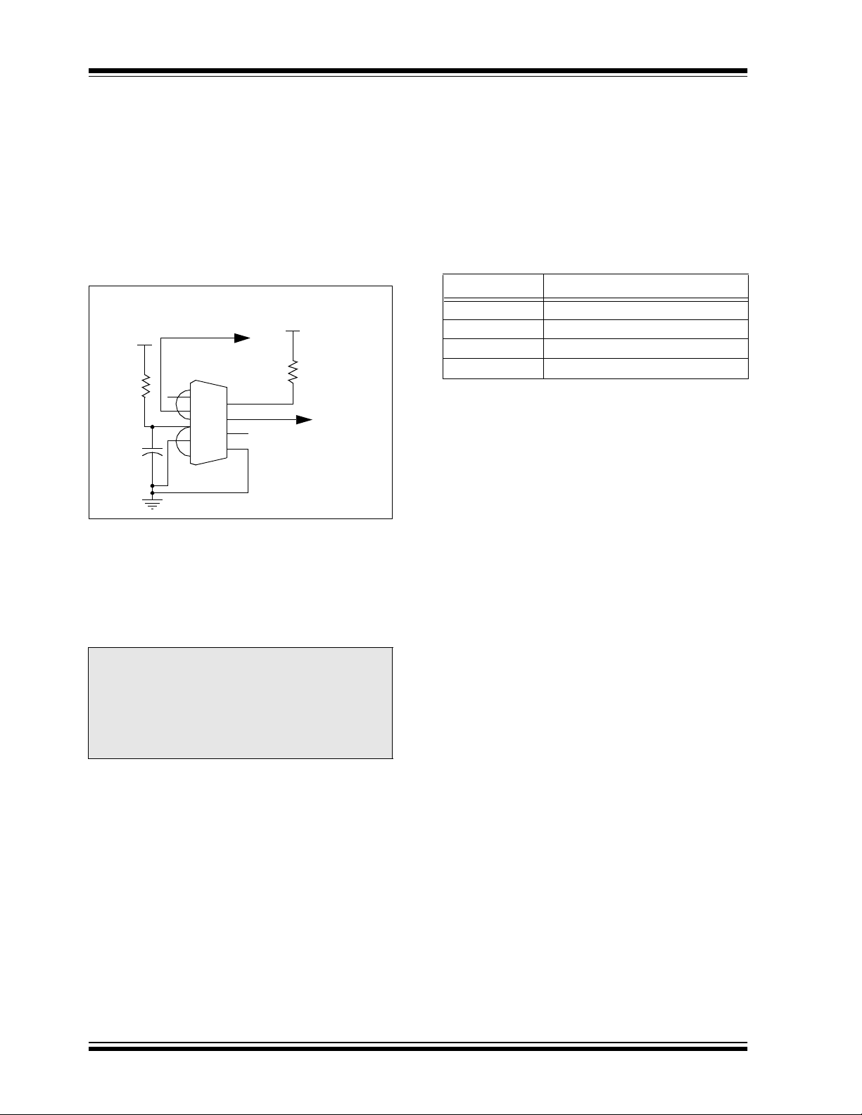
A crystal or ceramic resonator can be connected to the
OSC1 and OSC2 pins to establish oscillation
(Figure 2-1). The MCP2150 oscillator design requires
the use of a parallel cut crystal. Use of a series cut crystal may give a frequency outside of the crystal
manufacturers specifications.
FIGURE 2-1: CRYSTAL OPERATION
(OR CERAMIC
RESONATOR)
TABLE 2-1: CAPACITOR SELECTION FOR
CERAMIC RESONATORS
Freq OSC1 (C1) OSC2 (C2)
11.0592 MHz 10 - 22 pF 10 - 22 pF
Higher capacitance increases the stability of the oscillator but also increases the start-up time. These values are for design guidance only. Since each
resonator has its own characteristics, the user should
consult the resonator manufacturer for appropriate
values of external components.
TABLE 2-2: CAPACITOR SELECTION FOR
CRYSTAL OSCILLATOR
Freq OSC1 (C1) OSC2 (C2)
11.0592 MHz 15 - 30 pF 15 - 30 pF
Higher capacitance increases the stability of the oscillator but also increases the start-up time. These values are for design guidance only. R
to avoid overdriving crystals with low drive level specification. Since each crystal has its own
characteristics, the user should consult the crystal
manufacturer for appropriate values of external
components.
S may be required
2.3.2 EXTERNAL CLOCK IN
For applications where a clock is already available
elsewhere, users may directly drive the MCP2150 provided that this external clock source meets the AC/DC
timing requirements listed in Section 4.3. Figure 2-2
shows how an external clock circuit should be
configured.
FIGURE 2-2: EXTERNAL CLOCK INPUT
OPERATION
Clock From
external
system
Open
OSC1
MCP2150
OSC2
OSC1
C1
XTAL
OSC2
RS
Note
C2
See Tab le 2 -1 and Tab le 2- 2 for recommended values of
C1 and C2.
Note: A series resistor may be required for AT
strip cut crystals.
2002 Microchip Technology Inc. Preliminary
RF
To internal
logic
MCP2150
DS21655B-page 7
Page 8

MCP2150
2.4 Bit Clock
The device crystal is used to derive the communication
bit clock (BITCLK). There are 16 BITCLKs for each bit
time. The BITCLKs are used for the generation of the
start bit and the eight data bits. The stop bit uses the
BITCLK when the data is transmitted (not for
reception).
This clock is a fixed frequency and has minimal
variation in frequency (specified by crystal
manufacturer).
2.5 UART Interface
The UART interface communicates with the "controller". This interface is a half duplex interface, meaning
that the system is either transmitting or receiving, but
not both simultaneously.
2.5.1 BAUD RATE
The baud rate for the MCP2150 serial port (the TX and
RX pins) is configured by the state of the BAUD1 and
BAUD0 pins. These two device pins are used to select
the baud rate at which the MCP2150 will transmit and
receive serial data (not IR data). Table 2-3 shows the
baud rate configurations.
TABLE 2-3: SERIAL BAUD RATE
SELECTION VS. FREQUENCY
BAUD1:BAUD0
00 9600 F
01 19200 F
10 57600 F
11 115200 F
Baud Rate @
11.0592 MHz
Bit Rate
OSC / 1152
OSC / 576
OSC / 192
OSC / 96
2.5.2 TRANSMITTING
When the controller sends serial data to the MCP2150,
the controller’s baud rate is required to match the baud
rate of the MCP2150’s serial port.
2.5.3 RECEIVING
When the controller receives serial data from the
MCP2150, the controller’s baud rate is required to
match the baud rate of the MCP2150’s serial port.
DS21655B-page 8
Preliminary 2002 Microchip Technology Inc.
Page 9
MCP2150
2.6 Modulation
The data that the MCP2150 UART received (on the TX
pin) that needs to be transmitted (on the TXIR pin) will
need to be modulated. This modulated signal drives the
IR transceiver module. Figure 2-3 shows the encoding
of the modulated signal.
Note: The signal on the TXIR pin does not actu-
ally line up in time with the bit value that
was transmitted on the TX pin, as shown in
Figure 2-3. The TX bit value is shown to
represent the value to be transmitted on
the TXIR pin.
Each bit time is comprised of 16-bit clocks. If the value
to be transmitted (as determined by the TX pin) is a
logic low, then the TXIR pin will output a low level for
7-bit clock cycles, a logic high level for 3-bit clock
cycles or a minimum of 1.6 µsec. (see parameter
IR121). The remaining 6-bit clock cycles will be low. If
the value to transmit is a logic high, then the TXIR pin
will output a low level for the entire 16-bit clock cycles.
FIGURE 2-3: ENCODING
2.7 Demodulation
The modulated signal (data) from the IR transceiver
module (on RXIR pin) needs to be demodulated to form
the received data (on RX pin). Once demodulation of
the data byte occurs, the data that is received is transmitted by the MCP2150 UART (on the RX pin).
Figure 2-4 shows the decoding of the modulated
signal.
Note: The signal on the RX pin does not actually
line up in time with the bit value that was
received on the RXIR pin, as shown in
Figure 2-4. The RXIR bit value is shown to
represent the value to be transmitted on
the RX pin.
Each bit time is comprised of 16-bit clocks. If the value
to be received is a logic low, then the RXIR pin will be
a low level for the first 3-bit clock cycles or a minimum
of 1.6 µs. The remaining 13-bit clock cycles (or difference up to the 16-bit clock time) will be high. If the value
to be received is a logic high, then the RXIR pin will be
a high level for the entire 16-bit clock cycles. The level
on the RX pin will be in the appropriate state for the
entire 16 clock cycles.
Start Bit Data bit 0 Data bit 1 Data bit 2 Data bit ...
16 CLK
BITCLK
TX Bit
Value
TXIR
7 CLK
24 Tosc
0100 01
FIGURE 2-4: DECODING
Start Bit Data bit 0 Data bit 1 Data bit 2 Data bit ...
16 CLK
BITCLK
(CLK)
RXIR Bit
Valu e
RX
≥ 1.6 µs (up to 3 CLK)
16 CLK 16 CLK 16 CLK 16 CLK 16 CLK 16 CLK
≥ 13 CLK
0100 01
2002 Microchip Technology Inc. Preliminary
DS21655B-page 9
Page 10

MCP2150
2.8 Minimizing Power
The device can be placed in a low power mode by disabling the device (holding the EN pin at the low state).
The internal state machine is monitoring this pin for a
low level and, once this is detected, the device is
disabled and enters into a low power state.
2.8.1 RETURNING TO DEVICE
OPERATION
When disabled, the device is in a low power state.
When the EN pin is brought to a high level, the device
will return to the operating mode. The device requires
a delay of 1024 T
or received.
FIGURE 2-5: ISO REFERENCE LAYER MODEL
OSC before data may be transmitted
OSI REFERENCE LAYERS
Application
Presentation
Session
Transport
Network
Data Link Layer
2.9 Network Layering Reference Model
Figure 2-5 shows the ISO Network Layering Reference
Model. The shaded areas are implemented by the
MCP2150, the cross-hatched area is implemented by
an infrared transceiver. The unshaded areas should be
implemented by the Host Controller.
Has to be implemented in Host
Controller firmware
(such as a PICmicro
microcontroller)
Regions implemented
by the MCP2150
Regions implemented
by the Optical Transceiver logic
®
LLC (Logical Link Control)
Acceptance Filtering
Overload Notification
Recovery Management
MAC (Medium Access Control)
Data Encapsulation/Decapsulation
Frame Coding (stuffing, destuffing)
Medium Access Management
Error Detection
Error Signalling
Acknowledgment
Serialization/Deserialization
Physical Layer
PLS (Physical Signalling)
Bit Encoding/Decoding
Bit Timing
Synchronization
PMA (Physical Medium Attachment)
Driver/Receiver Characteristics
MDI (Medium Dependent Interface)
Connectors
Supervisor
Fault
confinement
(MAC-LME)
Bus Failure
management
(PLS-LME)
DS21655B-page 10
Preliminary 2002 Microchip Technology Inc.
Page 11

MCP2150
The IrDA standard specifies the following protocols:
• Physical Signaling Layer (PHY)
• Link Access Protocol (IrLAP)
• Link Management Protocol/Information Access
Service (IrLMP/IAS)
The IrDA data lists optional protocols. They are:
•Tiny TP
• IrTran-P
• IrOBEX
•IrLAN
•IrCOMM
•IrMC
•IrDA Lite
Figure 2-6 shows the IrDA data protocol stack and
which components are implemented by the MCP2150.
FIGURE 2-6: IRDA DATA - PROTOCOL
STACKS
IrTran-P IrObex IrLan IrMC
LM-IAS Tiny Transport Protocol (Tiny TP)
IR Link Management - Mux (IrLMP)
IR Link Access Protocol (IrLAP)
Asynchronous
Serial IR
(9600 -115200 b/s)
Supported by
the MCP2150
(2)
Synchronous
IrComm
Serial IR
(1.152 Mb/s)
Optional IrDA data
protocols not
supported by
the MCP2150
(1)
Synchronous
4 PPM
(4 Mb/s)
2.9.1 IrDA DATA PROTOCOLS
SUPPORTED BY MCP2150
The MCP2150 supports these required IrDA standard
protocols:
• Physical Signaling Layer (PHY)
• Link Access Protocol (IrLAP)
• Link Management Protocol/Information Access
Service (IrLMP/IAS)
The MCP2150 also supports some of the optional protocols for IrDA data. The optional protocols that the
MCP2150 implements are:
•Tiny TP
•IrCOMM
2.9.1.1 Physical Signal Layer (PHY)
The MCP2150 provides the following Physical Signal
Layer specification support:
• Bidirectional communication
• Data Packets are protected by a CRC
- 16-bit CRC for speeds up to 115.2 kbaud
• Data Communication Rate
- 9600 baud minimum data rate
The following Physical Layer Specification is dependant on the optical transceiver logic used in the
application. The specification states:
• Communication Range, which sets the end user
expectation for discovery, recognition and performance.
- Continuous operation from contact to at least
1 meter (typically 2 meters can be reached)
- A low power specification reduces the objective for operation from contact to at least
20 cm (low power and low power) or 30 cm
(low power and standard power).
Note 1: The MCP2155 implements the 9-wire
“cooked" service class serial replicator.
2: An optical transceiver is required.
2002 Microchip Technology Inc. Preliminary
DS21655B-page 11
Page 12

MCP2150
2.9.1.2 IrLAP
The MCP2150 supports the IrLAP protocol. The IrLAP
protocol provides:
• Management of communication processes on the
link between devices.
• A device-to-device connection for the reliable,
ordered transfer of data.
• Device discover procedures.
• Hidden node handling.
Figure 2-7 identifies the key parts and hierarchy of the
IrDA protocols. The bottom layer is the Physical layer,
IrPHY. This is the part that converts the serial data to
and from pulses of IR light. IR transceivers can’t transmit and receive at the same time. The receiver has to
wait for the transmitter to finish sending. This is sometimes referred to as a “Half-Duplex” connection. The IR
Link Access Protocol (IrLAP) provides the structure for
packets (or “frames”) of data to emulate data that would
normally be free to stream back and forth.
FIGURE 2-7: IRDA STANDARD
PROTOCOL LAYERS
Host O.S. or Application
IrCOMM
IrLMP – IAS
IrLAP
Protocols
resident in
MCP2150
Figure 2-8 shows how the IrLAP frame is organized.
The frame is proceeded by some number of Beginning
of Frame characters (BOFs). The value of the BOF is
generally 0xC0, but 0xFF may be used if the last BOF
character is a 0xC0. The purpose of multiple BOFs is to
give the other station some warning that a frame is
coming.
The IrLAP frame begins with an address byte (“A”
field), then a control byte (“C” field). The control byte is
used to differentiate between different types of frames
and is also used to count frames. Frames can carry status, data or commands. The IrLAP protocol has a command syntax of it’s own. These commands are part of
the control byte. Lastly, IrLAP frames carry data. This
data is the information (or “I”) field. The integrity of the
frame is ensured with a 16-bit CRC, referred to as the
Frame Check Sequence (FCS). The 16-bit CRC value
is transmitted LSB first. The end of the frame is marked
with an EOF character, which is always a 0xC1. The
frame structure described here is used for all versions
of IrDA protocols used for serial wire replacement for
speeds up to 115.2 kbaud.
Note 1: Another IrDA standard that is entering
general usage is IR Object Exchange
(IrOBEX). This standard is not used for
serial connection emulation.
2: IrDA communication standards faster
than 115.2 kbaud use a different CRC
method and physical layer.
FIGURE 2-8: IRLAP FRAME
IrPHY
IR pulses
transmitted
and
received
X BOFs BOF A C FCSI EOF
2
(1+N) of C0h payload
In addition to defining the frame structure, IrLAP provides the “housekeeping” functions of opening, closing
and maintaining connections. The critical parameters
that determine the performance of the link are part of
this function. These parameters control how many
BOFs are used, identify the speed of the link, how fast
either party may change from receiving to transmitting,
etc. IrLAP has the responsibility of negotiating these
parameters to the highest common set so that both
sides can communicate as quickly, and as reliably, as
possible.
bytes
C1h
DS21655B-page 12
Preliminary 2002 Microchip Technology Inc.
Page 13
MCP2150
2.9.1.3 IrLMP
The MCP2150 implements the IrLMP protocol. The
IrLMP protocol provides:
• Multiplexing of the IrLAP layer. This allows multiple channels above an IrLAP connection.
• Protocol and service discovery. This is via the
Information Access Service (IAS).
When two devices that contain the IrDA standard feature are connected, there is generally one device that
has something to do and the other device that has the
resource to do it. For example, a laptop may have a job
to print and an IrDA standard compatible printer has the
resources to print it. In IrDA standard terminology, the
laptop is a Primary device and the printer is the Secondary device. When these two devices connect, the
Primary device must determine the capablities of the
Secondary device to determine if the Secondary device
is capable of doing the job. This determination is made
by the Primary device asking the Secondary device a
series of questions. Depending on the answers to
these questions, the Primary device may or may not
elect to connect to the Secondary device.
The queries from the Primary device are carried to the
Secondary device using IrLMP. The responses to these
queries can be found in the Information Access Service
(IAS) of the Secondary device. The IAS is a list of the
resources of the Secondary device. The Primary
device compares the IAS responses with its requirements and then makes the decision if a connection
should be made.
The MCP2150 identifies itself to the Primary device as
a modem.
2.9.1.4 Link Management - Information
Access Service (LM-IAS)
The MCP2150 implements the LM-IAS. Each LM-IAS
entity maintains an information database to provide:
• Information on services for other devices that
contain the IrDA standard feature (Discovery).
• Information on services for the device itself.
• Remote accessing of another device’s information
base.
This is required so that clients on a remote device can
find configuration information needed to access a
service.
2.9.1.5 Tiny TP
Tiny TP provides the flow control on IrLMP connections. An optional service of Segmentation and
Reassembly can be handled.
2.9.1.6 IrCOMM
IrCOMM provides the method to support serial and parallel port emulation. This is useful for legacy COM
applications, such as printers and modem devices.
The IrCOMM standard is just a syntax that allows the
Primary device to consider the Secondary device as a
serial device. IrCOMM allows for emulation of serial or
parallel (printer) connections of various capabilities.
The MCP2150 supports the 9-wire “cooked” service
class of IrCOMM. Other service classes supported by
IrCOMM are shown in Figure 2-9.
Note: The MCP2150 identifies itself as a modem
to ensure that it is identified as a serial
device with a limited amount of memory.
The MCP2150 is not a modem, and the non-data circuits are not handled in a modem fashion.
FIGURE 2-9: IRCOMM SERVICE CLASSES
IrCOMM Services
Uncooked Services Cooked Services
Parallel Serial
IrLPT
Supported by MCP2150
3-wire Raw
Parallel
Centronics
IEEE 1284
Serial
3-wire Cooked
9-wire Cooked
2002 Microchip Technology Inc. Preliminary
DS21655B-page 13
Page 14

MCP2150
2.9.2 OTHER OPTIONAL IrDA DATA
PROTOCOLS
Other IrDA data protocols have been developed to specific application requirements. These optional protocols
are not supported by the MCP2150. These IrDA data
protocols are briefly described in the following sub-sections. For additional information, please refer to the
IrDA website (www.IrDA.org).
2.9.2.1 IrTran-P
IrTran-P provides the protocol to exchange images with
digital image capture devices/cameras.
2.9.2.2 IrOBEX
IrOBEX provides OBject EXchange services. This is
similar to HTTP.
2.9.2.3 IrLAN
IrLAN describes a protocol to support IR wireless
access to a Local Area Network (LAN).
2.9.2.4 IrMC
IrMC describes how mobile telephony and communication devices can exchange information. This information includes phonebook, calender and message data.
Also how call control and real-time voice are handled
(RTCON).
2.9.2.5 IrDA Lite
IrDA Lite describes how to reduce the application code
requirements, while maintaining compatibility with the
full implementation.
DS21655B-page 14
Preliminary 2002 Microchip Technology Inc.
Page 15

MCP2150
2.9.3 HOW DEVICES CONNECT
When two devices implementing the IrDA standard feature establish a connection using the IrCOMM protocol,
the process is analogous to connecting two devices
with serial ports using a cable. This is referred to as a
"point-to-point" connection. This connection is limited
to half-duplex operation because the IR transceiver
cannot transmit and receive at the same time. The purpose of the IrDA protocol is to allow this half-duplex link
to emulate, as much as possible, a full-duplex connection. In general, this is done by dividing the data into
“packets”, or groups of data. These packets can then
be sent back and forth, when needed, without risk of
collision. The rules of how and when these packets are
sent constitute the IrDA protocols. The MCP2150 supports elements of this IrDA protocol to communicate
with other IrDA standard compatible devices.
When a wired connection is used, the assumption is
made that both sides have the same communications
parameters and features. A wired connection has no
need to identify the other connector because it is
assumed that the connectors are properly connected.
In the IrDA standard, a connection process has been
defined to identify other IrDA compatible devices and
establish a communication link. There are three steps
that these two devices go through to make this
connection. They are:
• Normal Disconnect Mode (NDM)
• Discovery Mode
• Normal Connect Mode (NCM)
Figure 2-10 shows the connection sequence.
2.9.3.1 Normal Disconnect Mode (NDM)
When two IrDA standard compatible devices come into
range they must first recognize each other. The basis
of this process is that one device has some task to
accomplish and the other device has a resource
needed to accomplish this task. One device is referred
to as a Primary device and the other is referred to as a
Secondary device. This distinction between Primary
device and Secondary device is important. It is the
responsibility of the Primary device to provide the
mechanism to recognize other devices. So the Primary
device must first poll for nearby IrDA standard compatible devices. During this polling, the defaut baud rate of
9600 baud is used by both devices.
For example, if you want to print from an IrDA
equipped laptop to an IrDA printer, utilizing the IrDA
standard feature, you would first bring your laptop in
range of the printer. In this case, the laptop is the one
that has something to do and the printer has the
resource to do it. The laptop is called the Primary
device and the printer is the Secondary device. Some
data-capable cellphones have IrDA standard infrared
ports. If you used such a cellphone with a Personal Dig-
ital Assistant (PDA), the PDA that supports the IrDA
standard feature would be the Primary device and the
cellphone would be the Secondary device.
When a Primary device polls for another device, a
nearby Secondary device may respond. When a Secondary device responds, the two devices are defined to
be in the Normal Disconnect Mode (NDM) state. NDM
is established by the Primary device broadcasting a
packet and waiting for a response. These broadcast
packets are numbered. Usually 6 or 8 packets are sent.
The first packet is number 0, the last packet is usually
number 5 or 7. Once all the packets are sent, the Primary device sends an ID packet, which is not numbered.
The Secondary device waits for these packets and then
responds to one of the packets. The packet it responds
to determines the “time slot” to be used by the Secondary device. For example, if the Secondary device
responds after packet number 2, then the Secondary
device will use time slot 2. If the Secondary device
responds after packet number 0, then the Secondary
device will use time slot 0. This mechanism allows the
Primary device to recognize as many nearby devices
as there are time slots. The Primary device will continue to generate time slots and the Secondary device
should continue to respond, even if there’s nothing to
do.
Note 1: The MCP2150 can only be used to
implement a Secondary device.
2: The MCP2150 supports a system with
only one Secondary device having exclusive use of the IrDA standard infrared link
(known as "point-to-point" communication).
3: The MCP2150 always responds to packet
number 2. This means that the MCP2150
will always use time slot 2.
4: If another Secondary device is nearby,
the Primary device may fail to recognize
the MCP2150, or the Primary device may
not recognize either of the devices.
During NDM, the MCP2150 handles all of the
responses to the Primary device (Figure 2-10) without
any communication with the Host Controller. The Host
Controller is inhibited by the CTS signal of the
MCP2150 from sending data to the MCP2150.
2002 Microchip Technology Inc. Preliminary
DS21655B-page 15
Page 16

MCP2150
2.9.3.2 Discovery Mode
Discovery mode allows the Primary device to determine the capabilities of the MCP2150 (Secondary
device). Discovery mode is entered once the MCP2150
(Secondary device) has sent an XID response to the
Primary device and the Primary device has completed
sending the XIDs and then sends a Broadcast ID. If this
sequence is not completed, then a Primary and
Secondary device can stay in NDM indefinitely.
When the Primary device has something to do, it
initiates Discovery. Discovery has two parts. They are:
• Link initialization
• Resource determination
The first step is for the Primary and Secondary devices
to determine, and then adjust to, each other’s hardware
capabilities. These capabilities are parameters like:
• Data rate
• Turn around time
• Number of packets without a response
• How long to wait before disconnecting
Both the Primary and Secondary device begin communications at 9600 baud, which is the default baud rate.
The Primary device sends its parameters, then the
Secondary device responds with its parameters. For
example, if the Primary supports all data rates up to
115.2 kbaud and the Secondary device only supports
19.2 kbaud, the link will be established at 19.2 kbaud.
Note: The MCP2150 is limited to a data rate of
115.2 kbaud.
Once the hardware parameters are established, the
Primary device must determine if the Secondary device
has the resources it requires. If the Primary device has
a job to print, then it must know if it’s talking to a printer,
not a modem or other device. This determination is
made using the Information Access Service (IAS). The
job of the Secondary device is to respond to IAS queries made by the Primary device. The Primary device
must ask a series of questions like:
• What is the name of your service?
• What is the address of this service?
• What are the capabilities of this device?
When all the Primary device’s questions are answered,
the Primary device can access the service provided by
the Secondary device.
During Discovery mode, the MCP2150 handles all
responses to the Primary device (see Figure 2-10)
without any comm unication with the Host Controller.
The Host Controller is inhibited by the CTS signal of the
MCP2150 from sending data to the MCP2150.
2.9.3.3 Normal Connect Mode (NCM)
Once discovery has been completed, the Primary
device and MCP2150 (Secondary device) can freely
exchange data.
The MCP2150 can receive IR data or serial data, but
not both simultaneously. The MCP2150 uses a hardware handshake to stop the local serial port from
sending data while the MCP2150 is receiving IR data.
Note: Data loss will result if this hardware
handshake is not observed.
Both the Primary device and the MCP2150 (Secondary
device) check to make sure that data packets are
received by the other without errors. Even when data is
required to be sent, the Primary and Secondary
devices will still exchange packets to ensure that the
connection hasn’t, unexpectedly, been dropped. When
the Primary device has finished, it then transmits the
close link command to the MCP2150 (Secondary
device). The MCP2150 will confirm the close link command and both the Primary device and the MCP2150
(Secondary device) will revert to the NDM state.
Note: If the NCM mode is unexpectedly termi-
nated for any reason (including the Primary
device not issuing a close link command),
the MCP2150 will revert to the NDM state
10 seconds after the last frame has been
received.
It is the responsability of the Host Controller program to
understand the meaning of the data received and how
the program should respond to it. It’s just as if the data
were being received by the Host Controller from a
UART.
DS21655B-page 16
Preliminary 2002 Microchip Technology Inc.
Page 17

FIGURE 2-10: CONNECTION SEQUENCE
Primary Device Secondary Device
Normal Disconnect Mode (NDM)
Send XID Commands
(timeslots n, n+1, ...)
(approximately 70ms
between XID commands)
Finish sending XIDs
(max timeslots - y frames)
Broadcast ID
MCP2150
(ex. MCP2150)
No Response
XID Response in timeslot y,
claiming this timeslot, (MCP2150
always claims timeslot 2)
No Response to these XIDs
No Response to Broadcast ID
Discovery
Normal Response Mode (NRM)
Send SNRM Command
(w/ parameters and
connection address)
Open channel for IAS Queries
Send IAS Queries
Open channel for data
Send Data or Status
Send Data or Status
UA response with parameters
using connect address
Confirm channel open for IAS
Provide IAS responses
Confirm channel open for data
(MCP2150 CD pin driven low)
Send Data or Status
Send Data or Status
Shutdown link
2002 Microchip Technology Inc. Preliminary
Confirm shutdown
(back to NDM state)
DS21655B-page 17
Page 18

MCP2150
2.10 Operation
The MCP2150 emulates a null modem connection. The
application on the DTE device sees a virtual serial port.
This serial port emulation is provided by the IrDA standard protocols. The link between the DTE device and
the embedded application is made using the
MCP2150. The connection between the MCP2150 and
the embedded application is wired as if there were a
null modem connection.
The Carrier Detect (CD) signal of the MCP2150 is used
to indicate that a valid IrDA standard infrared link has
been established between the MCP2150 and the Primary device. The CD signal should be monitored
closely to make sure that any communication tasks can
be completed. The MCP2150 DSR signal indicates that
the device has powered-up, successfully initialized and
is ready for service. This signal is intended to be connected to the DSR input of the Host Controller. If the
Host Controller was directly connected to an IrDA standard Primary device using a serial cable (the MCP2150
is not present), the Host Controller would be connected
to the Primary device’s DTR output signal.
The MCP2150 generates the CTS signal locally
because of buffer limitations.
Note 1: The MCP2150 generates non-data
signals locally.
2: Only transceiver’s TXD and RXD signals
are carried back and forth to the Primary
device. The MCP2150 emulates a 3-wire
serial connection (TXD, RXD and GND).
2.10.1 HARDWARE HANDSHAKING
2.10.2 BUFFERS AND THROUGHPUT
The maximum IR data rate of the MCP2150 is
115.2 kbaud. The actual throughput will be less, due to
several factors. The most significant factors are under
the control of the developer. One factor beyond the
control of the designer is the overhead associated with
the IrDA standard. The MCP2150 uses a fixed data
block size of 64 bytes. To carry 64 bytes of data, the
MCP2150 must send 72 bytes (64+8). The additional 8
bytes are used by the protocol. When the Primary
device receives the frame, it must wait for a minimum
latency period before sending a packet of its own. This
turnaround time is set by IrLAP when the parameters of
the link are negotiated. A common turnaround time is
1 ms, although longer and shorter times may be
encountered. 1 ms represents approximately 12 byte
times at a data rate of 115.2 kbaud. The minimum size
frame the Primary device can respond with is 6 bytes.
The MCP2150 will add the 12 byte-time latency on its
own, again assuming a 1 ms latency. This means that
the maximum throughput will be 64 data bytes out of a
total of 64 + 38 byte times. Thus, the maximum theoretical throughput will be limited to about 64/(64+38)=63%
of the IR data rate. Actual maximum throughput will be
dependent on both the MCP2150 and the
characteristics of the Primary device.
The most significant factor in data throughput is how
well the data frames are filled. If only 1 byte is sent at a
time, then the maximum throughput is 1/(1+38)=2.5%
of the IR data rate. The best way to maximize throughput is to align the amounts of data with the packet size
of the MCP2150. Throughput examples are shown in
Table 2-4.
The MCP2150 uses a 64-byte buffer for incoming data
from the IR Host. Another 64-byte buffer is provided to
buffer data from the UART serial port. When an IR
packet begins the IrComm, the MCP2150 handles IR
data exclusively (the UART serial port buffer is not
available). A hardware handshaking pin (CTS) is provided to inhibit the Host Controller from sending serial
data while IR Data is being sent or received.
Note: When the CTS output from the IrComm is
high, no data should be sent from the Host
Controller. The UART FIFO will store up to
2 bytes. Any additional data bytes will be
lost.
Note: IrDA throughput is based on many factors
associated with characteristics of the Primary and Secondary devices. These characteristics may cause your application
throughput to be less than the theoretical
example shown in Tab le 2- 4.
TABLE 2-4: THEORETICAL IrDA STANDARD THROUGHPUT EXAMPLES @ 115.2 KBAUD
MCP2150
Data Packet
Size (Bytes)
64 8 6 12 12 102 62.7%
18 6 12 12 392.6%
Note 1: Number of bytes calculated based on a common turnaround time of 1 ms.
Overhead
(Bytes)
Primary Device
Minimum
Response (Bytes)
Primary Device
Turn-around Time
(Bytes)
MCP2150
(1)
Turn-around
Time
(1)
(Bytes)
Total Bytes
Transmit ted
Throughput
% (Data/Total)
DS21655B-page 18
Preliminary 2002 Microchip Technology Inc.
Page 19

MCP2150
2.11 Turnaround Latency
An IR link can be compared to a one-wire data connection. The IR transceiver can transmit or receive, but not
both at the same time. A delay of one bit time is recommended between the time a byte is received and
another byte is transmitted.
2.12 IR Port Baud Rate
The baud rate for the MCP2150 IR port (the TXIR and
RXIR pins) is, initially, at the default rate of 9600 baud.
The Primary device determines the maximum baud
rate that the MCP2150 will operate at. This information
is used during NDM, with the Primary device setting the
baud rate of the IR link. The maximum IR baud rate is
not required to be the same as the MCP2150’s serial
port (UART) baud rate (as determined by the
BAUD1:BAUD0 pins).
2.13 Programmable Device ID
The MCP2150 has a flexible feature that allows the
MCP2150 Device ID to be changed by the Host Controller. The default ID is “Generic IrDA” and is stored in
non-volatile, electrically erasable programmable memory (EEPROM). The maximum ID String length is 19
bytes. The format of the ID EEPROM is shown in
Figure 2-11.
The ID String must only contain the ASCII characters
from 20h to 7Ah (inclusive).
The MCP2150 enters into ID String programming when
it exits the reset state and detects that the DTR pin is
high and the RTS pin is low.
A Host Controller connected to the MCP2150 would,
typically, perform the following steps to place the
MCP2150 into ID String programming mode:
1. Force the MCP2150 into reset (RESET pin
forced low).
2. Force the DTR pin high and the RTS pin low.
3. Release the MCP2150 from reset (RESET pin
forced high).
4. Wait for device to complete initialization.
TABLE 2-5: DTR/RTS STATE & DEVICE
MODE
DTR RTS After Device Reset *
0XEnter Normal Mode
10Enter Programmable Device ID
11Enter Normal Mode
* Until device initialization is complete.
Once the MCP2150 is ready to receive data, the CTS
pin will be forced low. Data may now be transferred, following the format in Figure 2-11. The CTS pin determines the flow control and the Host Controller must
monitor this signal to ensure that the data byte may be
sent.
Once the Host Controller has sent its last byte, the DTR
pin must be set low. This ensures that, if another reset
occurs, the MCP2150 will not reenter ID String programming mode. The MCP2150 uses the String Length
(1st byte transmitted) to determine when the ID String
programming mode has completed. This returns the
MCP2150 to normal operation.
Note 1: If a non-valid ID String (containing an ASCII
character not in the valid range) is
programmed, the MCP2150 will not create
a link with a Primary device.
2: The communication program supplied with
Microsoft’s Windows
(called HyperTerminal) may leave the DTR
signal high and the RTS signals low when
the program disconnects, or is closed. Care
should be taken to ensure that this does not
accidently cause the MCP2150 to enter
Device ID String Programming.
Example 2-1 shows the firmware code for a
PIC16CXXX acting as the Host Controller to modify the
MCP2150 Device ID String.
®
operating system
FIGURE 2-11: ID STRING FORMAT
1st Byte
Transferred
Length ID String
1 Byte 1 to 19 Bytes
2002 Microchip Technology Inc. Preliminary
Last Byte
Transferred
DS21655B-page 19
Page 20

MCP2150
EXAMPLE 2-1: PIC16FXX Code to Program the Device ID
;#define dtr PORTx, Pinx ; Must specify which Port and Which Pin
;#define cts PORTx, Pinx ; Must specify which Port and Which Pin
;#define rts PORTx, Pinx ; Must specify which Port and Which Pin
;#define clr PORTx, Pinx ; Must specify which Port and Which Pin
;
;*****************************************************************
; String Tabl e
; This table stores a string, breg is the offset. The string
; is termin at ed by a null character.
;*****************************************************************
string 1 clr f PCLA TH ; this routine is on pa ge 0
movf breg, W ; get the off se t
addwf PCL, F ; add the offset to PC
DT D'15' ; the first byte is the byte cou nt
DT "My IR ID String"
;
UpdateID
call deviceIn it ; Initialize the PIC16Fxx x
bcf clr ; place the MCP2150 in re set
bsf dtr ; Force the DTR pin high for program mo de
bcf rts ; Force the RTS pin low for program mode
call delay1mS ; delay for 1 ms.
bsf clr ; allow the MCP2150 to co me ou t of res et
;
clrf LoopCnt ; LoopCnt = 0
ctsLP1 call dela y1 mS ; delay for 1 ms.
btfss cts ; if cts=0 then we're ready to program
goto ctsLow ; MCP215 0 is re ad y to receive data
decfsz Loop Cnt, F ;
goto ctsLP1 ; NO, wait fo r MC P2 15 0 to be ready
goto StuckRes et ; The MCP2150 did not exit reset , do you r rec overy
; in this routine.
DS21655B-page 20
Preliminary 2002 Microchip Technology Inc.
Page 21

MCP2150
EXAMPLE 2-1: PIC16FXX Code to Program the Device ID (Continued)
ctsLow clrf breg ; clear the offset
call string1 ; get the byte count
; (ID length byte + # bytes in string)
movwf creg ; use creg as the loo p co unt er
incf creg, f ; add 1 to the lo op cou nt since
; we're jumping into the middle
movwf areg ; save the coun t in are g to se nd it
goto sndwt ; start sending the count + ID string
;
sndlp call strin g1 ; get the byte
movwf areg ; save the byte
sndwt btfsc cts ; check the cts input
goto sndwt ; wait if cts=1
call txser ; send the byte using the Transmit Routine
incf breg,f ; increment the table pointer
decfsz creg, f ; more bytes to send?
goto sndlp ; YES, send more bytes
;
bcf clr ; NO, place the MCP2150 in reset
bcf dtr ; Force the DTR pin low for normal mode
bsf rts ; Force the RTS pin high for normal mod e
call delay1mS ; delay for 1 ms.
bsf clr ; allow the MCP2150 to co me ou t of res et
;
ctsLP2 btfss cts ; if cts=1 then MCP2150 is in Normal mode
goto ctsLP2 ; NO, wait fo r MC P2 15 0 to be ready
goto NormalOperation ; The MCP2150 in now programmed with new ID,
; and is ready to establish an IR link
2002 Microchip Technology Inc. Preliminary
DS21655B-page 21
Page 22
MCP2150
2.14 Optical Transceiver
The MCP2150 requires an infrared transceiver. The
transceiver can be an integrated solution. Table 2-6
shows a list of common manufacturers of integrated
optical transceivers. A typical optical transceiver circuit, using a Vishay/Temic TFDS4500, is shown in
Figure 2-12.
FIGURE 2-12: TYPICAL OPTICAL
TRANSCEIVER
CIRCUIT
RXIR
R13
47 Ω
C18
.1 µF
(To MCP2150
+5 V
Pin 3)
U6
1
2
3
4
TFDS4500
8
7
6
5
+5 V
R11
22 Ω
TXIR
(To MCP2150
Pin 2)
2.15 References
The IrDA Standards download page can be found at:
http://www.irda.org/standards/specifications
Some common manufacturers of Optical Transceivers
are shown in Ta bl e 2 -6 .
TABLE 2-6: COMMON OPTICAL
TRANSCEIVER
MANUFACTURERS
Company Company Web Site Address
Infineon www.infineon.com
Agilent www.agilent.com
Vishay/Temic www.vishay.com
Rohm www.rohm.com
The optical transceiver logic can be implemented with
discrete components for cost savings. Care must be
taken in the design and layout of the photo detect circuit, due to the small signals that are being detected
and their sensitivity to noise. A discrete implementation
of the optical transceiver logic is implemented on the
MCP2120 and MCP2150 Developer’s Kit boards.
Note: The discrete optical transceiver implemen-
tation on the MCP2120 and MCP2150
Developer’s Kit boards may not meet the
IrDA specifications for the physical layer
(IrPHY). Any discrete solution will require
appropriate validation for the user’s
application.
DS21655B-page 22
Preliminary 2002 Microchip Technology Inc.
Page 23

MCP2150
3.0 DEVELOPMENT TOOLS
The MCP2150 is supported by the MCP2120/
MCP2150 Developer’s Kit (order number DM163008).
This kit allows the user to evaluate the operation of the
MCP2150.
Each kit comes with two MCP2120 Developer’s Boards
and one MCP2150 Developer’s Board to demonstrate
transmission/reception of infrared data streams.
Figure 3-1 shows a block diagram of the MCP2150
Developer’s Board.
As can be seen, the user has jumper options for both
the interface to the Host Controller (UART or Header)
and the transceiver solution (Integrated or discrete
component).
The UART interface allows a direct connection to a PC
(use a terminal emulation program), or a header, to
allow easy connection to host prototypes (or one of the
Microchip PICDEM™ boards).
The transceiver logic is jumpered to allow the selection
of either a single chip transceiver solution, or a low cost
discrete solution. This low cost discrete solution allows
a lower system cost to be achieved. With the lower cost
come some trade-offs of the IrDA standard physical
layer specifications. These trade-offs need to be evaluated to ensure the characteristics of the component
solution meet the requirements of the system.
This kit comes with two identical MCP2120 Developer’s Boards and a single MCP2150 Developer’s
Board. This allows a complete system (Transmitter and
Receiver) to be implemented with either system
requirement (simple encoder/decoder or IrDA standard
protocol stack plus encoder/decoder).
FIGURE 3-1: MCP2150 DEVELOPER’S KIT BLOCK DIAGRAM
Power LED
Power
Supply
MCP2150
4
DB9
Power
7
GND
+5V
9V Battery
SP3238E
Transceiver
MCP601
Component
Integrated
Header
4
Host Interface
Encoder/
Decoder
2002 Microchip Technology Inc. Preliminary
DS21655B-page 23
Page 24

MCP2150
NOTES:
DS21655B-page 24
Preliminary 2002 Microchip Technology Inc.
Page 25

MCP2150
4.0 ELECTRICAL CHARACTERISTICS
Absolute Maximum Ratings†
Ambient Temperature under bias...........................................................................................................–40°C to +125°C
Storage Temperature ............................................................................................................................. –65°C to +150°C
Voltage on V
Voltage on RESET
Voltage on all other pins with respect to V
Total Power Dissipation
Max. Current out of V
Max. Current into V
Input Clamp Current, I
Output Clamp Current, I
Max. Output Current sunk by any Output pin.......................................................................................................... 25 mA
Max. Output Current sourced by any Output pin..................................................................................................... 25 mA
Note 1: Power Dissipation is calculated as follows:
†
NOTICE: Stresses above those listed under “Maximum ratings” may cause permanent damage to the device. This
is a stress rating only and functional operation of the device at those or any other conditions above those indicated in
the operational listings of this specification is not implied. Exposure to maximum rating conditions for extended periods
may affect device reliability.
DD with respect to VSS ......................................................................................................... -0.3 V to +6.5 V
with respect to VSS .................................................................................................... -0.3 V to +14 V
SS ............................................................................... –0.3 V to (VDD + 0.3 V)
(1)
................................................................................................................................... 800 mW
SS pin ..................................................................................................................................300 mA
DD pin ..................................................................................................................................... 250 mA
IK (VI < 0 or VI > VDD) ...................................................................................................................±20 mA
OK (V0 < 0 or V0 > VDD).............................................................................................................±20 mA
P
DIS = VDD x {IDD - ∑ IOH} + ∑ {(VDD-VOH) x IOH} + ∑(VOL x IOL)
2002 Microchip Technology Inc. Preliminary
DS21655B-page 25
Page 26

MCP2150
FIGURE 4-1: VOLTAGE-FREQUENCY GRAPH, -40°C ≤ TA ≤ +85°C
6.0
5.5
5.0
5.0
V
DD
(Volts)
4.5
4.0
3.5
3.0
2.5
0
410
81216
11.0592
Frequency (MHz)
20
DS21655B-page 26
Preliminary 2002 Microchip Technology Inc.
Page 27

4.1 DC Characteristics
DC Specifications
MCP2150
Electrical Characteristics:
Standard Operating Conditions (unless otherwise specified)
Operating Temperature: -40°C ≤ T
A ≤ +85°C (industrial)
Param.
No.
D001 V
D002 V
D003 V
Sym Characteristic Min Typ
DD Supply Voltage 3.0 — 5.5 V See Figure 4-1
DR RAM Data Retention
Voltage
PORVDD
(2)
Start Voltage to
2.0 — — V Device Oscillator/Clock stopped
—VSS—V
(1)
Max Units Conditions
ensure Power-on Reset
D004 SV
DD VDD Rise Rate to
0.05 — — V/ms
ensure Power-on Reset
D010 I
D020 I
DD Supply Current
PD Device Disabled
Current
(3, 4)
(3)
—
—
—
—
—
4.0
—
—
2.2
7.0
2.2
9
mAmAFOSC = 11.0592 MHz, VDD = 3.0 V
F
OSC
= 11.0592 MHz, VDD = 5.5 V
µAµAVDD = 3.0 V
V
DD = 5.5 V
Note 1: Data in the Typical (“Typ”) column is based on characterization results at 25°C. This data is for design
guidance only and is not tested.
2: This is the limit to which V
DD can be lowered without losing RAM data.
3: The supply current is mainly a function of the operating voltage and frequency. Pin loading, pin rate and
temperature have an impact on the current consumption.
a) The test conditions for all I
OSC1 = external square wave, from rail-to-rail; all input pins pulled to V
R
ESET = VDD;
DD measurements are made when device is enabled (EN pin is high):
SS, RXIR = VDD,
b) When device is disabled (EN pin is low), the conditions for current measurements are the same.
4: When the device is disabled (EN pin is low), current is measured with all input pins tied to V
DD or VSS and
the output pins driving a high or low level into infinite impedance.
2002 Microchip Technology Inc. Preliminary
DS21655B-page 27
Page 28

MCP2150
4.1 DC Characteristics (Continued)
Electrical Characteristics:
DC Specifications
Param
No.
Sym Characteristic Min Typ Max Units Conditions
Input Low Voltage
V
IL
Input pins
D030 with TTL buffer
(TX, RI, DTR, RTS, and EN)
D030A V
D031 with Schmitt Trigger buffer
(BAUD1, BAUD0, and RXIR)
D032 RESET
D033 OSC1 V
Input High Voltage
V
IH Input pins —
D040 with TTL buffer
(TX, RI, DTR, RTS, and EN)
D040A 0.25 V
D041 with Schmitt Trigger buffer
(BAUD1, BAUD0, and RXIR)
D042 RESET
0.8 VDD —VDD V
D043 OSC1 0.7 V
Input Leakage Current
(Notes 1, 2)
D060 I
IL Input pins — — ±1 µA VSS ≤ VPIN ≤ VDD, Pin at
D061 RESET
D063 OSC1 — — ±5 µA VSS ≤ VPIN ≤ VDD
Note 1: The leakage current on the RESET
levels represent normal operating conditions. Higher leakage current may be measured at different input
voltages.
2: Negative current is defined as coming out of the pin.
Standard Operating Conditions (unless otherwise specified)
Operating temperature: -40°C ≤ T
Operating voltage V
SS —0.8V V4.5V ≤ VDD ≤ 5.5 V
V
SS —0.15VDD V otherwise
SS —0.2VDD V
V
SS
V
SS
2.0 — V
DD
DD range as described in DC spec Section 4.1.
—0.2VDDV
—0.3VDDV
DD V4.5V ≤ VDD ≤ 5.5 V
—V
DD V
+ 0.8
0.8 V
DD —VDD V
DD —VDD V
A ≤ +85°C (industrial)
otherwise
high-impedance
——±5µAVSS ≤ VPIN ≤ VDD
pin is strongly dependent on the applied voltage level. The specified
DS21655B-page 28
Preliminary 2002 Microchip Technology Inc.
Page 29

MCP2150
4.1 DC Characteristics (Continued)
Electrical Characteristics:
DC Specifications
Param
No.
Sym Characteristic Min Typ Max Units Conditions
Output Low Voltage
D080 V
OL
TXIR, RX, DSR, CTS, and
CD pins
D083 OSC2 — — 0.6 V IOL = 1.6 mA, VDD = 4.5 V
Output High Voltage
D090 V
OH TXIR, RX, DSR, CTS, and
CD pins (Note 1)
D092 OSC2 V
Capacitive Loading Specs
on Output Pins
D100 C
D101 C
OSC2 OSC2 pin — — 15 pF when external clock is used
IO All Input or Output pins — — 50 pF
Note 1: Negative current is defined as coming out of the pin.
Standard Operating Conditions (unless otherwise specified)
Operating temperature: -40°C ≤ T
Operating voltage V
DD range as described in DC spec Section 4.1
——0.6VI
A ≤ +85°C (industrial)
OL
= 8.5 mA, VDD = 4.5 V
VDD - 0.7 — — V IOH = -3.0 mA, VDD = 4.5 V
DD
- 0.7 — — V IOH = -1.3 mA, VDD = 4.5 V
to drive OSC1.
2002 Microchip Technology Inc. Preliminary
DS21655B-page 29
Page 30

MCP2150
4.2 Timing Parameter Symbology and Load Conditions
The timing parameter symbols have been created following one of the following formats:
4.2.1 TIMING CONDITIONS
The temperature and voltages specified in Ta b l e 4 - 2 apply to all timing specifications unless otherwise noted. Figure 4-2
specifies the load conditions for the timing specifications.
TABLE 4-1: SYMBOLOGY
1. TppS2ppS 2. TppS
T
F Frequency T Time
EError
Lowercase letters (pp) and their meanings:
pp
io Input or Output pin osc Oscillator
rx Receive tx Transmit
bitclk RX/TX BITCLK RST Reset
drt Device Reset Timer
Uppercase letters and their meanings:
S
FFall PPeriod
HHigh RRise
I Invalid (high-impedance) V Valid
L Low Z High-impedance
TABLE 4-2: AC TEMPERATURE AND VOLTAGE SPECIFICATIONS
Electrical Characteristics:
AC Specifications
Standard Operating Conditions (unless otherwise stated):
Operating temperature: -40°C ≤ T
Operating voltage V
DD range as described in DC spec Section 4.1.
A ≤ +85°C (industrial)
FIGURE 4-2: LOAD CONDITIONS FOR DEVICE TIMING SPECIFICATIONS
PIN
CL
VSS
CL = 50 pF for all pins except OSC2
15 pF for OSC2 when external clock is used to drive OSC1
DS21655B-page 30
Preliminary 2002 Microchip Technology Inc.
Page 31

4.3 Timing Diagrams and Specifications
FIGURE 4-3: EXTERNAL CLOCK TIMING
MCP2150
Q4
Q1 Q2
Q3 Q4 Q1
OSC1
1
33
44
2
TABLE 4-3: EXTERNAL CLOCK TIMING REQUIREMENTS
Electrical Characteristics:
AC Specifcations
Param.
No.
1T
1A F
Sym Characteristic Min Typ
OSC
External CLKIN Period
Oscillator Period
OSC External CLKIN
Frequency
(2)
(2, 3)
Oscillator Frequency
1B F
1C E
4TosR,
ERR Error in Frequency — — ± 0.01 %
CLK External Clock Error — — ± 0.01 %
Clock in (OSC1)
To s F
Rise or Fall Time
Note 1: Data in the Typical (“Typ”) column is at 5 V, 25°C unless otherwise stated. These parameters are for design
guidance only and are not tested.
2: All specified values are based on oscillator characterization data under standard operating conditions.
Exceeding these specified limits may result in unstable oscillator operation and/or higher than expected
current consumption. When an external clock input is used, the “max” cycle time limit is “DC” (no clock) for
all devices.
3: A duty cycle of no more than 60% (High time/Low time or Low time/High time) is recommended for external
clock inputs.
Standard Operating Conditions (unless otherwise specified):
A
Operating Temperature: -40°C ≤ T
Operating Voltage V
(2, 3)
90.422
90.422
DD range is described in Section 4.1
(1)
—
—
Max Units Conditions
90.422
—
≤ +85°C (industrial)
nsnsDevice Operation
Disable Clock for low power
90.422 — 90.422 ns
11.0592 — 11.0592 MHz
(2)
11.0592 — 11.0592 MHz
— — 15 ns
2002 Microchip Technology Inc. Preliminary
DS21655B-page 31
Page 32

MCP2150
FIGURE 4-4: OUTPUT WAVEFORM
Q4
OSC1
Output Pin
Note: Refer to Figure 4-2 for load conditions.
Old Value
Q1
20, 21
Q2 Q3
TABLE 4-4: OUTPUT TIMING REQUIREMENTS
Electrical Characteristics:
AC Specifications
Param.
No.
20 ToR RX and TXIR pin rise time
21 ToF RX and TXIR pin fall time
Note 1: Data in the Typical (“Typ”) column is at 5 V, 25°C unless otherwise stated.
Sym Characteristic Min Typ
2: See Figure 4-2 for loading conditions.
Standard Operating Conditions (unless otherwise specified):
Operating Temperature: -40°C ≤ T
Operating Voltage V
(2)
(2)
—1025ns
—1025ns
DD range is described in Section 4.1
(1)
Max Units Conditions
New Value
A ≤ +85°C (industrial)
DS21655B-page 32
Preliminary 2002 Microchip Technology Inc.
Page 33

FIGURE 4-5: RESET AND DEVICE RESET TIMING
VDD
RESET
MCP2150
Reset
Detected
PWRT
Timeout
OSC
Timeout
Internal
RESET
Output Pin
TABLE 4-5: RESET
AC Specifications
Param.
No.
30 T
32 T
33 TPWRT Power up Timer Period 28 72 132 ms VDD = 5.0 V
34 T
Note 1: Data in the Typical (“Typ”) column is at 5 V, 25°C unless otherwise stated.
Sym Characteristic Min Typ
RSTL RESET Pulse Width (low) 2000 — — ns VDD = 5.0 V
OST
Oscillator Start-up Timer Period 1024 — 1024 T
IOZ
Output High-impedance from
RESET
33
32
34
AND DEVICE RESET REQUIREMENTS
Electrical Characteristics:
Standard Operating Conditions (unless otherwise specified):
Operating Temperature: -40°C ≤ T
Operating Voltage V
——2 µs
Low or device Reset
30
34
A ≤ +85°C (industrial)
DD range is described in Section 4.1
(1)
Max Units Conditions
OSC
2002 Microchip Technology Inc. Preliminary
DS21655B-page 33
Page 34

MCP2150
FIGURE 4-6: UART ASYNCHRONOUS TRANSMISSION WAVEFORM
Start Bit Data Bit Data Bit Data Bit
IR100
TX pin
IR103
Note: Refer to Figure 4-2 for load conditions.
TABLE 4-6: UART ASYNCHRONOUS TRANSMISSION REQUIREMENTS
Electrical Characteristics:
AC Specifications
Param.
No.
IR100 T
IR101 E
IR102 E
IR103 T
Note 1: This error is not additive to IR101 parameter.
Sym Characteristic Min Typ Max Units Conditions
TXBIT Transmit Baud rate 1152 — 1152 TOSC BAUD2:BAUD0 = 00
TXBIT Transmit (TX pin) Baud rate
Error (into MCP2150)
TXIRBIT Transmit (TXIR pin) Baud rate
Error (out of MCP2150)
TXRF TX pin rise time and fall time — — 25 ns
(1)
Standard Operating Conditions (unless otherwise specified):
Operating Temperature: -40°C ≤ T
Operating Voltage V
IR100 IR100 IR100
IR103
A ≤ +85°C (industrial)
DD
range is described in Section 4.1
576 — 576 T
192 — 192 T
96 — 96 T
——±2%
——±1%
OSC BAUD2:BAUD0 = 01
OSC
OSC BAUD2:BAUD0 = 11
BAUD2:BAUD0 = 10
DS21655B-page 34
Preliminary 2002 Microchip Technology Inc.
Page 35

FIGURE 4-7: UART ASYNCHRONOUS RECEIVE TIMING
Start Bit Data Bit Data Bit Data Bit
IR110
IR110 IR110 IR110
RX pin
IR113
IR113
Note: Refer to Figure 4-2 for load conditions.
TABLE 4-7: UART ASYNCHRONOUS RECEIVE REQUIREMENTS
Electrical Characterisitcs:
AC Specifications
Param.
No.
IR110 T
IR 111 E
Sym Characteristic Min Typ Max Units Conditions
RXBIT Receive Baud Rate 1152 — 1152 TOSC BAUD2:BAUD0 = 00
RXBIT Receive (RXIR pin) Baud rate
Error (into MCP2150)
IR112 E
RXBIT Receive (RX pin) Baud rate
Error (out of MCP2150)
IR113 T
TXRF RX pin rise time and fall time — — 25 ns
Note 1: This error is not additive to the IR111 parameter.
Standard Operating Conditions (unless otherwise specified):
Operating Temperature: -40°C ≤ T
Operating Voltage V
DD range is described in Section 4.1
576 — 576 T
192 — 192 T
96 — 96 T
——±1%
(1)
——±1%
MCP2150
A ≤ +85°C (industrial)
OSC BAUD2:BAUD0 = 01
OSC BAUD2:BAUD0 = 10
OSC BAUD2:BAUD0 = 11
2002 Microchip Technology Inc. Preliminary
DS21655B-page 35
Page 36

MCP2150
FIGURE 4-8: TXIR WAVEFORMS
Start Bit Data bit 7 Data bit 6 Data bit 5 Data bit ...
IR100A
BITCLK
IR122 IR122 IR122 IR122 IR122 IR122
TXIR
IR121
0100 01
TABLE 4-8: TXIR REQUIREMENTS
AC Specifications
Param.
No.
IR100A T
IR121 T
IR122 T
Note 1: T
Sym Characteristic Min Typ Max Units Conditions
TXIRBIT Transmit Baud Rate 1152 — 1152 TOSC BAUD = 9600
TXIRPW TXIR pulse width 24 — 24 TOSC
TXIR
P TXIR bit period
BITCLK = TTXBIT/16.
(1)
Electrical Characteristics:
Standard Operating Conditions (unless otherwise specified):
Operating Temperature: -40°C ≤ T
Operating Voltage V
DD range is described in Section 4.1
576 — 576 T
288 — 288 T
192 — 192 T
96 — 96 T
—16—T
A ≤ +85°C (industrial)
OSC BAUD = 19200
OSC BAUD = 38400
OSC BAUD = 57600
OSC BAUD = 115200
BITCLK
DS21655B-page 36
Preliminary 2002 Microchip Technology Inc.
Page 37

FIGURE 4-9: RXIR WAVEFORMS
Start Bit Data bit 7 Data bit 6 Data bit 5 Data bit ...
IR110A
BITCLK
RXIR
IR131A
MCP2150
IR131B IR131B
0100 01
Start Bit Data bit 7 Data bit 6 Data bit 5 Data bit ...
TABLE 4-9: RXIR REQUIREMENTS
AC Specifications
Param.
No.
IR110A T
IR131A T
IR132 TRXIRP RXIR bit period
Note 1: T
Sym Characteristic Min Typ Max Units Conditions
RXIRBIT Receive Baud Rate 1152 — 1152 TOSC BAUD = 9600
RXIRPW RXIR pulse width 2 — 24 TOSC
(1)
BITCLK
= T
RXBIT
/16.
IR131B
IR131B IR131B
IR131B
Electrical Characteristics:
Standard Operating Conditions (unless otherwise specified):
Operating Temperature: -40°C ≤ T
Operating Voltage V
DD range is described in Section 4.1
576 — 576 T
288 — 288 T
192 — 192 T
96 — 96 T
A ≤ +85°C (industrial)
OSC BAUD = 19200
OSC
BAUD = 38400
OSC BAUD = 57600
OSC BAUD = 115200
—16—TBITCLK
2002 Microchip Technology Inc. Preliminary
DS21655B-page 37
Page 38

MCP2150
NOTES:
DS21655B-page 38
Preliminary 2002 Microchip Technology Inc.
Page 39

5.0 DC AND AC CHARACTERISTICS GRAPHS AND TABLES
Not available at this time.
MCP2150
2002 Microchip Technology Inc. Preliminary
DS21655B-page 39
Page 40

MCP2150
NOTES:
DS21655B-page 40
Preliminary 2002 Microchip Technology Inc.
Page 41

6.0 PACKAGING INFORMATION
6.1 Package Marking Information
18-Lead PDIP (300 mil) Example:
MCP2150
XXXXXXXXXXXXXXXXX
XXXXXXXXXXXXXXXXX
XXXXXYYWWNNN
18-Lead SOIC (300 mil) Example:
XXXXXXXXXXXXXXXXX
XXXXXXXXXXXXXXXXX
XXXXXXXXXXXXXXXXX
XXXXXYYWWNNN
20-Lead SSOP (209 mil, 5.30 mm) Example:
XXXXXXXXXXX
XXXXXXXXXXX
XXXYYWWNNN
XXXXXXXXXXXXXXXXX
XXXXXYYWWNNN
XXXXXXXXXXXXXXXXX
XXXXXXXXXXXXXXXXX
XXXXXYYWWNNN
MCP2150I/SS
XXXXXXXXXXX
XXXYYWWNNN
MCP2150-I/P
MCP2150-I/SO
Legend: XX...X Customer specific information*
YY Year code (last 2 digits of calendar year)
WW Week code (week of January 1 is week ‘01’)
NNN Alphanumeric traceability code
Note: In the event the full Microchip part number cannot be marked on one line, it will
be carried over to the next line thus limiting the number of available characters
for customer specific information.
* Standard device marking consists of Microchip part number, year code, week code and traceability code.
2002 Microchip Technology Inc. Preliminary
DS21655B-page 41
Page 42

MCP2150
18-Lead Plastic Dual In-line (P) – 300 mil (PDIP)
E1
D
2
n
1
α
E
A
c
A1
β
eB
Number of Pins
Pitch
Lead Thickness
Overall Row Spacing §
Mold Draft Angle Top
Mold Draft Angle Bottom
* Controlling Parameter
§ Significant Characteristic
Notes:
Dimensions D and E1 do not include mold flash or protrusions. Mold flash or protrusions shall not exceed
.010” (0.254mm) per side.
JEDEC Equivalent: MS-001
Drawing No. C04-007
n
p
c
eB
α
β
B1
B
0.38.015A1Base to Seating Plane
p
MILLIMETERSINCHES*Units
2.54.100
A2
L
MAXNOMMINMAXNOMMINDimension Limits
1818
4.323.943.56.170.155.140ATop to Seating Plane
3.683.302.92.145.130.115A2Molded Package Thickness
8.267.947.62.325.313.300EShoulder to Shoulder W idth
6.606.356.10.260.250.240E1Molded Package Width
22.9922.8022.61.905.898.890DOverall Length
3.433.303.18.135.130.125LTip to Seating Plane
0.380.290.20.015.012.008
1.781.461.14.070.058.045B1Upper Lead Width
0.560.460.36.022.018.014BLower Lead Width
10.929.407.87.430.370.310
1510515105
1510515105
DS21655B-page 42
Preliminary 2002 Microchip Technology Inc.
Page 43

18-Lead Plastic Small Outline (SO) – Wide, 300 mil (SOIC)
MCP2150
p
B
n
45°
c
Number of Pins
Pitch
Molded Package Thickness
Foot Angle
Lead Thickness
Mold Draft Angle Top
Mold Draft Angle Bottom
* Controlling Parameter
§ Significant Characteristic
Notes:
Dimensions D and E1 do not include mold flash or protrusions. Mold flash or protrusions shall not exceed
.010” (0.254mm) per side.
JEDEC Equivalent: MS-013
Drawing No. C04-051
E
E1
D
2
1
h
A
β
n
p
A2
φ
c
α
β
φ
L
048048
A1
MILLIMETERSINCHES*Units
1.27.050
α
A2
MAXNOMMINMAXNOMMINDimension Limits
1818
2.642.502.36.104.099.093AOverall Height
2.392.312.24.094.091.088
0.300.200.10.012.008.004A1Standoff §
10.6710.3410.01.420.407.394EOverall Width
7.597.497.39.299.295.291E1Molded Package Width
11. 7311.5311. 33.462.454.446DOverall Length
0.740.500.25.029.020.010hChamfer Distance
1.270.840.41.050.033.016LFoot Length
0.300.270.23.012.011.009
0.510.420.36.020.017.014BLead Width
1512015120
1512015120
2002 Microchip Technology Inc. Preliminary
DS21655B-page 43
Page 44

MCP2150
20-Lead Plastic Shrink Small Outline (SS) – 209 mil, 5.30 mm (SSOP)
E
p
E1
D
B
n
c
β
Number of Pins
Pitch
Lead Thickness
Foot Angle
Mold Draft Angle Top
Mold Draft Angle Bottom
* Controlling Paramete r
§ Significant Characteristic
Notes:
Dimensions D and E1 do not include mold flash or protrusions. Mold flash or protrusions shall not exceed
.010” (0.254mm) per side.
JEDEC Equivalent: MO-150
Drawing No. C04-072
n
p
c
φ
α
β
2
1
A
φ
L
A1
MILLIMETERSINCHES*Units
0.65.026
α
A2
MAXNOMMINMAXNOMMINDimension Limits
2020
1.981.851.73.078.073.068AOverall Height
1.831.731.63.072.068.064A2Molded Pa ckage Thickness
0.250.150.05.010.006.002A1Standoff §
8.187.857.59.322.309.299EOverall Width
5.385.255.11.212.207.201E1Molded Package Width
7.347.207.06.289.284.278DOverall Length
0.940.750.56.037.030.022LFoot Length
0.250.180.10.010.007.004
203.20101.600.00840
0.380.320.25.015.013.010BL ead Width
10501050
10501050
DS21655B-page 44
Preliminary 2002 Microchip Technology Inc.
Page 45

APPENDIX A: REVISION HISTORY
Revision A
• This is a new data sheet
Revision B
• Updated feature list
• Enhanced pin descriptions. Refer to Table 1-2
• Added description for programmable device ID
• Standardize use of terms for Host Controller and
Primary Device
MCP2150
2002 Microchip Technology Inc. Preliminary
DS21655B-page 45
Page 46

MCP2150
NOTES:
DS21655B-page 46
Preliminary 2002 Microchip Technology Inc.
Page 47

MCP2150
ON-LINE SUPPORT
Microchip provides on-line support on the Microchip
World Wide Web (WWW) site.
The web site is used by Microchip as a means to make
files and information easily available to customers. To
view the site, the user must have access to the Internet
and a web browser, such as Netscape or Microsoft
Explorer. Files are also available for FTP download
from our FTP site.
Connecting to the Microchip Internet Web Site
The Microchip web site is available by using your
favorite Internet browser to attach to:
www.microchip.com
The file transfer site is available by using an FTP service to connect to:
ftp://ftp.microchip.com
The web site and file transfer site provide a variety of
services. Users may download files for the latest
Development Tools, Data Sheets, Application Notes,
User's Guides, Articles and Sample Programs. A variety of Microchip specific business information is also
available, including listings of Microchip sales offices,
distributors and factory representatives. Other data
available for consideration is:
• Latest Microchip Press Releases
• Technical Support Section with Frequently Asked
Questions
• Design Tips
• Device Errata
• Job Postings
• Microchip Consultant Program Member Listing
• Links to other useful web sites related to
Microchip Products
• Conferences for products, Development Systems,
technical information and more
• Listing of seminars and events
Systems Information and Upgrade Hot Line
The Systems Information and Upgrade Line provides
system users a listing of the latest versions of all of
Microchip's development systems software products.
Plus, this line provides information on how customers
can receive any currently available upgrade kits.The
Hot Line Numbers are:
1-800-755-2345 for U.S. and most of Canada, and
1-480-792-7302 for the rest of the world.
013001
2002 Microchip Technology Inc. DS21655B-page47
Page 48

MCP2150
READER RESPONSE
It is our intention to provide you with the best documentation possible to ensure successful use of your Microchip product. If you wish to provide your comments on organization, clarity, subject matter, and ways in which our documentation
can better serve you, please FAX your comments to the Technical Publications Manager at (480) 792-4150.
Please list the following information, and use this outline to provide us with your comments about this Data Sheet.
To :
RE: Reader Response
From:
Application (optional):
Would you like a reply? Y N
Device:
Questions:
1. What are the best features of this document?
2. How does this document meet your hardware and software development needs?
3. Do you find the organization of this data sheet easy to follow? If not, why?
Technical Publications Manager
Name
Company
Address
City / State / ZIP / Country
Telephone: (_______) _________ - _________
MCP2150
Literature Number:
Total Pages Sent
FAX: (______) _________ - _________
DS21655B
4. What additions to the data sheet do you think would enhance the structure and subject?
5. What deletions from the data sheet could be made without affecting the overall usefulness?
6. Is there any incorrect or misleading information (what and where)?
7. How would you improve this document?
8. How would you improve our software, systems, and silicon products?
DS21655B-page 48 2002 Microchip Technology Inc.
Page 49

PRODUCT IDENTIFICATION SYSTEM
To order or obtain information, e.g., on pricing or delivery, refer to the factory or the listed sales office.
PART NO. X /XX
Device
Device MCP2150: Infrared Communications Controller
Tem perature Range I = -40°C to +85°C
Range
MCP2150T: Infrared Communications Controller
(Tape and Reel)
PackageTe mpe ratur e
Examples:
a) MCP2 150-I/P = Industrial Temp.,
PDIP packaging
b) MCP2150-I/SO = Industrial Temp.,
SOIC package
c) MCP2150T-I/SS = Tape and Reel,
Industrial Temp., SSOP package
MCP2150
Package P = Plastic DIP (300 mil, Body), 18-lead
SO = Plastic SOIC (300 mil, Body), 18-lead
SS = Plastic SSOP (209 mil, Body), 20-lead
Sales and Support
Data Sheets
Products supported by a preliminary Data Sheet may have an errata sheet describing minor operational differences and recommended workarounds. To determine if an errata sheet exists for a particular device, please contact one of the following:
1. Your local Microchip sales office
2. The Microchip Corporate Literature Center U.S. FAX: (480) 792-7277
3. The Microchip Worldwide Site (www.microchip.com)
Please specify which device, revision of silicon and Data Sheet (include Literature #) you are using.
New Customer Notification System
Register on our web site (www.microchip.com/cn) to receive the most current information on our products.
2002 Microchip Technology Inc. DS21655B-page 49
Page 50

MCP2150
NOTES:
DS21655B-page 50 2002 Microchip Technology Inc.
Page 51

MCP2150
Information contained in this publication regarding device
applications and the like is intended through suggestion only
and may be superseded by updates. It is your responsibility to
ensure that your application meets with your specifications.
No representation or warranty is given and no liability is
assumed by Microchip Technology Incorporated with respect
to the accuracy or use of such information, or infringement of
patents or other intellectual property rights arising from such
use or otherwise. Use of Microchip’s products as critical components in life support systems is not authorized except with
express written approval by Microchip. No licenses are conveyed, implicitly or otherwise, under any intellectual property
rights.
Trademarks
The Microchip name and logo, the Microchip logo, FilterLab,
K
EELOQ
, microID, MPLAB, MXDEV, PIC, PICmicro,
PICMASTER, PICSTART, PRO MATE, SEEVAL and The
Embedded Control Solutions Company are registered trademarks of Microchip Technology Incorporated in the U.S.A. and
other countries.
dsPIC, dsPICDEM.net, ECONOMONITOR, FanSense,
FlexROM, fuzzyLAB, In-Circuit Serial Programming, ICSP,
ICEPIC, microPort, Migratable Memory, MPASM, MPLIB,
MPLINK, MPSIM, MXLAB, PICC, PICDEM, PICDEM.net,
rfPIC, Select Mode and Total Endurance are trademarks of
Microchip Technology Incorporated in the U.S.A.
Serialized Quick Turn Programming (SQTP) is a service mark
of Microchip Technology Incorporated in the U.S.A.
All other trademarks mentioned herein are property of their
respective companies.
© 2002, Microchip Technology Incorporated, Printed in the
U.S.A., All Rights Reserved.
Printed on recycled paper.
Microchip received QS-9000 quality system
certification for its worldwide headquarters,
design and wafer fabrication facilities in
Chandler and Tempe, Arizona in July 1999
and Mountain View, California in March 2002.
The Company’s quality system processes and
procedures are QS-9000 compliant for its
PICmicro
devices, Serial EEPROMs, microperipherals,
non-volatile memory and analog products. In
addition, Microchip’s qua lity system for the
design and manufacture of development
systems is ISO 9001 certified.
®
8-bit MCUs, KEEL
®
code hopping
OQ
2002 Microchip Technology Inc. DS21655B-page 51
Page 52

M
W
ORLDWIDE SALES AND SERVICE
AMERICAS
Corporate Office
2355 West Chandler B lvd.
Chandler, AZ 85224-6199
Tel: 480-792-7200 Fax: 480-792-7277
Technical Support: 480-792-7627
Web Address: http://www.microchip.com
Rocky Mountain
2355 West Chandler B lvd.
Chandler, AZ 85224-6199
Tel: 480-792-7966 Fax: 480-792-4338
Atlanta
500 Sugar Mill Road, Suite 200B
Atlanta, GA 30350
Tel: 770-640-0034 Fax: 770-640-0307
Boston
2 Lan Drive, Suit e 120
Westford, MA 01886
Tel: 978-692-3848 Fax: 978-692-3821
Chicago
333 Pierce Road, S uite 180
Itasca, IL 60143
Tel: 630-285-0071 Fax: 630-285-0075
Dallas
4570 Westgrove Drive, Suite 160
Addison, TX 75001
Tel: 972-818-7423 Fax: 972-818-2924
Detroit
Tri-Atria Office Building
32255 Northwestern Highway, Suite 190
Farmington Hills, MI 48334
Tel: 248-538-2250 Fax: 248-538-2260
Kokomo
2767 S. Albright Road
Kokomo, Indiana 46902
Tel: 765-864-8360 Fax: 765-864-8387
Los Angeles
18201 Von Karman, Suite 10 90
Irvine, CA 92612
Tel: 949-263-1888 Fax: 949-263-1338
New York
150 Motor Parkwa y, Suite 202
Hauppauge, NY 11788
Tel: 631-273-5305 Fax: 631-273-5335
San Jose
Microchip Technology Inc.
2107 North First S treet, Suite 590
San Jose, CA 95131
Tel: 408-436-7950 Fax: 408-436-7955
Toro nto
6285 Northam Drive, Suite 108
Mississauga, Ontario L4V 1X5, Canada
Tel: 905-673-0699 Fax: 905-673-6509
ASIA/PACIFIC
Australia
Microchip Technology Australia Pty Ltd
Suite 22, 41 Rawson Street
Epping 2121, NSW
Australia
Te l: 61-2-9868-6733 Fax: 61-2-9868-6755
China - Beijing
Microchip Technology Consulting (Shanghai)
Co., Ltd., Beijing Liaison Office
Unit 915
Bei Hai Wan Tai Bldg.
No. 6 Chaoyangmen Beidajie
Beijing, 100027, No. China
Te l: 86-10-852821 00 Fax: 86-10-852 82104
China - Chengdu
Microchip Technology Consulting (Shanghai)
Co., Ltd., Chengdu Liaison Office
Rm. 2401, 24th Floor,
Ming Xing Financial Tower
No. 88 TIDU Street
Chengdu 610016, China
Te l: 86-28-867662 00 Fax: 86-28-867 66599
China - Fuzhou
Microchip Technology Consulting (Shanghai)
Co., Ltd., Fuzhou Liaison Office
Unit 28F, World Trade Plaza
No. 71 Wusi Road
Fuzhou 350001, China
Te l: 86-591-75035 06 Fax: 86-591-7503521
China - Shanghai
Microchip Technology Consulting (Shanghai)
Co., Ltd.
Room 701, Bldg. B
Far East International Plaza
No. 317 Xian Xia Road
Shanghai, 200051
Te l: 86-21-6275-5700 Fax: 86-21-6275-5060
China - Shenzhen
Microchip Technology Consulting (Shanghai)
Co., Ltd., Shenzhen L iaison Office
Rm. 1315, 13/F, Shenzhen Kerry Centre,
Renminnan Lu
Shenzhen 518001, Ch ina
Te l: 86-755-23503 61 Fax: 86-755-2366086
China - Hong Kong SAR
Microchip Technology Hongkong Ltd.
Unit 901-6, Tower 2, Metroplaza
223 Hing Fong Road
Kwai Fong, N.T., Hong Kong
Te l: 852-2401-120 0 Fax: 852-2401-3431
India
Microchip Technology Inc.
India Liaison Office
Divyasree Chambers
1 Floor, Wing A (A3/A4)
No. 11, O’Shaugnessey Road
Bangalore, 560 025, India
Te l: 91-80-229006 1 Fax: 91-80-2290 062
Japan
Microchip Technology Japan K.K.
Benex S-1 6F
3-18-20, Shinyokohama
Kohoku-Ku, Yokohama-shi
Kanagawa, 222-0033, Japan
Tel: 81-45-471- 6166 Fax: 81-45-471-6122
Korea
Microchip Technology Korea
168-1, Youngbo Bldg. 3 Floor
Samsung-Dong, Kangnam-Ku
Seoul, Korea 135-882
Tel: 82-2-554-7200 Fax: 82-2-558-593 4
Singapore
Microchip Technology Singapore Pte Ltd.
200 Middle Road
#07-02 Prime Centre
Singapore, 188980
Tel: 65-6334-8870 Fax: 65-6334-8850
Ta iw an
Microchip Technology (Barbados) Inc.,
Taiwan Branch
11F-3, No. 207
Tung Hua North Road
Taipei, 105, Taiwan
Tel: 886-2-2717-7175 Fax: 886-2-2545-0139
EUROPE
Denmark
Microchip Technology Nordic ApS
Regus Business Centre
Lautrup hoj 1-3
Ballerup DK-2750 Denmark
Tel: 45 4420 9895 Fax: 45 4420 9910
France
Microchip Technology SARL
Parc d’Activite du Moulin de Massy
43 Rue du Saule Trapu
Batiment A - ler Etage
91300 Massy, France
Tel: 33-1-69-53-63-20 Fax: 33-1-69-30-90-79
Germany
Microchip Technology GmbH
Gustav-Heinemann Ring 125
D-81739 Munich, Germany
Tel: 49-89-627-144 0 Fax: 49-89-627-144-44
Italy
Microchip Technology SRL
Centro Direzionale Colleoni
Palazzo Taurus 1 V. Le Colleoni 1
20041 Agrate Brianza
Milan, Italy
Tel: 39-039-65791-1 Fax: 39-039-6899883
United Kingdom
Microchip Ltd.
505 Eskdale Road
Winnersh Triangle
Wokingham
Berkshire, England RG41 5TU
Tel: 44 118 921 5869 Fax: 44-118 921-5820
Austria
Microchip Technology Austria GmbH
Durisolstrasse 2
A-4600 Wels
Austria
Tel: 43-7242-2244-399
Fax: 43-7242-2244-393
05/16/02
DS21655B-page 52 2002 Microchip Technology Inc.
 Loading...