

Page 1
MCP201
LIN Transceiver with Voltage Regulator
Features
• Supports baud rates up to 20 Kbaud
• 40V load dump protected
• Wide supply voltage, 6.0 – 18.0V, continuous
- Maximum input voltage of 30V
• Extended Temperature Range: -40°C to +125°C
• Interfa ce to standard USARTs
• Compati ble with LIN Spec 1.3
• Local Interconnect Network (LIN) Line pin:
- Internal pull-up resistor and diode
- Protected against ground shorts (LIN pin to
ground)
- Protected against LIN pin loss of ground
- High current drive, 40 mA ≤ I
• Automatic thermal shutdown
• On-board Voltage Regulator:
- Output voltage of 5V with ±5% tolerances
over temperature range
- Maximum output current of 50 mA
- Able to drive an external series-pass
transistor for increased current supply
capability
- Internal thermal overload protection
- Internal short-circuit current limit
- External components limited to filter capacitor
only and load capacitor
OL ≤ 200 mA
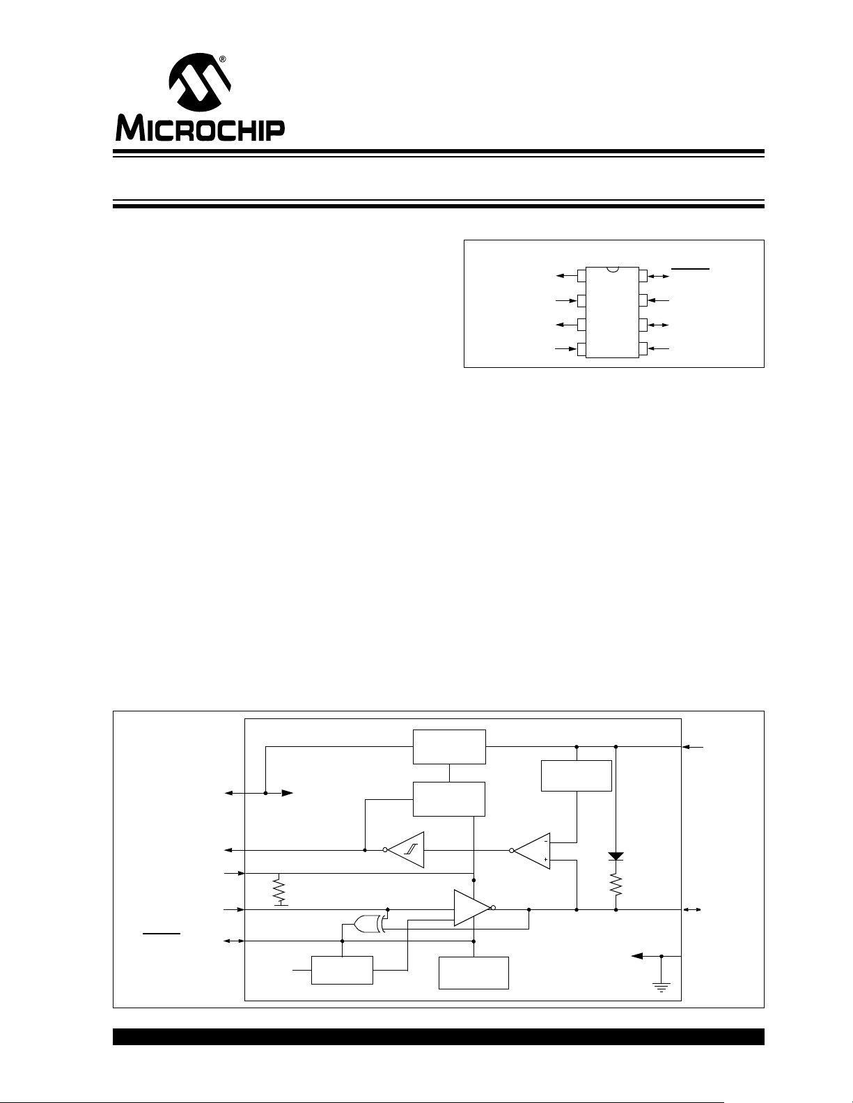
Package Types
PDIP, SOIC, DFN
RXD
CS/WAKE
V
REG
TXD
1
2
3
4
8
7
6
MCP201
5
FAULT/SLPS
VBAT
LIN
SS
V
Block Diagram
Voltage
Regulator
Ratiometric
VREG
RXD
CS/WAKE
TXD
FAULT/SLPS
© 2007 Microchip Technology Inc. DS21730F-page 1
Internal Circuits
POR
Slope
Control
Wake-Up
Logic
OC
Thermal
Protection
Reference
approx.
30 kΩ
Vss
V
BAT
LIN
Page 2

MCP201
NOTES:
DS21730F-page 2 © 2007 Microchip Technology Inc.
Page 3
MCP201
1.0 DEVICE OVERVIEW
The MCP201 provides a physical interface between a
microcontroller and a LIN half-du plex bus. It is i ntended
for automotive and industrial applications with serial
bus speeds up to 20 Kbaud.
The MCP201 provides a half-duplex, bidirectional
communications interface between a microcontroller
and the serial network bus. This device will translate
the CMOS/TTL logic levels to LIN level logic, and vice
versa.
The LIN specification 1.3 requires that the transceiver
of all nodes in the system be connected via the LIN pin,
referenced to ground and with a maximum external
termination resistance of 510Ω from LIN bus to battery
supply. The 510Ω corresponds to 1 Master and 16
Slave nodes.
The MCP201 pro vides a +5V 50 mA regulate d power
output. The regulator uses a LDO design, is shortcircuit-protected and will turn the regulator output off if
it falls below 3.5V. The MCP201 also includes thermal
shutdown protec tion. The regulator has been specifically designed to operate in the automotive environment and will survive reverse battery connections,
+40V load dump transients and double-battery jumps
(see Section 1.6 “Internal Voltage Regulator”).
1.1 Optional External Protection
1.1.1 TRANSIENT VOLTAGE PROTECTION (LOAD DUMP)
An external 27V transient suppressor (TVS) diode,
between V
with the battery supply and the V
tect the device from power transients (see Figure 1-2)
and ESD events. While this protection is optional, it
should be considered as good engineering practice.
BAT and ground, with a 50Ω resistor in series
BAT pin, serves to pro-
1.2 Internal Protection
1.2.1 ESD PROTECTION
For component-level ESD ratings, please refer to the
maximum operation specifications.
1.2.2 GROUND LOSS PROTECTION
The LIN bus specification states that the LIN pin must
transition to the recessive state when ground is
disconnected. Therefore, a loss of ground effectively
forces the LIN line to a hi-impedance level.
1.2.3 THERMAL PROTECTION
The thermal protection circuit monitors the die
temperature and is able to shut down the LIN
transmitter and voltage regulator. Refer to T able 1-1 for
details.
There are three causes for a thermal overload. A
thermal shut down can be triggered by any one, or a
combination of, the following thermal overload
conditions.
• Volt a ge regu lator overload
• LIN bus output overload
• Increase in die temperature due to increase in
environment temperature
Driving the TXD and checking the RXD pin makes it
possible to determi ne whether there is a bus co ntention
(Rx = low, Tx = high) or a thermal overload condition
(Rx = high, Tx = low).
Note: After recovering from a thermal, bus or
voltage regulator overload condition, the
device will be in the Ready1 mode. In order
to go into Operational mode, the CS/
WAKE pin has to be toggled.
1.1.2 REVERSE BATTERY PROTECTION
An external reverse-battery-blocking diode can be
used to provide polarity protection (see Figure 1-2).
This protection is opt ional, but shoul d be considered as
good engineering practice.
TABLE 1-1: SOURCES OF THERMAL OVERLOAD
TXD RXD Comments
L H LIN transmitter shutdown, receiver and voltage regulator active, thermal overload
condition.
H L Regulator shutdown, rece iv er active, bus contention.
Legend: x = Don’t care, L = Low, H = High
Note 1: LIN transceiver overload current on the LIN pin is 200 mA.
2: Voltage regulator overload current on voltage regulator greater than 50mA.
© 2007 Microchip Technology Inc. DS21730F-page 3
(1,2)
Page 4
MCP201
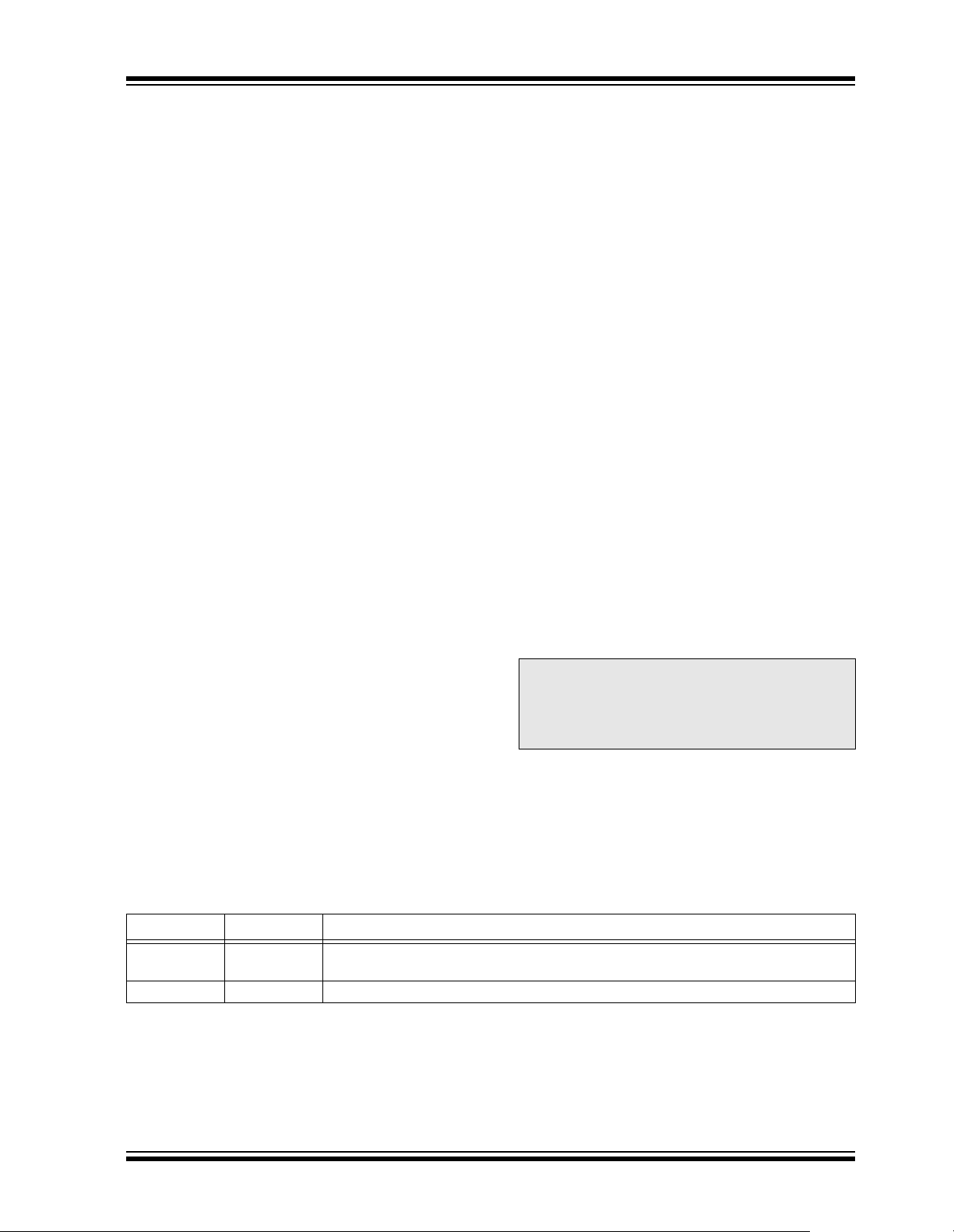
1.3 Modes of Operation
For an overview of all operational modes, please refer
to Table 1-2.
1.3.1 POWER-DOWN MODE
In the Power-down mode, the transmitter and the
voltage regulat or are both off . Only the rec eiver sectio n
and the CS/WAKE pin wake-up circuits are in
operation. This is the lowest power mode.
If any bus activity (e.g., a BREAK character) should
occur during Power-down mode, the device will
immediately enable the voltage regulator. Once the
output has stabilized, the device will enter Ready
mode.
The part will ente r the Operation mod e, if the CS/W AKE
pin should become active-high (‘1’).
1.3.2 READY AND READY1 MODES
There are two states for the Ready mode. The only
difference be tween these states is the transitio n d uring
start-up. The state Ready1 mode ensures that the
transition from Read y to Opera tion mode (once a risin g
edge of CS/WAKE) occurs without disrupting bus
traffic.
Immediately upon entering either Ready1 or Ready
mode, the voltage regulator will turn on and provide
power. The transmitter portion of the circuit is off, with
all other circuit s (in cluding the re ceive r) of the MCP20 1
being fully operational. The LIN pin is kept in a
recessive state.
If a microcontroller is being driven by the voltage
regulator output, it will go through a power-on re set and
initialization sequ enc e. All o ther circuits, other than the
transmitter, are fully operational. The LIN pin is held in
the recessive state.
The device will stay in R eady mode unt il the CS/W AKE
pin transitions high (‘1’). After CS/WAKE is active, the
transmitter is enabled and the device enters Operation
mode.
The device may only enter Power-down mode after
going through the Operation mode step.
At power-on of the V
in either Ready or Ready1 mode, waiting for a
CS/WAKE rising edge.
The MCP201 will stay in either mode for 600 µs as the
regulator powers it s i nternal circuitry and wait s u ntil th e
CS/WAKE pin transitions high. During the 600 µs
delay, the MCP201 will not recognize a CS/WAKE
event. The CS/W AKE transition from low to high should
not occur until after this delay.
• The CS input is edge, no t level, sensitive.
• The CS pin is not monitored until approximately
600 µs after V
• The transistion f rom R eady 1 to Rea dy is made on
the falling edge of CS.
• The transition from Ready mode to Operational
mode is on the rising edge of CS.
BAT supply pin, the component is
REG has stabized.
1.3.3 OPERATION MODE
In this mode, all internal modules are operational.
The MCP201 will go into Power-down mode on the
falling edge of CS/WAKE.
FIGURE 1-1: OPERATIONAL MODES
STATE DIAGRAMS
CS/WAKE = t rue
Operation
Mode
Note: After power-on, CS will not be sampled
Note: While the MCP201 is in shutdown, TXD
Power-down
Mode
CS/WAKE = false
T
L
F
CS/WAKE = t rue
Ready1
Mode
until V
REG has stabized and an additional
Bus Activity
T
L
F
Ready
Mode
CS/WAKE = false
CS/WAKE = true
CS/WAKE = false
POR
Start
600 µs has elapsed. The microcontroller
should toggle CS approx imately 1mS after
RESET to ensure that CS will be recognized.
should not be actively driven high. If TXD
is driven high actively, it may power
internal logic.
1.3.4 DESCRIPTION OF BROWNOUT CONDITIONS
As VBAT decreases VREG is regulated to 5.0 VDC (see
REG in Section 2.2 “DC Specifications”) while VBAT
V
is greater than 5.5 - 6.0 VDC.
BAT decreases further VREG tracks VBAT (VREG =
As V
BAT - (0.5 to 1.0) VDC.
V
The MCP201 monitors V
not fall below V
ifications”), V
BAT increases VREG will continue to track VBAT
As V
SD (see VSD in Section 2.2 “DC Spec-
REG will remain powered.
until VREG reaches 5.0 VDC.
REG falls below VSD, VREG is turned off and the
If V
MCP201 powers itself down.
The MCP201 will remain powered down until V
increases above VON (see VON in Section 2.2 “DC
Specifications”.
REG and as long as V REG does
BAT
DS21730F-page 4 © 2007 Microchip Technology Inc.
Page 5

TABLE 1-2: OVERVIEW OF OPERATIONAL MODES
State Transmitter Voltage Regulator Operation Comments
POR OFF OFF Read CS/WAKE.
If low, then READY.
If high, READY1 mode.
Ready OFF ON If CS/WAKE rising edg e, then
Operation mode.
Ready1 OFF ON If CS/WAKE falling edge,
then READY mode.
Operation ON ON If CS/WAKE falling edge,
then Power down.
Power-down OFF OFF On LIN bus falling, go to
READY mode.
On CS/WAKE rising edg e, go
to Operational mode
Note: After power-on, CS w ill no t be sa mpled until V
microcontroller should toggle CS approximately 1mS after RESET to ensure that CS will be recognized.
REG has sta bized and an addit ion al 600µs has elap sed . The
Sample FAULT/SLPS and
select slope
Bus Off state
Bus Off state
Normal Operation mode
Low-Power mode
MCP201
© 2007 Microchip Technology Inc. DS21730F-page 5
Page 6
MCP201
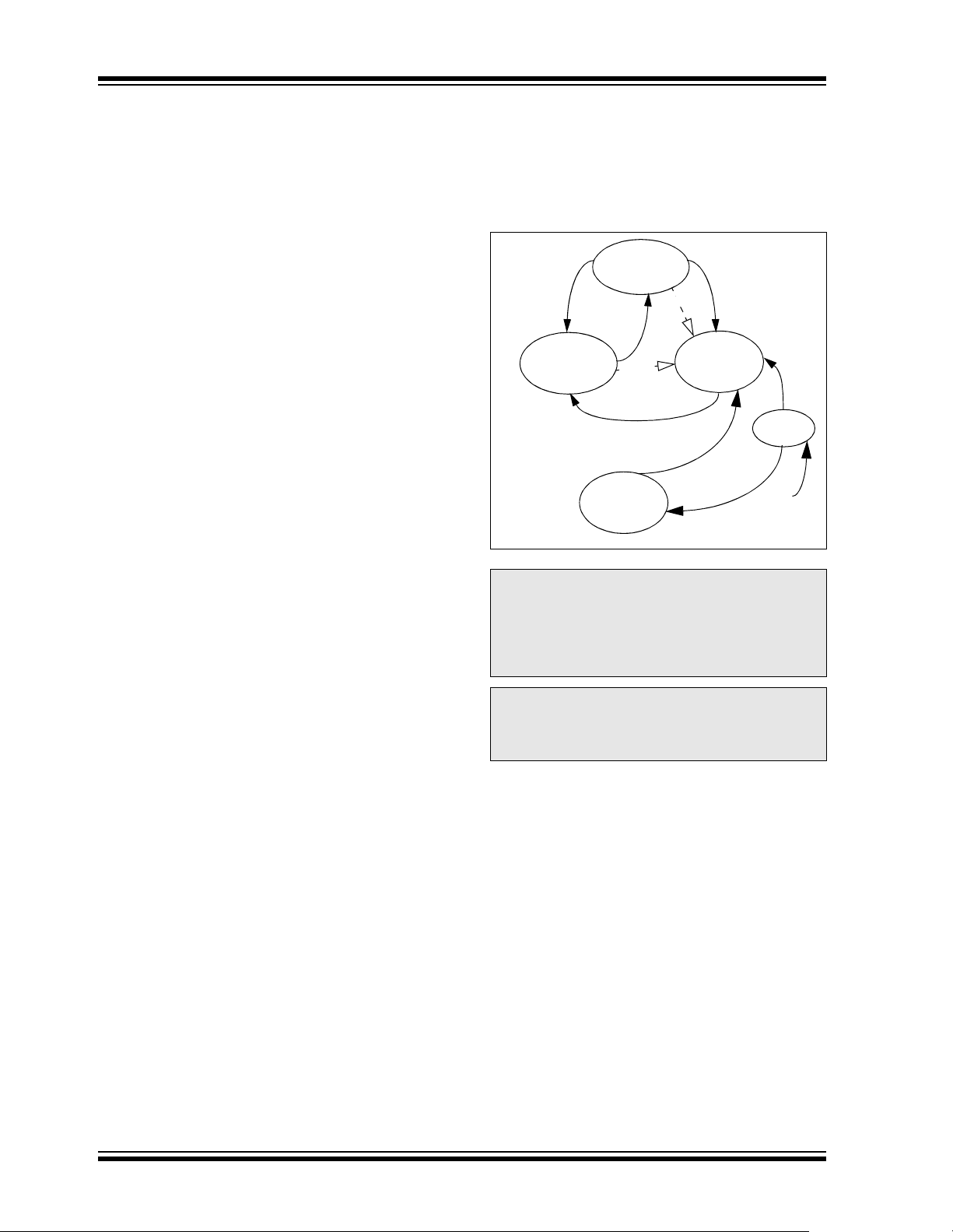
1.4 Typical Applications
FIGURE 1-2: TYPICAL MCP201 APPLICATI ON
+12V
10 kΩ
WAKE-UP
VDD
TXD
®
PIC
MCU
Note 1: The load capacitor, CG, should be a ceramic or t ant alum ra ted for e xtend ed temp erature s and b e in
RXD
I/O
I/O
VSS
the range of 1.0 - 22 µF with an ESR 0.4Ω - 5Ω..
F if the filter capacitor for the external voltage supply.
2: C
3: This diode is only needed if CS/WAKE is connected to 12V supply.
4: Transient suppressor diode. Vclamp L = 40V.
5: These components are for load dump protection.
D1
(3)
CG
+5V
100 kΩ
(1,2)
27V
REG
V
TXD
MCP201
RXD
CS/WAKE
FAULT/SLPS
SS
V
VREG or VSS
+12V
Optional components
Master Node Only
CF
10 uF
VBAT
LIN
1kΩ
(5)
+12V
(4)
D2
24V
Optional components
LIN bus
FIGURE 1-3 : TYPICAL LIN NETWORK C O NF I GUR AT ION
40m
+ Return
LIN bus
BAT
V
DS21730F-page 6 © 2007 Microchip Technology Inc.
1kΩ
LIN bus
MCP201
Master
µC
LIN bus
MCP201
Slave 1
µC
LIN bus
MCP201
Slave 2
µC
LIN bus
MCP201
Slave n <16
µC
Page 7

MCP201
1.5 Pin Descriptions
TABLE 1-3: MCP201 PINOUT OVERVIEW
Devices
8-Pin PDIP/
SOIC/DFN
1 RXD Receive Data Output
2 CS/WAKE Chip Select (TTL-HV
3V
4 TXD Transmit Data Input
5V
6 LIN LIN bus (bidirectional-
7V
8FAULT/SLPS Fault Detect Output,
Legend: TTL = TTL input buffer,
Bond Pad
Name
REG Power Output
SS Ground
BAT Battery
HV = High Voltage (VBAT)
1.5.1 RECEIVE DATA OUTP UT (RX D)
The Receive Data Output pin is a standard CMOS
output and follows the state of the LIN pin.
The LIN receiver monitors the state of the LIN pin and
generates the output signal RXD.
1.5.2 CS/WAKE
Chip Select Input pin. This pi n controls whether the part
goes into READY1 or READY mode at power-up. The
internal pull-down resistor will keep the CS/WAKE pin
low. This is done to ensure that no disruptive data will
be present on the bus while the microcontroller is
executing a Power-on Reset and I/O initialization
sequence. The pin must see a low-to-high transition to
activate the transmitter.
After CS/WAKE transitions to ‘1’, the transmitter is
enabled. If CS/WAKE = ‘0’, the device is in Ready1
mode on power-up or in Low-Power mode. In LowPower mode, the voltage regulator is shut down, the
transmitter driver is disabled and the receiver logic is
enabled.
An external switch (see Figure 1-2) can then wake up
both the transceiver and the microcontroller. An
external-blocking di ode and current-limiti ng resistor are
necessary to protect the microcontroller I/O pin.
Note: On POR, the MCP201 enters Ready or
Ready1 mode (see Figure 1-1). In order to
enter Operational mode, the MCP201 has
to see one rising edge on CS/WAKE
600 µs after the voltage regulator reaches
5V.
Function
Normal Operation
(CMOS output)
input)
(TTL)
HV)
Slope Select Input
1.5.3 POWER OUTPUT (VREG)
Positive Supply Voltage Regulator Output pin.
1.5.4 TRANSMIT DATA INPUT (TXD)
The Transmit Data Input pin has an internal pull-up to
REG. The LIN pi n i s lo w (do m in an t) wh en T XD is l ow,
V
and high (recessive) when TXD is high.
In case the thermal protection detects an over-temperature condition while the signal TXD is low, the
transmitter is shut do wn. The r ecove ry fr om the therma l
shutdown is equal to adequate cooling time.
1.5.5 GROUND (VSS)
Ground pin.
1.5.6 LIN
The bidirectiona l L IN bus Interface pin is the driver unit
for the LIN pin and is contro lle d by the signal T XD. LIN
has an open collector output with a current limitation.
To reduce EMI, the edges during the signal changes
are slope-controlled.
1.5.7 BATTERY (VBAT)
Battery Positive Supply Voltage pin. This pin is also the
input for the internal voltage regulator.
1.5.8 FAULT/SLPS
FAULT Detect Output, Slope Select Input.
This pin is usually in Output mode. Its state is defined
as shown in Table 1-5.
The state of this pin is internally sample d during power-
on of V
(approximately 6 VDC) and V
5.25 VDC, the state of this pin selects which slew rate
profile to apply to the LIN output. It is only during this
time that the pin is used as an input (the output driver
is off during this t ime). The sl ope wil l st ay s electe d unti l
the next V
less of any power-down, wake-up or SLEEP events.
Only a V
FAULT
irrespective of the state of any other pin.
The FAULT
V
the slope selection. This large resistance allows the
FAULT indication function to overdrive the resistor in
normal operation mode.
If the FAULT
ing is selected (dv/dt = 2 V/µs). If FAULT
(‘0’) during this time, the alternate slope-shaping is
selected (dv/dt = 4 V/µs). This mode can be used if a
user desires to run at a faster slope. This mode is not
LIN compliant.
BAT. Once VBAT has reached a stable level,
REG is stable at 4.75 to
BAT power-off/power-on sequence, regard-
BAT rising state will cause a sampling of the
/SLPS pin. The Slope selection will be made
/SLPS pin is connected to either VREG or
SS through a resistor (app roximately 100 kΩ) to make
/SLPS is high (‘1’), the normal slo pe shap-
/SLPS is low
© 2007 Microchip Technology Inc. DS21730F-page 7
Page 8
MCP201
TABLE 1-4: FAULT / SLPS SLOPE
SELECTION DURING POR
/SLPS Slope Shaping
FAULT
HNormal
LAlternate
Note 1: This mode does not conform to LIN bus
specification version 1.3, but might be
(1)
Note: This pin is ‘0’ whenever the internal circuits
have detected a short or thermal excursion
and have disabled the LIN output driver.
Note: Every time TX is togg led , a Fault condition
will occur for the length of time, depending
on the bus load. The Fault time is equal to
the propagation delay.
used for K-line applications.
TABLE 1-5: FAULT
TXD In RXD Out LIN Bus I/O
LHV
/ SLPS TRUTH TABLE
Thermal
Override
BAT OFF L Bus shorted to battery
/ SLPS Out Comments
FAULT
HHVBAT OFF H Bus recessive
L L GND OFF H Bus dominant
H L GND OFF L Bus shorted to ground
xxV
BAT ON L Thermal excursion
Legend: x = don’t care
1.6 Internal Voltage Regulator
6.0V. The device will come up in either READY1 or
READY mode and will have to be transitioned to
The MCP201 has a low drop-out voltage, positive
regulator c apabl e of supp lyin g 5. 00 VDC ±5% at up to
50 mA of load current over the entire operating
temperature range. With a load current of 50 mA, the
minimum input-to-output voltage differential required
for the output to remain in regulation is typically +0.5V
(+1V maximum over the full operating temperature
range). Quiescent current is less than 1.0 mA, with a
full 50 mA load current, when the input-to-output
voltage differential is greater than +2V.
The regulator requires an external output bypass
capacitor for stability. The capacitor should be either a
ceramic or tantalum for stable operation over the
extended temperature range. The compensation
capacitor shou ld ra nge from 1.0 µf – 22 µf and have a
ESR or CSR of 0.4Ω – 5.0Ω. The input capaci tor, C
F, in
Figure 1.4 should be on the order of 8 t o 10 times larger
than the output capacitor, C
G.
Designed for automoti ve applica tions, the reg ulator will
protect itself from rev ers e b atte ry c on nec tio ns, doublebattery jum ps and up to +40V load dump transien ts.
The voltage regulator has both short-circuit and
Operational mode to re-enable data transmission.
In the start phase, V
BAT must be at least 6.0V
(Figure 1-4) to initiate operation during power-up. In
Power-down mode, the VBAT monitor will be turned of f.
The regulator has a thermal shutdown. If the thermal
protection circuit det ects an overtemperature condition
caused by an overcurrent condition (Figure1-6) of the
regulator, it will shut down.
The regulator has an overload current limiting. During
a short-circuit, V
REG is monitored. If VREG is lower than
3.5V , t he regu lator will t urn of f. After a thermal re covery
time, the VREG will be checked again. If there is no
short-circuit (V
REG > 3.5V), the regulator will be
switched back on. The MCP201 will come up in either
READY1 or READY mode and will have to be
transitioned to Operational mode to re-enable data
transmission.
The accuracy of the voltage regulator, when using a
pass transistor, will degrade due to the extra external
components needed. All performance characteristics
should be evaluated on every design.
thermal shutdown protection built-in.
Regarding the correlation between V
BAT, VREG and IDD,
please refer to Figure 1-4 through 1-6. Whe n the input
voltage (V
provide stable regulation, the output V
BAT) drops below the differential neede d to
REG will track the
input down to approxima tely 3.5V, at which po int the
regulator will turn off. This will allow microcontrollers
with internal POR circuits to generate a clean arming of
the Power-on Reset trip poi nt. The MCP201 will then
monitor V
BAT and turn on th e regulator when VBAT is
DS21730F-page 8 © 2007 Microchip Technology Inc.
Page 9
FIGURE 1-4: VOLTAGE REGULATOR OUTPUT ON POWER-ON RESET
VBAT
------------- -
8
6
4
2
V
MCP201
0
VREG
--------------V
5.5
3.5
3
0
(1) (2) (3)
Note 1: Start-up, VBAT < 6.0V, regulator off.
2: VBAT > 6.0V, regulator on.
3: V
BAT ≤ 5.5V, regulator tracks VBAT, regulator will turn
off when V
REG < 3.5V.
t
t
© 2007 Microchip Technology Inc. DS21730F-page 9
Page 10
MCP201
FIGURE 1-5: VOLTAGE REGULATOR OUTPUT ON POWER DIP
VBAT
------------- -
12
8
6
4
3.5
2
V
0
VREG
---------------
5
4
3.5
3
0
Note 1: Voltage regulator on.
2: V
3: VREG < 3. 5V, regulator is of f. If th e volt ag e regu lator shoul d shut
4: V
V
(1) (2) (3)
REG ≤ 5.5V, regulator tracks VBAT until VREG < 3.5V.
off due to V
turn V
REG > 4.0V, voltage regulator tracks VDD, when VREG > 4.0V.
REG falling below 3 .5V, the VBAT must rise to 6.0V to
REG back on.
(4)
t
t
DS21730F-page 10 © 2007 Microchip Technology Inc.
Page 11
MCP201
FIGURE 1-6: VOL TAGE REGULATOR OU TP UT O N OV ER CU RR E N T SI TU AT I O N
IREG
------------mA
50
0
VRE G
-------------- -
6
5
3.5
3
0
Note 1: I
REG less than 50 mA, regulator on.
2: After IREG exceeds IREGmax, voltage regulator output will be reduced
until V
V
(1) (2)
REGoff is reached.
1.7 ICSP™ Considerations
The following should be considered when the MCP201
is connected to pins sup porting in-c ircuit progra mming:
• Power used for programming the microcontroller
should be supplied from the progra mmer , not from
the MCP201
• The MCP201 should be left unpowered
• The voltage on V
maximum output voltage of V
• The TXD pin should not be brought high during
programming
REG should not exceed the
REG
t
t
© 2007 Microchip Technology Inc. DS21730F-page 11
Page 12

MCP201
NOTES:
DS21730F-page 12 © 2007 Microchip Technology Inc.
Page 13

MCP201
2.0 ELECTRICAL CHARACTERISTICS
2.1 Absolute Maximum Ratings†
VIN DC Voltage on Logic pins except CS/WAKE.................................................................................-0.3 to VREG+0.3V
IN DC Voltage on CS/WAKE...............................................................................................................-0.3 to VBAT+0.3V
V
BAT Battery Voltage, non-operating (LIN bus recessive, no regulator load, t < 60s)....................................-0.3 to +40V
V
BAT Battery Voltage, transient (Note 1)........................................................................................................-0.3 to +40V
V
BAT Battery Voltage, continuous ..................................................................................................................-0.3 to +30V
V
LBUS Bus Voltage, continuous.......................................................................................................................-18 to +30V
V
LBUS Bus Voltage, transient (Note 1)............................................................................................................-27 to +40V
V
LBUS Bus Short Circuit Current Limit....................................................................................................................200 mA
I
ESD protection on LIN, V
ESD protection on all other pins (Human Body Model) (Note 2).............................................................................>2 kV
Maximum Junction Temperature.............................................................................................................................150°C
Storage Temperature ..................................................................................................................................-55 to +150°C
Note 1: ISO 7637/1 load dump compliant (t < 500 ms).
2: According to JESD22-A114-B.
BAT (Human Body Model) (Note 2)..................................................................................>4 kV
† NOTICE: Stresse s a bov e th os e l ist ed u nd er “M ax im um R atin gs ” ma y c au se perm an ent dam ag e to the device. This
is a stress rating only and func ti ona l op eration of the device at those or any other conditio ns abo ve those indicated in
the operational li stings of thi s specificati on is not im plied. Expos ure to maximum rat ing cond itions for extend ed periods
may affect device reliability.
© 2007 Microchip Technology Inc. DS21730F-page 13
Page 14

MCP201
2.2 DC Specifications
Electrical Characteristics:
Unless otherwise indicated, all limits are specified for:
DC Specifications
Sym. Parameter Min. Typ. Max. Units Conditions
Power
I
BATQ VBAT Quiescent Operating
Current (voltage regulator
without load and transceiver)
IBAT VBAT Power-down Current
transceiver only
DDQ VREG Quiesce nt Op er at ing
I
Current
VREG VREG maximum output
I
current
Microcontroller Interface
V
IH High-level Input Volta ge
(TXD, FAULT
V
IL Low-level Input Voltage
(TXD, FAULT
I
IHTXD High-level Output Current
/SLPS)
/SLPS)
(TXD)
ILTXD Low-level Output Current
I
(TXD)
V
IHCS/
WAKE
ILCS/
V
WAKE
IHCS/
I
WAKE
I
ILCS/
WAKE
V
OHRXD High-level Output Voltage
High-level Input Voltage
(CS/WAKE)
Low-level Input Voltage
(CS/WAKE)
High-level Input Current
(CS/WAKE)
Low-level Input Current
(CS/WAKE)
(RXD)
OLRXD Low-level Output Voltage
V
(RXD)
Note 1: Internal current limited. 2.0 ms typical recovery time (R
25C. Recovery time highly dependent on ambient temperature, package and thermal resistance).
2: For design guidance only, not tested.
3: This current is at the V
BAT pin.
4: The maximum power dissipation is a function of T
allowable power dissipation at an ambient temperature is P
exceeded, the die temperature will rise above 150°C and the MCP201 will go into thermal shutdown.
VBAT = 6.0V to 18.0V
AMB = -40°C to +125°C
T
LOADREG = 10 µF
C
— 0.45 1.0 mA IVREG = 0 mA, LIN bus pin
recessive, (Note 3)
— 23 50 µA CS/WAKE = High, voltage
regulator disabled
—500 — µA(Note 2)
—— 50 mA(Note 4)
2.0 — V
-0.3 — 0.15 x V
REG + 0.3 V
REG V
-90 — +30 µA Input voltage = 4V
-150 — -10 µA Input voltage = 1V (though
> 50 kΩ internal pull-up)
3.0 — VBAT V Through an external currentlimiting resistor (10 kΩ)
-0.3 — 1.0 V
-10 — +80 µA Input voltage = 4V (though
>100 kΩ internal pull-down)
5 — 30 µA Input voltage = 1V
V
0.8
REG
—— IOH = -4 mA
——0.2 VREG IOL = 4 mA
LBUS = 0Ω, TX = 0.4 VREG, VLBUS = VBAT, TAMB =
JMAX, ΘJA and ambient temperature TA. The maximum
D = (TJMAX - TA)ΘJA. If this dissipation is
DS21730F-page 14 © 2007 Microchip Technology Inc.
Page 15

MCP201
2.2 DC Specifications (Continued)
Electrical Characteristics:
Unless otherwise indicated, all limits are specified for:
DC Specifications
Sym. Parameter Min. Typ. Max. Units Conditions
Bus Interface
VIHLBUS High-level Input Voltage
BUS)
(L
V
ILLBUS Low-level Input Voltage
BUS)
(L
HYS Input Hysteresis 0.05
V
IOL Low-level Output Current
BUS)
(L
O High-level Output Current
I
BUS)
(L
P Pull-up Current on Input
I
(L
BUS)
ISC Short-circuit Current-Limit 50 — 200 mA (Note 1)
VOH High-level Output Vo ltage
(L
BUS)
V
OL Low-level Output Voltage
BUS)
(L
Voltage Regulator
V
REG Output Voltage 4.75 — 5.25 V 0 mA > IOUT > 50 mA,
REG1 Output Voltage 4.4 — 5.25 V 0 mA > IOUT > 50 mA,
V
ΔVREG1 Line Regulation — 1 0 50 mV IOUT = 1 mA, 7.0V < VBAT < 18V
REG2 Load Regulation — 1 0 50 mV 5 mA < IOUT < 50 mA,
ΔV
VN Output Noise Voltage — — 400 µVRMS 1VRMS @ 10 Hz - 100 kHz
SD Shutdown Voltage
V
(monitoring V
V
ON Input Voltage to Turn On
Output (monitoring V
REG)
BAT)
Note 1: Internal current limited. 2.0 ms typical recovery time (R
25C. Recovery time highly dependent on ambient temperature, package and thermal resistance).
2: For design guidance only, not tested.
3: This current is at the V
BAT pin.
4: The maximum power dissipation is a function of T
allowable power dissipation at an ambient temperature is P
exceeded, the die temperature will rise above 150°C and the MCP201 will go into thermal shutdown.
VBAT = 6.0V to 18.0V
AMB = -40°C to +125°C
T
LOADREG = 10 µF
C
0.6 V
BAT — 18 V Recessive state
-8 — 0.4 V
BAT V Dominant state
— 0.1 VBAT VVIH - VIL
V
BAT
40 — 200 mA Output voltage = 0.1 V
BAT = 12V
V
-20 — 20 µA V
BUS ≥ VBAT, VLBUS < 40V
BAT,
-180 — -60 µA Approx. 30 kΩ internal pull-up
@ VIH = 0.7 VBAT
BAT —— V
0.8 V
——0.2 V
BAT V
7.0V < V
6.0V < V
V
BAT < 18V
BAT < 7.0V
BAT = Constant
3.5 — 4.0 V See Figure 1-4
5.5 — 6.0 V
LBUS = 0Ω, TX = 0.4 VREG, VLBUS = VBAT, TAMB =
JMAX, ΘJA and ambient temperature TA. The maximum
D = (TJMAX - TA)ΘJA. If this dissipation is
© 2007 Microchip Technology Inc. DS21730F-page 15
Page 16

MCP201
2.3 AC Specifications
Electrical Characterist ics:
AC Specifications
Symbol Parameter Min Typical Max Units Conditions
Bus Interface
|dV/dt| Slope Rising and Falling Edges 1.0 2.0 3.0 V/
|dV/dt| Slope Rising and Falling edges
ALTERNATE
t
TRANSPD
t
RECPD
t
RECSYM
Propagation Delay of Transmitter — — 6.0 µst
Propagation Delay of Receiver — — 6.0 µs(t
Symmetry of Propagation Delay of
Receiver Rising Edge with Respect
to Falling Edge
t
TRANSSYM
Symmetry of Propagation Delay of
Transmitter Rising Edge with
Respect to Falling Edge
Voltage Regulator
t
BACTVE
Bus Activity to Voltage Regulator
Enabled
t
VEVR
Voltage Regulator Enabled to
Ready
t
R Voltage Regulator Enabled to
VREGPO
Ready after POR
t
CSOR
t
CSPD
t
SHUTDOWN
t
SCREC Short-Circuit Recovery Time — 2.0 — ms Characterized but not
Chip Select to Operation Ready 0 50 200 µs (Note 2)
Chip Select to Power-down 0 — 40 µs (Note 2) No CLOAD
Short-Circuit to Shutdown — 450 — µs Characterized but not
Note 1: The mode does not conform to LIN Bus specification version 1.3.
2: Time depends on external capacitance and load.
3: Internal current limited. 2.0 ms typical recovery time (R
25C. Recovery time highly dependent on ambient temperature, package, and thermal resistance).
Unless otherwise indicated, all limits are specified for:
BAT = 6.0V to 18.0V
V
T
AMB = -40°C to +125°C
µs (40% to 60%), No Load
2.0 4.0 6.0 V/µs(Note 1), No Load
= max
RECPD
RECPDR
-2.0 — 2.0 µst
-2.0 — 2.0 µst
RECSYM
TRANSSYM
(t
TRANSPDF
or t
= max
= max
- t
10 — 40 µs Bus debounce time
—50200µs (Note 2)
——2.5ms(Note 2) CLOAD = 25 nF
tested
tested (Note 3)
LBUS = 0Ω, TX = 0.4 VREG, VLBUS = VBAT, TAMB =
RECPDF
RANSPDR
)
)
TABLE 2-1: MCP201 THERMAL SPECIFICATIONS
Sym Parameter Min Typical Max Units Test Conditions
θ
RECOVERY
θ
SHUTDOWN
t
THERM
Note 1: Internal current limited. 2.0 ms typical recovery time (R
DS21730F-page 16 © 2007 Microchip Technology Inc.
Recovery Temperature
(junction temperature)
Shutdown Temperature
(junction temperature)
Thermal Recovery Time
(after Fault condition removed)
—+135— °C Characterized but not
tested
—+155— °C Characterized but not
tested
— 2.0 — ms Characterized but not
tested (Note 1)
LBUS = 0Ω, TX = 0.4 VREG, VLBUS = VBAT, TAMB =
25C. Recovery time highly dependent on ambient temperature, package, and thermal resistance).
Page 17

2.4 Timing Diagrams and Specifications
FIGURE 2-1: BUS TIMING DIAGRAM
TXD
L
BUS
MCP201
.6 VBAT
.4 VBAT
TTRANSPDF
TRECPDF
RXD
FIGURE 2-2: REGULATO R T IMI NG DIAG RAM ON CS /WAKE SIGNAL
CS/WAKE
TCSOR
VREG
TCSPD
TTRANSPDR
TRECPDR
Regulator Stable
© 2007 Microchip Technology Inc. DS21730F-page 17
Page 18

MCP201
FIGURE 2-3: REGULA TOR TIMI NG DI AGR AM ON BU S ACTI VI TY
Regulator Stable
VREG
TVEVR
TBACTVE
LBUS
.4 VBAT
FIGURE 2-4: POR DIAGRAM
VBAT
VREG
6V
5.0V
tVREGPOR
DS21730F-page 18 © 2007 Microchip Technology Inc.
Page 19

3.0 CHARACTERIZATION GRAPHS
FIGURE 3-1: IDD(mA) vs. VBAT
t
CSPD
(µs) vs. V
700
600
500
400
(µs)
300
CSPD
t
200
100
0
4 6 8 10 12 14 16 18 20
V
BAT
(v)
BAT
(V)
MCP201
t
CSPD
(µs) -40(C)
t
CSPD
(µs) 25(C)
t
CSPD
(µs) 125(C)
dap/jx 3/5/03
30 parts Y1004 B2
© 2007 Microchip Technology Inc. DS21730F-page 19
Page 20

MCP201
FIGURE 3-2: REGULATOR VOLTAGE (V) VS. REGULATOR CURRENT
Regulator Voltage (V) vs. Regulator Current (A)
5.25
5.15
5.05
4.95
4.85
4.75
4.65
4.55
Regulator Voltage (V)
4.45
4.35
4.25
0 102030405060
VREGOUT (V) VBAT 18(V) -40(C)
V
REGOUT (V) VBAT 14.4(V) -40(C)
REGOUT (V) VBAT 8(V) -40(C)
V
REGOUT (V) VBAT 6(V) -40(C)
V
REGOUT (V) VBAT 18(V) 25(C)
V
V
REGOUT (V) VBAT 14.4(V) 25(C)
REGOUT (V) VBAT 8(V) 25(C)
V
V
REGOUT (V) VBAT 6(V) 25(C)
V
REGOUT (V) VBAT 18(V) 125(C)
V
REGOUT (V) VBAT 14.4(V) 125(C)
V
REGOUT (V) VBAT 8(V) 125(C)
REGOUT (V) VBAT 6(V) 125(C)
V
dap/jx
2/28/03
30 parts
Y1004 B2
Regulator Current (mA)
DS21730F-page 20 © 2007 Microchip Technology Inc.
Page 21

FIGURE 3-3: REGULA TOR CHANGE (V) VS. LI NE VOL T AGE CHAN GE
Line Regulation
Regulator Change (V) vs Line Voltage Change (mV)
5
Regulator Change (mV) -40(C) Load = 50(mA)
0
-5
-10
-15
-20
-25
Regulator Change (mV)
-30
-35
-40
0 2 4 6 8 10 12 14
Line Voltage Change (V)
dap/jx
3/3/03
30 parts
Y1004 B2
Regulator Change (mV) -40(C) Load = 25(mA)
Regulator Change (mV) -40(C) Load = 5(mA)
Regulator Change (mV) -40(C) Load = 1(mA)
Regulator Change (mV) 25(C) Load = 50(mA)
Regulator Change (mV) 25(C) Load = 25(mA)
Regulator Change (mV) 25(C) Load = 5(mA)
Regulator Change (mV) 25(C) Load = 1(mA)
Regulator Change (mV) 125(C) Load = 50(mA)
Regulator Change (mV) 125(C) Load = 25(mA)
Regulator Change (mV) 125(C) Load = 5(mA)
Regulator Change (mV) 125(C) Load = 1(mA)
MCP201
© 2007 Microchip Technology Inc. DS21730F-page 21
Page 22

MCP201
g
)
FIGURE 3-4: LOAD REGULATION REGULATOR CHANGE VS. REGULATOR LOAD CHANGE
Load Regulation
Regulator Change (mV) vs. Regulator Load Change (mA)
70
BAT = 18V
BAT = 14.4V
BAT = 8.0V
BAT = 6.0V
BAT = 18V
BAT = 14.4V
BAT = 8.0V
BAT = 6.0V
BAT = 18V
BAT = 14.4V
BAT = 8.0V
BAT = 6.0V
60
50
40
30
Regular Charge (mV)
20
Regulator Change (mV) -40C V
Regulator Change (mV) -40C V
Regulator Change (mV) -40C V
Regulator Change (mV) -40C V
Regulator Change (mV) 25C V
Regulator Change (mV) 25C V
Regulator Change (mV) 25C V
Regulator Change (mV) 25C V
Regulator Change (mV) 125C V
Regulator Change (mV) 125C V
Regulator Change (mV) 125C V
Regulator Change (mV) 125C V
10
0
0 102030405060
ular Load Current Change (mA
Re
dap/jx
3/3/03
30 parts
Y1004 B2
DS21730F-page 22 © 2007 Microchip Technology Inc.
Page 23

FIGURE 3-5: FALLING EDGE NORMAL DV/ D T VS . VBAT
Falling Edge Normal dVdT (V/µs) vs. VBAT(v)
2.40
2.35
2.30
2.25
2.20
2.15
2.10
2.05
2.00
Falling Edge Normal dVdT (V/µs)
1.95
1.90
4 6 8 10 12 14 16 18 20
VBAT(v)
MCP201
Falling Edge Normal
dVdT (V/µs) -40(C)
Falling Edge Normal
dVdT (V/µs) 25(C)
Falling Edge Normal
dVdT (V/µs) 125(C)
dap/jx
3/6/03
30 parts
Y1004 B2
© 2007 Microchip Technology Inc. DS21730F-page 23
Page 24

MCP201
FIGURE 3-6: RISING EDG E NOR MAL DV /D T VS. VBA T
Rising Edge Normal dV/dT (V/µs) vs. VBAT(V)
2.2
2.1
2.0
1.9
1.8
1.7
1.6
1.5
1.4
1.3
1.2
1.1
Rising Edge Normal dV/dT (V/µs)
1.0
0.9
4 6 8 101214161820
VBAT(V)
Rising Edge Normal
dVdT (V/µs) -40(C)
Rising Edge Normal
dVdT (V/µs) 25(C)
Rising Edge Normal
dVdT (V/µs) 125(C)
dap/jx 3/6/03
30 parts Y1004 B2
DS21730F-page 24 © 2007 Microchip Technology Inc.
Page 25

FIGURE 3-7: BUS ACTIVE VS. VBAT
tBACTIVE (µs) vs. VBAT(V)
55
50
45
40
tBACTIVE (µs)
35
30
MCP201
tBACTIVE (µs) -40(C)
tBACTIVE (µs) 25(C)
tBACTIVE (µs) 125(C)
dap/jx 3/6/03
30 parts Y1004 B2
201816141210864
VBAT(V)
© 2007 Microchip Technology Inc. DS21730F-page 25
Page 26

MCP201
FIGURE 3-8: VOLTAGE REGULATOR ACTIVE TIME VS. VBAT
tVEVR (µs) vs. VBAT(V)
10000
1000
tVEVR (µs)
100
10
10
4 6 8 10 12 14 16 18 20
VBAT(v)
tVEVR (µs) -40(C)
tVEVR (µs) 25(C)
tVEVR (µs) 125(C)
dap/jx 3/6/03
30 parts Y1004 B2
DS21730F-page 26 © 2007 Microchip Technology Inc.
Page 27

FIGURE 3-9: CHIP SELECT TO OPERATION READY
tCSOR (µs) vs. VBAT(V)
MCP201
14
13
12
11
10
9
8
tCSOR (µs)
7
6
5
4
tCSOR (µs) -40(C)
tCSOR (µs) 25(C)
tCSOR (µs) 125(C)
dap/jx 3/5/03
30 parts Y1004 B2
201816141210864
VBAT(v)
© 2007 Microchip Technology Inc. DS21730F-page 27
Page 28

MCP201
FIGURE 3-1 0: CHIP SELECT TO POW E R DOW N
tCSPD (µs) vs. VBAT(V)
700
600
500
400
300
tCSPD (µs)
200
100
0
4 6 8 10 12 14 16 18 20
VBAT(v)
tCSPD (µs) -40(C)
tCSPD (µs) 25(C)
tCSPD (µs) 125(C)
dap/jx 3/5/03
30 parts Y1004 B2
DS21730F-page 28 © 2007 Microchip Technology Inc.
Page 29

FIGURE 3-11: PROPAGATION DELAY OF TRANSMITT ER
tTRANSPD (µs) Rising Edge Normal vs. VBAT(V)
MCP201
2.5
2.4
2.3
2.2
2.1
2
1.9
tTRANSPD (µs)
1.8
Rising Edge Normal
1.7
1.6
1.5
4 6 8 10 12 14 16 18 20
tTRANSPD (µs) Rising Edge
Normal -40(C)
tTRANSPD (µs) Rising Edge
Normal 25(C)
tTRANSPD (µs) Rising Edge
Normal 125(C)
dap/jx 3/6/03
30 parts Y1004 B2
VBAT(v)
© 2007 Microchip Technology Inc. DS21730F-page 29
Page 30

MCP201
FIGURE 3-12: PROPAGATION DELAY OF RECEIVER
t
RECPD
(µs) Falling Edge Normal vs. V
BAT
(V)
3.3
3.1
2.9
2.7
2.5
(µs)
2.3
RECPD
t
2.1
Falling Edge Normal
1.9
1.7
1.5
4 6 8 10 12 14 16 18 20
V
BAT
(v)
t
RECPD
(µs) Falling Edge
Normal -40(C)
t
RECPD
(µs) Falling Edge
Normal 25(C)
t
RECPD
(µs) Falling Edge
Normal 125(C)
dap/jx 3/6/03
30 parts Y1004 B2
DS21730F-page 30 © 2007 Microchip Technology Inc.
Page 31

4.0 PACKAGING INFORMATION
4.1 Package Marking Information
MCP201
8-Lead DFN-S
XXXXXXXX
XXXXXXXX
YYWW
NNN
8-Lead PDIP (300 mil)
XXXXXXXX
XXXXXNNN
YYWW
8-Lead SOIC (150 mil)
XXXXXXXX
XXXXYYWW
NNN
Example
MCP201
E/MF
Example:
MCP201
E/P256
Example:
MCP201
E/SN0715
:
0715
256
0715
256
3
e
3
e
3
e
Legend: XX...X Customer-specific information
Y Year code (last digit of calendar year)
YY Year code (last 2 digits of calendar year)
WW Week code (week of January 1 is week ‘01’)
NNN Alphanumeric traceability code
3
e
Pb-free JEDEC designator for Matte Tin (Sn)
* This package is Pb-free. The Pb-free JEDEC designator ( )
can be found on the outer packaging for this package.
Note: In the event the full Microc hip p art numb er cann ot be mark ed on one line, it wil l
be carried over to the next line, thus limiting the number of available
characters for customer-specific information.
© 2007 Microchip Technology Inc. DS21730F-page 31
3
e
Page 32

MCP201
8-Lead Plastic Dual Flat, No Lead Package (MF) – 6x5 mm Body [DFN-S]
P
N
1
2
3
B
UNCH SINGULATED
Note: For the most current package drawings, please see the Microchip Packaging Specification located at
http://www.m icrochip.com/packaging
D
NOTE 1
A
A1
N
1
TOP VIEW
φ
D1
E
E1
EXPOSED
2
A2
A3
b
PAD
2
D2
BOTTOM VIEW
NOTE 2
Units MILLIMETERS
Dimension Limits MIN NOM MAX
Number of Pins N 8
Pitch e 1.27 BSC
Overall Height A – 0.85 1.00
Molded Package Thickness A2 – 0.65 0.80
Standoff A1 0.00 0.01 0.05
Base Thickness A3 0.20 REF
Overall Length D 4.92 BSC
Molded Package Length D1 4.67 BSC
Exposed Pad Length D2 3.85 4.00 4. 15
Overall Width E 5.99 BSC
Molded Package Width E1 5.74 BSC
Exposed Pad Width E2 2.16 2.31 2.46
Contact Width b 0.35 0.40 0.47
Contact Length L 0.50 0.60 0.75
Contact-to-Exposed Pad K 0.20 – –
Model Draft Angle Top φ – – 12°
otes:
. Pin 1 visual index feature may vary, but must be located within the hatched area.
. Package may have one or more exposed tie bars at ends.
. Dimensioning and tolerancing per ASME Y14.5M.
BSC: Basic Dimension. Theoretically exact value shown without tolerances.
REF: Reference Dimension, usually without tolerance, for information purposes only.
DS21730F-page 32 © 2007 Microchip Technology Inc.
e
N
E2
1
L
K
NOTE 1
Microchip Technology Drawing C04-113
Page 33

8-Lead Plastic Dual In-Line (P) – 300 mil Body [PDIP]
N
1
2
3
4
Note: For the most current package drawings, please see the Microchip Packaging Specification located at
http://www.microchip.com/packaging
N
NOTE 1
MCP201
E1
12
A
A1
b1
b
Number of Pins N 8
Pitch e .100 BSC
Top to Seating Plane A – – .210
Molded Package Thickness A2 .115 .130 .195
Base to Seating Plane A1 .015 – –
Shoulder to Shoulder Width E .290 .310 .325
Molded Package Width E1 .240 .250 .280
Overall Length D .348 .365 .400
Tip to Seating Plane L .115 .130 .150
Lead Thickness c .008 .010 .015
Upper Lead Width b1 .040 .060 .070
Lower Lead Width b .014 .018 .022
Overall Row Spacing § eB – – .430
otes:
. Pin 1 visual index feature may vary, but must be located with the hatched area.
. § Significant Characteristic.
. Dimensions D and E1 do not include mold flash or protrusions. Mold flash or protrusions shall not exceed .010" per side.
. Dimensioning and tolerancing per ASME Y14.5M.
BSC: Basic Dimension. Theoretically exact value shown without tolerances.
© 2007 Microchip Technology Inc. DS21730F-page 33
3
D
E
A2
L
e
eB
Units INCHES
Dimension Limits MIN NOM MAX
c
Page 34

MCP201
8-Lead Plastic Small Outline (SN) – Narrow, 3.90 mm Body [SOIC]
N
1
2
3
4
B
Note: For the most current package drawings, please see the Microchip Packaging Specification located at
http://www.microchip.com/packaging
D
N
e
E
E1
NOTE 1
12 3
b
φ
A
A1
A2
Units MILLMETERS
Dimension Limits MIN NOM MAX
Number of Pins N 8
Pitch e 1.27 BSC
Overall Height A – – 1.75
Molded Package Thickness A2 1.25 – –
Standoff
§
A1 0.10 – 0.25
Overall Width E 6.00 BSC
Molded Package Width E1 3.90 BSC
Overall Length D 4.90 BSC
Chamfer (optional) h 0.25 – 0.50
Foot Length L 0.40 – 1.27
Footprint L1 1.04 REF
Foot Angle φ 0° – 8°
Lead Thickness c 0.17 – 0.25
Lead Width b 0.31 – 0.51
Mold Draft Angle Top α 5° – 15°
Mold Draft Angle Bottom β 5° – 15°
otes:
. Pin 1 visual index feature may vary, but must be located within the hatched area.
. § Significant Characteristic.
. Dimens ions D and E1 do not include mold flash or protrusions. Mold flash or protrusions shall not exceed 0.15 mm per side.
. Dimens ioning and tolerancing per ASME Y14.5M.
BSC: Basic Dimension. Theoretically exact value shown without tolerances.
REF: Reference Dimension, usually without tolerance, for information purposes only.
h
L
L1
h
α
c
β
Microchip Technology Drawing C04-057
DS21730F-page 34 © 2007 Microchip Technology Inc.
Page 35

APPENDIX A: REVISION HISTORY
Revision F (January 2007)
This revision includes updates to the packaging
diagrams.
MCP201
© 2007 Microchip Technology Inc. DS21730F-page 35
Page 36

MCP201
NOTES:
DS21730F-page 36 © 2007 Microchip Technology Inc.
Page 37

PRODUCT IDENTIFICATION SYSTEM
To order or obtain information, e.g., on pricing or delivery, refer to the factory or the listed sales office.
MCP201
PART NO. X /XX
Device
Device: MCP2 01: LIN Transceiver with Voltage Regulator
Temperature Range: I = -40°C to +85°C
Package: MF = Dual Flatpack, No-Lead (6x5 mm Body), 8-lead
Range
MCP201T: LIN Transceiver with Voltage Regulator
E = -40°C to +125°C
P = Plastic DIP (300 mil Body), 8-lead
SN = Plastic SOIC (150 mil Body), 8-lead
PackageTemperature
(Tape and Reel)
Examples:
a) MCP201-E/SN: Extended Temperature,
SOIC package.
b) MCP201-E/P: Extended Temperature,
PDIP package.
c) MCP201-I/SN: Industrial Temperature,
SOIC package.
d) MCP201-I/P: Industrial Temperature,
PDIP package.
e) MCP201T-I/SN: Tape and Reel,
Industrial Temperature,
SOIC package.
f) MCP201T-E/SN: Tape and Reel,
Extended Temperature,
SOIC package.
g) MCP201-E/MF: Extended Temperature,
DFN package.
h) MCP201T-E/MF: Tape and Reel,
Extended Temperature,
DFN package.
© 2007 Microchip Technology Inc. DS21730F-page 37
Page 38

MCP201
NOTES:
DS21730F-page 38 © 2007 Microchip Technology Inc.
Page 39

Note the following details of the code protection feature on Microchip devices:
• Microchip products meet the specification contained in their particular Microchip Data Sheet.
• Microchip believes that its family of products is one of the most secure families of its kind on the market today, when used in the
intended manner and under normal conditions.
• There are dishonest and possibly illegal methods used to breach the code protection feature. All of these methods, to our
knowledge, require using the Microchip products in a manner outside the operating specifications contained in Microchip’s Data
Sheets. Most likely, the person doing so is engaged in theft of intellectual property.
• Microchip is willing to work with the customer who is concerned about the integrity of their code.
• Neither Microchip nor any other semiconductor manufacturer can guarantee the security of their code. Code protection does not
mean that we are guaranteeing the product as “unbreakable.”
Code protection is constantly evolving. We at Microchip are com mitted to continuously improving the code protect ion f eatures of our
products. Attempts to break Microchip’s code protection feature may be a violation of the Digit al Mill ennium Copyright Act. If such acts
allow unauthorized access to your software or other copyrighted work, you may have a right to sue for relief under that Act.
Information contained in this publication regarding device
applications and t he lik e is provided only for your convenience
and may be su perseded by updat es . It is y our responsibility to
ensure that your application meets with your specifications.
MICROCHIP MAKES NO REPRESENTATIONS OR
WARRANTIES OF ANY KIND WHETHER EXPRESS OR
IMPLIED, WRITTEN OR ORAL, STATUTORY OR
OTHERWISE, RELATED TO THE INFORMATION,
INCLUDING BUT NOT LIMITED TO ITS CONDITION,
QUALITY, PERFORMANCE, MERCHANTABILITY OR
FITNESS FOR PURPOSE. Microchip disclaims all liability
arising from this information and its use. Use of Microchip
devices in life supp ort and/or safety ap plications is entir ely at
the buyer’s risk, and the buyer agrees to defend, indemnify and
hold harmless M icrochip from any and all dama ges, claims,
suits, or expenses re sulting from such use. No licens es are
conveyed, implicitly or otherwise, under any Microchip
intellectual property rights.
Trademarks
The Microchip name and logo, the Microchip logo, Accuron,
dsPIC, K
EELOQ, microID, MPLAB, PIC, PICmicro, PICSTART,
PRO MATE, PowerSmart, rfPIC, and SmartShunt are
registered trademarks of Microchip Technology Incorporated
in the U.S.A. and other countries.
AmpLab, FilterLab, Migratable Memory, MXDEV, MXLAB,
SEEVAL, SmartSensor and The Embedded Control Solutions
Company are registered trademarks of Microchip Technology
Incorporated in the U.S.A.
Analog-for-the-Digital Age, Application Maestro, CodeGuard,
dsPICDEM, dsPICDEM.net, dsPICworks, ECAN,
ECONOMONITOR, FanSense, FlexROM, fuzzyLAB,
In-Circuit Serial Programming, ICSP, ICEPIC, Linear Active
Thermistor, Mindi, MiWi, MPASM, MPLIB, MPLINK, PIC kit,
PICDEM, PICDEM.net, PICLAB, PICtail, PowerCal,
PowerInfo, PowerMate, Pow e rTool, REAL ICE, rfLAB,
rfPICDEM, Select Mode, Smart Serial, SmartTel, Total
Endurance, UNI/O, WiperLock and ZENA are trademarks of
Microchip Technology I ncorporat ed in the U.S.A. and other
countries.
SQTP is a service mark of Microchip T echnology Incorporated
in the U.S.A.
All other trademarks mentioned herein are property of their
respective companies.
© 2007, Microchip Technology Incorporated, Pr inted in the
U.S.A., All Rights Reserved.
Printed on recycled paper.
Microchip received ISO/TS-16949:2002 certification for its worldwide
headquarters, design and wafer fabrication facilities in Chandler and
Tempe, Arizona, Gresham, Oregon and Mountain View, California. The
Company’s quality system processes and procedures are for its PIC
MCUs and dsPIC DSCs, KEELOQ
EEPROMs, microperipherals, nonvolatile memory and analog
products. In addition, Microchip’s quality system for the design and
manufacture of development systems is ISO 9001:2000 certified.
®
code hopping devices, Serial
© 2007 Microchip Technology Inc. DS21730F-page 39
®
Page 40

WORLDWIDE SALES AND SERVICE
AMERICAS
Corporate Office
2355 West Chandler Blvd.
Chandler, AZ 85224-6199
Tel: 480-792-7200
Fax: 480-792-7277
Techn ical Su pport:
http://support.microchip.com
Web Address:
www.microchip.com
Atlanta
Duluth, GA
Tel: 678-957-9614
Fax: 678-957-1455
Boston
Westborough, MA
Tel: 774-760-0087
Fax: 774-760-0088
Chicago
Itasca, IL
Tel: 630-285-0071
Fax: 630-285-0075
Dallas
Addison, TX
Tel: 972-818-7423
Fax: 972-818-2924
Detroit
Farmington Hills, MI
Tel: 248-538-2250
Fax: 248-538-2260
Kokomo
Kokomo, IN
Tel: 765-864-8360
Fax: 765-864-8387
Los Angeles
Mission Viejo, CA
Tel: 949-462-9523
Fax: 949-462-9608
Santa Clara
Santa Clara, CA
Tel: 408-961-6444
Fax: 408-961-6445
Toronto
Mississauga, Ontario,
Canada
Tel: 905-673-0699
Fax: 905-673-6509
ASIA/PACIFIC
Asia Pacific Office
Suites 3707-14, 37th Floor
Tower 6, The Gateway
Habour City, Kowloon
Hong Kong
Tel: 852-2401-1200
Fax: 852-2401-3431
Australia - Sydney
Tel: 61-2-9868-67 33
Fax: 61-2-9868-6755
China - Beijing
Tel: 86-10-8528-2 100
Fax: 86-10-8528-2104
China - Chengdu
Tel: 86-28-8665-5 511
Fax: 86-28-8665-7889
China - Fuzhou
Tel: 86-591-8750- 3506
Fax: 86-591-8750-3521
China - Hong Kong SAR
Tel: 852-2401-1200
Fax: 852-2401-3431
China - Qingdao
Tel: 86-532-8502- 7355
Fax: 86-532-8502-7205
China - Shanghai
Tel: 86-21-5407-5 533
Fax: 86-21-5407-5066
China - Shenyang
Tel: 86-24-2334-2 829
Fax: 86-24-2334-2393
China - Shenzhen
Tel: 86-755-8203- 2660
Fax: 86-755-8203-1760
China - Shunde
Tel: 86-757-2839-5507
Fax: 86-757-2839-5571
China - Wuhan
Tel: 86-27-5980-5 300
Fax: 86-27-5980-5118
China - Xian
Tel: 86-29-8833-7 250
Fax: 86-29-8833-7256
ASIA/PACIFIC
India - Bangalore
Tel: 91-80-4182-8400
Fax: 91-80-4182-8422
India - New Delhi
Tel: 91-11-4160-8631
Fax: 91-11-4160-8632
India - Pune
Tel: 91-20-2566-1512
Fax: 91-20-2566-1513
Japan - Yokohama
Tel: 81-45-471- 6166
Fax: 81-45-471-6122
Korea - Gumi
Tel: 82-54-473-4301
Fax: 82-54-473-4302
Korea - Seoul
Tel: 82-2-554-7200
Fax: 82-2-558-5932 or
82-2-558-5934
Malaysia - Penang
Tel: 60-4-646-8870
Fax: 60-4-646-5086
Philippines - Manila
Tel: 63-2-634-9065
Fax: 63-2-634-9069
Singapore
Tel: 65-6334-8870
Fax: 65-6334-8850
Taiwan - Hsin Chu
Tel: 886-3-572-9526
Fax: 886-3-572-6459
Taiwan - Kaohsiung
Tel: 886-7-536-4818
Fax: 886-7-536-4803
Taiwan - Taipei
Tel: 886-2-2500-6610
Fax: 886-2-2508-0102
Thailand - Bangkok
Tel: 66-2-694-1351
Fax: 66-2-694-1350
EUROPE
Austria - Wels
Tel: 43-7242-2244-39
Fax: 43-7242-2244-393
Denmark - Copenhagen
Tel: 45-4450-2828
Fax: 45-4485-2829
France - Paris
Tel: 33-1-69-53 -63-20
Fax: 33-1-69-30-90-79
Germany - Munich
Tel: 49-89-627-144-0
Fax: 49-89-627-144-44
Italy - Milan
Tel: 39-0331-742611
Fax: 39-0331-466781
Netherlands - Drunen
Tel: 31-416-690399
Fax: 31-416-690340
Spain - Madrid
Tel: 34-91-708-08-90
Fax: 34-91-708-08-91
UK - Wokingham
Tel: 44-118-921-5869
Fax: 44-118-921-5820
12/08/06
DS21730F-page 40 © 2007 Microchip Technology Inc.
 Loading...