

Page 1

MCP19035
Power Module 8A
Reference Design
User’s Guide
2019 Microchip Technology Inc. DS50002840A
Page 2

Note the following details of the code protection feature on Microchip devices:
YSTEM
CERTIFIE DBYDNV
== ISO/TS16949==
• Microchip products meet the specification contained in their particular Microchip Data Sheet.
• Microchip believes that its family of products is one of the most secure families of its kind on the market today, when used in the
intended manner and under normal conditions.
• There are dishonest and possibly illegal methods used to breach the code protection feature. All of these methods, to our
knowledge, require using the Microchip products in a manner outside the operating specifications contained in Microchip’s Data
Sheets. Most likely, the person doing so is engaged in theft of intellectual property.
• Microchip is willing to work with the customer who is concerned about the integrity of their code.
• Neither Microchip nor any other semiconductor manufacturer can guarantee the security of their code. Code protection does not
mean that we are guaranteeing the product as “unbreakable.”
Code protection is constantly evolving. We at Microchip are committed to continuously improving the code protection features of our
products. Attempts to break Microchip’s code protection feature may be a violation of the Digital Millennium Copyright Act. If such acts
allow unauthorized access to your software or other copyrighted work, you may have a right to sue for relief under that Act.
Information contained in this publication regarding device
applications and the like is provided only for your convenience
and may be superseded by updates. It is your responsibility to
ensure that your application meets with your specifications.
MICROCHIP MAKES NO REPRESENTATIONS OR
WARRANTIES OF ANY KIND WHETHER EXPRESS OR
IMPLIED, WRITTEN OR ORAL, STATUTORY OR
OTHERWISE, RELATED TO THE INFORMATION,
INCLUDING BUT NOT LIMITED TO ITS CONDITION,
QUALITY, PERFORMANCE, MERCHANTABILITY OR
FITNESS FOR PURPOSE. Microchip disclaims all liability
arising from this information and its use. Use of Microchip
devices in life support and/or safety applications is entirely at
the buyer’s risk, and the buyer agrees to defend, indemnify and
hold harmless Microchip from any and all damages, claims,
suits, or expenses resulting from such use. No licenses are
conveyed, implicitly or otherwise, under any Microchip
intellectual property rights unless otherwise stated.
Microchip received ISO/TS-16949:2009 certification for its worldwide
headquarters, design and wafer fabrication facilities in Chandler and
Tempe, Arizona; Gresham, Oregon and design centers in California
and India. The Company’s quality system processes and procedures
are for its PIC
devices, Serial EEPROMs, microperipherals, nonvolatile memory and
analog products. In addition, Microchip’s quality system for the design
and manufacture of development systems is ISO 9001:2000 certified.
®
MCUs and dsPIC® DSCs, KEELOQ
®
code hopping
QUALITYMANAGEMENTS
Trademarks
The Microchip name and logo, the Microchip logo, AnyRate, AVR,
AVR logo, AVR Freaks, BitCloud, chipKIT, chipKIT logo,
CryptoMemory, CryptoRF, dsPIC, FlashFlex, flexPWR, Heldo,
JukeBlox, KeeLoq, Kleer, LANCheck, LINK MD, maXStylus,
maXTouch, MediaLB, megaAVR, MOST, MOST logo, MPLAB,
OptoLyzer, PIC, picoPower, PICSTART, PIC32 logo, Prochip
Designer, QTouch, SAM-BA, SpyNIC, SST, SST Logo,
SuperFlash, tinyAVR, UNI/O, and XMEGA are registered
trademarks of Microchip Technology Incorporated in the U.S.A.
and other countries.
ClockWorks, The Embedded Control Solutions Company,
EtherSynch, Hyper Speed Control, HyperLight Load, IntelliMOS,
mTouch, Precision Edge, and Quiet-Wire are registered
trademarks of Microchip Technology Incorporated in the U.S.A.
Adjacent Key Suppression, AKS, Analog-for-the-Digital Age, Any
Capacitor, AnyIn, AnyOut, BodyCom, CodeGuard,
CryptoAuthentication, CryptoAutomotive, CryptoCompanion,
CryptoController, dsPICDEM, dsPICDEM.net, Dynamic Average
Matching, DAM, ECAN, EtherGREEN, In-Circuit Serial
Programming, ICSP, INICnet, Inter-Chip Connectivity,
JitterBlocker, KleerNet, KleerNet logo, memBrain, Mindi, MiWi,
motorBench, MPASM, MPF, MPLAB Certified logo, MPLIB,
MPLINK, MultiTRAK, NetDetach, Omniscient Code Generation,
PICDEM, PICDEM.net, PICkit, PICtail, PowerSmart, PureSilicon,
QMatrix, REAL ICE, Ripple Blocker, SAM-ICE, Serial Quad I/O,
SMART-I.S., SQI, SuperSwitcher, SuperSwitcher II, Total
Endurance, TSHARC, USBCheck, VariSense, ViewSpan,
WiperLock, Wireless DNA, and ZENA are trademarks of
Microchip Technology Incorporated in the U.S.A. and other
countries.
SQTP is a service mark of Microchip Technology Incorporated in
the U.S.A.
Silicon Storage Technology is a registered trademark of Microchip
Technology Inc. in other countries.
GestIC is a registered trademark of Microchip Technology
Germany II GmbH & Co. KG, a subsidiary of Microchip
Technology Inc., in other countries.
All other trademarks mentioned herein are property of their
respective companies.
© 2019, Microchip Technology Incorporated, All Rights Reserved.
ISBN: 918-1-5224-4099-4
DS50002840A-page 2 2019 Microchip Technology Inc.
Page 3

MCP19035 POWER MODULE
8A REFERENCE DESIGN
USER’S GUIDE
Table of Contents
Preface ........................................................................................................................... 4
Introduction............................................................................................................ 4
Document Layout .................................................................................................. 4
Conventions Used in this Guide ............................................................................ 5
Recommended Reading........................................................................................ 6
The Microchip WebSite ......................................................................................... 6
Customer Support ................................................................................................. 6
Document Revision History ................................................................................... 6
Chapter 1. Product Overview
1.1 Introduction ..................................................................................................... 7
1.2 MCP19035 Overview ..................................................................................... 7
1.3 What is the MCP19035 Power Module 8A Reference Design? ..................... 8
1.4 What the MCP19035 Power Module 8A Reference Design Kit Contains ...... 8
Chapter 2. Installation and Operation
2.1 Introduction ..................................................................................................... 9
2.2 Getting Started ............................................................................................... 9
Appendix A. Schematic and Layouts
A.1 Introduction .................................................................................................. 12
A.2 Board – Schematic ....................................................................................... 13
A.3 Board – Top Silk .......................................................................................... 14
A.4 Board – Top Copper and Silk ....................................................................... 14
A.5 Board – Top Copper .................................................................................... 14
A.6 Board – Bottom Copper ............................................................................... 15
A.7 Board – Bottom Copper and Silk ................................................................. 15
A.8 Board – Bottom Silk ..................................................................................... 15
Appendix B. Bill of Materials (BOM)
Appendix C. Reference Design Waveforms
C.1 Typical Performance Data, Curves and Waveforms .................................... 17
Worldwide Sales and Service .................................................................................... 20
2019 Microchip Technology Inc. DS50002840A-page 3
Page 4

MCP19035 POWER MODULE
8A REFERENCE DESIGN
USER’S GUIDE
Preface
NOTICE TO CUSTOMERS
All documentation becomes dated, and this manual is no exception. Microchip tools and
documentation are constantly evolving to meet customer needs, so some actual dialogs
and/or tool descriptions may differ from those in this document. Please refer to our website
(www.microchip.com) to obtain the latest documentation available.
Documents are identified with a “DS” number. This number is located on the bottom of each
page, in front of the page number. The numbering convention for the DS number is
“DSXXXXXXXXA”, where “XXXXXXXX” is the document number and “A” is the revision level
of the document.
For the most up-to-date information on development tools, see the MPLAB
Select the Help menu, and then Topics, to open a list of available online help files.
INTRODUCTION
This chapter contains general information that will be useful to know before using the
MCP19035 Power Module 8A Reference Design. Items discussed in this chapter
include:
• Document Layout
• Conventions Used in this Guide
• Recommended Reading
• The Microchip WebSite
• Customer Support
• Document Revision History
®
IDE online help.
DOCUMENT LAYOUT
This document describes how to use the MCP19035 Power Module 8A Reference
Design as a development tool to emulate and debug firmware on a target board. The
manual layout is as follows:
• Chapter 1. “Product Overview” – Important information about the MCP19035
Power Module 8A Reference Design.
• Chapter 2. “Installation and Operation” – Includes instructions on installing and
starting the MCP19035 Power Module 8A Reference Design.
• Appendix A. “Schematic and Layouts” – Shows the schematic and layout
diagrams for the MCP19035 Power Module 8A Reference Design.
• Appendix B. “Bill of Materials (BOM)” – Lists the parts used to build the
MCP19035 Power Module 8A Reference Design.
• Appendix C. “Reference Design Waveforms” – Lists the typical performance
data, curves and waveforms.
2019 Microchip Technology Inc. DS50002840A-page 4
Page 5
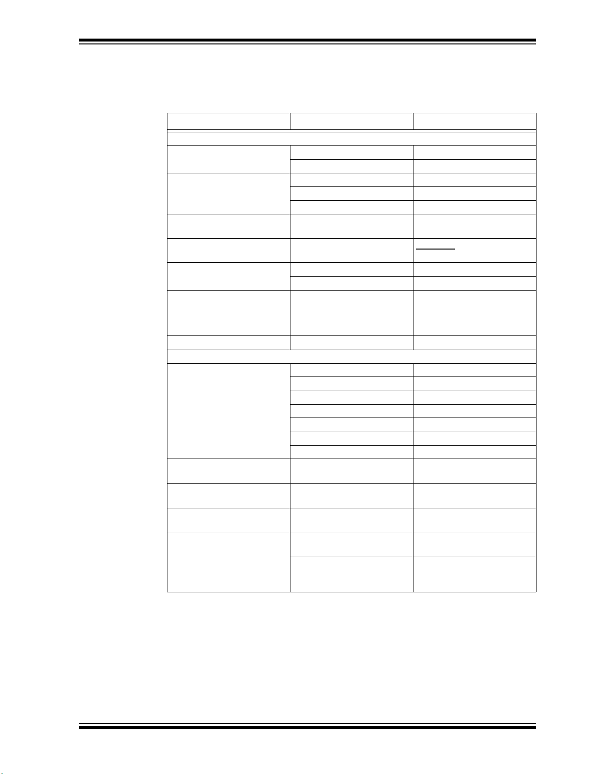
CONVENTIONS USED IN THIS GUIDE
This manual uses the following documentation conventions:
DOCUMENTATION CONVENTIONS
Description Represents Examples
Arial font:
Italic characters Referenced books MPLAB
Initial caps A window the Output window
Quotes A field name in a window or
Underlined, italic text with
right angle bracket
Bold characters A dialog button Click OK
N‘Rnnnn A number in verilog format,
Text in angle brackets < > A key on the keyboard Press <Enter>, <F1>
Courier New font:
Plain Courier New Sample source code #define START
Italic Courier New A variable argument file.o, where file can be
Square brackets [ ] Optional arguments mcc18 [options] file
Curly brackets and pipe
character: { | }
Ellipses... Replaces repeated text var_name [,
Preface
®
IDE User’s Guide
Emphasized text ...is the only compiler...
A dialog the Settings dialog
A menu selection select Enable Programmer
“Save project before build”
dialog
A menu path File>Save
A tab Click the Power tab
4‘b0010, 2‘hF1
where N is the total number of
digits, R is the radix and n is a
digit.
Filenames autoexec.bat
File paths c:\mcc18\h
Keywords _asm, _endasm, static
Command-line options -Opa+, -Opa-
Bit values 0, 1
Constants 0xFF, ‘A’
any valid filename
[options]
Choice of mutually exclusive
arguments; an OR selection
Represents code supplied by
user
errorlevel {0|1}
var_name...]
void main (void)
{ ...
}
2019 Microchip Technology Inc. DS50002840A-page 5
Page 6

RECOMMENDED READING
This user’s guide describes how to use the MCP19035 Power Module 8A Reference
Design. Other useful documents are listed below. The following Microchip documents
are available and recommended as supplemental reference resources:
• MCP19035 Data Sheet – “High-Speed Synchronous Buck Controller”
(DS20002326)
• MCP19035 User’s Guide – “MCP19035 600 kHz High-Voltage Synchronous
Buck Controller Reference Design User’s Guide” (DS50002228)
• MCP19035 Design Analyzer v1.0
THE MICROCHIP WEBSITE
Microchip provides online support via our website at www.microchip.com. This website
is used as a means to make files and information easily available to customers.
Accessible by using your favorite Internet browser, the website contains the following
information:
• Product Support – Data sheets and errata, application notes and sample
programs, design resources, user’s guides and hardware support documents,
latest software releases and archived software
• General Technical Support – Frequently Asked Questions (FAQs), technical
support requests, online discussion groups, Microchip consultant program
member listing
• Business of Microchip – Product selector and ordering guides, latest Microchip
press releases, listing of seminars and events, listings of Microchip sales offices,
distributors and factory representatives
Preface
CUSTOMER SUPPORT
Users of Microchip products can receive assistance through several channels:
• Distributor or Representative
• Local Sales Office
• Field Application Engineer (FAE)
• Technical Support
Customers should contact their distributor, representative or field application engineer
(FAE) for support. Local sales offices are also available to help customers. A listing of
sales offices and locations is included in the back of this document.
Technical support is available through the website at:
http://www.microchip.com/support.
DOCUMENT REVISION HISTORY
Revision A (January 2019)
• Initial release of this document
2019 Microchip Technology Inc. DS50002840A-page 6
Page 7

Chapter 1. Product Overview
C
IN
C
OUT
MCP19035
HDRV
LDRV
PHASE
BOOT
+VCC
C
BOOT
C
VCC
+V
OUT
SHDN
V
IN
PWRGD
COMP
FB
+VIN
ON
OFF
1.1 INTRODUCTION
This chapter provides an overview of the MCP19035 Power Module 8A Reference
Design and covers the following topics:
• MCP19035 Overview
• What is the MCP19035 Power Module 8A Reference Design?
• What the MCP19035 Power Module 8A Reference Design Kit Contains
1.2 MCP19035 OVERVIEW
The MCP19035 is a highly-featured, highly-integrated, synchronous buck controller in
a space-saving 10-pin DFN 3x3 package that operates from input voltage sources up
to 30V. Integrated features include high and low-side MOSFET drivers, fixed-frequency
voltage mode control, internal oscillator and reference voltage generator, overcurrent
protection circuit for both sides, Power Good (PG) circuit and overtemperature protection. A minimal number of external components are necessary to develop a complete,
high-performance synchronous buck converter power supply.
The MCP19035 Synchronous Buck Controller is intended to be used for applications
requiring medium-to-high output currents (up to 20A) and input voltages up to 30V.
Typical applications include: medium currents Point-of-Load converters, FPGA/DSP
power supplies, USB power ports, digital Set-Top boxes, industrial 24V rails converters,
high-power LED drivers.
The internal high-current linear voltage regulator (LDO) allows low-current loads (ex.
®
PIC
microcontrollers) to be powered directly from this controller without any additional
components.
MCP19035 POWER MODULE
8A REFERENCE DESIGN
USER’S GUIDE
FIGURE 1-1: Typical Application.
2019 Microchip Technology Inc. DS50002840A-page 7
Page 8

1.3 WHAT IS THE MCP19035 POWER MODULE 8A REFERENCE DESIGN?
The MCP19035 Power Module 8A Reference Design is a compact, highly efficient,
step-down voltage circuit that will convert the input voltage rail (typically 12V) to 5V regulated output voltage. The maximum output current for this step-down converter is 8A.
The board demonstrates the capabilities of the MCP19035 600 kHz Synchronous Buck
Converter Controller in a typical high-voltage input step-down application. The
MCP19035 Power Module 8A Reference Design can be modified to support output
voltages from 3.3V to 5.5V by changing a single resistor.
1.4 WHAT THE MCP19035 POWER MODULE 8A REFERENCE DESIGN KIT CONTAINS
The MCP19035 Power Module 8A Reference Design includes the following items:
• MCP19035 Power Module 8A Reference Design (ADM00987)
• Important Information Sheet
2019 Microchip Technology Inc. DS50002840A-page 8
Page 9

Chapter 2. Installation and Operation
2.1 INTRODUCTION
The MCP19035 Power Module 8A Reference Design was developed to provide a
compact, low-cost and highly efficient step-down conversion for low to medium output
currents.
The key features of this board include:
• Input Voltage Range: 6V to 18V
• Output Voltage: 5V (can be adjusted by changing one resistor between 3.3V and
5V)
• Maximum Output Current: 8A
• 95% Typical Efficiency at 5V/8A Output and 12V Input
• 600 kHz Fixed Switching Frequency
• Over-Current Protection for High and Low-Side MOSFETs
• Shutdown Input for Placing the Converter in Low-Power Standby Mode
• Under Voltage Lockout (UVLO) with 4.5V and 3.9V (typical) Thresholds
MCP19035 POWER MODULE
8A REFERENCE DESIGN
USER’S GUIDE
2.2 GETTING STARTED
The MCP19035 Power Module 8A Reference Design is fully assembled and tested to
evaluate and demonstrate the MCP19035 capabilities.
2.2.1 Necessary Instruments and Tools
• Adjustable DC Power Supply with 0V-30V/5ADC range output capability
• Electronic Load with at least 8A current capability and load stepping capability
• Digital Oscilloscope with a minimum bandwidth of 50 MHz
• Digital Voltmeter/Ammeter
• Wires for connections; these wires must sustain high currents, 8A for the connection between adjustable DC Power Supply and board, 8A for the connection
between board and the Electronic Load
2.2.2 Setup Procedure
To power-up the MCP19035 Power Module 8A Reference Design, the following steps
must be completed:
1. Connect the Electronic Load to the J1 connector of the reference design; the
positive (+) and negative (-) connector pins are the 2, 3 and 4 pins, for positive,
respectively 5, 6,10 pins, for negative, off the J1 connector.
2. Connect the Adjustable DC Power Supply to the J1 connector of the reference
design; the positive (+) and negative (-) connector pins are the 7 and 8 pins, for
positive, respectively 5, 6,10 pins, for negative, off the J1 connector.
3. The DC voltage supplied by the Adjustable DC Power Supply must be 12V.
2019 Microchip Technology Inc. DS50002840A-page 9
Page 10

Installation and Operation
2.2.3 Board Testing
The typical application is shown in Figure 2-1 and the 3D view of the board with the J1
connector pins numbered is shown in Figure 2-2. For more details, see Appendix
A. “Schematic and Layouts”.
The user can connect various instruments at the listed pins of the J1 connector to evaluate the parameters of the converter. The typical performance data, curves and waveforms are presented in Section C.1 “Typical Performance Data, Curves and
Waveforms”.
The user also has two ways to connect the R4 to the circuit. First is to mount the resistor
on the silk footprint on the board, and the second is to connect the R4 to the pins.
FIGURE 2-1: Schematic.
FIGURE 2-2: 3D View of the Board.
2019 Microchip Technology Inc. DS50002840A-page 10
Page 11

Installation and Operation
R
4
R3V
REF
V
OUTVREF
–
------------------------------- -=
Where:
V
REF
= 0.6V
R
3
= 20 kΩ
2.2.4 Adjusting the Output Voltage
The output voltage can be modified by changing the value of R4 from the feedback
divider. The output voltage is set according to Equation 2-1.
EQUATION 2-1:
Do not modify the value of the R3 resistor (20 kΩ), as this will affect the loop compensation of the system.
Some parameters, such as the efficiency, the overcurrent protection thresholds and the
input and output voltage ripples can be affected by the modification of the output voltage. Do not exceed 6V for the output voltage or permanent damage of the board can
occur.
Ta bl e 2 -1 shows the standard values of the R4 resistor for a few usual output voltages.
TABLE 2-1: OUTPUT VOLTAGE VS. R4 VALUE
V
OUT
3.3 4.42 4.3
5 2.74 2.7
R4 (kΩ)
calculated
R4 (kΩ)
E24 standard
2.2.5 Testing Procedure
In the testing procedure, measurements are made on a testing board to help get better
results, as the parameters are at 12V voltage on input and 8A current on output.
2019 Microchip Technology Inc. DS50002840A-page 11
Page 12

Appendix A. Schematic and Layouts
A.1 INTRODUCTION
This appendix contains the following schematics and layouts for the MCP19035 Power
Module 8A Reference Design - ADM00995:
• Board – Schematic
• Board – Top Silk
• Board – Top Copper and Silk
• Board – Top Copper
• Board – Bottom Copper
• Board – Bottom Copper and Silk
• Board – Bottom Silk
MCP19035 POWER MODULE
8A REFERENCE DESIGN
USER’S GUIDE
2019 Microchip Technology Inc. DS50002840A-page 12
Page 13

DS50002840A-page 13 2019 Microchip Technology Inc.
*1'
*1'
*1'
*1' *1'
*1'
*1' *1'
0.33uF
16V
&
100k
1%
5
2.7k
1%
YES
5
20k
5%
5
750R
1%
5
9LQ
9RXW
6+'1
2XWSXW7ULP
3+$6(
MCP19035-BAABE/MF
6+'1
)%
&203
9,1
3:5*'
9&&
/'59
%227
3+$6(
+'59
(3
8
*1'
+'59
/'59
MCP87055T
1,2,3
5,6,7,8
4
MCP87055T
1,2,3
5,6,7,8
4
6+'1
2XWSXW7ULP
*1'
47pF
50V
&
5600pF
50V
&
&203
100k
1%
5
9&&
9&&
3:5*'
73
73
9LQ 99
,RXWPD[ $
5IE
5IE 9UHI[5IE N
9RXW9UHI
5 9RXW
N 9
N 9
5IE
2XWSXW7ULP
9RXW
([WHUQDO7ULP5HVLVWRU
9RXW9
'13
GHWHUPLQHG
E\5IE
HDR-2 Male 2x5
-
9RXW
9LQ
4.7uF
35V
&
4.7uF
35V
&
2.2uH
XAL7070-222MEC
/
2.7k
0402 1%
5
680pF
50V
0402
&
22uF
10V
1206
&
22uF
10V
1206
&
1uF
25V
0603
&
1uF
25V
0603
&
5IE
A.2 BOARD – SCHEMATIC
MCP19035 Power Module 8A Reference Design User’s Guide
Page 14

A.3 BOARD – TOP SILK
A.4 BOARD – TOP COPPER AND SILK
Schematic and Layouts
A.5 BOARD – TOP COPPER
2019 Microchip Technology Inc. DS50002840A-page 14
Page 15

A.6 BOARD – BOTTOM COPPER
A.7 BOARD – BOTTOM COPPER AND SILK
Schematic and Layouts
A.8 BOARD – BOTTOM SILK
2019 Microchip Technology Inc. DS50002840A-page 15
Page 16

MCP19035 POWER MODULE
8A REFERENCE DESIGN
USER’S GUIDE
Appendix B. Bill of Materials (BOM)
TABLE B-1: BILL OF MATERIALS (BOM)
Qty. Reference Description Manufacturer Part Number
2 C1, C2 Capacitor Ceramic, 4.7 µF, 35V, 10%, X7R,
SMD, 0805
1 C3 Capacitor Ceramic, 5600 pF, 50V, 10%, X7R,
SMD, 0402
1 C4 Capacitor Ceramic, 0.33 µF, 16V, 10%, X7R,
SMD, 0603
1 C5 Capacitor Ceramic, 47 pF, 50V, 5%, NP0,
SMD, 0402
2 C6, C9 Capacitor Ceramic, 1 µF, 25V, 10%, X7R,
SMD, 0603, AEC-Q200
2 C7, C8 Capacitor Ceramic, 22 µF, 10V, 10%, X7R,
SMD, 1206, AEC-Q200
1 C10 Capacitor Ceramic, 680 pF, 50V, 10%, X7R,
SMD, 0402
1 J1 Connector Header-2, Male, 2x5, Gold, TH, RASamtec, Inc. TMM-105-01-L-D-RA
TDK Corporation C2012X7R1V475K125AE
Samsung ElectroMechanics America, Inc
Murata Electronics® GRM188R71C334KA01D
Murata Electronics® GRM1555C1H470JA01D
Samsung ElectroMechanics America, Inc.
Taiyo Yuden Co., Ltd. LMJ316BB7226KLHT
Wurth Elektronik 885012205060
CL05B562KB5NNNC
CL10B105KA8VPNC
1 L1 Inductor 2.2 µH, 17.8A, 20%, SMD,
L7.5W7.2D7
1 PCB1 Printed Circuit Board Microchip Technology
2 Q1, Q2 Microchip Analog MOSFET N-CH, 25V, 60A,
MCP87055T-U/LC PDFN-8
2 R1, R6 Resistor, TKF, 100k, 1%, 1/10W, SMD, 0402 Panasonic
1 R2 Resistor, TKF, 2.7k, 1%, 1/10W, SMD, 0402 Panasonic
1 R3 Resistor, TKF, 20k, 5%, 1/10W, SMD, 0402 Panasonic® - ECG ERJ-2GEJ203X
0 R4 Do Not Populate – Resistor, TKF, 2.7k, 1%,
1/10W, SMD, 0402
1 R5 Resistor, TKF, 750R, 1/10W, 1%, SMD, 0402 Panasonic® - ECG ERJ-2RKF7500X
1 U1 Microchip Analog PWM Controller, 600 kHz,
MCP19035-BAABE/MF DFN-10
Note 1: The components listed in this Bill of Materials are representative of the PCB assembly. The released BOM
used in manufacturing uses all RoHS-compliant components.
Coilcraft XAL7070-222MEC
04-10880-R1
Inc.
Microchip Technology
Inc.
®
- ECG ERJ-2RKF1003X
®
- ECG ERJ-2RKF2701X
Panasonic
Microchip Technology
Inc.
®
- ECG ERJ-2RKF2701X
MCP87055T-U/LC
MCP19035-BAABE/MF
2019 Microchip Technology Inc. DS50002840A-page 16
Page 17

MCP19035 POWER MODULE
(IILFLHQF\
,
287
$
(II9
(IIY
(II9
(II9
(II9
(II 9
8A REFERENCE DESIGN
USER’S GUIDE
Appendix C. Reference Design Waveforms
C.1 TYPICAL PERFORMANCE DATA, CURVES AND WAVEFORMS
This chapter shows some of the typical performance parameters and curves of the
MCP19035 Power Module 8A Reference Design.
TABLE C-1: CONVERTER PARAMETERS
Parameter Value Comments
Input Voltage Range (V) 6 - 18
Output Voltage (V) 5 ±1.5% Tolerance
Maximum Output Current (A) 8 Steady state output current
Output Voltage Ripple (mV) < 25 V
Input Voltage Ripple (mV) < 300 VIN = 12V, I
Output Voltage Overshoot during
Step Load (mV)
Switching Frequency (kHz) 550 - 650 Typical 600 kHz
< 200 Step Load 0A to 8A
= 12V, I
IN
OUT
OUT
= 8A
= 8A
FIGURE C-1: Efficiency vs. I
OUT
(A).
2019 Microchip Technology Inc. DS50002840A-page 17
Page 18

MCP19035 Power Module 8A Reference Design User’s Guide
9
287
9
,
287
$
FIGURE C-2: Load Regulation (VIN=12V).
FIGURE C-3: Output Voltage Ripple/Noise (V
BW = 20MHz).
2019 Microchip Technology Inc. DS50002840A-page 18
=12V, I
IN
OUT
=8A,
Page 19

MCP19035 Power Module 8A Reference Design User’s Guide
FIGURE C-4: Input Voltage Ripple/Noise (VIN=12V, I
FIGURE C-5: Step Load (VIN=12V, I
= 0A to 8A).
OUT
= 8A, BW = 20MHz).
OUT
2019 Microchip Technology Inc. DS50002840A-page 19
Page 20

Worldwide Sales and Service
AMERICAS
Corporate Office
2355 West Chandler Blvd.
Chandler, AZ 85224-6199
Tel: 480-792-7200
Fax: 480-792-7277
Technical Support:
http://www.microchip.com/
support
Web Address:
www.microchip.com
Atlanta
Duluth, GA
Tel: 678-957-9614
Fax: 678-957-1455
Austin, TX
Tel: 512-257-3370
Boston
Westborough, MA
Tel: 774-760-0087
Fax: 774-760-0088
Chicago
Itasca, IL
Tel: 630-285-0071
Fax: 630-285-0075
Dallas
Addison, TX
Tel: 972-818-7423
Fax: 972-818-2924
Detroit
Novi, MI
Tel: 248-848-4000
Houston, TX
Tel: 281-894-5983
Indianapolis
Noblesville, IN
Tel: 317-773-8323
Fax: 317-773-5453
Tel: 317-536-2380
Los Angeles
Mission Viejo, CA
Tel: 949-462-9523
Fax: 949-462-9608
Tel: 951-273-7800
Raleigh, NC
Tel: 919-844-7510
New York, NY
Tel: 631-435-6000
San Jose, CA
Tel: 408-735-9110
Tel: 408-436-4270
Canada - Toronto
Tel: 905-695-1980
Fax: 905-695-2078
ASIA/PACIFIC
Australia - Sydney
Tel: 61-2-9868-6733
China - Beijing
Tel: 86-10-8569-7000
China - Chengdu
Tel: 86-28-8665-5511
China - Chongqing
Tel: 86-23-8980-9588
China - Dongguan
Tel: 86-769-8702-9880
China - Guangzhou
Tel: 86-20-8755-8029
China - Hangzhou
Tel: 86-571-8792-8115
China - Hong Kong SAR
Tel: 852-2943-5100
China - Nanjing
Tel: 86-25-8473-2460
China - Qingdao
Tel: 86-532-8502-7355
China - Shanghai
Tel: 86-21-3326-8000
China - Shenyang
Tel: 86-24-2334-2829
China - Shenzhen
Tel: 86-755-8864-2200
China - Suzhou
Tel: 86-186-6233-1526
China - Wuhan
Tel: 86-27-5980-5300
China - Xian
Tel: 86-29-8833-7252
China - Xiamen
Tel: 86-592-2388138
China - Zhuhai
Tel: 86-756-3210040
ASIA/PACIFIC
India - Bangalore
Tel: 91-80-3090-4444
India - New Delhi
Tel: 91-11-4160-8631
India - Pune
Tel: 91-20-4121-0141
Japan - Osaka
Tel: 81-6-6152-7160
Japan - Tokyo
Tel: 81-3-6880- 3770
Korea - Daegu
Tel: 82-53-744-4301
Korea - Seoul
Tel: 82-2-554-7200
Malaysia - Kuala Lumpur
Tel: 60-3-7651-7906
Malaysia - Penang
Tel: 60-4-227-8870
Philippines - Manila
Tel: 63-2-634-9065
Singapore
Tel: 65-6334-8870
Taiwan - Hsin Chu
Tel: 886-3-577-8366
Taiwan - Kaohsiung
Tel: 886-7-213-7830
Taiwan - Taipei
Tel: 886-2-2508-8600
Thailand - Bangkok
Tel: 66-2-694-1351
Vietnam - Ho Chi Minh
Tel: 84-28-5448-2100
EUROPE
Austria - Wels
Tel: 43-7242-2244-39
Fax: 43-7242-2244-393
Denmark - Copenhagen
Tel: 45-4450-2828
Fax: 45-4485-2829
Finland - Espoo
Tel: 358-9-4520-820
France - Paris
Tel: 33-1-69-53-63-20
Fax: 33-1-69-30-90-79
Germany - Garching
Tel: 49-8931-9700
Germany - Haan
Tel: 49-2129-3766400
Germany - Heilbronn
Tel: 49-7131-67-3636
Germany - Karlsruhe
Tel: 49-721-625370
Germany - Munich
Tel: 49-89-627-144-0
Fax: 49-89-627-144-44
Germany - Rosenheim
Tel: 49-8031-354-560
Israel - Ra’anana
Tel: 972-9-744-7705
Italy - Milan
Tel: 39-0331-742611
Fax: 39-0331-466781
Italy - Padova
Tel: 39-049-7625286
Netherlands - Drunen
Tel: 31-416-690399
Fax: 31-416-690340
Norway - Trondheim
Tel: 47-7288-4388
Poland - Warsaw
Tel: 48-22-3325737
Romania - Bucharest
Tel: 40-21-407-87-50
Spain - Madrid
Tel: 34-91-708-08-90
Fax: 34-91-708-08-91
Sweden - Gothenberg
Tel: 46-31-704-60-40
Sweden - Stockholm
Tel: 46-8-5090-4654
UK - Wokingham
Tel: 44-118-921-5800
Fax: 44-118-921-5820
2019 Microchip Technology Inc. DS50002840A-page 20
08/15/18
 Loading...