


MCP1825/MCP1825S
500 mA, Low Voltage, Low Quiescent Current LDO Regulator
Features
• 500 mA Output Current Capability
• Input Operating Voltage Range: 2.1V to 6.0V
• Adjustable Output Voltage Range: 0.8V to 5.0V
(MCP1825 only)
• Standard Fixed Output Voltages:
- 0.8V, 1.2V, 1.8V, 2.5V, 3.0V, 3.3V, 5.0V
• Other Fixed Output Voltage Options Available
Upon Request
• Low Dropout Voltage: 210 mV Typical at 500 mA
• Typical Output Voltage Tolerance: 0.5%
• Stable with 1.0 µF Ceramic Output Capacitor
• Fast response to Load Transients
• Low Supply Current: 120 µA (typ)
• Low Shutdown Supply Current: 0.1 µA (typ)
(MCP1825 only)
• Fixed Delay on Power Good Output
(MCP1825 only)
• Short Circuit Current Limiting and
Overtemperature Protection
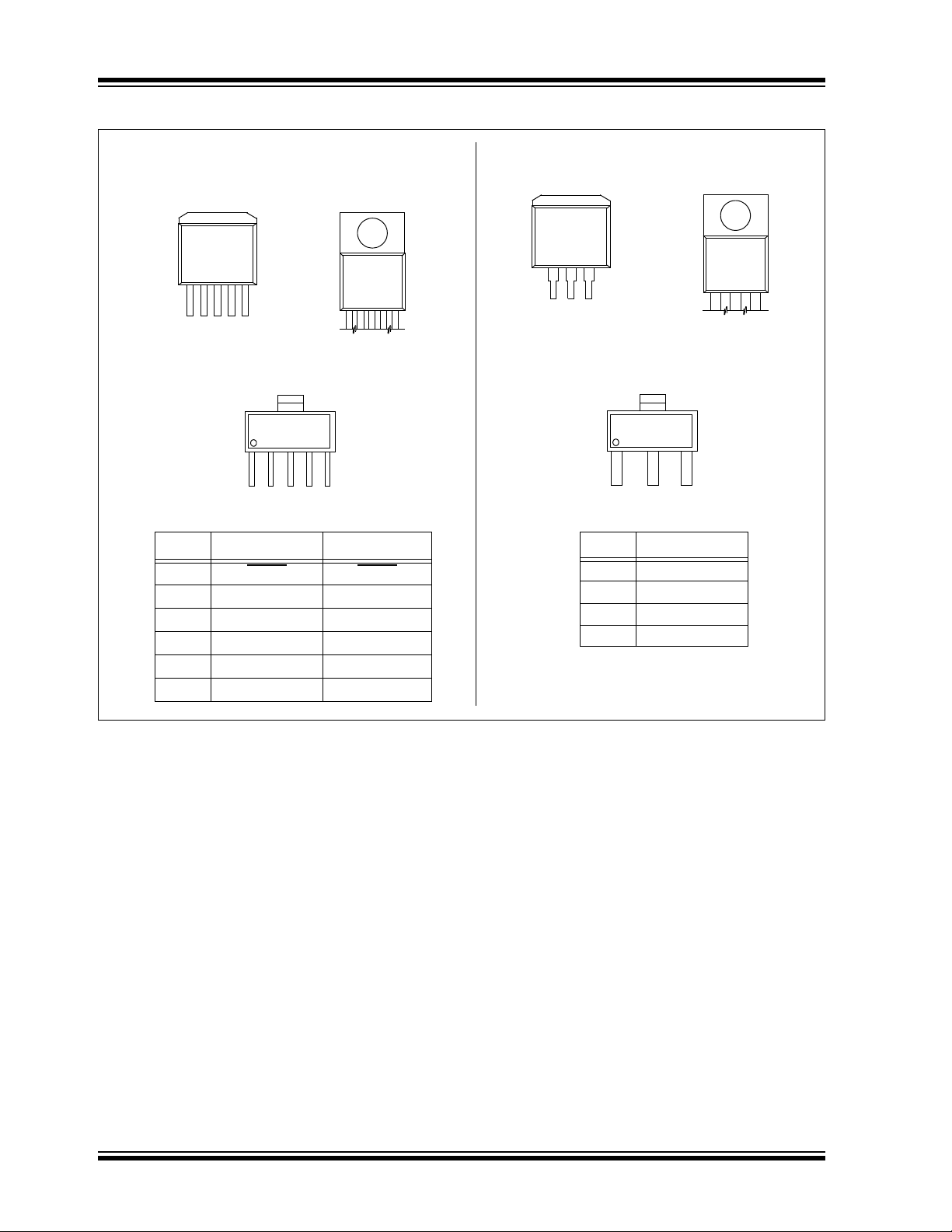
• TO-263-5 (DDPAK-5), TO-220-5, SOT-223-5
Package Options (MCP1825).
• TO-263-3 (DDPAK-3), TO-220-3, SOT-223-3
Package Options (MCP1825S).
Applications
• High-Speed Driver Chipset Power
• Networking Backplane Cards
• Notebook Computers
• Network Interface Cards
• Palmtop Computers
• 2.5V to 1.XV Regulators
Description
The MCP1825/MCP1825S is a 500 mA Low Dropout
(LDO) linear regulator that provides high current and
low output voltages. The MCP1825 comes in a fixed or
adjustable output voltage version, with an output
voltage range of 0.8V to 5.0V. The 500 mA output
current capability, combined with the low output voltage
capability, make the MCP1825 a good choice for new
sub-1.8V output voltage LDO applications that have
high current demands. The MCP1825S is a 3-pin fixed
voltage version.
The MCP1825/MCP1825S is stable using ceramic
output capacitors that inherently provide lower output
noise and reduce the size and cost of the entire
regulator solution. Only 1 µF of output capacitance is
needed to stabilize the LDO.
Using CMOS construction, the quiescent current
consumed by the MCP1825/MCP1825S is typically
less than 120 µA over the entire input voltage range,
making it attractive for portable computing applications
that demand high output current. The MCP1825
versions have a Shutdown (S
down, the quiescent current is reduced to less than
0.1 µA.
On the MCP1825 fixed output versions, the scaleddown output voltage is internally monitored and a
power good (PWRGD) output is provided when the
output is within 92% of regulation (typical). The
PWRGD delay is internally fixed at 110 µs (typical).
The overtemperature and short circuit current-limiting
provide additional protection for the LDO during system
fault conditions.
HDN) pin. When shut
© 2007 Microchip Technology Inc. DS22056A-page 1
MCP1825/MCP1825S
MCP1825
1234
5
6
SOT-223-5
Pin Fixed Adjustable
1 SHDN
SHDN
2V
IN
V
IN
3 GND (TAB) GND (TAB)
4V
OUT
V
OUT
5 PWRGD ADJ
6 GND (TAB) GND (TAB)
1
2
3
SOT-223-3
4
MCP1825S
Pin
1V
IN
2 GND (TAB)
3V
OUT
4 GND (TAB)
Fixed/Adjustable
DDPAK-3DDPAK-5 TO-220-3TO-220-5
12345
12345
123
123
Package Types
DS22056A-page 2 © 2007 Microchip Technology Inc.
Typical Applications
MCP1825 Adjustable Output Voltage
MCP1825 Fixed Output Voltage
V
OUT
= 1.8V @ 500 mA
VIN = 2.3V to 2.8V
On
Off
1µF
100 kΩ
4.7 µF
C
1
C
2
R
1
SHDN
V
IN
GND
V
OUT
PWRGD
20 kΩ
R
2
V
OUT
= 1.2V @ 500 mA
VIN = 2.1V to 2.8V
On
Off
1µF
40 kΩ
4.7 µF
C
1
C
2
R
1
SHDN
V
IN
GND
V
OUT
V
ADJ
1
1
MCP1825/MCP1825S
© 2007 Microchip Technology Inc. DS22056A-page 3
MCP1825/MCP1825S
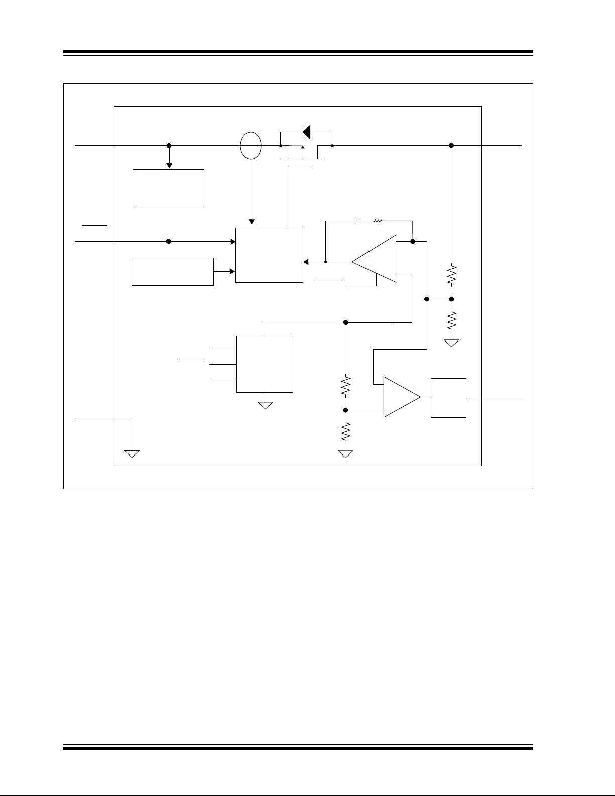
EA
+
–
V
OUT
PMOS
R
f
C
f
I
SNS
Overtemperature
V
REF
Comp
92% of V
REF
T
DELAY
V
IN
Driver w/limit
and SHDN
GND
Soft-Start
ADJ/SENSE
Undervoltage
Lock Out
V
IN
Reference
SHDN
SHDN
SHDN
Sensing
(UVLO)
Functional Block Diagram - Adjustable Output
DS22056A-page 4 © 2007 Microchip Technology Inc.
Functional Block Diagram - Fixed Output (3-Pin)
EA
+
–
V
OUT
PMOS
R
f
C
f
I
SNS
Overtemperature
V
REF
Comp
92% of V
REF
T
DELAY
V
IN
Driver w/limit
and SHDN
GND
Soft-Start
Sense
Undervoltage
Lock Out
V
IN
Reference
SHDN
SHDN
SHDN
Sensing
(UVLO)
MCP1825/MCP1825S
© 2007 Microchip Technology Inc. DS22056A-page 5
MCP1825/MCP1825S
EA
+
–
V
OUT
PMOS
R
f
C
f
I
SNS
Overtemperature
V
REF
Comp
92% of V
REF
T
DELAY
V
IN
Driver w/limit
and SHDN
GND
Soft-Start
Sense
Undervoltage
Lock Out
V
IN
Reference
SHDN
SHDN
SHDN
Sensing
(UVLO)
PWRGD
Functional Block Diagram - Fixed Output (5-Pin)
DS22056A-page 6 © 2007 Microchip Technology Inc.
MCP1825/MCP1825S
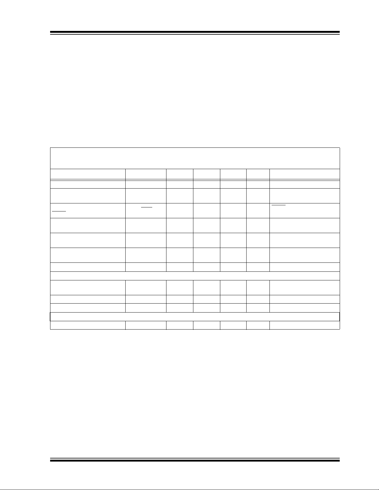
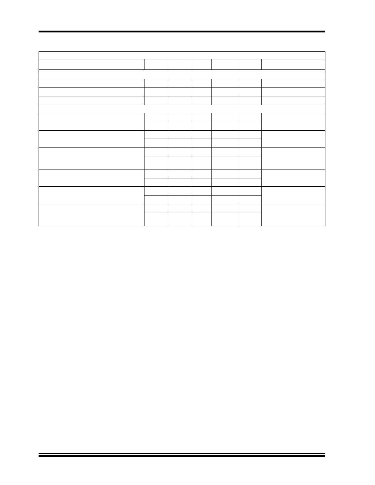
1.0 ELECTRICAL
CHARACTERISTICS
† Notice: Stresses above those listed under “Maximum Rat-
ings” may cause permanent damage to the device. This is a
stress rating only and functional operation of the device at
those or any other conditions above those indicated in the
Absolute Maximum Ratings †
VIN....................................................................................6.5V
Maximum Voltage on Any Pin.. (GND – 0.3V) to (V
DD
+ 0.3)V
operational listings of this specification is not implied. Exposure to maximum rating conditions for extended periods may
affect device reliability.
Maximum Power Dissipation......... Internally-Limited (Note 6)
Output Short Circuit Duration ................................ Continuous
Storage temperature .....................................-65°C to +150°C
Maximum Junction Temperature, T
ESD protection on all pins (HBM/MM)
........................... +150°C
J
........... ≥ 4kV; ≥ 300V
AC/DC CHARACTERISTICS
Electrical Specifications: Unless otherwise noted, VIN = V
I
= 1 mA, CIN = C
OUT
Boldface type applies for junction temperatures, T
= 4.7 µF (X7R Ceramic), TA = +25°C.
OUT
J
OUT(MAX)
(Note 7) of -40°C to +125°C
Parameters Sym Min Typ Max Units Conditions
Input Operating Voltage V
Input Quiescent Current I
Input Quiescent Current for
SHDN
Mode
I
Maximum Output Current I
Line Regulation ΔV
(V
OUT
Load Regulation ΔV
Output Short Circuit Current I
OUT/VOUT
OUT_SC
IN
q
SHDN
OUT
OUT
x ΔVIN)
/
2.1 6.0 V Note 1
— 120 220 µA IL = 0 mA, V
—0.1 3 µA SHDN = GND
500 ——mAV
— ±0.05 ±0.16 %/V (Note 1) ≤ V
-1.0 ±0.5 1.0 %I
—1.2—AR
Adjust Pin Characteristics (Adjustable Output Only)
Adjust Pin Reference Voltage V
Adjust Pin Leakage Current I
Adjust Temperature Coefficient TCV
ADJ
ADJ
OUT
0.402 0.410 0.418 VVIN = 2.1V to VIN=6.0V,
-10 ±0.01 +10 nA VIN = 6.0V, V
— 40 — ppm/°C Note 3
Fixed-Output Characteristics (Fixed Output Only)
Voltage Regulation V
Note 1: The minimum V
must meet two conditions: VIN ≥ 2.1V and VIN ≥ V
IN
OUT
VR - 2.5% VR ±0.5% VR + 2.5% V Note 2
2: VR is the nominal regulator output voltage for the fixed cases. VR = 1.2V, 1.8V, etc. VR is the desired set point output
voltage for the adjustable cases. V
3: TCV
= (V
OUT
OUT-HIGH
temperature range. V
– V
OUT-LOW
OUT-LOW
R
= V
((R1/R2)+1). Figure 4-1.
ADJ *
) *106 / (VR * ΔTemperature). V
is the lowest voltage measured over the temperature range.
4: Load regulation is measured at a constant junction temperature using low duty-cycle pulse testing. Load regulation is
tested over a load range from 1 mA to the maximum specified output current.
5: Dropout voltage is defined as the input-to-output voltage differential at which the output voltage drops 2% below its
nominal value that was measured with an input voltage of V
6: The maximum allowable power dissipation is a function of ambient temperature, the maximum allowable junction
temperature and the thermal resistance from junction to air. (i.e., T
dissipation will cause the device operating junction temperature to exceed the maximum +150°C rating. Sustained
junction temperatures above 150°C can impact device reliability.
7: The junction temperature is approximated by soaking the device under test at an ambient temperature equal to the
desired junction temperature. The test time is small enough such that the rise in the junction temperature over the
ambient temperature is not significant.
+ V
DROPOUT(MAX)
= V
IN
, Note 1, VR = 1.8V for Adjustable Output,
5.0V
= 2.1V to 6.0V
IN
V
= 0.8V to 5.0V, Note 1
R
= 1 mA to 500 mA,
OUT
(Note 4)
<0.1Ω, Peak Current
LOAD
I
= 1 mA
OUT
OUT(MAX)
OUT-HIGH
OUT(MAX)
, TJ, θJA). Exceeding the maximum allowable power
A
+ V
DROPOUT(MAX).
is the highest voltage measured over the
+ V
DROPOUT(MAX)
.
= 0.8V to
OUT
≤ 6V
IN
ADJ
=0Vto6V
© 2007 Microchip Technology Inc. DS22056A-page 7
MCP1825/MCP1825S
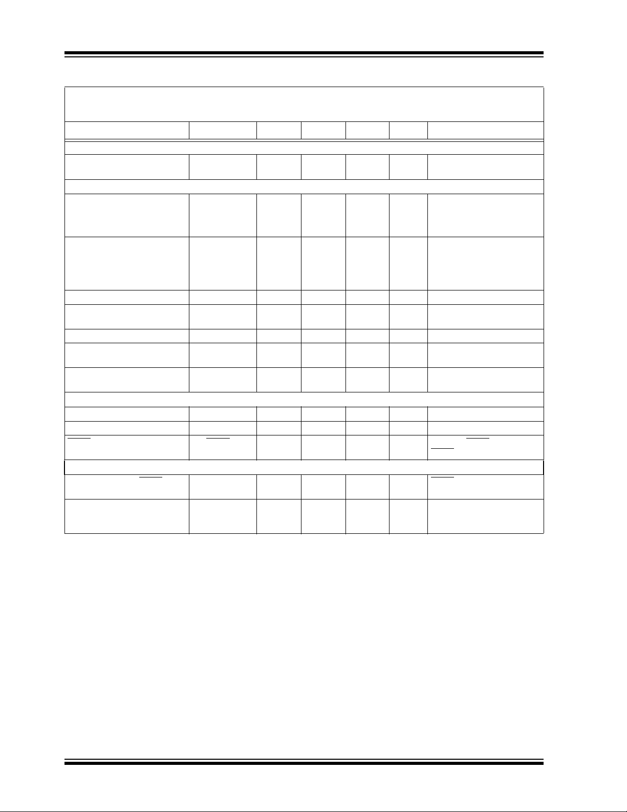
AC/DC CHARACTERISTICS (CONTINUED)
Electrical Specifications: Unless otherwise noted, VIN = V
I
= 1 mA, CIN = C
OUT
Boldface type applies for junction temperatures, T
= 4.7 µF (X7R Ceramic), TA = +25°C.
OUT
J
OUT(MAX)
(Note 7) of -40°C to +125°C
Parameters Sym Min Typ Max Units Conditions
Dropout Characteristics
Dropout Voltage V
DROPOUT
— 210 350 mV Note 5, I
Power Good Characteristics
PWRGD Input Voltage Operating Range
PWRGD Threshold Voltage
(Referenced to V
OUT
)
V
PWRGD_VIN
V
PWRGD_TH
1.0 — 6.0 V TA = +25°C
1.2 — 6.0 T
89 92 95 V
90 92 94 V
PWRGD Threshold Hysteresis V
PWRGD Output Voltage Low V
PWRGD Leakage P
PWRGD_HYS
PWRGD_L
WRGD_LK
PWRGD Time Delay T
Detect Threshold to PWRGD
Active Time Delay
T
VDET-PWRGD
PG
1.0 2.0 3.0 %V
—0.20.4 VI
—1—nAV
— 110 — µs Rising Edge
— 200 — µs V
Shutdown Input
Logic High Input V
Logic Low Input V
Input Leakage Current SHDN
SHDN
SHDN-HIGH
SHDN-LOW
ILK
45 ——%VINVIN = 2.1V to 6.0V
——15 %VINVIN = 2.1V to 6.0V
-0.1 ±0.001 +0.1 µA VIN=6V, SHDN =VIN,
AC Performance
Output Delay From SHDN
Output Noise e
Note 1: The minimum V
must meet two conditions: VIN ≥ 2.1V and VIN ≥ V
IN
T
OR
N
— 100 — µs SHDN = GND to VIN,
—2.0—µV/√Hz I
2: VR is the nominal regulator output voltage for the fixed cases. VR = 1.2V, 1.8V, etc. VR is the desired set point output
voltage for the adjustable cases. V
3: TCV
= (V
OUT
OUT-HIGH
temperature range. V
OUT-LOW
– V
OUT-LOW
R
= V
((R1/R2)+1). Figure 4-1.
ADJ *
) *106 / (VR * ΔTemperature). V
is the lowest voltage measured over the temperature range.
4: Load regulation is measured at a constant junction temperature using low duty-cycle pulse testing. Load regulation is
tested over a load range from 1 mA to the maximum specified output current.
5: Dropout voltage is defined as the input-to-output voltage differential at which the output voltage drops 2% below its
nominal value that was measured with an input voltage of V
6: The maximum allowable power dissipation is a function of ambient temperature, the maximum allowable junction
temperature and the thermal resistance from junction to air. (i.e., T
dissipation will cause the device operating junction temperature to exceed the maximum +150°C rating. Sustained
junction temperatures above 150°C can impact device reliability.
7: The junction temperature is approximated by soaking the device under test at an ambient temperature equal to the
desired junction temperature. The test time is small enough such that the rise in the junction temperature over the
ambient temperature is not significant.
+ V
DROPOUT(MAX)
= V
IN
, Note 1, VR = 1.8V for Adjustable Output,
OUT
=2.1V
IN(MIN)
= -40°C to +125°C
A
< 2.1V, I
IN
< 2.5V Fixed,
OUT
= Adj.
OUT
>= 2.5V Fixed
OUT
PWRGD SINK
%V
OUT
OUT
V
For V
Falling Edge
V
ADJ = 0V
= VIN = 6.0V
PWRGD
R
to V
SHDN
V
C
V
OUT(MAX)
OUT-HIGH
OUT(MAX)
, TJ, θJA). Exceeding the maximum allowable power
A
+ V
DROPOUT(MAX).
is the highest voltage measured over the
+ V
DROPOUT(MAX)
= 10 kΩ
PULLUP
= V
OUT
PWRGD_TH
PWRGD_TH
= GND
= GND to 95% VR
OUT
= 200 mA, f = 1 kHz,
OUT
= 10 µF (X7R Ceramic),
OUT
= 2.5V
OUT
.
= 500 mA,
= 100 µA
SINK
= 1.2 mA,
+ 20 mV
- 20 mV
DS22056A-page 8 © 2007 Microchip Technology Inc.
MCP1825/MCP1825S
AC/DC CHARACTERISTICS (CONTINUED)
Electrical Specifications: Unless otherwise noted, VIN = V
I
= 1 mA, CIN = C
OUT
Boldface type applies for junction temperatures, T
= 4.7 µF (X7R Ceramic), TA = +25°C.
OUT
J
OUT(MAX)
(Note 7) of -40°C to +125°C
Parameters Sym Min Typ Max Units Conditions
Power Supply Ripple Rejection
PSRR — 60 — dB f = 100 Hz, C
Ratio
Thermal Shutdown Temperature T
Thermal Shutdown Hysteresis ΔT
Note 1: The minimum V
must meet two conditions: VIN ≥ 2.1V and VIN ≥ V
IN
SD
SD
— 150 — °C I
—10—°CI
2: VR is the nominal regulator output voltage for the fixed cases. VR = 1.2V, 1.8V, etc. VR is the desired set point output
voltage for the adjustable cases. V
3: TCV
= (V
OUT
OUT-HIGH
temperature range. V
– V
OUT-LOW
OUT-LOW
R
= V
((R1/R2)+1). Figure 4-1.
ADJ *
) *106 / (VR * ΔTemperature). V
is the lowest voltage measured over the temperature range.
4: Load regulation is measured at a constant junction temperature using low duty-cycle pulse testing. Load regulation is
tested over a load range from 1 mA to the maximum specified output current.
5: Dropout voltage is defined as the input-to-output voltage differential at which the output voltage drops 2% below its
nominal value that was measured with an input voltage of V
6: The maximum allowable power dissipation is a function of ambient temperature, the maximum allowable junction
temperature and the thermal resistance from junction to air. (i.e., T
dissipation will cause the device operating junction temperature to exceed the maximum +150°C rating. Sustained
junction temperatures above 150°C can impact device reliability.
7: The junction temperature is approximated by soaking the device under test at an ambient temperature equal to the
desired junction temperature. The test time is small enough such that the rise in the junction temperature over the
ambient temperature is not significant.
+ V
DROPOUT(MAX)
= V
IN
, Note 1, VR = 1.8V for Adjustable Output,
I
= 100 µA,
OUT
V
= 100 mV pk-pk,
INAC
C
= 0 µF
IN
= 100 µA, V
OUT
V
= 2.8V
IN
= 100 µA, V
OUT
V
= 2.8V
IN
OUT(MAX)
OUT-HIGH
OUT(MAX)
, TJ, θJA). Exceeding the maximum allowable power
A
+ V
DROPOUT(MAX).
is the highest voltage measured over the
+ V
DROPOUT(MAX)
.
OUT
= 4.7 µF,
= 1.8V,
OUT
= 1.8V,
OUT
© 2007 Microchip Technology Inc. DS22056A-page 9
MCP1825/MCP1825S
TEMPERATURE SPECIFICATIONS
Parameters Sym Min Typ Max Units Conditions
Temperature Ranges
Operating Junction Temperature Range T
Maximum Junction Temperature T
Storage Temperature Range T
Thermal Package Resistances
Thermal Resistance, 3LD DDPAK θ
Thermal Resistance, 3LD TO-220 θ
Thermal Resistance, 3LD SOT-223 θ
Thermal Resistance, 5LD DDPAK θ
Thermal Resistance, 5LD TO-220 θ
Thermal Resistance, 5LD SOT-223 θ
J
J
A
JA
θ
JC
JA
θ
JC
JA
θ
JC
JA
θ
JC
JA
θ
JC
JA
θ
JC
-40 — +125 °C Steady State
— — +150 °C Transient
-65 — +150 °C
— 31.4 — °C/W 4-Layer JC51 Standard
—3.0 —
Board
— 29.4 — °C/W 4-Layer JC51 Standard
—2.0 —
Board
— 62 — °C/W EIA/JEDEC JESD51-
— 15.0 —
751-7
4 Layer Board
— 31.2 — °C/W 4-Layer JC51 Standard
—3.0 —
Board
— 29.3 — °C/W 4-Layer JC51 Standard
—2.0 —
Board
— 62 — °C/W EIA/JEDEC JESD51-
— 15.0 —
751-7
4 Layer Board
DS22056A-page 10 © 2007 Microchip Technology Inc.
MCP1825/MCP1825S
90
100
110
120
130
140
23456
Input Voltage (V)
Quiescent Current (μA)
130°C
-45°C
25°C
90°C
V
OUT
= 1.2V Adj
I
OUT
= 0 mA
0°C
100
110
120
130
140
150
160
170
180
190
200
0 100 200 300 400 500 600
Load Current (mA)
Ground Current (μA)
VIN=3.3V
V
OUT
= 1.2V Adj
VIN=5.0V
VIN=2.5V
90
100
110
120
130
140
150
160
170
-45 -20 5 30 55 80 105 130
Temperature (°C)
Quiescent Current (μA)
VIN=6.0V
VIN=3.0V
VIN=4.0V
V
OUT
= 1.2V Adj
I
OUT
= 0 mA
VIN=5.0V
VIN=2.1V
0.00
0.01
0.02
0.03
0.04
0.05
0.06
0.07
0.08
0.09
0.10
-45 -20 5 30 55 80 105 130
Temperature (°C)
Line Regulation (%/V)
V
OUT
V
IN
I
OUT
= 1 mA
I
OUT
=500 mA
I
OUT
= 50 mA
I
OUT
=100 mA
I
OUT
=100 mA
-0.15
-0.10
-0.05
0.00
0.05
0.10
0.15
0.20
-45-20 5 305580105130
Temperature (°C)
Load Regulation (%)
I
OUT
= 1.0 mA to 1500 mA
V
OUT
= 5.0V
V
OUT
= 3.3V
V
OUT
= 0.8V
V
OUT
= 1.8V
0.4070
0.4075
0.4080
0.4085
0.4090
0.4095
0.4100
0.4105
0.4110
-45 -20 5 30 55 80 105 130
Temperature (°C)
Adjust Pin Voltage (V)
V
OUT
= 1.8V
I
OUT
= 1.0 mA
VIN = 2.3V
VIN = 6.0V
VIN = 4.0V
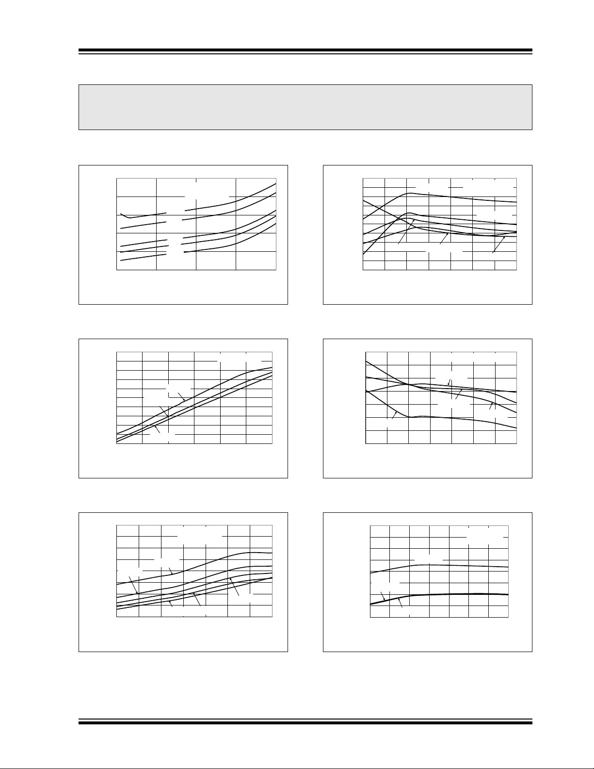
2.0 TYPICAL PERFORMANCE CURVES
Note: The graphs and tables provided following this note are a statistical summary based on a limited number of
samples and are provided for informational purposes only. The performance characteristics listed herein
are not tested or guaranteed. In some graphs or tables, the data presented may be outside the specified
operating range (e.g., outside specified power supply range) and therefore outside the warranted range.
Note: Unless otherwise indicated, C
Temperature = +25°C, V
IN
= V
OUT
= 4.7 µF Ceramic (X7R), CIN = 4.7 µF Ceramic (X7R), I
OUT
+ 0.5V, Fixed output.
OUT
= 1 mA,
= 1.2V adj
= 2.1V to 6.0V
FIGURE 2-1: Quiescent Current vs. Input Voltage (Adjustable Version).
FIGURE 2-2: Ground Current vs. Load Current (Adjustable Version).
FIGURE 2-4: Line Regulation vs. Temperature (Adjustable Version).
FIGURE 2-5: Load Regulation vs. Temperature (Adjustable Version).
FIGURE 2-3: Quiescent Current vs. Junction Temperature (Adjustable Version).
© 2007 Microchip Technology Inc. DS22056A-page 11
FIGURE 2-6: Adjust Pin Voltage vs. Temperature (Adjustable Version).

MCP1825/MCP1825S
0.00
0.05
0.10
0.15
0.20
0.25
0.30
0 50 100 150 200 250 300 350 400 450 500
Load Current (mA)
Dropout Voltage (V)
V
OUT
= 2.5V Adj
V
OUT
= 5.0V Adj
0.20
0.22
0.24
0.26
0.28
0.30
-45 -20 5 30 55 80 105 130
Temperature (°C)
Dropout Voltage (V)
V
OUT
= 3.3V Adj
V
OUT
= 5.0V Adj
V
OUT
= 2.5V Adj
I
OUT
= 500 mA
100
110
120
130
140
150
160
170
-45-20 5 305580105130
Temperature (°C)
Power Good Time Delay (µS)
V
OUT
VIN = 3.0V
VIN = 5.0V
VIN = 4.0V
VIN = 6.0V
90
100
110
120
130
140
150
160
23456
Input Voltage (V)
Quiescent Current (μA)
-45°C
+130°C
+90°C
+25°C
V
OUT
= 0.8V
I
OUT
= 0 mA
0°C
90
100
110
120
130
140
150
33.544.555.56
Input Voltage (V)
Quiescent Current (μA)
V
OUT
= 2.5V
I
OUT
= 0 mA
+130°C
-45°C
+25°C
+90°C
+0°C
0
50
100
150
200
250
0 100 200 300 400 500 600
Load Current (mA)
Ground Current (μA)
V
IN
= 2.3V for V
R
V
VIN = 3.0V for V
R
V
V
OUT
=0.8V
V
OUT
=2.5V
Note: Unless otherwise indicated, C
Temperature = +25°C, VIN = V
OUT
= 4.7 µF Ceramic (X7R), CIN = 4.7 µF Ceramic (X7R), I
OUT
+ 0.5V, Fixed output.
FIGURE 2-7: Dropout Voltage vs. Load Current (Adjustable Version).
= 1 mA,
OUT
FIGURE 2-10: Quiescent Current vs. Input Voltage.
FIGURE 2-8: Dropout Voltage vs. Temperature (Adjustable Version).
FIGURE 2-9: Power Good (PWRGD) Time Delay vs. Temperature.
DS22056A-page 12 © 2007 Microchip Technology Inc.
= 2.5V Fixed
FIGURE 2-11: Quiescent Current vs. Input Voltage.
=0.8
=2.5
FIGURE 2-12: Ground Current vs. Load Current.

MCP1825/MCP1825S
95
100
105
110
115
120
125
130
135
140
-45 -20 5 30 55 80 105 130
Temperature (°C)
Quiescent Current (μA)
V
OUT
= 0.8V
V
OUT
= 2.5V
I
OUT
= 0 mA
V
OUT
= 5V
0.00
0.05
0.10
0.15
0.20
0.25
0.30
-45-20 5 305580105130
Temperature (°C)
Ishdn (μA)
VIN = 2.3V
VIN = 4.0V
VIN = 5.0V
VR = 0.8V
VIN = 6.0V
0.02
0.03
0.04
0.05
0.06
0.07
0.08
0.09
-45-20 5 305580105130
Temperature (°C)
Line Regulation (%/V)
V
OUT
= 0.8V
V
IN
= 2.1V to 6.0V
I
OUT
= 100 mA
I
OUT
= 500 mA
I
OUT
= 50 mA
I
OUT
= 250 mA
I
OUT
= 1 mA
0.015
0.020
0.025
0.030
0.035
0.040
0.045
-45-20 5 305580105130
Temperature (°C)
Line Regulation (%/V)
I
OUT
= 100 mA
I
OUT
= 1 mA
I
OUT
= 50 mA
I
OUT
= 250 mA
I
OUT
= 500 mA
VR = 2.5V
V
IN
= 3.1 to 6.0V
-0.25
-0.15
-0.05
0.05
0.15
0.25
-45 -20 5 30 55 80 105 130
Temperature (°C)
Load Regulation (%)
V
OUT
= 0.8V
I
OUT
= 1 mA to 500 mA
V
IN
V
V
IN
V
VIN = 5.0V
V
IN
V
-0.35
-0.30
-0.25
-0.20
-0.15
-0.10
-0.05
0.00
-45 -20 5 30 55 80 105 130
Temperature (°C)
Load Regulation (%)
V
OUT
= 2.5V
V
OUT
= 5.0V
I
OUT
= 1 mA to 500 mA
Note: Unless otherwise indicated, C
Temperature = +25°C, VIN = V
OUT
= 4.7 µF Ceramic (X7R), CIN = 4.7 µF Ceramic (X7R), I
OUT
+ 0.5V, Fixed output.
FIGURE 2-13: Quiescent Current vs. Temperature.
= 1 mA,
OUT
FIGURE 2-16: Line Regulation vs. Temperature.
= 4.0
= 2.1
= 6.0
FIGURE 2-14: I
FIGURE 2-15: Line Regulation vs.
Temperature.
© 2007 Microchip Technology Inc. DS22056A-page 13
vs. Temperature.
SHDN
FIGURE 2-17: Load Regulation vs.
Temperature (V
< 2.5V Fixed).
OUT
FIGURE 2-18: Load Regulation vs.
Temperature (V
≥ 2.5V Fixed).
OUT

MCP1825/MCP1825S
0.00
0.05
0.10
0.15
0.20
0.25
0.30
0 100 200 300 400 500
Load Current (mA)
Dropout Voltage (V)
V
OUT
= 5.0V
V
OUT
= 2.5V
0.18
0.20
0.22
0.24
0.26
0.28
0.30
-45 -20 5 30 55 80 105 130
Temperature (°C)
Dropout Voltage (V)
I
OUT
= 500 mA
V
OUT
= 2.5V
V
OUT
= 5.0V
0.00
0.10
0.20
0.30
0.40
0.50
0.60
0.70
0.80
0.00 1.00 2.00 3.00 4.00 5.00 6.00
Input Voltage (V)
Short Circuit Current (A)
V
OUT
0.01
0.1
1
10
0.01 0.1 1 10 100 1000
Frequency (kHz)
Noise (mV/
√
Hz)
VR=0.8V, VIN=2.3V
VR=2.5V, VIN=3.3V C
OUT
r
C
IN
r
I
OUT
=200 mA
-80.0
-70.0
-60.0
-50.0
-40.0
-30.0
-20.0
-10.0
0.0
0.01 0.1 1 10 100 1000
Frequency (kHz)
PSRR (dB)
VR=1.2V Adj
C
OUT
=10 μF ceramic X7R
V
IN
=2.5V
C
IN
=0 μF
I
OUT
=10 mA
-90.0
-80.0
-70.0
-60.0
-50.0
-40.0
-30.0
-20.0
-10.0
0.0
0.01 0.1 1 10 100 1000
Frequency (kHz)
PSRR (dB)
VR=2.5V (Fixed)
C
OUT
=22 μF ceramic X7R
V
IN
=3.3V
C
IN
=0 μF
I
OUT
=10 mA
Note: Unless otherwise indicated, C
Temperature = +25°C, VIN = V
OUT
= 4.7 µF Ceramic (X7R), CIN = 4.7 µF Ceramic (X7R), I
OUT
+ 0.5V, Fixed output.
FIGURE 2-19: Dropout Voltage vs. Load Current.
= 1 mA,
OUT
=1 μF ce
=10 μF ce
FIGURE 2-22: Output Noise Voltage Density vs. Frequency.
FIGURE 2-20: Dropout Voltage vs. Temperature.
FIGURE 2-21: Short Circuit Current vs. Input Voltage.
DS22056A-page 14 © 2007 Microchip Technology Inc.
FIGURE 2-23: Power Supply Ripple Rejection (PSRR) vs. Frequency (Adj.).
= 2.5V
FIGURE 2-24: Power Supply Ripple Rejection (PSRR) vs. Frequency.

MCP1825/MCP1825S
Note: Unless otherwise indicated, C
Temperature = +25°C, VIN = V
OUT
= 4.7 µF Ceramic (X7R), CIN = 4.7 µF Ceramic (X7R), I
OUT
+ 0.5V, Fixed output.
FIGURE 2-25: 2.5V (Adj.) Startup from VIN.
= 1 mA,
OUT
FIGURE 2-28: Dynamic Line Response.
FIGURE 2-26: 2.5V (Adj.) Startup from
Shutdown.
FIGURE 2-27: Power Good (PWRGD) Timing.
FIGURE 2-29: Dynamic Load Response (10 mA to 500 mA).
FIGURE 2-30: Dynamic Load Response (100 mA to 500 mA).
© 2007 Microchip Technology Inc. DS22056A-page 15

MCP1825/MCP1825S
3.0 PIN DESCRIPTION
The descriptions of the pins are listed in Table 3-1.
TABLE 3-1: PIN FUNCTION TABLE
3-Pin Fixed
Output
—
122V
2 3 3 GND Ground
344V
—
——
Exposed Pad Exposed Pad Exposed Pad EP Exposed Pad of the Package (ground potential)
3.1 Shutdown Control Input (SHDN)
The SHDN input is used to turn the LDO output voltage
on and off. When the SHDN input is at a logic-high
level, the LDO output voltage is enabled. When the
input is pulled to a logic-low level, the LDO
SHDN
output voltage is disabled. When the SHDN input is
pulled low, the PWRGD output also goes low and the
LDO enters a low quiescent current shutdown state
where the typical quiescent current is 0.1 µA.
3.2 Input Voltage Supply (VIN)
Connect the unregulated or regulated input voltage
source to VIN. If the input voltage source is located
several inches away from the LDO, or the input source
is a battery, it is recommended that an input capacitor
be used. A typical input capacitance value of 1 µF to
10 µF should be sufficient for most applications.
5-Pin Fixed
Output
11SHDNShutdown Control Input (active-low)
5
Adjustable
Output
—
5 ADJ Voltage Adjust/Sense Input
Name Description
IN
OUT
PWRGD Power Good Output
Input Voltage Supply
Regulated Output Voltage
3.5 Power Good Output (PWRGD)
The PWRGD output is an open-drain output used to
indicate when the LDO output voltage is within 92%
(typically) of its nominal regulation value. The PWRGD
threshold has a typical hysteresis value of 2%. The
PWRGD output is delayed by 110 µs (typical) from the
time the LDO output is within 92% + 3% (maximum
hysteresis) of the regulated output value on power-up.
This delay time is internally fixed.
3.6 Output Voltage Adjust Input (ADJ)
For adjustable applications, the output voltage is
connected to the ADJ input through a resistor divider
that sets the output voltage regulation value. This
provides the user the capability to set the output
voltage to any value they desire within the 0.8V to 5.0V
range of the device.
3.3 Ground (GND)
Connect the GND pin of the LDO to a quiet circuit
ground. This will help the LDO power supply rejection
ratio and noise performance. The ground pin of the
LDO only conducts the quiescent current of the LDO
(typically 120 µA), so a heavy trace is not required.
For applications have switching or noisy inputs tie the
GND pin to the return of the output capacitor. Ground
planes help lower inductance and voltage spikes
caused by fast transient load currents and are
recommended for applications that are subjected to
fast load transients.
3.4 Regulated Output Voltage (V
The V
LDO. A minimum output capacitance of 1.0 µF is
required for LDO stability. The PIC18FXXXX is stable
with ceramic, tantalum and aluminum-electrolytic
capacitors. See Section 4.3 “Output Capacitor” for
output capacitor selection guidance.
DS22056A-page 16 © 2007 Microchip Technology Inc.
pin is the regulated output voltage of the
OUT
OUT
)
3.7 Exposed Pad (EP)
The DDPAK and TO-220 package have an exposed
tab on the package. A heat sink may may be mount to
the tab to aid in the removal of heat from the package
during operation. The exposed tab is at the ground
potential of the LDO.

MCP1825/MCP1825S
V
OUTVADJ
R1R2+
R
2
------------------
⎝⎠
⎛⎞
=
Where:
V
OUT
= LDO Output Voltage
V
ADJ
=ADJ Pin Voltage
(typically 0.41V)
SHDN
GND
ADJ
2
1µF
V
OUT
4.7 µF
V
IN
On
Off
R
1
R
2
C
1
C2
MCP1825-ADJ
1
3
4
5
R1R
2
V
OUTVADJ
–
V
ADJ
--------------------------------
⎝⎠
⎛⎞
=
Where:
V
OUT
= LDO Output Voltage
V
ADJ
=ADJ Pin Voltage
(typically 0.41V)
4.0 DEVICE OVERVIEW
The MCP1825/MCP1825S is a high output current,
Low Dropout (LDO) voltage regulator. The low dropout
voltage of 210 mV typical at 500 mA of current makes
it ideal for battery-powered applications. Unlike other
high output current LDOs, the MCP1825/MCP1825S
only draws a maximum of 220 µA of quiescent current.
The MCP1825 has a shutdown control input and a
power good output.
4.1 LDO Output Voltage
The 5-pin MCP1825 LDO is available with either a fixed
output voltage or an adjustable output voltage. The
output voltage range is 0.8V to 5.0V for both versions.
The 3-pin MCP1825S LDO is available as a fixed
voltage device.
4.1.1 ADJUST INPUT
The adjustable version of the MCP1825 uses the ADJ
pin (pin 5) to get the output voltage feedback for output
voltage regulation. This allows the user to set the
output voltage of the device with two external resistors.
The nominal voltage for ADJ is 0.41V.
Figure 4-1 shows the adjustable version of the
MCP1825. Resistors R
divider network necessary to set the output voltage.
With this configuration, the equation for setting V
EQUATION 4-1:
and R2 form the resistor
1
OUT
is:
EQUATION 4-2:
4.2 Output Current and Current
Limiting
The MCP1825/MCP1825S LDO is tested and ensured
to supply a minimum of 500 mA of output current. The
MCP1825/MCP1825S has no minimum output load, so
the output load current can go to 0 mA and the LDO will
continue to regulate the output voltage to within
tolerance.
The MCP1825/MCP1825S also incorporates an output
current limit. If the output voltage falls below 0.7V due
to an overload condition (usually represents a shorted
load condition), the output current is limited to 1.2A
(typical). If the overload condition is a soft overload, the
MCP1825/MCP1825S will supply higher load currents
of up to 1.5A. The MCP1825/MCP1825S should not be
operated in this condition continuously as it may result
in failure of the device. However, this does allow for
device usage in applications that have higher pulsed
load currents having an average output current value of
500 mA or less.
Output overload conditions may also result in an overtemperature shutdown of the device. If the junction
temperature rises above 150°C, the LDO will shut
down the output voltage. See Section 4.8 “Overtem-
perature Protection” for more information on
overtemperature shutdown.
FIGURE 4-1: Typical adjustable output voltage application circuit.
The allowable resistance value range for resistor R2 is
from 10 kΩ to 200 kΩ. Solving the equation for R
yields the following equation:
© 2007 Microchip Technology Inc. DS22056A-page 17
4.3 Output Capacitor
The MCP1825/MCP1825S requires a minimum output
capacitance of 1 µF for output voltage stability.
Ceramic capacitors are recommended because of their
size, cost and environmental robustness qualities.
Aluminum-electrolytic and tantalum capacitors can be
used on the LDO output as well. The Equivalent Series
Resistance (ESR) of the electrolytic output capacitor
must be no greater than 1 ohm. The output capacitor
should be located as close to the LDO output as is
practical. Ceramic materials X7R and X5R have low
temperature coefficients and are well within the
acceptable ESR range required. A typical 1 µF X7R
0805 capacitor has an ESR of 50 milli-ohms.
Larger LDO output capacitors can be used with the
1
MCP1825/MCP1825S to improve dynamic
performance and power supply ripple rejection performance. A maximum of 22 µF is recommended.
Aluminum-electrolytic capacitors are not recommended for low temperature applications of < -25°C.

MCP1825/MCP1825S
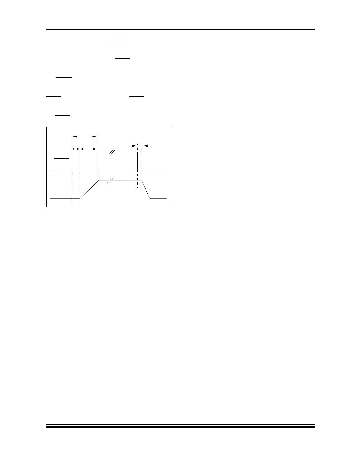
TPG
TVDET_PWRG
VPWRGD_TH
VOUT
PWRGD
VOL
VOH
V
IN
SHDN
V
OUT
30 µs
70 µs
T
OR
PWRGD
T
PG
4.4 Input Capacitor
Low input source impedance is necessary for the LDO
output to operate properly. When operating from
batteries, or in applications with long lead length
(> 10 inches) between the input source and the LDO,
some input capacitance is recommended. A minimum
of 1.0 µF to 4.7 µF is recommended for most
applications.
For applications that have output step load
requirements, the input capacitance of the LDO is very
important. The input capacitance provides the LDO
with a good local low-impedance source to pull the
transient currents from in order to respond quickly to
the output load step. For good step response
performance, the input capacitor should be of
equivalent (or higher) value than the output capacitor.
The capacitor should be placed as close to the input of
the LDO as is practical. Larger input capacitors will also
help reduce any high-frequency noise on the input and
output of the LDO and reduce the effects of any
inductance that exists between the input source
voltage and the input capacitance of the LDO.
4.5 Power Good Output (PWRGD)
The PWRGD output is used to indicate when the output
voltage of the LDO is within 92% (typical value, see
Section 1.0 “Electrical Characteristics” for Minimum
and Maximum specifications) of its nominal regulation
value.
As the output voltage of the LDO rises, the PWRGD
output will be held low until the output voltage has
exceeded the power good threshold plus the hysteresis
value. Once this threshold has been exceeded, the
power good time delay is started (shown as T
Electrical Characteristics table). The power good time
delay is fixed at 110 µs (typical). After the time delay
period, the PWRGD output will go high, indicating that
the output voltage is stable and within regulation limits.
If the output voltage of the LDO falls below the power
good threshold, the power good output will transition
low. The power good circuitry has a 170 µs delay when
detecting a falling output voltage, which helps to
increase noise immunity of the power good output and
avoid false triggering of the power good output during
fast output transients. See Figure 4-2 for power good
timing characteristics.
When the LDO is put into Shutdown mode using the
input, the power good output is pulled low
SHDN
immediately, indicating that the output voltage will be
out of regulation. The timing diagram for the power
good output when using the shutdown input is shown in
Figure 4-3.
PG
in the
The power good output is an open-drain output that can
be pulled up to any voltage that is equal to or less than
the LDO input voltage. This output is capable of sinking
1.2 mA (V
< 0.4V maximum).
PWRGD
FIGURE 4-2: Power Good Timing.
FIGURE 4-3: Power Good Timing from
Shutdown.
4.6 Shutdown Input (SHDN)
The SHDN input is an active-low input signal that turns
the LDO on and off. The SHDN
percentage of the input voltage. The typical value of
this shutdown threshold is 30% of VIN, with minimum
and maximum limits over the entire operating
temperature range of 45% and 15%, respectively.
The SHDN
input will ignore low-going pulses (pulses
meant to shut down the LDO) that are up to 400 ns in
pulse width. If the shutdown input is pulled low for more
than 400 ns, the LDO will enter Shutdown mode. This
small bit of filtering helps to reject any system noise
spikes on the shutdown input signal.
threshold is a
DS22056A-page 18 © 2007 Microchip Technology Inc.
MCP1825/MCP1825S
SHDN
V
OUT
30 µs
70 µs
T
OR
400 ns (typ)
On the rising edge of the SHDN input, the shutdown
circuitry has a 30 µs delay before allowing the LDO
output to turn on. This delay helps to reject any false
turn-on signals or noise on the SHDN
the 30 µs delay, the LDO output enters its soft-start
period as it rises from 0V to its final regulation value. If
the SHDN
delay period, the timer will be reset and the delay time
will start over again on the next rising edge of the
SHDN
high (turn-on) to the LDO output being in regulation is
typically 100 µs. See Figure 4-4 for a timing diagram of
the SHDN
input signal is pulled low during the 30 µs
input. The total time from the SHDN input going
input.
input signal. After
FIGURE 4-4: Shutdown Input Timing Diagram.
4.7 Dropout Voltage and
Undervoltage Lockout
Dropout voltage is defined as the input-to-output
voltage differential at which the output voltage drops
2% below the nominal value that was measured with a
+ 0.5V differential applied. The MCP1825/
V
R
MCP1825S LDO has a very low dropout voltage
specification of 210 mV (typical) at 500 mA of output
current. See Section 1.0 “Electrical Characteristics”
for maximum dropout voltage specifications.
The MCP1825/MCP1825S LDO operates across an
input voltage range of 2.1V to 6.0V and incorporates
input Undervoltage Lockout (UVLO) circuitry that
keeps the LDO output voltage off until the input voltage
reaches a minimum of 2.00V (typical) on the rising
edge of the input voltage. As the input voltage falls, the
LDO output will remain on until the input voltage level
reaches 1.82V (typical).
Since the MCP1825/MCP1825S LDO undervoltage
lockout activates at 1.82V as the input voltage is falling,
the dropout voltage specification does not apply for
output voltages that are less than 1.8V.
For high-current applications, voltage drops across the
PCB traces must be taken into account. The trace
resistances can cause significant voltage drops
between the input voltage source and the LDO. For
applications with input voltages near 2.1V, these PCB
trace voltage drops can sometimes lower the input
voltage enough to trigger a shutdown due to
undervoltage lockout.
4.8 Overtemperature Protection
The MCP1825/MCP1825S LDO has temperaturesensing circuitry to prevent the junction temperature
from exceeding approximately 150
junction temperature does reach 150
output will be turned off until the junction temperature
cools to approximately 140
output will automatically resume normal operation. If
the internal power dissipation continues to be
excessive, the device will again shut off. The junction
temperature of the die is a function of power
dissipation, ambient temperature and package thermal
resistance. See Section 5.0 “Application Circuits/
Issues” for more information on LDO power
dissipation and junction temperature.
°C, at which point the LDO
°C. If the LDO
°C, the LDO
© 2007 Microchip Technology Inc. DS22056A-page 19

MCP1825/MCP1825S
10 µF
V
OUT
= 2.5V @ 500 mA
R
1
C
2
10 kΩ
PWRGD
SHDN
GND
2
4.7 µF
On
Off
C
1
MCP1825-2.5
1
3
4
5
3.3V
V
IN
P
LDO
V
IN MAX)()VOUT MIN()
–()I
OUT MAX)()
×=
Where:
P
LDO
= LDO Pass device internal
power dissipation
V
IN(MAX)
= Maximum input voltage
V
OUT(MIN)
= LDO minimum output voltage
P
IGND()VIN MAX()IVIN
×=
Where:
P
I(GND
= Power dissipation due to the
quiescent current of the LDO
V
IN(MAX)
= Maximum input voltage
I
VIN
= Current flowing in the VIN pin
with no LDO output current
(LDO quiescent current)
T
JMAX()PTOTALRθJA
× T
AMAX
+=
T
J(MAX)
= Maximum continuous junction
temperature
P
TOTAL
= Total device power dissipation
Rθ
JA
= Thermal resistance from junction to
ambient
T
AMAX
= Maximum ambient temperature
5.0 APPLICATION CIRCUITS/ ISSUES
5.1 Typical Application
The MCP1825/MCP1825S is used for applications that
require high LDO output current and a power good
output.
FIGURE 5-1: Typical Application Circuit.
5.1.1 APPLICATION CONDITIONS
Package Type = TO-220-5
Input Voltage Range = 3.3V ± 5%
V
maximum = 3.465V
IN
V
minimum = 3.135V
IN
V
DROPOUT (max)
V
(typical) = 2.5V
OUT
I
P
(typical) = 0.483W
DISS
Temperature Rise = 14.2°C
5.2 Power Calculations
5.2.1 POWER DISSIPATION
The internal power dissipation within the MCP1825/
MCP1825S is a function of input voltage, output
voltage, output current and quiescent current.
Equation 5-1 can be used to calculate the internal
power dissipation for the LDO.
= 0.350V
= 500 mA maximum
OUT
In addition to the LDO pass element power dissipation,
there is power dissipation within the MCP1825/
MCP1825S as a result of quiescent or ground current.
The power dissipation as a result of the ground current
can be calculated using the following equation:
EQUATION 5-2:
The total power dissipated within the MCP1825/
MCP1825S is the sum of the power dissipated in the
LDO pass device and the P(I
CMOS construction, the typical I
MCP1825S is 120 µA. Operating at a maximum V
) term. Because of the
GND
for the MCP1825/
GND
of
IN
3.465V results in a power dissipation of 0.12 milli-Watts
for a 2.5V output. For most applications, this is small
compared to the LDO pass device power dissipation
and can be neglected.
The maximum continuous operating junction
temperature specified for the MCP1825/MCP1825S is
+125°C
. To estimate the internal junction temperature
of the MCP1825/MCP1825S, the total internal power
dissipation is multiplied by the thermal resistance from
junction to ambient (Rθ
) of the device. The thermal
JA
resistance from junction to ambient for the TO-220-5
package is estimated at 29.3° C/W.
EQUATION 5-3:
EQUATION 5-1:
DS22056A-page 20 © 2007 Microchip Technology Inc.

MCP1825/MCP1825S
P
DMAX()
T
JMAX()TAMAX()
–()
Rθ
JA
---------------------------------------------------=
P
D(MAX)
= Maximum device power dissipation
T
J(MAX)
= maximum continuous junction
temperature
T
A(MAX)
= maximum ambient temperature
Rθ
JA
= Thermal resistance from junction-to-
ambient
T
JRISE()PDMAX()RθJA
×=
T
J(RISE)
= Rise in device junction temperature
over the ambient temperature
P
D(MAX)
= Maximum device power dissipation
Rθ
JA
= Thermal resistance from junction-to-
ambient
TJT
JRISE()TA
+=
T
J
= Junction temperature
T
J(RISE)
= Rise in device junction temperature
over the ambient temperature
T
A
= Ambient temperature
The maximum power dissipation capability for a
package can be calculated given the junction-toambient thermal resistance and the maximum ambient
temperature for the application. Equation 5-4 can be
used to determine the package maximum internal
power dissipation.
EQUATION 5-4:
EQUATION 5-5:
5.3 Typical Application
Internal power dissipation, junction temperature rise,
junction temperature and maximum power dissipation
is calculated in the following example. The power dissipation as a result of ground current is small enough to
be neglected.
5.3.1 POWER DISSIPATION EXAMPLE
Package
Package Type = TO-220-5
Input Voltage
V
=3.3V ± 5%
IN
LDO Output Voltage and Current
V
=2.5V
OUT
I
=500mA
OUT
Maximum Ambient Temperature
T
Internal Power Dissipation
P
LDO(MAX)
=60°C
A(MAX)
=(V
P
= ((3.3V x 1.05) – (2.5V x 0.975))
LDO
IN(MAX)
– V
OUT(MIN)
x 500 mA
P
= 0.514 Watts
LDO
) x I
OUT(MAX)
EQUATION 5-6:
5.3.1.1 Device Junction Temperature Rise
The internal junction temperature rise is a function of
internal power dissipation and the thermal resistance
from junction-to-ambient for the application. The
thermal resistance from junction-to-ambient (Rθ
derived from EIA/JEDEC standards for measuring
thermal resistance. The EIA/JEDEC specification is
JESD51. The standard describes the test method and
board specifications for measuring the thermal
resistance from junction to ambient. The actual thermal
resistance for a particular application can vary
depending on many factors such as copper area and
thickness. Refer to AN792, “A Method to Determine
How Much Power a SOT23 Can Dissipate in an Application” (DS00792), for more information regarding this
subject.
T
J(RISE)
T
JRISE
T
JRISE
=P
= 0.514 W x 29.3° C/W
= 15.06°C
TOTAL
x Rθ
JA
JA
) is
© 2007 Microchip Technology Inc. DS22056A-page 21

MCP1825/MCP1825S
5.3.1.2 Junction Temperature Estimate
To estimate the internal junction temperature, the
calculated temperature rise is added to the ambient or
offset temperature. For this example, the worst-case
junction temperature is estimated below:
TJ =T
TJ = 15.06°C + 60.0°C
T
= 75.06°C
J
JRISE
+ T
A(MAX)
5.3.1.3 Maximum Package Power
Dissipation at 60°C Ambient
Temperature
TO-220-5 (29.3°C/W Rθ
P
P
DDPAK-5 (31.2°C/Watt RθJA):
P
P
From this table, you can see the difference in maximum
allowable power dissipation between the TO-220-5
package and the DDPAK-5 package.
= (125°C – 60°C) / 29.3°C/W
D(MAX)
= 2.218W
D(MAX)
= (125°C – 60°C)/ 31.2°C/W
D(MAX)
= 2.083W
D(MAX)
JA
):
DS22056A-page 22 © 2007 Microchip Technology Inc.
6.0 PACKAGING INFORMATION
Legend: XX...X Customer-specific information
Y Year code (last digit of calendar year)
YY Year code (last 2 digits of calendar year)
WW Week code (week of January 1 is week ‘01’)
NNN Alphanumeric traceability code
Pb-free JEDEC designator for Matte Tin (Sn)
* This package is Pb-free. The Pb-free JEDEC designator ( )
can be found on the outer packaging for this package.
Note: In the event the full Microchip part number cannot be marked on one line, it will
be carried over to the next line, thus limiting the number of available
characters for customer-specific information.
3
e
Example:3-Lead DDPAK (MCP1825S)
3-Lead TO-220 (MCP1825S)
1
23
123
XXXXXXXXX
XXXXXXXXX
YYWWNNN
XXXXXXXXX
XXXXXXXXX
YYWWNNN
123
MCP1825S
0.8EEB^^
0710256
123
MCP1825S
12EAB^^
0710256
Example:
3-Lead SOT-223 (MCP1825S)
XXXXXXX
XXXYYWW
NNN
Example:
182508
EDB0710
256
6.1 Package Marking Information
MCP1825/MCP1825S
3
e
3
e
3
e
© 2007 Microchip Technology Inc. DS22056A-page 23

MCP1825/MCP1825S
Legend: XX...X Customer-specific information
Y Year code (last digit of calendar year)
YY Year code (last 2 digits of calendar year)
WW Week code (week of January 1 is week ‘01’)
NNN Alphanumeric traceability code
Pb-free JEDEC designator for Matte Tin (Sn)
* This package is Pb-free. The Pb-free JEDEC designator ( )
can be found on the outer packaging for this package.
Note: In the event the full Microchip part number cannot be marked on one line, it will
be carried over to the next line, thus limiting the number of available
characters for customer-specific information.
5-Lead DDPAK (MCP1825)
5-Lead TO-220 (MCP1825)
12345
12345
XXXXXXXXX
XXXXXXXXX
YYWWNNN
XXXXXXXXX
XXXXXXXXX
YYWWNNN
12345
MCP1825
1.0EET^^
0710256
12345
MCP1825
08EAT^^
0710256
Example:
Example:
5-Lead SOT-223 (MCP1825)
XXXXXXX
XXXYYWW
NNN
Example:
1825-08
EDC0710
256
Package Marking Information (Continued)
3
e
3
e
3
e
3
e
DS22056A-page 24 © 2007 Microchip Technology Inc.

MCP1825/MCP1825S
3-Lead Plastic (EB) [DDPAK]
Notes:
1. § Significant Characteristic.
2. Dimensions D and E do not include mold flash or protrusions. Mold flash or protrusions shall not exceed .005" per side.
3. Dimensioning and tolerancing per ASME Y14.5M.
BSC: Basic Dimension. Theoretically exact value shown without tolerances.
Note: For the most current package drawings, please see the Microchip Packaging Specification located at
http://www.microchip.com/packaging
Units INCHES
Dimension Limits MIN NOM MAX
Number of Pins N 3
Pitch e .100 BSC
Overall Height A .160 – .190
Standoff § A1 .000 – .010
Overall Width E .380 – .420
Exposed Pad Width E1 .245 – –
Molded Package Length D .330 – .380
Overall Length H .549 – .625
Exposed Pad Length D1 .270 – –
Lead Thickness c .014 – .029
Pad Thickness C2 .045 – .065
Lower Lead Width b .020 – .039
Upper Lead Width b1 .045 – .070
Foot Length L .068 – .110
Pad Length L1 – – .067
Foot Angle φ 0° – 8°
E
E1
H
L1
D
D1
N
1
e
b
b1
c
C2
L
A
A1
BOTTOM VIEW
TOP VIEW
CHAMFER
OPTIONAL
φ
Microchip TechnologyDrawing C04-011B
© 2007 Microchip Technology Inc. DS22056A-page 25

MCP1825/MCP1825S
3-Lead Plastic Small Outline Transistor (DB) [SOT-223]
Notes:
1. Dimensions D and E1 do not include mold flash or protrusions. Mold flash or protrusions shall not exceed 0.127 mm per side.
2. Dimensioning and tolerancing per ASME Y14.5M.
BSC: Basic Dimension. Theoretically exact value shown without tolerances.
Note: For the most current package drawings, please see the Microchip Packaging Specification located at
http://www.microchip.com/packaging
Units MILLIMETERS
Dimension Limits MIN NOM MAX
Number of Leads N 3
Lead Pitch e 2.30 BSC
Outside Lead Pitch e1 4.60 BSC
Overall Height A – – 1.80
Standoff A1 0.02 – 0.10
Molded Package Height A2 1.50 1.60 1.70
Overall Width E 6.70 7.00 7.30
Molded Package Width E1 3.30 3.50 3.70
Overall Length D 6.30 6.50 6.70
Lead Thickness c 0.23 0.30 0.35
Lead Width b 0.60 0.76 0.84
Tab Lead Width b2 2. 90 3.00 3.10
Foot Length L 0.75 – –
Lead Angle φ 0° – 10°
D
b2
EE1
1
2
3
e
e1
A
A2
A1
b
c
L
φ
Microchip Technology Drawing C04-032B
DS22056A-page 26 © 2007 Microchip Technology Inc.

MCP1825/MCP1825S
3-Lead Plastic Transistor Outline (AB) [TO-220]
Notes:
1. Dimensions D and E do not include mold flash or protrusions. Mold flash or protrusions shall not exceed .005" per side.
2. Dimensioning and tolerancing per ASME Y14.5M.
BSC: Basic Dimension. Theoretically exact value shown without tolerances.
Note: For the most current package drawings, please see the Microchip Packaging Specification located at
http://www.microchip.com/packaging
Units INCHES
Dimension Limits MIN NOM MAX
Number of Pins N 3
Pitch e .100 BSC
Overall Pin Pitch e1 .200 BSC
Overall Height A .140 – .190
Tab Thickness A1 .020 – .055
Base to Lead A2 .080 – .115
Overall Width E .357 – .420
Mounting Hole Center Q .100 – .120
Overall Length D .560 – .650
Molded Package Length D1 .330 – .355
Tab Length H1 .230 – .270
Mounting Hole Diameter φP .139 – .156
Lead Length L .500 – .580
Lead Shoulder L1 – – .250
Lead Thickness c .012 – .024
Lead Width b .015 .027 .040
Shoulder Width b2 .045 .057 .070
E
Q
D
D1
L1
L
1
2
e
e1
b
b2
N
A2
c
H1
A1
A
P
CHAMFER
OPTIONAL
φ
Microchip Technology Drawing C04-034B
© 2007 Microchip Technology Inc. DS22056A-page 27

MCP1825/MCP1825S
5-Lead Plastic (ET) [DDPAK]
Notes:
1. § Significant Characteristic.
2. Dimensions D and E do not include mold flash or protrusions. Mold flash or protrusions shall not exceed .005" per side.
3. Dimensioning and tolerancing per ASME Y14.5M.
BSC: Basic Dimension. Theoretically exact value shown without tolerances.
Note: For the most current package drawings, please see the Microchip Packaging Specification located at
http://www.microchip.com/packaging
Units INCHES
Dimension Limits MIN NOM MAX
Number of Pins N 5
Pitch e .067 BSC
Overall Height A .160 – .190
Standoff § A1 .000 – .010
Overall Width E .380 – .420
Exposed Pad Width E1 .245 – –
Molded Package Length D .330 – .380
Overall Length H .549 – .625
Exposed Pad Length D1 .270 – –
Lead Thickness c .014 – .029
Pad Thickness C2 .045 – .065
Lead Width b .020 – . 039
Foot Length L .068 – .110
Pad Length L1 – – .067
Foot Angle φ 0° – 8°
E
L1
D
D1
H
N
1
b
e
TOP VIEW
BOTTOM VIEW
A
A1
c
L
C2
CHAMFER
OPTIONAL
E1
φ
Microchip Technology Drawing C04-012B
DS22056A-page 28 © 2007 Microchip Technology Inc.

MCP1825/MCP1825S
/HDG3ODVWLF6PDOO2XWOLQH7UDQVLVWRU'&>627@
1RWHV
'LPHQVLRQV'DQG(GRQRWLQFOXGHPROGIODVKRUSURWUXVLRQV0ROGIODVKRUSURWUXVLRQVVKDOOQRWH[FHHGPPSHUVLGH
'LPHQVLRQLQJDQGWROHUDQFLQJSHU$60(<0
%6& %DVLF'LPHQVLRQ7KHRUHWLFDOO\H[DFWYDOXHVKRZQZLWKRXWWROHUDQFHV
1RWH )RUWKHPRVWFXUUHQWSDFNDJHGUDZLQJVSOHDVHVHHWKH0LFURFKLS3DFNDJLQJ6SHFLILFDWLRQORFDWHGDW
KWWSZZZPLFURFKLSFRPSDFNDJLQJ
8QLWV 0,//,0(7(56
'LPHQVLRQ/LPLWV 0,1 120 0$;
1XPEHURI/HDGV 1
/HDG3LWFK H %6&
2XWVLGH/HDG3LWFK H %6&
2YHUDOO+HLJKW $ ± ±
6WDQGRII $
0ROGHG3DFNDJH+HLJKW $
2YHUDOO:LGWK (
0ROGHG3DFNDJH:LGWK (
2YHUDOO/HQJWK '
/HDG7KLFNQHVV F
/HDG:LGWK E
7DE/HDG:LGWK E
)RRW/HQJWK / ±
/HDG$QJOH
D
b2
E
E1
1
2
34
N
e
e1
A2
A
b
A1
c
L
φ
0LFURFKLS 7HFKQRORJ\ 'UDZLQJ &%
© 2007 Microchip Technology Inc. DS22056A-page 29

MCP1825/MCP1825S
5-Lead Plastic Transistor Outline (AT) [TO-220]
Notes:
1. Dimensions D and E do not include mold flash or protrusions. Mold flash or protrusions shall not exceed .005" per side.
2. Dimensioning and tolerancing per ASME Y14.5M.
BSC: Basic Dimension. Theoretically exact value shown without tolerances.
Note: For the most current package drawings, please see the Microchip Packaging Specification located at
http://www.microchip.com/packaging
Units INC HES
Dimension Limits MIN NOM MAX
Number of Pins N 5
Pitch e .067 BSC
Overall Pin Pitch e1 .268 BSC
Overall Height A .140 – .190
Overall Width E .380 – .420
Overall Length D .560 – .650
Molded Package Length D1 .330 – .355
Tab Length H1 .204 – .293
Tab Thickness A1 .020 – .055
Mounting Hole Center Q .100 – .120
Mounting Hole Diameter φP .139 – .156
Lead Length L .482 – .590
Base to Bottom of Lead A2 .080 – .115
Lead Thickness c .012 – .025
Lead Width b .015 .027 .040
E
Q
D
D1
H1
A
A1
A2
c
N
e
e1
b
1
2
3
L
CHAMFER
OPTIONAL
Pφ
Microchip Technology Drawing C04-036B
DS22056A-page 30 © 2007 Microchip Technology Inc.

APPENDIX A: REVISION HISTORY
Revision A (August 2007)
• Original Release of this Document.
MCP1825/MCP1825S
© 2007 Microchip Technology Inc. DS22056A-page 31

MCP1825/MCP1825S
NOTES:
DS22056A-page 32 © 2007 Microchip Technology Inc.

MCP1825/MCP1825S
Device: MCP1825: 500 mA Low Dropout Regulator
MCP1825T: 500 mA Low Dropout Regulator
Tape and Reel
MCP1825S: 500 mA Low Dropout Regulator
MCP1825ST: 500 mA Low Dropout Regulator
Tape and Reel
Output Voltage *: 08 = 0.8V “Standard”
12 = 1.2V “Standard”
18 = 1.8V “Standard”
25 = 2.5V “Standard”
30 = 3.0V “Standard”
33 = 3.3V “Standard”
50 = 5.0V “Standard”
ADJ = Adjustable Output Voltage ** (MCP1825 Only)
*Contact factory for other output voltage options
** When ADJ is used, the “extra feature code” and
“tolerance” columns do not apply. Refer to examples.
Extra Feature Code: 0 = Fixed
Tolerance: 2 = 2.0% (Standard)
Temperature: E = -40°C to +125°C
Package Type: AB = Plastic Transistor Outline, TO-220, 3-lead
AT = Plastic Transistor Outline, TO-220, 5-lead
EB = Plastic, DDPAK, 3-lead
ET = Plastic, DDPAK, 5-lead
DB = Plastic Small Transistor Outline, SOT-223, 3-lead
DC = Plastic Small Transistor Outline, SOT-223, 5-lead
Note: ADJ (Adjustable) only available in 5-lead version.
PART NO. XXX
Output Feature
Code
Device
Vol tag e
X
Tol era nceX/Tem p.XXPackage
Examples:
a) MCP1825-0802E/XX: 0.8V LDO Regulator
b) MCP1825-1002E/XX: 1.0V LDO Regulator
c) MCP1825-1202E/XX: 1.2V LDO Regulator
d) MCP1825-1802E/XX: 1.8V LDO Regulator
e) MCP1825-2502E/XX: 2.5V LDO Regulator
f) MCP1825-3002E/XX: 3.0V LDO Regulator
g) MCP1825-3302E/XX: 3.3V LDO Regulator
h) MCP1825-5002E/XX: 5.0V LDO Regulator
i) MCP1825-ADJE/XX: ADJ LDO Regulator
a) MCP1825S-0802E/XX:0.8V LDO Regulator
b) MCP1825S-0802E/XX:0.8V LDO Regulator
c) MCP1825S-1002E/XX:1.0V LDO Regulator
d) MCP1825S-1202E/XX:1.2V LDO Regulator
e) MCP1825S-1802E/XX:1.8V LDO Regulator
f) MCP1825S-2502E/XX:2.5V LDO Regulator
g) MCP1825S-2502E/XX:3.0V LDO Regulator
h) MCP1825S-3302E/XX:3.3V LDO Regulator
i) MCP1825S-5002E/XX:5.0V LDO Regulator
XX = AB for 3LD TO-220 package
= AT for 5LD TO-220 package
= DB for 3LD SOT-223 package
= DC for 5LD SOT-223 package
= EB for 3LD DDPAK package
= ET for 5LD DDPAK package
PRODUCT IDENTIFICATION SYSTEM
To order or obtain information, e.g., on pricing or delivery, refer to the factory or the listed sales office.
© 2007 Microchip Technology Inc. DS22056A-page 33

MCP1825/MCP1825S
NOTES:
DS22056A-page 34 © 2007 Microchip Technology Inc.

Note the following details of the code protection feature on Microchip devices:
• Microchip products meet the specification contained in their particular Microchip Data Sheet.
• Microchip believes that its family of products is one of the most secure families of its kind on the market today, when used in the
intended manner and under normal conditions.
• There are dishonest and possibly illegal methods used to breach the code protection feature. All of these methods, to our
knowledge, require using the Microchip products in a manner outside the operating specifications contained in Microchip’s Data
Sheets. Most likely, the person doing so is engaged in theft of intellectual property.
• Microchip is willing to work with the customer who is concerned about the integrity of their code.
• Neither Microchip nor any other semiconductor manufacturer can guarantee the security of their code. Code protection does not
mean that we are guaranteeing the product as “unbreakable.”
Code protection is constantly evolving. We at Microchip are committed to continuously improving the code protection features of our
products. Attempts to break Microchip’s code protection feature may be a violation of the Digital Millennium Copyright Act. If such acts
allow unauthorized access to your software or other copyrighted work, you may have a right to sue for relief under that Act.
Information contained in this publication regarding device
applications and the like is provided only for your convenience
and may be superseded by updates. It is your responsibility to
ensure that your application meets with your specifications.
MICROCHIP MAKES NO REPRESENTATIONS OR
WARRANTIES OF ANY KIND WHETHER EXPRESS OR
IMPLIED, WRITTEN OR ORAL, STATUTORY OR
OTHERWISE, RELATED TO THE INFORMATION,
INCLUDING BUT NOT LIMITED TO ITS CONDITION,
QUALITY, PERFORMANCE, MERCHANTABILITY OR
FITNESS FOR PURPOSE. Microchip disclaims all liability
arising from this information and its use. Use of Microchip
devices in life support and/or safety applications is entirely at
the buyer’s risk, and the buyer agrees to defend, indemnify and
hold harmless Microchip from any and all damages, claims,
suits, or expenses resulting from such use. No licenses are
conveyed, implicitly or otherwise, under any Microchip
intellectual property rights.
Trademarks
The Microchip name and logo, the Microchip logo, Accuron,
dsPIC, K
EELOQ, KEELOQ logo, microID, MPLAB, PIC,
PICmicro, PICSTART, PRO MATE, rfPIC and SmartShunt are
registered trademarks of Microchip Technology Incorporated
in the U.S.A. and other countries.
AmpLab, FilterLab, Linear Active Thermistor, Migratable
Memory, MXDEV, MXLAB, SEEVAL, SmartSensor and The
Embedded Control Solutions Company are registered
trademarks of Microchip Technology Incorporated in the
U.S.A.
Analog-for-the-Digital Age, Application Maestro, CodeGuard,
dsPICDEM, dsPICDEM.net, dsPICworks, dsSPEAK, ECAN,
ECONOMONITOR, FanSense, FlexROM, fuzzyLAB,
In-Circuit Serial Programming, ICSP, ICEPIC, Mindi, MiWi,
MPASM, MPLAB Certified logo, MPLIB, MPLINK, PICkit,
PICDEM, PICDEM.net, PICLAB, PICtail, PowerCal,
PowerInfo, PowerMate, PowerTool, REAL ICE, rfLAB, Select
Mode, Smart Serial, SmartTel, Total Endurance, UNI/O,
WiperLock and ZENA are trademarks of Microchip
Technology Incorporated in the U.S.A. and other countries.
SQTP is a service mark of Microchip Technology Incorporated
in the U.S.A.
All other trademarks mentioned herein are property of their
respective companies.
© 2007, Microchip Technology Incorporated, Printed in the
U.S.A., All Rights Reserved.
Printed on recycled paper.
Microchip received ISO/TS-16949:2002 certification for its worldwide
headquarters, design and wafer fabrication facilities in Chandler and
Tempe, Arizona; Gresham, Oregon and design centers in California
and India. The Company’s quality system processes and procedures
are for its PIC
devices, Serial EEPROMs, microperipherals, nonvolatile memory and
analog products. In addition, Microchip’s quality system for the design
and manufacture of development systems is ISO 9001:2000 certified.
®
MCUs and dsPIC® DSCs, KEELOQ
®
code hopping
© 2007 Microchip Technology Inc. DS22056A-page 35

WORLDWIDE SALES AND SERVICE
AMERICAS
Corporate Office
2355 West Chandler Blvd.
Chandler, AZ 85224-6199
Tel: 480-792-7200
Fax: 480-792-7277
Technical Support:
http://support.microchip.com
Web Address:
www.microchip.com
Atlanta
Duluth, GA
Tel: 678-957-9614
Fax: 678-957-1455
Boston
Westborough, MA
Tel: 774-760-0087
Fax: 774-760-0088
Chicago
Itasca, IL
Tel: 630-285-0071
Fax: 630-285-0075
Dallas
Addison, TX
Tel: 972-818-7423
Fax: 972-818-2924
Detroit
Farmington Hills, MI
Tel: 248-538-2250
Fax: 248-538-2260
Kokomo
Kokomo, IN
Tel: 765-864-8360
Fax: 765-864-8387
Los Angeles
Mission Viejo, CA
Tel: 949-462-9523
Fax: 949-462-9608
Santa Clara
Santa Clara, CA
Tel: 408-961-6444
Fax: 408-961-6445
Toronto
Mississauga, Ontario,
Canada
Tel: 905-673-0699
Fax: 905-673-6509
ASIA/PACIFIC
Asia Pacific Office
Suites 3707-14, 37th Floor
Tower 6, The Gateway
Harbour City, Kowloon
Hong Kong
Tel: 852-2401-1200
Fax: 852-2401-3431
Australia - Sydney
Tel: 61-2-9868-6733
Fax: 61-2-9868-6755
China - Beijing
Tel: 86-10-8528-2100
Fax: 86-10-8528-2104
China - Chengdu
Tel: 86-28-8665-5511
Fax: 86-28-8665-7889
China - Fuzhou
Tel: 86-591-8750-3506
Fax: 86-591-8750-3521
China - Hong Kong SAR
Tel: 852-2401-1200
Fax: 852-2401-3431
China - Qingdao
Tel: 86-532-8502-7355
Fax: 86-532-8502-7205
China - Shanghai
Tel: 86-21-5407-5533
Fax: 86-21-5407-5066
China - Shenyang
Tel: 86-24-2334-2829
Fax: 86-24-2334-2393
China - Shenzhen
Tel: 86-755-8203-2660
Fax: 86-755-8203-1760
China - Shunde
Tel: 86-757-2839-5507
Fax: 86-757-2839-5571
China - Wuhan
Tel: 86-27-5980-5300
Fax: 86-27-5980-5118
China - Xian
Tel: 86-29-8833-7252
Fax: 86-29-8833-7256
ASIA/PACIFIC
India - Bangalore
Tel: 91-80-4182-8400
Fax: 91-80-4182-8422
India - New Delhi
Tel: 91-11-4160-8631
Fax: 91-11-4160-8632
India - Pune
Tel: 91-20-2566-1512
Fax: 91-20-2566-1513
Japan - Yokohama
Tel: 81-45-471- 6166
Fax: 81-45-471-6122
Korea - Daegu
Tel: 82-53-744-4301
Fax: 82-53-744-4302
Korea - Seoul
Tel: 82-2-554-7200
Fax: 82-2-558-5932 or
82-2-558-5934
Malaysia - Penang
Tel: 60-4-646-8870
Fax: 60-4-646-5086
Philippines - Manila
Tel: 63-2-634-9065
Fax: 63-2-634-9069
Singapore
Tel: 65-6334-8870
Fax: 65-6334-8850
Taiwan - Hsin Chu
Tel: 886-3-572-9526
Fax: 886-3-572-6459
Taiwan - Kaohsiung
Tel: 886-7-536-4818
Fax: 886-7-536-4803
Taiwan - Taipei
Tel: 886-2-2500-6610
Fax: 886-2-2508-0102
Thailand - Bangkok
Tel: 66-2-694-1351
Fax: 66-2-694-1350
EUROPE
Austria - Wels
Tel: 43-7242-2244-39
Fax: 43-7242-2244-393
Denmark - Copenhagen
Tel: 45-4450-2828
Fax: 45-4485-2829
France - Paris
Tel: 33-1-69-53-63-20
Fax: 33-1-69-30-90-79
Germany - Munich
Tel: 49-89-627-144-0
Fax: 49-89-627-144-44
Italy - Milan
Tel: 39-0331-742611
Fax: 39-0331-466781
Netherlands - Drunen
Tel: 31-416-690399
Fax: 31-416-690340
Spain - Madrid
Tel: 34-91-708-08-90
Fax: 34-91-708-08-91
UK - Wokingham
Tel: 44-118-921-5869
Fax: 44-118-921-5820
06/25/07
DS22056A-page 36 © 2007 Microchip Technology Inc.
 Loading...