

MCP1602
V
IN
V
IN
8
7
6
54
3
2
1 SHDN
V
CC
PG
A
GNDVOUT/VFB
L
X
P
GND
8
7
6
54
3
2
1
SHDN
V
CC
PG
A
GND
V
OUT/VFB
L
X
P
GND
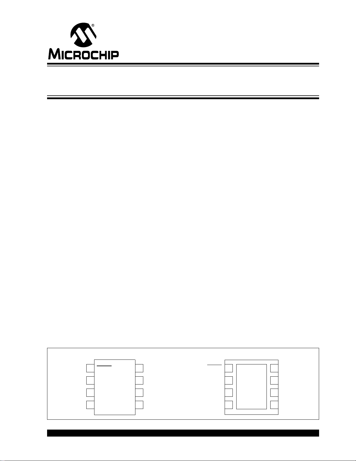
3x3 DFN-8MSOP-8
2.0 MHz, 500 mA Synchronous Buck Regulator
with Power-Good
Features
• Over 90% Typical Efficiency
• Output Current: Up To 500 mA
• Power-Good Output with 262 ms Delay
• Low Quiescent Current: 45 µA (typical)
• Low Shutdown Current: 0.05 µA (typical)
• Automatic PWM to PFM Mode Transition
• Adjustable Output Voltage:
- 0.8V to 4.5V
• Fixed Output Voltage:
- 1.2V, 1.5V, 1.8V, 2.5V, and 3.3V
• 2.0 MHz Fixed-Frequency PWM (Heavy Load)
• Internally Compensated
• Undervoltage Lockout (UVLO)
• Overtemperture Protection
• Overcurrent Protection
• Space Saving Packages:
- 8-Lead MSOP
- 8-Lead 3x3 DFN
Applications
• Cellular Telephones
• Portable Computers
• Organizers / PDAs
• USB Powered Devices
• Digital Cameras
• Portable Equipment
• +5V or +3.3V Distributed Systems
General Description
The MCP1602 is a high efficient, fully integrated
500 mA synchronous buck regulator with a powergood monitor. The 2.7V to 5.5V input voltage range and
low quiescent current (45 µA, typical) makes the
MCP1602 ideally suited for applications powered from
1-cell Li-Ion or 2-cell/3-cell NiMH/NiCd batteries.
At heavy loads, the MCP1602 operates in the 2.0 MHz
fixed frequency PWM mode which provides a low
noise, low output ripple, small-size solution. When the
load is reduced to light levels, the MCP1602
automatically changes operation to a PFM mode to
minimize quiescent current draw from the battery. No
intervention is necessary for a smooth transition from
one mode to another. These two modes of operation
allow the MCP1602 to achieve the highest efficiency
over the entire operating current range.
The open-drain power-good feature of the MCP1602
monitors the output voltage and provides indication
when the output voltage is within 94% (typical) of the
regulation value. The typical 2% hystereses in the
power-good transition threshold as well as a
262 ms (typical) delay time ensures accurate powergood signaling.
The MCP1602 is available in either the 8-pin DFN or
MSOP package. It is also available with either an
adjustable or fixed output voltage. The available fixed
output voltage options are 1.2V, 1.5V, 1.8V, 2.5V, and
3.3V.
Additional protection features include: UVLO,
overtemperature, and overcurrent protection.
Package Types
© 2007 Microchip Technology Inc. DS22061A-page 1
MCP1602
SHDN
V
CC
PG
A
GND
V
FB
V
IN
L
X
P
GND
1
2
3
4
8
7
6
5
ON
OFF
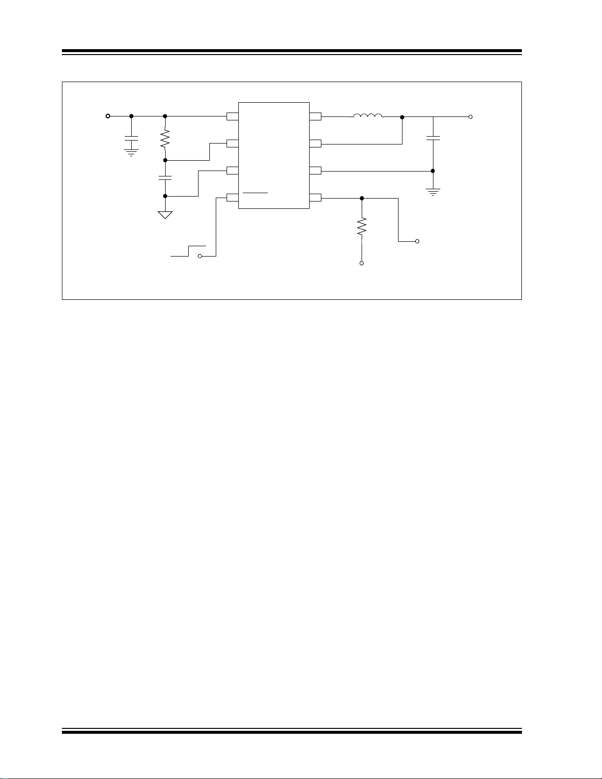
MCP1602
V
IN
2.7V to 4.5V
V
OUT
1.5V @ 500 mA
V
IN
R
PULLUP
4.7 µF
4.7 µH
4.7 µF
0.1 µF
10Ω
Processor
Reset
Typical Application Circuit
DS22061A-page 2 © 2007 Microchip Technology Inc.
ILIM
PWM
ILIM
PFM
IPEAK
PWM
IPEAK
PFM
V
IN
SHDN
VFB/V
OUT
P
GND
L
X
Band
Gap
UVLO
Switch Drive
UVLO
V
REF
Logic and Timing
S
RQ
Q
Soft Start
V
REF
PWM/PFM
Logic
V
REF
Slope
Comp
OSC
-IPK Limit
Thermal
Shutdown
TSD
EA
POFF NOFF
PWM/PFM
PFM Error Amp
PWM Error Amp
OV Threshold
UV Threshold
IPK Limit
-ILPK
IPEAK
PWM
IPEAK
PFM
Disable
Switcher
-ILPK
PG Generator
with Delay
V
REF
V
CC
V
OUT
A
GND
PG
V
CC
Functional Block Diagram
MCP1602
© 2007 Microchip Technology Inc. DS22061A-page 3
MCP1602
1.0 ELECTRICAL CHARACTERISTICS
Absolute Maximum Ratings †
VIN - A
All Other I/O ..............................(A
LX to P
Output Short Circuit Current..................................Continuous
Power Dissipation (Note 6) ..........................Internally Limited
Storage Temperature.................................... -65
Ambient Temp. with Power Applied................ -40
Operating Junction Temperature.................. -40
ESD Protection On All Pins:
HBM..............................................................................3 kV
MM............................................................................... 200V
......................................................................+6.0V
GND
............................................. -0.3V to (VIN + 0.3V)
GND
- 0.3V) to (VIN + 0.3V)
GND
o
C to +150oC
o
C to +85oC
o
C to +125oC
† Notice: Stresses above those listed under "Maximum
Ratings" may cause permanent damage to the device. This is
a stress rating only and functional operation of the device at
those or any other conditions above those indicated in the
operational sections of this specification is not intended.
Exposure to maximum rating conditions for extended periods
may affect device reliability.
DC CHARACTERISTICS
Electrical Characteristics: Unless otherwise indicated, VIN = 3.6V, C
(ADJ) = 1.8V, I
V
OUT
= 100 mA, TA = +25°C. Boldface specifications apply for the TA range of -40
OUT
Parameters Sym Min Typ Max Units Conditions
Input Characteristics
Input Voltage V
Maximum Output Current I
Shutdown Current I
IN_SHDN
Quiescent Current I
IN
OUT
Q
2.7 — 5.5 V Note 1
500 ——mANote 1
— 0.05 1 µA SHDN = GND
—4560 µA SHDN = VIN, I
Shutdown/UVLO/Thermal Shutdown Characteristics
SHDN
, Logic Input Voltage Low V
SHDN
, Logic Input Voltage High V
SHDN, Input Leakage Current V
IL
IH
L_SHND
——15 %VINVIN = 2.7V to 5.5V
45 ——%VINVIN = 2.7V to 5.5V
-1.0 ±0.1 1.0 µA VIN = 2.7V to 5.5V, SHDN =A
Undervoltage Lockout UVLO 2.40 2.55 2.70 VVIN Falling
Undervoltage Lockout Hystere-
UVLO
— 200 — mV
HYS
sis
Thermal Shutdown T
Thermal Shutdown Hysteresis T
SHD-HYS
SHD
— 150 — °C Note 5, Note 6
—10— °CNote 5, Note 6
Output Characteristics
Adjustable Output Voltage
V
OUT
0.8 — 4.5 V Note 2
Range
Reference Feedback Voltage V
Feedback Input Bias Current I
Note 1: The minimum V
has to meet two conditions: VIN ≥ 2.7V and VIN ≥ V
IN
FB
VFB
—0.8— V
— -1.5 — nA
2: Reference Feedback Voltage Tolerance applies to adjustable output voltage setting.
is the output voltage setting.
3: V
R
4: Regulation is measured at a constant junction temperature using low duty cycle pulse testing. Load
regulation is tested over a load range of 0.1 mA to the maximum specified output current. Changes in
output voltage due to heating effects are covered by the thermal regulation specification.
5: The maximum allowable power dissipation is a function of ambient temperature, the maximum allowable
temperature and the thermal resistance from junction to air (i.e. T
allowable power dissipation causes the device to initiate thermal shutdown.
6: The internal MOSFET switches have an integral diode from the L
to the GND pin. In cases where these diodes are forward-biased, the package power dissipation limits
must be adhered too. Thermal protection is not able to limit the junction temperature for these cases.
7: The current limit threshold is a cycle-by-cycle current limit.
= CIN = 4.7 µF, L = 4.7 µH,
OUT
= 0 mA
OUT
+ 0.5V.
OUT
, TJ, θJA). Exceeding the maximum
A
pin to the VIN pin, and from the LX pin
X
o
C to +85
o
GND
C.
DS22061A-page 4 © 2007 Microchip Technology Inc.
MCP1602
DC CHARACTERISTICS (CONTINUED)
Electrical Characteristics: Unless otherwise indicated, VIN = 3.6V, C
V
(ADJ) = 1.8V, I
OUT
= 100 mA, TA = +25°C. Boldface specifications apply for the TA range of -40
OUT
Parameters Sym Min Typ Max Units Conditions
Output Voltage Tolerance Fixed V
Line Regulation V
Load Regulation V
Internal Oscillator Frequency F
Start Up Time T
R
P-Channel R
DSon
R
N-Channel R
DSon
L
Pin Leakage Current I
X
Positive Current Limit Threshold +I
LX(MAX)
OUT
LINE-
REG
LOAD-
REG
OSC
SS
DSon-P
DSon-N
LX
-2.5 V
+2.5 % Note 3
R
—0.3—%/VVIN = VR + 1V to 5.5V,
—0.4— %VIN=VR+1.5V,
1.6 2.0 2.4 MHz
—0.5— msTR= 10% to 90%
— 450 — mΩ IP=100mA
— 450 — mΩ IN= 100 mA
-1.0 ±0.01 1.0 µA SHDN =0V, VIN= 5.5V, LX=0V,
— 700 — mA Note 7
Power-Good (PG)
Voltage Range V
PG Threshold High V
PG Threshold Low V
PG Threshold Hysteresis V
TH_HYS
PG
TH_H
TH_L
1.0
1.2
—5.5
5.5
—9496 % of
89 92 — % of
—2—% of
PG Threshold Tempco ΔVTH/ΔT— 30 —ppm/°C
PG Delay t
PG Active Time-out Period t
RPD
RPU
PG Output Voltage Low PG_V
Note 1: The minimum V
has to meet two conditions: VIN ≥ 2.7V and VIN ≥ V
IN
— 165 — µs V
140 262 560 ms V
——0.2 VV
OL
2: Reference Feedback Voltage Tolerance applies to adjustable output voltage setting.
is the output voltage setting.
3: V
R
4: Regulation is measured at a constant junction temperature using low duty cycle pulse testing. Load
regulation is tested over a load range of 0.1 mA to the maximum specified output current. Changes in
output voltage due to heating effects are covered by the thermal regulation specification.
5: The maximum allowable power dissipation is a function of ambient temperature, the maximum allowable
temperature and the thermal resistance from junction to air (i.e. T
allowable power dissipation causes the device to initiate thermal shutdown.
6: The internal MOSFET switches have an integral diode from the L
to the GND pin. In cases where these diodes are forward-biased, the package power dissipation limits
must be adhered too. Thermal protection is not able to limit the junction temperature for these cases.
7: The current limit threshold is a cycle-by-cycle current limit.
= CIN = 4.7 µF, L = 4.7 µH,
OUT
=100mA
I
OUT
I
= 100 mA to 500 mA, Note 1
LOAD
LX=5.5V
VTA= 0°C to +70°C
= -40°C to +85°C
T
A
VIN≤ 2.7V, I
On Rising V
V
OUT
On Falling V
V
OUT
V
OUT
=(V
OUT
(V
- 100 mV)
TH_L
=(V
OUT
(V
I
I
OUT
, TJ, θJA). Exceeding the maximum
A
pin to the VIN pin, and from the LX pin
X
+100mV), I
TH_H
OUT=VTH_L
= 1.2 mA, VIN>2.7V
PG
= 100 µA, 1.0 < VIN<2.7V
PG
+ 0.5V.
SINK
OUT
OUT
+ 100 mV) to
TH_H
-100mV) to
TH_L
-100mV,
= 100 µA
o
C to +85
SINK
o
=1.2mA
C.
© 2007 Microchip Technology Inc. DS22061A-page 5
MCP1602
TEMPERATURE SPECIFICATIONS
Electrical Specifications: Unless otherwise indicated, all limits are specified for: VIN+2.7Vto5.5V
Parameters Sym Min Typ Max Units Conditions
Temperature Ranges
Operating Junction Temperature
Range
Storage Temperature Range T
Maximum Junction Temperature T
Package Thermal Resistances
Thermal Resistance, 8L-MSOP θ
Thermal Resistance, 8L-3x3 DFN θ
T
J
A
J
JA
JA
-40 — +125 °C Steady State
-65 — +150 °C
— — +150 °C Transient
— 211 — °C/W Typical 4-layer Board with
Internal Ground Plane
— 60 — °C/W Typical 4-layer Board with
Internal Ground Plane and
2-Vias in Thermal Pad
DS22061A-page 6 © 2007 Microchip Technology Inc.
MCP1602
30
35
40
45
50
55
60
-40 -25 -10 5 20 35 50 65 80 95 110 125
Ambient Temperature (
o
C)
Quiescent Current (µA)
V
OUT
= 1.8V
VIN = 5.5V
VIN = 3.6V
VIN = 4.2V
65
70
75
80
85
90
95
100
3.0 3.2 3.4 3.6 3.8 4.0 4.2
Input Voltage (V)
Efficiency (%)
V
OUT
= 1.2V
I
OUT
= 100 mA
I
OUT
= 500 mA
I
OUT
= 300 mA
70
75
80
85
90
95
100
3.0 3.2 3.4 3.6 3.8 4.0 4.2
Input Voltage (V)
Efficiency (%)
V
OUT
= 1.8V
I
OUT
= 100 mA
I
OUT
= 500 mA
I
OUT
= 300 mA
30
35
40
45
50
55
2.7 3.05 3.4 3.75 4.1 4.45 4.8 5.15 5.5
Input Voltage (V)
Quiescent Current (µA)
TA = +90°CTA = +25°C
TA = -40°C
20
30
40
50
60
70
80
90
100
0.1 1 10 100 1000
Output Current (mA)
Efficiency (%)
V
OUT
= 1.2V
VIN = 3.0V
VIN = 3.6V
VIN = 4.2V
20
30
40
50
60
70
80
90
100
0.1 1 10 100 1000
Output Current (mA)
Efficiency (%)
V
OUT
= 1.8V
VIN = 3.0V
VIN = 3.6V
VIN = 4.2V
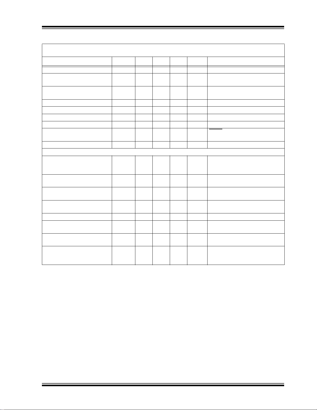
2.0 TYPICAL PERFORMANCE CURVES
Note: The graphs and tables provided following this note are a statistical summary based on a limited number of
samples and are provided for informational purposes only. The performance characteristics listed herein are
not tested or guaranteed. In some graphs or tables, the data presente d may be outside the specified
operating range (e.g., outside specified power supply range) and therefore outside the warranted range.
Note: Unless otherwise indicated, VIN= SHDN =3.6V, C
T
= +25°C. Adjustable or fixed output voltage options can be used to generate the Typical Performance Characteristics.
A
OUT=CIN
FIGURE 2-1: IQ vs. Ambient Temperature.
= 4.7 µF, L = 4.7 µH, V
FIGURE 2-4: I
(ADJ) = 1.8V, I
OUT
vs. Input Voltage.
Q
LOAD
= 100 mA,
FIGURE 2-2: Efficiency vs. Input Voltage
= 1.2V).
(V
OUT
FIGURE 2-3: Efficiency vs. Input Voltage
= 1.8V).
(V
OUT
© 2007 Microchip Technology Inc. DS22061A-page 7
FIGURE 2-5: Efficiency vs. Output Load
= 1.2V).
(V
OUT
FIGURE 2-6: Efficiency vs. Output Load
= 1.8V).
(V
OUT

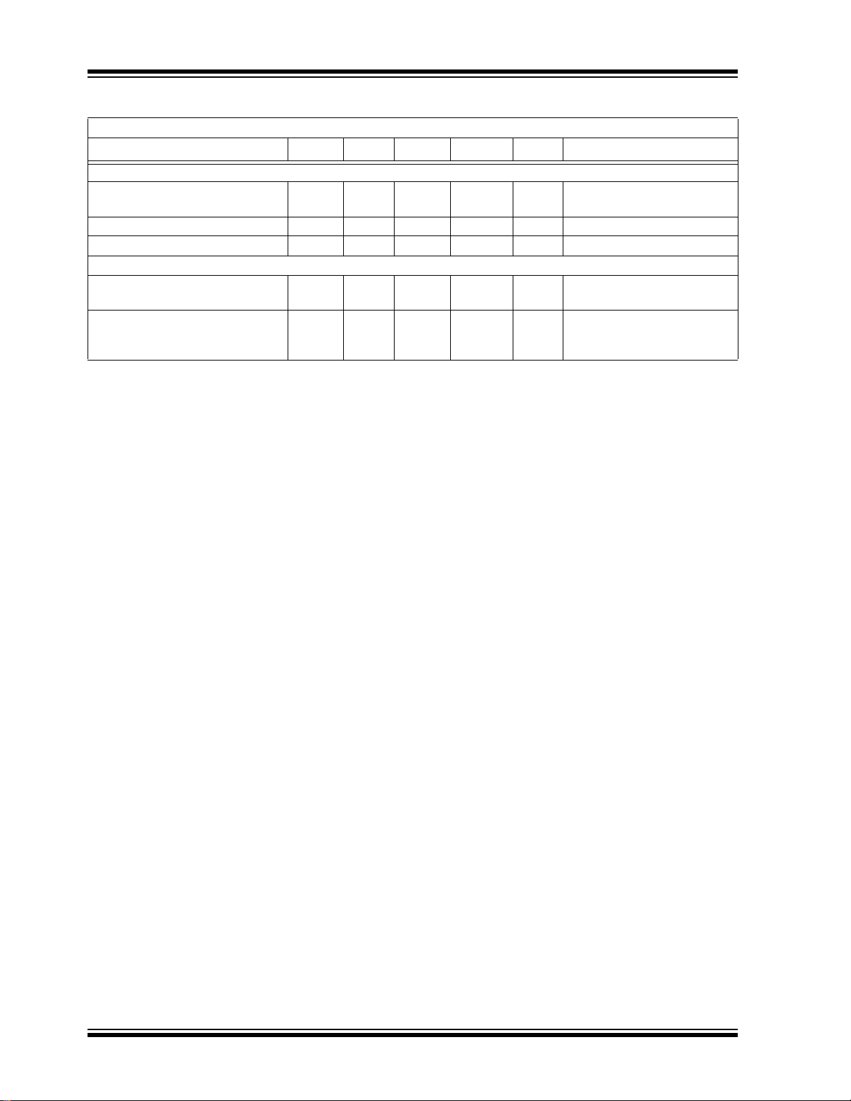
MCP1602
85.0
87.5
90.0
92.5
95.0
97.5
100.0
4.2 4.4 4.6 4.8 5.0 5.2 5.4
Input Voltage (V)
Efficiency (%)
V
OUT
= 3.3V
I
OUT
= 100 mA
I
OUT
= 500 mA
I
OUT
= 300 mA
200
220
240
260
280
300
320
340
-40 -25 -10 5 20 35 50 65 80 95 110 125
Ambient Temperature (°C)
PG Active Time-Out (ms)
0.812
0.816
0.820
0.824
0.828
0.832
-40
-25
-10
5
2035506580
95
110
125
Ambient Temperature (°C)
Feedback Voltage (V)
20
30
40
50
60
70
80
90
100
0.1 1 10 100 1000
Output Current (mA)
Efficiency (%)
V
OUT
= 3.3VVIN = 5.5V
VIN = 4.2V
88
89
90
91
92
93
94
95
96
-40 -25 -10 5 20 35 50 65 80 95 110 125
Ambient Temperature (°C)
PG Threshold (% of V
OUT
)
PG Threshold High
PG Threshold Low
1.81
1.82
1.83
1.84
1.85
0 50 100 150 200 250 300 350 400 450 500
Output Current (mA)
Output Voltage (V)
Typical Performance Curves (Continued)
Note: Unless otherwise indicated, VIN= SHDN =3.6V, C
T
= +25°C. Adjustable or fixed output voltage options can be used to generate the Typical Performance Characteristics.
A
OUT=CIN
= 4.7 µF, L = 4.7 µH, V
(ADJ) = 1.8V, I
OUT
LOAD
= 100 mA,
FIGURE 2-7: Efficiency vs. Input Voltage
(V
= 3.3V).
OUT
FIGURE 2-8: PG Active Time-out vs. Ambient Temperature.
FIGURE 2-10: Efficiency vs. Output Load
(V
= 3.3V).
OUT
FIGURE 2-11: PG Threshold Voltage vs. Ambient Temperature.
FIGURE 2-9: Feedback Voltage vs. Ambient Temperature.
DS22061A-page 8 © 2007 Microchip Technology Inc.
FIGURE 2-12: Output Voltage vs. Load
Current (V
OUT
= 1.8V).
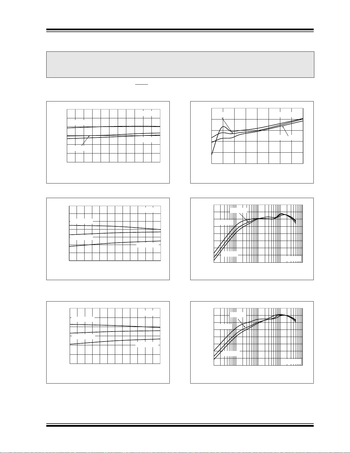
MCP1602
1.90
1.92
1.94
1.96
1.98
2.00
-40 -25 -10 5 20 35 50 65 80 95 110 125
Ambient Temperature (°C)
Switching Frequency (MHz)
0.2
0.3
0.4
0.5
0.6
2.70 3.05 3.40 3.75 4.10 4.45 4.80 5.15 5.50
Input Voltage (V)
Switch Resistance (Ω)
N-Channel
P-Channel
1.85
1.90
1.95
2.00
2.05
2.10
2.70 3.05 3.40 3.75 4.10 4.45 4.80 5.15 5.50
Input Voltage (V)
Switching Frequency (MHz)
0.2
0.3
0.4
0.5
0.6
0.7
-40 -25 -10 5 20 35 50 65 80 95 110 125
Ambient Temperature (°C)
Switch Resistance (Ω)
N-Channel
P-Channel
Typical Performance Curves (Continued)
Note: Unless otherwise indicated, VIN= SHDN =3.6V, C
T
= +25°C. Adjustable or fixed output voltage options can be used to generate the Typical Performance Characteristics.
A
OUT=CIN
= 4.7 µF, L = 4.7 µH, V
(ADJ) = 1.8V, I
OUT
LOAD
= 100 mA,
FIGURE 2-13: Switching Frequency vs. Ambient Temperature.
FIGURE 2-14: Switch Resistance vs. Input Voltage.
FIGURE 2-16: Switching Frequency vs. Input Voltage.
FIGURE 2-17: Switch Resistance vs. Ambient Temperature.
FIGURE 2-15: Output Voltage S tartup Waveform.
© 2007 Microchip Technology Inc. DS22061A-page 9
FIGURE 2-18: Heavy Load Switching Waveform.

MCP1602
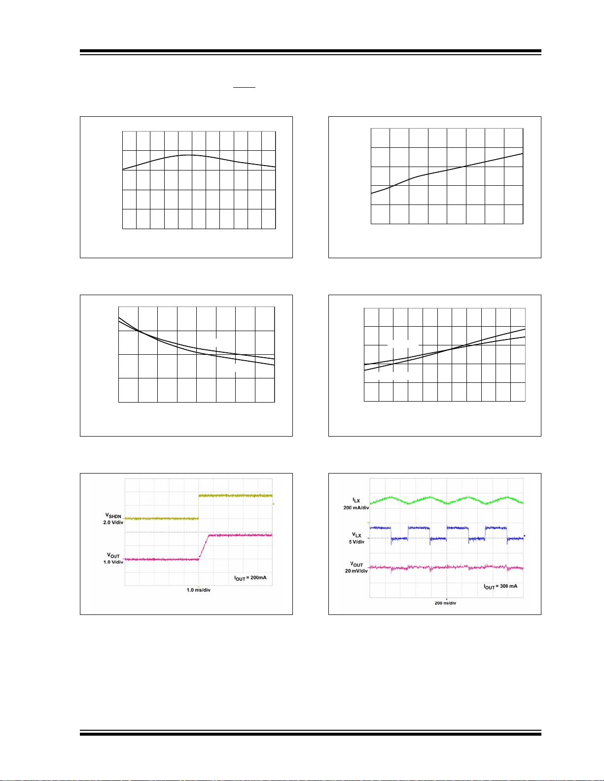
Typical Performance Curves (Continued)
Note: Unless otherwise indicated, VIN= SHDN =3.6V, C
T
= +25°C. Adjustable or fixed output voltage options can be used to generate the Typical Performance Characteristics.
A
OUT=CIN
= 4.7 µF, L = 4.7 µH, V
(ADJ) = 1.8V, I
OUT
LOAD
= 100 mA,
FIGURE 2-19: Light Load Switching Waveform.
FIGURE 2-20: Output Voltage Load Step Response vs. Time.
FIGURE 2-21: Output Voltage Line Step Response vs. Time.
FIGURE 2-22: Power-Good Output Timing.
DS22061A-page 10 © 2007 Microchip Technology Inc.

3.0 PIN DESCRIPTIONS
The descriptions of the pins are listed in Table 3-1.
TABLE 3-1: PIN FUNCTION TABLE
MSOP DFN Sym Description
MCP1602
1 1 SHDN
22VCCAnalog Input Supply Voltage Pin
3 3 PG Power Good Output Pin
44A
55V
66VINInput Supply Voltage Pin
77LXBuck Inductor Output Pin
88P
— Exposed
Pad
GND
FB/VOUT
GND
EP For the DFN package, the center exposed pad is a thermal path to remove
Shutdown Input Pin
Analog Ground Pin
Feedback Voltage (Adjustable Version) / Output Voltage (Fixed V ersion) Pin
Power Ground Pin
heat from the device. Electrically this pad is at ground potential and should
be connected to A
GND
3.1 Shutdown Control Input Pin
(SHDN
The SHDN pin is a logic-level input used to enable or
disable the device. A logic high (>45% of VIN) will
enable the regulator output. A logic-low (<15% of V
will ensure that the regulator is disabled.
)
)
IN
3.2 Analog Input Supply Voltage Pin
(V
)
CC
The VCC pin provides bias for internal analog functions.
This voltage is derived by filtering the VIN supply.
3.3 Power-Good Output Pin (PG)
PG is an output level indicating that the output voltage
is within 94% of regulation. The PG output is configured
as an open-drain output.
3.4 Analog Ground Pin (A
A
is the analog ground connection. Tie A
GND
analog portion of the ground plane (A
physical layout information in the Section 5.8 “PCB
Layout Information” section for ground recommendations.
GND
GND
)
to the
GND
). See the
3.6 Power Supply Input Voltage Pin
)
(V
IN
VIN is the buck regulator power input supply pin.
Connect a variable input voltage source to VIN.
3.7 Buck Inductor Output Pin (LX)
Connect LX directly to the buck inductor. This pin
carries large signal-level current; all connections
should be made as short as possible.
3.8 Power Ground Pin (P
Connect all large signal level ground returns to P
These large signal level ground traces should have a
small loop area and length to prevent coupling of
switching noise to sensitive traces.
GND
)
GND
3.9 Exposed Metal Pad (EP)
For the DFN package, connect the Exposed Pad to
, with vias into the A
A
GND
the A
package.
plane will aid in heat removal from the
GND
plane. This connection to
GND
.
3.5 Output Voltage Sense Pin (VFB/
V
)
OUT
For the adjustable output voltage options, connect the
center of the output voltage divider to the V
fixed-output voltage options, connect the output of the
buck regulator to this pin (V
© 2007 Microchip Technology Inc. DS22061A-page 11
OUT
).
pin. For
FB

MCP1602
V
TH_H
V
OUT
PG
t
RPU
t
RPD
V
OL
V
OH
V
TH_L
4.0 DETAILED DESCRIPTION
4.1 Device Overview
The MCP1602 is a synchronous buck regulator with a
power-good signal. The device operates in a Pulse
Frequency Modulation (PFM) mode or a Pulse Width
Modulation (PWM) mode to maximize system
efficiency over the entire operating current range.
Capable of operating from a 2.7V to 5.5V input voltage
source, the MCP1602 can deliver 500 mA of
continuous output current.
When using the MCP1602, the PCB area required for
a complete step-down converter is minimized since
both the main P-Channel MOSFET and the synchronous N-Channel MOSFET are integrated. Also while in
PWM mode, the device switches at a constant
frequency of 2.0 MHz (typical) which allow for small filtering components. Both fixed and adjustable output
voltage options are available. The fixed voltage options
(1.2V , 1.5V, 1.8V , 2.5V , 3.3V) do not require an external
voltage divider which further reduces the required
circuit board footprint. The adjustable output voltage
options allow for more flexibility in the design, but
require an external voltage divider.
Additionally the device features undervoltage lockout
(UVLO), overtemperature shutdown, overcurrent
protection, and enable/disable control.
4.2 Synchronous Buck Regulator
The MCP1602 has two distinct modes of operation that
allow the device to maintain a high level of efficiency
throughout the entire operating current and voltage
range. The device automatically switches between
PWM mode and PFM mode depending upon the output
load requirements.
4.2.1 FIXED FREQUENCY, PWM MODE
During heavy load conditions, the MCP1602 operates
at a high, fixed switching frequency of 2.0 MHz (typical). This minimizes output ripple (10 - 15 mV typically)
and noise while maintaining high efficiency (88% typical with V
= 3.6V, V
IN
During normal PWM operation, the beginning of a
switching cycle occurs when the internal P-Channel
MOSFET is turned on. The ramping inductor current is
sensed and tied to one input of the internal high-speed
comparator. The other input to the high-speed comparator is the error amplifier output. This is the difference
between the internal 0.8V reference and the sensed
output voltage. When the sensed current becomes
equal to the amplified error signal, the high-speed
comparator switches states and the P-Channel
MOSFET is turned off. The N-Channel MOSFET is
turned on until the internal oscillator sets an internal RS
latch initiating the beginning of another switching cycle.
OUT
= 1.8V, I
OUT
= 300 mA).
PFM-to-PWM mode transition is initiated for any of the
following conditions:
• Continuous device switching
• Output voltage has dropped out of regulation
4.2.2 LIGHT LOAD, PFM MODE
During light load conditions, the MCP1602 operates in
a PFM mode. When the MCP1602 enters this mode, it
begins to skip pulses to minimize unnecessary
quiescent current draw by reducing the number of
switching cycles per second. The typical quiescent
current draw for this device is 45 µA.
PWM-to-PFM mode transition is initiated for any of the
following conditions:
• Discontinuous inductor current is sensed for a set
duration
• Inductor peak current falls below the transition
threshold limit
4.3 Power-Good (PG)
The open-drain power-good (PG) circuitry monitors the
regulated output voltage. A fixed delay time of
approximately 262 ms is generated once the output
voltage is above the power-good high threshold,
, (typically 94% of V
V
TH_H
falls below the power-good low threshold, V
(typically 92% of V
OUT
low state indicating that the output is out of regulation.
The PG circuitry has a typical 165 µs delay when
detecting a falling output voltage. This helps to
increase the noise immunity of the power-good output,
avoiding false triggering of the PG signal during line
and load transients.
FIGURE 4-1: Power-Good Timing.
). As the output voltage
OUT
TH_L
) the PG signal transitions to a
,
DS22061A-page 12 © 2007 Microchip Technology Inc.

MCP1602
4.4 Soft Start
The output of the MCP1602 is controlled during startup. This control allows for a very minimal amount of
overshoot during start-up from VIN rising above
V
OUT
the UVLO voltage or SHDN being enabled.
4.5 Overtemperature Protection
Overtemperature protection circuitry is integrated in the
MCP1602. This circuitry monitors the device junction
temperature and shuts the device off if the junction temperature exceeds the typical 150
threshold is exceeded, the device will automatically
restart once the junction temperature drops by
approximately 10
overtemperture condition.
o
C. The soft start is reset during an
o
C threshold. If this
4.6 Overcurrent Protection
Cycle-by-cycle current limiting is used to protect the
MCP1602 from being damaged when an external short
circuit is applied. The typical peak current limit is
700 mA. If the sensed current reaches the 700 mA
limit, the P-Channel MOSFET is turned off, even if the
output voltage is not in regulation. The device will
attempt to start a new switching cycle when the internal
oscillator sets the internal RS latch.
4.7 Enable/Disable Control
The SHDN pin is used to enable or disable the
MCP1602. When the SHDN
device is disabled. When pulled high the device is
enabled and begins operation provided the input
voltage is not below the UVLO threshold or a fault
condition exists.
pin is pulled low, the
4.8 Undervoltage Lockout (UVLO)
The UVLO feature uses a comparator to sense the
input voltage (V
than the voltage necessary to properly operate the
MCP1602, the UVLO feature will hold the converter off.
When V
UVLO is released and soft start begins. Hysteresis is
built into the UVLO circuit to compensate for input
impedance. For example, if there is any resistance
between the input voltage source and the device when
it is operating, there will be a voltage drop at the input
to the device equal to I
is 200 mV.
rises above the necessary input voltage, the
IN
) level. If the input voltage is lower
IN
x RIN. The typical hysteresis
IN
© 2007 Microchip Technology Inc. DS22061A-page 13

MCP1602
R
BOT
R
TOP
V
FB
V
OUTVFB
–
---------------------------- -
⎝⎠
⎛⎞
×=
Example:
R
TOP
= 200 kΩ
V
OUT
=1.0V
V
FB
0.8V
R
BOT
= 200 kΩ x (0.8V/(1.0V - 0.8V))
R
BOT
= 800 kΩ
(Standard Value = 787 kΩ)
I
CIN RMS,
I
OUT MAX,
V
OUTVINVOUT
–()×
V
IN
----------------------------------------------------- -
⎝⎠
⎜⎟
⎛⎞
×=
ΔV
OUT
ΔILESR×
ΔI
L
8 fC××
-------------------- -+=
5.0 APPLICATION INFORMATION
5.1 Typical Applications
The MCP1602 synchronous buck regulator with powergood operates over a wide input voltage range
(2.7V to 5.5V) and is ideal for single-cell Li-Ion battery
powered applications, USB powered applications,
three cell NiMH or NiCd applications and 3V to 5V
regulated input applications.
5.2 Fixed Output Voltage Applications
The Typical Application Circuit shows a fixed
MCP1602 in a typical application used to convert three
NiMH batteries into a well regulated 1.5V @ 500 mA
output. A 4.7 µF input and output capacitor, a 4.7 µH
inductor, and a small RC filter make up the entire
external component selection for this application. No
external voltage divider or compensation is necessary.
In addition to the fixed 1.5V option, the MCP1602 is
also available in 1.2V, 1.8V, 2.5V, or 3.3V fixed voltage
options.
5.3 Adjustable Output Voltage Applications
For adjustable output applications, an additional R-C
compensation network is necessary for control loop
stability. Recommended valu es for any output voltage
are:
= 4.99 kΩ
R
COMP
= 33 pF
C
COMP
Refer to Figure 6-2 for proper placement of R
C
.
COMP
COMP
and
5.4 Input Capacitor Selection
The input current to a buck converter, when operating
in continuous conduction mode, is a squarewave with
a duty cycle defined by the output voltage (V
input voltage (VIN) relationship of V
undesirable input voltage transients, the input capacitor
should be a low ESR type with a RMS current rating
given by Equation 5-2. Because of their small size and
low ESR, ceramic capacitors are often used. Ceramic
material X5R or X7R are well suited since they have a
low temperature coefficient and acceptable ESR.
OUT/VIN
. To prevent
EQUATION 5-2:
OUT
) to
When the desired output for a particular application is
not covered by the fixed voltage options, an adjustable
MCP1602 can be used. The circuit listed in Figure 6-2
shows an adjustable MCP1602 being used to convert a
5V rail to 1.0V @ 500 mA. The output voltage is adjustable by using two external resistors as a voltage
divider. For adjustable output voltages, it is recommended that the top resistor divider value be 200 kΩ.
The bottom resistor value can be calculated using the
following equation.
EQUATION 5-1:
Table 5-1 contains the recommend range fo r the input
capacitor value.
5.5 Output Capacitor Selection
The output capacitor helps provide a stable output
voltage during sudden load transients, smooths the
current that flows from the inductor to the load, and it
also reduces the output voltage ripple. Therefore, low
ESR capacitors are a desirable choice for the output
capacitor. As with the input capacitor, X5R and X7R
ceramic capacitors are well suited for this application.
The output ripple voltage is often a design specification. A buck converters’ output ripple voltage is a
function of the charging and discharging of the output
capacitor and the ESR of the capacitor. This ripple
voltage can be calculated by Equation 5-3.
EQUATION 5-3:
DS22061A-page 14 © 2007 Microchip Technology Inc.

MCP1602
ΔI
L
V
OUT
F
SW
L×
-------------------
1
V
OUT
V
IN
-------------–
⎝⎠
⎛⎞
×=
Where:
F
SW
= Switching Frequency
V
OUTIOUT
×
Efficiency
-------------------------------
⎝⎠
⎛⎞
V
OUTIOUT
×()– P
Dis
=
Table 5-1 contains the recommend range for the output
capacitor value.
TABLE 5-1: CAPACITOR VALUE RANGE
C
IN
Minimum 4.7 µF 4.7 µF
Maximum — 22 µF
C
OUT
5.6 Inductor Selection
For most applications an inductor value of 4.7 µH is
recommended to achieve a good balance between
converter load transient response and minimized
noise. There are many different magnetic core
materials and package options to select from. That
decision is based on size, cost, and acceptable
radiated energy levels. Toroid and shielded ferrite pot
cores will have low radiated energy, but tend to be
larger and higher in cost.
The value of inductance is selected to achieve a
desired amount of ripple current. It is reasonable to
assume a ripple current that is 20% of the maximum
load current. The larger the amount of ripple current
allowed, the larger the output capa citor value become s
to meet ripple voltage specifications. The inductor
ripple current can be calculated according to
Equation 5-4.
EQUATION 5-4:
TABLE 5-2: MCP1602 RECOMMENDED
INDUCTORS (CONTINUED)
Part
Number
Wurth Elektronik®
WE-TPC
Type S
WE-TPC
Type S
WE-TPC
Type S
WE-TPC
Type M
WE-TPC
Type M
WE-TPC
Type M
Value
(µH)
3.6 0.085 1.10 3.8x3.8x1.65
4.7 0.105 0.90 3.8x3.8x1.65
6.8 0.156 0.75 3.8x3.8x1.65
3.3 0.065 1.80 4.8x4.8x1.8
4.7 0.082 1.65 4.8x4.8x1.8
6.8 0.100 1.25 4.8x4.8x1.8
DCR
Ω
(max)
I
SAT
(A)
Size
WxLxH (mm)
5.7 Thermal Calculations
The MCP1602 is available in two different packages
(MSOP and 3x3 DFN). By calculating the power
dissipation and applying the package thermal
resistance, (θ
estimated. The maximum continuous junction
temperature rating for the MCP1602 is +125
To quickly estimate the internal pow er dissipation for
the switching buck regulator, an empirical calculation
using measured efficiency can be used. Given the
measured efficiency, the internal power dissipation is
estimated by:
), the junction temperature is
JA
o
C.
When considering inductor ratings, the maximum DC
current rating of the inductor should be at least equal to
the maximum load current, plus one half the peak-topeak inductor ripple current (1/2 * ΔI
resistance adds to the total converter power loss. An
inductor with a low DC resistance allows for higher
converter efficiency.
TABLE 5-2: MCP1602 RECOMMENDED
Part
Number
Coiltronics®
SD10 3.3 0.108 1.31 5.2x5.2x1.0
SD10 4.7 0.154 1.08 5.2x5.2x1.0
SD10 6.2 0.218 0.92 5.2x5.2x1.0
SD12 3.3 0.104 1.42 5.2x5.2x1.2
SD12 4.7 0.118 1.29 5.2x5.2x1.2
SD12 6.2 0.170 1.08 5.2x5.2x1.2
© 2007 Microchip Technology Inc. DS22061A-page 15
INDUCTORS
Value
(µH)
(max)
DCR
Ω
). The inductor DC
L
I
SAT
(A)
Size
WxLxH (mm)
EQUATION 5-5:
The difference between the first term, input power
dissipation, and the second term, power delivered, is
the internal power dissipation. This is an estimate
assuming that most of the power lost is internal to the
MCP1602. There is some percentage of power lost in
the buck inductor, with very little loss in the input and
output capacitors.

MCP1602
SHDN
V
CC
PG
A
GND
V
FB
V
IN
L
X
P
GND
1
2
3
4
8
7
6
5
ON
OFF
MCP1602
V
IN
2.7V to 4.5V
V
OUT
1.5V @ 500 mA
V
IN
R
PULLUP
4.7 µF
4.7 µH
4.7 µF
0.1 µF
10Ω
Processor
Reset
5.8 PCB Layout Information
Good printed circuit board layout techniques are
important to any switching circuitry and switching
power supplies are no different. When wiring the high
current paths, short and wide traces should be used.
This high current path is shown with red connections in
Figure 5-1. Therefore, it is important that the
components along the high current path should be
placed as close as possible to the MCP1602 to
minimize the loop area.
The feedback resistors and feedback signal should be
routed away from the switching node and this switching
current loop. When possible ground planes and traces
should be used to help shield the feedback signal and
minimize noise and magnetic interference.
FIGURE 5-1: PCB High Current Path.
DS22061A-page 16 © 2007 Microchip Technology Inc.

6.0 TYPICAL APPLICATION CIRCUITS
SHDN
V
CC
PG
A
GND
V
FB
V
IN
L
X
P
GND
1
2
3
4
8
7
6
5
ON
OFF
MCP1602
V
IN
3.0V to 4.2V
V
OUT
1.5V @ 500 mA
V
IN
R
PULLUP
4.7 µF
4.7 µH
4.7 µF
0.1 µF
10Ω
Processor
Reset
SHDN
V
CC
PG
A
GND
V
OUT
V
IN
L
X
P
GND
1
2
3
4
8
7
6
5
ON
OFF
MCP1602
V
IN
5.0V
V
OUT
1.0V @ 500 mA
V
IN
R
PULLUP
4.7 µF
4.7 µH
4.7 µF
0.1 µF
10Ω
Processor
Reset
R
TOP
R
COMP
C
COMP
200 kΩ
R
BOT
787 kΩ
4.99 kΩ
33 pF
SHDN
V
CC
PG
A
GND
V
FB
V
IN
L
X
P
GND
1
2
3
4
8
7
6
5
ON
OFF
MCP1602
V
IN
2.7V to 4.5V
V
OUT
1.2V @ 500 mA
V
IN
R
PULLUP
4.7 µF
4.7 µH
4.7 µF
0.1 µF
10Ω
Processor
Reset
l
FIGURE 6-1: Single Li-Ion to 1.5V @ 500 mA Application.
MCP1602
FIGURE 6-2: 5V to 1.0V @ 500 mA Application.
FIGURE 6-3: 3 NiMH Batteries to 1.2V @ 500 mA Application.
© 2007 Microchip Technology Inc. DS22061A-page 17

MCP1602
Legend: XX...X Customer-specific information
Y Year code (last digit of calendar year)
YY Year code (last 2 digits of calendar year)
WW Week code (week of January 1 is week ‘01’)
NNN Alphanumeric traceability code
Pb-free JEDEC designator for Matte Tin (Sn)
* This package is Pb-free. The Pb-free JEDEC designator ( )
can be found on the outer packaging for this package.
Note: In the event the full Microchip part number cannot be marked on one line, it will
be carried over to the next line, thus limiting the number of available
characters for customer-specific information.
8-Lead MSOP Example:
8-Lead DFN (3x3)
Example
:
Part Number Code
MCP1602-120I/MF CAAU
MCP1602-150I/MF CAAV
MCP1602-180I/MF CAAW
MCP1602-250I/MF CAAY
MCP1602-330I/MF CAAZ
MCP1602-ADJI/MF CAAS
CAAU
0733
256
XXXX
XYWW
NNN
XXXXXX
YWWNNN
1602AJ
733256
Part Number Code
MCP1602-120I/MF 160212
MCP1602-150I/MF 160215
MCP1602-180I/MF 160218
MCP1602-250I/MF 160225
MCP1602-330I/MF 160233
MCP1602-ADJI/MF 1602AJ
7.0 PACKAGING INFORMATION
7.1 Package Marking Information
3
e
DS22061A-page 18 © 2007 Microchip Technology Inc.
3
e
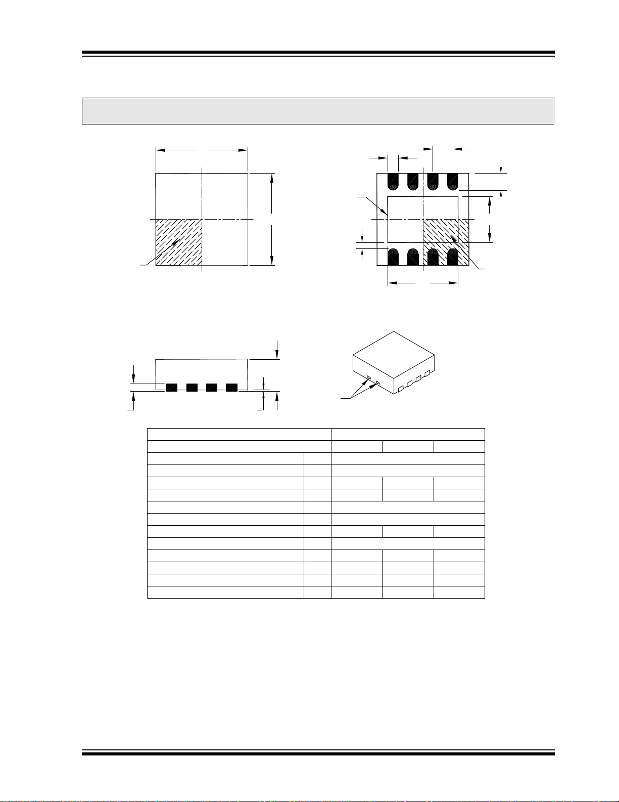
8-Lead Plastic Dual Flat, No Lead Package (MF) – 3x3x0.9 mm Body [DFN]
Notes:
1. Pin 1 visual index feature may vary, but must be located within the hatched area.
2. Package may have one or more exposed tie bars at ends.
3. Package is saw singulated.
4. Dimensioning and tolerancing per ASME Y14.5M.
BSC: Basic Dimension. Theoretically exact value shown without tolerances.
REF: Reference Dimension, usually without tolerance, for information purposes only.
Note: For the most current package drawings, please see the Microchip Packaging Specification located at
http://www.microchip.com/packaging
Units MILLIMETERS
Dimension Limits MIN NOM MAX
Number of Pins N 8
Pitch e 0.65 BSC
Overall Height A 0.80 0.90 1.00
Standoff A1 0.00 0.02 0.05
Contact Thickness A3 0.20 REF
Overall Length D 3.00 BSC
Exposed Pad Width E2 0.00 – 1.60
Overall Width E 3.00 BSC
Exposed Pad Length D2 0.00 – 2.40
Contact Width b 0.25 0.30 0.35
Contact Length L 0.20 0.30 0.55
Contact-to-Exposed Pad K 0.20 – –
BOTTOM VIEW
TOP VIEW
D
N
E
NOTE 1
12
EXPOSED PAD
b
e
N
L
E2
K
NOTE 1
D2
21
NOTE 2
A
A1
A3
Microchip Technology Drawing C04-062B
MCP1602
© 2007 Microchip Technology Inc. DS22061A-page 19
MCP1602
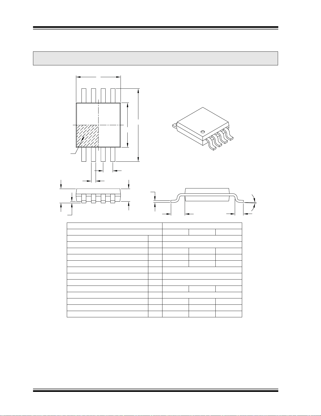
8-Lead Plastic Micro Small Outline Package (MS) [MSOP]
Notes:
1. Pin 1 visual index feature may vary, but must be located within the hatched area.
2. Dimensions D and E1 do not include mold flash or protrusions. Mold flash or protrusions shall not exceed 0.15 mm per side.
3. Dimensioning and tolerancing per ASME Y14.5M.
BSC: Basic Dimension. Theoretically exact value shown without tolerances.
REF: Reference Dimension, usually without tolerance, for information purposes only.
Note: For the most current package drawings, please see the Microchip Packaging Specification located at
http://www.microchip.com/packaging
Units MILLIMETERS
Dimension Limits MIN NOM MAX
Number of Pins N 8
Pitch e 0.65 BSC
Overall Height A – – 1.10
Molded Package Thickness A2 0.75 0.85 0.95
Standoff A1 0.00 – 0.15
Overall Width E 4.90 BSC
Molded Package Width E1 3.00 BSC
Overall Length D 3.00 BSC
Foot Length L 0.40 0.60 0.80
Footprint L1 0.95 REF
Foot Angle φ 0° – 8°
Lead Thickness c 0.08 – 0.23
Lead Width b 0.22 – 0.40
D
N
E
E1
NOTE 1
1
2
e
b
A
A1
A2
c
L1
L
φ
Microchip Technology Drawing C04-111B
DS22061A-page 20 © 2007 Microchip Technology Inc.

APPENDIX A: REVISION HISTORY
Revision A (October 2007)
• Original Release of this Document.
MCP1602
© 2007 Microchip Technology Inc. DS22061A-page 21

MCP1602
NOTES:
DS22061A-page 22 © 2007 Microchip Technology Inc.
PRODUCT IDENTIFICATION SYSTEM
Device MCP1602: 2.0 MHz, 500 mA, Buck Reg w/Power-Good
Tape & Reel T = Tape and Reel
Blank = Tube
Standard Fixed
Output Voltage * 120 = 1.20V
150 = 1.50V
180 = 1.80V
250 = 2.50V
330 = 3.30V
ADJ = Adjustable Voltage Version (0.8V to 4.5V)
* Custom output voltages available upon request. Contact
your local Microchip sales office for more information.
Temperature Range I = -40°C to +85°C
Package * MF = Plastic Dual Flat No Lead, (3x3 mm Body), 8-Lead
MS = Plastic Micro Small Outline, 8-Lead
PAR T NO. X XX
PackageTem p.
Device
Examples:
a) MCP1602-1202I/MF: 1.20V, 500 mA Buck
Reg, 8LD DFN Pkg.
b) MCP1602-1202I/MS: 1.20V, 500mA Buck
Reg, 8LD MSOP Pkg.
c) MCP1602-1502I/MF: 1.50V, 500 mA Buck
Reg, 8LD DFN Pkg.
d) MCP1602-1502I/MS: 1.50V, 500mA Buck
Reg, 8LD MSOP Pkg.
e) MCP1602-1802I/MF: 1.80V, 500 mA Buck
Reg, 8LD DFN Pkg.
f) MCP1602-1802I/MS: 1.80V, 500 mA Buck
Reg, 8LD MSOP Pkg.
g) MCP1602-2502I/MF: 2.50V, 500 mA Buck
Reg, 8LD DFN Pkg.
h) MCP1602-2502I/MS: 2.50V, 500mA Buck
Reg, 8LD MSOP Pkg.
i) MCP1602T-3302I/MF: Tape and Reel,
3.30V, 500 mA Buck
Reg, 8LD DFN Pkg.
j) MCP1602-3302I/MS: 3.30V, 500 mA Buck
Reg, 8LD MSOP Pkg.
k) MCP1602-ADJI/MF: Adjustable, 500 mA
Buck Reg, 8LD DFN
Pkg.
l) MCP1602-ADJI/MS: Adjustable, 500 mA
Buck Reg, 8LD MSOP
Pkg.
Range
-XX
X
Vol tag e
Output
X
Tap e &
Reel
To order or obtain information, e.g., on pricing or delivery, refer to the factory or the listed sales office.
MCP1602
© 2007 Microchip Technology Inc. DS22061A-page 23

MCP1602
NOTES:
DS22061A-page 24 © 2007 Microchip Technology Inc.
Note the following details of the code protection feature on Microchip devices:
• Microchip products meet the specification contained in their particular Microchip Data Sheet.
• Microchip believes that its family of products is one of the most secure families of its kind on the market today, when used in the
intended manner and under normal conditions.
• There are dishonest and possibly illegal methods used to breach the code protection feature. All of these methods, to our
knowledge, require using the Microchip products in a manner outside the operating specifications contained in Microchip’s Data
Sheets. Most likely, the person doing so is engaged in theft of intellectual property.
• Microchip is willing to work with the customer who is concerned about the integrity of their code.
• Neither Microchip nor any other semiconductor manufacturer can guarantee the security of their code. Code protection does not
mean that we are guaranteeing the product as “unbreakable.”
Code protection is constantly evolving. We at Microchip are committed to continuously improving the code protection features of our
products. Attempts to break Microchip’s code protection feature may be a violation of the Digital Millennium Copyright Act. If such acts
allow unauthorized access to your software or other copyrighted work, you may have a right to sue for relief under that Act.
Information contained in this publication regarding device
applications and the like is provided only for your convenience
and may be superseded by updates. It is your responsibility to
ensure that your application meets with your specifications.
MICROCHIP MAKES NO REPRESENTATIONS OR
WARRANTIES OF ANY KIND WHETHER EXPRESS OR
IMPLIED, WRITTEN OR ORAL, STATUTORY OR
OTHERWISE, RELATED TO THE INFORMATION,
INCLUDING BUT NOT LIMITED TO ITS CONDITION,
QUALITY, PERFORMANCE, MERCHANTABILITY OR
FITNESS FOR PURPOSE. Microchip disclaims all liability
arising from this information and its use. Use of Microchip
devices in life support and/or safety applications is entirely at
the buyer’s risk, and the buyer agrees to defend, indemnify and
hold harmless Microchip from any and all damages, claims,
suits, or expenses resulting from such use. No licenses are
conveyed, implicitly or otherwise, under any Microchip
intellectual property rights.
Trademarks
The Microchip name and logo, the Microchip logo, Accuron,
dsPIC, K
EELOQ, KEELOQ logo, microID, MPLAB, PIC,
PICmicro, PICSTART, PRO MATE, rfPIC and SmartShunt are
registered trademarks of Microchip Technology Incorporated
in the U.S.A. and other countries.
AmpLab, FilterLab, Linear Active Thermistor, Migratable
Memory, MXDEV, MXLAB, SEEVAL, SmartSensor and The
Embedded Control Solutions Company are registered
trademarks of Microchip Technology Incorporated in the
U.S.A.
Analog-for-the-Digital Age, Application Maestro, CodeGuard,
dsPICDEM, dsPICDEM.net, dsPICworks, dsSPEAK, ECAN,
ECONOMONITOR, FanSense, FlexROM, fuzzyLAB,
In-Circuit Serial Programming, ICSP, ICEPIC, Mindi, MiWi,
MPASM, MPLAB Certified logo, MPLIB, MPLINK, PICkit,
PICDEM, PICDEM.net, PICLAB, PICtail, PowerCal,
PowerInfo, PowerMate, PowerTool, REAL ICE, rfLAB, Select
Mode, Smart Serial, SmartTel, Total Endurance, UNI/O,
WiperLock and ZENA are trademarks of Microchip
Technology Incorporated in the U.S.A. and other countries.
SQTP is a service mark of Microchip Technology Incorporated
in the U.S.A.
All other trademarks mentioned herein are property of their
respective companies.
© 2007, Microchip Technology Incorporated, Printed in the
U.S.A., All Rights Reserved.
Printed on recycled paper.
Microchip received ISO/TS-16949:2002 certification for its worldwide
headquarters, design and wafer fabrication facilities in Chandler and
T empe, Arizona; Gresham, Oregon and design centers in California
and India. The Company’s quality system processes and procedures
are for its PIC
devices, Serial EEPROMs, microperipherals, nonvolatile memory and
analog products. In addition, Microchip’s quality system for the desig n
and manufacture of development systems is ISO 9001:2000 certified.
®
MCUs and dsPIC® DSCs, KEELOQ
®
code hopping
© 2007 Microchip Technology Inc. DS22061A-page 25

WORLDWIDE SALES AND SERVICE
AMERICAS
Corporate Office
2355 West Chandler Blvd.
Chandler, AZ 85224-6199
Tel: 480-792-7200
Fax: 480-792-7277
Technical Support:
http://support.microchip.com
Web Address:
www.microchip.com
Atlanta
Duluth, GA
Tel: 678-957-9614
Fax: 678-957-1455
Boston
Westborough, MA
Tel: 774-760-0087
Fax: 774-760-0088
Chicago
Itasca, IL
Tel: 630-285-0071
Fax: 630-285-0075
Dallas
Addison, TX
Tel: 972-818-7423
Fax: 972-818-2924
Detroit
Farmington Hills, MI
Tel: 248-538-2250
Fax: 248-538-2260
Kokomo
Kokomo, IN
Tel: 765-864-8360
Fax: 765-864-8387
Los Angeles
Mission Viejo, CA
Tel: 949-462-9523
Fax: 949-462-9608
Santa Clara
Santa Clara, CA
Tel: 408-961-6444
Fax: 408-961-6445
Toronto
Mississauga, Ontario,
Canada
Tel: 905-673-0699
Fax: 905-673-6509
ASIA/PACIFIC
Asia Pacific Office
Suites 3707-14, 37th Floor
Tower 6, The Gateway
Harbour City, Kowloon
Hong Kong
Tel: 852-2401-1200
Fax: 852-2401-3431
Australia - Sydney
Tel: 61-2-9868-6733
Fax: 61-2-9868-6755
China - Beijing
Tel: 86-10-8528-2100
Fax: 86-10-8528-2104
China - Chengdu
Tel: 86-28-8665-5511
Fax: 86-28-8665-7889
China - Fuzhou
Tel: 86-591-8750-3506
Fax: 86-591-8750-3521
China - Hong Kong SAR
Tel: 852-2401-1200
Fax: 852-2401-3431
China - Nanjing
Tel: 86-25-8473-2460
Fax: 86-25-8473-2470
China - Qingdao
Tel: 86-532-8502-7355
Fax: 86-532-8502-7205
China - Shanghai
Tel: 86-21-5407-5533
Fax: 86-21-5407-5066
China - Shenyang
Tel: 86-24-2334-2829
Fax: 86-24-2334-2393
China - Shenzhen
Tel: 86-755-8203-2660
Fax: 86-755-8203-1760
China - Shunde
Tel: 86-757-2839-5507
Fax: 86-757-2839-5571
China - Wuhan
Tel: 86-27-5980-5300
Fax: 86-27-5980-5118
China - Xian
Tel: 86-29-8833-7252
Fax: 86-29-8833-7256
ASIA/PACIFIC
India - Bangalore
Tel: 91-80-4182-8400
Fax: 91-80-4182-8422
India - New Delhi
Tel: 91-11-4160-8631
Fax: 91-11-4160-8632
India - Pune
Tel: 91-20-2566-1512
Fax: 91-20-2566-1513
Japan - Yokohama
Tel: 81-45-471- 6166
Fax: 81-45-471-6122
Korea - Daegu
Tel: 82-53-744-4301
Fax: 82-53-744-4302
Korea - Seoul
Tel: 82-2-554-7200
Fax: 82-2-558-5932 or
82-2-558-5934
Malaysia - Kuala Lumpur
Tel: 60-3-6201-9857
Fax: 60-3-6201-9859
Malaysia - Penang
Tel: 60-4-227-8870
Fax: 60-4-227-4068
Philippines - Manila
Tel: 63-2-634-9065
Fax: 63-2-634-9069
Singapore
Tel: 65-6334-8870
Fax: 65-6334-8850
Taiwan - Hsin Chu
Tel: 886-3-572-9526
Fax: 886-3-572-6459
Taiwan - Kaohsiung
Tel: 886-7-536-4818
Fax: 886-7-536-4803
Taiwan - Taipei
Tel: 886-2-2500-6610
Fax: 886-2-2508-0102
Thailand - Bangkok
Tel: 66-2-694-1351
Fax: 66-2-694-1350
EUROPE
Austria - Wels
Tel: 43-7242-2244-39
Fax: 43-7242-2244-393
Denmark - Copenhagen
Tel: 45-4450-2828
Fax: 45-4485-2829
France - Paris
Tel: 33-1-69-53-63-20
Fax: 33-1-69-30-90-79
Germany - Munich
Tel: 49-89-627-144-0
Fax: 49-89-627-144-44
Italy - Milan
Tel: 39-0331-742611
Fax: 39-0331-466781
Netherlands - Drunen
Tel: 31-416-690399
Fax: 31-416-690340
Spain - Madrid
Tel: 34-91-708-08-90
Fax: 34-91-708-08-91
UK - Wokingham
Tel: 44-118-921-5869
Fax: 44-118-921-5820
10/05/07
DS22061A-page 26 © 2007 Microchip Technology Inc.
 Loading...