

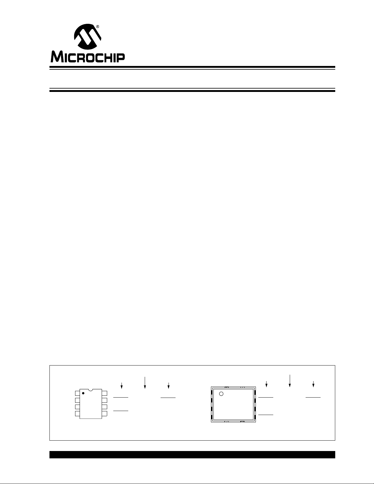
MCP14E3/MCP14E4/MCP14E5
ENB_A
IN A
GND
IN B
8-Pin
1
2
3
4
ENB_B
5
6
7
8
OUT A
OUT B
ENB_A
IN A
GND
IN B
V
DD
Note 1: Exposed pad of the DFN package is electrically isolated.
MCP14E3
MCP14E4
ENB_B
OUT A
OUT B
V
DD
MCP14E5
ENB_B
OUT A
OUT B
V
DD
ENB_B
OUT A
OUT B
V
DD
MCP14E3
MCP14E4
ENB_B
OUT A
OUT B
V
DD
MCP14E5
ENB_B
OUT A
OUT B
V
DD
PDIP/SOIC
8-Pin
6x5 DFN
(1)
1
2
3
4
5
6
7
8
4.0A Dual High-Speed Power MOSFET Drivers With Enable
Features
• High Peak Output Current: 4.0A (typical)
• Independent Enable Function for Each Driver
Output
• Low Shoot-Through/Cross-Conduction Current in
Output Stage
• Wide Input Supply Voltage Operating Range:
- 4.5V to 18V
• High Capacitive Load Drive Capability:
- 2200 pF in 15 ns (typical)
- 5600 pF in 26 ns (typical)
• Short Delay Times: 50 ns (typical)
• Latch-Up Protected: Will Withstand 1.5A Reverse
Current
• Logic Input Will Withstand Negative Swing Up To
5V
• Space-Saving Packages:
- 8-Lead 6x5 DFN, PDIP, SOIC
Applications
• Switch Mode Power Supplies
• Pulse Transformer Drive
• Line Drivers
• Motor and Solenoid Drive
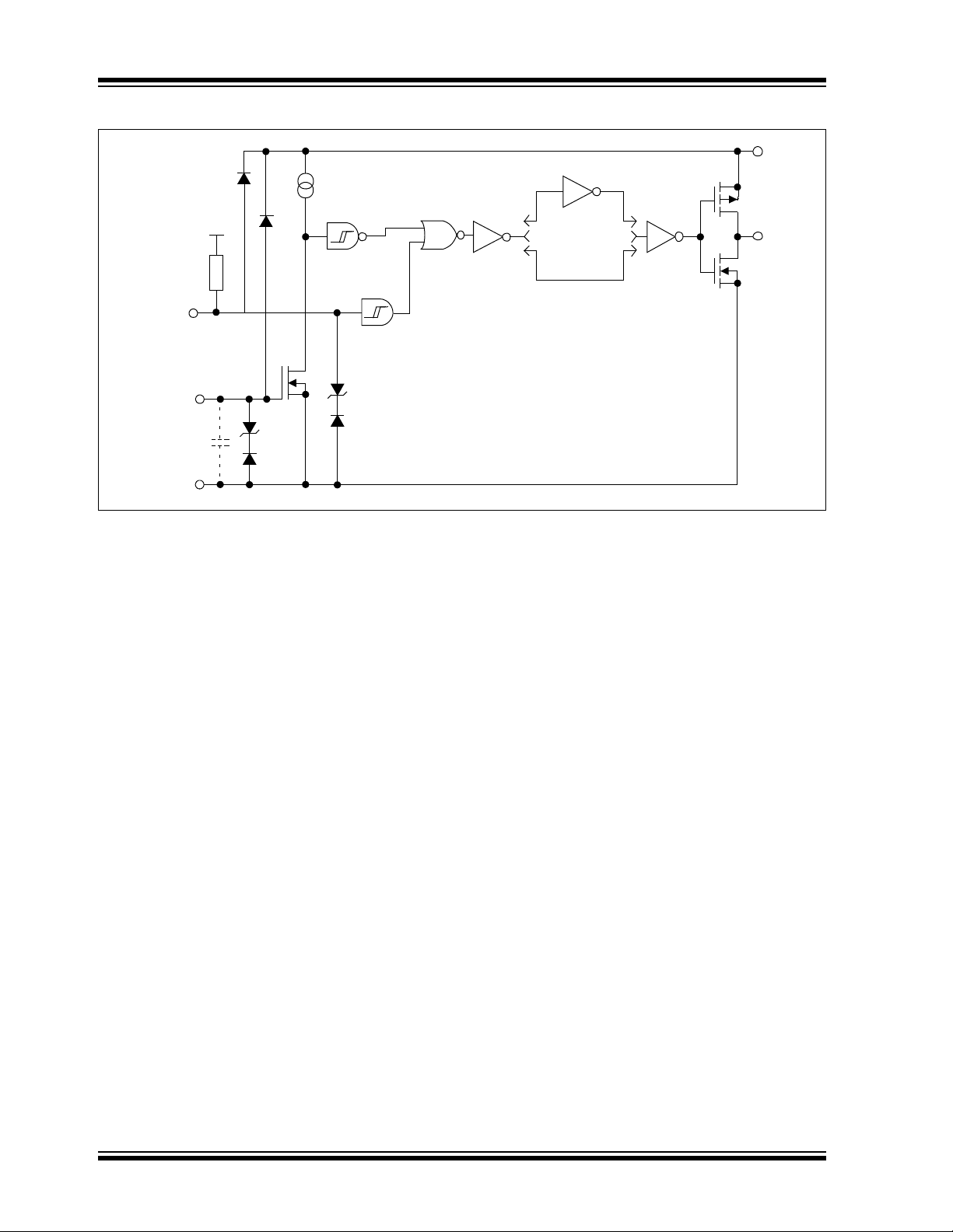
General Description
The MCP14E3/MCP14E4/MCP14E5 devices are a
family of 4.0A buffers/MOSFET drivers. Dual-inverting,
dual-noninvertering, and complementary outputs are
standard logic options offered.
The MCP14E3/MCP14E4/MCP14E5 drivers are
capable of operating from a 4.5V to 18V single power
supply and can easily charge and discharge 2200 pF
gate capacitance in under 15 ns (typical). They provide
low impedance in both the ON and OFF states to
ensure the MOSFET’s intended state will not be
affected, even by large transients. The MCP14E3/
MCP14E4/MCP14E5 inputs may be driven directly
from either TTL or CMOS (2.4V to 18V).
Additional control of the MCP14E3/MCP14E4/
MCP14E5 outputs is allowed by the use of separate
enable functions. The ENB_A and ENB_B pins are
active high and are internally pulled up to V
maybe left floating for standard operation.
The MCP14E3/MCP14E4/MCP14E5 dual-output 4.0A
driver family is offered in both surface-mount and pinthrough-hole packages with a -40°C to +125°C
temperature rating. The low thermal resistance of the
thermally enhanced DFN package allows for greater
power dissipation capability for driving heavier
capacitive or resistive loads.
These devices are highly latch-up resistant under any
conditions within their power and voltage ratings. They
are not subject to damage when up to 5V of noise
spiking (of either polarity) occurs on the ground pin.
They can accept, without damage or logic upset, up to
1.5A of reverse current being forced back into their
outputs. All terminals are fully protect against
Electrostatic Discharge (ESD) up to 4 kV.
. The pins
DD
Package Types
© 2007 Microchip Technology Inc. DS22062A-page 1
MCP14E3/MCP14E4/MCP14E5
Effective
Input C = 20 pF
(Each Input)
MCP14E3
MCP14E4
MCP14E5
Dual Inverting
Dual Noninverting
One Inverting, One Noninverting
Output
Input
GND
V
DD
4.7 V
Inverting
Non-inverting
Enable
V
DD
Internal
Pull-up
4.7 V
Functional Block Diagram
DS22062A-page 2 © 2007 Microchip Technology Inc.
MCP14E3/MCP14E4/MCP14E5
1.0 ELECTRICAL
CHARACTERISTICS
Absolute Maximum Ratings †
Supply Voltage................................................................+20V
Input Voltage...............................(V
Enable Voltage.............................(V
Input Current (V
Package Power Dissipation (T
8L-DFN ....................................................................... Note 3
8L-PDIP ........................................................................1.10W
8L-SOIC ..................................................................... 665 mW
)................................................50 mA
IN>VDD
+ 0.3V) to (GND – 5V)
DD
+ 0.3V) to (GND - 5V)
DD
= 50°C)
A
† Notice: Stresses above those listed under "Maximum
Ratings" may cause permanent damage to the device. This is
a stress rating only and functional operation of the device at
those or any other conditions above those indicated in the
operational sections of this specification is not intended.
Exposure to maximum rating conditions for extended periods
may affect device reliability.
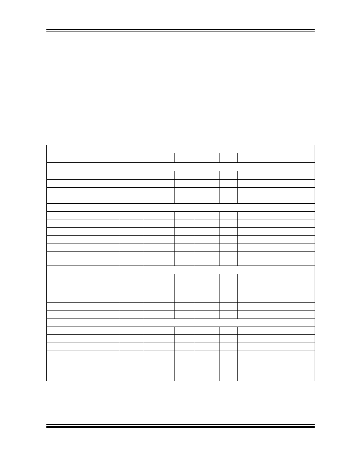
DC CHARACTERISTICS (NOTE 2)
Electrical Specifications: Unless otherwise indicated, TA = +25°C, with 4.5V ≤ VDD ≤ 18V.
Parameters Sym Min Typ Max Units Conditions
Input
Logic ‘1’, High Input Voltage V
Logic ‘0’, Low Input Voltage V
Input Current I
Input Voltage V
IH
IL
IN
IN
Output
High Output Voltage V
Low Output Voltage V
Output Resistance, High R
Output Resistance, Low R
Peak Output Current I
Latch-Up Protection With-
I
REV
OH
OL
OH
OL
PK
stand Reverse Current
Switching Time (Note 1)
Rise Time t
Fall Time t
Propagation Delay Time t
Propagation Delay Time t
R
F
D1
D2
Enable Function (ENB_A, ENB_B)
High-Level Input Voltage V
Low-Level Input Voltage V
Hysteresis V
Enable Leakage Current I
Propagation Delay Time t
Propagation Delay Time t
EN_H
EN_L
HYST
ENBL
D3
D4
Note 1: Switching times ensured by design.
2: Tested during characterization, not production tested.
3: Package power dissipation is dependent on the copper pad area on the PCB.
2.4 1.5 — V
—1.30.8V
–1 — 1 µA 0V ≤ VIN ≤ V
-5 — VDD+0.3 V
VDD – 0.025 — — V DC Test
— — 0.025 V DC Test
—2.53.5Ω I
—2.53.0Ω I
—4.0—AV
OUT
OUT
DD
— >1.5 — A Duty cycle ≤ 2%, t ≤ 300 µs
—1530nsFigure 4-1, Figure 4-2
= 2200 pF
C
L
—1830nsFigure 4-1, Figure 4-2
CL = 2200 pF
—4655nsFigure 4-1, Figure 4-2
—5055nsFigure 4-1, Figure 4-2
1.60 1.90 2.90 V VDD= 12V, LO to HI Transition
1.30 2.20 2.40 V VDD= 12V, HI to LO Transition
0.10 0.30 0.60 V
40 85 115 µA VDD=12V,
ENB_A = ENB_B = GND
—60—nsFigure 4-3 (Note 1)
—50—nsFigure 4-3 (Note 1)
DD
= 10 mA, VDD = 18V
= 10 mA, VDD = 18V
= 18V (Note 2)
© 2007 Microchip Technology Inc. DS22062A-page 3
MCP14E3/MCP14E4/MCP14E5
DC CHARACTERISTICS (NOTE 2) (CONTINUED)
Electrical Specifications: Unless otherwise indicated, TA = +25°C, with 4.5V ≤ VDD ≤ 18V.
Parameters Sym Min Typ Max Units Conditions
Power Supply
Supply Voltage V
Supply Current I
DD
DD
I
DD
I
DD
I
DD
I
DD
I
DD
I
DD
I
DD
Note 1: Switching times ensured by design.
2: Tested during characterization, not production tested.
3: Package power dissipation is dependent on the copper pad area on the PCB.
4.5 — 18.0 V
—1.602.00mAV
IN_A
ENB_A = ENB_B = High
—0.600.90mAV
IN_A
ENB_A = ENB_B = High
—1.201.40mAV
IN_A
ENB_A = ENB_B = High
—1.201.40mAV
IN_A
ENB_A = ENB_B = High
—1.401.80mAV
IN_A
ENB_A = ENB_B = Low
—0.550.75mAV
IN_A
ENB_A = ENB_B = Low
—1.001.20mAV
IN_A
ENB_A = ENB_B = Low
—1.001.20mAV
IN_A
ENB_A = ENB_B = Low
=3V, V
=0V, V
=3V, V
=0V, V
=3V, V
=0V, V
=3V, V
=0V, V
IN_B
IN_B
IN_B
IN_B
IN_B
IN_B
IN_B
IN_B
=3V,
=0V,
=0V,
=3V,
=3V,
=0V,
=0V,
=3V,
DS22062A-page 4 © 2007 Microchip Technology Inc.
MCP14E3/MCP14E4/MCP14E5
DC CHARACTERISTICS (OVER OPERATING TEMPERATURE RANGE)
Electrical Specifications: Unless otherwise indicated, operating temperature range with 4.5V ≤ VDD ≤ 18V.
Parameters Sym Min Typ Max Units Conditions
Input
Logic ‘1’, High Input Voltage V
Logic ‘0’, Low Input Voltage V
Input Current I
IH
IL
IN
Output
High Output Voltage V
Low Output Voltage V
Output Resistance, High R
Output Resistance, Low R
OHVDD
OL
OH
OL
Switching Time (Note 1)
Rise Time t
Fall Time t
Delay Time t
Delay Time t
R
F
D1
D2
Enable Function (ENB_A, ENB_B)
High-Level Input Voltage V
Low-Level Input Voltage V
Hysteresis V
Enable Leakage Current I
Propagation Delay Time t
Propagation Delay Time t
EN_H
EN_L
HYST
ENBL
D3
D4
Power Supply
Supply Voltage V
Supply Current I
DD
DD
I
DD
I
DD
I
DD
I
DD
I
DD
I
DD
I
DD
Note 1: Switching times ensured by design.
2.4 — — V
——0.8V
–10 — +10 µA 0V ≤ VIN ≤ V
DD
– 0.025 — — V DC TEST
— — 0.025 V DC TEST
—3.06.0Ω I
—3.05.0Ω I
= 10 mA, VDD = 18V
OUT
= 10 mA, VDD = 18V
OUT
—2540nsFigure 4-1, Figure 4-2
CL = 2200 pF
—2840nsFigure 4-1, Figure 4-2
CL = 2200 pF
—5070nsFigure 4-1, Figure 4-2
—5070nsFigure 4-1, Figure 4-2
1.60 2.20 2.90 V VDD= 12V, LO to HI Transition
1.30 1.80 2.40 V VDD= 12V, HI to LO Transition
—0.40—V
40 87 115 µA VDD= 12V, ENB_A = ENB_B = GND
—50—nsFigure 4-3
—60—nsFigure 4-3
4.5 — 18.0 V
—2.03.0mAV
IN_A
=3V, V
IN_B
=3V,
ENB_A = ENB_B = High
—0.81.1mAV
IN_A
=0V, V
IN_B
=0V,
ENB_A = ENB_B = High
—1.52.0mAV
IN_A
=3V, V
IN_B
=0V,
ENB_A = ENB_B = High
—1.52.0mAV
IN_A
=0V, V
IN_B
=3V,
ENB_A = ENB_B = High
—1.82.8mAV
IN_A
=3V, V
IN_B
=3V,
ENB_A = ENB_B = Low
—0.60.8mAV
IN_A
=0V, V
IN_B
=0V,
ENB_A = ENB_B = Low
—1.11.8mAV
IN_A
=3V, V
IN_B
=0V,
ENB_A = ENB_B = Low
—1.11.8mAV
IN_A
=0V, V
IN_B
=3V,
ENB_A = ENB_B = Low
© 2007 Microchip Technology Inc. DS22062A-page 5
MCP14E3/MCP14E4/MCP14E5
TEMPERATURE CHARACTERISTICS
Electrical Specifications: Unless otherwise noted, all parameters apply with 4.5V ≤ VDD ≤ 18V.
Parameters Sym Min Typ Max Units Conditions
Temperature Ranges
Specified Temperature Range T
Maximum Junction Temperature T
Storage Temperature Range T
Package Thermal Resistances
Thermal Resistance, 8L-6x5 DFN θ
Thermal Resistance, 8L-PDIP θ
Thermal Resistance, 8L-SOIC θ
A
A
JA
JA
JA
–40 — +125 °C
J
— — +150 °C
–65 — +150 °C
— 35.7 — °C/W Typical four-layer board with
vias to ground plane
—89.3 —°C/W
— 149.5 — °C/W
DS22062A-page 6 © 2007 Microchip Technology Inc.
MCP14E3/MCP14E4/MCP14E5
0
20
40
60
80
100
4 6 8 10 12 14 16 18
Supply Voltage (V)
Rise Time (ns)
10,000 pF
6,800 pF
4,700 pF
2,200 pF
100 pF
0
10
20
30
40
50
60
100 1000 10000
Capacitive Load (pF)
Rise Time (ns)
5V
12V
18V
10
12
14
16
18
20
22
24
-40 -25 -10 5 20 35 50 65 80 95 110 125
Temperature (°C)
Time (ns)
VDD = 18V
t
RISE
t
FALL
0
30
60
90
120
4 6 8 1012141618
Supply Voltage (V)
Fall Time (ns)
10,000 pF
6,800 pF
4,700 pF
2,200 pF
100 pF
0
10
20
30
40
50
60
100 1000 10000
Capacitive Load (pF)
Fall Time (ns)
5V
12V
18V
35
40
45
50
55
60
4 5 6 7 8 9 10 11 12
Input Amplitude (V)
Propagation Delay (ns)
VDD = 12V
t
D1
t
D2
2.0 TYPICAL PERFORMANCE CURVES
Note: The graphs and tables provided following this note are a statistical summary based on a limited number of
samples and are provided for informational purposes only. The performance characteristics listed herein are
not tested or guaranteed. In some graphs or tables, the data presented may be outside the specified
operating range (e.g., outside specified power supply range) and therefore outside the warranted range.
Note: Unless otherwise indicated, TA = +25C with 4.5V ≤ VDD ≤ 18V.
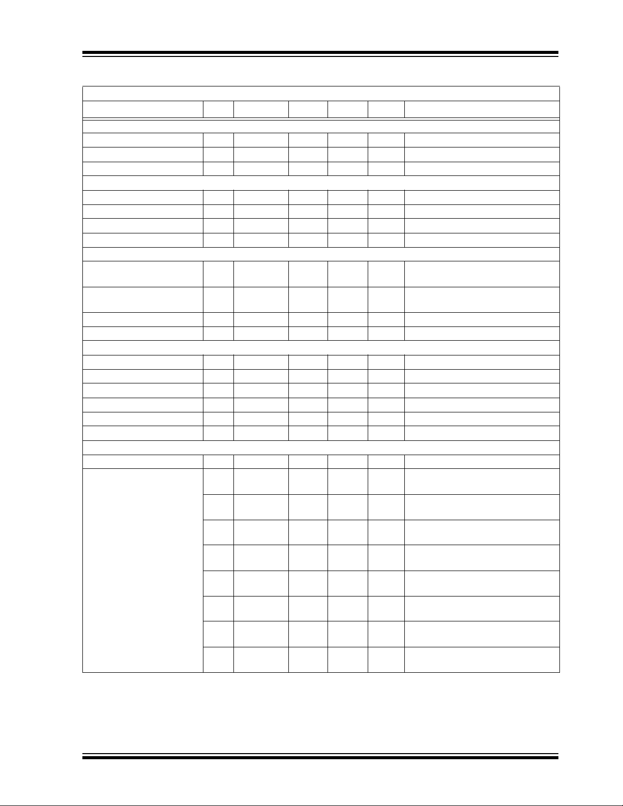
FIGURE 2-1: Rise Time vs. Supply Voltage.
FIGURE 2-2: Rise Time vs. Capacitive Load.
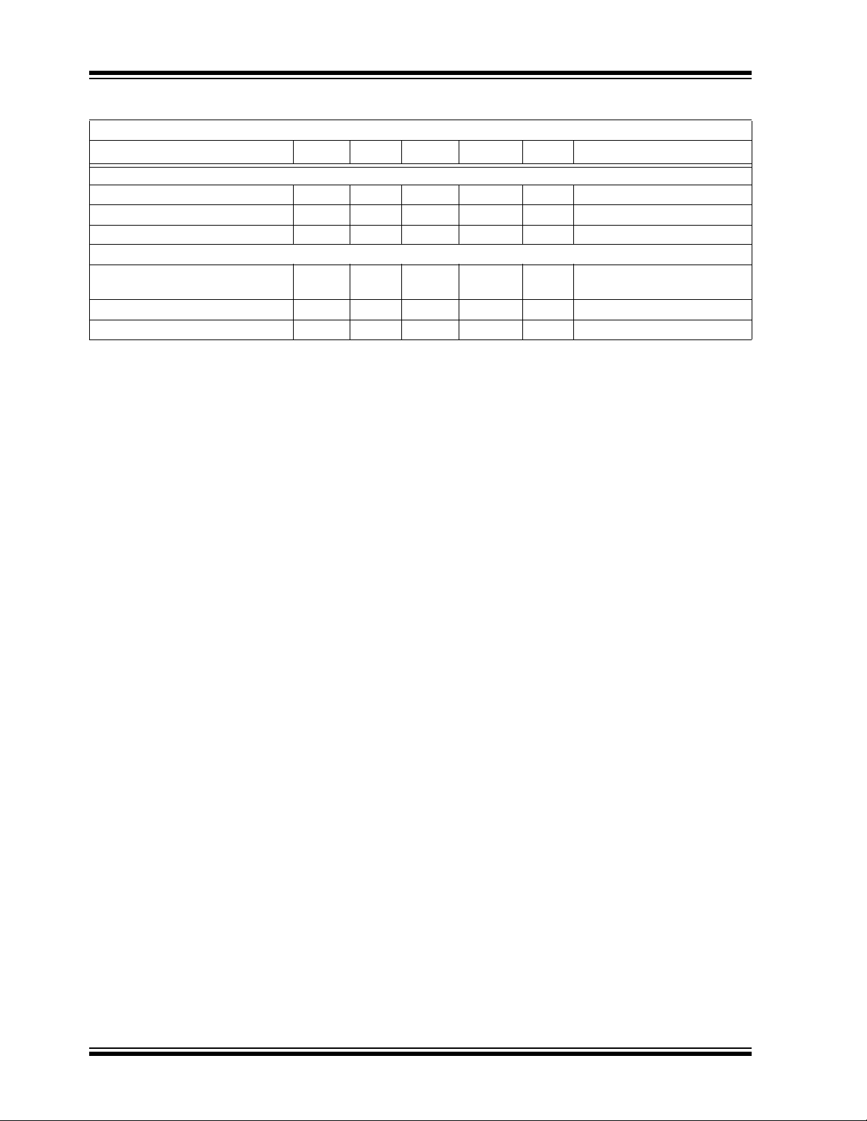
FIGURE 2-4: Fall Time vs. Supply Voltage.
FIGURE 2-5: Fall Time vs. Capacitive Load.
FIGURE 2-3: Rise and Fall Times vs. Temperature.
© 2007 Microchip Technology Inc. DS22062A-page 7
FIGURE 2-6: Propagation Delay vs. Input Amplitude.
MCP14E3/MCP14E4/MCP14E5
20
40
60
80
100
120
140
4 6 8 10 12 14 16 18
Supply Voltage (V)
Propagation Delay (ns)
t
D1
t
D2
0.0
0.2
0.4
0.6
0.8
1.0
1.2
1.4
4 6 8 1012141618
Supply Voltage (V)
Quiescent Current (mA)
Input = 1
Input = 0
1
2
3
4
5
6
7
8
4 6 8 1012141618
Supply Voltage (V)
R
OUT-HI
(Ω)
TA = 125°C
TA = 25°C
VIN = 0V (MCP14E3)
V
IN
= 5V (MCP14E4)
40
50
60
70
80
-40 -25 -10 5 20 35 50 65 80 95 110 125
Temperature (°C)
Propagatin Delay (ns)
t
D1
t
D2
VDD = 12V
0.2
0.4
0.6
0.8
1.0
1.2
1.4
1.6
1.8
-40 -25 -10 5 20 35 50 65 80 95 110 125
Temperature (°C)
Quiescent Current (mA)
Input = 1
Input = 0
VDD = 18V
1
2
3
4
5
6
7
8
4 6 8 1012141618
Supply Voltage (V)
R
OUT-LO
(Ω)
TA = 125°C
TA = 25°C
VIN = 5V (MCP14E3)
V
IN
= 0V (MCP14E4)
Typical Performance Curves (Continued)
Note: Unless otherwise indicated, TA = +25C with 4.5V ≤ VDD ≤ 18V.
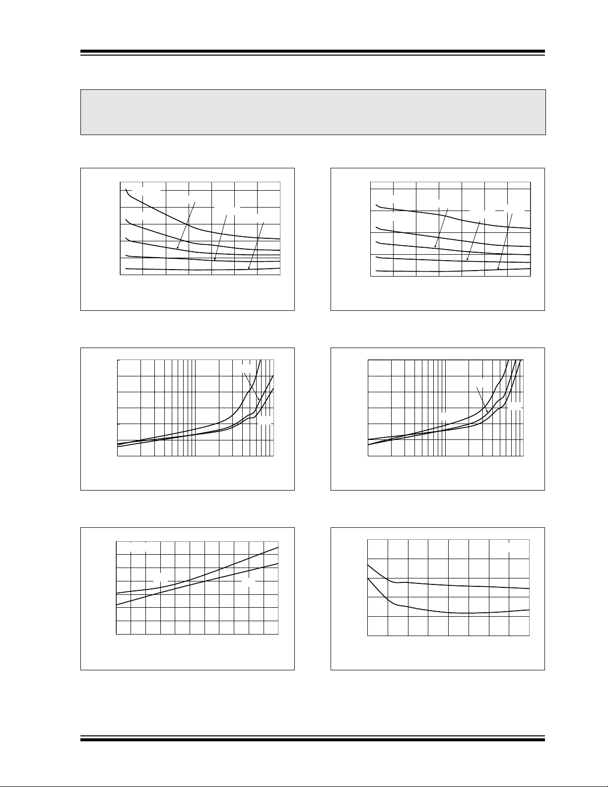
FIGURE 2-7: Propagation Delay Time vs. Supply Voltage.
FIGURE 2-8: Quiescent Current vs. Supply Voltage.
FIGURE 2-10: Propagation Delay Time vs. Temperature.
FIGURE 2-11: Quiescent Current vs. Temperature.
FIGURE 2-9: Output Resistance (Output High) vs. Supply Voltage.
DS22062A-page 8 © 2007 Microchip Technology Inc.
FIGURE 2-12: Output Resistance (Output Low) vs. Supply Voltage.
MCP14E3/MCP14E4/MCP14E5
0
20
40
60
80
100
120
100 1000 10000
Capacitive Load (pF)
Supply Current (mA)
650 kHz
400 kHz 200 kHz
100 kHz
50 kHz
VDD = 18V
0
10
20
30
40
50
60
70
100 1000 10000
Capacitive Load (pF)
Supply Current (mA)
650 kHz
400 kHz 200 kHz
100 kHz
50 kHz
VDD = 12V
0
5
10
15
20
25
30
35
100 1000 10000
Capacitive Load (pF)
Supply Current (mA)
650 kHz
400 kHz 200 kHz
100 kHz
50 kHz
VDD = 6V
0
20
40
60
80
100
120
10 100 1000
Frequency (kHz)
Supply Current (mA)
10,000 pF
6,800 pF
4,700 pF
2,200 pF
100 pF
VDD = 18V
0
10
20
30
40
50
60
70
10 100 1000
Frequency (kHz)
Supply Current (mA)
10,000 pF
6,800 pF
4,700 pF
2,200 pF
100 pF
VDD = 12V
0
5
10
15
20
25
30
35
10 100 1000
Frequency (kHz)
Supply Current (mA)
10,000 pF
6,800 pF
4,700 pF
2,200 pF
100 pF
VDD = 6V
Typical Performance Curves (Continued)
Note: Unless otherwise indicated, TA = +25C with 4.5V ≤ VDD ≤ 18V.
FIGURE 2-13: Supply Current vs. Capacitive Load.
FIGURE 2-14: Supply Current vs. Capacitive Load.
FIGURE 2-16: Supply Current vs. Frequency.
FIGURE 2-17: Supply Current vs. Frequency.
FIGURE 2-15: Supply Current vs. Capacitive Load.
© 2007 Microchip Technology Inc. DS22062A-page 9
FIGURE 2-18: Supply Current vs. Frequency.

MCP14E3/MCP14E4/MCP14E5
0.7
0.9
1.1
1.3
1.5
1.7
1.9
2.1
-40 -25 -10 5 20 35 50 65 80 95 110 125
Temperature (°C)
Input Threshold (V)
V
HI
V
LO
VDD = 18V
1.0
1.2
1.4
1.6
1.8
2.0
4 6 8 1012141618
Supply Voltage (V)
Input Threshold (V)
V
HI
V
LO
1.5
1.7
1.9
2.1
2.3
2.5
2.7
2.9
3.1
-40 -25 -10 5 20 35 50 65 80 95 110 125
Temperature (°C)
Enable Threshold (V)
V
EN_H
V
EN_L
VDD = 12V
0.0
0.1
0.2
0.3
0.4
0.5
0.6
0.7
-40 -25 -10 5 20 35 50 65 80 95 110 125
Temperature (°C)
Enable Hysteresis (V)
VDD = 12V
1E-09
1E-08
1E-07
1E-06
4 6 8 1012141618
Supply Voltage (V)
Crossover Energy (A*sec)
Note: The values on this graph represent the
loss seen by both drivers in a package
during one complete cycle.
For a single driver, divide the stated
value by 2.
For a signal transition of a single driver,
divide the state value by 4.
Typical Performance Curves (Continued)
Note: Unless otherwise indicated, TA = +25C with 4.5V ≤ VDD ≤ 18V.
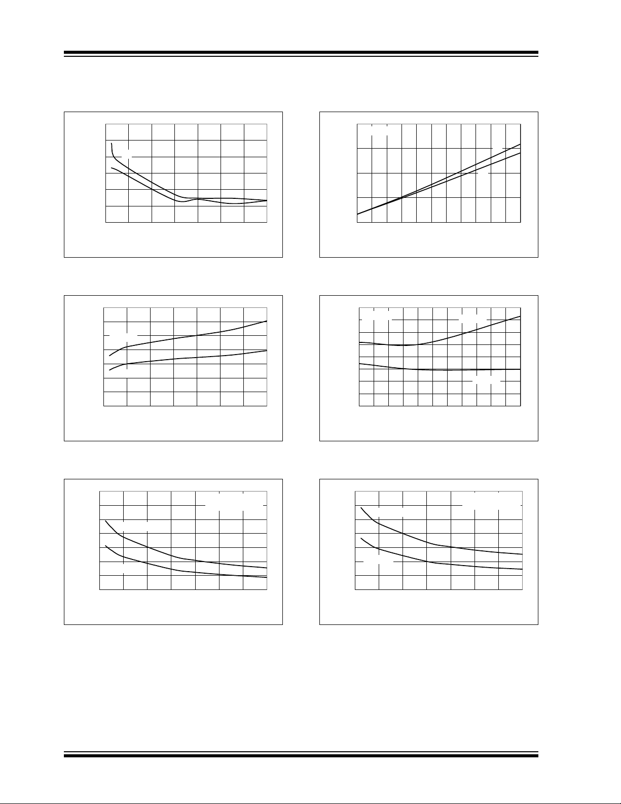
FIGURE 2-19: Input Threshold vs. Temperature.
FIGURE 2-20: Input Threshold vs. Supply Voltage.
FIGURE 2-22: Enable Hysteresis vs. Temperature.
FIGURE 2-23: Crossover Energy vs. Supply Voltage.
FIGURE 2-21: Enable Threshold vs. Temperature.
DS22062A-page 10 © 2007 Microchip Technology Inc.

MCP14E3/MCP14E4/MCP14E5
3.0 PIN DESCRIPTIONS
The descriptions of the pins are listed in Table 3-1.
TABLE 3-1: PIN FUNCTION TABLE
8-Pin
PDIP, SOIC
1 1 ENB_A Output A Enable
2 2 IN A Input A
3 3 GND Ground
4 4 IN B Input B
5 5 OUT B Output B
66V
7 7 OUT A Output A
8 8 ENB_B Output B Enable
— PAD NC Exposed Metal Pad
Note: Duplicate pins must be connected for proper operation.
8-Pin
6x5 DFN
Symbol Description
DD
Supply Input
3.1 Control Inputs A and B
The MOSFET driver inputs are a high-impedance TTL/
CMOS compatible input. The inputs also have hysteresis between the high and low input levels, allowing
them to be driven from slow rising and falling signals
and to provide noise immunity.
3.2 Outputs A and B
Outputs A and B are CMOS push-pull outputs that are
capable of sourcing and sinking 4.0A of peak current
= 18V). The low output impedance ensures the
(V
DD
gate of the MOSFET will stay in the intended state even
during large transients. These outputs also have a
reverse latch-up rating of 1.5A.
3.3 Supply Input (VDD)
VDD is the bias supply input for the MOSFET driver and
has a voltage range of 4.5V to 18V. This input must be
decoupled to ground with a local ceramic capacitor.
This bypass capacitor provides a localized low-impedance path for the peak currents that are to be provided
to the load.
3.4 Ground (GND)
3.5 Enable A (ENB_A)
The ENB_A pin is the enable control for Output A. This
enable pin is internally pulled up to VDD for active high
operation and can be left floating for standard
operation. When the ENB_A pin is pulled below the
enable pin Low Level Input Voltage (V
will be in the off state regardless of the input pin state.
EN_L
), Output A
3.6 Enable B (ENB_B)
The ENB_B pin is the enable control for Output B. This
enable pin is internally pulled up to VDD for active high
operation and can be left floating for standard
operation. When the ENB_B pin is pulled below the
enable pin Low-Level Input Voltage (V
will be in the off state regardless of the input pin state.
EN_L
), Output B
3.7 DFN Exposed Pad
The exposed metal pad of the DFN package is not
internally connected to any potential. Therefore, this
pad can be connected to a ground plane or other
copper plane on a printed circuit board to aid in heat
removal from the package.
Ground is the device return pin. The ground pin(s)
should have a low impedance connection to the bias
supply source return. High peak currents will flow out
the ground pin(s) when the capacitive load is being
discharged.
© 2007 Microchip Technology Inc. DS22062A-page 11

MCP14E3/MCP14E4/MCP14E5
0.1 µF
+5V
10%
90%
10%
90%
10%
90%
18V
1µF
0V
0V
MCP14E3
CL = 2200 pF
Input
Input
Output
t
D1
t
F
t
D2
Output
t
R
VDD = 18V
Ceramic
Input
(1/2 MCP14E5)
90%
Input
t
D1
t
F
t
D2
Output
t
R
10%
10%
10%
+5V
18V
0V
0V
90%
90%
0.1 µF
1µF
MCP14E4
CL = 2200 pF
Input Output
V
DD
= 18V
Ceramic
Input
(1/2 MCP14E5)
4.0 APPLICATION INFORMATION
4.1 General Information
MOSFET drivers are high-speed, high current devices
which are intended to source/sink high peak currents to
charge/discharge the gate capacitance of external
MOSFETs or IGBTs. In high frequency switching power
supplies, the PWM controller may not have the drive
capability to directly drive the power MOSFET. A MOSFET driver like the MCP14E3/MCP14E4/MCP14E5
family can be used to provide additional source/sink
current capability.
An additional degree of control has been added to the
MCP14E3/MCP14E4/MCP14E5 family. There are
separate enable functions for each driver that allow for
the immediate termination of the output pulse
regardless of the state of the input signal.
4.2 MOSFET Driver Timing
The ability of a MOSFET driver to transition from a fully
off state to a fully on state are characterized by the
drivers rise time (t
delays (tD1 and tD2). The MCP14E3/MCP14E4/
MCP14E5 family of drivers can typically charge and
discharge a 2200 pF load capacitance in 15 ns along
with a typical matched propagation delay of 50 ns.
Figure 4-1 and Figure 4-2 show the test circuit and
timing waveform used to verify the MCP14E3/
MCP14E4/MCP14E5 timing.
), fall time (tF), and propagation
R
FIGURE 4-2: Non-Inverting Driver Timing Waveform.
4.3 Enable Function
FIGURE 4-1: Inverting Driver Timing Waveform.
DS22062A-page 12 © 2007 Microchip Technology Inc.
The ENB_A and ENB_B enable pins allow for independent control of OUT A and OUT B respectively. They
are active high and are internally pulled up to V
DD
so
that the default state is to enable the driver. These pins
can be left floating for normal operation.
When an enable pin voltage is above the enable pin
high threshold voltage, V
(2.4V typical), that driver
EN_H
output is enabled and allowed to react to changes in
the INPUT pin voltage state. Likewise, when the enable
pin voltage falls below the enable pin low threshold
voltage, V
(2.0V typical), that driver output is dis-
EN_L
abled and does not respond the changes in the INPUT
pin voltage state. When the driver is disabled, the output goes to a low state. Refer to Table 4-1 for enable
pin logic. The threshold voltages of the enable function
are compatible with logic levels. Hysteresis is provided
to help increase the noise immunity of the enable
function, avoiding false triggers of the enable signal
during driver switching. For robust designs, it is
recommended that the slew rate of the enable pin
signal be greater than 1 V/ns.
There are propagation delays associated with the
driver receiving an enable signal and the output
reacting. These propagation delays, t
and tD4, are
D3
graphically represented in Figure 4-3.

MCP14E3/MCP14E4/MCP14E5
5V
0V
ENB_x
V
DD
0V
OUT x
V
EN_H
V
EN_L
90%
10%
t
D3
t
D4
P
T
PLPQP
CC
++=
Where:
P
T
= Total power dissipation
P
L
= Load power dissipation
P
Q
= Quiescent power dissipation
P
CC
= Operating power dissipation
P
L
fC
T
× V
DD
2
×=
Where:
f = Switching frequency
C
T
= Total load capacitance
V
DD
= MOSFET driver supply voltage
TABLE 4-1: ENABLE PIN LOGIC
MCP14E3 MCP14E4 MCP14E5
ENB_A ENB_B IN A IN B OUT A OUT B OUT A OUT B OUT A OUT B
HHHHL L HHLH
HHHL L HHL L L
HHLHH L LHHH
HHL L HHL L H L
LLXXLLLLLL
Placing a ground plane beneath the MCP14E3/
MCP14E4/MCP14E5 will help as a radiated noise
shield as well as providing some heat sinking for power
dissipated within the device.
4.6 Power Dissipation
The total internal power dissipation in a MOSFET driver
is the summation of three separate power dissipation
elements.
EQUATION 4-1:
FIGURE 4-3: Enable Timing Waveform.
4.4 Decoupling Capacitors
Careful layout and decoupling capacitors are highly
recommended when using MOSFET drivers. Large
currents are required to charge and discharge
capacitive loads quickly. For example, 2.5A are needed
to charge a 2200 pF load with 18V in 16 ns.
To operate the MOSFET driver over a wide frequency
range with low supply impedance, a ceramic and low
ESR film capacitor are recommended to be placed in
parallel between the driver V
ESR film capacitor and a 0.1 µF ceramic capacitor
should be used. These capacitors should be placed
close to the driver to minimized circuit board parasitics
and provide a local source for the required current.
4.5 PCB Layout Considerations
Proper PCB layout is important in a high current, fast
switching circuit to provide proper device operation and
robustness of design. PCB trace loop area and
inductance should be minimized by the use of ground
planes or trace under MOSFET gate drive signals,
separate analog and power grounds, and local driver
decoupling.
© 2007 Microchip Technology Inc. DS22062A-page 13
4.6.1 CAPACITIVE LOAD DISSIPATION
The power dissipation caused by a capacitive load is a
direct function of frequency, total capacitive load, and
supply voltage. The power lost in the MOSFET driver
for a complete charging and discharging cycle of a
MOSFET is:
EQUATION 4-2:
and GND. A 1.0 µF low
DD

MCP14E3/MCP14E4/MCP14E5
P
Q
I
QH
DIQL1 D–()×+×()VDD×=
Where:
I
QH
= Quiescent current in the high
state
D = Duty cycle
I
QL
= Quiescent current in the low
state
V
DD
= MOSFET driver supply voltage
P
CC
CC f× VDD×=
Where:
CC = Cross-conduction constant
(A*sec)
f = Switching frequency
V
DD
= MOSFET driver supply voltage
4.6.2 QUIESCENT POWER DISSIPATION
The power dissipation associated with the quiescent
current draw of the MCP14E3/MCP14E4/MCP14E5
depends upon the state of the input and enable pins.
Refer to the DC Characteristic table for the quiescent
current draw for specific combinations of input and
enable pin states. The quiescent power dissipation is:
EQUATION 4-3:
4.6.3 OPERATING POWER DISSIPATION
The operating power dissipation occurs each time the
MOSFET driver output transitions because for a very
short period of time both MOSFETs in the output stage
are on simultaneously. This cross-conduction current
leads to a power dissipation describes as:
EQUATION 4-4:
DS22062A-page 14 © 2007 Microchip Technology Inc.

MCP14E3/MCP14E4/MCP14E5
Legend: XX...X Customer-specific information
Y Year code (last digit of calendar year)
YY Year code (last 2 digits of calendar year)
WW Week code (week of January 1 is week ‘01’)
NNN Alphanumeric traceability code
Pb-free JEDEC designator for Matte Tin (Sn)
* This package is Pb-free. The Pb-free JEDEC designator ( )
can be found on the outer packaging for this package.
Note: In the event the full Microchip part number cannot be marked on one line, it will
be carried over to the next line, thus limiting the number of available
characters for customer-specific information.
3
e
XXXXXXXX
XXXXXNNN
YYWW
8-Lead PDIP (300 mil)
Example:
MCP14E3
E/P^^256
0737
8-Lead SOIC (150 mil)
Example:
256
MCP14E3E
8-Lead DFN
Example:
XXXXXXX
XXXXXXX
XXYYWW
NNN
MCP14E3
E/MF^^
0737
256
SN^^0737
NNN
XXXXXXXX
XXXXYYWW
5.0 PACKAGING INFORMATION
5.1 Package Marking Information (Not to Scale)
3
e
3
e
3
e
3
e
© 2007 Microchip Technology Inc. DS22062A-page 15
MCP14E3/MCP14E4/MCP14E5
8-Lead Plastic Dual Flat, No Lead Package (MF) – 6x5 mm Body [DFN-S]
PUNCH SINGULATED
Notes:
1. Pin 1 visual index feature may vary, but must be located within the hatched area.
2. Package may have one or more exposed tie bars at ends.
3. Dimensioning and tolerancing per ASME Y14.5M.
BSC: Basic Dimension. Theoretically exact value shown without tolerances.
REF: Ref erence Dimension, usually without tolerance, for information purposes only.
Note: For the most current package drawings, please see the Microchip Packaging Specification located at
http://www.microchip.com/packaging
Units M ILLIMETERS
Dimension Limits MIN NOM MAX
Number of Pins N 8
Pitch e 1.27 BSC
Overall Height A – 0.85 1.00
Molded Package Thickness A2 – 0.65 0.80
Standoff A1 0.00 0.01 0.05
Base Thickness A3 0.20 REF
Overall Length D 4.92 BSC
Molded Package Length D1 4.67 BSC
Exposed Pad Length D2 3.85 4.00 4.15
Overall Width E 5.99 BSC
Molded Package Width E1 5.74 BSC
Exposed Pad Width E2 2.16 2.31 2.46
Contact Width b 0.35 0.40 0.47
Contact Length L 0.50 0.60 0.75
Contact-to-Exposed Pad K 0.20 – –
Model Draft Angle Top φ – – 12°
φ
NOTE 2
A3
A2
A1
A
NOTE 1
NOTE 1
EXPOSED
PAD
BOTTOM VIEW
1
2
D2
2
1
E2
K
L
N
e
b
E
E1
D
D1
N
TOP VIEW
Microchip Technology Drawing C04-113B
DS22062A-page 16 © 2007 Microchip Technology Inc.
MCP14E3/MCP14E4/MCP14E5
8-Lead Plastic Dual In-Line (P) – 300 mil Body [PDIP]
Notes:
1. Pin 1 visual index feature may vary, but must be located with the hatched area.
2. § Significant Characteristic.
3. Dimensions D and E1 do not include mold flash or protrusions. Mold flash or protrusions shall not exceed .010" per side.
4. Dimens ioning and tolerancing per ASME Y14.5M.
BSC: Basic Dimension. Theoretically exact value shown without tolerances.
Note: For the most current package drawings, please see the Microchip Packaging Specification located at
http://www.microchip.com/packaging
Units INCHES
Dimension Limits MIN NOM MAX
Number of Pins N 8
Pitch e .100 BSC
Top to Seating Plane A – – .210
Molded Package Thickness A2 .115 .130 .195
Base to Seating Plane A1 .015 – –
Shoulder to Shoulder Width E .290 .310 .325
Molded Package Width E1 .240 .250 .280
Overall Length D .348 .365 .400
Tip to Seating Plane L .115 .130 .150
Lead Thickness c .008 .010 .015
Upper Lead Width b1 .040 .060 .070
Lower Lead Width b .014 .018 .022
Overall Row Spacing § eB – – .430
N
E1
NOTE 1
D
12
3
A
A1
A2
L
b1
b
e
E
eB
c
Microchip Technology Drawing C04-018B
© 2007 Microchip Technology Inc. DS22062A-page 17
MCP14E3/MCP14E4/MCP14E5
8-Lead Plastic Small Outline (SN) – Narrow, 3.90 mm Body [SOIC]
Notes:
1. Pin 1 visual index feature may vary, but must be located within the hatched area.
2. § Significant Characteristic.
3. Dimens ions D and E1 do not include mold flash or protrusions. Mold flash or protrusions shall not exceed 0.15 mm per side.
4. Dimens ioning and tolerancing per ASME Y14.5M.
BSC: Basic Dimension. Theoretically exact value shown without tolerances.
REF: Reference Dimension, usually without tolerance, for information purposes only.
Note: For the most current package drawings, please see the Microchip Packaging Specification located at
http://www.microchip.com/packaging
Units MILLIMETERS
Dimension Limits MIN NOM MAX
Number of Pins N 8
Pitch e 1.27 BSC
Overall Height A – – 1.75
Molded Package Thickness A2 1.25 – –
Standoff
§ A1 0.10 – 0.25
Overall Width E 6.00 BSC
Molded Package Width E1 3.90 BSC
Overall Length D 4.90 BSC
Chamfer (optional) h 0.25 – 0.50
Foot Length L 0.40 – 1.27
Footprint L1 1.04 REF
Foot Angle φ 0° – 8°
Lead Thickness c 0.17 – 0.25
Lead Width b 0.31 – 0.51
Mold Draft Angle Top α 5° – 15°
Mold Draft Angle Bottom β 5° – 15°
D
N
e
E
E1
NOTE 1
12 3
b
A
A1
A2
L
L1
c
h
h
φ
β
α
Microchip Technology Drawing C04-057B
DS22062A-page 18 © 2007 Microchip Technology Inc.

MCP14E3/MCP14E4/MCP14E5
/HDG3ODVWLF6PDOO2XWOLQH61±1DUURZPP%RG\>62,&@
1RWH )RUWKHPRVWFXUUHQWSDFNDJHGUDZLQJVSOHDVHVHHWKH0LFURFKLS3DFNDJLQJ6SHFLILFDWLRQORFDWHGDW
KWWSZZZPLFURFKLSFRPSDFNDJLQJ
© 2007 Microchip Technology Inc. DS22062A-page 19

MCP14E3/MCP14E4/MCP14E5
NOTES:
DS22062A-page 20 © 2007 Microchip Technology Inc.

MCP14E3/MCP14E4/MCP14E5
APPENDIX A: REVISION HISTORY
Revision A (September 2007)
• Original Release of this Document.
© 2007 Microchip Technology Inc. DS22062A-page 21

MCP14E3/MCP14E4/MCP14E5
NOTES:
DS22062A-page 22 © 2007 Microchip Technology Inc.

MCP14E3/MCP14E4/MCP14E5
Device: MCP14E3: 4.0A Dual MOSFET Driver, Inverting
MCP14E3T: 4.0A Dual MOSFET Driver, Inverting
Tape and Reel
MCP14E4: 4.0A Dual MOSFET Driver, Non-Inverting
MCP14E4T: 4.0A Dual MOSFET Driver, Non-Inverting
Tape and Reel
MCP14E5: 4.0A Dual MOSFET Driver, Complementary
MCP14E5T: 4.0A Dual MOSFET Driver, Complementary
Tape and Reel
Temperature Range: E = -40°C to +125°C
Package: * MF = Dual, Flat, No-Lead (6x5 mm Body), 8-lead
P = Plastic DIP, (300 mil body), 8-lead
SN = Plastic SOIC (150 mil Body), 8-Lead
* All package offerings are Pb Free (Lead Free)
Examples:
a) MCP14E3-E/MF: 4.0A Dual Inverting
MOSFET Driver,
8LD DFN package.
b) MCP14E3-E/P: 4.0A Dual Inverting
MOSFET Driver,
8LD PDIP package.
c) MCP14E3-E/SN: 4.0A Dual Inverting
MOSFET Driver,
8LD SOIC package.
a) MCP14E4-E/MF: 4.0A Dual Inverting
MOSFET Driver,
8LD DFN package.
b) MCP14E4-E/P: 4.0A Dual Inverting
MOSFET Driver,
8LD PDIP package.
c) MCP14E4T-E/SN: Tape and Reel,
4.0A Dual Inverting
MOSFET Driver,
8LD SOIC package.
a) MCP14E5T-E/MF: Tape and Reel,
4.0A Dual Inverting
MOSFET Driver,
8LD DFN package.
b) MCP14E5-E/P: 4.0A Dual Inverting
MOSFET Driver,
8LD PDIP package.
c) MCP14E5-E/SN: 4.0A Dual Inverting
MOSFET Driver,
8LD SOIC package.
PART NO. X XX
PackageTemperature
Range
Device
PRODUCT IDENTIFICATION SYSTEM
To order or obtain information, e.g., on pricing or delivery, refer to the factory or the listed sales office.
© 2007 Microchip Technology Inc. DS22062A-page 23

MCP14E3/MCP14E4/MCP14E5
NOTES:
DS22062A-page 24 © 2007 Microchip Technology Inc.

Note the following details of the code protection feature on Microchip devices:
• Microchip products meet the specification contained in their particular Microchip Data Sheet.
• Microchip believes that its family of products is one of the most secure families of its kind on the market today, when used in the
intended manner and under normal conditions.
• There are dishonest and possibly illegal methods used to breach the code protection feature. All of these methods, to our
knowledge, require using the Microchip products in a manner outside the operating specifications contained in Microchip’s Data
Sheets. Most likely, the person doing so is engaged in theft of intellectual property.
• Microchip is willing to work with the customer who is concerned about the integrity of their code.
• Neither Microchip nor any other semiconductor manufacturer can guarantee the security of their code. Code protection does not
mean that we are guaranteeing the product as “unbreakable.”
Code protection is constantly evolving. We at Microchip are committed to continuously improving the code protection features of our
products. Attempts to break Microchip’s code protection feature may be a violation of the Digital Millennium Copyright Act. If such acts
allow unauthorized access to your software or other copyrighted work, you may have a right to sue for relief under that Act.
Information contained in this publication regarding device
applications and the like is provided only for your convenience
and may be superseded by updates. It is your responsibility to
ensure that your application meets with your specifications.
MICROCHIP MAKES NO REPRESENTATIONS OR
WARRANTIES OF ANY KIND WHETHER EXPRESS OR
IMPLIED, WRITTEN OR ORAL, STATUTORY OR
OTHERWISE, RELATED TO THE INFORMATION,
INCLUDING BUT NOT LIMITED TO ITS CONDITION,
QUALITY, PERFORMANCE, MERCHANTABILITY OR
FITNESS FOR PURPOSE. Microchip disclaims all liability
arising from this information and its use. Use of Microchip
devices in life support and/or safety applications is entirely at
the buyer’s risk, and the buyer agrees to defend, indemnify and
hold harmless Microchip from any and all damages, claims,
suits, or expenses resulting from such use. No licenses are
conveyed, implicitly or otherwise, under any Microchip
intellectual property rights.
Trademarks
The Microchip name and logo, the Microchip logo, Accuron,
dsPIC, K
EELOQ, KEELOQ logo, microID, MPLAB, PIC,
PICmicro, PICSTART, PRO MATE, rfPIC and SmartShunt are
registered trademarks of Microchip Technology Incorporated
in the U.S.A. and other countries.
AmpLab, FilterLab, Linear Active Thermistor, Migratable
Memory, MXDEV, MXLAB, SEEVAL, SmartSensor and The
Embedded Control Solutions Company are registered
trademarks of Microchip Technology Incorporated in the
U.S.A.
Analog-for-the-Digital Age, Application Maestro, CodeGuard,
dsPICDEM, dsPICDEM.net, dsPICworks, dsSPEAK, ECAN,
ECONOMONITOR, FanSense, FlexROM, fuzzyLAB,
In-Circuit Serial Programming, ICSP, ICEPIC, Mindi, MiWi,
MPASM, MPLAB Certified logo, MPLIB, MPLINK, PICkit,
PICDEM, PICDEM.net, PICLAB, PICtail, PowerCal,
PowerInfo, PowerMate, PowerTool, REAL ICE, rfLAB, Select
Mode, Smart Serial, SmartTel, Total Endurance, UNI/O,
WiperLock and ZENA are trademarks of Microchip
Technology Incorporated in the U.S.A. and other countries.
SQTP is a service mark of Microchip Technology Incorporated
in the U.S.A.
All other trademarks mentioned herein are property of their
respective companies.
© 2007, Microchip Technology Incorporated, Printed in the
U.S.A., All Rights Reserved.
Printed on recycled paper.
Microchip received ISO/TS-16949:2002 certification for its worldwide
headquarters, design and wafer fabrication facilities in Chandler and
Tempe, Arizona; Gresham, Oregon and design centers in California
and India. The Company’s quality system processes and procedures
are for its PIC
devices, Serial EEPROMs, microperipherals, nonvolatile memory and
analog products. In addition, Microchip’s quality system for the design
and manufacture of development systems is ISO 9001:2000 certified.
®
MCUs and dsPIC® DSCs, KEELOQ
®
code hopping
© 2007 Microchip Technology Inc. DS22062A-page 25

WORLDWIDE SALES AND SERVICE
AMERICAS
Corporate Office
2355 West Chandler Blvd.
Chandler, AZ 85224-6199
Tel: 480-792-7200
Fax: 480-792-7277
Technical Support:
http://support.microchip.com
Web Address:
www.microchip.com
Atlanta
Duluth, GA
Tel: 678-957-9614
Fax: 678-957-1455
Boston
Westborough, MA
Tel: 774-760-0087
Fax: 774-760-0088
Chicago
Itasca, IL
Tel: 630-285-0071
Fax: 630-285-0075
Dallas
Addison, TX
Tel: 972-818-7423
Fax: 972-818-2924
Detroit
Farmington Hills, MI
Tel: 248-538-2250
Fax: 248-538-2260
Kokomo
Kokomo, IN
Tel: 765-864-8360
Fax: 765-864-8387
Los Angeles
Mission Viejo, CA
Tel: 949-462-9523
Fax: 949-462-9608
Santa Clara
Santa Clara, CA
Tel: 408-961-6444
Fax: 408-961-6445
Toronto
Mississauga, Ontario,
Canada
Tel: 905-673-0699
Fax: 905-673-6509
ASIA/PACIFIC
Asia Pacific Office
Suites 3707-14, 37th Floor
Tower 6, The Gateway
Harbour City, Kowloon
Hong Kong
Tel: 852-2401-1200
Fax: 852-2401-3431
Australia - Sydney
Tel: 61-2-9868-6733
Fax: 61-2-9868-6755
China - Beijing
Tel: 86-10-8528-2100
Fax: 86-10-8528-2104
China - Chengdu
Tel: 86-28-8665-5511
Fax: 86-28-8665-7889
China - Fuzhou
Tel: 86-591-8750-3506
Fax: 86-591-8750-3521
China - Hong Kong SAR
Tel: 852-2401-1200
Fax: 852-2401-3431
China - Nanjing
Tel: 86-25-8473-2460
Fax: 86-25-8473-2470
China - Qingdao
Tel: 86-532-8502-7355
Fax: 86-532-8502-7205
China - Shanghai
Tel: 86-21-5407-5533
Fax: 86-21-5407-5066
China - Shenyang
Tel: 86-24-2334-2829
Fax: 86-24-2334-2393
China - Shenzhen
Tel: 86-755-8203-2660
Fax: 86-755-8203-1760
China - Shunde
Tel: 86-757-2839-5507
Fax: 86-757-2839-5571
China - Wuhan
Tel: 86-27-5980-5300
Fax: 86-27-5980-5118
China - Xian
Tel: 86-29-8833-7252
Fax: 86-29-8833-7256
ASIA/PACIFIC
India - Bangalore
Tel: 91-80-4182-8400
Fax: 91-80-4182-8422
India - New Delhi
Tel: 91-11-4160-8631
Fax: 91-11-4160-8632
India - Pune
Tel: 91-20-2566-1512
Fax: 91-20-2566-1513
Japan - Yokohama
Tel: 81-45-471- 6166
Fax: 81-45-471-6122
Korea - Daegu
Tel: 82-53-744-4301
Fax: 82-53-744-4302
Korea - Seoul
Tel: 82-2-554-7200
Fax: 82-2-558-5932 or
82-2-558-5934
Malaysia - Kuala Lumpur
Tel: 60-3-6201-9857
Fax: 60-3-6201-9859
Malaysia - Penang
Tel: 60-4-646-8870
Fax: 60-4-646-5086
Philippines - Manila
Tel: 63-2-634-9065
Fax: 63-2-634-9069
Singapore
Tel: 65-6334-8870
Fax: 65-6334-8850
Taiwan - Hsin Chu
Tel: 886-3-572-9526
Fax: 886-3-572-6459
Taiwan - Kaohsiung
Tel: 886-7-536-4818
Fax: 886-7-536-4803
Taiwan - Taipei
Tel: 886-2-2500-6610
Fax: 886-2-2508-0102
Thailand - Bangkok
Tel: 66-2-694-1351
Fax: 66-2-694-1350
EUROPE
Austria - Wels
Tel: 43-7242-2244-39
Fax: 43-7242-2244-393
Denmark - Copenhagen
Tel: 45-4450-2828
Fax: 45-4485-2829
France - Paris
Tel: 33-1-69-53-63-20
Fax: 33-1-69-30-90-79
Germany - Munich
Tel: 49-89-627-144-0
Fax: 49-89-627-144-44
Italy - Milan
Tel: 39-0331-742611
Fax: 39-0331-466781
Netherlands - Drunen
Tel: 31-416-690399
Fax: 31-416-690340
Spain - Madrid
Tel: 34-91-708-08-90
Fax: 34-91-708-08-91
UK - Wokingham
Tel: 44-118-921-5869
Fax: 44-118-921-5820
09/10/07
DS22062A-page 26 © 2007 Microchip Technology Inc.
 Loading...