

Page 1
MCP131X/2X
1
2
3
5
4
MCP1317
1
2
3
5
4
MCP1318/18M/21
1
2
3
5
4
MCP1319/19M/22
1
2
3
5
4
MCP1316/16M/20
SOT-23-5
RST
RST
V
SS
MR
WDI
V
DD
V
DD
RST
V
SS
MR
WDI
V
SS
RST
WDI
V
DD
RST
V
SS
RST
MR
V
DD
V
DD
Comparator
+
–
Output
Driver
RST
Reference
V
SS
RST
Noise Filter
Watchdog
MR
WDI
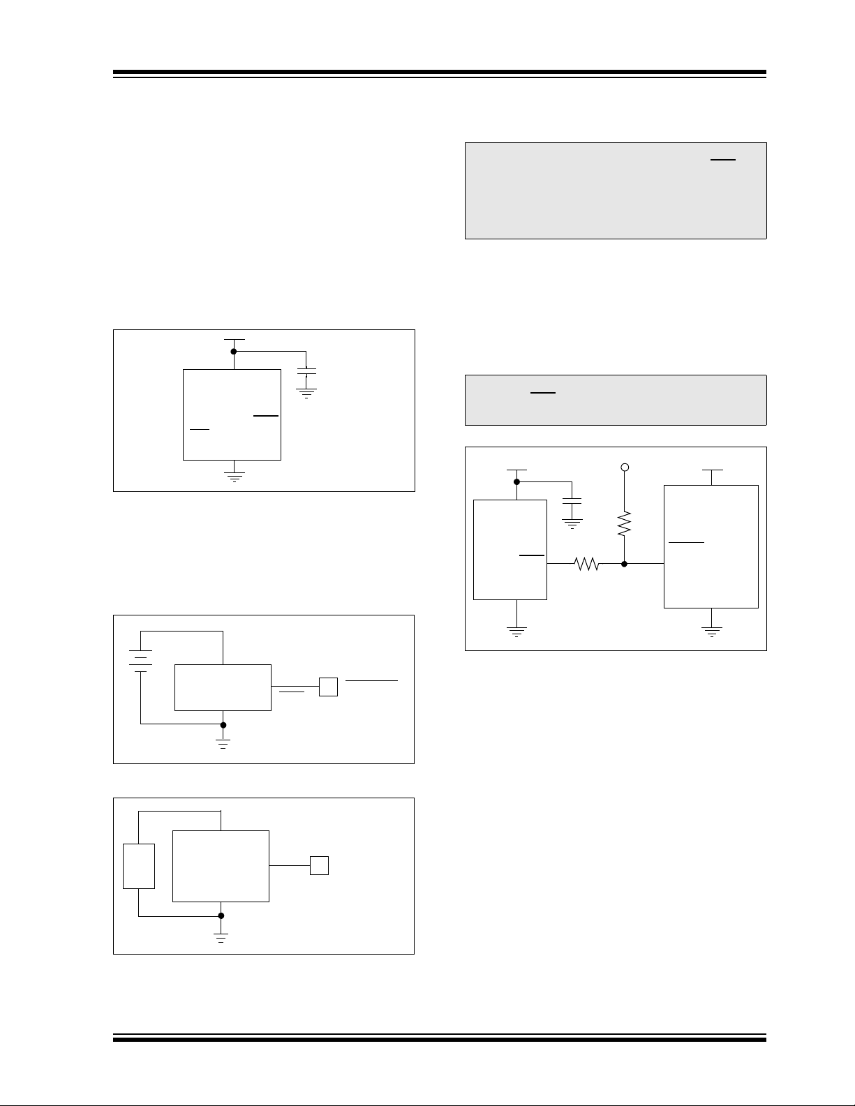
Note: Features available depend on the device
Voltage
Voltage Supervisor
Features
• Low supply current: 1 µA (typical),10 µA (max.)
• Precision monitoring trip point options:
- 2.9V and 4.6V (Standard Offerings)
- 2.0V to 4.7V in 100 mV increments,
(Contact the local Microchip Sales Office)
• Resets microcontroller in a power-l oss event
• Reset Delay Time Out Option:
- 1.4 ms, 30 ms, 200 ms, or 1.6s (typical)
• Watchdog Timer Input Time Out Options:
- 6.3 ms, 102 ms, 1.6s, or 25.6s (typical)
• Manual Reset (MR
• Single and Complementary Reset output(s)
• Reset Output Options:
- Push-Pull (active-high or active-low)
- Open-Drain (internal or external Pull-up)
• Temperature Range:
- -40°C to +85°C for trip points 2.0 to 2.4V and,
- -40°C to + 125°C for trip points > 2.5V
• Voltage Range: 1.0V to 5.5V
• Lead Free Packaging
) input (active-low)
Description
The MCP131X/2X are voltage supervisor devices
designed to keep a microcontroller in Reset until the
system voltage has reached and stabilized at the
proper level for reliable system operation. The table
below shows the available features for these devices.
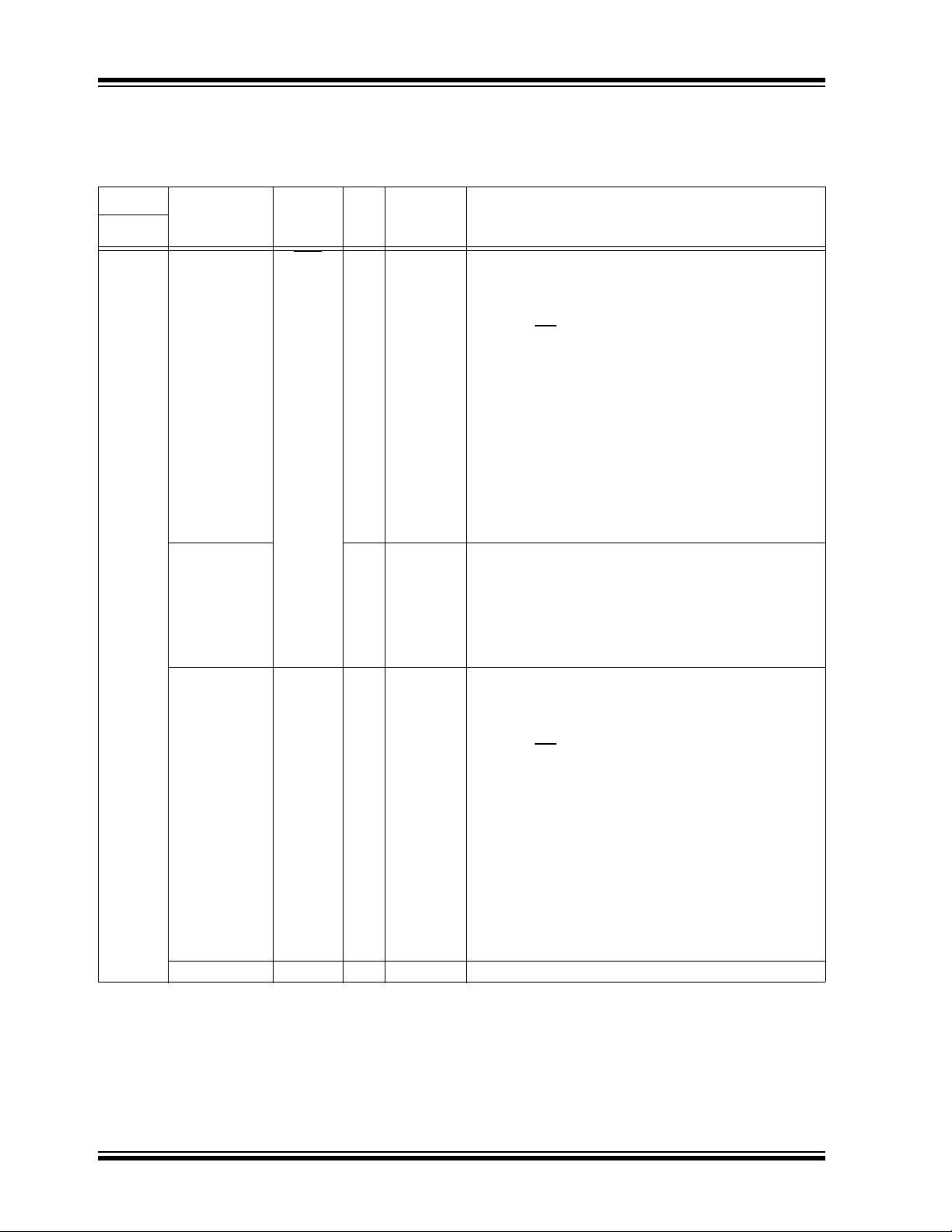
Package Types
Block Diagram
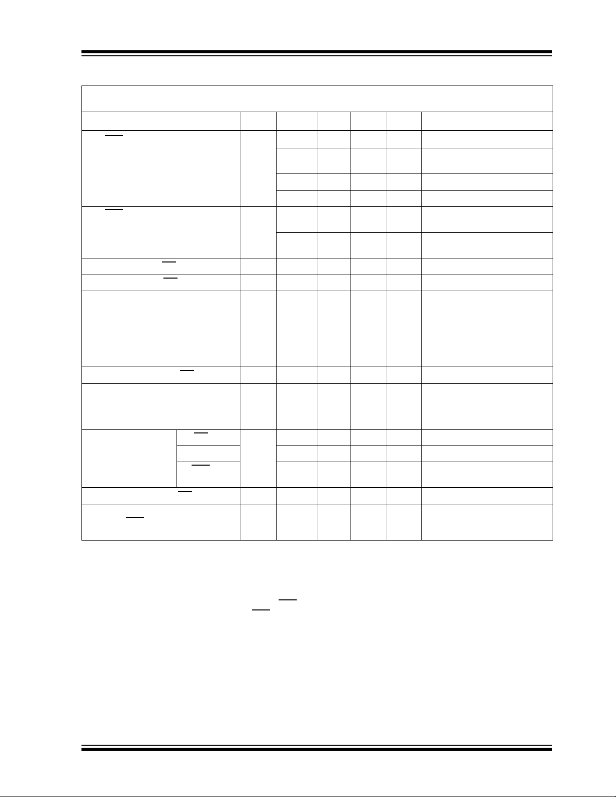
Device Features
Device
MCP1316 Push-Pull — Low — — — Yes Yes
MCP1316M Open-Drain Internal Low — — — Yes Yes
MCP1317 Push-Pull — High — — — Yes Yes
MCP1318 Push-Pull — Low Push-Pull — High Yes No
MCP1318M Open-Drain Internal Low Push-Pull — High Yes No
MCP1319 Push-Pull — Low Push-Pull — High No Yes
MCP1319M Open-Drain Internal Low Push-Pull — High No Yes
MCP1320 Open-Drain External Low — — — Yes Yes
MCP1321 Open-Drain External Low Push-Pull — High Yes No
MCP1322 Open-Drain External Low Push-Pull — High No Yes
© 2007 Microchip Technology Inc. DS21985B-page 1
Type
Reset Output A Reset Output B
Pull-up
Resistor
Active
Level
Type
Pull-up
Resistor
Active
Level
WDI Input MR Input
Page 2
MCP131X/2X
1.0 ELECTRICAL CHARACTERISTICS
Absolute Maximum Ratings†
Supply Voltage (VDD to VSS). . . . . . . . . . . . . . . . . . . . . . 7.0V
Input current (V
Output current (RST
Voltage on all inputs and outputs, except Open-Drain RST
(with no internal pull-up resistor), w.r.t. V
. . . . . . . . . . . . . . . . . . . . . . . . . . . . . . .-0.6V to (V
Voltage on Open-Drain RST
(with no internal pull-up resistor) w.r.t. V
Storage temperature. . . . . . . . . . . . . . . . . . .-65°C to +150°C
Ambient temp. with power applied . . . . . . . .-40°C to +125°C
Maximum Junction temp. with power applied . . . . . . . .150°C
Power Dissipation (T
5-Pin SOT-23A.......................................................240 mW
ESD protection on all pins..................................................≥ 4kV
) . . . . . . . . . . . . . . . . . . . . . . . . . . . .10 mA
DD
) . . . . . . . . . . . . . . . . . . . . . . . . . .10 mA
≤ 70°C):
A
SS
. . -0.6V to 13.5V
SS
+ 1.0V)
DD
† Notice: Stresses above those listed under “Maximum Ratings” may cause permanent damage to the device. This is a
stress rating only and functional operation of the device at
those or any other conditions above those indicated in the
operational listings of this specification is not implied. Exposure to maximum rating conditions for extended periods may
affect device reliability.
DC CHARACTERISTICS
Electrical Specifications: Unless otherwise indicated, all limits are specified for VDD = 1V to 5.5V, RPU = 100 kΩ
(only MCP1320, MCP1321, and MCP1322), T
Parameters Sym Min Typ Max Units Conditions
= -40°C to +125°C.
A
Operating Voltage Range V
Specified VDD Value to V
Low V
OUT
Operating Current: I
DD
DD
DD
1.0 — 5.5 V
1.0 — — V I
= 10 µA, V
RST
RST
— 5 10 µA Watchdog Timer Active
— 1 2 µA Watchdog Timer Inactive
—12µAVDD < V
TRIP
— 5 10 µA Reset Delay Timer Active
Note 1: Trip point is ±1.5% from typical value.
2: Trip point is ±2.5% from typical value.
3: Hyster ysis is minimum = 1%, maximum = 6% at +25°C.
4: This specification allows this device to be used in PIC
®
microcontroller applications that require the In-Circuit Serial Programming™ (ICSP™) feature (see device-specific programming specifications for voltage
requirements). The total time that the RST pin can be above the maximum device operational voltage
(5.5V) is 100s. Current into the RST
pin should be limited to 2 mA. It is recommended that the device operational temperature be maintained between 0°C to +70°C (+25°C preferred). For additional information,
refer to Figure 2-35.
5: This parameter is established by characterization and is not 100% tested.
6: Custom ordered voltage trip point; min imum ord er volume requ irement . Informati on avai labl e upo n reque st.
< 0.3V
DS21985B-page 2 © 2007 Microchip Technology Inc.
Page 3
MCP131X/2X
DC CHARACTERISTICS (CONTINUED)
Electrical Specifications: Unless otherwise indicated, all limits are specified for VDD = 1V to 5.5V, RPU = 100 kΩ
(only MCP1320, MCP1321, and MCP1322), T
Parameters Sym Min Typ Max Units Conditions
= -40°C to +125°C.
A
VDD Trip Point MCP13XX-20 V
(Note 6) 1.950 2.00 2.050 V TA = -40°C to +85°C (Note 2)
MCP13XX-21 2.069 2.10 2.132 V TA = +25°C (Note 1)
(Note 6) 2.048 2.10 2.153 V TA = -40°C to +85°C (Note 2)
MCP13XX-22 2.167 2.20 2.233 V TA = +25°C (Note 1)
(Note 6) 2.145 2.20 2.255 V TA = -40°C to +85°C (Note 2)
MCP13XX-23 2.266 2.30 2.335 V TA = +25°C (Note 1)
(Note 6) 2.243 2.30 2.358 V TA = -40°C to +85°C (Note 2)
MCP13XX-24 2.364 2.40 2.436 V TA = +25°C (Note 1)
(Note 6) 2.340 2.40 2.460 V TA = -40°C to +85°C (Note 2)
MCP13XX-25 2.463 2.50 2.538 V TA = +25°C (Note 1)
(Note 6) 2.438 2.50 2.563 V TA = -40°C to +125°C (Note 2)
MCP13XX-26 2.561 2.60 2.639 V TA = +25°C (Note 1)
(Note 6) 2.535 2.60 2.665 V TA = -40°C to +125°C (Note 2)
MCP13XX-27 2.660 2.70 2.741 V TA = +25°C (Note 1)
(Note 6) 2.633 2.70 2.768 V TA = -40°C to +125°C (Note 2)
MCP13XX-28 2.758 2.80 2.842 V TA = +25°C (Note 1)
(Note 6) 2.730 2.80 2.870 V TA = -40°C to +125°C (Note 2)
MCP13XX-29 2.857 2.90 2.944 V T
MCP13XX-30 2.955 3.00 3.045 V TA = +25°C (Note 1)
(Note 6) 2.925 3.00 3.075 V TA = -40°C to +125°C (Note 2)
MCP13XX-31 3.054 3.10 3.147 V TA = +25°C (Note 1)
(Note 6) 3.023 3.10 3.178 V TA = -40°C to +125°C (Note 2)
MCP13XX-32 3.152 3.20 3.248 V TA = +25°C (Note 1)
(Note 6) 3.120 3.20 3.280 V TA = -40°C to +125°C (Note 2)
MCP13XX-33 3.251 3.30 3.350 V TA = +25°C (Note 1)
(Note 6) 3.218 3.30 3.383 V TA = -40°C to +125°C (Note 2)
Note 1: Trip point is ±1.5% from typical value.
2: Trip point is ±2.5% from typical value.
3: Hyster ysis is minimum = 1%, maximum = 6% at +25°C.
4: This specification allows this device to be used in PIC
cuit Serial Programming™ (ICSP™) feature (see device-specific programming specifications for voltage
requirements). The total time that the RST
(5.5V) is 100s. Current into the RST
ational temperature be maintained between 0°C to +70°C (+25°C preferred). For additional information,
refer to Figure 2-35.
5: This parameter is established by characterization and is not 100% tested.
6: Custom ordered voltage trip point; min imum ord er volume requ irement . Informati on avai labl e upo n reque st.
TRIP
1.970 2.00 2.030 V TA = +25°C (Note 1)
= +25°C (Note 1)
A
2.828 2.90 2.973 V TA = -40°C to +125°C (Note 2)
®
microcontroller applications that require the In-Cir-
pin can be above the maximum device operational voltage
pin should be limited to 2 mA. It is recommended that the device oper-
© 2007 Microchip Technology Inc. DS21985B-page 3
Page 4

MCP131X/2X
DC CHARACTERISTICS (CONTINUED)
Electrical Specifications: Unless otherwise indicated, all limits are specified for VDD = 1V to 5.5V, RPU = 100 kΩ
(only MCP1320, MCP1321, and MCP1322), T
Parameters Sym Min Typ Max Units Conditions
= -40°C to +125°C.
A
VDD Trip Point (Con’t) MCP13XX-34 V
TRIP
3.349 3.40 3.451 V TA = +25°C (Note 1)
(Note 6) 3.315 3.40 3.385 V TA = -40°C to +125°C (Note 2)
MCP13XX-35 3.448 3.50 3.553 V TA = +25°C (Note 1)
(Note 6) 3.413 3.50 3.588 V TA = -40°C to +125°C (Note 2)
MCP13XX-36 3.546 3.60 3.654 V TA = +25°C (Note 1)
(Note 6) 3.510 3.60 3.690 V TA = -40°C to +125°C (Note 2)
MCP13XX-37 3.645 3.70 3.756 V TA = +25°C (Note 1)
(Note 6) 3.608 3.70 3.793 V TA = -40°C to +125°C (Note 2)
MCP13XX-38 3.743 3.80 3.857 V TA = +25°C (Note 1)
(Note 6) 3.705 3.80 3.895 V TA = -40°C to +125°C (Note 2)
MCP13XX-39 3.842 3.90 3.959 V TA = +25°C (Note 1)
(Note 6) 3.803 3.90 3.998 V TA = -40°C to +125°C (Note 2)
MCP13XX-40 3.940 4.00 4.060 V TA = +25°C (Note 1)
(Note 6) 3.900 4.00 4.100 V TA = -40°C to +125°C (Note 2)
MCP13XX-41 4.039 4.10 4.162 V TA = +25°C (Note 1)
(Note 6) 3.998 4.10 4.203 V TA = -40°C to +125°C (Note 2)
MCP13XX-42 4.137 4.20 4.263 V TA = +25°C (Note 1)
(Note 6) 4.095 4.20 4.305 V TA = -40°C to +125°C (Note 2)
MCP13XX-43 4.236 4.30 4.365 V TA = +25°C (Note 1)
(Note 6) 4.193 4.30 4.408 V TA = -40°C to +125°C (Note 2)
MCP13XX-44 4.334 4.40 4.466 V TA = +25°C (Note 1)
(Note 6) 4.290 4.40 4.510 V TA = -40°C to +125°C (Note 2)
MCP13XX-45 4.433 4.50 4.568 V TA = +25°C (Note 1)
(Note 6) 4.388 4.50 4.613 V TA = -40°C to +125°C (Note 2)
MCP13XX-46 4.531 4.60 4.669 V T
4.485 4.60 4.715 V T
= +25°C (Note 1)
A
= -40°C to +125°C (Note 2)
A
MCP13XX-47 4.630 4.70 4.771 V TA = +25°C (Note 1)
(Note 6) 4.583 4.70 4.818 V TA = -40°C to +125°C (Note 2)
V
Trip Point Tempco
DD
T
TPCO
— ±40 — ppm/°C
Note 1: Trip point is ±1.5% from typical value.
2: Trip point is ±2.5% from typical value.
3: Hyster ysis is minimum = 1%, maximum = 6% at +25°C.
4: This specification allows this device to be used in PIC
®
microcontroller applications that require the In-Circuit Serial Programming™ (ICSP™) feature (see device-specific programming specifications for voltage
requirements). The total time that the RST
(5.5V) is 100s. Current into the RST
pin can be above the maximum device operational voltage
pin should be limited to 2 mA. It is recommended that the device operational temperature be maintained between 0°C to +70°C (+25°C preferred). For additional information,
refer to Figure 2-35.
5: This parameter is established by characterization and is not 100% tested.
6: Custom ordered voltage trip point; min imum ord er volume requ irement . Informati on avai labl e upo n reque st.
DS21985B-page 4 © 2007 Microchip Technology Inc.
Page 5

MCP131X/2X
DC CHARACTERISTICS (CONTINUED)
Electrical Specifications: Unless otherwise indicated, all limits are specified for VDD = 1V to 5.5V, RPU = 100 kΩ
(only MCP1320, MCP1321, and MCP1322), T
Parameters Sym Min Typ Max Units Conditions
= -40°C to +125°C.
A
Threshold Hysteresis MCP13XX-20 V
(Note 3) (Note 6) (Note 6) V TA = -40°C to +85°C
MCP13XX-21 0.021 — 0.126 V TA = +25°C (Note 3)
(Note 6) (Note 6) V TA = -40°C to +85°C
MCP13XX-22 0.022 — 0.132 V TA = +25°C (Note 3)
(Note 6) (Note 6) V TA = -40°C to +85°C
MCP13XX-23 0.023 — 0.138 V TA = +25°C (Note 3)
(Note 6) (Note 6) V TA = -40°C to +85°C
MCP13XX-24 0.024 — 0.144 V TA = +25°C (Note 3)
(Note 6) (Note 6) V TA = -40°C to +85°C
MCP13XX-25 0.025 — 0.150 V TA = +25°C (Note 3)
(Note 6) (Note 6) V TA = -40°C to +125°C
MCP13XX-26 0.026 — 0.156 V TA = +25°C (Note 3)
(Note 6) (Note 6) V TA = -40°C to +125°C
MCP13XX-27 0.027 — 0.162 V TA = +25°C (Note 3)
(Note 6) (Note 6) V TA = -40°C to +125°C
MCP13XX-28 0.028 — 0.168 V TA = +25°C (Note 3)
(Note 6) (Note 6) V TA = -40°C to +125°C
MCP13XX-29 0.029 — 0.174 V T
MCP13XX-30 0.030 — 0.180 V TA = +25°C (Note 3)
(Note 6) (Note 6) V TA = -40°C to +125°C
MCP13XX-31 0.031 — 0.186 V TA = +25°C (Note 3)
(Note 6) (Note 6) V TA = -40°C to +125°C
MCP13XX-32 0.032 — 0.192 V TA = +25°C (Note 3)
(Note 6) (Note 6) V TA = -40°C to +125°C
MCP13XX-33 0.033 — 0.198 V TA = +25°C (Note 3)
(Note 6) (Note 6) V TA = -40°C to +125°C
Note 1: Trip point is ±1.5% from typical value.
2: Trip point is ±2.5% from typical value.
3: Hyster ysis is minimum = 1%, maximum = 6% at +25°C.
4: This specification allows this device to be used in PIC
cuit Serial Programming™ (ICSP™) feature (see device-specific programming specifications for voltage
requirements). The total time that the RST
(5.5V) is 100s. Current into the RST
ational temperature be maintained between 0°C to +70°C (+25°C preferred). For additional information,
refer to Figure 2-35.
5: This parameter is established by characterization and is not 100% tested.
6: Custom ordered voltage trip point; min imum ord er volume requ irement . Informati on avai labl e upo n reque st.
HYS
0.020 — 0.120 V TA = +25°C (Note 3)
= +25°C (Note 3)
A
(Note 6) VTA = -40°C to +125°C
®
microcontroller applications that require the In-Cir-
pin can be above the maximum device operational voltage
pin should be limited to 2 mA. It is recommended that the device oper-
© 2007 Microchip Technology Inc. DS21985B-page 5
Page 6
MCP131X/2X
DC CHARACTERISTICS (CONTINUED)
Electrical Specifications: Unless otherwise indicated, all limits are specified for VDD = 1V to 5.5V, RPU = 100 kΩ
(only MCP1320, MCP1321, and MCP1322), T
Parameters Sym Min Typ Max Units Conditions
= -40°C to +125°C.
A
Threshold Hysteresis MCP13XX-34 V
(Continued) (Note 3) (Note 6) (Note 6) V TA = -40°C to +125°C
MCP13XX-35 0.035 — 0.210 V TA = +25°C (Note 3)
(Note 6) (Note 6) V TA = -40°C to +125°C
MCP13XX-36 0.036 — 0.216 V TA = +25°C (Note 3)
(Note 6) (Note 6) V TA = -40°C to +125°C
MCP13XX-37 0.037 — 0.222 V TA = +25°C (Note 3)
(Note 6) (Note 6) V TA = -40°C to +125°C
MCP13XX-38 0.038 — 0.228 V TA = +25°C (Note 3)
(Note 6) (Note 6) V TA = -40°C to +125°C
MCP13XX-39 0.039 — 0.234 V TA = +25°C (Note 1)
(Note 6) (Note 6) V TA = -40°C to +125°C
MCP13XX-40 0.040 — 0.240 V TA = +25°C (Note 3)
(Note 6) (Note 6) V TA = -40°C to +125°C
MCP13XX-41 0.041 — 0.246 V TA = +25°C (Note 3)
(Note 6) (Note 6) V TA = -40°C to +125°C
MCP13XX-42 0.042 — 0.252 V TA = +25°C (Note 3)
(Note 6) (Note 6) V TA = -40°C to +125°C
MCP13XX-43 0.043 — 0.258 V TA = +25°C (Note 3)
(Note 6) (Note 6) V TA = -40°C to +125°C
MCP13XX-44 0.044 — 0.264 V TA = +25°C (Note 3)
(Note 6) (Note 6) V TA = -40°C to +125°C
MCP13XX-45 0.045 — 0.270 V TA = +25°C (Note 3)
(Note 6) (Note 6) V TA = -40°C to +125°C
MCP13XX-46 0.046 — 0.276 V T
MCP13XX-47 0.047 — 0.282 V TA = +25°C (Note 3)
(Note 6) (Note 6) V TA = -40°C to +125°C
Note 1: Trip point is ±1.5% from typical value.
2: Trip point is ±2.5% from typical value.
3: Hyster ysis is minimum = 1%, maximum = 6% at +25°C.
4: This specification allows this device to be used in PIC
cuit Serial Programming™ (ICSP™) feature (see device-specific programming specifications for voltage
requirements). The total time that the RST
(5.5V) is 100s. Current into the RST
ational temperature be maintained between 0°C to +70°C (+25°C preferred). For additional information,
refer to Figure 2-35.
5: This parameter is established by characterization and is not 100% tested.
6: Custom ordered voltage trip point; min imum ord er volume requ irement . Informati on avai labl e upo n reque st.
HYS
0.034 — 0.204 V TA = +25°C (Note 3)
= +25°C (Note 3)
A
(Note 6) VT
®
microcontroller applications that require the In-Cir-
pin can be above the maximum device operational voltage
pin should be limited to 2 mA. It is recommended that the device oper-
= -40°C to +125°C
A
DS21985B-page 6 © 2007 Microchip Technology Inc.
Page 7
MCP131X/2X
DC CHARACTERISTICS (CONTINUED)
Electrical Specifications: Unless otherwise indicated, all limits are specified for VDD = 1V to 5.5V, RPU = 100 kΩ
(only MCP1320, MCP1321, and MCP1322), T
Parameters Sym Min Typ Max Units Conditions
= -40°C to +125°C.
A
RST/RST Low-Level Output Voltage V
RST/RST High-Level Output Voltage V
OL
OH
(Push-Pull Outputs only) V
Input Low Voltage (MR
and WDI pins) VIL VSS —0.3VDD V
——0.3VI
——0.3VI
——0.3VI
——0.3VI
VDD –
—— VI
0.7
–
DD
0.7
—— VI
OL
OL
1.5V < V
OL
OL
OH
OH
= 50 µA, 1.0V ≤ V
= 100 µA,
≤ 2.5V
DD
= 2 mA, 2.5V < V
= 4 mA, VDD > 4.5V
= 2.5 mA, VDD ≥ 2.5V
= 500 µA, VDD ≥ 1.5V
Input High Voltage (MR and WDI pins) VIH 0.7VDD —VDD V
Open-Drain High Voltage on Output
(Note 4)
V
— — 13.5
ODH
(4)
V Open-Drain Output pin only,
= 3.0V, Time voltage >
V
DD
5.5V applied ≤ 100 s,
current into pin limited to 2 mA,
+25°C operation recommended
(Note 4, Note 5)
Input Leakage Current (MR
Open-Drain Output Leakage Current
(MCP1316M, MCP1318M,
and WDI) IIL ——±1µAVSS ≤ V
I
OD
—0.0031.0 µA
PIN
≤ V
DD
MCP1319M, MCP1320, MCP1321,
and MCP1322 only)
Pull-up Resistance MR
pin RPU —52—kΩ VDD = 5.5V
WDI pin — 52 — kΩ V
DD
= 5.5V
RST pin — 4.7 — kΩ VDD = 5.5V,
MCP131XM devices only
Input Pin Capacitance (MR
Output Pin Capacitive Loading
(RST and RST
)
and WDI) CI — 100 — pF
— — 50 pF This is the tester loading to
C
O
meet the AC timing specifica-
tions.
Note 1: Trip point is ±1.5% from typical value.
2: Trip point is ±2.5% from typical value.
3: Hyster ysis is minimum = 1%, maximum = 6% at +25°C.
4: This specification allows this device to be used in PIC
®
microcontroller applications that require the In-Circuit Serial Programming™ (ICSP™) feature (see device-specific programming specifications for voltage
requirements). The total time that the RST
(5.5V) is 100s. Current into the RST
pin can be above the maximum device operational voltage
pin should be limited to 2 mA. It is recommended that the device operational temperature be maintained between 0°C to +70°C (+25°C preferred). For additional information,
refer to Figure 2-35.
5: This parameter is established by characterization and is not 100% tested.
6: Custom ordered voltage trip point; min imum ord er volume requ irement . Informati on avai labl e upo n reque st.
DD
DD
≤ 1.5V
≤ 4.5V
© 2007 Microchip Technology Inc. DS21985B-page 7
Page 8
MCP131X/2X
V
TRIPMAX
V
TRIPMIN
V
TRIP
1V
V
DD
V
TRIPAC
+ V
HYS
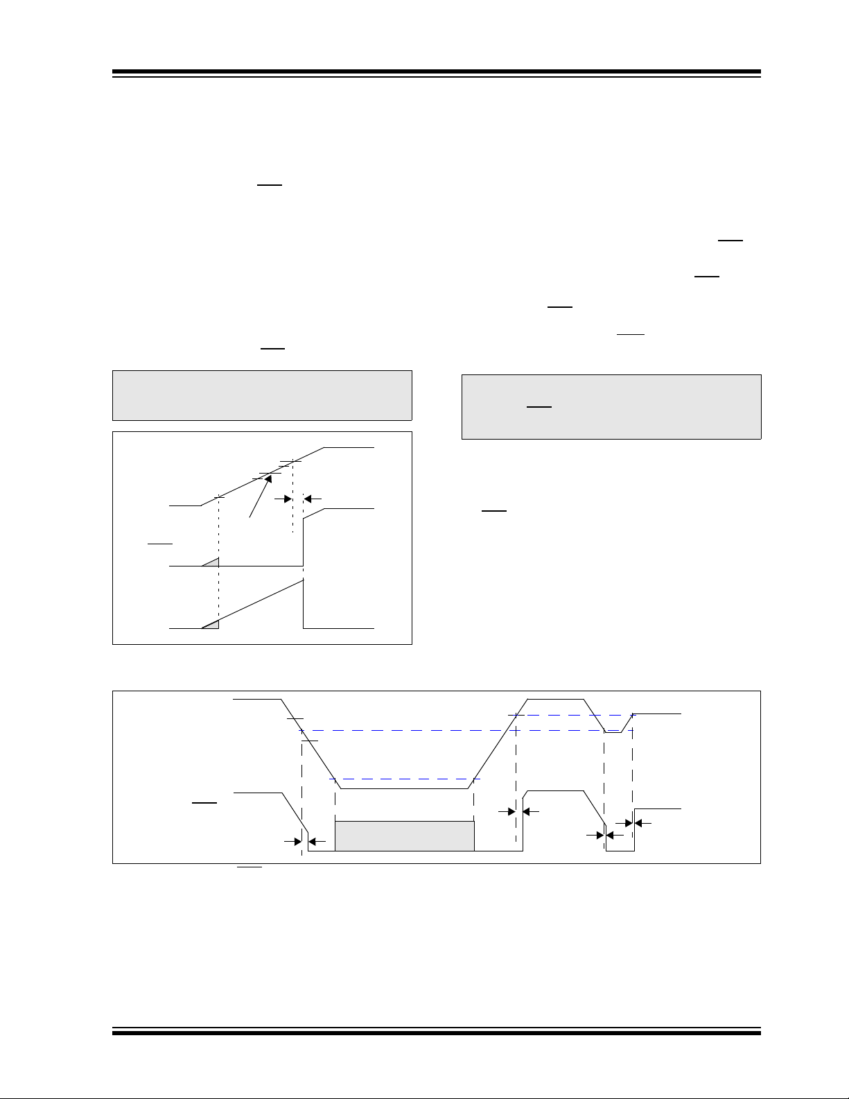
t
RST
RST
RST
tRR
t
RST
t
RPD
VDD < 1V is outside the device operating specification. The RST (or RST) output state is
unknown while V
DD
< 1V.
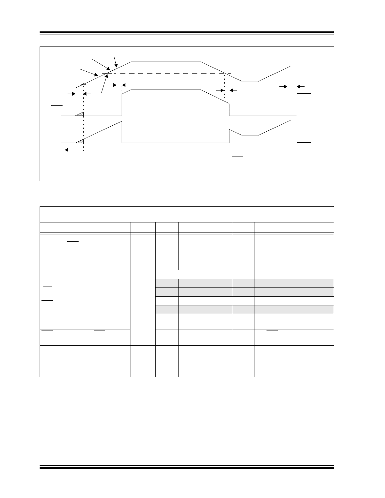
FIGURE 1-1: Device Voltage and Reset Pin Waveforms.
TABLE 1-1: DEVICE VOLTAGE AND RESET PIN TIMINGS
Electrical Specifications: Unless otherwise indicated, all limits are specified for VDD = 1V to 5.5V, RPU = 100 kΩ
(only MCP1320, MCP1321, and MCP1322), T
Parameters Sym Min Typ Max Units Conditions
Falling V
Trip Point Detected
DD
t
RPD
to RST or RST Active
VDD Rise Rate t
Reset active time
(MR
Rising Edge, POR/BOR
t
RST
Inactive, or WDT time out) to RST/
Inactive
RST
RST Rise Time after RST
Active
t
(Push-Pull Outputs only)
RST
Rise Time after RST Inactive
(Push-Pull Outputs only)
RST Fall Time after RST
RST
Fall Time after RST Active — 5 — µs For RST 90% to 10% of VDD,
Note 1: These parameters are for design guidance only and are not 100% tested.
Inactive t
2: Custom ordered Reset active time; minimum order volume requirement.
3: Designed to be independent of V
0.1 V/s (@ +25°C).
= -40°C to +125°C.
A
—650 — µsVDD ramped from
V
TRIPMAX
V
TRIPMIN
+ 250 mV down to
– 200 mV,
VDD falling @ 5 mV/µs,
CL = 50 pF (Note 1)
RR
Note 3
1.0 1.4 2.0 ms Note 2
20 30 40 ms Note 2
140 200 280 ms Standard Time Out
1120 1600 2240 ms Note 2
RT
— 5 — µs For RST 10% to 90% of VDD,
= 50 pF (Note 1)
C
L
—5 —µsFor RST 10% to 90% of VDD,
= 50 pF (Note 1)
C
L
FT
— 5 — µs For RST 90% to 10% of VDD,
CL = 50 pF (Note 1)
= 50 pF (Note 1)
C
L
rise rate. Device characterization was done with a rise rate as slow as
DD
DS21985B-page 8 © 2007 Microchip Technology Inc.
Page 9
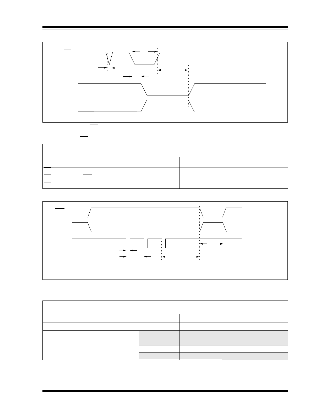
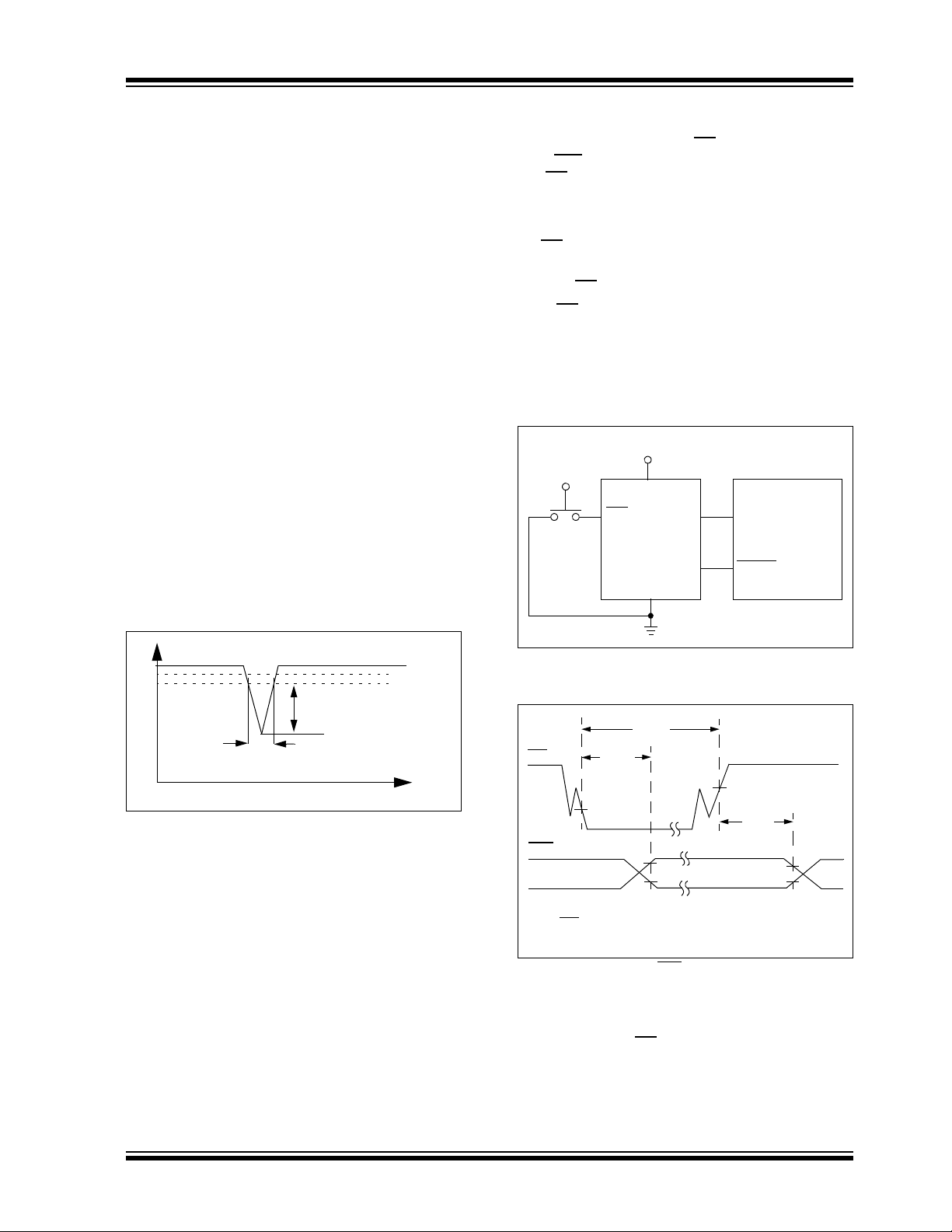
MR
RST
t
RST
t
MR
RST
t
MRD
t
NF
RST
RST
WDI (Note 1)
t
WP
t
WD
t
WD
t
RST
Note 1: The WDI pin was a weak pull-up resistor which is disabled after the 1st falling edge on the WDI pin.
FIGURE 1-2: MR and Reset Pin Waveforms.
MCP131X/2X
TABLE 1-2: MR
AND RESET PIN TIMINGS
Electrical Specifications: Unless otherwise indicated, all limits are specified for VDD = 1V to 5.5V, RPU = 100 kΩ
(only MCP1320, MCP1321, and MCP1322), TA = -40°C to +125°C.
Parameters Sym Min Typ Max Units Conditions
MR
Pulse Width t
MR Active to RST/RST Active t
MR
Input Noise filter t
MR
MRD
NF
1— —µs
—235 — nsVDD = 5.0V
—150 — nsVDD = 5.0V
Note 1: These parameters are for design guidance only and are not 100% tested.
FIGURE 1-3: WDI and Reset Pin Waveforms.
TABLE 1-3: WDI AND RESET PIN TIMINGS
Electrical Specifications: Unless otherwise indicated, all limits are specified for V
(only MCP1320, MCP1321, and MCP1322), T
= -40°C to +125°C.
A
Parameters Sym Min Typ Max Units Conditions
WDI Pulse Width t
Watchdog Time Out Period t
Note 1: Custom ordered WatchDog Timer time out; minimum order volume requirement.
© 2007 Microchip Technology Inc. DS21985B-page 9
50 — — ns
WP
4.3 6.3 9.3 ms Note 1
WD
71 102 153 ms Note 1
1.12 1.6 2.4 sec Standard Time Out
17.9 25.6 38.4 sec Note 1
= 1V to 5.5V, RPU = 100 kΩ
DD
Page 10
MCP131X/2X
TEMPERATURE CHARACTERISTICS
Electrical Specifications: Unless otherwise noted, all limits are specified for VDD = 1V to 5.5V, RPU = 100 kΩ
(only MCP1316), T
Parameters Sym Min Typ Max Units Conditions
Temperature Ranges
Specified Temperature Range T
Specified Temperature Range T
Maximum Junction Temperature T
Storage Temperature Range T
Package Thermal Resistances
Thermal Resistance, 5L-SOT23 θ
= -40°C to +125°C.
A
JA
A
A
J
A
-40 — +85 °C MCP13XX-25 (or below)
-40 — +125 °C Except MCP13XX-25 (or below)
——+150°C
-65 — +150 °C
— 255.9 — °C/W
DS21985B-page 10 © 2007 Microchip Technology Inc.
Page 11
MCP131X/2X
0
0.2
0.4
0.6
0.8
1
1.2
-100 -50 0 50 100 150
Temperature (°C)
I
DD
(µA)
1.0V 1.5V 2.0V
3.0V 4.3V 4.5V
4.8V 5.0V 5.5V
0
0.2
0.4
0.6
0.8
1
1.2
1.4
-100 -50 0 50 100 150
Temperature (°C)
I
DD
(µA)
1.0V 1.5V 2.5V
2.7V 3.2V 4.0V
4.5V 5.0V 5.5V
0
0.2
0.4
0.6
0.8
1
1.2
1.4
1.6
1.8
-100 -50 0 50 100 150
Temperature (°C)
I
DD
(µA)
1.0V 1.5V 1.8V
2.2V 2.5V 4.0V
4.5V 5.0V 5.5V
0
1
2
3
4
5
6
-100 -50 0 50 100 150
Temperature (°C)
Idd (µA)
4.8V 5.0V 5.5V
0
1
2
3
4
5
6
-100 -50 0 50 100 150
Temperature (°C)
I
DD
(µA)
3.2V 4.0V 4.5V 5.0V 5.5V
0
1
2
3
4
5
6
7
-100 -50 0 50 100 150
Temperature (°C)
I
DD
(µA)
2.2V 2.5V 4.0V 4.5V 5.0V 5.5V
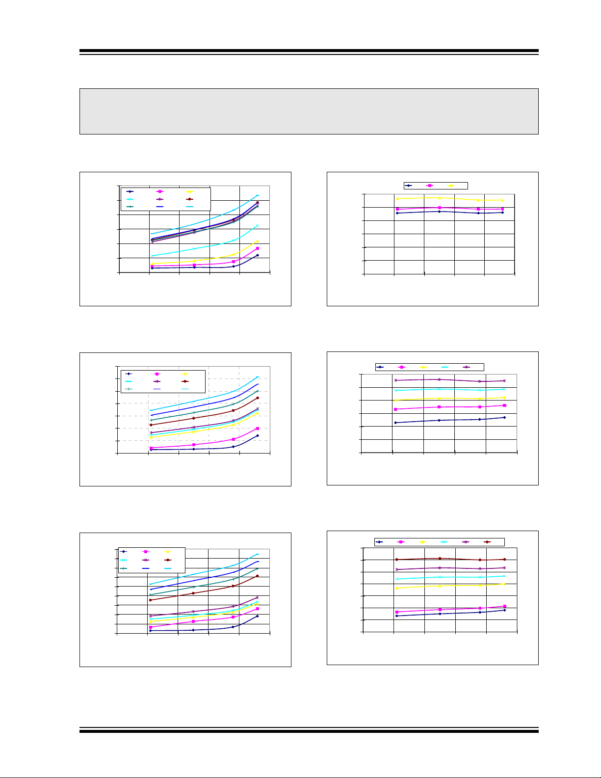
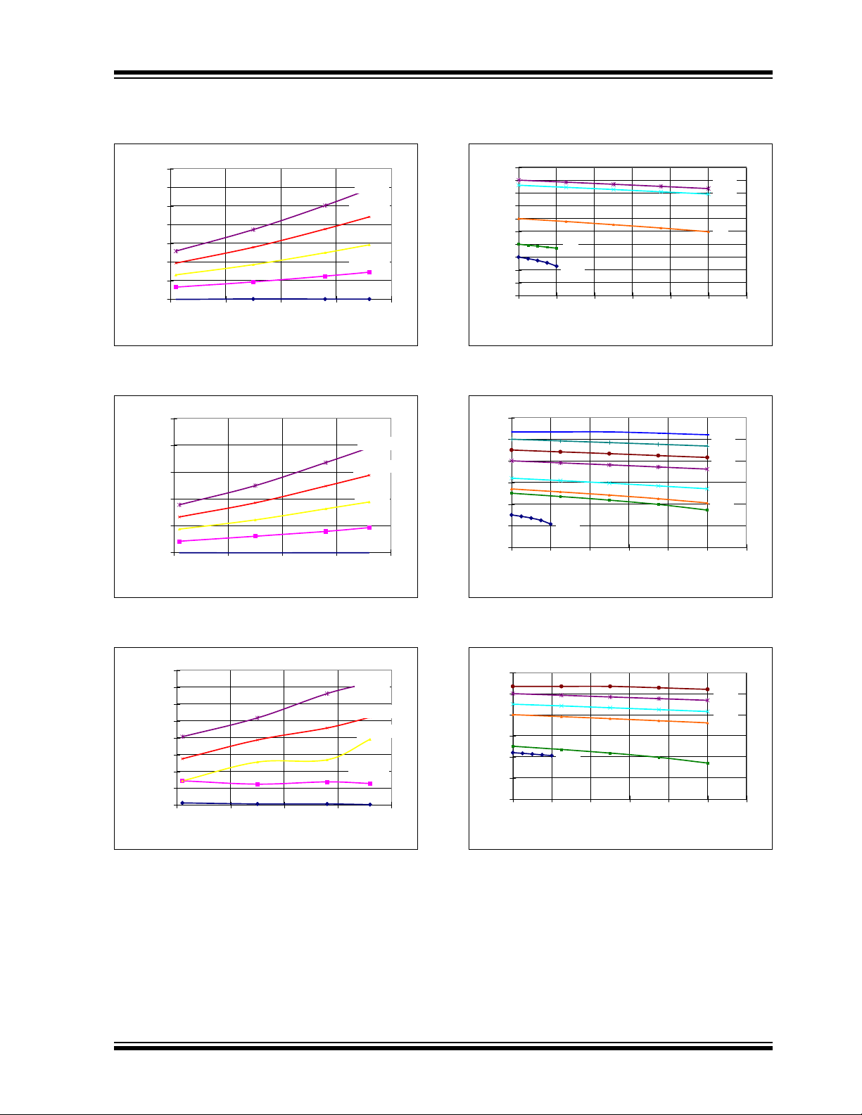
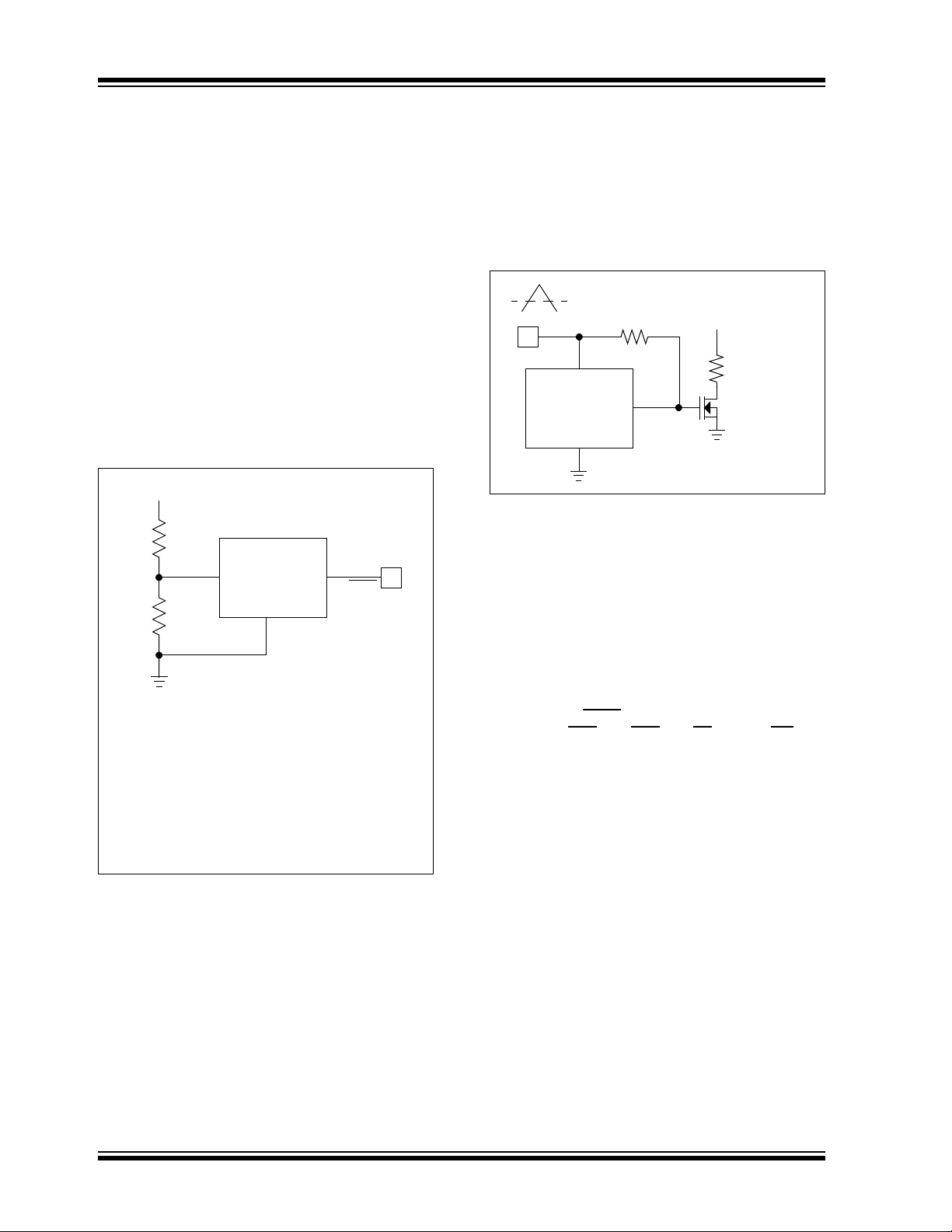
2.0 TYPICAL PERFORMANCE CURVES
Note: The graphs and tables provided following this note are a statistical summary based on a limited number of
samples and are provided for informational purposes only. The performance characteristics listed herein
are not tested or guaranteed. In some graphs or tables, the data presented may be outside the specified
operating range (e.g., outside specified power supply range) and therefore outside the warranted range.
Note: Unless otherwise indicated, all limits are specified for VDD = 1V to 5.5V, RPU = 100 kΩ (only MCP1316;
see Figure 4-1), TA = -40°C to +125°C.
FIGURE 2-1: IDD vs. Temperature (Reset Power-up Timer Inactive and Watchdog Timer Inactive) (MCP1318M-4.6).
FIGURE 2-2: I
vs. Temperature (Reset
DD
Power-up Timer Inactive and Watchdog Timer
Inactive) (MCP1319-2.9).
FIGURE 2-4: I
vs. Temperature (Reset
DD
Power-up Timer Active) (MCP1318M-4.6).
FIGURE 2-5: I
vs. Temperature (Reset
DD
Power-up Timer Active) (MCP1319-2.9).
FIGURE 2-3: I
Power-up Timer Inactive and Watchdog Timer
Inactive) (MCP1316-2.0).
© 2007 Microchip Technology Inc. DS21985B-page 11
vs. Temperature (Reset
DD
FIGURE 2-6: I
vs. Temperature (Reset
DD
Power-up Timer Active) (MCP1316-2.0).
Page 12
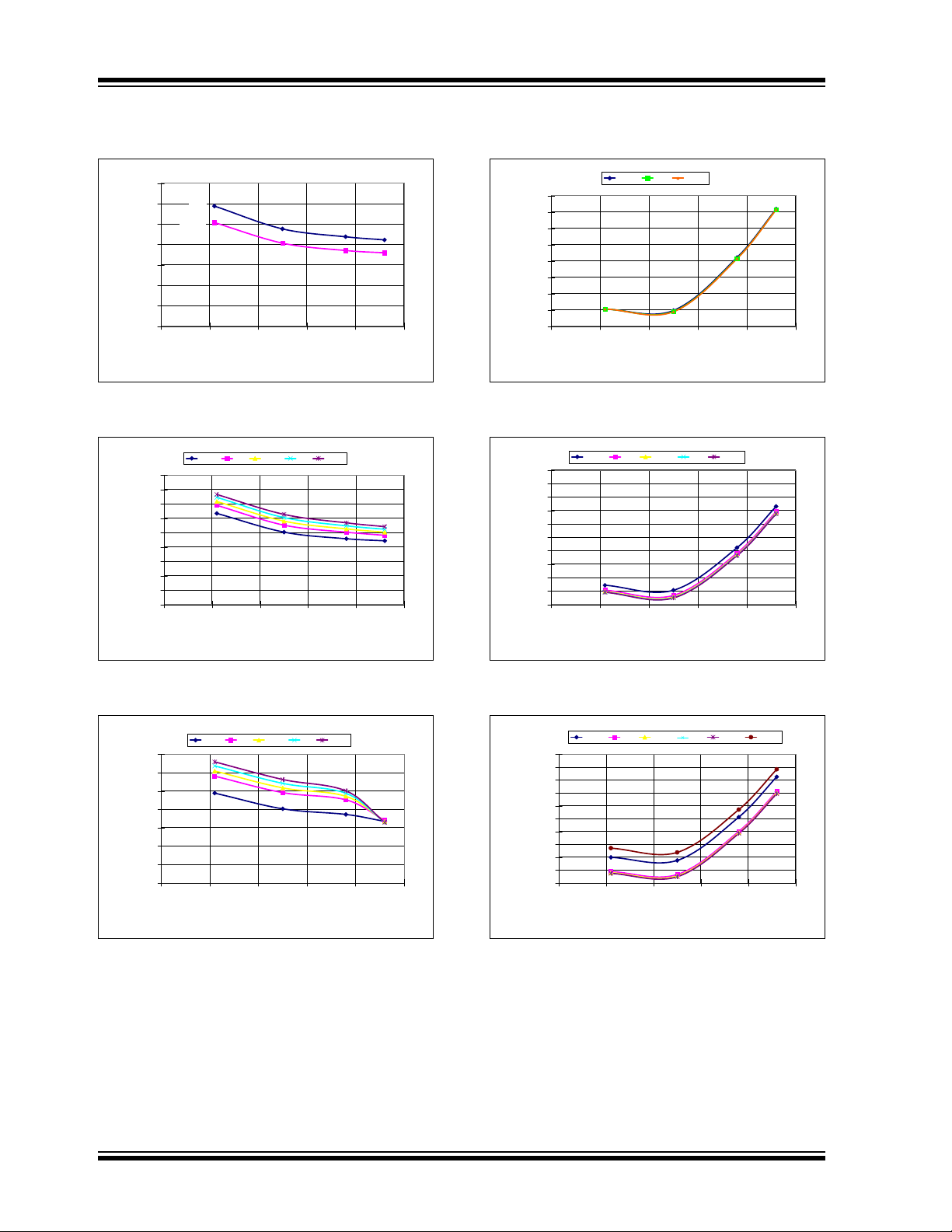
MCP131X/2X
0
1
2
3
4
5
6
7
-100 -50 0 50 100 150
Temperature (°C)
I
DD
(µA)
4.8V 5.0V 5.5V
MCP1319 does not
have a Watchdog Timer
0
1
2
3
4
5
6
7
-100 -50 0 50 100 150
Temperature (°C)
I
DD
(µA)
2.2V 2.5V 4.0V 4.5V 5.0V 5.5V
Note: Unless otherwise indicated, all limits are specified for VDD = 1V to 5.5V, RPU = 100 kΩ (only MCP1316;
see Figure 4-1), TA = -40°C to +125°C.
FIGURE 2-7: IDD vs. Temperature (Watchdog Timer Active) (MCP1318M-4.6).
FIGURE 2-8: I
vs. Temperature
DD
(Watchdog Timer Active) (MCP1319-2.9).
FIGURE 2-9: I
DD
(Watchdog Timer Active) (MCP1316-2.0).
DS21985B-page 12 © 2007 Microchip Technology Inc.
vs. Temperature
Page 13
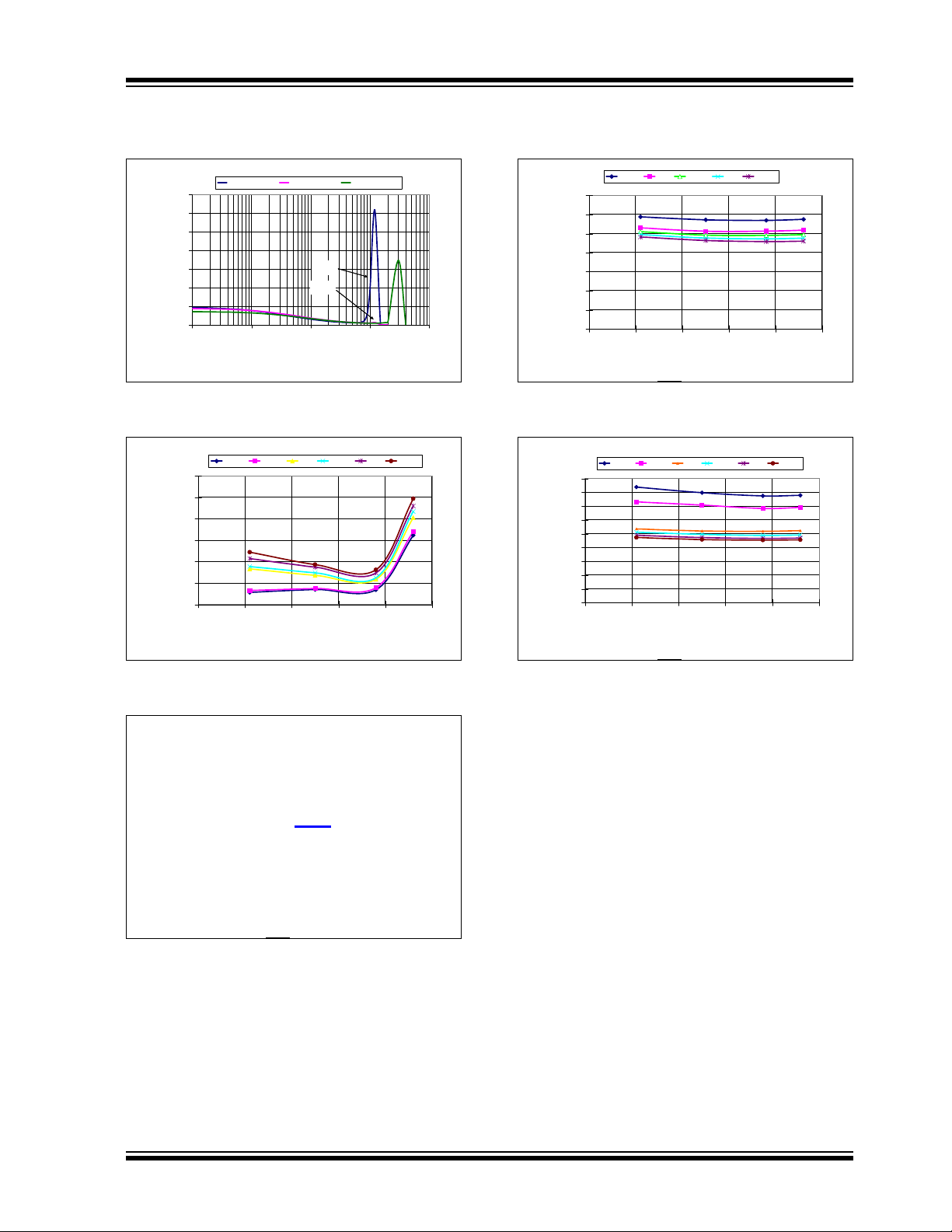
MCP131X/2X
0
0.2
0.4
0.6
0.8
1
1.2
0.0 1.0 2.0 3.0 4.0 5.0 6.0
V
DD
(V)
I
DD
(µA)
-45°C
25°C
90°C
130°C
0
0.2
0.4
0.6
0.8
1
1.2
1.4
0.0 1.0 2.0 3.0 4.0 5.0 6.0
V
DD
(V)
I
DD
(µA)
-45°C
25°C
90°C
130°C
0
0.2
0.4
0.6
0.8
1
1.2
1.4
1.6
1.8
0.0 1.0 2.0 3.0 4.0 5.0 6.0
V
DD
(V)
I
DD
(µA)
-45°C
25°C
90°C
130°C
0
1
2
3
4
5
6
4.6 4.8 5.0 5.2 5.4 5.6
V
DD
(V)
I
DD
(µA)
-45°C 25°C 90°C 130°C
0
1
2
3
4
5
6
0.0 1.0 2.0 3.0 4.0 5.0 6.0
V
DD
(V)
I
DD
(µA)
-45°C 25°C 90°C 130°C
0
1
2
3
4
5
6
7
2.0 3.0 4.0 5.0 6.0
V
DD
(V)
I
DD
(µA)
-45°C 25°C 90°C 130°C
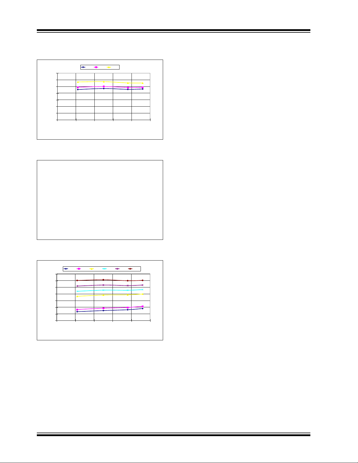
Note: Unless otherwise indicated, all limits are specified for VDD = 1V to 5.5V, RPU = 100 kΩ (only MCP1316;
see Figure 4-1), TA = -40°C to +125°C.
FIGURE 2-10: IDD vs. VDD (Reset Power- up Timer Inactive and Watchdog Timer Inactive) (MCP1318M-4.6).
FIGURE 2-11: I
vs. VDD (Reset Power-
DD
up Timer Inactive and Watchdog Timer Inactive)
(MCP1319-2.9).
FIGURE 2-13: I
vs. VDD (Reset Power-
DD
up Timer Active or Watchdog Timer Active)
(MCP1318M-4.6).
FIGURE 2-14: I
vs. VDD (Reset Power-
DD
up Timer Active or Watchdog Timer Active)
(MCP1319-2.9).
FIGURE 2-12: I
up Timer Inactive and Watchdog Timer Inactive)
(MCP1316-2.0).
© 2007 Microchip Technology Inc. DS21985B-page 13
vs. VDD (Reset Power-
DD
FIGURE 2-15: I
vs. VDD (Reset Power-
DD
up Timer Active or Watchdog Timer Active)
(MCP1316-2.0).
Page 14
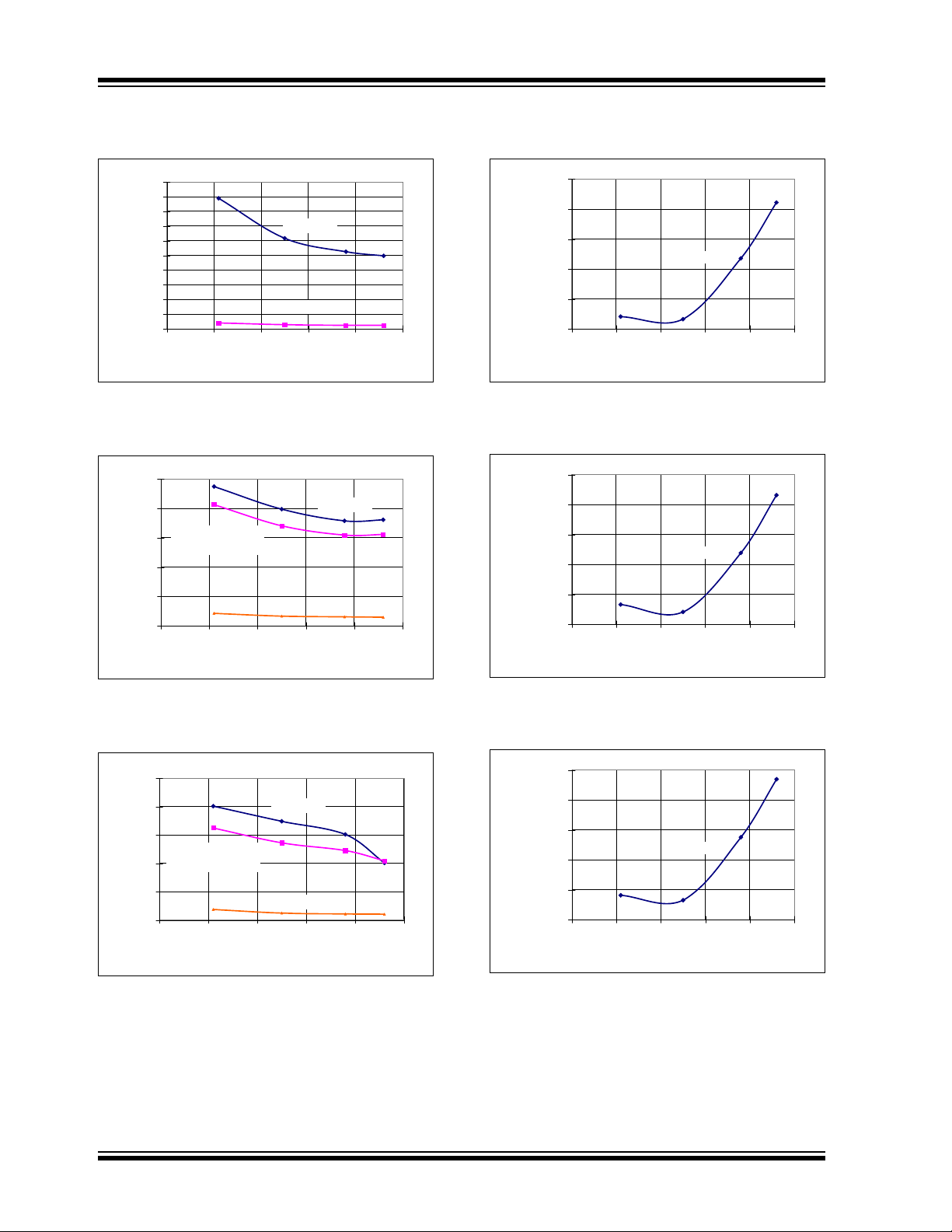
MCP131X/2X
4.550
4.600
4.650
4.700
4.750
4.800
-50 0 50 100 150
Temperature (°C)
V
TRIP
(V)
3.0
3.1
3.2
3.3
3.4
3.5
3.6
3.7
3.8
3.9
4.0
V
TRIP
Hyst (%)
V
HYST
V
TRIP
Down
V
TRIP
Up
2.880
2.900
2.920
2.940
2.960
2.980
3.000
3.020
-50 0 50 100 150
Temperature (°C)
V
TRIP
(V)
3.0
3.1
3.1
3.2
3.2
3.3
3.3
3.4
3.4
3.5
V
TRIP
Hyst (%)
V
HYST
V
TRIP
Down
V
TRIP
Up
1.990
2.000
2.010
2.020
2.030
2.040
2.050
-50 0 50 100 150
Temperature (°C)
V
TRIP
(V)
0.0
0.5
1.0
1.5
2.0
2.5
3.0
V
TRIP
Hyst (%)
V
HYST
V
TRIP
Down
V
TRIP
Up
0
0.02
0.04
0.06
0.08
0.1
0.12
0.14
0.16
0.00 2.00 4.00 6.00 8.00 10.00
I
OL
(mA)
V
OL
(V)
1V 2V 3V 4.3V 4.5V 4.8V 5V 5.5V
0
0.02
0.04
0.06
0.08
0.1
0.12
0.14
0.16
0.00 2.00 4.00 6.00 8.00 10.00
I
OL
(mA)
V
OL
(V)
1V 2.5V 2.7V 3.2V 4V 4.5V 5V 5.5V
0
0.002
0.004
0.006
0.008
0.01
0.012
0.014
0.016
0.018
0.02
0.00 0.05 0.10 0.15 0.20 0.25
I
OL
(mA)
V
OL
(V)
1V
1.8V
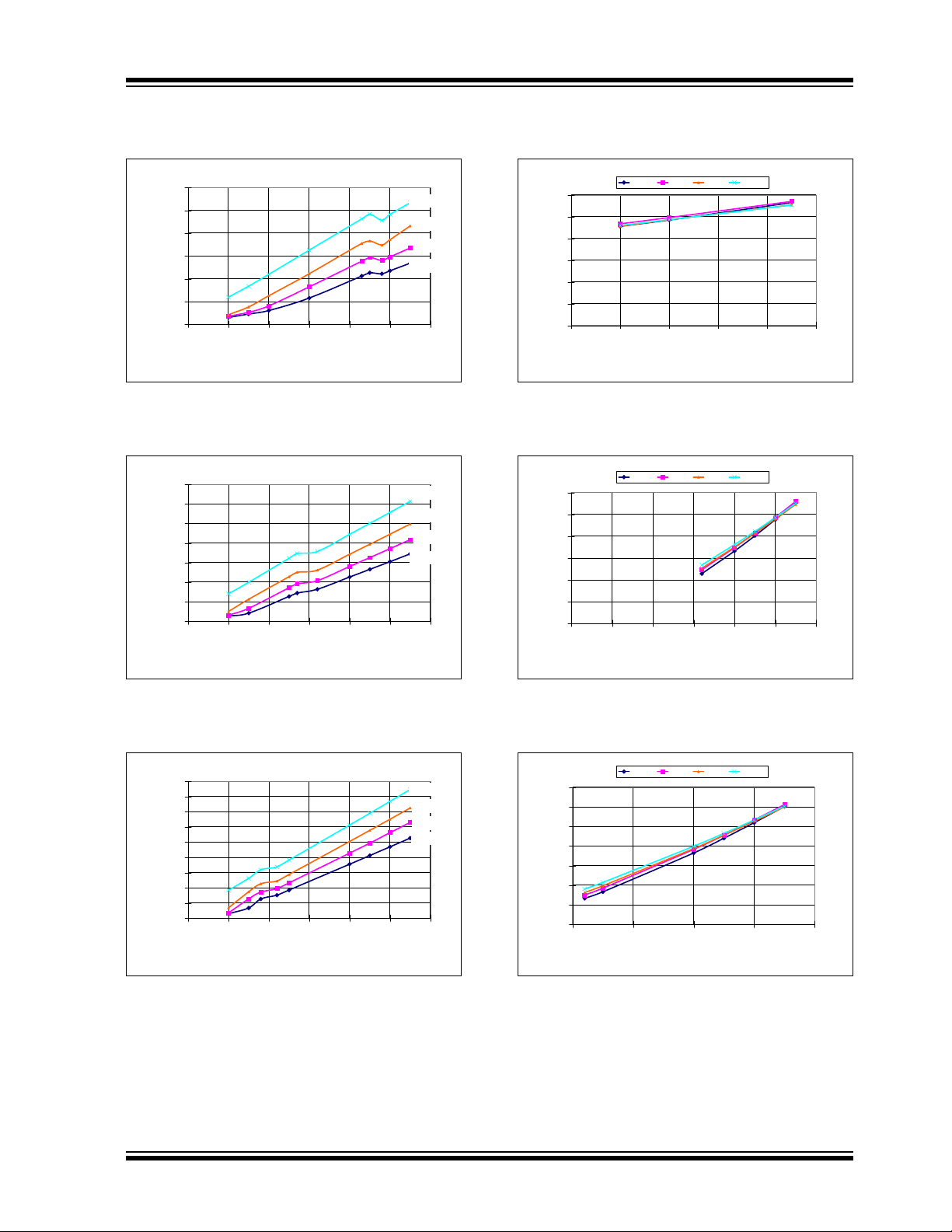
Note: Unless otherwise indicated, all limits are specified for VDD = 1V to 5.5V, RPU = 100 kΩ (only MCP1316;
see Figure 4-1), TA = -40°C to +125°C.
FIGURE 2-16: V
TRIP
and V
Temperature (MCP1318M-4.6).
FIGURE 2-17: V
TRIP
and V
Temperature (MCP1319-2.9).
HYST
HYST
vs.
vs.
FIGURE 2-19: V
(MCP1318M-4.6).
FIGURE 2-20: V
(MCP1319-2.9).
vs. IOL
OL
vs. IOL
OL
FIGURE 2-18: V
Temperature (MCP1316-2.0).
DS21985B-page 14 © 2007 Microchip Technology Inc.
TRIP
and V
HYST
vs.
FIGURE 2-21: V
(MCP1316-2.0).
vs. IOL
OL
Page 15
MCP131X/2X
0
0.02
0.04
0.06
0.08
0.1
0.12
0.14
-50 0 50 100 150
Temperature (°C)
V
OL
(V)
0.05 mA
0.1 mA
0.15 mA
0.2 mA
0
0.05
0.1
0.15
0.2
0.25
-50 0 50 100 150
Temperature (°C)
V
OL
(V)
0.05 mA
0.1 mA
0.15 mA
0.2 mA
0
0.002
0.004
0.006
0.008
0.01
0.012
0.014
0.016
-50 0 50 100 150
Temperature (°C)
V
OL
(V)
0.05 mA
0.1 mA
0.15 mA
0.2 mA
0
0.5
1
1.5
2
2.5
3
3.5
4
4.5
5
0.00 1.00 2.00 3.00 4.00 5.00 6.00
I
OH
(mA)
V
OH
(V)
1.5V
3V
4.5V
4.3V
2V
0
1
2
3
4
5
6
0.00 1.00 2.00 3.00 4.00 5.00 6.00
I
OH
(mA)
V
OH
(V)
1.5V
3.2V
2.7V
2.5V
5.5V
5V
4.5V
4V
0
1
2
3
4
5
6
0.00 1.00 2.00 3.00 4.00 5.00 6.00
I
OH
(mA)
V
OH
(V)
5.5V
5V
4.5V
4V
2.5V
2.2V
Note: Unless otherwise indicated, all limits are specified for VDD = 1V to 5.5V, RPU = 100 kΩ (only MCP1316;
see Figure 4-1), TA = -40°C to +125°C.
0 mA
FIGURE 2-22: VOL vs. Temperature
(MCP1318M-4.6 @ V
FIGURE 2-23: V
(MCP1319-2.9 @ V
= 4.5V).
DD
vs. Temperature
OL
= 2.7V).
DD
0 mA
FIGURE 2-25: V
OH
(MCP1318M-4.6 @ 25C).
FIGURE 2-26: V
OH
(MCP1319-2.9 @ 25C).
vs. IOH
vs. IOH
FIGURE 2-24: V
(MCP1316-2-0 @ V
© 2007 Microchip Technology Inc. DS21985B-page 15
DD
vs. Temperature
OL
= 1.8V).
0 mA
FIGURE 2-27: V
OH
(MCP1316-2.0 @ 25C).
vs. IOH
Page 16
MCP131X/2X
0
50
100
150
200
250
300
350
-100 -50 0 50 100 150
Temperature (°C)
t
RPD
(µs)
5V
5.5V
0
50
100
150
200
250
300
350
400
450
-100 -50 0 50 100 150
Temperature (°C)
t
RPD
(µs)
3.2V 4V 4.5V 5V 5.5V
0
50
100
150
200
250
300
350
-100 -50 0 50 100 150
Temperature (°C)
t
RPD
(µs)
2.5V 4V 4.5V 5V 5.5V
190
195
200
205
210
215
220
225
230
-100 -50 0 50 100 150
Temperature (°C)
t
RPU
(ms)
4.8 V 5 V 5.5 V
200
205
210
215
220
225
230
235
240
245
250
-100 -50 0 50 100 150
Temperature (°C)
t
RPU
(ms)
3.2 V 4 V 4.5 V 5 V 5.5 V
200
205
210
215
220
225
230
235
240
245
250
-100 -50 0 50 100 150
Temperature (°C)
t
RPU
(ms)
2.5 V 4 V 4.5 V 5 V 5.5 V 2.2 V
Note: Unless otherwise indicated, all limits are specified for VDD = 1V to 5.5V, RPU = 100 kΩ (only MCP1316;
see Figure 4-1), TA = -40°C to +125°C.
FIGURE 2-28: t
(MCP1318M-4.6).
FIGURE 2-29: t
(MCP1319-2.9).
vs. Temperature
RPD
vs. Temperature
RPD
FIGURE 2-31: t
(MCP1318M-4.6).
FIGURE 2-32: t
(MCP1319-2.9).
vs. Temperature
RPU
vs. Temperature
RPU
FIGURE 2-30: t
RPD
(MCP1316-2.0).
DS21985B-page 16 © 2007 Microchip Technology Inc.
vs. Temperature
FIGURE 2-33: t
(MCP1316-2.0).
vs. Temperature
RPU
Page 17
MCP131X/2X
0
500
1000
1500
2000
2500
3000
3500
0.001 0.01 0.1 1 10
Reset Threshold Over drive (V) V
TRIP
Min - V
Transient Duration (µs)
VRST=2.0V VRST=2.9V VRST=4.6V
2.0V
2.9V
0
0.002
0.004
0.006
0.008
0.01
0.012
-100 -50 0 50 100 150
Temperature (°C)
Open-Drain Leakage (µA)
2.2 V 2.5 V 4 V 4.5 V 5 V 5.5 V
MCP1318M does not
have a MR pin
0
50
100
150
200
250
300
350
-100 -50 0 50 100 150
Temperature (°C)
t
MRD
(ns)
3.2 V 4 V 4.5 V 5 V 5.5 V
0
50
100
150
200
250
300
350
400
450
-100 -50 0 50 100 150
Temperature (°C)
t
MRD
(ns)
2.2 V 2.5 V 4 V 4.5 V 5 V 5.5 V
Note: Unless otherwise indicated, all limits are specified for VDD = 1V to 5.5V, RPU = 100 kΩ (only MCP1316;
see Figure 4-1), TA = -40°C to +125°C.
DD
FIGURE 2-34: Transient Duration vs.
V
(min) – VDD.
TRIP
FIGURE 2-35: Open-Drain Leakage Current vs. Temperature (MCP1320-2.0).
FIGURE 2-37: MR
Low to Reset
Propagation Delay (MCP1319-2.9).
FIGURE 2-38: MR
Low to Reset
Propagation Delay (MCP1316-2.0).
FIGURE 2-36: MR
Propagation Delay (MCP1318M-4.6).
© 2007 Microchip Technology Inc. DS21985B-page 17
Low to Reset
Page 18
MCP131X/2X
0
100
200
300
400
500
600
700
800
900
1000
-100 -50 0 50 100 150
Temperature (°C)
t
RPD
(µs)
5V to 0V
5V to 4.5V
0
50
100
150
200
250
-100 -50 0 50 100 150
Temperature (°C)
t
RPD
(µs)
5V to 2.7V
5V to 0V
V
TRIP
V
TRIP
Min - 0.2V
0
50
100
150
200
250
-100 -50 0 50 100 150
Temperature (°C)
t
RPD
(µs)
5V to 0V
5V to 1.8V
V
TRIP
V
TRIP
Min - 0.2V
0.12
0.125
0.13
0.135
0.14
0.145
-100 -50 0 50 100 150
Temperature (°C)
Normalized Reset Timeout
Period
MCP1318M-4.6
0.125
0.13
0.135
0.14
0.145
0.15
-100 -50 0 50 100 150
Temperature (°C)
Normalized Reset Timeout
Period
MCP1319-2.9
0.125
0.13
0.135
0.14
0.145
0.15
-100 -50 0 50 100 150
Temperature (°C)
Normalized Reset Timeout
Period
MCP1316-2.0
Note: Unless otherwise indicated, all limits are specified for VDD = 1V to 5.5V, RPU = 100 kΩ (only MCP1316;
see Figure 4-1), TA = -40°C to +125°C.
FIGURE 2-39: VDD Falling to Reset Propagation Delay vs. Temperature (MCP1318M-4.6).
Typ + 0.3V to
FIGURE 2-40: V
Falling to Reset
DD
Propagation Delay vs. Temperature (MCP1319-
2.9).
FIGURE 2-42: Normalized Reset Time Out Period vs. Temperature (MCP1318M-4.6).
FIGURE 2-43: Normalized Reset Time Out Period vs. Temperature (MCP1319-2.9).
Typ + 0.2V to
FIGURE 2-41: V
Propagation Delay vs. Temperature (MCP1316-
2.0).
DS21985B-page 18 © 2007 Microchip Technology Inc.
Falling to Reset
DD
FIGURE 2-44: Normalized Reset Time Out Period vs. Temperature (MCP1316-2.0).
Page 19

MCP131X/2X
0.9
0.95
1
1.05
1.1
1.15
1.2
1.25
-100 -50 0 50 100 150
Temperature (°C)
Normalized Watchdog
Timeout Period
`
MCP1318M-4.6
MCP1319 does not
have a Watchdog Timer
0.9
0.95
1
1.05
1.1
1.15
1.2
1.25
-100 -50 0 50 100 150
Temperature (°C)
Normalized Watchdog
Timeout Period
`
MCP1316-2.0
0
100
200
300
400
500
600
0.001 0.01 0.1 1 10
Reset Threshold Overdrive (V) V
TRIP
Min - V
Transient Duration (µS)
VRST=2.0V VRST=2.9V VRST=4.6V
Note: Unless otherwise indicated, all limits are specified for VDD = 1V to 5.5V, RPU = 100 kΩ (only MCP1316;
see Figure 4-1), TA = -40°C to +125°C.
FIGURE 2-45: Normalized Watchdog Time Out Period vs. Temperature (MCP1318M-4.6).
FIGURE 2-48: Max VDD T ransient Duration vs. Reset Threshold Overdrive.
DD
FIGURE 2-46: Normalized Watchdog Time Out Period vs. Temperature (MCP1319-2.9).
FIGURE 2-47: Normalized Watchdog Time Out Period vs. Temperature (MCP1316-2.0).
© 2007 Microchip Technology Inc. DS21985B-page 19
FIGURE 2-49: “M” Part # Pull-up Characteristics (MCP1318M-4.6).
Page 20
MCP131X/2X
3.0 PIN DESCRIPTION
The descriptions of the pins are listed in Table 3-1.
TABLE 3-1: PIN FUNCTION TABLE
Pin No.
SOT23-5
1 MCP1316M
MCP1318M
MCP1319M
MCP1320,
MCP1321,
MCP1322
MCP1316,
MCP1318,
MCP1319
Device Symbol
(1)
,
RST
(1)
,
(1)
,
Pin
Type
O Open-Drain Reset Output (active-low)
OPush-PullV
Buffer/
Driver
Type
Function
Goes active (Low) if one of these conditions occurs:
1. If V
falls below the selected Reset voltage
DD
threshold.
2. If the MR
pin is forced low.
3. If the WDI pin does not de tect an edge transition
within the minimum selected time out period.
4. During power-up.
Falling:
V
DD
Open-Drain = VDD > V
L = V
DD
< V
TRIP
TRIP
VDD Rising:
Open-Drain = V
L = VDD < V
Falling:
DD
H = V
L = VDD < V
DD
> V
TRIP
TRIP
TRIP
DD
+ V
> V
HYS
TRIP
+ V
HYS
Rising:
V
DD
H = VDD > V
L = VDD < V
TRIP
TRIP
+ V
+ V
HYS
HYS
MCP1317 RST O Push-Pull Reset Output (active-high)
Goes active (High) if one of these conditions occurs:
1. If V
falls below the selected Reset voltage
DD
threshold.
2. If the MR
pin is forced low.
3. If the WDI pin does not de tect an edge transition
within the minimum selected time out period.
4. During power-up.
Falling:
V
DD
H = V
L = V
V
DD
H = V
L = V
< V
DD
> V
DD
Rising:
< V
DD
> V
DD
TRIP
TRIP
TRIP
TRIP
+ V
+ V
HYS
HYS
2AllVSS— P The ground reference for the device.
Note 1: Open-Drain output with internal pull-up resistor.
DS21985B-page 20 © 2007 Microchip Technology Inc.
Page 21

TABLE 3-1: PIN FUNCTION TABLE (CONTINUED)
Pin No.
SOT23-5
3 MCP1316,
Device Symbol
MR I ST Manual Reset input for a Reset switch.
Pin
Type
Buffer/
Driver
Type
MCP1316M,
MCP1317,
MCP1320
MCP1318,
RST O Push-Pull Reset Output (active-high)
MCP1318M,
MCP1319,
MCP1319M,
MCP1321,
MCP1322
MCP131X/2X
Function
This input allows a push button switch to be directly connected to the MCP131X/2X MR
used to force a system Reset. This input filters (ignores)
noise pulses that occur on the MR pin.
L = Switch is depressed (shorted to ground). This forces
the RST/RST
pins Active.
H = Switch is open (internal pull-up resistor pulls signal
high). State of the RST/RST
other system conditions.
Goes active (High) if one of these conditions occurs:
1. If V
falls below the selected Reset voltage
DD
threshold.
2. If the MR
pin is forced low.
3. If the WDI pin does not detect an edge transition
within the minimum selected time out period.
4. During power-up.
pin, which can then be
pins determined by
4 MCP1316,
WDI I ST Watchdog Timer Input
MCP1316M,
MCP1317,
MCP1318,
MCP1318M,
MCP1320,
MCP1321
MCP1319,
MR
I ST Manual Reset input for a Reset switch.
MCP1319M,
MCP1322
5AllV
DD
— P The positive supply for the device.
Note 1: Open-Drain output with internal pull-up resistor.
Falling:
V
DD
H = VDD < V
DD
> V
L = V
TRIP
TRIP
VDD Rising:
DD
< V
H = V
L = VDD > V
TRIP
TRIP
+ V
+ V
HYS
HYS
The WDT period is specified at the time of device order.
The Standard WDT period is 1.6s typical.
An edge transition on the WDI pin resets the Watchdog
Timer counter (no time out). A Falling Edge is required to
start the WDT Timer.
This input allows a push button switch to be directly connected to the MCP131X/2X MR
pin, which can then be
used to force a system Reset. This input filters (ignores)
noise pulses that occur on the MR
pin.
L = Switch is depressed (shorted to ground). This forces
the RST/RST
pins Active.
H = Switch is open (internal pull-up resistor pulls signal
high). State of the RST/RST pins determined by
other system conditions.
© 2007 Microchip Technology Inc. DS21985B-page 21
Page 22

MCP131X/2X
3.1 Ground Terminal (VSS)
VSS provides the negative reference for the analog
input voltage. Typically, the circuit ground is used.
3.2 Supply Voltage (VDD)
VDD can be used for power supply monitoring or a
voltage level that requires monitoring.
3.3 Reset Output (RST and RST)
There are four types of Reset output pins. These are:
1. Open-Drain active-low Reset, External pull-up
resistor required
2. Open-Drain active-low Reset, Internal pull-up
resistor
3. Push-Pull active-low Reset
4. Push-Pull active-high Reset
Some devices have both an active-low and active-high
Reset output.
3.3.1 ACTIVE-LOW (RST) - OPEN-DRAIN,
EXTERNAL PULL-UP RESISTOR
The RST open-drain output remains low while VDD is
below the Reset voltage threshold (V
device voltage (VDD) returns to a high level (V
V
), the device will remain in Reset for the Reset
HYS
delay timer (T
). After that time expires, the RST pin
RST
will float, and an external pull-up resistor is required to
bring the output to the high state.
). Once the
TRIP
TRIP
+
3.4 Manual Reset Input (MR)
The Manual Reset (MR) input pin allows a push button
switch to easily be connected to the system. When the
push button is depressed, it forces a system Reset.
This pin has circuitry that filters noise that may be
present on the MR
The MR
pin is active-low and has an internal pull-up
signal.
resistor.
3.5 Watchdog Input
In some systems, it is desirable to have an external
Watchdog Timer to monitor the operation of the system. This is done by requiring the embedded controller
to “pet” the Watchdog Timer within a predetermined
time frame (T
within this time frame, the MCP131X/2X will force the
Reset pin(s) active.
The embedded controller “pets” the MCP131X/2X by
forcing an edge transition on the WDI pin. The WDT
Timer is activated by the first falling edge on the WDI
pin.
The standard offering devices have a typical Watchdog
Timer period (T
able Watchdog Timer periods.
). If the MCP131X/2X is not “petted”
WD
) of 1.6 s. Table 1-3 shows the avail-
WD
3.3.2 ACTIVE-LOW (RST) - OPEN-DRAIN,
INTERNAL PULL-UP RESISTOR
The RST open-drain output remains low while VDD is
below the Reset voltage threshold (V
device voltage (VDD) returns to a high level (V
), the device will remain in Reset for the Reset
V
HYS
delay timer (T
). After that time expires, the RST pin
RST
). Once the
TRIP
TRIP
+
will be pulled high by an internal pull-up resistor (typically 4.7 kΩ).
3.3.3 ACTIVE-LOW (RST) - PUSH-PULL
The RST push-pull output remains low while VDD is
below the Reset voltage threshold (V
device voltage (V
), the device will remain in Reset for the Reset
V
HYS
delay timer (T
) returns to a high level (V
DD
). After that time expires, the RST pin
RST
). Once the
TRIP
TRIP
+
will be driven to the high state.
3.3.4 ACTIVE-HIGH (RST) - PUSH-PULL
The RST push-pull output remains high while VDD is
below the Reset voltage threshold (V
device voltage (V
), the device will remain in Reset for the Reset
V
HYS
delay timer (T
) returns to a high level (V
DD
). After that time expires, the RST pin
RST
will be driven to the low state.
). Once the
TRIP
TRIP
+
DS21985B-page 22 © 2007 Microchip Technology Inc.
Page 23

MCP131X/2X
V
DD
V
DD
MCLR
(Reset input)
(active-low)
V
SS
PIC
®
Microcontroller
R
PU
(1)
Note 1: Resistor RPU may be required with the
MCP1320, MCP1321, or MCP1322 due
to the open-drain output.
Resistor R
PU
may not be required with
the MCP1316M, MCP1318M, or
MCP1319M due to the internal pull-up
resistor.
The MCP1316, MCP1317, MCP1318,
and MCP1319 do not require the
external pull-up resistor.
2: Not all devices offer the active-high
Reset output pin.
0.1
µF
MCP13XX
V
DD
RST
V
SS
RST
(2)
WDI
I/O
To system
device that
requires activehigh resets
Push button
switch
MR
V
DD
Comparator
+
–
Output
Driver
RST
Reference
V
SS
RST
Noise Filter
Watchdog
MR
WDI
Note: Features available depend on the device.
Voltage
4.0 OPERATIONAL DESCRIPTION
For many of today’s microcontroller applications, care
must be taken to prevent low-power conditions that can
cause many different system problems. The most
common causes are brown-out conditions, where the
system supply drops below the operating level momentarily. The second most common cause is when a
slowly decaying power supply causes the
microcontroller to begin executing instructions without
sufficient voltage to sustain volatile memory (RAM),
thus producing indeterminate results. Figure 4-1 shows
a typical application circuit.
The MCP131X/2X family is voltage supervisor devices
designed to keep a microcontroller in Reset until the
system voltage has reached and stabilized at the
proper level for reliable system operation. These
devices also operate as protection from brown-out
conditions when the system supply voltage drops
below a safe operating level.
Some MCP131X/2X family members include a Watchdog Timer feature that after being enabled (by a falling
edge on the WDI pin), monitors the WDI pin for falling
edges. If an edge transition is not detected within the
expected timeframe, the MCP131X/2X devices will
force the Reset pin active. This is useful to ensure that
the embedded system’s Host Controller program is
operating as expected.
Some MCP131X/2X family members include a Manual
Reset feature that allows a push button switch to be
directly connected to the MCP131X/2X devices (on the
MR
the external control of the push button switch.
A superset block diagram is shown in Figure 4-2, with
device specific block diagrams shown in Figure 4-3
through Figure 4-12.
pin). This allows the system to easily be reset from
FIGURE 4-1: Typical Application Circuit.
© 2007 Microchip Technology Inc. DS21985B-page 23
FIGURE 4-2: Family Block Diagram
Page 24

MCP131X/2X
V
DD
Comparator
+
–
Output
Driver
RST
Reference
V
SS
Noise Filter
Watchdog
MR
WDI
Voltage
V
DD
Comparator
+
–
Output
Driver
RST
Reference
V
SS
Noise Filter
Watchdog
MR
WDI
Voltage
V
DD
Comparator
+
–
Output
Driver
Reference
V
SS
RST
Noise Filter
Watchdog
MR
WDI
Voltage
V
DD
Comparator
+
–
Output
Driver
RST
Reference
V
SS
RST
Watchdog
WDI
Voltage
V
DD
Comparator
+
–
Output
Driver
RST
Reference
V
SS
RST
Watchdog
WDI
Voltage
4.0.1 DEVICE SPECIFIC BLOCK
DIAGRAMS
FIGURE 4-3: MCP1316 Block Diagram.
FIGURE 4-4: MCP1316M Block Diagram.
FIGURE 4-6: MCP1318 Block Diagram.
FIGURE 4-7: MCP1318M Block Diagram.
FIGURE 4-5: MCP1317 Block Diagram.
DS21985B-page 24 © 2007 Microchip Technology Inc.
Page 25

MCP131X/2X
V
DD
Comparator
+
–
Output
Driver
RST
Reference
V
SS
RST
Noise Filter
MR
Voltage
V
DD
Comparator
+
–
Output
Driver
RST
Reference
V
SS
RST
Noise Filter
MR
Voltage
V
DD
Comparator
+
–
Output
Driver
RST
Reference
V
SS
Noise Filter
Watchdog
MR
WDI
Voltage
V
DD
Comparator
+
–
Output
Driver
RST
Reference
V
SS
RST
Watchdog
WDI
Voltage
V
DD
Comparator
+
–
Output
Driver
RST
Reference
V
SS
RST
Noise Filter
MR
Voltage
FIGURE 4-8: MCP1319 Block Diagram.
FIGURE 4-11: MCP1321 Block Diagram.
FIGURE 4-9: MCP1319M Block Diagram.
.
FIGURE 4-12: MCP1322 Block Diagram.
FIGURE 4-10: MCP1320 Block Diagram.
© 2007 Microchip Technology Inc. DS21985B-page 25
Page 26
MCP131X/2X
4.1 Reset Voltage Trip Point (V
TRIP
)
Operation
The device’s Reset voltage trip point (V
when the device is ordered. As the voltage on the
device’s V
pin is above or below this selected trip
DD
point, the output of the Reset pin (RST/RST ) will be
forced to either the inactive or active state.
For the voltage trip point, there is a minimum trip voltage
(V
) and a maximum trip voltage (V
TRIPMIN
) is selected
TRIP
TRIPMAX
). The
The Reset pin (RST or RST
of the following occurs:
• The Manual Reset input (MR
• The Watchdog Timer times out
goes below the threshold
•V
DD
• During device power-up
After the device exits the Reset condition, the delay
circuitry will hold the RST and RST
appropriate Reset delay time (t
) will be forced active if any
) goes low
pins active until the
) has elapsed.
RST
voltage that the device “actually” trip s at will be referred
to as V
. The trip voltage is specified for the falling of
TRIP
the device VDD.
There is also a hysteresis (V
) on the trip point. This
HYS
is so that noise on the device voltage (VDD) does not
cause the Reset pin (RST/RST
) to “jitter” (change
between driving an active and inactive state).
TABLE 4-1: RESET PIN STATES
State of RST Pin when: State of RST
Device
VDD <
V
TRIP
V
HYS
TRIP
+
VDD <
V
TRIP
V
>
DD
V
MCP1316 LH——Push-pull
MCP1316M LH
(2)
— — Open-drain
MCP1317 ——H LPush-pull
MCP1318 LHHLPush-pull
MCP1318M LH
(2)
H L Open-drain
MCP1319 LHHLPush-pull
MCP1319M LH
MCP1320 LH
MCP1321 LH
MCP1322 LH
(2)
H L Open-drain
(1)
— — Open-drain
(1)
H L Open-drain
(1)
H L Open-drain
Note 1: Requires External Pull-up resistor.
2: Has Internal Pull-up resistor.
3: The RST pin output is always push-pull.
(3)
Pin when:
V
>
DD
V
HYS
V
TRIP
+
Ouput Driver
(2)
(2)
(2)
(1)
(1)
(1)
DS21985B-page 26 © 2007 Microchip Technology Inc.
Page 27
MCP131X/2X
V
TRIPMAX
V
TRIPMIN
V
TRIP
1V
V
DD
V
TRIP
+ V
HYS
t
RST
RST
RST
VDD
V
TRIPMAX
V
TRIPMIN
V
TRIP
V
TRIP
V
TRIP
+ V
HYS
RST
1V
< 1V is outside the
device specifications
t
RPD
t
RST
t
RPD
t
RST
4.1.1 POWER-UP/RISING VDD
As the device VDD rises, the device’s Reset circuit will
remain active until the voltage rises above the “actual”
trip point (V
) plus the hysteresis (V
TRIP
Figure 4-13 shows a power-up sequence and the
waveform of the RST and RST
pins.
As the device powers up, the voltage will start below
the valid operating voltage of the device. At this voltage, the Reset output value is not valid. Once the voltage is above the minimum operating voltage (1V) and
below the selected V
, the Reset output will be
TRIP
active.
Once the device voltage rises above the “actual” trip
point (V
timer (t
) plus the hysteresis (V
TRIP
) starts. When the Reset delay timer times
RST
HYS
out, the Reset output (RST/RST) is driven inactive.
Note: While the Reset delay timer (t
active, additional system current is consumed.
).
HYS
), the Reset delay
) is
RST
4.1.2 POWER-DOWN/BROWN-OUTS
As the device powers-down/brown-outs, the voltage
) falls from a voltage above the devices trip point
(V
DD
(V
). The devices “actual” trip point voltage (V
TRIP
will be between the minimum trip point (V
the maximum trip point (V
TRIPMAX
). Once the device
TRIPMIN
TRIP
) and
voltage (VDD) goes below this voltage, the Reset pin(s)
will be forced to the active state. There is a hysteresis
on this trip point. This is so that noise on the device voltage (V
) does not cause the Reset pin (RST/RST) to
DD
“jitter” (change between driving an active and inactive).
Figure 4-14 shows the waveform of the RST
pin as
determined by the VDD voltage, while Table 4-1 shows
the state of the RST pin.
4.1.2.1 Operation of RST pin with Internal
Pull-Up Resistor
Note: Only the MCP1316M, MCP1318M, and
MCP1319M devices have an open-drain
RST output pin with an internal pull-up
resistor.
The internal pull-up resistor has a typical value of
4.7 kΩ. The internal pull-up eliminates the need for an
external resistor.
To reduce the current consumption of the device, when
the RST
pin is driving low, the resistor is disconnected.
)
FIGURE 4-13: Reset pin Operation on a Power-up.
FIGURE 4-14: RST Operation as determined by the V
© 2007 Microchip Technology Inc. DS21985B-page 27
TRIP
and V
HYS
.
Page 28

MCP131X/2X
V
TRIP
V
DD
RST
t
RST
Reset Delay
Timer Inactive
Reset
Delay
Timer
Inactive
Reset Delay
Timer Active
See Figures 2-12,
2-10 and 2-11
See Figures 2-15,
2-14 and 2-13
See Figures 2-12,
2-10 and 2-11
4.2 Reset Delay Timer (t
RST
)
The Reset delay timer ensures that the MCP131X/2X
device will “hold” the embedded system in Reset until
the system voltage has stabilized. There are several
time-out options to better meet the requirements of
different applications. These Reset delay timer time
outs are shown in Table 4-2. The S tandard offering time
out is typically 200 ms.
The Reset delay timer (t
age rises above the “actual” trip point (V
hysteresis (V
). When the Reset delay timer times
HYS
out, the Reset output pin (RST/RST
Note: While the Reset delay timer (t
) starts after the device volt-
RST
TRIP
) plus the
) is driven inactive.
RST
) is
active, additional system current is consumed.
TABLE 4-2: RESET DELAY TIMER
TIME OUTS
t
RST
(1)
Units
Min Typ Max
1.0 1.4 2.0 ms
20 30 40 ms
140 200 280 ms
1120 1.6 2.24 sec
↑↑
This is the minimum time that the
Reset delay timer
will “hold” the
Reset pin active
after VDD rises
above
+ V
V
TRIP
HYS
This is the maxi-
mum time that the
Reset delay timer
will “hold” the
Reset pin active
DD
rises
after V
above
+ V
V
TRIP
HYS
Note 1: Shaded rows are custom ordered time
outs.
Figure 4-15 illustrates when the Reset delay timer
(t
) is active or inactive.
RST
FIGURE 4-15: Reset Power-up Timer Waveform.
4.2.1 EFFECT OF TEMPERATURE ON
RESET POWER-UP TIMER (T
The Reset delay timer time out period (t
determines how long the device remains in the Reset
condition. This time out is affected by both the device
and temperature. Typical responses for different
V
DD
VDD values and temperatures are shown in Figures 233, 2-32 and 2-31.
RPU
)
RST
)
DS21985B-page 28 © 2007 Microchip Technology Inc.
Page 29
MCP131X/2X
Time (µs)
0V
Supply Voltage
5V
V
TRIP(MIN)
- V
DD
t
TRANS
V
TRIP(MAX)
V
TRIP(MIN)
(Overdrive)
(Duration)
V
DD
MR
V
SS
RST
WDI
I/O
MCLR
+5V
MCP13XX
PIC® MCU
RST
V
IL
t
MR
RST
t
MRD
V
IH
t
RST
MR
The MR input typically ignores input pulses
of 100 ns.
4.3 Negative Going VDD Transients
The minimum pulse width (time) required to cause a
Reset may be an important criteria in the implementation of a Power-on Reset (POR) circuit. This time is
referred to as transient duration. The MCP131X/2X
devices are designed to reject a level of negative-going
transients (glitches) on the power supply line.
Transient duration is the amount of time needed for
these supervisory devices to respond to a drop in V
The transient duration time (t
magnitude of V
– VDD (overdrive). Any combination
TRIP
) is dependant on the
TRAN
of duration and overdrive that lies under the durati on/
overdrive curve will not generate a Reset signal. Generally speaking, the transient duration time decreases
with and increases in the V
– VDD voltage. Combi-
TRIP
nations of duration and overdrive that lies above the
duration/overdrive curve are detected as a brown-out
or power-down condition.
Figure 4-16 shows a typical transient duration vs.
Reset comparator overdrive, for which the MCP131X/
2X will not generate a Reset pulse. It shows that the farther below the trip point the transient pulse goes, the
duration of the pulse required to cause a Reset gets
shorter. Figure 4-16 shows the transient response
characteristics for the MCP131X/2X.
Transient immunity can be improved by adding a
bypass capacitor (typically 0.1 µF) as close as possible
to the V
pin of the MCP131X/2X device.
DD
DD
4.4 Manual Reset Input
The Manual Reset input pin (MR) allows the Reset pins
(RST/RST
The MR pin has circuitry to filter noise pulses that may
be present on the pin. Figure 4-17 shows a block dia-
gram for using the MCP131X/2X with a push button
switch. To minimize the required external components,
the MR
.
A mechanical push button or active logic signal can
drive the MR
Once MR
Reset delay time), the Reset output pins are forced
active. The Reset output pins will remain in their active
states for the Reset delay timer time out period (t
Figure 4-18 shows a waveform for the Manual Reset
switch input and the Reset pins output.
) to be manually forced to their active states.
input has an internal pull-up resistor.
input.
has been low for a time, t
(the Manual
MRD
RST
)
FIGURE 4-16: Example of Typical Transient Duration Waveform.
© 2007 Microchip Technology Inc. DS21985B-page 29
FIGURE 4-17: Push Button Reset and Watchdog Timer.
FIGURE 4-18: MR
Input – Push Button.
4.4.1 NOISE FILTER
The noise filter filters out noise spikes (glitches) on the
Manual Reset pin (MR
(typical) are filtered.
). Noise spikes less than 100 ns
Page 30

MCP131X/2X
V
CC
GND
RST
WDI
MCLR
+5V
MCP13XX
0.1
10 kΩ
I/O
PIC
®
3-Terminal
Regulator
+5V
µF
MCU
(example:
MCP1700)
4.5 Watchdog Timer
The purpose of the Watchdog Timer (WDT) is to
Figure 4-19 shows a block diagram for using the
MCP131X/2X with a PIC
®
microcontroller (MCU) and
the Watchdog input.
increase system reliability. The Watchdog Timer feature can be used to detect when the Host Controller ’s
program flow is not as expected. The Watchdog Timer
monitors for activity on the Watchdog Input pin (WDI).
The WDI pin is expected to be strobed within a given
time frame. When this time frame is exceeded, without
an edge transition on the WDI pin, the Reset pin is
driven active to reset the system. This stops the Host
Controller from continuing its erratic behavior (“runaway” code execution).
The Watchdog Timer is external to the main portion of
the control system and monitors the operation of the
system. This feature is enabled by a falling edge on the
WDI pin (after device POR). Monitoring is then done by
requiring the embedded controller to force an edge
transition (falling or rising) on the WDI pin (“pet the
Watchdog”) within a predetermined time frame (T
WD
If the MCP131X/2X does not detect an edge on the
WDI pin within the expected time frame, the MCP131X/
2X device will force the Reset pin active.
The Watchdog Timer is in the disabled state when:
• The Device Powers up
• A POR event occurred
• A WDT event occurred
• A Manual Reset (MR
) event occurred
When the Watchdog Timer is in the disabled state, the
).
TABLE 4-3: WATCHDOG TIMER
PERIODS
t
WDT
(1)
Units
Min Typ Max
4.3 6.3 9.3 ms
71 102 153 ms
1.12 1.6 2.4 sec
17.9 25.6 38.4 sec
↑↑
If the time between
WDI edges is less
than this, it
ensures that the
MCP131X/2X
never forces a
reset
If the time
between WDI
edges is greater
than this, it
ensures that the
MCP131X/2X
always forces a
reset
Note 1: Shaded rows are custom ordered Watch-
dog Timer Periods (t
) time outs. For
WDT
information on ordering devices with
these t
time outs, please contact your
WDT
local Microchip sales office. Minimum
purchase volumes are required.
WDI pin has an internal smart pull-up resistor enabled.
This pull-up resistor has a typical value of 52 kΩ. This
pull-up resistor holds the WDI signal in the high state,
until it is forced to another state.
After the embedded controller has initialized, if the
Watchdog Timer feature is to be used, then the embedded controller can force the WDI pin low (V
). This also
IL
enables the Watchdog Timer feature and disables the
WDI pull-up resistor. Disabling the pull-up resistor
reduces the device’s current consumption. The pull-up
resistor will remain disconnected until the device has a
power-on, a Reset event occurs, or after the WDT time
out.
Once the Watchdog Timer has been enabled, the Host
Contoller must force an edge transition (falling or rising)
on the WDI pin before the minimum Watchdog Timer
time out to ensure that the Watchdog Timer does not
force the Reset pins (RST/RST
) to the active state.
If an edge transition does not occur before the maximum time out occurs, then the MCP131X/2X will force
the Reset pins to their active state.
The MCP131X/2X supports four time outs. The stan-
FIGURE 4-19: Watchdog Timer.
The software routine that strobes WDI is critical. The
code must be in a section of software that is executed
frequently enough so the time between edge transitions is less than the Watchdog time out period. One
common technique controls the Host Controllers I/O
line from two sections of the program. The software
might set the I/O line high while operating in the Foreground mode and set it low while in the Background or
Interrupt modes. If both modes do not execute correctly, the Watchdog Timer issues reset pulses.
dard offering devices have a typical Watchdog Timer
period (T
Watchdog Timer periods. The t
function of the device voltage and temperature.
DS21985B-page 30 © 2007 Microchip Technology Inc.
) of 1.6 s. Table 4-3 shows the available
WDT
WDT
time out is a
Page 31
MCP131X/2X
MCP131X/2X
V
DD
RST
V
SS
0.1 µF
RST
WDI
MR
V
DD
RST
V
SS
BATLOW
MCP131X/2X
+
––
V
DD
RST
V
SS
Power Good
MCP131X/2X
+
–
Pwr
Sply
MCP132X
V
DD
VDD/V
PP
V
DD
RST
MCLR
Reset input)
(Active-Low)
V
SS
V
SS
PIC
®
Microcontroller
R
PU
0.1 µF
1kΩ
5.0 APPLICATION INFORMATION
This section shows application related information that
may be useful for your particular design requirements.
5.1 Supply Monitor Noise Sensitivity
The MCP131X/2X devices are optimized for fast
response to negative-going changes in V
with an inordinate amount of electrical noise on V
(such as systems using relays) may require a 0.01 µF
or 0.1 µF bypass capacitor to reduce detection sensitivity. This capacitor should be installed as close to the
MCP131X/2X as possible to keep the capacitor lead
length short.
FIGURE 5-1: Typical Application Circuit with Bypass Capacitor.
. Systems
DD
DD
5.3 Using in PIC® Microcontroller, ICSP™ Applications
Note: This operation can only be done using the
device with the Open-Drain RST
(MCP1320, MCP1321, and MCP1322).
Devices that have the internal pull-up
resistor are not recommended due to the
current path of the internal pull-up resistor.
Figure 5-4 shows the typical application circuit for using
the MCP132X for voltage superviory function when the
PIC microcontroller will be programmed via the In-Circuit Serial Programming™ (ICSP™) feature. Additional
information is available in TB087, “Using Voltage
Supervisors with PIC
Implement In-Circuit Serial Programming™”,
DS91087.
Note: It is recommended that the current into the
RST pin be current limited by a 1 kΩ
resistor.
®
Microcontroller Systems which
pin
5.2 Conventional Voltage Monitoring
Figure 5-2 and Figure 5-3 show the MCP131X/2X in
conventional voltage monitoring applications.
FIGURE 5-2: Battery Voltage Monitor.
FIGURE 5-3: Power Good Monitor.
© 2007 Microchip Technology Inc. DS21985B-page 31
FIGURE 5-4: Typical Application Circuit
for PIC
®
Microcontroller with the ICSP™
Feature.
Page 32
MCP131X/2X
Note: In this example, V
SOURCE
must be
greater than (V
TRIP
)
MCP131X/2X
V
DD
RST
V
SS
R
1
V
SOURCE
R
2
or RST
V
SOURCE
R
1
R1R2+
------------------- -
× V
TRIP
=
Where:
V
SOURCE
= Voltage to be monitored
V
TRIP
= Threshold Voltage setting
V
DD
RST
V
SS
MCP131X/2X
270Ω
MTP3055EL
V
DD
R
L
V
TRIP
5.4 Modifying The Trip Point, V
TRIP
Although the MCP131X/2X device has a fixed voltage
trip point (V
), it is sometimes necessary to make
TRIP
custom adjustments. This can be accomplished by
connecting an external resistor divider to the
MCP131X/2X V
pin. This causes the V
DD
SOURCE
voltage to be at a higher voltage than when the MCP131X/
2X input equals its V
voltage (Figure 5-5).
TRIP
To maintain detector accuracy, the bleeder current
through the divider should be significantly higher than
the 10 µA maximum operating current required by the
MCP131X/2X. A reasonable value for this bleeder
current is 1 mA (100 times the 10 µA required by the
MCP131X/2X). For example, if V
desired trip point is 2.5V , the value of R
= 2V and the
TRIP
+ R2 is 2.5 kΩ
1
(2.5V/1 mA). The value of R1 + R2 can be rounded to
the nearest standard value and plugged into the equation of Figure 5-5 to calculate values for R
and R2. 1%
1
tolerance resistors are recommended.
5.5 MOSFET Low-Drive Protection
Low operating power and small physical size make the
MCP131X/2X series ideal for many voltage detector
applications. Figure 5-6 shows a low-voltage gate drive
protection circuit that prevents overheating of the logiclevel MOSFET due to insufficient gate voltage. When
the input signal is below the threshold of the MCP131X/
2X, its output grounds the gate of the MOSFET.
FIGURE 5-6: MOSFET Low-Drive Protection.
5.6 Low-Power Applications
FIGURE 5-5: Modify Trip-Point using External Resistor Divider.
DS21985B-page 32 © 2007 Microchip Technology Inc.
In some low-power applications, the longer that the
microcontroller (such as a PIC MCU) can be in the
“Sleep mode”, the lower the average system current
consumption will be.
The WDT feature can be used to “wake-up” the PIC MCU
at a regular interval to service the required tasks before
returning to sleep. This “wake-up” occurs after the PIC
MCU detects a MCLR
reset during Sleep mode (for mid-
range family; POR = ‘1’, BOR = ‘1’, TO = ‘1’, and PD = ‘1’).
Page 33

MCP131X/2X
MCP13XX
V
DD
RST
GND
MCLR
GND
Buffered Reset
To Other System
Components
MCU
4.7 kΩ
Buffer
PIC
®
MCP13XX
V
DD
V
DD
R
1
100 kΩ
RST
GND
5.7 Controllers and Processors With Bidirectional I/O Pins
Some microcontrollers have bidirectional Reset pins.
Depending on the current drive capability of the controller pin, an indeterminate logic level may result if there
is a logic conflict. This can be avoided by adding a
4.7 kΩ resistor in series with the output of the
MCP131X/2X (Figure 5-7). If there are other components in the system that require a Reset signal, they
should be buffered so as not to load the Reset line. If
the other components are required to follow the Reset
I/O of the microcontroller, the buffer should be connected as shown with the solid line.
5.8 RESET Signal Integrity During Power-Down
The MCP131X/2X Reset output is valid to VDD = 1.0V.
Below this 1.0V, the output becomes an "open circuit"
and does not sink or source current. This means
CMOS logic inputs to the microcontroller will be floating
at an undetermined voltage. Most digital systems are
completely shut down well above this voltage.
However, in situations where the Reset signal must be
maintained valid to V
required.
For devices where the Reset signal is active-low, a pulldown resistor must be connected from the MCP131X/
2X Reset pin(s) to ground to discharge stray capacitances and hold the output low (Figure 5-8).
Similarly for devices where the Reset signal is activehigh, a pull-up resistor to V
valid high Reset signal for V
This resistor value, though not critical, should be
chosen such that it does not appreciably load the Reset
pin(s) under normal operation (100 kΩ will be suitable
for most applications).
= 0V, external circuitry is
DD
is required to ensure a
DD
below 1.0V.
DD
FIGURE 5-7: Interfacing the MCP131X/ 2X Push-Pull outputs to a Bidirectional Reset I/O.
FIGURE 5-8: Ensuring a valid active-low
Reset pin output state as V
approaches 0V.
DD
© 2007 Microchip Technology Inc. DS21985B-page 33
Page 34
MCP131X/2X
6.0 STANDARD DEVICE OFFERINGS
Table 7-1 shows the standard devices that are avail-
able and their respective configuration. The configuration includes the:
RST
TRIP
)
WDT
)
)
• Voltage Trip Point (V
• Reset Time Out (t
• Watchdog Time Out (t
Table 7-1 also shows the order number for that given
device configuration.
7.0 CUSTOM CONFIGURATIONS
Table 7-2 shows the codes that specify the desired
Reset time out (t
) for custom devices.
(t
WDT
The voltage trip point (V
digits of the desired typical trip point voltage. As an
example, if the desired V
V
of 2.7V, the code is 27.
TRIP
) and Watchdog Timer time out
RST
) is specified by the two
TRIP
selection has a typical
TRIP
TABLE 7-1: STANDARD VERSIONS
Device
MCP1316 2.90 140 200 1.12 1.6 MCP1316T-29LE/OT
MCP1316 4.60 140 200 1.12 1.6 MCP1316T-46LE/OT
MCP1316M 2.90 140 200 1.12 1.6 MCP1316MT-29LE/OT
MCP1316M 4.60 140 200 1.12 1.6 MCP1316MT-46LE/OT
MCP1317 2.90 140 200 1.12 1.6 MCP1317T-29LE/OT
MCP1317 4.60 140 200 1.12 1.6 MCP1317T-46LE/OT
MCP1318 2.90 140 200 1.12 1.6 MCP1318T-29LE/OT
MCP1318 4.60 140 200 1.12 1.6 MCP1318T-46LE/OT
MCP1318M 2.90 140 200 1.12 1.6 MCP1318MT-29LE/OT
MCP1318M 4.60 140 200 1.12 1.6 MCP1318MT-46LE/OT
MCP1319 2.90 140 200 — — MCP1319T-29LE/OT
MCP1319 4.60 140 200 — — MCP1319T-46LE/OT
MCP1319M 2.90 140 200 — — MCP1319MT-29LE/OT
MCP1319M 4.60 140 200 — — MCP1319MT-46LE/OT
MCP1320 2.90 140 200 1.12 1.6 MCP1320T-29LE/OT
MCP1320 4.60 140 200 1.12 1.6 MCP1320T-46LE/OT
MCP1321 2.90 140 200 1.12 1.6 MCP1321T-29LE/OT
MCP1321 4.60 140 200 1.12 1.6 MCP1321T-46LE/OT
MCP1322 2.90 140 200 — — MCP1322T-29LE/OT
MCP1322 4.60 140 200 — — MCP1322T-46LE/OT
Reset
Threshold (V)
Reset Time Out (ms) Watchdog Time Out (s)
Minimum Typical Minimum Typical Order Number
TABLE 7-2: DELAY TIME OUT ORDERING CODES
T ypical Delay Time (ms) T ypical Delay Time (ms)
Code Reset WDT Comment Code Reset WDT Comment
A 1.6 6.3 Note 1 J 200.0 6.3 Note 1
B 1.6 102.0 Note 1 K 200.0 102.0 Note 1
C 1.6 1600.0 Note 1 L 200.0 1600.0 Delay timings for standard
device offerings
D 1.6 25600.0 Note 1 M 200.0 25600.0 Note 1
E 30.0 6.3 Note 1 N 1600.0 6.3 Note 1
F 30.0 102.0 Note 1 P 1600.0 102.0 Note 1
G 30.0 1600.0 Note 1 Q 1600.0 1600.0 Note 1
H 30.0 25600.0 Note 1 R 1600.0 25600.0 Note 1
Note 1: This delay timing combination is not the standard offering. For information on ordering devices with these
delay times, contact your local Microchip sales office. Minimum purchase volumes are required.
DS21985B-page 34 © 2007 Microchip Technology Inc.
Page 35

8.0 DEVELOPMENT TOOLS
8.1 Evaluation/Demonstration Boards
The SOT-23-5/6 Evaluation Board (VSUPEV2) can be
used to evaluate the characteristics of the MCP131X/
2X devices.
This blank PCB has footprints for:
• Pull-up Resistor
• Pull-down Resistor
• Loading Capacitor
• In-line Resistor
There is also a power supply filtering capacitor.
For evaluating the MCP131X/2X devices, the selected
device should be installed into the Option A footprint.
MCP131X/2X
FIGURE 1: SOT-23-5/6 Voltage
Supervisor Evaluation Board (VSUPEV2).
This board may be purchased directly from the
Microchip web site at www.microchip.com.
© 2007 Microchip Technology Inc. DS21985B-page 35
Page 36

MCP131X/2X
5-Pin SOT-23
Part Number SOT-23
MCP1316T-29LE/OT QANN
MCP1316MT-29LE/OT QBNN
MCP1317T-29LE/OT QCNN
MCP1318T-29LE/OT QDNN
MCP1318MT-29LE/OT QENN
MCP1319T-29LE/OT QFNN
MCP1319MT-29LE/OT QGNN
MCP1320T-29LE/OT QHNN
MCP1321T-29LE/OT QJNN
MCP1322T-29LE/OT QKNN
MCP1316T-46LE/OT QLNN
MCP1316MT-46LE/OT QMNN
MCP1317T-46LE/OT QPNN
MCP1318T-46LE/OT QQNN
MCP1318MT-46LE/OT QRNN
MCP1319T-46LE/OT QSNN
MCP1319MT-46LE/OT QTNN
MCP1320T-46LE/OT QUNN
MCP1321T-46LE/OT QVNN
MCP1322T-46LE/OT QWNN
Example:
Legend: XX...X Customer-specific information
Y Year code (last digit of calendar year)
YY Year code (last 2 digits of calendar year)
WW Week code (week of January 1 is week ‘01’)
NNN Alphanumeric traceability code
Pb-free JEDEC designator for Matte Tin (Sn)
* This package is Pb-free. The Pb-free JEDEC designator ( )
can be found on the outer packaging for this package.
Note: In the event the full Microchip part number cannot be marked on one line, it will
be carried over to the next line, thus limiting the number of available
characters for customer-specific information.
XXNN QANN
9.0 PACKAGING INFORMATION
9.1 Package Marking Information
3
e
3
e
DS21985B-page 36 © 2007 Microchip Technology Inc.
Page 37

MCP131X/2X
/HDG3ODVWLF6PDOO2XWOLQH7UDQVLVWRU27>627@
1RWHV
'LPHQVLRQV'DQG(GRQRWLQFOXGHPROGIODVKRUSURWUXVLRQV0ROGIODVKRUSURWUXVLRQVVKDOOQRWH[FHHGPPSHUVLGH
'LPHQVLRQLQJDQGWROHUDQFLQJSHU$60(<0
%6& %DVLF'LPHQVLRQ7KHRUHWLFDOO\H[DFWYDOXHVKRZQZLWKRXWWROHUDQFHV
1RWH )RUWKHPRVWFXUUHQWSDFNDJHGUDZLQJVSOHDVHVHHWKH0LFURFKLS3DFNDJLQJ6SHFLILFDWLRQORFDWHGDW
KWWSZZZPLFURFKLSFRPSDFNDJLQJ
8QLWV 0,//,0(7(56
'LPHQVLRQ/LPLWV 0,1 120 0$;
1XPEHURI3LQV 1
/HDG3LWFK H %6&
2XWVLGH/HDG3LWFK H %6&
2YHUDOO+HLJKW $ ±
0ROGHG3DFNDJH7KLFNQHVV $ ±
6WDQGRII $ ±
2YHUDOO:LGWK ( ±
0ROGHG3DFNDJH:LGWK ( ±
2YHUDOO/HQJWK ' ±
)RRW/HQJWK / ±
)RRWSULQW / ±
)RRW$QJOH ±
/HDG7KLFNQHVV F ±
/HDG:LGWK E ±
φ
N
b
E
E1
D
1
2
3
e
e1
A
A1
A2
c
L
L1
0LFURFKLS 7HFKQRORJ\ 'UDZLQJ &%
© 2007 Microchip Technology Inc. DS21985B-page 37
Page 38

MCP131X/2X
Top
Cover
Tape
K
0
P
W
B
0
A
0
User Direction of Feed
P, Pitch
Standard Reel Component Orientation
Reverse Reel Component Orientation
W, Width
of Carrier
Tape
Pin 1
Pin 1
Device
Marking
9.2 Product Tape and Reel Specifications
FIGURE 9-1: EMBOSSED CARRIER DIMENSIONS (8 MM TAPE ONLY)
TABLE 1: CARRIER TAPE/CAVITY DIMENSIONS
Case
Outline
Package
Type
Carrier
Dimensions
W
mmPmm
mm
Dimensions
A0
Cavity
B0
mm
K0
mm
Output
Quantity
Units
OT SOT-23 3L 8 4 3.2 3.2 1.4 3000 180
FIGURE 9-2: 5-LEAD SOT-23 DEVICE TAPE AND REEL SPECIFICATIONS
Reel
Diameter in
mm
DS21985B-page 38 © 2007 Microchip Technology Inc.
Page 39

APPENDIX A: REVISION HISTORY
Revision B (October 2007)
• Clarified that devices with a Voltage Trip Point
≤ 2.4V are tested from -40°C to + 85°C. Devices
with a Voltage Trip Point ≥ 2.5V are tested from
°C to +125°C.
-40
Revision A (November 2005)
• Original Release of this Document.
MCP131X/2X
© 2007 Microchip Technology Inc. DS21985B-page 39
Page 40

MCP131X/2X
NOTES:
DS21985B-page 40 © 2007 Microchip Technology Inc.
Page 41

MCP131X/2X
Device: MCP1316T: MicroPower Voltage Detector
(Tape and Reel)
MCP1316MT: MicroPower Voltage Detector
(Tape and Reel)
MCP1317T: MicroPower Voltage Detector
(Tape and Reel)
MCP1318T: MicroPower Voltage Detector
(Tape and Reel)
MCP1318MT: MicroPower Voltage Detector
(Tape and Reel)
MCP1319T: MicroPower Voltage Detector
(Tape and Reel)
MCP1319MT: MicroPower Voltage Detector
(Tape and Reel)
MCP1320T: MicroPower Voltage Detector
(Tape and Reel)
MCP1321T: MicroPower Voltage Detector
(Tape and Reel)
MCP1322T: MicroPower Voltage Detector
(Tape and Reel)
V
TRIP
Options:
(Note 1)
29 = 2.90V
46 = 4.60V
Time Out Options:
(Note 1)
L=t
RST
= 200 ms (typ),
t
WDT
= 1.6 s (typ)
Temperature Range: I = -40°C to +85°C
(Only for trip points 2.0V to 2.4V)
E = -40°C to +125°C
(For trip point ≥ 2.5V)
Package: OT = SOT-23, 5-lead
Note 1: Custom ordered voltage trip points and time outs available. Please
contact your local Microchip sales office for additional information.
Minimum purchase volumes are required.
PART NO. XX X
Temperature
V
TRIP
Options
Device
Examples:
a) MCP1316T-29LE/OT: 5-Lead SOT-23-5
b) MCP1316T-46LE/OT: 5-Lead SOT-23-5
c) MCP1316MT-29LE/OT: 5-Lead SOT-23-5
d) MCP1316MT-46LE/OT: 5-Lead SOT-23-5
a) MCP1317T-29LE/OT: 5-Lead SOT-23-5
b) MCP1317T-46LE/OT: 5-Lead SOT-23-5
a) MCP1318T-29LE/OT: 5-Lead SOT-23-5
b) MCP1318MT-29LE/OT: 5-Lead SOT-23-5
c) MCP1318T-46LE/OT: 5-Lead SOT-23-5
d) MCP1318MT-46LE/OT: 5-Lead SOT-23-5
a) MCP1319T-29LE/OT: 5-Lead SOT-23-5
b) MCP1318MT-29LE/OT: 5-Lead SOT-23-5
c) MCP1319T-46LE/OT: 5-Lead SOT-23-5
d) MCP1318MT-46LE/OT: 5-Lead SOT-23-5
a) MCP1320T-29LE/OT: 5-Lead SOT-23-5
b) MCP1320T-46LE/OT: 5-Lead SOT-23-5
a) MCP1321T-29LE/OT: 5-Lead SOT-23-5
b) MCP1321T-46LE/OT: 5-Lead SOT-23-5
a) MCP1322T-29LE/OT: 5-Lead SOT-23-5
b) MCP1322T-46LE/OT: 5-Lead SOT-23-5
Range
X
X
Package
X
Tape/Reel
Option
/
X
Time Out
Options
PRODUCT IDENTIFICATION SYSTEM
To order or obtain information, e.g., on pricing or delivery, refer to the factory or the listed sales office.
© 2007 Microchip Technology Inc. DS21985B-page 41
Page 42

MCP131X/2X
NOTES:
DS21985B-page 42 © 2007 Microchip Technology Inc.
Page 43

Note the following details of the code protection feature on Microchip devices:
• Microchip products meet the specification contained in their particular Microchip Data Sheet.
• Microchip believes that its family of products is one of the most secure families of its kind on the market today, when used in the
intended manner and under normal conditions.
• There are dishonest and possibly illegal methods used to breach the code protection feature. All of these methods, to our
knowledge, require using the Microchip products in a manner outside the operating specifications contained in Microchip’s Data
Sheets. Most likely, the person doing so is engaged in theft of intellectual property.
• Microchip is willing to work with the customer who is concerned about the integrity of their code.
• Neither Microchip nor any other semiconductor manufacturer can guarantee the security of their code. Code protection does not
mean that we are guaranteeing the product as “unbreakable.”
Code protection is constantly evolving. We at Microchip are committed to continuously improving the code protection features of our
products. Attempts to break Microchip’s code protection feature may be a violation of the Digital Millennium Copyright Act. If such acts
allow unauthorized access to your software or other copyrighted work, you may have a right to sue for relief under that Act.
Information contained in this publication regarding device
applications and the like is provided only for your convenience
and may be superseded by updates. It is your responsibility to
ensure that your application meets with your specifications.
MICROCHIP MAKES NO REPRESENTATIONS OR
WARRANTIES OF ANY KIND WHETHER EXPRESS OR
IMPLIED, WRITTEN OR ORAL, STATUTORY OR
OTHERWISE, RELATED TO THE INFORMATION,
INCLUDING BUT NOT LIMITED TO ITS CONDITION,
QUALITY, PERFORMANCE, MERCHANTABILITY OR
FITNESS FOR PURPOSE. Microchip disclaims all liability
arising from this information and its use. Use of Microchip
devices in life support and/or safety applications is entirely at
the buyer’s risk, and the buyer agrees to defend, indemnify
and hold harmless Microchip from any and all damages,
claims, suits, or expenses resulting from such use. No
licenses are conveyed, implicitly or otherwise, under any
Microchip intellectual property rights.
Trademarks
The Microchip name and logo, the Microchip logo, Accuron,
dsPIC, K
EELOQ, KEELOQ logo, microID, MPLAB, PIC,
PICmicro, PICSTART, PRO MATE, rfPIC and SmartShunt are
registered trademarks of Microchip Technology Incorporated
in the U.S.A. and other countries.
AmpLab, FilterLab, Linear Active Thermistor, Migratable
Memory, MXDEV, MXLAB, SEEVAL, SmartSensor and The
Embedded Control Solutions Company are registered
trademarks of Microchip Technology Incorporated in the
U.S.A.
Analog-for-the-Digital Age, Application Maestro, CodeGuard,
dsPICDEM, dsPICDEM.net, dsPICworks, dsSPEAK, ECAN,
ECONOMONITOR, FanSense, FlexROM, fuzzyLAB,
In-Circuit Serial Programming, ICSP, ICEPIC, Mindi, MiWi,
MPASM, MPLAB Certified logo, MPLIB, MPLINK, PICkit,
PICDEM, PICDEM.net, PICLAB, PICtail, PowerCal,
PowerInfo, PowerMate, PowerTool, REAL ICE, rfLAB, Select
Mode, Smart Serial, SmartTel, Total Endurance, UNI/O,
WiperLock and ZENA are trademarks of Microchip
Technology Incorporated in the U.S.A. and other countries.
SQTP is a service mark of Microchip Technology Incorporated
in the U.S.A.
All other trademarks mentioned herein are property of their
respective companies.
© 2007, Microchip Technology Incorporated, Printed in the
U.S.A., All Rights Reserved.
Printed on recycled paper.
Microchip received ISO/TS-16949:2002 certification for its worldwide
headquarters, design and wafer fabrication facilities in Chandler and
T empe, Arizona; Gresham, Oregon and design centers in California
and India. The Company’s quality system processes and procedures
are for its PIC
devices, Serial EEPROMs, microperipherals, nonvolatile memory and
analog products. In addition, Microchip’s quality system for the desig n
and manufacture of development systems is ISO 9001:2000 certified.
®
MCUs and dsPIC® DSCs, KEELOQ
®
code hopping
© 2007 Microchip Technology Inc. DS21985B-page 43
Page 44

WORLDWIDE SALES AND SERVICE
AMERICAS
Corporate Office
2355 West Chandler Blvd.
Chandler, AZ 85224-6199
Tel: 480-792-7200
Fax: 480-792-7277
Technical Support:
http://support.microchip.com
Web Address:
www.microchip.com
Atlanta
Duluth, GA
Tel: 678-957-9614
Fax: 678-957-1455
Boston
Westborough, MA
Tel: 774-760-0087
Fax: 774-760-0088
Chicago
Itasca, IL
Tel: 630-285-0071
Fax: 630-285-0075
Dallas
Addison, TX
Tel: 972-818-7423
Fax: 972-818-2924
Detroit
Farmington Hills, MI
Tel: 248-538-2250
Fax: 248-538-2260
Kokomo
Kokomo, IN
Tel: 765-864-8360
Fax: 765-864-8387
Los Angeles
Mission Viejo, CA
Tel: 949-462-9523
Fax: 949-462-9608
Santa Clara
Santa Clara, CA
Tel: 408-961-6444
Fax: 408-961-6445
Toronto
Mississauga, Ontario,
Canada
Tel: 905-673-0699
Fax: 905-673-6509
ASIA/PACIFIC
Asia Pacific Office
Suites 3707-14, 37th Floor
Tower 6, The Gateway
Harbour City, Kowloon
Hong Kong
Tel: 852-2401-1200
Fax: 852-2401-3431
Australia - Sydney
Tel: 61-2-9868-6733
Fax: 61-2-9868-6755
China - Beijing
Tel: 86-10-8528-2100
Fax: 86-10-8528-2104
China - Chengdu
Tel: 86-28-8665-5511
Fax: 86-28-8665-7889
China - Fuzhou
Tel: 86-591-8750-3506
Fax: 86-591-8750-3521
China - Hong Kong SAR
Tel: 852-2401-1200
Fax: 852-2401-3431
China - Nanjing
Tel: 86-25-8473-2460
Fax: 86-25-8473-2470
China - Qingdao
Tel: 86-532-8502-7355
Fax: 86-532-8502-7205
China - Shanghai
Tel: 86-21-5407-5533
Fax: 86-21-5407-5066
China - Shenyang
Tel: 86-24-2334-2829
Fax: 86-24-2334-2393
China - Shenzhen
Tel: 86-755-8203-2660
Fax: 86-755-8203-1760
China - Shunde
Tel: 86-757-2839-5507
Fax: 86-757-2839-5571
China - Wuhan
Tel: 86-27-5980-5300
Fax: 86-27-5980-5118
China - Xian
Tel: 86-29-8833-7252
Fax: 86-29-8833-7256
ASIA/PACIFIC
India - Bangalore
Tel: 91-80-4182-8400
Fax: 91-80-4182-8422
India - New Delhi
Tel: 91-11-4160-8631
Fax: 91-11-4160-8632
India - Pune
Tel: 91-20-2566-1512
Fax: 91-20-2566-1513
Japan - Yokohama
Tel: 81-45-471- 6166
Fax: 81-45-471-6122
Korea - Daegu
Tel: 82-53-744-4301
Fax: 82-53-744-4302
Korea - Seoul
Tel: 82-2-554-7200
Fax: 82-2-558-5932 or
82-2-558-5934
Malaysia - Kuala Lumpur
Tel: 60-3-6201-9857
Fax: 60-3-6201-9859
Malaysia - Penang
Tel: 60-4-227-8870
Fax: 60-4-227-4068
Philippines - Manila
Tel: 63-2-634-9065
Fax: 63-2-634-9069
Singapore
Tel: 65-6334-8870
Fax: 65-6334-8850
Taiwan - Hsin Chu
Tel: 886-3-572-9526
Fax: 886-3-572-6459
Taiwan - Kaohsiung
Tel: 886-7-536-4818
Fax: 886-7-536-4803
Taiwan - Taipei
Tel: 886-2-2500-6610
Fax: 886-2-2508-0102
Thailand - Bangkok
Tel: 66-2-694-1351
Fax: 66-2-694-1350
EUROPE
Austria - Wels
Tel: 43-7242-2244-39
Fax: 43-7242-2244-393
Denmark - Copenhagen
Tel: 45-4450-2828
Fax: 45-4485-2829
France - Paris
Tel: 33-1-69-53-63-20
Fax: 33-1-69-30-90-79
Germany - Munich
Tel: 49-89-627-144-0
Fax: 49-89-627-144-44
Italy - Milan
Tel: 39-0331-742611
Fax: 39-0331-466781
Netherlands - Drunen
Tel: 31-416-690399
Fax: 31-416-690340
Spain - Madrid
Tel: 34-91-708-08-90
Fax: 34-91-708-08-91
UK - Wokingham
Tel: 44-118-921-5869
Fax: 44-118-921-5820
10/05/07
DS21985B-page 44 © 2007 Microchip Technology Inc.
 Loading...