

Page 1
M
Low Noise, Positive-Regulated Charge Pump
MCP1252/3
Features
• Inductorless, Buck/Boost, DC/DC Converter
• Low Power: 80 µA (Typical)
• High Output Voltage Accuracy:
- ±2.5% (V
• 120 mA Output Current
• Wide Operating Temperature Range:
- -40°C to +85°C
• Thermal Shutdown and Short-Circuit Protection
• Uses Small Ceramic Capacitors
• Switching Frequency:
- MCP1252: 650 kHz
- MCP1253: 1 MHz
• Low Power Shutdown Mode: 0.1 µA (Typical)
• Shutdown Input Compatible with 1.8V Logic
Range: 2.0V to 5.5V
•V
IN
• Selectable Output Voltage (3.3V or 5.0V) or
Adjustable Output Voltage
• Space-saving, 8-Lead MSOP
• Soft-Start Circuitry to Minimize In-Rush Current
OUT
Fixed)
Applications
• White LED Backlighting
• Color Display Bias
• Local 3V-to-5V Conversions
• Flash Memory Supply Voltage
• SIM Interface Supply for GSM Phones
• Smart Card Readers
• PCMCIA Local 5V Supplies
Description
The MCP1252/3 are inductorless, positive-regulated
charge pump DC/DC converters. The devices generate
a regulated fixed (3.3V or 5.0V) or adjustable output
voltage. They are specifically designed for applications
requiring low noise and high efficiency and are able to
deliver up to 120 mA output current. The devices allow
the input voltage to be lower or higher than the output
voltage, by automatically switching between buck/
boost operation.
The MCP1252 has a switching frequency of 650 kHz,
avoiding interference with sensitive IF bands. The
MCP1253 has a switching frequency of 1 MHz and
allows the use of smaller capacitors than the
MCP1252, thus saving board space and cost.
Both devices feature a power-good output that can be
used to detect out-of-regulation conditions. Extremely
low supply current and low external parts count (three
capacitors) make these devices ideal for small, batterypowered applications. A shutdown mode is also provided for further power reduction. The MCP1252 and
MCP1253 feature thermal and short-circuit protection
and are offered in space-saving, 8-lead, MSOP
packages.
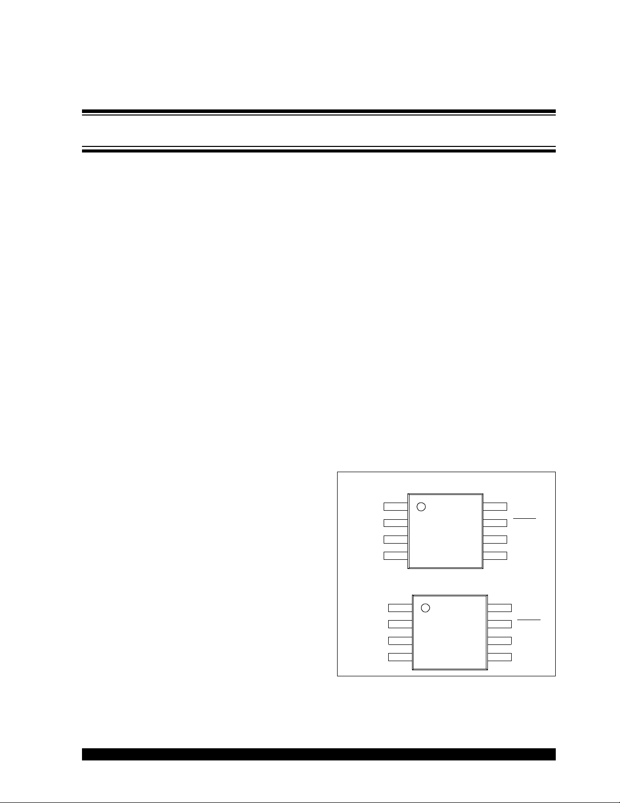
Package Types
MSOP (FIXED)
PGOOD
V
OUT
V
GND
1
MCP1252
2
MCP1253
IN
3
4
8
7
6
5
SELECT
SHDN
C+
C-
MSOP (ADJUSTABLE)
PGOOD
V
OUT
V
IN
GND
2002 Microchip Technology Inc. DS21752A-page 1
1
2
MCP1252
3
MCP1253
4
8
7
6
5
FB
SHDN
C+
C-
Page 2
MCP1252/3
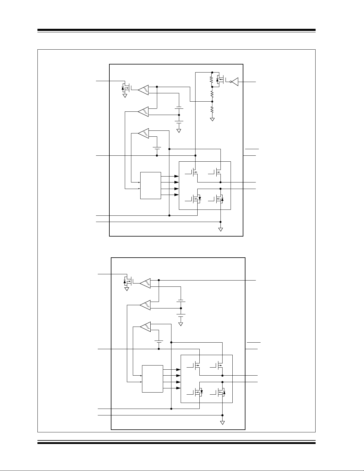
Functional Block Diagram
MCP1252-33X50
MCP1253-33X50
PGOOD
V
OUT
V
GND
+
+
84 mV
-
1.21V
+
-
Switch
Control
+
200 mV
IN
140 kΩ
173 kΩ
+
100 kΩ
+
SELECT
SHDN
C+
C-
MCP1252-ADJ
MCP1253-ADJ
PGOOD
V
OUT
V
GND
+
+
84 mV
-
+
-
Switch
Control
+
200 mV
IN
1.21V
+
+
FB
SHDN
C+
C-
DS21752A-page 2 2002 Microchip Technology Inc.
Page 3
MCP1252/3
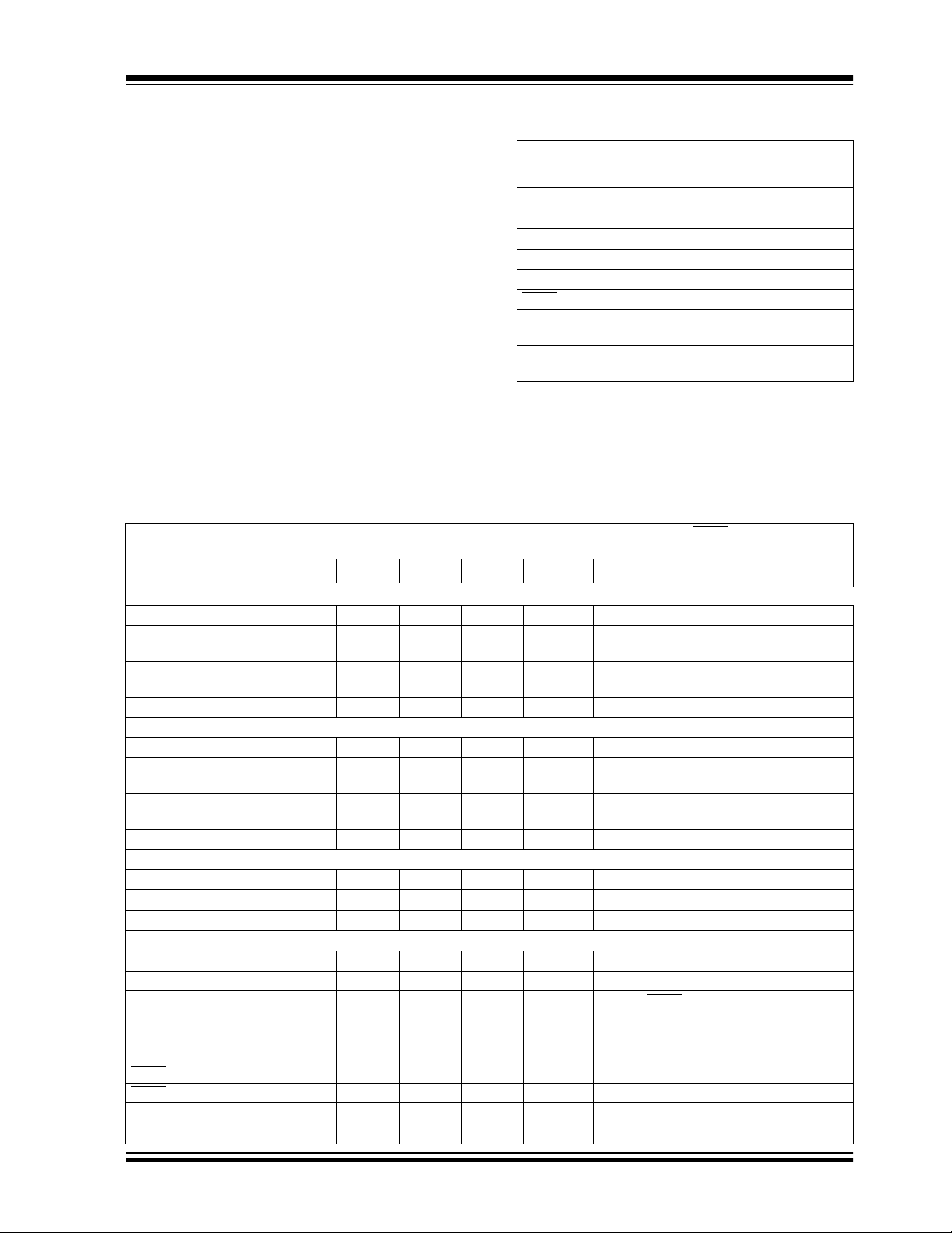
1.0 ELECTRICAL CHARACTERISTICS
Absolute Maximum Ratings †
Power Supply Voltage, VIN...............................................6.0V
Voltage on Any Pin w.r.t. GND ............... -0.3V to (V
Output Short Circuit Duration ................................continuous
Storage Temperature Range.........................-65°C to +150°C
Ambient Temperature with Power Applied....-55°C to +125°C
Junction Temperature ................................................. +150°C
ESD Ratings:
Human Body Model (1.5 kΩ in Series with 100 pF ...... ≥ 4kV
Machine Body Model (200 pF, No Series Resistance ≥ 400V
+ 0.3V)
IN
PIN FUNCTION TABLE
Name Function
PGOOD Open-Drain Power GOOD Output
V
OUT
V
IN
GND Ground Terminal
C- Flying Capacitor Negative Terminal
C+ Flying Capacitor Positive Terminal
SHDN
SELECT
FB
Regulated Output Voltage
Power Supply Input
Shutdown Mode, Active-Low Input
Output Voltage Select Pin.
(MCP1252-33X50, MCP1253-33X50)
Feedback Input Pin for Adjustable Output
(MCP1252-ADJ, MCP1253-ADJ)
†Notice: Stresses above those listed under “Maximum Ratings” may cause permanent damage to the device. This is a
stress rating only and functional operation of the device at
those or any other conditions above those indicated in the
operational listings of this specification is not implied. Exposure to maximum rating conditions for extended periods may
affect device reliability.
ELECTRICAL CHARACTERISTICS
Electrical Specifications: Unless otherwise specified, all limits are specified for TA = -40°C to +85°C, SHDN = VIN,
C
= C
OUT
= 10 µF, C
IN
Parameters Sym Min Typ Max Units Conditions
Selectable Output - MCP1252-33X50, MCP1253-33X50: SELECT = V
Supply Voltage V
Output Voltage Accuracy V
Output Current I
SELECT Logic Input Voltage High V
Selectable Output - MCP1252-33X50, MCP1253-33X50: SELECT = GND, V
Supply Voltage V
Output Voltage Accuracy V
Output Current I
SELECT Logic Input Voltage Low V
Adjustable Output - MCP1252-ADJ, MCP1253-ADJ
Supply Voltage V
Output Voltage Adjustment Range V
FB Regulation Voltage V
ALL DEVICES
Supply Current I
Output Short-Circuit Current I
Shutdown Current I
Power Efficiency η —8168—%%V
Logic Input Voltage Low V
SHDN
Logic Input Voltage High V
SHDN
PGOOD Threshold Voltage V
PGOOD Hysteresis V
FLY
= 1 µF, I
= 10 mA. Typical values are for TA = +25°C.
OUT
IN
OUT
OUT
IH
IN
OUT
OUT
IL
IN
OUT
FB
DD
SC
SHDN
IL
IH
TH
HYS
2.1 — 5.5 V
-2.5 +/-0.5 +2.5 % 2.3V ≤ VIN < 2.5V, I
80
120
100
150
1.4 — — V MCP1252-33X50, MCP1253-33X50
2.7 — 5.5 V
-2.5 +/-0.5 +2.5 % 2.7V ≤ V
40
120
80
150
— — 0.4 V MCP1252-33X50, MCP1253-33X50
2.0 — 5.5 V
1.5 — 5.5 V V
1.18 1.21 1.24 V MCP1252-ADJ, MCP1253-ADJ
—60120µANo load
—200 —mAV
— 0.1 2.0 µA SHDN = 0V
—— 0.4V
1.4 — — V
—0.93V
—0.04V
OUT
OUT
, V
OUT
= 3.3V
IN
2.5V ≤ V
—mAmA2.3V ≤ VIN < 2.5V
2.5V ≤ V
= 5.0V
OUT
3.0V ≤ V
—mAmA2.7V ≤ VIN < 3.0V
3.0V ≤ V
OUT(MAX)
OUT
= 3.0V, V
IN
V
= 3.6V, V
IN
I
OUT
—V
—V
≤ 5.5V, I
IN
≤ 5.5V
IN
< 3.0V, I
IN
≤ 5.5V, I
IN
≤ 5.5V
IN
< 2 x V
= GND, foldback current
OUT
OUT
=120 mA
OUT
OUT
OUT
OUT
IN
= 5V
= 5V
≤ 80 mA
≤ 120 mA
≤ 40 mA
≤ 120 mA
2002 Microchip Technology Inc. DS21752A-page 3
Page 4
MCP1252/3
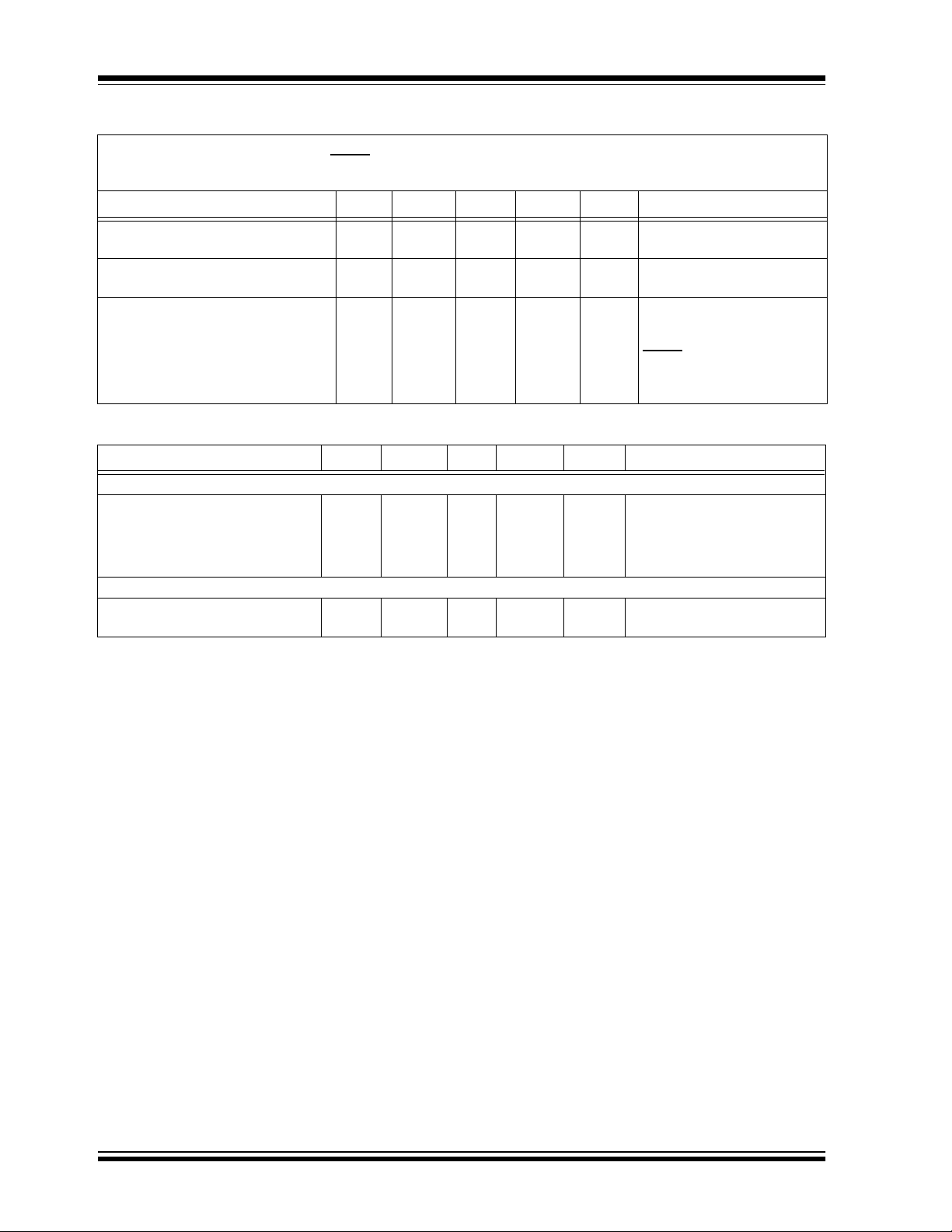
AC CHARACTERISTICS
Electrical Specifications: Unless otherwise specified, all limits are specified for T
V
= 2.7V to 5.5V, SELECT = GND, SHDN = VIN, C
IN
Typical values are for T
= +25°C.
A
IN
= C
OUT
= 10 µF, C
FLY
= 1 µF, I
Parameters Sym Min Typ Max Units Conditions
Internal Oscillator Frequency F
Ripple Voltage V
V
Wake-Up Time From Shutdown T
OUT
OSC
RIP
WKUP
520
800
—5045—mV
—200
650
1000
780
1200
—µsec
300
TEMPERATURE SPECIFICATIONS
Parameters Symbol Min Typ Max Units Conditions
Temperature Ranges:
Specified Temperature Range T
Maximum Operating Junction
Temperature
Storage Temperature Range T
Thermal Package Resistances:
Thermal Resistance, 8 Pin MSOP θ
A
T
J
A
JA
-40 — +85 °C
— — +125 °C
-65 — +150 °C
— 206 — °C/W Single-Layer SEMI G42-88
= -40°C to +85°C,
A
= 10 mA.
OUT
kHz
MCP1252
kHz
MCP1253
MCP1252
p-p
p-p
MCP1253
mV
SELECT = V
µsec
SELECT = GND
V
= 3.6V, I
IN
SHDN
= V
V
from 0 to 90% Nominal
OUT
Regulated Output Voltage
Board, Natural Convection
IN
OUT
IH(MIN)
= 10 mA,
,
DS21752A-page 4 2002 Microchip Technology Inc.
Page 5
MCP1252/3
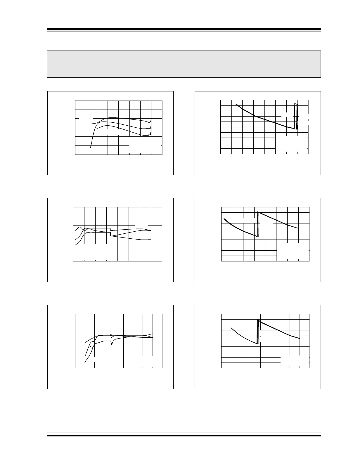
2.0 TYPICAL PERFORMANCE CURVES
Note: The graphs and tables provided following this note are a statistical summary based on a limited number of
samples and are provided for informational purposes only. The performance characteristics listed herein
are not tested or guaranteed. In some graphs or tables, the data presented may be outside the specified
operating range (e.g., outside specified power supply range) and therefore outside the warranted range.
Note: Unless otherwise indicated, V
= 3.6V, TA = 25°C, CIN = C
IN
= 10µF, C
OUT
= 1µF, all capacitors X7R ceramic.
FLY
5.05
5.04
10 mA
5.03
5.02
80 mA 120 mA
5.01
Output Voltage (V)
5.00
4.99
2.0 2.5 3.0 3.5 4.0 4.5 5.0 5.5 6.0
Supply Voltage (V)
MCP125 2-33X50
SELECT = GND
OUT
= 5.0V
V
FIGURE 2-1: Output Voltage vs. Supply Voltage (MCP1252-33X50).
.
3.34
3.33
3.32
Output Voltage (V)
MCP125 2-33X50
SELECT = V
V
3.31
OUT
2.0 2.5 3.0 3.5 4.0 4.5 5.0 5.5 6.0
IN
= 3.3V
Supply Voltage (V)
80 mA
120 mA
10 mA
100
90
80
70
60
50
40
30
20
Percent Efficiency (%)
10
0
2.0 2.5 3.0 3.5 4.0 4.5 5.0 5.5 6.0
Supply Voltage (V)
10 mA
80 mA
120 mA
MCP125 2-33X50
SELECT = GND
= 5.0V
V
OUT
FIGURE 2-4: Percent Efficiency vs. Supply Voltage (MCP1252-33X50).
100
90
80
70
60
50
40
30
20
Power Efficiency (%)
10
0
2.0 2.5 3.0 3.5 4.0 4.5 5.0 5.5 6.0
10 mA
80 mA
120 mA
Supply Voltage (V)
MCP125 2-33X50
SELECT = V
V
= 3.3V
OUT
IN
FIGURE 2-2: Output Voltage vs. Supply Voltage (MCP1252-33X50).
3.02
3.01
10 mA
3.00
Output Voltage (V)
2.99
1.5 2.0 2.5 3.0 3.5 4.0 4.5 5.0 5.5 6.0
80 mA
120 mA
Supply Voltage (V)
MCP125 2-ADJ
= 3.0V
V
OUT
FIGURE 2-3: Output Voltage vs. Supply Voltage (MCP1252-ADJ).
FIGURE 2-5: Power Efficiency vs. Supply Voltage (MCP1252-33X50).
100
90
80
70
60
50
40
30
20
Power Efficiency (%)
10
0
1.5 2.0 2.5 3.0 3.5 4.0 4.5 5.0 5.5 6.0
10 mA
80 mA
120 mA
Supply Voltage (V)
MCP125 2-ADJ
= 3.0V
V
OUT
FIGURE 2-6: Power Efficiency vs. Supply
Voltage
(MCP1252-ADJ).
2002 Microchip Technology Inc. DS21752A-page 5
Page 6

MCP1252/3
Note: Unless otherwise indicated, V
5.03
5.02
5.01
5.00
Output Voltage (V)
4.99
4.98
MCP125 3-33X50
MCP125 2-33X50
-40 -25 -10 5 20 35 50 65 80 95 110 125
Temperature (°C)
= 3.6V, TA = 25°C, CIN = C
IN
SELECT = GND
= 5.0V
V
OUT
I
= 120 mA
OUT
FIGURE 2-7: Output Voltage vs. Temperature (MCP1252-33X50, MCP1253-33X50).
3.33
3.32
3.31
3.30
3.29
Output Voltage (V)
3.28
MCP125 3-33X50
MCP125 2-33X50
SELECT = V
V
= 3.3V
OUT
I
= 120 mA
OUT
-40 -25 -10 5 20 35 50 65 80 95 110 125
Temperature (°C)
= 10 mF, C
OUT
80
75
70
65
60
55
50
Supply Current (uA)
45
40
-40 -25 -10 5 20 35 50 65 80 95 110 125
= 1 mF, all capacitors X7R ceramic.
FLY
VIN = 5.5V
VIN = 3.6V
VIN = 2.7V
VIN = 2.3V
Temperature (°C)
MCP1253-33X50
SELECT = GND
V
= 5.0V, I
OUT
OUT
= 0 mA
FIGURE 2-10: Quiescent Current vs. Temperature (MCP1253-33X50).
80
VIN = 5.5V
75
70
65
60
IN
55
50
Supply Current (uA)
45
40
VIN = 3.6V
VIN = 2.7V
VIN = 2.3V
-40 -25 -10 5 20 35 50 65 80 95 110 125
Temperature (°C)
MCP1252-33X50
SELECT = GND
V
= 5.0V, I
OUT
OUT
= 0 mA
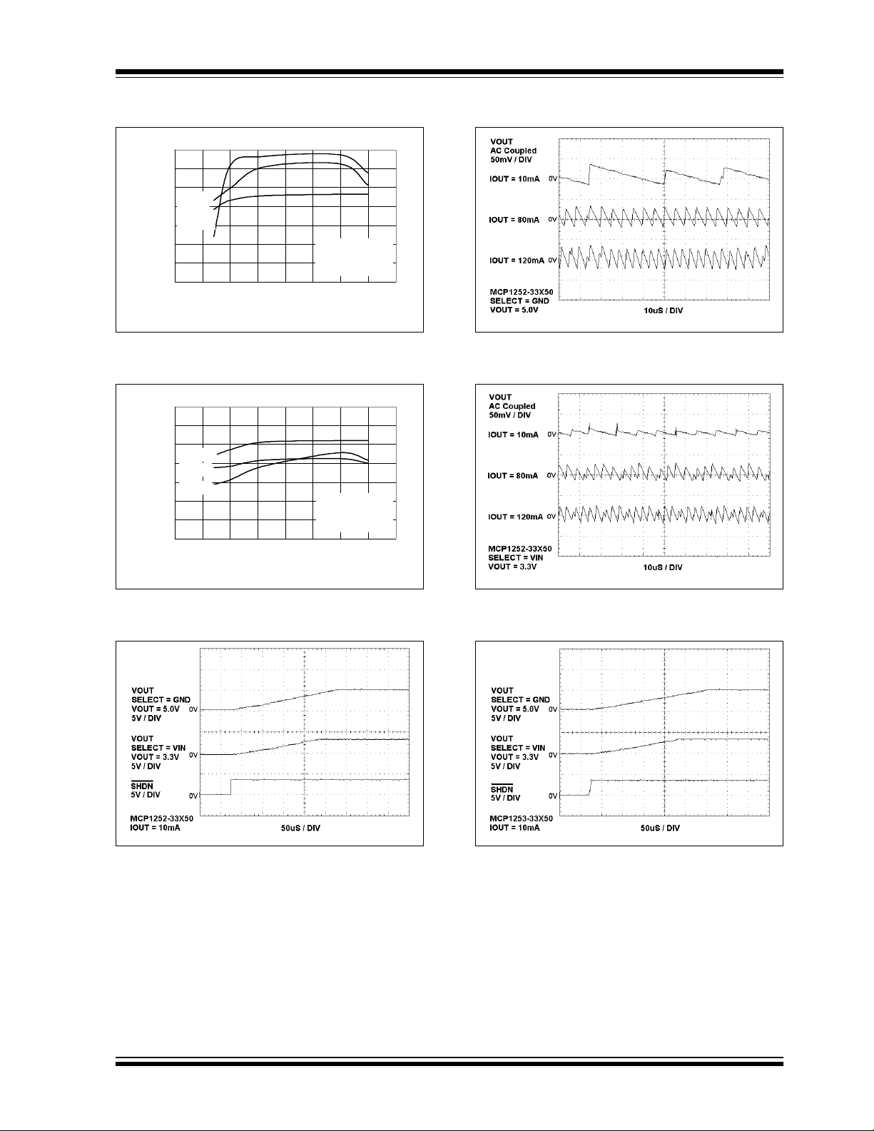
FIGURE 2-8: Output Voltage vs. Temperature (MCP1252-33X50, MCP1253-33X50).
FIGURE 2-9: Line Transient Response.
FIGURE 2-11: Quiescent Current vs.
Temperature (MCP1252-33X50).
FIGURE 2-12: Load Transient Response.
DS21752A-page 6 2002 Microchip Technology Inc.
Page 7
MCP1252/3
Note: Unless otherwise indicated, V
70
60
50
80 mA
40
10 mA
120 mA
30
20
10
Output Voltage Ripple (mV)
0
2.0 2.5 3.0 3.5 4.0 4.5 5.0 5.5 6.0
Supply Voltage (V)
= 3.6V, TA = 25°C, CIN = C
IN
MCP125 2-33X50
SELECT = GND
= 5.0V
V
OUT
FIGURE 2-13: Output Voltage Ripple vs. Supply Voltage (MCP1252-33X50).
70
60
50
120 mA
40
80 mA
30
10 mA
20
10
Output Voltage Ripple (mV)
0
2.0 2.5 3.0 3.5 4.0 4.5 5.0 5.5 6.0
Supply Voltage (V)
MCP125 2-33X50
SELECT = V
V
OUT
= 3.3V
IN
= 10mF, C
OUT
= 1mF, all capacitors X7R ceramic.
FLY
FIGURE 2-16: Output Voltage Ripple vs. Time.
FIGURE 2-14: Output Voltage Ripple vs. Supply Voltage (MCP1252-33X50).
FIGURE 2-15: Start-Up (MCP1252-33X50).
FIGURE 2-17: Output Voltage Ripple vs.
Time.
FIGURE 2-18: Start-Up (MCP1253-33X50).
2002 Microchip Technology Inc. DS21752A-page 7
Page 8

MCP1252/3
3.0 PIN FUNCTIONS
TABLE 3-1: PIN FUNCTION TABLE
Pin
No.
3.1 Open-Drain Power Good Output
PGOOD is a high-impedance when the output voltage
is in regulation. A logic-low is asserted when the output
falls 7% (typical) below the nominal value. The PGOOD
output remains low until V
its nominal value. On start-up, this pin indicates when
the output voltage reaches its final value. PGOOD is
high-impedance when SHDN
Name Function
1 PGOOD
2V
3V
4GND
5C-
6C+
7 SHDN
8 SELECT
Open-Drain Power GOOD Output
Regulated Output Voltage
OUT
Power Supply Input
IN
Ground Terminal
Flying Capacitor Negative Terminal
Flying Capacitor Positive Terminal
Shutdown Mode, Active-Low Input
Output Voltage Select Pin.
(MCP1252-33X50, MCP1253-33X50)
Feedback Input Pin for Adjustable Output
FB
(MCP1252-ADJ, MCP1253-ADJ)
(PGOOD)
OUT
is within 3% (typical) of
is low.
3.6 Flying Capacitor Positive Terminal (C+)
The charge pump capacitor (flying capacitor) is used to
transfer charge from the input supply to the regulated
output.
Proper orientation is imperative when using a polarized
capacitor.
3.7 Shutdown Input (SHDN)
A logic-low signal applied to SHDN disables the device.
A logic-high signal applied to this pin allows normal
operation.
3.8 Select (SELECT) Input or Feedback (FB) Input
MCP1252-33X50, MCP1253-33X50:
SELECT: Select Input Pin.
Connect SELECT to V
SELECT to GND for a 5.0V fixed output.
MCP1252-ADJ, MCP1253-ADJ:
FB: Feedback Pin.
A resistor divider connected to this pin determines the
adjustable V
value (1.5V to 5.5V).
OUT
for 3.3V fixed output. Connect
IN
3.2 Regulated Output Voltage (V
Bypass to GND with a filter capacitor.
OUT
)
3.3 Power Supply Input (VIN)
It is recommended that VIN be tied to a ceramic bypass
capacitor.
3.4 Ground (GND)
It is recommended that the ground pin be tied to a
ground plane for best performance.
3.5 Flying Capacitor Negative Ter m inal (C-)
The charge pump capacitor (flying capacitor) is used to
transfer charge from the input supply to the regulated
output.
It is recommended that a low ESR (equivalent series
resistance) capacitor be used.
DS21752A-page 8 2002 Microchip Technology Inc.
Page 9

4.0 DEVICE OVERVIEW
MCP1252/3
4.1 Theory of Operation
The MCP1252 and MCP1253 family of devices employ
a switched capacitor charge pump to buck or boost an
input supply voltage (V
Referring to the Functional Block Diagram and
Figure 4-1, the devices perform conversion and regulation in three phases. When the devices are not in shutdown mode and a steady-state condition has been
reached, the three phases are continuously cycled
through. The first phase transfers charge from the input
to the flying capacitor (C
C-. This phase always occurs for half of the internal
oscillator period. During this phase, switches S
are closed.
Once the first phase is complete, all switches are
opened and the second phase (idle phase) is entered.
The device compares the internal or external feedback
voltage with an internal reference. If the feedback voltage is below the regulation point, the device transitions
to the third phase.
The third phase transfers energy from the flying capacitor to the output capacitor connected to V
load. If regulation is maintained, the device returns to
the idle phase. If the charge transfer occurs for half the
internal oscillator period, more charge is needed in the
flying capacitor and the device transitions back to the
first phase.
The regulation control is hysteretic, otherwise referred
to as a bang-bang control. The output is regulated
around a fixed reference with some hysteresis. As a
result, typically 50 mV of peak-to-peak ripple will be
observed at the output independent of load current.
The frequency of the output ripple, however, will be
influenced heavily by the load current and output
capacitance. The maximum frequency that will be
observed is equal to the internal oscillator frequency.
The devices automatically transition between buck or
boost operation. This provides a low-cost, compact and
simple solution for step-down/step-up DC/DC conversion. This is especially true for battery-operated applications that require a fixed output above or below the
input.
) to a regulated output voltage.
IN
) connected to pins C+ and
FLY
and S
1
and the
OUT
START
PHASE 1:
Charge Transfer
From V
No
2
PHASE 2:
Idle State
PHASE 3:
Charge Transfer
From C
No
Ye s
t1 = 2F
V
FB
t
= 2F
3
V
FB
IN
> V
FLY
> V
to C
1
OSC
Ye s
REF
No
to C
1
OSC
No
REF
FLY
Yes
OUT
Yes
FIGURE 4-1: Flow Algorithm.
2002 Microchip Technology Inc. DS21752A-page 9
Page 10

MCP1252/3
4.2 Power Efficiency
The power efficiency, η, is determined by the mode of
operation. In boost mode, the efficiency is approximately half of a linear regulator. In buck mode, the efficiency is approximately equal to that of a linear
regulator. The following formulas can be used to
approximate the power efficiency with any significant
amount of output current. At light loads, the quiescent
current of the device must be taken into consideration.
EQUATION
η
BOOST
P
OUT
-------------
== =
P
IN
P
OUT
η
BUCK
-------------
== =
P
IN
×
V
OUTIOUT
------------- ------------ -----------
V
×
2× I
IN
OUT
×
V
OUTIOUT
------------ ------------- -------
V
×
INIOUT
V
OUT
---------- --------
VIN2×
V
OUT
-------------
V
IN
4.3 Shutdown Mode
Driving SHDN low places the MCP1252 or MCP1253 in
a low power shutdown mode. This disables the charge
pump switches, oscillator and control logic, reducing
the quiescent current to 0.1 µA (typical). The PGOOD
output is in a high-impedance state during shutdown.
4.4 PGOOD Output
The PGOOD output is an open-drain output that sinks
current when the regulator output voltage falls below
0.93V
(typical). The output voltage can either be
OUT
fixed when the selectable output device is chosen
(MCP1252-33X50, MCP1253-33X50) or adjustable
from an external resistive divider when the adjustable
device is chosen (MCP1252-ADJ, MCP1253-ADJ). If
the regulator output voltage falls below 0.93V
OUT
(typical) for less than 200 µsec and then recovers, glitchimmunity circuits prevent the PGOOD signal from transitioning low. A 10 kΩ to 1 MΩ pull-up resistor from
PGOOD to V
may be used to provide a logic output.
OUT
Connect PGOOD to GND or leave unconnected if not
used.
4.5 Soft-Start and Short-Circuit
Protection
The MCP1252 and MCP1253 features foldback shortcircuit protection. This circuitry provides an internal
soft-start function by limiting in-rush current during
startup and also limits the output current to 200 mA
(typical) if the output is shorted to GND. The internal
soft-start circuitry requires approximately 300 µsec,
typical with a 5V output, from either initial power-up or
release from shutdown for the output voltage to be in
regulation.
4.6 Thermal Shutdown
The MCP1252 and MCP1253 feature thermal shutdown with temperature hysteresis. When the die temperature exceeds 160°C, typically, the device shuts
down. When the die cools by 15°C, typically, the device
automatically turns back on. If high die temperature is
caused by output overload and the load is not removed,
the device will turn on and off, resulting in a pulse output.
5.0 APPLICATIONS
The MCP1252 and MCP1253 are inductorless, positive
regulated, charge pump DC/DC converters. A typical
circuit configuration for the fixed output version is
depicted in Figure 5-1. The adjustable version is
depicted in Figure 5-2.
SELECTABLE OUTPUT VOLTAGE
MCP1252-33X50
6
C
FLY
2.7V to 5.5V
+
C
IN
ON
OFF
Shutdown
Control
5
3
7
C+
C-
V
IN
SHDN
V
PGOOD
SELECT
GND
4
FIGURE 5-1: Typical Circuit Configuration for Fixed Output Device.
ADJUSTABLE OUTPUT VOLTAGE
MCP1252-ADJ
6
C
FLY
2.7V to 5.5V
+
+
C
IN
ON
OFF
Shutdown
Control
C+
5
C-
3
V
IN
7
SHDN
= 1.21V (1 + R1/R2)
V
OUT
V
PGOOD
GND
4
FIGURE 5-2: Typical Circuit Configuration for Adjustable Output Device.
OUT
OUT
FB
+5.0V ±2.5%
2
R
PU
1
PGOOD Flag
8
To P I C m i c ro
Microcontroller
C
FLY =
C
IN =
C
OUT =
R
PU =
+4.0V
2
R
PU
R
1
1
PGOOD Flag
8
To P I C m i c ro
Microcontroller
R
2
C
FLY =
C
IN =
C
OUT =
R
PU =
R
1 =
R
2 =
+
C
OUT
®
1µF
10 µF
10 µF
100 kΩ
+
C
OUT
1µF
10 µF
10 µF
100 kΩ
23.2 kΩ
10 kΩ
®
DS21752A-page 10 2002 Microchip Technology Inc.
Page 11
MCP1252/3
5.1 Capacitor Selection
The style and value of capacitors used with the
MCP1252 and MCP1253 family of devices determine
several important parameters such as output voltage
ripple and charge pump strength. To minimize noise
and ripple, it is recommended that low ESR (0.1 Ω)
capacitors be used for both C
and C
IN
OUT
. These
capacitors should be either ceramic or tantalum and
should be 10 µF or higher. Aluminum capacitors are not
recommended because of their high ESR.
If the source impedance to V
megahertz, C
may not be required. Alternatively, a
IN
somewhat smaller value of C
is very low, up to several
IN
may be substituted for
IN
the recommended 10 µF, but will not be as effective in
preventing ripple on the V
The value of C
controls the amount of output volt-
OUT
age ripple present on V
C
will reduce output ripple at the expense of a
OUT
pin.
IN
. Increasing the size of
OUT
slower turn-on time from shutdown and a higher in-rush
current.
The flying capacitor (C
) controls the strength of the
FLY
charge pump. In order to achieve the maximum rated
output current (120 mA), it is necessary to have at least
1 µF of capacitance for the flying capacitor. A smaller
flying capacitor delivers less charge per clock cycle to
the output capacitor, resulting in lower output ripple.
The output ripple is reduced at the expense of maximum output current and efficiency.
5.2 Output Voltage Setting
Note that the tolerance of the external resistors will
have an effect on the accuracy of the output voltage.
For optimum results, it is recommended that the
external resistors have a tolerance no larger than 1%.
5.3 Recommended Layout
The MCP1252 and MCP1253 family of devices transfer
charge at high switching frequencies, producing fast,
high peak, transient currents. As a result, any stray
inductance in the component layout will produce
unwanted noise in the system. Proper board layout
techniques are required to ensure optimum performance. Figure 5-3 depicts the recommended board
layout. The input capacitor connected between V
GND, and the output capacitor connected between
V
and GND, are 10 µF ceramic, X7R dielectric, in
OUT
1206 packages. The flying capacitor connected
between C+ and C- is a 1 µF ceramic, X7R dielectric in
a 0805 package. The layout is scaled 3:1.
PGOOD
V
OUT
GND
V
IN
and
IN
SELECT
SHDN
C+
C-
The MCP1252-33X50 and MCP1253-33X50 feedback
controllers select between an internally-set, regulated
output voltage (3.3V or 5.0V). Connect SELECT to
GND for a regulated 5.0V output and connect SELECT
to V
for a regulated 3.3V output.
IN
The MCP1252-ADJ and MCP1253-ADJ utilize an
external resistor divider that allows the output voltage
to be adjusted between 1.5V and 5.5V. For an adjustable output, connect a resistor between V
(R
) and another resistor between FB and GND (R2). In
1
the following equation, choose R
equal to 30 kΩ and calculate R
to be less than or
2
from the following
1
OUT
and FB
formula:
EQUATION
R1R2V
and
⁄()1–[]=
OUTVFB
EQUATION
V
OUTVFB
where:
V
is the desired output voltage from 1.5V to 5.5V
OUT
is the internal regulation voltage, nominally 1.21V
V
FB
1R1R
⁄+()=
2
FIGURE 5-3: Recommended Printed Circuit Board Layout.
2002 Microchip Technology Inc. DS21752A-page 11
Page 12

MCP1252/3
6.0 TYPICAL APPLICATION CIRCUITS
Single Cell Lithium-Ion Battery To 5V Converter
1µF
56
C+C-
Single
Li-Ion
Cell
10 µF
+
-
White LED Bias
100 kΩ
V
IN
78
SHDN
1
PGOOD
MCP1252-33X50
V
OUT
SELECT
GND
23
10 µF
4
5V
Single
Li-Ion
Cell
PWM Contrast
Control
10 µF
+
-
100 kΩ
Alternative White LED Bias
Single
Li-Ion
Cell
10 µF
+
-
100 kΩ
1µF
56
C+C-
V
IN
78
SHDN
1
PGOOD
V
78
SHDN
1
PGOOD
SELECT
MCP1252-ADJ
1µF
56
IN
SELECT
V
GND
C+C-
V
GND
OUT
OUT
23
4
23
4
UP TO 6 WHITE LEDS
10 µF
UP TO 6 WHITE LEDS
24 kΩ
10 µF
10 kΩ
59 Ω59 Ω59 Ω59 Ω 59 Ω59 Ω
10 Ω 10 Ω 10 Ω 10 Ω 10 Ω 10 Ω
PWM Contrast
Control
DS21752A-page 12 2002 Microchip Technology Inc.
MCP1252-ADJ
Page 13

7.0 PACKAGING INFORMATION
7.1 Package Marking
MCP1252/3
8-Lead MSOP (Fixed)
XXXXX
YWWNNN
8-Lead MSOP (Adjustable)
XXXXX
YWWNNN
Example:
1252SX
233025
Example:
1253DJ
233025
Legend: XX...X Customer specific information*
YY Year code (last 2 digits of calendar year)
WW Week code (week of January 1 is week ‘01’)
NNN Alphanumeric traceability code
Note: In the event the full Microchip part number cannot be marked on one line, it will
be carried over to the next line thus limiting the number of available characters
for customer specific information.
* Standard OTP marking consists of Microchip part number, year code, week code, and traceability code.
2002 Microchip Technology Inc. DS21752A-page 13
Page 14

MCP1252/3
8-Lead Plastic Micro Small Outline Package (MS) (MSOP)
E
E1
p
D
2
B
n 1
α
A
c
(F)
β
Units
Dimension Limits
Number of Pins
Pitch
Overall Height
Molded Package Thickness
Standoff §
Overall Width
Molded Package Width
Overall Length
Foot Length
Foot Angle
Lead Thickness
Lead Width
Mold Draft Angle Top
Mold Draft Angle B ottom
*Controlling Parameter
§ Significant Characteristic
Notes:
Dimensions D and E1 do not include mold flash or protrusions. Mold flash or protrusions shall not
exceed .010" (0.254 mm) per side.
n
p
A
A2
A1
E
E1
D
L
φ
c
B
α
β
MIN
.030
.002
.184
.114
.114
.016
0
.004
.010
L
INCHES
NOM
.026
.034
.193
.118
.118
.022
.037.035FFootprint (Referen ce)
.006
.012
φ
A1
8
.044
.038
.006
.200
.122
.122
.028
6
.008
.016
7
7
MILLIMETERS*
MINMAX NOM
0.65
0.76
0.05
4.67
2.90
2.90
0.40
0
0.10
0.25
0.86
4.90
3.00
3.00
0.55
0.15
0.30
A2
MAX
8
1.18
0.97
0.15
.5.08
3.10
3.10
0.70
1.000.950.90.039
6
0.20
0.40
7
7
Drawing No. C04-111
DS21752A-page 14 2002 Microchip Technology Inc.
Page 15

MCP1252/3
PRODUCT IDENTIFICATION SYSTEM
To order or obtain information, e.g., on pricing or delivery, refer to the factory or the listed sales office.
PART NO. X /XX
Device
Device: MCP1252: Low Noise, Positive-Regulated Charge Pump
Tem perature Range: I = -40°C to +85°C
Package: MS = Plastic Micro Small Outline (MSOP), 8-lead
Range
MCP1252T: Low Noise, Positive-Regulated Charge Pump
MCP1253: Low Noise, Positive-Regulated Charge Pump
MCP1253T: Low Noise, Positive-Regulated Charge Pump
PackageTemp era tur e
(Tape and Reel)
(Tape and Reel)
Sales and Support
Data Sheets
Products supported by a preliminary Data Sheet may have an errata sheet describing minor operational differences and recommended workarounds. To determine if an errata sheet exists for a particular device, please contact one of the following:
Examples:
a) MCP1252-33X50I/MS: Low Noise, Positive-
Regulated Charge Pump, Fixed Output
b) MCP1252-ADJI/MS: Low Noise, Positive-
Regulated Charge Pump, Adjustable
Output
c) MCP1252T-33X50I/MS: Tape and Reel,
Low Noise, Positive-Regulated Charge
Pump, Fixed Output
a) MCP1253-33X50I/MS: Low Noise, Posi-
tive-Regulated Charge Pump, Fixed Output
b) MCP1253-ADJI/MS: Low Noise, Posi-
tive-Reg ulated Charge Pump, Adjustable
Output
c) MCP1253T-ADJI/MS: Tape and Reel,
Low Noise, Positive-Regulated Charge
Pump, Adjustable Output
1. Your local Microchip sales office
2. The Microchip Corporate Literature Center U.S. FAX: (480) 792-7277
3. The Microchip Worldwide Site (www.microchip.com)
Please specify which device, revision of silicon and Data Sheet (include Literature #) you are using.
New Customer Notification System
Register on our web site (www.microchip.com/cn) to receive the most current information on our products.
2002 Microchip Technology Inc. DS21752A-page15
Page 16

MCP1252/3
NOTES:
DS21752A-page 16 2002 Microchip Technology Inc.
Page 17

Note the following details of the code protection feature on Microchip devices:
• Microchip products meet the specification contained in their particular Microchip Data Sheet.
• Microchip believes that its family of products is one of the most secure families of its kind on the market today, when used in the
intended manner and under normal conditions.
• There are dishonest and possibly illegal methods used to breach the code protection feature. All of these methods, to our knowledge, require using the Microchip products in a manner outside the operating specifications contained in Microchip's Data
Sheets. Most likely, the person doing so is engaged in theft of intellectual property.
• Microchip is willing to work with the customer who is concerned about the integrity of their code.
• Neither Microchip nor any other semiconductor manufacturer can guarantee the security of their code. Code protection does not
mean that we are guaranteeing the product as “unbreakable.”
Code protection is constantly evolving. We at Microchip are committed to continuously improving the code protection features of our
products.
Information contained in this publication regarding device
applications and the like is intended through suggestion only
and may be superseded by updates. It is your responsibility to
ensure that your application meets with your specifications.
No representation or warranty is given and no liability is
assumed by Microchip Technology Incorporated with respect
to the accuracy or use of such information, or infringement of
patents or other intellectual property rights arising from such
use or otherwise. Use of Microchip’s products as critical components in life support systems is not authorized except with
express written approval by Microchip. No licenses are conveyed, implicitly or otherwise, under any intellectual property
rights.
Trademarks
The Microchip name and logo, the Microchip logo, K
EELOQ
MPLAB, PIC, PICmicro, PICSTART and PRO MATE are
registered trademarks of Microchip Technology Incorporated
in the U.S.A. and other countries.
FilterLab, microID, MXDEV, MXLAB, PICMASTER, SEEVAL
and The Embedded Control Solutions Company are
registered trademarks of Microchip Technology Incorporated
in the U.S.A.
dsPIC, dsPICDEM.net, ECONOMONITOR, FanSense,
FlexROM, fuzzyLAB, In-Circuit Serial Programming, ICSP,
ICEPIC, microPort, Migratable Memory, MPASM, MPLIB,
MPLINK, MPSIM, PICC, PICDEM, PICDEM.net, rfPIC, Select
Mode and Total Endurance are trademarks of Microchip
Technology Incorporated in the U.S.A. and other countries.
Serialized Quick Turn Programming (SQTP) is a service mark
of Microchip Technology Incorporated in the U.S.A.
All other trademarks mentioned herein are property of their
respective companies.
© 2002, Microchip Technology Incorporated, Printed in the
U.S.A., All Rights Reserved.
Printed on recycled paper.
,
Microchip received QS-9000 quality system
certification for its worldwide headquarters,
design and wafer fabrication facilities in
Chandler and Tempe, Arizona in July 1999
and Mountain View, California in March 2002.
The Company’s quality system processes and
procedures are QS-9000 compliant for its
PICmicro
devices, Serial EEPROMs, microperipherals,
non-volatile memory and analog produ cts. In
addition, Microchip’s qua lity system for the
design and manufacture of development
systems is ISO 9001 certified.
®
8-bit MCUs, KEEL
®
code hopping
OQ
2002 Microchip Technology Inc. DS21752A - page 17
Page 18

M
W
ORLDWIDE SALES AND SERVICE
AMERICAS
Corporate Office
2355 West Chandler B lvd.
Chandler, AZ 85224-6199
Tel: 480-792-7200 Fax: 480-792-7277
Technical Support: 480-792-7627
Web Address: http://www.microchip.com
Rocky Mountain
2355 West Chandler B lvd.
Chandler, AZ 85224-6199
Tel: 480-792-7966 Fax: 480-792-4338
Atlanta
3780 Mansell Road, Suite 130
Alpharetta, GA 30022
Tel: 770-640-0034 Fax: 770-640-0307
Boston
2 Lan Drive, Suit e 120
Westford, MA 01886
Tel: 978-692-3848 Fax: 978-692-3821
Chicago
333 Pierce Road, S uite 180
Itasca, IL 60143
Tel: 630-285-0071 Fax: 630-285-0075
Dallas
4570 Westgrove Drive, Suite 160
Addison, TX 75001
Tel: 972-818-7423 Fax: 972-818-2924
Detroit
Tri-Atria Office Building
32255 Northwestern Highway, Suite 190
Farmington Hills, MI 48334
Tel: 248-538-2250 Fax: 248-538-2260
Kokomo
2767 S. Albright Road
Kokomo, Indiana 46902
Tel: 765-864-8360 Fax: 765-864-8387
Los Angeles
18201 Von Karman, Suite 10 90
Irvine, CA 92612
Tel: 949-263-1888 Fax: 949-263-1338
San Jose
Microchip Technology Inc.
2107 North First S treet, Suite 590
San Jose, CA 95131
Tel: 408-436-7950 Fax: 408-436-7955
Toro nto
6285 Northam Drive, Suite 108
Mississauga, Ontario L4V 1X5, Canada
Tel: 905-673-0699 Fax: 905-673-6509
ASIA/PACIFIC
Australia
Microchip Technology Australia Pty Ltd
Suite 22, 41 Rawson Street
Epping 2121, NSW
Australia
Te l: 61-2-9868-6733 Fax: 61-2-9868-6755
China - Beijing
Microchip Technology Consulting (Shanghai)
Co., Ltd., Beijing Liaison Office
Unit 915
Bei Hai Wan Tai Bldg.
No. 6 Chaoyangmen Beidajie
Beijing, 100027, No. China
Te l: 86-10-852821 00 Fax: 86-10-852 82104
China - Chengdu
Microchip Technology Consulting (Shanghai)
Co., Ltd., Chengdu Liaison Office
Rm. 2401-2402, 24th Floor,
Ming Xing Financial Tower
No. 88 TIDU Street
Chengdu 610016, China
Te l: 86-28-867662 00 Fax: 86-28-867 66599
China - Fuzhou
Microchip Technology Consulting (Shanghai)
Co., Ltd., Fuzhou Liaison Office
Unit 28F, World Trade Plaza
No. 71 Wusi Road
Fuzhou 350001, China
Te l: 86-591-75035 06 Fax: 86-591-7503521
China - Shanghai
Microchip Technology Consulting (Shanghai)
Co., Ltd.
Room 701, Bldg. B
Far East International Plaza
No. 317 Xian Xia Road
Shanghai, 200051
Te l: 86-21-6275-5700 Fax: 86-21-6275-5060
China - Shenzhen
Microchip Technology Consulting (Shanghai)
Co., Ltd., Shenzhen L iaison Office
Rm. 15-16, 13/F, Shenzhen Kerry Centre,
Renminnan Lu
Shenzhen 518001, Ch ina
Te l: 86-755-82350 361 Fax: 86-755-82366086
China - Hong Kong SAR
Microchip Technology Hongkong Ltd.
Unit 901-6, Tower 2, Metroplaza
223 Hing Fong Road
Kwai Fong, N.T., Hong Kong
Te l: 852-2401-120 0 Fax: 852-2401-3431
India
Microchip Technology Inc.
India Liaison Office
Divyasree Chambers
1 Floor, Wing A (A3/A4)
No. 11, O’Shaugnessey Road
Bangalore, 560 025, India
Te l: 91-80-229006 1 Fax: 91-80-2290 062
Japan
Microchip Technology Japan K.K.
Benex S-1 6F
3-18-20, Shinyokohama
Kohoku-Ku, Yokohama-shi
Kanagawa, 222-0033, Japan
Tel: 81-45-471- 6166 Fax: 81-45-471-6122
Korea
Microchip Technology Korea
168-1, Youngbo Bldg. 3 Floor
Samsung-Dong, Kangnam-Ku
Seoul, Korea 135-882
Tel: 82-2-554-7200 Fax: 82-2-558-593 4
Singapore
Microchip Technology Singapore Pte Ltd.
200 Middle Road
#07-02 Prime Centre
Singapore, 188980
Tel: 65-6334-8870 Fax: 65-6334-8850
Ta iw an
Microchip Technology (Barbados) Inc.,
Taiwan Branch
11F-3, No. 207
Tung Hua North Road
Taipei, 105, Taiwan
Tel: 886-2-2717-7175 Fax: 886-2-2545-0139
EUROPE
Austria
Microchip Technology Austria GmbH
Durisolstrasse 2
A-4600 Wels
Austria
Tel: 43-7242-2244-399
Fax: 43-7242-2244-393
Denmark
Microchip Technology Nordic ApS
Regus Business Centre
Lautrup hoj 1-3
Ballerup DK-2750 Denmark
Tel: 45 4420 9895 Fax: 45 4420 9910
France
Microchip Technology SARL
Parc d’Activite du Moulin de Massy
43 Rue du Saule Trapu
Batiment A - ler Etage
91300 Massy, France
Tel: 33-1-69-53-63-20 Fax: 33-1-69-30-90-79
Germany
Microchip Technology GmbH
Steinheilstrasse 10
D-85737 Ismaning, Germany
Tel: 49-89-627-144 0 Fax: 49-89-627-144-44
Italy
Microchip Technology SRL
Centro Direzionale Colleoni
Palazzo Taurus 1 V. Le Colleoni 1
20041 Agrate Brianza
Milan, Italy
Tel: 39-039-65791-1 Fax: 39-039-6899883
United Kingdom
Microchip Ltd.
505 Eskdale Road
Winnersh Triangle
Wokingham
Berkshire, England RG41 5TU
Tel: 44 118 921 5869 Fax: 44-118 921-5820
11/ 15/ 02
DS21752A-page 18 2002 Microchip Technology Inc.
 Loading...