

Page 1
查询MP111-195E/LB供应商
MCP111/112
Micropower Voltage Detector
Features
• Ultra-low supply current: 1.75 µA (max.)
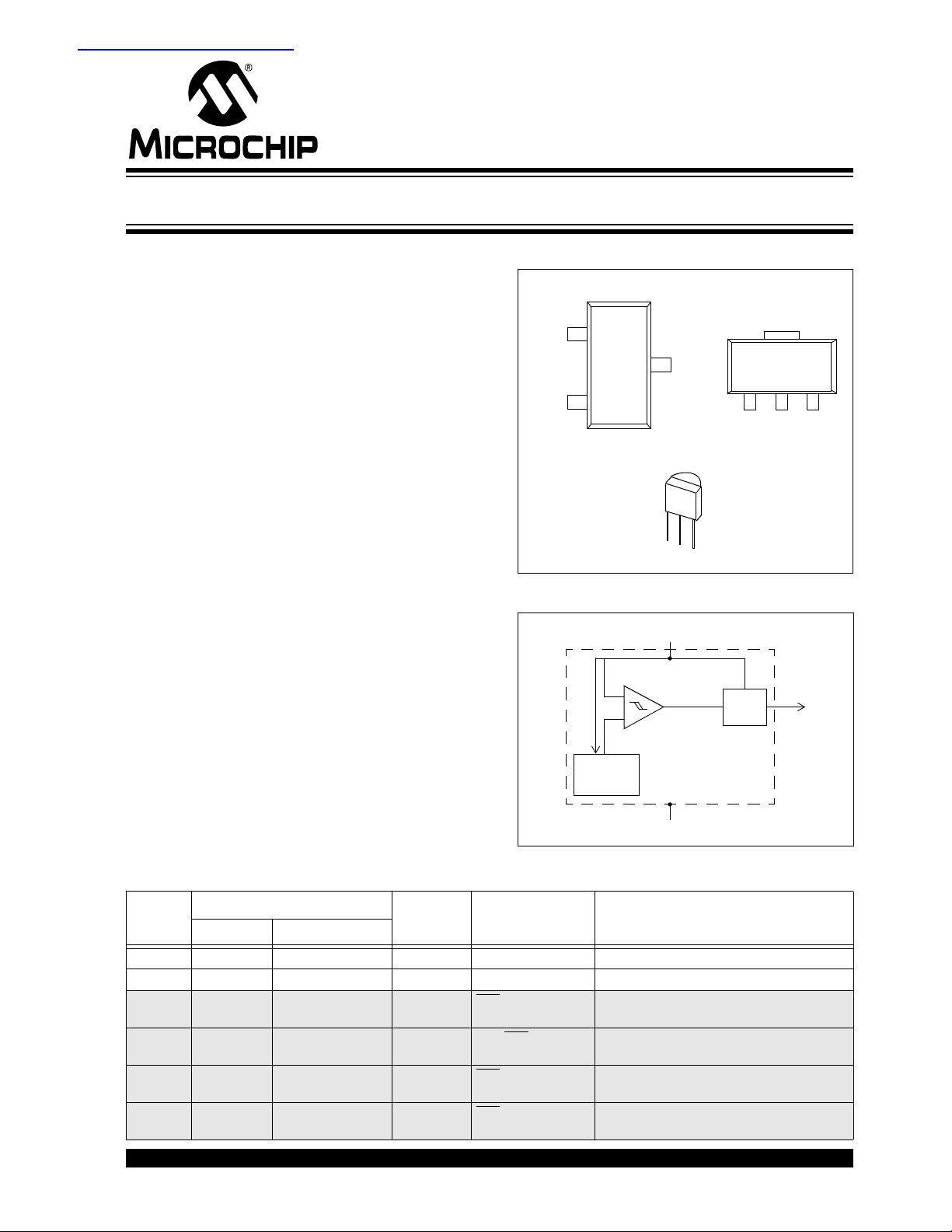
Package Types
3-Pin SOT23-3/SC-70
3-Pin SOT-89
• Precision monitoring options of:
V
- 1.90V, 2.32V, 2.63V, 2.90V, 2.93V, 3.08V,
4.38V and 4.63V
• Resets microcontroller in a power-loss event
•Active-low V
OUT
pin:
- MCP111 active-low, open-drain
- MCP112 active-low, push-pull
V
OUT
V
SS
1
V
3
DD
2
MCP111/112
DD
MCP111/112
1 32
V
V
OUT
• Available in SOT23-3, TO-92, SC-70 and
SOT-89-3 packages
3-Pin TO-92
• Temperature Range:
- Extended: -40°C to +125°C
(except MCP1XX-195)
- Industrial: -40°C to +85°C (MCP1XX-195 only)
• Pb-free devices
V
OUT
V
V
SS
DD
Applications
• Critical Microcontroller and Microprocessor
Power-Monitoring Applicati ons
• Computers
• Intelligent Instruments
• Portable Battery-Powered Equipm en t
Description
The MCP111/112 are voltage-detecting devices
designed to keep a microcontroller in reset until the
system voltage has stabilized at the appropriate level
for reliable system operation. These devices also
operate as protection from brown-out conditions when
the system supply voltage drops below the specified
threshold voltage level. Eight different trip voltag es a re
available.
TABLE 1: DEVICE FEATURES
Device
Output
Type Pull-up Resistor
MCP111 Open-drain External No V
MCP112 Push-pull No No V
MCP102 Push-pull No 120 ms RST, VDD, VSS See MCP102/103/121/131 Data Sheet
MCP103 Push-pull No 120 ms VSS, RST, VDD See MCP102/103/121/131 Data Sheet
MCP121 Open-drain External 120 ms RST, VDD, VSS See MCP102/103/121/131 Data Sheet
MCP131 Open-Drain Internal (~95 kΩ) 120 ms RST, VDD, VSS See MCP102/103/121/131 Data Sheet
Reset Delay
(typ)
Block Diagram
Package Pin Out
(Pin # 1, 2, 3)
, VSS, V
OUT
OUT
, VSS, V
DD
DD
Band Gap
Reference
(DS21906)
(DS21906)
(DS21906)
(DS21906)
V
Comparator
+
–
V
DD
SS
Output
Driver
Comment
V
DD
OUT
V
SS
© 2005 Microchip Technology Inc. DS21889D-page 1
Page 2

MCP111/112
1.0 ELECTRICAL
CHARACTERISTICS
† Notice: Stresses above those listed under “Maximum
Ratings” may cause permanent damage to the device. This is
a stress rating only and functional operation of the device at
those or any other conditions above those indicated in the
Absolute Maximum Ratings†
operational listings of this specification is not implied.
Exposure to maximum rating conditions fo r ext ended pe riods
VDD . . . . . . . . . . . . . . . . . . . . . . . . . . . . . . . . . . . . . . . . . 7.0V
Input current (V
Output current (RST
Rated Rise Time of V
All inputs and outputs (except RST
) . . . . . . . . . . . . . . . . . . . . . . . . . . . .10 mA
DD
) . . . . . . . . . . . . . . . . . . . . . . . . . .10 mA
. . . . . . . . . . . . . . . . . . . . . . 100V/µs
DD
) w.r.t. V
SS
may affect device reliability.
. . . . . . . . . . . . . . . . . . . . . . . . . . . . . . .-0 . 6 V to (VDD + 1.0V)
output w.r.t. VSS . . . . . . . . . . . . . . . . . . . -0.6 V to 1 3 .5 V
RST
Storage temperature. . . . . . . . . . . . . . . . . . .65°C to + 150°C
Ambient temp. with power applied . . . . . . . -40°C to + 125°C
Maximum Junction temp. with power applied . . . . . . . .150°C
ESD protection on all pins. . . . . . . . . . . . . . . . . . . . . . . . . ≥ 2kV
DC CHARACTERISTICS
Electrical Specifications: Unless otherwise indicated, all limits are specified for VDD = 1V to 5.5V, RPU = 100 kΩ (only MCP111),
T
= -40°C to +125°C.
A
Parameters Sym Min Typ Max Units Conditions
Operating Voltage Range V
Specified V
Value to V
DD
low V
OUT
Operating Current I
V
Trip Point MCP1XX-195 V
DD
DD
DD
DD
TRIP
MCP1XX-240 2.285 2.320 2.355 V T
MCP1XX-270 2.591 2.630 2.670 V T
MCP1XX-290 2.857 2.900 2.944 V T
MCP1XX-300 2.886 2.930 2.974 V T
MCP1XX-315 3.034 3.080 3.126 V T
MCP1XX-450 4.314 4.380 4.446 V T
MCP1XX-475 4.561 4.630 4.700 V T
Trip Point Tempco T
V
DD
TPCO
Note 1: Trip point is ±1.5% from typical value.
2: Trip point is ±2.5% from typical value.
3: This specification allows this device to be used in PICmicro
Serial Programming™ (ICSP™) feature (see device-specific programming specifications for voltage requirements).
This specification DOES NOT allow a continuous high voltage to be present on the open-drain output pin (V
total time that the V
V
pin should be limited to 2 mA. It is recommended that the device operational temperature be maintained between
OUT
pin can be above the maximum device operational voltage (5.5V) is 100 sec. Current into the
OUT
0°C to 70°C (+25°C preferred). For additional information, please refer to Figure 2-28.
4: This parameter is established by characterization and is not 100% tested.
1.0 — 5.5 V
1.0 — V I
= 10 µA, V
RST
RST
—< 11.75µA
1.872 1.900 1.929 V TA = +25°C (Note 1)
1.853 1.900 1.948 V T
= -40°C to +85°C (Note 2)
A
= +25°C (Note 1)
A
2.262 2.320 2.378 V Note 2
= +25°C (Note 1)
A
2.564 2.630 2.696 V Note 2
= +25°C (Note 1)
A
2.828 2.900 2.973 V Note 2
= +25°C (Note 1)
A
2.857 2.930 3.003 V Note 2
= +25°C (Note 1)
A
3.003 3.080 3.157 V Note 2
= +25°C (Note 1)
A
4.271 4.380 4.490 V Note 2
= +25°C (Note 1)
A
4.514 4.630 4.746 V Note 2
— ±100 — ppm/°
C
®
microcontroller applications that require the In-Circuit
< 0.2V
). The
OUT
DS21889D-page 2 © 2005 Microchip Technology Inc.
Page 3

MCP111/112
DC CHARACTERISTICS (CONTINUED)
Electrical Specifications: Unless otherwise indicated, all limits are specified for VDD = 1V to 5.5V, RPU = 100 kΩ (only MCP111),
= -40°C to +125°C.
T
A
Parameters Sym Min Typ Max Units Conditions
Threshold Hysteresis
(min. = 1%, max = 6%)
Low-level Output Voltage V
V
OUT
V
High-level Output Voltage V
OUT
Open-drain High Voltage on Output V
Open-drain Output Leakage Current
(MCP111 only)
Note 1: Trip point is ±1.5% from typical value.
2: Trip point is ±2.5% from typical value.
3: This specification allows this device to be used in PICmicro
Serial Programming™ (ICSP™) feature (see device-specific programming specifications for voltage requirements).
This specification DOES NOT allow a continuous high voltage to be present on the open-drain output pin (V
total time that the V
V
pin should be limited to 2 mA. It is recommended that the device operational temperature be maintained between
OUT
0°C to 70°C (+25°C preferred). For additional information, please refer to Figure 2-28.
4: This parameter is established by characterization and is not 100% tested.
MCP1XX-195 V
HYS
0.019 — 0.114 V TA = +25°C
MCP1XX-240 0.023 — 0.139 V
MCP1XX-270 0.026 — 0.158 V
MCP1XX-290 0.029 — 0.174 V
MCP1XX-300 0.029 — 0.176 V
MCP1XX-315 0.031 — 0.185 V
MCP1XX-450 0.044 — 0.263 V
MCP1XX-475 0.046 — 0.278 V
OL
OH
——0.4VI
VDD – 0.6 — — V IOH = 1 mA, For only MCP112
= 500 µA, V
OL
DD
(push-pull output)
— — 13.5
ODH
(3)
VMCP111 only,
= 3.0V, Time voltage >
V
DD
5.5V applied ≤ 100s,
current into pin limited to
2 mA , +25°C operation
recommended
Note 3, Note 4
I
OD
pin can be above the maximum device operational voltage (5.5V) is 100 sec. Current into the
OUT
—0.1—µA
®
microcontroller applications that require the In-Circuit
= V
OUT
TRIP(MIN)
). The
© 2005 Microchip Technology Inc. DS21889D-page 3
Page 4
MCP111/112
V
TRIP
1V
V
V
OUT
DD
1V
t
RPU
t
RPD
V
OH
V
OL
t
RT
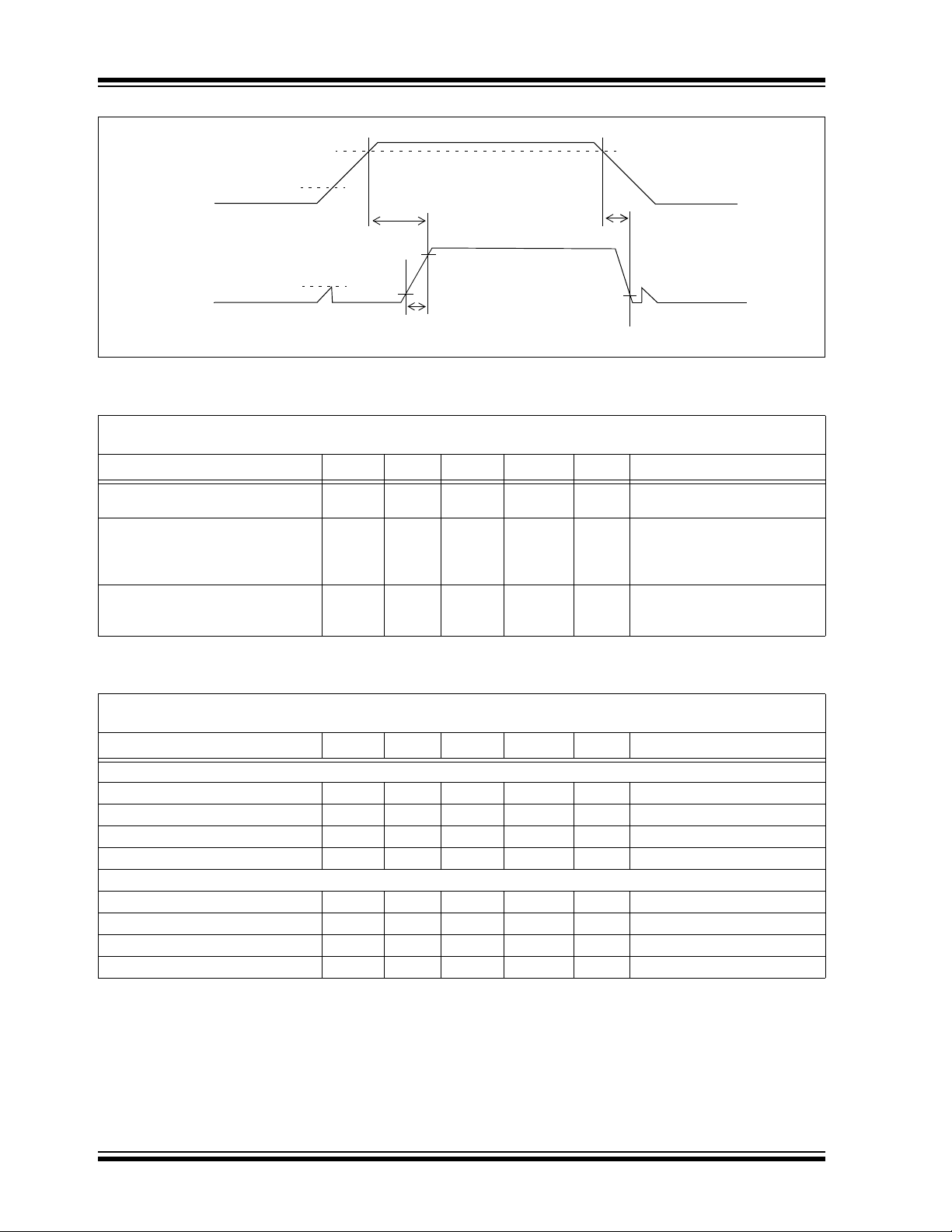
FIGURE 1-1: Timing Diagram.
AC CHARACTERISTICS
Electrical Specifications: Unless otherwise indicated, all limits are specified for VDD = 1V to 5.5V, RPU = 100 kΩ
(only MCP111), T
VDD Detect to V
Detect to V
V
DD
Rise Time After V
V
OUT
Note 1: These parameters are for design guidance only and are not 100% tested.
= -40°C to +125°C.
A
Parameters Sym Min Typ Max Units Conditions
Inactive t
OUT
Active
OUT
Active t
OUT
RPU
t
RPD
RT
—90 — µs
— 130 — µs
—5 —µs
Figure 1-1 and C
(Note 1)
V
ramped from V
DD
250 mV down to V
250 mV, per Figure 1-1,
C
= 50 pF (Note 1)
L
For V
value per Figure 1-1, C
(Note 1)
10% to 90% of final
OUT
= 50 pF
L
TRIP(MAX)
TRIP(MIN)
–
= 50 pF
L
+
TEMPERATURE CHARACTERISTICS
Electrical Specifications: Unless otherwise noted, all limits are specified for V
(only MCP111), T
Temperature Ranges
Specified Temperature Range T
Specified Temperature Range T
Maximum Junction Temperature T
Storage Temperature Range T
Package Thermal Resistances
Thermal Resistance, 3L-SOT23 θ
Thermal Resistance, 3L-SC-70 θ
Thermal Resistance, 3L-TO-92 θ
Thermal Resistance, 3L-SOT-89 θ
= -40°C to +125°C.
A
Parameters Sym Min Typ Max Units Conditions
A
A
J
A
JA
JA
JA
JA
-40 — +85 °C MCP1XX-195
-40 — +125 °C Except MCP1XX-195
——+150°C
-65 — +150 °C
— 336 — °C/W
— 340 — °C/W
—131.9 — °C/W
—110 —°C/W
= 1V to 5.5V, RPU = 100 kΩ
DD
DS21889D-page 4 © 2005 Microchip Technology Inc.
Page 5
MCP111/112
0
0
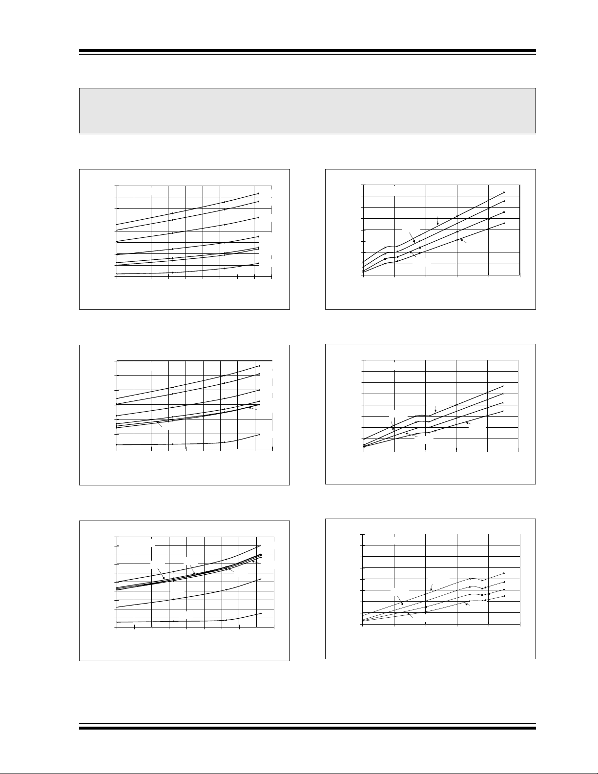
2.0 TYPICAL PERFORMANCE CURVES
Note: The graphs and tables provided fol lowi ng this note are a st a tis tic al s umm ary based on a lim ite d n um ber of
samples and are provided for informational purposes only. The performance characteristics listed herein
are not tested or guaranteed. In some graphs or tables, the data presented may be outside the specified
operating range (e.g., outside specified power supply range) and therefore outside the warranted range.
Note: Unless otherwise indicated, all limits are specified for VDD = 1V to 5.5V, RPU = 100 kΩ (only MCP111;
see Figure 4-1), T
= -40°C to +125°C.
A
1.6
MCP111-195
1.4
1.2
1
0.8
(uA)
DD
I
0.6
0.4
0.2
0
-40
-20
0
FIGURE 2-1: I
(MCP111-195).
1.2
MCP112-300
1
0.8
0.6
(uA)
DD
I
0.4
0.2
0
-40
-20
0
20
40
60
Temperature (°C)
vs. Temperature
DD
2.1V
20
40
60
Temperature (°C)
1.6
5.5V
5.0V
4.0V
2.8V
2.1V
1.7V
1.0V
80
100
120
140
FIGURE 2-4: I
5.5V
5.0V
4.0V
2.8V
1.7V
1.0V
80
100
120
140
MCP111-195
1.4
1.2
1
0.8
(uA)
DD
I
0.6
0.4
0.2
0
1.02.03.04.05.06.
1.6
MCP112-300
1.4
1.2
1
0.8
(uA)
DD
I
0.6
0.4
0.2
0
1.0 2.0 3.0 4.0 5.0 6.0
+85°C
+125°C
+85°C
-40°C
+25°C
V
(V)
DD
vs. VDD (MCP111-195).
DD
+125°C
-40°C
+25°C
V
(V)
DD
FIGURE 2-2: I
vs. Temperature
DD
FIGURE 2-5: I
vs. VDD (MCP112-300).
DD
(MCP112-300).
1
MCP112-475
0.9
0.8
0.7
0.6
0.5
(uA)
DD
0.4
I
0.3
0.2
0.1
0
-40
-20
5.0V
0
FIGURE 2-3: I
4.0V
1.7V
1.0V
20
40
60
Temperature (°C)
vs. Temperature
DD
5.5V
2.1V
2.8V
80
100
120
140
1.6
MCP112-475
1.4
1.2
1
0.8
(uA)
DD
I
0.6
0.4
0.2
0
1.0 2.0 3.0 4.0 5.0 6.
+85°C
FIGURE 2-6: I
+125°C
-40°C
+25°C
V
(V)
DD
vs. VDD (MCP112-475).
DD
(MCP112-475).
© 2005 Microchip Technology Inc. DS21889D-page 5
Page 6
MCP111/112
Note: Unless otherwise indicated, all limits are specified for VDD = 1V to 5.5V, RPU = 100 kΩ (only MCP111;
see Figure 4-1), T
1.950
1.945
1.940
1.935
1.930
(V)
1.925
1.920
TRIP
V
1.915
1.910
1.905
1.900
1.895
-60 -10 40 90 140
= -40°C to +125°C.
A
V
, Hysteresis
HYS
MCP111-195
max temp is
+85°C
V
, V decreasing
TRIP
Temperature (°C)
V
, V increasing
TRIP
0.050
0.045
0.040
0.035
0.030
0.025
0.020
0.015
0.010
0.005
0.000
0.120
MCP111-195
= 1.7V
V
0.100
0.080
(V)
0.060
OL
Hyst (V)
V
0.040
0.020
DD
+125°C
+85°C
-40°C
+25°C
0.000
0.00 0.25 0.50 0.75 1.00
I
(mA)
OL
FIGURE 2-7: V
TRIP
and V
Temperature (MCP111-195).
3.040
V
, V increasing
TRIP
MCP112-300
V
, V decreasing
TRIP
V
, Hysteresis
HYS
(V)
TRIP
V
3.020
3.000
2.980
2.960
2.940
2.920
2.900
-60 -10 40 90 140
Temperature (°C)
FIGURE 2-8: V
TRIP
and V
Temperature (MCP112-300).
4.800
4.780
4.760
4.740
4.720
(V)
4.700
4.680
TRIP
V
4.660
4.640
4.620
4.600
4.580
V
, V increasing
TRIP
MCP112-475
V
, V decreasing
TRIP
-60 -20 20 60 100 140
Temperature (°C)
V
, Hysteresis
HYS
HYST
HYST
vs.
0.100
0.098
0.096
0.094
0.092
0.090
0.088
0.086
0.084
0.082
vs.
0.180
0.170
0.160
0.150
0.140
0.130
0.120
0.110
0.100
FIGURE 2-10: V
(MCP111-195 @V
0.080
MCP112-300
0.070
V
DD
= 2.7V
OL
= 1.7V).
DD
vs. IOL
0.060
0.050
(V)
0.040
OL
V
Hyst (V)
0.030
0.020
0.010
+125°C
+85°C
-40°C
+25°C
0.000
0.00 0.25 0.50 0.75 1.00
I
(mA)
OL
FIGURE 2-11: V
(MCP112-300 @V
0.050
MCP112-475
= 4.4V
V
0.040
0.030
(V)
OL
V
Hyst (V)
0.020
0.010
DD
OL
= 2.7V).
DD
+85°C
vs. IOL
+125°C
-40°C
+25°C
0.000
0.00 0.25 0.50 0.75 1.00
(mA)
I
OL
FIGURE 2-9: V
TRIP
and V
Temperature (MCP112-475).
HYST
vs.
FIGURE 2-12: V
(MCP112-475 @V
DD
vs. IOL
OL
= 4.4V).
DS21889D-page 6 © 2005 Microchip Technology Inc.
Page 7
MCP111/112
0
Note: Unless otherwise indicated, all limits are specified for VDD = 1V to 5.5V, RPU = 100 kΩ (only MCP111;
see Figure 4-1), T
= -40°C to +125°C.
A
(V)
OL
V
0.120
0.100
0.080
0.060
0.040
0.020
0.000
MCP111-195
= 1.7 V
V
DD
-40 0 40 80 120
Temperature (°C)
IOL = 1.00 mA
IOL = 0.75 mA
IOL = 0.50 mA
IOL = 0.25 mA
IOL = 0.00 mA
FIGURE 2-13: VOL vs. Temperature
(MCP111-195 @ V
0.080
MCP112-300
(V)
OL
V
0.070
0.060
0.050
0.040
0.030
0.020
0.010
0.000
= 2.7V
V
DD
-40 0 40 80 120
= 1.7V).
DD
Temperature (°C)
IOL = 1.00 mA
I
= 0.75 mA
OL
IOL = 0.50 mA
IOL = 0.25 mA
IOL = 0.00 mA
(V)
OH
V
3.150
3.100
3.050
3.000
2.950
2.900
MCP112-300
= 3.1V
V
DD
0.00 0.25 0.50 0.75 1.0
FIGURE 2-16: V
(MCP112-300 @ V
4.820
4.800
4.780
4.760
(V)
OH
4.740
V
4.720
4.700
4.680
0.00 0.25 0.50 0.75 1.00
DD
IOL (mA)
vs. IOH
OH
= 3.1V).
(mA)
I
OL
-40 °C
+85 °C
+25 °C
+85 °C
+25 °C
+125 °C
MCP112-475
V
= 4.8V
DD
-40 °C
+125 °C
FIGURE 2-14: V
(MCP112-300 @ V
0.050
MCP112-475
V
0.040
0.030
(V)
OL
V
0.020
0.010
0.000
-40 0 40 80 120
DD
DD
= 4.4V
FIGURE 2-15: V
(MCP112-475 @ V
DD
vs. Temperature
OL
= 2.7V).
IOL = 1.00 mA
Temperature (°C)
vs. Temperature
OL
= 4.4V).
IOL = 0.75 mA
IOL = 0.50 mA
IOL = 0.25 mA
IOL = 0.00 mA
FIGURE 2-17: V
(MCP112-475 @ V
600
500
400
300
200
100
Transient Duration (µs)
MCP112-300
MCP112-475
0
0.001 0.01 0.1 1 10
OH
= 4.8V).
DD
MCP111-195
V
TRIP
vs. IOH
(min) - V
DD
FIGURE 2-18: Typical Transient Response
(25 °C).
© 2005 Microchip Technology Inc. DS21889D-page 7
Page 8
MCP111/112
Note: Unless otherwise indicated, all limits are specified for VDD = 1V to 5.5V, RPU = 100 kΩ (only MCP111;
see Figure 4-1), T
= -40°C to +125°C.
A
350
300
VDD decreasing from:
5V - 1.7V
250
200
(µs)
150
RPD
t
100
VDD decreasing from:
5V - 0V
50
0
-40 -15 10 35 60 85 110
FIGURE 2-19: t
(MCP111-195).
160
MCP112-300
140
120
100
VDD decreasing from:
(µs)
5V - 2.7V
80
RPD
t
60
40
VDD decreasing from:
20
5V - 0V
0
-40 -15 10 35 60 85 110
VDD decreasing from:
V
+ 0.25V to V
TRIP(max)
Temperature (°C)
vs. Temperature
RPD
VDD decreasing from:
V
+ 0.25V to V
TRIP(max)
Temperature (°C)
MCP111-195
- 0.25V
TRIP(min)
- 0.25V
TRIP(min)
400
350
300
250
(µs)
200
RPU
t
150
100
VDD increasing from:
0V - 2.8V
50
0
-40 -15 10 35 60 85 110
FIGURE 2-22: t
(MCP111-195).
140
120
100
80
(µs)
60
RPU
t
40
20
0
-40 -15 10 35 60 85 110
VDD increasing from:
0V - 2.1V
Temperature (°C)
vs. Temperature
RPU
VDD increasing from:
0V - 3.1V
VDD increasing from:
0V - 3.3V
VDD increasing from:
0V - 4.0V
VDD increasing from:
0V - 5.5V
Temperature (°C)
MCP111-195
VDD increasing
from: 0V - 4.0V
VDD increasing
from: 0V - 5.5V
MCP112-300
FIGURE 2-20: t
(MCP112-300).
250
VDD decreasing from:
5V - 4.4V
200
150
(µs)
VDD decreasing from:
RPD
t
100
50
0
+ 0.25V to V
V
TRIP(max)
VDD decreasing from:
5V - 0V
-40 -15 10 35 60 85 110
FIGURE 2-21: t
(MCP112-475).
vs. Temperature
RPD
- 0.25V
TRIP(min)
Temperature (°C)
vs. Temperature
RPD
MCP112-475
FIGURE 2-23: t
(MCP112-300).
250
200
150
(µs)
RPU
100
t
50
0
-40 -15 10 35 60 85 110
FIGURE 2-24: t
(MCP112-475).
vs. Temperature
RPU
VDD increasing from:
0V - 4.9V
VDD increasing from:
0V - 5.0V
VDD increasing from:
0V - 5.5V
Temperature (°C)
vs. Temperature
RPU
MCP112-475
DS21889D-page 8 © 2005 Microchip Technology Inc.
Page 9

MCP111/112
Note: Unless otherwise indicated, all limits are specified for VDD = 1V to 5.5V, RPU = 100 kΩ (only MCP111;
see Figure 4-1), T
= -40°C to +125°C.
A
60
55
50
45
40
(µs)
RT
t
35
30
25
20
-40 -15 10 35 60 85 110
VDD increasing from:
0V - 2.1V
VDD increasing from:
0V - 5.5V
Temperature (°C)
MCP111-195
VDD increasing
from: 0V - 4.0V
VDD increasing from:
0V - 2.8V
FIGURE 2-25: tRT vs. Temperature
(MCP111-195).
0.4
0.35
VDD increasing from:
0V - 3.3V
0.3
0.25
0.2
(µs)
RT
t
0.15
VDD increasing from:
0.1
0V - 4.0V
0.05
0
-40 -15 10 35 60 85 110
VDD increasing from:
0V - 3.1V
MCP112-300
Temperature (°C)
VDD increasing from:
0V - 5.5V
0.1500
0.1400
0.1300
VDD increasing from:
0V - 4.9V
0.1200
(µs)
RT
t
0.1100
0.1000
0.0900
0.0800
VDD increasing from:
0V - 4.8V
-40 -15 10 35 60 85 110
FIGURE 2-27: t
(MCP112-475).
1.E-02
10m
1.E-03
1m
1.E-04
100µ
1.E-05
10µ
1.E-06
1µ
1.E-07
100n
1.E-08
10n
1.E-09
1n
1.E-10
100p
1.E-11
10p
Open-Drain Leakage (A)
1.E-12
1p
1.E-13
100f
0 1 2 3 4 5 6 7 8 9 10 11 12 13 14
VDD increasing from:
0V - 5.0V
VDD increasing from:
0V - 5.5V
Temperature (°C)
vs. Temperature
RT
125°C
25°C
Pull-Up Voltage (V)
MCP112-475
- 40°C
FIGURE 2-26: t
(MCP112-300).
vs. Temperature
RT
FIGURE 2-28: Open-Drain Leakage
Current vs. Voltage Applied to V
OUT
Pin
(MCP111-195).
© 2005 Microchip Technology Inc. DS21889D-page 9
Page 10

MCP111/112
3.0 PIN DESCRIPTION
The descriptions of the pins are listed in Table 3-1.
TABLE 3-1: PIN FUNCTION TABLE
Pin No.
SOT-23-3
SC-70
SOT-89-3 T0-92
111V
223VSSGround reference
332V
—4—VDDPositive power supply
Symbol Function
OUT
Output State
Falling:
V
DD
H = V
DD
> V
L = VDD < V
VDD Rising:
DD
> V
H = V
L = VDD < V
Positive power supply
DD
TRIP
TRIP
TRIP
TRIP
+ V
+ V
HYS
HYS
DS21889D-page 10 © 2005 Microchip Technology Inc.
Page 11

MCP111/112
r
4.0 APPLICATION INFORMATION
For many of today’s microcontroller applicat ions, care
must be taken to prevent low-power conditions that can
cause many different system problems. The most
common causes are brown-out condition s, where the
system supply drops below the operating level momentarily. The second most common cause is when a slowly
decaying power supply causes the microcontroller to
begin executing instructions without sufficient voltage to
sustain SRAM, thus producing indeterminate results.
Figure 4-1 shows a typical application circuit.
V
DD
3
V
0.1
µF
DD
MCP11X
V
V
SS
OUT
R
PU
(1)
1
2
Note 1: RPU may be required with the MCP111
due to the open-drain output. Resisto
RPU is not required with the MCP112.
V
DD
PICmicro
®
Microcontroller
MCLR
(Reset Input)
GND
4.1 V
The voltage trip point (V
edge of V
be between the minimum trip point (V
maximum trip point (V
Operation
TRIP
) is determined on the falling
. The actu al vol tage tr ip point (V
DD
TRIP
). There is a hysteresis on
TRIPMAX
TRIPMIN
) will
TRIPAC
) and the
this trip point to remove any “jitter” that would occur on
the V
Figure 4-2 shows the state of the V
determined by the V
is for falling V
rising, the V
V
pin when the device VDD is at the trip point.
OUT
voltage. The V
DD
voltages. When the VDD voltage is
DD
pin will not be drive n h igh unt il VDD is at
OUT
+ V
HYS
.
TRIP
pin as
OUT
specification
TRIP
FIGURE 4-1: Typical Application Circuit.
VDD
V
TRIPMAX
V
TRIPMIN
1V
V
OUT
FIGURE 4-2: V
Operation as Determined by the V
OUT
< 1 V is outside the
device speci fications
V
TRIPAC
+ V
HYSAC
TRIP
V
and V
TRIPAC
HYS
V
TRIPAC
.
© 2005 Microchip Technology Inc. DS21889D-page 11
Page 12

MCP111/112
4.2 Negative Going VDD Transients
The minimum pulse width (time) required to cause a
reset may be an important criteria in the implementation of a Power-on Reset (POR) circuit. This time is
referred to as transient dur ation, defined as the amount
of time needed for these supervisory devices to
respond to a drop in V
dependant on the magnitu de of V
speaking, the transient duration decreases with
increases in V
TRIP
Figure 4-3 shows a typ ical tran sient dur ation vs . reset
comparator overdrive for which the MCP111/112 will
not generate a reset pulse. It shows that the farther
below the trip point the transient pulse goes, the
duration of the pulse required to cause a reset gets
shorter. Figure 2-18 shows the transient response
characteristics for the MCP111/112.
A 0.1 µF bypass capacitor, mounted as close as
possible to the V
immunity (refer to Figure4-1).
5V
Supply Voltage
0V
FIGURE 4-3: Example of Typical
Transient Duration Waveform.
. The transient du ration tim e is
DD
– VDD. Generally
TRIP
– VDD.
pin, provides additional transient
DD
V
TRIP(MAX)
V
TRIP(MIN)
t
TRANS
Time (µs)
V
TRIP(MIN)
- V
DD
4.3 Effect of Temperature on Time-ou t
Period (t
The time-out period (t
device remains in the reset condition. This is affected
by both VDD and temperature. The graph shown in
Figures 2-22, 2-23 and 2-24 show the typical respo nse
for different VDD values and temperatures.
)
RPU
) determines how long the
RPU
4.4 Using in PICmicro®
Microcontroller ICSP™
Applications (MCP111 only)
Figure 4-4 shows the typical application circuit for using
the MCP111 for voltage supervisory function when the
PICmicro mi crocontroller will be programmed via the
In-Circuit Serial Programming™ (ICSP)
feature. Additional information is available in TB087,
“Using Voltage Supervisors with PICmicro
troller Systems which Implement In-Circuit Serial
Programming™”, DS91087.
Note: It is recommend ed that th e current into the
pin be current limited by a 1kΩ
RST
resistor.
VDD/V
0.1 µF
R
V
DD
PU
MCP111
RST
V
SS
1kΩ
®
Microcon-
PP
V
DD
PICmicro
MCU
MCLR
(reset input)
(Active-Low)
V
SS
®
FIGURE 4-4: Typical Application Circuit
for PICmicro
®
Microcontroller with the ICSP™
feature.
DS21889D-page 12 © 2005 Microchip Technology Inc.
Page 13
5.0 PACKAGING INFORMATION
5.1 Package Marking Information
MCP111/112
3-Pin SOT-23
XXNN
3-Lead TO-92
XXXXXX
XXXXXX
XXXXXX
YWWNNN
Example:
MCP111
290E
TO^^
3
e
547256
Example:
Part Number SOT-23 Part Number SOT-23
MCP111T-195I/TT MPNN MCP112T-195I/TT MRNN
MCP111T-240ETT MQNN MCP112T-240ETT MSNN
MCP111T-270E/TT MGNN MCP112T-270E/TT MANN
MCP111T-290E/TT NHNN MCP112T-290E/TT MBNN
MCP111T-300E/TT MJNN MCP112T-300E/TT MCNN
MCP111T-315E/TT MKNN MCP112T-315E/TT MDNN
MCP111T-450E/TT MLNN MCP112T-450E/TT MENN
MCP111T-475E/TT MMNN MCP112T-475E/TT MFNN
3-Pin SOT-89
Part Number SOT-89 Part Number SOT-89
XXYYWW
NNN
Legend: XX...X Customer-specific information
Y Year code (last digit of calendar year)
WW Week code (week of January 1 is week ‘01’)
NNN Alphanumeric traceability code
3
e
Pb-free JEDEC designator for Matte Tin (Sn)
* This package is Pb-free. T he Pb-free JEDEC designator ( )
can be found on the outer packaging for this package.
Note: In the event the full Microchip part nu mber ca nnot be m arked o n one lin e, it will
be carried over to the next line, thus limiting the number of available
characters for customer-specific information.
MCP111T-195I/MB MP MCP112T-195I/MB MR
MCP111 T-240EMB MQ MCP112T-240EMB MS
MCP111T-270E/MB MG MCP112T-270E/MB MA
MCP111T-290E/MB NH MCP112T-290E/MB MB
MCP111T-300E/MB MJ MCP112T-300E/MB MC
MCP111T-315E/MB MK MCP112T-315E/MB MD
MCP111T-450E/MB ML MCP112T-450E/MB ME
MCP111T-475E/MB MM MCP112T-475E/MB MF
Example:
3
e
© 2005 Microchip Technology Inc. DS21889D-page 13
Page 14

MCP111/112
Package Marking Information (Continued)
3-Pin SC-70
XXN
Top Side
OR
XXNN
Top Side
Example:
Part Number SC-70 Part Number SC-70
MCP111T-195I/LB EPN MCP112T-195I/LB ERN
MCP111T-240E/LB EQN MCP112T-240E/LB ESN
MCP111T-270E/LB EGN MCP112T-270E/LB EAN
MCP111T-290E/LB EHN MCP112T-290E/LB EBN
MCP111T-300E/LB EJN MCP112T-300E/LB ECN
MCP111T-315E/LB EKN MCP112T-315E/LB EDN
MCP111T-450E/LB ELN MCP112T-450E/LB EEN
MCP111T-475E/LB EMN MCP112T-475E/LB EFN
Example:
Part Number SC-70 Part Number SC-70
MCP111T-195I/LB EPNN MCP112T-195I/LB ERNN
MCP111T-240E/LB EQNN MCP112T-240E/LB ESNN
MCP111T-270E/LB EGNN MCP112T-270E/LB EANN
MCP111T-290E/LB EHNN MCP112T-290E/LB EBNN
MCP111T-300E/LB EJNN MCP112T-300E/LB ECNN
MCP111T-315E/LB EKNN MCP112T-315E/LB EDNN
MCP111T-450E/LB ELNN MCP112T-450E/LB EENN
MCP111T-475E/LB EMNN MCP112T-475E/LB EFNN
DS21889D-page 14 © 2005 Microchip Technology Inc.
Page 15

3-Lead Plastic Small Outline Transistor (MB) (SOT89)
H
E
B1
3
B
MCP111/112
D1
D
2
R
1
B1
L
E1
A
C
Pitch
Outside lead pitch (basic)
Molded Package Width at Base
Molded Package Width at Top
Tab Corner Radii R 0.254.010
Foot Length L .035 .047 0.89 1.20
Lead Thickness
Leads 1 & 3 Width B1 .014 .019 0.36 0.48
*Controlling Parameter
Notes:
Dimensions D and E1 do not include mold or flash protrusions. Mold flash or protrusions
shall not exceed .005" (0.127mm) per side.
JEDEC Equivalent: TO-243
Drawing No. C04-29
p1
p
MILLIMETERS*INCHESUnits
p
p1
E .090 .102 2.29 2.60
c
Revised 07-24-03
MAXMINMAXMINDimension Limits
1.50 BSC.059 BSC
3.00 BSC.118 BSC
1.601.40.063.055AOverall Height
4.253.94.167.155HOverall Width
2.292.13.090.084E1
4.604.40.181.173DOverall Length
1.831.62.072.064D1Tab Length
0.440.35.017.014
0.560.43.022.017BLead 2 Width
© 2005 Microchip Technology Inc. DS21889D-page 15
Page 16

MCP111/112
3-Lead Plastic Small Outline Transistor (TT) (SOT-23)
E
E1
2
B
n
1
c
β
Number of Pins
Pitch
Outside lead pitch (basic)
Foot Angle
Lead Thickness
Mold Draft Angle Top
Mold Draft Angle Bottom
* Controlling Parameter
§ Significant Characteristic
Notes:
Dimensions D and E1 do not include mold flash or protrusions. Mold flash or protrusions shall not exceed
.010” (0.254mm) per side.
JEDEC Equivalent: TO-236
Drawing No. C04-104
n
p
p1
φ
c
α
β
p1
D
p
A
.038
A1
MILLIMETERSINCHES*Units
0.96
1.92.076
φ
L
α
A2
MAXNOMMINMAXNOMMINDimension Limits
33
1.121.010.89.044.040.035AOverall Height
1.020.950.88.040.037.035A2Molded Package Thickness
0.100.060.01.004.002.000A1Standoff §
2.642.372.10.104.093.083EOverall Width
1.401.301.20.055.051.047E1Molded Package Width
3.042.922.80.120.115.110DOverall Length
0.550.450.35.022.018.014LFoot Length
10501050
0.180.140.09.007.006.004
0.510.440.37.020.017.015BLead Width
10501050
10501050
DS21889D-page 16 © 2005 Microchip Technology Inc.
Page 17

3-Lead Plastic Small Outline Transistor (LB) (SC-70)
E
E1
MCP111/112
B
3
2
p1 D
p
1
a
c
b
Pitch
Outside lead pitch (basic)
Lead Thickness
Mold Draft Angle Top
Mold Draft Angle Bottom
*Controlling Parameter
Notes:
Dimensions D and E1 do not include mold flash or protrusions. Mold flash or protrusions
shall not exceed .005" (0.127mm) per side.
L
p
p1
c
a
b
A
.026 BSC.
.051 BSC.
A2
A1
MILLIMETERS*INCHESUnits
MAXMINMAXMINDimension Limits
33Number of Pins
0.65 BSC.
1.30 BSC.
1.100.80.043.031AOverall Height
1.000.80.039.031A2Molded Package Thickness
.0100.00.0004.000A1Standoff
2.401.80.094.071EOverall Width
1.351.15.053.045E1Molded Package Width
2.251.80.089.071DOverall Length
0.410.10.016.004LFoot Length
0.250.08.010.003
0.400.15.016.006BLead Width
12°8°12°8°
12°8°12°8°
JEITA (EIAJ) Equivalent: SC70
Drawing No. C04-104
© 2005 Microchip Technology Inc. DS21889D-page 17
Page 18
MCP111/112
3-Lead Plastic Transistor Outline (TO) (TO-92)
E1
D
1
Number of Pins
Pitch
Tip to Seating Plane L .500 .555 .610 12.70 14.10 15.49
Lead Thickness
Mold Draft Angle Top
Mold Draft Angle Bottom
*Controlling Parameter
Notes:
Dimensions D and E1 do not include mold flash or protrusions. Mold flash or protrusions shall not exceed
.010” (0.254mm) per side.
JEDEC Equivalent: TO-92
Drawing No. C04-101
n
L
1
2
3
B
p
c
R
n
p
c
α
β
β
MILLIMETERSINCHES*Units
α
A
MAXNOMMINMAXNOMMINDimension Limits
33
1.27.050
3.943.623.30.155.143.130ABottom to Package Flat
4.954.714.45.195.186.175E1Overall Width
4.954.644.32.195.183.170DOverall Length
2.412.292.16.095.090.085RMolded Package Radius
0.510.430.36.020.017.014
0.560.480.41.022.019.016BLead Width
654654
432432
DS21889D-page 18 © 2005 Microchip Technology Inc.
Page 19

MCP111/112
5.2 Product Tape and Reel Specifications
FIGURE 5-1: EMBOSSED CARRIER DIMENSIONS (8, 12, 16 AND 24 MM TAPE ONLY)
Top
Cover
Tape
A
0
W
K
0
B
0
P
TABLE 1: CARRIER TAPE/CAVITY DIMENSIONS
Carrier
Case
Outline
Package
Type
Dimensions
W
mm
P
mmA0mmB0mm
TT SOT-23B 3L 8 4 3.15 2.77 1.22 3000 180
LB SC-70 3L 8 4 2.4 2.4 1.19 3000 180
Cavity
Dimensions
K0
mm
Output
Quantity
Units
FIGURE 5-2: 3-LEAD SOT-23/SC70 DEVICE TAPE AND REEL SPECIFICATIONS
User Direction of Feed
Device
Marking
W
PIN 1
Standard Reel Component Orientation
P
Reel
Diameter in
mm
© 2005 Microchip Technology Inc. DS21889D-page 19
Page 20

MCP111/112
Pin 1
P, Pitch
W, Width
of Carrier
Tape
Pin 1
FIGURE 5-3: TO-92 DEVICES
Device
Marking
Seal
Tape
Back
Tape
Note: Bent leads are for Tape and Reel only.
MARK
FACE
MARK
FACE
MARK
FACE
User Direction of Feed
P
W
FIGURE 5-4: SOT-89 DEVICES
Standard Reel Component Orientation
User Direction of Feed
Reverse Reel Component Orientation
DS21889D-page 20 © 2005 Microchip Technology Inc.
Page 21

APPENDIX A: REVISION HISTORY
Revision D (June 2005)
1. Added SOT-89-3 package information
throughout.
Revision C (March 2005)
The following is the list of modifications:
1. Added Section 4.4 “Using in PICmicro®
Microcontroller ICSP™ Applications
(MCP111 only)” on using the MCP111 in
PICmicro microcontroller ICSP applications.
2. Added V
“Electrical Characteristics” (for ICSP
applications).
3. Added Figure 2-28.
4. Added devices features table to page 1.
5. Updated SC-70 package markings and added
Pb-free marking information to Section 5.0
“Packaging information”.
6. Added Appendix A: “Revision History”.
specifications in Section 1.0
ODH
MCP111/112
Revision B (August 2004)
1. Corrected package marking information in
Section 5 .0 “Packaging information”
Revision A (May 2004)
• Original Release of this Document.
© 2005 Microchip Technology Inc. DS21889D-page 21
Page 22

MCP111/112
NOTES:
DS21889D-page 22 © 2005 Microchip Technology Inc.
Page 23

MCP111/112
PRODUCT IDENTIFICATION SYSTEM
To order or obtain information, e.g., on pricing or delivery, refer to the factory or the listed sales office.
PART NO. XXX X
Device
Device: MCP111: MicroPo w er Voltage Detector, open-drain
Monitoring Options: 195 = 1.90V
Temperature Range: I = -40°C to +85°C (MCP11X-195 only)
Package: LB = SC-70, 3-lead
X
Tape/Reel
Option
Monitoring
Options
MCP111T: MicroPo w er Voltage Detector, open-drain
MCP112: MicroPower Voltage Detector, push-pull
MCP112T: MicroPo wer Voltage Detector, push-pull
240 = 2.32V
270 = 2.63V
290 = 2.90V
300 = 2.93V
315 = 3.08V
450 = 4.38V
475 = 4.63V
E = -40°C to +125°C (Except MCP11X-195 only)
MB = SOT-89, 3-lead
TO = TO-92, 3-lead
TT = SOT-23B, 3-lead
Temperature
Range
(Tape and Reel)
(Tape and Reel)
X
X
Package
Examples:
a) MC P111T-195I/TT: Tape and Reel,
b) MC P111T-315E/LB: Tape and Reel,
c) MCP111-300E/TO: 3.00V option, open-drain,
d) MCP111-315E/MB: 3.15V option, open-drain,
a) MC P112T-290E/TT: Tape and Reel,
b) MC P112T-475E/LB: Tape and Reel,
c) MCP112-450E/TO: 4.5V option, push-pull,
d) MCP112-315E/MB: 3.15V option, push-pull,
1.95V option, open-drain,
-40°C to +85°C,
SOT-23B package.
3.15V option, open-drain,
-40°C to +125°C,
SC-70-3 package.
-40°C to +125°C,
TO-92-3 package.
-40°C to +125°C,
SOT-89-3 package.
2.90V option, push-pull, 40°C to +125°C,
SOT-23B-3 package.
4.75V option, push-pull,
-40°C to +125°C,
SC-70-3 package.
-40°C to +125°C,
TO-92-3 package.
-40°C to +125°C,
SOT-89-3 package.
© 2005 Microchip Technology Inc. DS21889D-page 23
Page 24

MCP111/112
NOTES:
DS21889D-page 24 © 2005 Microchip Technology Inc.
Page 25

Note the following details of the code protection feature on Microchip devices:
• Microchip products meet the specification contained in their particular Microchip Data Sheet.
• Microchip believes that its family of products is one of the most secure families of its kind on the market today, when used in the
intended manner and under normal conditions.
• There are dishonest and possibly illegal methods used to breach the code protection feature. All of these methods, to our
knowledge, require using the Microchip products in a manner outside the operating specifications contained in Microchip’s Data
Sheets. Most likely, the person doing so is engaged in theft of intellectual property.
• Microchip is willing to work with the customer who is concerned about the integrity of their code.
• Neither Microchip nor any other semiconductor manufacturer can guarantee the security of their code. Code protection does not
mean that we are guaranteeing the product as “unbreakable.”
Code protection is constantly evolving. We at Microchip are com mitted to continuously improving the code protect ion f eatures of our
products. Attempts to break Microchip’s code protection feature may be a violation of the Digit al Mill ennium Copyright Act. If such acts
allow unauthorized access to your software or other copyrighted work, you may have a right to sue for relief under that Act.
Information contained in this publication regarding device
applications and the like is provided only for your convenience
and may be superseded by updates. It is your responsibility to
ensure that your application meets with your specifications.
MICROCHIP MAKES NO REPRESENTATIONS OR WARRANTIES OF ANY KIND WHETHER EXPRESS OR IMPLIED,
WRITTEN OR ORAL, STATUTORY OR OTHERWISE,
RELATED TO THE INFORMATION, INCLUDING BUT NOT
LIMITED TO ITS CONDITION, QUALITY, PERFORMANCE,
MERCHANTABILITY OR FITNESS FOR PURPOSE.
Microchip disclaims all liability arising from this information and
its use. Use of M icrochip’s prod ucts as critical components in
life support systems is not authorized except with express
written approval by Microchip. No licenses are conveyed,
implicitly or otherwise, under any Microchip intellectual property
rights.
Trademarks
The Microchip name and logo, the Microchip logo, Accuron,
dsPIC, K
EELOQ, microID, MPLAB, PIC, PICmicro,
PICSTART, PRO MATE, PowerSmart, rfPIC, a nd
SmartShunt are registered trademarks of Microchip
Technology Incorporated in the U.S.A. and other countries.
AmpLab, FilterLab, Migratable Memory, MXDEV, MXLAB,
PICMASTER, SEEVAL, SmartSensor and The Embedded
Control Solutions Company are registered trademarks of
Microchip Technology Incorporated in the U.S.A.
Analog-for-the-Digital Age, Application Maestro, dsPICDEM,
dsPICDEM.net, dsPICworks, ECAN, ECONOMONITOR,
FanSense, FlexROM, fuzzyLAB, In-Circuit Serial
Programming, ICSP, ICEPIC, Linear Active Thermistor,
MPASM, MPLIB, MPLINK, MPSI M, PICkit, PICDEM,
PICDEM.net, PICLAB, PICtail, PowerCal, PowerInfo,
PowerMate, PowerTool, rfLAB, rfPICDEM, Select Mode,
Smart Serial, SmartTel, Total Endurance and WiperLock are
trademarks of Microchip Technology Incorporated in the
U.S.A. and other countries.
SQTP is a service mark of Microchip T echnology Incorporated
in the U.S.A.
All other trademarks mentioned herein are property of their
respective companies.
© 2005, Microchip Technology Incorporated, Printed in the
U.S.A., All Rights Reserved.
Printed on recycled paper.
Microchip received ISO/TS-16949:2002 quality system certification for
its worldwide headquarters, design and wafer fabrication facilities in
Chandler and Tempe, Arizona and Mountain View, California in
October 2003. The Company’s quality system processes and
procedures are for its PICmicro
devices, Serial EEPROMs, microperipherals, nonvolatile memory and
analog products. In addition, Microchip’s quality system for the design
and manufacture of development systems is ISO 9001:2000 certified.
®
8-bit MCUs, KEELOQ
®
code hopping
© 2005 Microchip Technology Inc. DS21889D-page 25
Page 26

WORLDWIDE SALES AND SERVICE
AMERICAS
Corporate Office
2355 West Chandler Blvd.
Chandler, AZ 85224-6199
Tel: 480-792-7200
Fax: 480-792-7277
Technical Support:
http://support.microchip.com
Web Address:
www.microchip.com
Atlanta
Alpharetta, GA
Tel: 770-640-0034
Fax: 770-640-0307
Boston
Westborough, MA
Tel: 774-760-0087
Fax: 774-760-0088
Chicago
Itasca, IL
Tel: 630-285-0071
Fax: 630-285-0075
Dallas
Addison, TX
Tel: 972-818-7423
Fax: 972-818-2924
Detroit
Farmington Hills, MI
Tel: 248-538-2250
Fax: 248-538-2260
Kokomo
Kokomo, IN
Tel: 765-864-8360
Fax: 765-864-8387
Los Angeles
Mission Viejo, CA
Tel: 949-462-9523
Fax: 949-462-9608
San Jose
Mountain View, CA
Tel: 650-215-1444
Fax: 650-961-0286
Toronto
Mississauga, Ontario,
Canada
Tel: 905-673-0699
Fax: 905-673-6509
ASIA/PACIFIC
Australia - Sydney
Tel: 61-2-9868-6733
Fax: 61-2-9868-6755
China - Beijing
Tel: 86-10-8528-2100
Fax: 86-10-8528-2104
China - Chengdu
Tel: 86-28-8676-6200
Fax: 86-28-8676-6599
China - Fuzhou
Tel: 86-591-8750-3506
Fax: 86-591-8750-3521
China - Hong Kong SAR
Tel: 852-2401-1200
Fax: 852-2401-3431
China - Shanghai
Tel: 86-21-5407-5533
Fax: 86-21-5407-5066
China - Shenyang
Tel: 86-24-2334-2829
Fax: 86-24-2334-2393
China - Shenzhen
Tel: 86-755-8203-2660
Fax: 86-755-8203-1760
China - Shunde
Tel: 86-757-2839-5507
Fax: 86-757-2839-5571
China - Qingdao
Tel: 86-532-502-7355
Fax: 86-532-502-7205
ASIA/PACIFIC
India - Bangalore
Tel: 91-80-2229-0061
Fax: 91-80-2229-0062
India - New Delhi
Tel: 91-1 1-5160-8631
Fax: 91-11-5160-8632
Japan - Kanagawa
Tel: 81-45-471- 6166
Fax: 81-45-471-6122
Korea - Seoul
Tel: 82-2-554-7200
Fax: 82-2-558-5932 or
82-2-558-5934
Malaysia - Penang
Tel:011-604-646-8870
Fax:011-604-646-5086
Philippines - Manila
Tel: 01 1-632-634-9065
Fax: 011-632-634-9069
Singapore
Tel: 65-6334-8870
Fax: 65-6334-8850
Taiwan - Kaohsiung
Tel: 886-7-536-4818
Fax: 886-7-536-4803
Taiwan - Taipei
Tel: 886-2-2500-6610
Fax: 886-2-2508-0102
Taiwan - Hsinchu
Tel: 886-3-572-9526
Fax: 886-3-572-6459
EUROPE
Austria - Weis
Tel: 43-7242-2244-399
Fax: 43-7242-2244-393
Denmark - Ballerup
Tel: 45-4450-2828
Fax: 45-4485-2829
France - Massy
Tel: 33-1-69-53-63-20
Fax: 33-1-69-30-90-79
Germany - Ismaning
Tel: 49-89-627-144-0
Fax: 49-89-627-144-44
Italy - Milan
Tel: 39-0331-742611
Fax: 39-0331-466781
Netherlands - Drunen
Tel: 31-416-690399
Fax: 31-416-690340
England - Berkshire
Tel: 44-118-921-5869
Fax: 44-118-921-5820
04/20/05
DS21889D-page 26 © 2005 Microchip Technology Inc.
 Loading...