

Page 1

MCP1012
1W Demonstration Board
User’s Guide
2020 Microchip Technology Inc. DS50002932A
Page 2

Note the following details of the code protection feature on Microchip devices:
• Microchip products meet the specification contained in their particular Microchip Data Sheet.
• Microchip believes that its family of products is one of the most secure families of its kind on the market today, when used in the
intended manner and under normal conditions.
• There are dishonest and possibly illegal methods used to breach the code protection feature. All of these methods, to our
knowledge, require using the Microchip products in a manner outside the operating specifications contained in Microchip’s Data
Sheets. Most likely, the person doing so is engaged in theft of intellectual property.
• Microchip is willing to work with the customer who is concerned about the integrity of their code.
• Neither Microchip nor any other semiconductor manufacturer can guarantee the security of their code. Code protection does not
mean that we are guaranteeing the product as “unbreakable.”
Code protection is constantly evolving. We at Microchip are committed to continuously improving the code protection features of our
products. Attempts to break Microchip’s code protection feature may be a violation of the Digital Millennium Copyright Act. If such acts
allow unauthorized access to your software or other copyrighted work, you may have a right to sue for relief under that Act.
Information contained in this publication regarding device
applications and the like is provided only for your convenience
and may be superseded by updates. It is your responsibility to
ensure that your application meets with your specifications.
MICROCHIP MAKES NO REPRESENTATIONS OR
WARRANTIES OF ANY KIND WHETHER EXPRESS OR
IMPLIED, WRITTEN OR ORAL, STATUTORY OR
OTHERWISE, RELATED TO THE INFORMATION,
INCLUDING BUT NOT LIMITED TO ITS CONDITION,
QUALITY, PERFORMANCE, MERCHANTABILITY OR
FITNESS FOR PURPOSE. Microchip disclaims all liability
arising from this information and its use. Use of Microchip
devices in life support and/or safety applications is entirely at
the buyer’s risk, and the buyer agrees to defend, indemnify and
hold harmless Microchip from any and all damages, claims,
suits, or expenses resulting from such use. No licenses are
conveyed, implicitly or otherwise, under any Microchip
intellectual property rights unless otherwise stated.
Trademarks
The Microchip name and logo, the Microchip logo, Adaptec,
AnyRate, AVR, AVR logo, AVR Freaks, BesTime, BitCloud, chipKIT,
chipKIT logo, CryptoMemory, CryptoRF, dsPIC, FlashFlex,
flexPWR, HELDO, IGLOO, JukeBlox, KeeLoq, Kleer, LANCheck,
LinkMD, maXStylus, maXTouch, MediaLB, megaAVR, Microsemi,
Microsemi logo, MOST, MOST logo, MPLAB, OptoLyzer,
PackeTime, PIC, picoPower, PICSTART, PIC32 logo, PolarFire,
Prochip Designer, QTouch, SAM-BA, SenGenuity, SpyNIC, SST,
SST Logo, SuperFlash, Symmetricom, SyncServer, Tachyon,
TempTrackr, TimeSource, tinyAVR, UNI/O, Vectron, and XMEGA
are registered trademarks of Microchip Technology Incorporated in
the U.S.A. and other countries.
APT, ClockWorks, The Embedded Control Solutions Company,
EtherSynch, FlashTec, Hyper Speed Control, HyperLight Load,
IntelliMOS, Libero, motorBench, mTouch, Powermite 3, Precision
Edge, ProASIC, ProASIC Plus, ProASIC Plus logo, Quiet-Wire,
SmartFusion, SyncWorld, Temux, TimeCesium, TimeHub,
TimePictra, TimeProvider, Vite, WinPath, and ZL are registered
trademarks of Microchip Technology Incorporated in the U.S.A.
Adjacent Key Suppression, AKS, Analog-for-the-Digital Age, Any
Capacitor, AnyIn, AnyOut, BlueSky, BodyCom, CodeGuard,
CryptoAuthentication, CryptoAutomotive, CryptoCompanion,
CryptoController, dsPICDEM, dsPICDEM.net, Dynamic Average
Matching, DAM, ECAN, EtherGREEN, In-Circuit Serial
Programming, ICSP, INICnet, Inter-Chip Connectivity, JitterBlocker,
KleerNet, KleerNet logo, memBrain, Mindi, MiWi, MPASM, MPF,
MPLAB Certified logo, MPLIB, MPLINK, MultiTRAK, NetDetach,
Omniscient Code Generation, PICDEM, PICDEM.net, PICkit,
PICtail, PowerSmart, PureSilicon, QMatrix, REAL ICE, Ripple
Blocker, SAM-ICE, Serial Quad I/O, SMART-I.S., SQI,
SuperSwitcher, SuperSwitcher II, Total Endurance, TSHARC,
USBCheck, VariSense, ViewSpan, WiperLock, Wireless DNA, and
ZENA are trademarks of Microchip Technology Incorporated in the
U.S.A. and other countries.
SQTP is a service mark of Microchip Technology Incorporated in
the U.S.A.
The Adaptec logo, Frequency on Demand, Silicon Storage
Technology, and Symmcom are registered trademarks of Microchip
Technology Inc. in other countries.
GestIC is a registered trademark of Microchip Technology Germany
II GmbH & Co. KG, a subsidiary of Microchip Technology Inc., in
other countries.
All other trademarks mentioned herein are property of their
respective companies.
© 2020, Microchip Technology Incorporated, All Rights Reserved.
For information regarding Microchip’s Quality Management Systems,
please visit www.microchip.com/quality.
ISBN: 978-1-5224-5618-6
DS50002932A-page 2 2020 Microchip Technology Inc.
Page 3

MCP1012
1W DEMONSTRATION BOARD
USER’S GUIDE
Table of Contents
Preface ........................................................................................................................... 5
Introduction............................................................................................................ 5
Document Layout .................................................................................................. 5
Conventions Used in this Guide ............................................................................ 7
Recommended Reading........................................................................................ 8
The Microchip Website.......................................................................................... 8
Customer Support ................................................................................................. 8
Document Revision History ................................................................................... 8
Chapter 1. Product Overview
1.1 Introduction ..................................................................................................... 9
1.2 MCP1012 Short Overview
1.3 MCP1012 1W Demonstration Board Description ......................................... 10
1.4 Contents of the MCP1012 1W Demonstration Board Kit ............................. 11
(1)
.......................................................................... 9
Chapter 2. Installation and Operation
2.1 Getting Started ............................................................................................. 13
2.2 Setup Procedure .......................................................................................... 13
Chapter 3. Setup One
3.1 Setup 1A ....................................................................................................... 15
Introduction.......................................................................................................... 15
Steps ................................................................................................................... 15
3.2 Setup 1B ....................................................................................................... 16
Introduction.......................................................................................................... 16
Steps ................................................................................................................... 16
Chapter 4. Setup Two
4.1 Setup 2 ......................................................................................................... 19
Introduction.......................................................................................................... 19
Steps ................................................................................................................... 19
Chapter 5. Setup Three
5.1 Setup 3 ......................................................................................................... 23
Introduction.......................................................................................................... 23
Steps ................................................................................................................... 23
Chapter 6. Setup Four
6.1 Setup 4A ....................................................................................................... 27
Introduction.......................................................................................................... 27
2020 Microchip Technology Inc. DS50002932A-page 3
Page 4

MCP1012 1W Demonstration Board User’s Guide
Steps ................................................................................................................... 27
6.2 Setup 4B ....................................................................................................... 28
Introduction.......................................................................................................... 28
Steps ................................................................................................................... 28
Chapter 7. Setup Five
7.1 Setup 5 ......................................................................................................... 31
Introduction.......................................................................................................... 31
Steps ................................................................................................................... 31
Appendix A. Schematic and Layouts
A.1 Introduction .................................................................................................. 33
A.2 Board – Schematic ....................................................................................... 34
A.3 Board – Top Silk .......................................................................................... 35
A.4 Board – Top Copper and Silk ....................................................................... 35
A.5 Board – Top Copper .................................................................................... 36
A.6 Board – Bottom Copper ............................................................................... 36
A.7 Board – Bottom Copper and Silk ................................................................. 37
A.8 Board – Bottom Silk ..................................................................................... 37
Appendix B. Bill of Materials (BOM) ...........................................................................39
Worldwide Sales and Service .....................................................................................43
DS50002932A-page 4 2020 Microchip Technology Inc.
Page 5

MCP1012
1W DEMONSTRATION BOARD
USER’S GUIDE
Preface
NOTICE TO CUSTOMERS
All documentation becomes dated, and this manual is no exception. Microchip tools and
documentation are constantly evolving to meet customer needs, so some actual dialogs
and/or tool descriptions may differ from those in this document. Please refer to our website
(www.microchip.com) to obtain the latest documentation available.
Documents are identified with a “DS” number. This number is located on the bottom of each
page, in front of the page number. The numbering convention for the DS number is
“DSXXXXXA”, where “XXXXX” is the document number and “A” is the revision level of the
document.
For the most up-to-date information on development tools, see the MPLAB
Select the Help menu, and then Topics to open a list of available online help files.
®
IDE online help.
INTRODUCTION
This chapter contains general information that will be useful to know before using the
MCP1012 1W Demonstration Board. Items discussed in this chapter include:
• Document Layout
• Conventions Used in this Guide
• Recommended Reading
• The Microchip Website
• Customer Support
• Document Revision History
DOCUMENT LAYOUT
This document describes how to use the MCP1012 1W Demonstration Board as a
development tool. The manual layout is as follows:
• Chapter 1. “Product Overview” – Important information about the MCP1012 1W
Demonstration Board.
• Chapter 2. “Installation and Operation” – Includes instructions on how to get
started with the MCP1012 1W Demonstration Board and a description of each
function.
• Chapter 3. “Setup One” – Description of the functioning of the MCP1012 in
Start-Up mode when it is supplied by the secondary side of the transformer and no
load is applied at the output (neither of the R20, R21, R22, or R23 resistors is connected) (setup 1A) as well as a description of the functioning of the MCP1012 in
Start-Up mode when it is supplied by the secondary side of the transformer and a
load is applied at the output (the resistor R21 - 68is connected through SW1.2)
(setup 1B).
• Chapter 4. “Setup Two” – Description of the functioning of the MCP1012 in
Start-Up mode when it is supplied by an external power supply (15V) at V
DD pin
2020 Microchip Technology Inc. DS50002932A-page 5
Page 6

MCP1012 1W Demonstration Board User’s Guide
and a load is applied at the output (the resistor R20 - 51is connected through
SW1.1).
• Chapter 5. “Setup Three” – Description of the Sleep/Wake-Up functions of the
MCP1012 in Start-Up mode when it is supplied by an external power supply (15V)
at V
DD pin and a load is applied at the output (the resistor R20 - 51is connected
through SW1.1).
• Chapter 6. “Setup Four” – A description of the functioning of the MCP1012 in
Normal Run mode when an external command is applied at PULSE pin and the
C/S pin voltage does not reach the COMP1 Reference (252 mV) (setup 4A) as
well as a description of the functioning of the MCP1012 in Normal Run mode
when an external command is applied at PULSE pin and the C/S pin voltage
reaches the COMP1 Reference (252 mV) (setup 4B).
• Chapter 7. “Setup Five” – Description of the functioning of the MCP1012 in
Start-Up mode when a short circuit is created on the secondary side of the
transformer.
• Appendix A. “Schematic and Layouts” – Shows the schematic and layouts for
the MCP1012 1W Demonstration Board.
• Appendix B. “Bill of Materials (BOM)” – Lists the parts used to build the
MCP1012 1W Demonstration Board.
DS50002932A-page 6 2020 Microchip Technology Inc.
Page 7
CONVENTIONS USED IN THIS GUIDE
This manual uses the following documentation conventions:
DOCUMENTATION CONVENTIONS
Description Represents Examples
Arial font:
Italic characters Referenced books MPLAB
Initial caps A window the Output window
Quotes A field name in a window or
Underlined, italic text with
right angle bracket
Bold characters A dialog button Click OK
N‘Rnnnn A number in verilog format,
Text in angle brackets < > A key on the keyboard Press <Enter>, <F1>
Courier New font:
Plain Courier New Sample source code #define START
Italic Courier New A variable argument file.o, where file can be
Square brackets [ ] Optional arguments mcc18 [options] file
Curly brackets and pipe
character: { | }
Ellipses... Replaces repeated text var_name [,
Preface
®
IDE User’s Guide
Emphasized text ...is the only compiler...
A dialog the Settings dialog
A menu selection select Enable Programmer
“Save project before build”
dialog
A menu path File>Save
A tab Click the Power tab
4‘b0010, 2‘hF1
where N is the total number of
digits, R is the radix and n is a
digit.
Filenames autoexec.bat
File paths c:\mcc18\h
Keywords _asm, _endasm, static
Command-line options -Opa+, -Opa-
Bit values 0, 1
Constants 0xFF, ‘A’
any valid filename
[options]
Choice of mutually exclusive
arguments; an OR selection
Represents code supplied by
user
errorlevel {0|1}
var_name...]
void main (void)
{ ...
}
2020 Microchip Technology Inc. DS50002932A-page 7
Page 8

MCP1012 1W Demonstration Board User’s Guide
RECOMMENDED READING
This user's guide describes how to use the MCP1012 1W Demonstration Board.
Another useful document is listed below. The following Microchip document is available
and recommended as a supplemental reference resource:
• MCP1012 Data Sheet - “Primary Side Start-Up IC for Isolated Converters”
(DS20006277)
THE MICROCHIP WEBSITE
Microchip provides online support via our website at www.microchip.com. This website
is used as a means to make files and information easily available to customers.
Accessible by using your favorite Internet browser, the website contains the following
information:
• Product Support – Data sheets and errata, application notes and sample
programs, design resources, user’s guides and hardware support documents,
latest software releases and archived software
• General Technical Support – Frequently Asked Questions (FAQs), technical
support requests, online discussion groups, Microchip consultant program
member listing
• Business of Microchip – Product selector and ordering guides, latest Microchip
press releases, listing of seminars and events, listings of Microchip sales offices,
distributors and factory representatives
CUSTOMER SUPPORT
Users of Microchip products can receive assistance through several channels:
• Distributor or Representative
• Local Sales Office
• Field Application Engineer (FAE)
• Technical Support
Customers should contact their distributor, representative or field application engineer
(FAE) for support. Local sales offices are also available to help customers. A listing of
sales offices and locations is included in the back of this document.
Technical support is available through the website at:
http://www.microchip.com/support.
DOCUMENT REVISION HISTORY
Revision A (February 2020)
• Initial release of this document.
DS50002932A-page 8 2020 Microchip Technology Inc.
Page 9

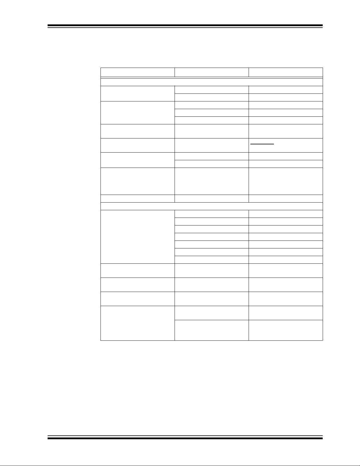
Chapter 1. Product Overview
1.1 INTRODUCTION
This chapter provides an overview of the MCP1012 1W Demonstration Board and
covers the following topics:
• MCP1012 Short Overview(1)
• MCP1012 1W Demonstration Board Description
• Contents of the MCP1012 1W Demonstration Board Kit
MCP1012
1W DEMONSTRATION BOARD
USER’S GUIDE
1.2 MCP1012 SHORT OVERVIEW
1.2.1 Features
• High Voltage Start-Up (rated 500V/700V)
• Internal Open-Loop, Peak Current Mode, Current Regulator for Start-Up
• Current Regulator Constant 21.0 µs OFF Time
• Programmable Low Frequency Oscillator (LFO) Period
• Cycle-by-Cycle Current Limiting
• Protection against Continuous Conduction Mode (CCM) of Operation
• Able to Accept External PWM Commands from a Secondary-Side Controller via
Isolator (Optocoupler or Pulse Transformer)
• Undervoltage Lockout (UVLO) and Overvoltage Lockout (OVLO) Protections
• Sleep and Wake-Up Commands
• Robust Gate Driver, able to drive 2.2 nF Load at 65 kHz
• Overtemperature Protection (Thermal Shutdown)
• Package: 7-Lead SOIC
• Environmentally Friendly, EU RoHS Compliant, Pb-Free
1.2.2 Description
The MCP1012 is used as a primary-side start-up IC for starting an off-line Switch Mode
Power Converter, exemplified in this user’s guide and the data sheet by a Flyback
converter.
(1)
The primary functions of the MCP1012 are:
• Starting-Up the Flyback Converter using an Internal Open-Loop, Peak Current
Mode, Current Regulator
• Accepting PWM commands via optocoupler or pulse transformer from a
Secondary-Side Controller
• Providing undervoltage (UVLO) and overvoltage (OVLO) protection
• Peak cycle-by-cycle current limiting when either under control of its internal
current regulator or under control of the Secondary-Side Controller
• Overtemperature protection
Note 1: More detailed information regarding the capabilities of the MCP1012 is
available in the data sheet.
2020 Microchip Technology Inc. DS50002932A-page 9
Page 10
MCP1012 1W Demonstration Board User’s Guide
AC LINE
INTERFACE
GNDLFO
V
DD
V
IN
GATE
C/S
PULSE
MCP1012
C2
D1
D2
D3
T1
Q1
C3
R1
R2
C4
SERIES
REGULATOR
C1
LOAD
FIGURE 1-1: MCP1012 Typical Application — in an Open Loop Flyback Topology.
1.3 MCP1012 1W DEMONSTRATION BOARD DESCRIPTION
The MCP1012 1W Demonstration Board is used to evaluate and demonstrate
Microchip Technology’s MCP1012 product. This board demonstrates the capabilities of
the MCP1012 in a Flyback converter application supplied from an external voltage
source (120V–500V), with regulated output.
DS50002932A-page 10 2020 Microchip Technology Inc.
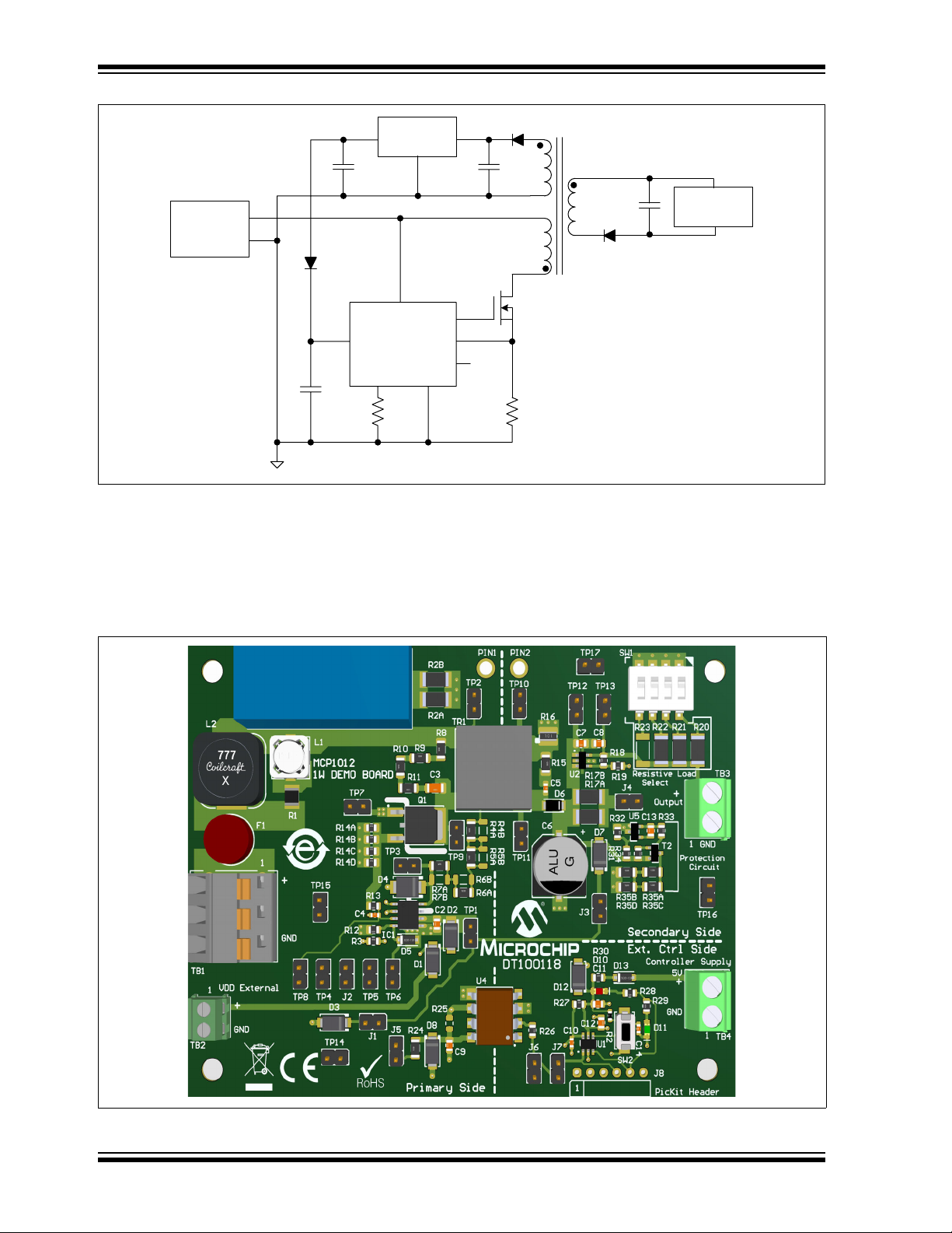
FIGURE 1-2: MCP1012 1W Demonstration Board Top View.
Page 11

Product Overview
1.4 CONTENTS OF THE MCP1012 1W DEMONSTRATION BOARD KIT
The MCP1012 1W Demonstration Board kit includes:
• MCP1012 1W Demonstration Board (DT100118)
• Isolated Jumper JP1 (Mechanical hardware jumper 6.35 mm 1x2 D3087-98)
• Important Information Sheet
2020 Microchip Technology Inc. DS50002932A-page 11
Page 12

MCP1012 1W Demonstration Board User’s Guide
NOTES:
DS50002932A-page 12 2020 Microchip Technology Inc.
Page 13

Chapter 2. Installation and Operation
2.1 GETTING STARTED
In order to use and evaluate the capabilities of the MCP1012, several hardware tools
are required and several guidelines will be followed.
2.1.1 Required Hardware Tools
• MCP1012 1W Demonstration Board (DT100118)
• 120–500 VDC, min. 0.5A DC HV power supply
• 15.0 VDC, min. 0.5A DC power supply
• 5.0 VDC, min. 100 mA DC power supply (only for Sleep/Wake-Up functions
testing)
• DC Voltmeter
• Jumpers (2.54 mm)
• Oscilloscope (optional)
• Signal Generator (optional)
MCP1012
1W DEMONSTRATION BOARD
USER’S GUIDE
2.1.2 Recommendations before Starting the Setup Process
• Place the MCP1012 1W Demonstration Board on a non-conductive surface
when connected to the DC power supplies.
• Do not come into contact with the demonstration board while it is connected to
the DC HV power supply.
• Disconnect the demonstration board from the DC power supplies before
performing any work on the MCP1012 1W Demonstration Board.
• Connect instruments that have earth-referenced inputs (such as most
oscilloscopes) only if the galvanic separation is present against the AC mains, or
use a 1:1 transformer for supplying the demonstration board.
Failure to adhere to these guidelines may result in damage to the demo unit, the tests
instruments, and/or can put in danger the person conducting the tests.
2.2 SETUP PROCEDURE
The functionality of the MCP1012 1W Demonstration Board can be evaluated through
seven different setups, which are described in the following chapters.
2020 Microchip Technology Inc. DS50002932A-page 13
Page 14

MCP1012 1W Demonstration Board User’s Guide
NOTES:
DS50002932A-page 14 2020 Microchip Technology Inc.
Page 15

MCP1012
1W DEMONSTRATION BOARD
USER’S GUIDE
Chapter 3. Setup One
3.1 SETUP 1A
INTRODUCTION
This setup will show the functioning of the MCP1012 in Start-Up mode when it is
supplied by the secondary side of the transformer and no load is applied at the output
(neither of the R20, R21, R22, or R23 resistors is connected).
STEPS
1. Connect/disconnect the jumpers and the switch SW1 according to Ta b le 3 -1 .
TABLE 3-1: STATE OF THE JUMPERS AND SWITCH - SETUP 1A
J1 J2 J3 J4 J5 J6 J7 JP1 SW1.1 SW1.2 SW1.3 SW1.4
ON OFF ON* OFF OFF OFF OFF ON
Note 1: JP1 and J3 connections eliminate the galvanic isolation between the Primary Side
and the Secondary Side of the transformer. Specific safety procedures must be taken
into account. The MCP1012 is supplied from the secondary side of the transformer.
On the board JP1 is connected to PIN1 and PIN2.
1
OFF OFF OFF OFF
2. Connect the voltmeter at the TB3 connector with the positive test probe at the
upper terminal.
3. If available, connect two oscilloscope probes at TP1 (V
output). Connect the ground probes on the primary side, at the TP14 or TP15
Te s t Po in t s .
4. Connect the DC HV power supply in the range of 120–500 VDC at TB1:
- the positive terminal must be connected at the uppermost terminal of the TB1
PCB connector
- the negative terminal must be connected to the bottommost terminal of the TB1
PCB connector (the middle terminal of the TB1 PCB connector is not connected)
5. Read the voltmeter and check if the output voltage of the board is in the range of
4.5V to 5.5V.
6. Check on the oscilloscope screen the V
are presented in Figure 3-1.
voltage and the GATE signal as they
DD
Input) and TP6 (GATE
DD
2020 Microchip Technology Inc. DS50002932A-page 15
Page 16

MCP1012 1W Demonstration Board User’s Guide
FIGURE 3-1: MCP1012 V_GATE and V
Hysteretic Voltage Supply at No
DD
Load.
Note that the MCP1012 is hysteretic supplied, between the OVLO
and OVLO
ON
thresholds.
7. Disconnect the DC HV power supply.
3.2 SETUP 1B
INTRODUCTION
This setup will show the functioning of the MCP1012 in Start-Up mode when it is
supplied by the secondary side of the transformer and a load is applied at the output
(the resistor R21 - 68 is connected through SW1.2)
STEPS
1. Connect/disconnect the jumpers and the switch SW1 according to Ta b le 3 -2 .
TABLE 3-2: THE STATE OF THE JUMPERS AND SWITCH - SETUP 1B
J1 J2 J3 J4 J5 J6 J7 JP1 SW1.1 SW1.2 SW1.3 SW1.4
ON OFF ON
1
OFF OFF OFF OFF ON
Note 1: JP1 and J3 connections eliminate the galvanic isolation between the Primary Side
and the Secondary Side of the transformer. Specific safety procedures must be taken
into account. The MCP1012 is supplied from the secondary side of the transformer.
On the board JP1 is connected to PIN1 and PIN2.
2: SW1.2 is the second switch on the right side of the board.
1
OFF ON
2
OFF OFF
OFF
2. Connect the voltmeter at the TB3 connector with the positive test probe at the
upper terminal.
3. If available, connect two oscilloscope probes at TP1 (V
Input) and TP6 (GATE
DD
output). Connect the ground probes on the primary side, at the TP14 or TP15
Te s t Po in t s .
DS50002932A-page 16 2020 Microchip Technology Inc.
Page 17

Setup One
4. Connect the DC HV power supply in the range of 120–500 VDC at TB1:
- the positive terminal must be connected at the uppermost terminal of the TB1
PCB connector
- the negative terminal must be connected to the bottommost terminal of the TB1
PCB connector (the middle terminal of the TB1 PCB connector is not connected)
5. Read the voltmeter and check if the output voltage of the board is in the range of
4.5V to 5.5V.
6. Check on the oscilloscope screen the V
are presented in Figure 3-2.
.
voltage and the GATE signal as they
DD
FIGURE 3-2: MCP1012 V_GATE and VDD when a Load Is Connected.
7. Disconnect the DC HV power supply.
2020 Microchip Technology Inc. DS50002932A-page 17
Page 18

MCP1012 1W Demonstration Board User’s Guide
NOTES:
DS50002932A-page 18 2020 Microchip Technology Inc.
Page 19

MCP1012
1W DEMONSTRATION BOARD
USER’S GUIDE
Chapter 4. Setup Two
4.1 SETUP 2
INTRODUCTION
This setup will show the functioning of the MCP1012 in Start-Up mode when it is
supplied by an external power supply (15V) at V
output (the resistor R20 - 51 is connected through SW1.1).
A voltage greater than 11.5V on V
pin disables the internal HV regulator.
DD
STEPS
1. Connect/disconnect the jumpers and the switch SW1 according to Ta b le 4 -1 .
TABLE 4-1: THE STATE OF THE JUMPERS AND SWITCH - SETUP 2
J1 J2 J3 J4 J5 J6 J7 JP1 SW1.1 SW1.2 SW1.3 SW1.4
ON OFF OFF OFF OFF OFF OFF OFF ON
Note 1: SW1.1 is the first switch on the right side of the board.
pin and a load is applied at the
DD
1
OFF OFF OFF
2. Connect the voltmeter at the TB3 connector with the positive test probe at the
upper terminal.
3. If available, connect two oscilloscope probes at TP6 (GATE output) and TP8 (C/S
input). Connect the ground probes on the primary side, at the TP14 or TP15 Test
Points.
4. Connect the DC power supply 15V at the TB2 connector:
- the positive terminal must be connected at the upper terminal of the TB2 PCB
connector
- the negative terminal must be connected to the bottom terminal of the TB2 PCB
connector
5. Connect the DC HV power supply in the range of 120–500 VDC at the TB1
connector:
- the positive terminal must be connected at the uppermost terminal of the TB1
PCB connector
- the negative terminal must be connected to the bottommost terminal of the TB1
PCB connector (the middle terminal of the TB1 PCB connector is not connected)
6. Read the voltmeter and check if the output voltage of the board is in the range of
4.5V to 5.5V.
2020 Microchip Technology Inc. DS50002932A-page 19
Page 20

MCP1012 1W Demonstration Board User’s Guide
7. Check on the oscilloscope screen the V_GATE voltage and the C/S signal, as
they are presented in Figure 4-1.
FIGURE 4-1: MCP1012 V_GATE and C/S Voltage.
During the Leading Edge Blanking (LEB) period the spikes on C/S pin are ignored. After
LEB, once the C/S voltage reaches the threshold of 125 mV, the GATE signal is
inhibited.
8. Check on the oscilloscope screen the V_GATE voltage, as it is presented in
Figure 4-2. Set the oscilloscope accordingly.
FIGURE 4-2: MCP1012 V_GATE Voltage.
The value of the resistor connected to LFO pin is 47.5 k. This value conducts to an
LFO period of 1.06 ms or a frequency of 943 Hz. On each LFO period, a number of 16
pulses can be seen.
DS50002932A-page 20 2020 Microchip Technology Inc.
Page 21

Setup Two
9. Check on the oscilloscope screen the V_GATE voltage, as it is presented in the
Figure 4-3. Set the oscilloscope accordingly.
FIGURE 4-3: MCP1012 V_GATE Voltage, t
After V_GATE signal is inhibited, t
10. Disconnect the DC power supplies.
has a constant interval of 21.0 µs.
OFF
OFF
Interval.
2020 Microchip Technology Inc. DS50002932A-page 21
Page 22

MCP1012 1W Demonstration Board User’s Guide
NOTES:
DS50002932A-page 22 2020 Microchip Technology Inc.
Page 23

MCP1012
1W DEMONSTRATION BOARD
USER’S GUIDE
Chapter 5. Setup Three
5.1 SETUP 3
INTRODUCTION
This setup will show the Sleep/Wake-Up functions of the MCP1012 in Start-Up mode
when it is supplied by an external power supply (15V) at V
at the output (the resistor R20 - 51 is connected through SW1.1).
The Sleep/Wake-Up functions are active in both Start-Up and Normal Run mode.
STEPS
1. Connect/disconnect the jumpers and the switch SW1 according to Ta b le 5 -1 .
TABLE 5-1: THE STATE OF THE JUMPERS AND SWITCH - SETUP 3
J1 J2 J3 J4 J5 J6 J7 JP1 SW1.1 SW1.2 SW1.3 SW1.4
ON OFF OFF OFF ON OFF ON OFF ON
Note 1: SW1.1 is the first switch on the right side of the board.
1
pin and a load is applied
DD
OFF OFF OFF
2. Connect the voltmeter at the TB3 connector with the positive test probe at the
upper terminal.
3. If available, connect two oscilloscope probes at TP6 (GATE output) and TP4
(PULSE input). Connect the ground probes on the primary side, at the TP14 or
TP15 Test Points.
4. Connect the DC power supply 15V at the TB2 connector:
- the positive terminal must be connected at the upper terminal of the TB2 PCB
connector
- the negative terminal must be connected to the bottom terminal of the TB2 PCB
connector
5. Connect the DC power supply 5.0V at the TB4 connector:
- the positive terminal must be connected at the upper terminal of the TB4 PCB
connector
- the negative terminal must be connected to the bottom terminal of the TB4 PCB
connector
6. Connect a DC HV power supply in the range of 120–500 VDC at the TB1
connector:
- the positive terminal must be connected at the uppermost terminal of the TB1
PCB connector
- the negative terminal must be connected to the bottommost terminal of the TB1
PCB connector (the middle terminal of the TB1 PCB connector is not connected)
7. Read the voltmeter and check if the output voltage of the board is in the range of
4.5V to 5.5V.
2020 Microchip Technology Inc. DS50002932A-page 23
Page 24

MCP1012 1W Demonstration Board User’s Guide
8. Push the push button SW2 and check on the oscilloscope screen the V_GATE
voltage and the PULSE signal, as they are presented in Figure 5-1 and
Figure 5-2.
FIGURE 5-1: MCP1012 Sleep Command.
Five pulses applied on PULSE pin negative edge at 500 kHz activate the Sleep
function of the MCP1012.
FIGURE 5-2: MCP1012 Sleep Command (Figure 5-1 Detail).
9. Read the voltmeter and check if the output voltage is 0V.
DS50002932A-page 24 2020 Microchip Technology Inc.
Page 25

Setup Three
10. Push the push button SW2 again and check on the oscilloscope screen if the
V_GATE voltage and the PULSE signal are as they are presented in Figure 5-3
and Figure 5-4.
FIGURE 5-3: MCP1012 Wake-Up Command.
The Wake-Up command consists of a single valid PWM Pulse.
FIGURE 5-4: MCP1012 Wake-Up Command (Figure 5-3 Detail).
If the external PWM signal ceases for a period greater than 260 μs typical, then the
gate driver will be driven by the internal current regulator (return to Start-Up mode).
11. Read the voltmeter and check if the output voltage of the board is in the range of
4.5V to 5.5V.
12. Disconnect the DC power supplies.
2020 Microchip Technology Inc. DS50002932A-page 25
Page 26

MCP1012 1W Demonstration Board User’s Guide
NOTES:
DS50002932A-page 26 2020 Microchip Technology Inc.
Page 27

6.1 SETUP 4A
INTRODUCTION
STEPS
MCP1012
1W DEMONSTRATION BOARD
USER’S GUIDE
Chapter 6. Setup Four
This setup will show the functioning of the MCP1012 in Normal Run mode when an
external command is applied at PULSE pin and the C/S pin voltage does not reach the
COMP1 Reference (252 mV).
When a valid PWM signal in the 20-65 kHz frequency range is detected on the PULSE
pin and the internal HV regulator is turned off by applying a voltage greater than 11.5V
typical on the V
pin and not by the internal signal. The COMP1 Reference threshold during external
command switches from 125 mV to 252 mV typical.
pin, the MCP1012’s gate driver is driven by the signal at the PULSE
DD
1. Connect/disconnect the jumpers and the switch SW1 according to Ta b le 6 -1 .
TABLE 6-1: THE STATE OF THE JUMPERS AND SWITCH - SETUP 4A
J1 J2 J3 J4 J5 J6 J7 JP1 SW1.1 SW1.2 SW1.3 SW1.4
ON OFF OFF OFF ON OFF OFF OFF OFF OFF OFF OFF
2. Connect at the jumper J4 an external load consisting of a 10, min. 3W resistor.
3. Connect at the jumper J6 the output of the signal generator with the next setup:
square waveform, minimum voltage 0V, maximum voltage +5.0V, frequency
20 kHz, duty cycle 75%.
4. Connect three oscilloscope probes at TP4 (PULSE input), TP6 (GATE output),
and TP8 (C/S input). Connect the ground probes on the primary side, at the TP14
or TP15 Test Points.
5. Connect a DC power supply 15V at the TB2 connector:
- the positive terminal must be connected at the upper terminal of the TB2 PCB
connector
- the negative terminal must be connected to the bottom terminal of the TB2 PCB
connector
6. Connect a 120 VDC DC HV power supply at TB1:
- the positive terminal must be connected at the uppermost terminal of the TB1
PCB connector
- the negative terminal must be connected to the bottommost terminal of the TB1
PCB connector (the middle terminal of the TB1 PCB connector is not connected)
7. Activate the output of the signal generator
2020 Microchip Technology Inc. DS50002932A-page 27
Page 28

MCP1012 1W Demonstration Board User’s Guide
8. Check on the oscilloscope screen the signals V_PULSE, V_GATE and V_C/S as
they are presented in Figure 6-1
FIGURE 6-1: V_PULSE, V_GATE and V_CS when COMP1 Reference Is Not Reached.
When a valid PWM signal in the 20–65 kHz frequency range is applied the MCP1012’s
gate driver is driven by the signal at the PULSE pin and not by the internal signal. The
COMP1 Reference threshold during external command switches from 125 mV to
252 mV typical.
9. Disconnect the DC power supplies.
10. Disconnect the load at J4.
6.2 SETUP 4B
INTRODUCTION
This setup will show the functioning of the MCP1012 in Normal Run mode when an
external command is applied at PULSE pin and the C/S pin voltage reaches the
COMP1 Reference (252 mV).
STEPS
1. Connect/disconnect the jumpers and the switch SW1 according to Ta b le 6 -2 .
TABLE 6-2: THE STATE OF THE JUMPERS AND SWITCH - SETUP 4B
J1 J2 J3 J4 J5 J6 J7 JP1 SW1.1 SW1.2 SW1.3 SW1.4
ON OFF OFF OFF ON OFF OFF OFF OFF OFF OFF OFF
2. Connect at the jumper J4 an external load consisting of a 10, min 3W resistor.
3. Connect at the jumper J6 the output of the signal generator with the next setup:
square waveform, minimum voltage 0V, maximum voltage +5.0V, frequency
20 kHz, duty cycle 30%.
4. Connect three oscilloscope probes at TP4 (PULSE input), TP6 (GATE output),
and TP8 (C/S input). Connect the ground probes on the primary side, at the TP14
or TP15 Test Points.
5. Connect a DC power supply 15V at the TB2 connector:
DS50002932A-page 28 2020 Microchip Technology Inc.
Page 29

Setup Four
- the positive terminal must be connected at the upper terminal of the TB2 PCB
connector
- the negative terminal must be connected to the bottom terminal of the TB2 PCB
connector
6. Connect a 120 VDC DC HV power supply at TB1:
- the positive terminal must be connected at the uppermost terminal of the TB1
PCB connector
- the negative terminal must be connected to the bottommost terminal of the TB1
PCB connector (the middle terminal of the TB1 PCB connector is not connected)
7. Activate the output of the signal generator.
8. Check on the oscilloscope screen the signals V_PULSE, V_GATE, and V_C/S
as they are presented in Figure 6-2.
FIGURE 6-2: V_PULSE, V_GATE, and V_CS when the COMP1 Reference Is Reached.
When the voltage on the C/S pin reaches the COMP1 reference (typ. 252 mV), the
Gate command is turned off even if the PULSE logic state is Low.
9. Disconnect the DC power supplies.
2020 Microchip Technology Inc. DS50002932A-page 29
Page 30

MCP1012 1W Demonstration Board User’s Guide
NOTES:
DS50002932A-page 30 2020 Microchip Technology Inc.
Page 31

MCP1012
1W DEMONSTRATION BOARD
USER’S GUIDE
Chapter 7. Setup Five
7.1 SETUP 5
INTRODUCTION
This setup will show the functioning of the MCP1012 in Start-Up mode when a short
circuit is created on the secondary side of the transformer.
STEPS
1. Connect/disconnect the jumpers and the switch SW1 according to Ta b le 7 -1 .
TABLE 7-1: THE STATE OF THE JUMPERS AND SWITCH - SETUP 5
J1 J2 J3 J4 J5 J6 J7 JP1 SW1.1 SW1.2 SW1.3 SW1.4
ON OFF OFF ON OFF OFF OFF ON
Note 1: JP1 connection eliminates the galvanic isolation between the Primary Side and the
Secondary Side of the transformer. Specific safety procedures must be taken into
account.
2: SW1.1 is the first switch on the right side of the board.
1
ON
2
OFF OFF OFF
2. Connect a voltmeter at the TB3 connector with the positive test probe at the
upper terminal.
3. If available, connect two oscilloscope probes at TP6 (GATE output) and TP12.
Connect the ground probes on the primary side, at the TP14 or TP15 Test Points.
4. Connect a DC power supply 15V at the TB2 connector:
- the positive terminal must be connected at the upper terminal of the TB2 PCB
connector
- the negative terminal must be connected to the bottom terminal of the TB2 PCB
connector
5. Connect a DC HV power supply in the range of 120–500 VDC at the TB1
connector:
- the positive terminal must be connected at the uppermost terminal of the TB1
PCB connector
- the negative terminal must be connected to the bottommost terminal of the TB1
PCB connector (the middle terminal of the TB1 PCB connector is not connected)
6. Read the voltmeter and check if the output voltage of the board is 0V.
2020 Microchip Technology Inc. DS50002932A-page 31
Page 32

MCP1012 1W Demonstration Board User’s Guide
7. Check on the oscilloscope screen the V_GATE voltage during the short circuit
condition as it is presented in Figure 7-1.
FIGURE 7-1: MCP1012 V_GATE Voltage during a Short Circuit Condition.
8. Disconnect the DC power supplies.
9. Disconnect the jumper J4.
10. Reconnect the DC power supplies.
Check the functionality of the MCP1012 by running the setups described in this user’s
guide.
DS50002932A-page 32 2020 Microchip Technology Inc.
Page 33

Appendix A. Schematic and Layouts
A.1 INTRODUCTION
This appendix contains the following schematic and layouts for the MCP1012 1W
Demonstration Board:
• Board – Schematic
• Board – Top Silk
• Board – Top Copper and Silk
• Board – Top Copper
• Board – Bottom Copper
• Board – Bottom Copper and Silk
• Board – Bottom Silk
MCP1012
1W DEMONSTRATION BOARD
USER’S GUIDE
2020 Microchip Technology Inc. DS50002932A-page 33
Page 34

DS50002932A-page 34 2020 Microchip Technology Inc.
GND GND
GND
GND
2.49K
1206
1%
R4A
2.49K
1206
1%
R5A
2.49K
1206
1%
R6A
2.49K
1206
1%
R7A
2.49K
1206
1%
R8
2.49K
1206
1%
R9
2.49K
1206
1%
R10
2.49K
1206
1%
R11
1R
0805
5%
R12
10R
0805
1%
R13
0.1R
0805
1%
DNP
R14C
0.1R
0805
1%
DNP
R14D
GND
330pF
200V
0603
C5
10R
1206
5%
R15
0.05R
0612
1%
R16
GNDS
1R
2010
1%
R17A
1R
2010
1%
R17B
330k
0805
1%
R18
100k
0805
5%
R19
68R
2010
5%
R21
220R
2010
5%
R22
VDD
GND
1 8
2 7
3 6
4 5
SW1
220R
2010
5%
R23
GND
BAT46W
D5
VDD
7
10
2
5
SEC
7.5V-200mA
6
8
120-375Vdc
20kHz
1
4
750318391
TR1
12
HDR-2.54 Male 1x2
J3
2.2uF
16V
0805
C8
1 2
HDR-2.54 Male 1x2
J4
12
HDR-2.54 Male 1x2
TP5
12
TP14
GND
12
HDR-2.54 Male 1x2
J2
GND
GND
12
TERMINAL 1x2
TB2
VDD_EXT
GND
12
TP2
1 2
TP1
1 2
TP4
1 2
TP3
12
TP6
12
TP7
12
TP8
12
TP9
1 2
TP10
12
TP11
12
TP12
12
TP13
GND
12
TP1512TP1612TP17
SMAJ22A
D3
GND
P6KE510
D4
GND
1uF
50V
0805
C7
330uF
50V
CAP_AL_G
C6
47k
0805
1%
R3
1.5R
0805
1%
R14A
1.6R
0805
1%
R14B
US1M
D1
US1M
D2
US1M
D7
RED
D10
GREEN
D11
0.1uF
50V
0805
C11
680R
0805
1%
R28
560R
0805
R29
10R
R30
10000pF
C10
12
EG4576
SW2
100k
R27
5.1V
D12
12
HDR-2.54 Male 1x2
J5
GNDGND
GND
390R
0805
5%
DNP
R25
12
HDR-2.54 Male 1x2
J7
12
HDR-2.54 Male 1x2
J6
GNDSIG
External PWM drive
1 2
TERMINAL 1x2
TB4
External 5V Supply
330R
1206
5%
R24
DC Input Voltage
(+)
(-)
1 2
TERMINAL 1x2
TB3
1
2
3
TERMINAL 1x3
TB1
(NC)
3
NC
4
2
GND
5
6
NC
7
VCC8NC
1
HCPL-2202
U4
1.5k
0805
1%
R26
0R
1206
DNP
R4B
0R
1206
DNP
R5B
0R
1206
DNP
R6B
0R
1206
DNP
R7B
2A
P5.08D8.5H8
F1
18V
D8
0.47uF
50V
0805
C9
3 2
1
TLV431A-D
U5
1
2
3
BC807
T2
18k
0805
1%
R31
4.7k
0805
5%
R33
5.6k
0805
1%
R34
1.3k
0805
1%
R32
1000pF
50V
0805
C13
330R
1206
5%
R35A
330R
1206
5%
R35B
330R
1206
5%
R35C
330R
1206
5%
R35D
1 2
J1
TB = Terminal Block
TP = Test Point
J = Jumper
D3087-98
JP1
1
H3185-05
PIN1
1
H3185-05
PIN2
JP1 is a link between PIN1 and PIN2
2R
2010
5%
R2A
2R
2010
5%
R2B
1500uH
L2
1.5R
1210
1%
R1
2
1
3
IPD90R1K2C3ATMA1
Q1
GATE
4
GND
5
VDD
6
VIN
8
PULSE
1
LFO
2
C/S
3
MCP1012
IC1
GNDS GNDS
GNDS
GNDS
GNDS
GNDS GNDS GNDS
GNDS
GNDSIG
GNDSIG
GNDSIG
GNDSIG GNDSIG GNDSIG GNDSIG
GNDSIG
GNDS GNDS
LABEL Need Help Small
LABEL1
RUBBER PAD 0.50x0.50x0.23
PAD1
RUBBER PAD 0.50x0.50x0.23
PAD2
RUBBER PAD 0.50x0.50x0.23
PAD3
RUBBER PAD 0.50x0.50x0.23
PAD4
2.2uF
C1
1uF
50V
0805
C2
1000pF
2KV
C3
330pF
50V
0603
C4
51R
2010
5%
R20
100uH
L1
DFLS1200-7
D6
1N4148
D13
10uF
10V
0805
C12
MCLR
PICKIT HEADER
ICSPCLK
ICSPDAT
HDR-2.54 Male 1x6
123456
J8
PIC_VDD
PIC_VDD
GNDSIG
PIC_VDD
Switch
10k
0603
1%
R2
PIC_VDD
MCLR
MCLR
ICSPCLK
ICSPDAT
ICSPDAT
ICSPCLK
Switch
GNDSIG
1000pF
50V
0603
C14
RA0/ICSPDAT
1
VSS
2
RA1/ICSPCLK
3
RA2
4
VDD
5
RA3/MCLR/VPP
6
T
VSS
K
V
P
PIC10F322
U1
IN
1
GND
2
EN3NC/ADJ
4
OUT
5
IN
D
EN
O
MIC5235YM5
U2
A.2 BOARD – SCHEMATIC
MCP1012 1W Demonstration Board User’s Guide
UT
NC/ADJ
N
RA0/ICSPDA
RA1/ICSPCL
R
RA3/MCLR/VP
DD
Page 35

A.3 BOARD – TOP SILK
Schematic and Layouts
A.4 BOARD – TOP COPPER AND SILK
2020 Microchip Technology Inc. DS50002932A-page 35
Page 36

MCP1012 1W Demonstration Board User’s Guide
A.5 BOARD – TOP COPPER
A.6 BOARD – BOTTOM COPPER
DS50002932A-page 36 2020 Microchip Technology Inc.
Page 37

A.7 BOARD – BOTTOM COPPER AND SILK
Schematic and Layouts
A.8 BOARD – BOTTOM SILK
2020 Microchip Technology Inc. DS50002932A-page 37
Page 38

MCP1012 1W Demonstration Board User’s Guide
NOTES:
DS50002932A-page 38 2020 Microchip Technology Inc.
Page 39

MCP1012
1W DEMONSTRATION BOARD
USER’S GUIDE
Appendix B. Bill of Materials (BOM)
TABLE B-1: BILL OF MATERIALS (BOM)
Qty. Reference Description Manufacturer Part Number
1 C1 Capacitor, film, 2.2 µF 305
VAC 20% radial
P27.5L31.5W14H24.5
2 C2, C7 Capacitor, ceramic, µF 50V
10% X7R, surface mount, 0805
1 C3 Capacitor, ceramic, 1000 pF
2KV 10% X7R surface mount,
1206
1 C4 Capacitor, ceramic, 330 pF
50V 5% C0G surface mount,
0603
1 C5 Capacitor, ceramic, 330 pF
200V 10% X7R surface mount,
0603
1 C6 Capacitor, Alu., 330 µF 50V
20% surface mount, G
1 C8 Capacitor, ceramic, 2.2 µF 16V
10% X7R surface mount, 0805
1 C9 Capacitor, ceramic, 0.47 µF 50V
10% X7R surface mount, 0805
1 C10 Capacitor, ceramic, 10000 pF
25V 10% X7R surface mount,
0603
1 C11 Capacitor, ceramic, 0.1 µF 50V
10% X7R, surface mount,
0805
1 C12 Capacitor, ceramic, 10 µF 10V
10% X5R, surface mount,
0805
1 C13 Capacitor, ceramic, 1000 pF
50V 10% X7R, surface mount,
0805
1 C14 Capacitor, ceramic, 1000 pF
50V 20% X7R, surface mount,
0603
3 D1, D2, D7 Diode, rectifier, US1M 1.7V 1A
1000V DO-214AC_SMA
1 D3 Diode, TVS, SMAJ22A 22V
400W SMD DO-214AC_SMA
1 D4 Diode, TVS, P6KE510 434V
600W DO-214AA_SMB
1 D5 Diode, Schottky, BAT46W-TP
450 mV 10 mA 100V, surface
mount, SOD-123
EPCOS AG B32924C3225M
Murata Electronics
America, Inc.
Johanson Dielectrics Inc. 202R18W102KV4E
KEMET C0603C331J5GACTU
KEMET C0603C331K2RAC7867
Panasonic Electronic
Components
Murata Electronics
America, Inc
Murata Electronics
America, Inc
Panasonic
Cal-Chip Electronics Inc. GMC21X7R104K50NTLF
Taiyo Yuden Co., Ltd. LMK212BJ106KG-T
Murata Electronics North
America
TDK Corporation C1608X7R2A102K080AA
Vishay Dale US1M-E3/61T
Bourns
Micro Commercial
Components Corp. (MCC)
Micro Commercial
Components Corp. (MCC)
®
®
, Inc. SMAJ22A
North
North
North
- ECG ECJ-1VB1E103K
GRM21BR71H105KA12L
EEE-FT1H331AP
GRM21BR71C225KA12L
GRM21BR71H474KA88L
GRM216R71H102KA01D
SMBJP6KE510A-TP
BAT46W-TP
2019 Microchip Technology Inc. DS50002932A-page 39
Page 40

MCP1012 1W Demonstration Board User’s Guide
TABLE B-1: BILL OF MATERIALS (BOM) (CONTINUED)
Qty. Reference Description Manufacturer Part Number
1 D6 Diode, Schottky, DFLS1200-7
850 mV 1A 200V POWERDI-123
1 D8 Diode, zener, SMAZ18-13-F
18V 1W DO-214AC_SMA
1 D10 Diode, LED, red 2.2V 20 mA
40 mcd, clear, surface mount,
0805
1 D11 Diode, LED, green, 3.1V 20 mA
400 mcd, clear, surface mount,
0805
1 D12 Diode, zener SMAZ5V1-13-F
5.1V 1W DO-214AC_SMA
1 D13 Diode, rectifier, 1N4148 1.25V
150 mA 100V SOD-123
1 F1 Resistor, fuse, 2A 300 VAC,
Slow, radial, TH P5.08D8.5H8
1 IC1 IC MCP1012 SOIC-8 Microchip Technology Inc. MCP1012-V/EKA
24 J1, J2, J3, J4,
J5, J6, J7, TP1,
TP2, TP3, TP4,
TP5, TP6, TP7,
TP8, TP9,
TP10, TP11,
TP12, TP13,
TP14, TP15,
TP16, TP17
1 JP1 Mechanical, hardware, jumper,
1 L1 Inductor, 100 µH 0.79A 20%,
1 LABEL1 Label, assembly with rev. level
1 L2 Inductor 1500 µH 810 mA
4PAD1, PAD2,
PAD3, PAD4
1PCB1
2 PIN1, PIN2 Connector, receptacle, 1pin AU
1 Q1 Transistor FET N-Channel
1 R1 Resistor, TKF 1.5R 1% 1/3W,
1 R2 Resistor, TF 10k 1% 1/16W
2 R2A, R2B Resistor, TKF 2R 5% 3/4W,
Connector, header-2.54 male
1x2 Gold 5.84 MH TH, vertical
6.35 mm 1x2 D3087-98
surface mount, L7.3W7.3H4.5
(small modules) per MTS-0002
10%, surface mount,
L12.3W12.3H10
Mechanical, hardware, rubber
pad, SQ, taper 0.50x0.50x0.23
black
MCP1012 Demonstration
Board - printed circuit board
H3185-05 THT
IPD90R1K2C3ATMA1 900V
5.1A 1.2R 83W TO-252-3
surface mount, 1210
surface mount, 0603
surface mount, 2010
Diodes Incorporated
Diodes Incorporated SMAZ18-13-F
Dialight Corporation 598-8110-107F
QT-Brightek Corporation
(QTB)
Diodes Incorporated SMAZ5V1-13-F
Micro Commercial
Components Corp. (MCC)
Littelfuse
Amphenol Commercial 77311-118-02LF
Harwin Plc. D3087-98
Wurth Electronik 744777920
——
Coilcraft MSS1210-155KEB
3M SJ-5518
Microchip Technology Inc.
Harwin Plc. H3185-05
Infineon Technologies AG IPD90R1K2C3ATMA1
Stackpole Electronics, Inc. RMCF1210FT1R50
TE Connectivity CPF0603F10KC1
Panasonic - ECG ERJ-12ZYJ2R0U
®
®
DFLS1200-7
QBLP631-IG
1N4148W-TP
38312000000
04-11027-R1
DS50002932A-page 40 2019 Microchip Technology Inc.
Page 41

Bill of Materials (BOM)
TABLE B-1: BILL OF MATERIALS (BOM) (CONTINUED)
Qty. Reference Description Manufacturer Part Number
1 R3 Resistor, TKF 47k 1% 1/8W,
surface mount, 0805
8 R4A, R5A, R6A,
R7A, R8, R9,
R10, R11
1 R12 Resistor, TKF 1R 5% 1/8W,
2 R13, R30 Resistor, TKF 10R 1% 1/8W,
1 R14A Resistor, TKF 1.5R 1% 1/8W,
1 R14B Resistor, TKF 1.6R 1% 1/8W,
1 R15 Resistor, TKF 10R 5% 1/4W,
1 R16 Resistor, TF 0.05R 1% 1W,
2 R17A, R17B Resistor, TKF 1R 1% 3/4W,
1 R18 Resistor, TKF 330k 1% 1/8W,
2 R19, R27 Resistor, TKF 100k 5% 1/8W,
1 R20 Resistor, TKF 51R 5% 3/4W,
1 R21 Resistor, TKF 68R 5% 3/4W,
1 R22 Resistor, TKF 220R 5% 3/4W,
5 R24, R35A,
R35B, R35C,
R35D
1 R26 Resistor, TKF 1.5k 1% 1/8W,
1 R28 Resistor, TKF 680R 1% 1/8W,
1 R29 Resistor, TKF 560R 1% 1/8W,
1 R31 Resistor, TKF 18k 1% 1/8W,
1 R32 Resistor, TKF 1.3k 1% 1/8W,
1 R33 Resistor, TKF 4.7k 5% 1/8W
1 R34 Resistor, TKF 5.6k 1% 1/8W,
1 SW1 Switch, DIP 4 SPST 24V
Resistor, TKF 2.29k 1% 1/4W,
surface mount, 1206
surface mount, 0805
surface mount, 0805
surface mount, 0805
surface mount, 0805 AEC-Q200
surface mount, 1206
surface mount, 0612
surface mount, 2010
surface mount, 0805 AEC-Q200
surface mount, 0805
surface mount, 2010
surface mount, 2010
surface mount, 2010
Resistor, TKF 330R 5% 1/4W,
surface mount, 1206
surface mount, 0805
surface mount, 0805
surface mount, 0805
surface mount, 0805
surface mount, 0805
surface mount, 0805
surface mount, 0805
100 mA 1-1825059-3, surface
mount
Stackpole Electronics, Inc. RMCF0805FT47K0
Yageo Corporation RC1206FR-072K49L
Panasonic ERJ-6RQJ1R0V
ROHM Semiconductor MCR10EZHF10R0
TT Electronics ASC0805-1R5FT5
Panasonic ERJ-6RQF1R6V
Yageo Corporation AC1206JR-0710RL
Susumu Co., Ltd PRL1632-R050-F-T1
Vishay Dale CRCW20101R00FKEF
Panasonic ERJ-6ENF3303V
Panasonic ERJ-6GEYJ104V
Panasonic ERJ-12ZYJ510U
Panasonic ERJ-12ZYJ680U
Panasonic ERJ-12ZYJ221U
Panasonic ERJ-8GEYJ331V
Panasonic ERJ-6ENF1501V
Stackpole Electronics, Inc RMCF-1/10-680-1%
Stackpole Electronics, Inc RMCF0805FT560R
Stackpole Electronics, Inc RMCF-1/10-18K-1%
Yageo Corporation RC0805FR-071K3L
Panasonic ERJ-6GEYJ472V
Vishay Dale CRCW08055K60FKEA
TE Connectivity 1-1825059-3
2019 Microchip Technology Inc. DS50002932A-page 41
Page 42

MCP1012 1W Demonstration Board User’s Guide
TABLE B-1: BILL OF MATERIALS (BOM) (CONTINUED)
Qty. Reference Description Manufacturer Part Number
1 SW2 Switch, tact. SPST 12V 50mA
TL3302AF180QJ, surface
mount
1 T2 Transistor, BJT, PNP
BC807-16L -45V -500 mA
225 mW SOT-23-3
1 TB1 Connector, terminal 5.08 mm
1x3 female 16-22AWG 10A TH
R/A
1 TB2 Connector, terminal 3.5 mm
1x2 Female 24-16AWG 10A
TH R/A
1 TB3, TB4 Connector, terminal 5 mm 1x2
female 12-26AWG 18A TH R/A
1 TR1 Transistor, power 12:1 7.5V
200R14C, R14D mA 7.6 mH TH
1 U1 Microchip MCU 8-Bit 16 MHz
918B 64B PIC10F322-I/OT
SOT-23-6
1 U2 Microchip Analog LDO ADJ
MIC5235YM5-TR SOT-23-5
1 U4 IC Optoisolator 3.75 kV 5 Mb
HCPL-2202-300E DIP-8 GW
1 U5 IC Power TLV431BSN1T1G
Shunt Voltage Reference
SOT23-3
Note 1: The components listed in this Bill of Materials are representative of the PCB assembly. The released BOM
used in manufacturing uses all RoHS-compliant components.
E-Switch®, Inc. TL3302AF180QJ
ON Semiconductor
Wurth Electronik 691415520003
Wurth Electronik 691214110002
Phoenix Contact 1935161
Wurth Electronik 750318391
Microchip Technology Inc. PIC10F322-I/OT
Microchip Technology Inc. MIC5235YM5-TR
Broadcom
ON Semiconductor TLV431BSN1T1G
®
®
BC807-16LT1G
HCPL-2202-300E
Table B-2: BILL OF MATERIALS (BOM – DO NOT POPULATE)
Qty. Reference Description Manufacturer Part Number
0 J8 Connector, Header-2.54 male
1x6 gold 5.84 MH TH R/A
DO NOT POPULATE
0R4B, R5B,
R6B, R7B
2 R14C, R14D Resistor, TKF 0.1R 1% 1/8W,
0 R23 Resistor, TKF 220R 5% 3/4W,
0 R25 Resistor, TKF 390R 5% 1/8W,
Note 1: The components listed in this Bill of Materials are representative of the PCB assembly. The released BOM
used in manufacturing uses all RoHS-compliant components.
Resistor, TKF 0R surface
mount 1206
DO NOT POPULATE
surface mount 0805
DO NOT POPULATE
surface mount, 2010
DO NOT POPULATE
surface mount, 0805
DO NOT POPULATE
Amphenol Commercial 68016-106HLF
Yageo Corporation RC1206JR-070RL
Panasonic - ECG ERJ-L06KF10CV
Panasonic - ECG ERJ-12ZYJ221U
Panasonic - ECG ERJ-6GEYJ391V
DS50002932A-page 42 2019 Microchip Technology Inc.
Page 43

Worldwide Sales and Service
AMERICAS
Corporate Office
2355 West Chandler Blvd.
Chandler, AZ 85224-6199
Tel: 480-792-7200
Fax: 480-792-7277
Technical Support:
http://www.microchip.com/
support
Web Address:
www.microchip.com
Atlanta
Duluth, GA
Tel: 678-957-9614
Fax: 678-957-1455
Austin, TX
Tel: 512-257-3370
Boston
Westborough, MA
Tel: 774-760-0087
Fax: 774-760-0088
Chicago
Itasca, IL
Tel: 630-285-0071
Fax: 630-285-0075
Dallas
Addison, TX
Tel: 972-818-7423
Fax: 972-818-2924
Detroit
Novi, MI
Tel: 248-848-4000
Houston, TX
Tel: 281-894-5983
Indianapolis
Noblesville, IN
Tel: 317-773-8323
Fax: 317-773-5453
Tel: 317-536-2380
Los Angeles
Mission Viejo, CA
Tel: 949-462-9523
Fax: 949-462-9608
Tel: 951-273-7800
Raleigh, NC
Tel: 919-844-7510
New York, NY
Tel: 631-435-6000
San Jose, CA
Tel: 408-735-9110
Tel: 408-436-4270
Canada - Toronto
Tel: 905-695-1980
Fax: 905-695-2078
ASIA/PACIFIC
Australia - Sydney
Tel: 61-2-9868-6733
China - Beijing
Tel: 86-10-8569-7000
China - Chengdu
Tel: 86-28-8665-5511
China - Chongqing
Tel: 86-23-8980-9588
China - Dongguan
Tel: 86-769-8702-9880
China - Guangzhou
Tel: 86-20-8755-8029
China - Hangzhou
Tel: 86-571-8792-8115
China - Hong Kong SAR
Tel: 852-2943-5100
China - Nanjing
Tel: 86-25-8473-2460
China - Qingdao
Tel: 86-532-8502-7355
China - Shanghai
Tel: 86-21-3326-8000
China - Shenyang
Tel: 86-24-2334-2829
China - Shenzhen
Tel: 86-755-8864-2200
China - Suzhou
Tel: 86-186-6233-1526
China - Wuhan
Tel: 86-27-5980-5300
China - Xian
Tel: 86-29-8833-7252
China - Xiamen
Tel: 86-592-2388138
China - Zhuhai
Tel: 86-756-3210040
ASIA/PACIFIC
India - Bangalore
Tel: 91-80-3090-4444
India - New Delhi
Tel: 91-11-4160-8631
India - Pune
Tel: 91-20-4121-0141
Japan - Osaka
Tel: 81-6-6152-7160
Japan - Tokyo
Tel: 81-3-6880- 3770
Korea - Daegu
Tel: 82-53-744-4301
Korea - Seoul
Tel: 82-2-554-7200
Malaysia - Kuala Lumpur
Tel: 60-3-7651-7906
Malaysia - Penang
Tel: 60-4-227-8870
Philippines - Manila
Tel: 63-2-634-9065
Singapore
Tel: 65-6334-8870
Taiwan - Hsin Chu
Tel: 886-3-577-8366
Taiwan - Kaohsiung
Tel: 886-7-213-7830
Taiwan - Taipei
Tel: 886-2-2508-8600
Thailand - Bangkok
Tel: 66-2-694-1351
Vietnam - Ho Chi Minh
Tel: 84-28-5448-2100
EUROPE
Austria - Wels
Tel: 43-7242-2244-39
Fax: 43-7242-2244-393
Denmark - Copenhagen
Tel: 45-4450-2828
Fax: 45-4485-2829
Finland - Espoo
Tel: 358-9-4520-820
France - Paris
Tel: 33-1-69-53-63-20
Fax: 33-1-69-30-90-79
Germany - Garching
Tel: 49-8931-9700
Germany - Haan
Tel: 49-2129-3766400
Germany - Heilbronn
Tel: 49-7131-72400
Germany - Karlsruhe
Tel: 49-721-625370
Germany - Munich
Tel: 49-89-627-144-0
Fax: 49-89-627-144-44
Germany - Rosenheim
Tel: 49-8031-354-560
Israel - Ra’anana
Tel: 972-9-744-7705
Italy - Milan
Tel: 39-0331-742611
Fax: 39-0331-466781
Italy - Padova
Tel: 39-049-7625286
Netherlands - Drunen
Tel: 31-416-690399
Fax: 31-416-690340
Norway - Trondheim
Tel: 47-7288-4388
Poland - Warsaw
Tel: 48-22-3325737
Romania - Bucharest
Tel: 40-21-407-87-50
Spain - Madrid
Tel: 34-91-708-08-90
Fax: 34-91-708-08-91
Sweden - Gothenberg
Tel: 46-31-704-60-40
Sweden - Stockholm
Tel: 46-8-5090-4654
UK - Wokingham
Tel: 44-118-921-5800
Fax: 44-118-921-5820
DS50002932A-page 43 2020 Microchip Technology Inc.
05/14/19
 Loading...