

Page 1
HCS512
KEELOQ® Code Hopping Decoder
FEATURES
Security
• Secure storage of Manufacturer’s Code
• Secure sto rage of transmitter’s keys
• Up to four transmitters can be learned
•K
• Normal and secure learning mechanisms
Operating
• 4.0V – 6.0V operation
• 4 MHz external RC oscillator
• Learning indication on LRNOUT
• Auto baud rate detection
• Power saving SLEEP mode
Other
• Stand-alone decoder
• On-chip EEPROM for transmitter storage
• Four binary function outputs–15 functions
• 18-pin DIP/SOIC package
Typical Applications
• Automotive remote entry systems
• Automotive alarm systems
• Automotive immobilizers
• Gate and garage openers
• Electronic door locks
• Identity t okens
• Burglar alarm systems
Compatible Encoders
All KEELOQ encoders and transponders configured for
the following setting:
• PWM modulation format (1/3-2/3)
•T
•10 x TE Header
• 28-bit Serial Number
• 16-bit Synchronization counter
• Discrimination bit s equal to Serial Num ber 8 LSbs
• 66- to 69-bit length code word.
EELOQ
E in the range from 100 µs to 400 µs
code hopping technology
DESCRIPTION
The Microchip Technology Inc. HC S51 2 is a c od e ho pping decoder designed for secure Remote Keyless
Entry (RKE) systems. The HCS512 utilizes the patented K
EELOQ code hopping system and high security
learning mechanisms to make this a canned solution
when used with the HCS en co ders to i mp lem en t a un idirectional remote keyless entry system.
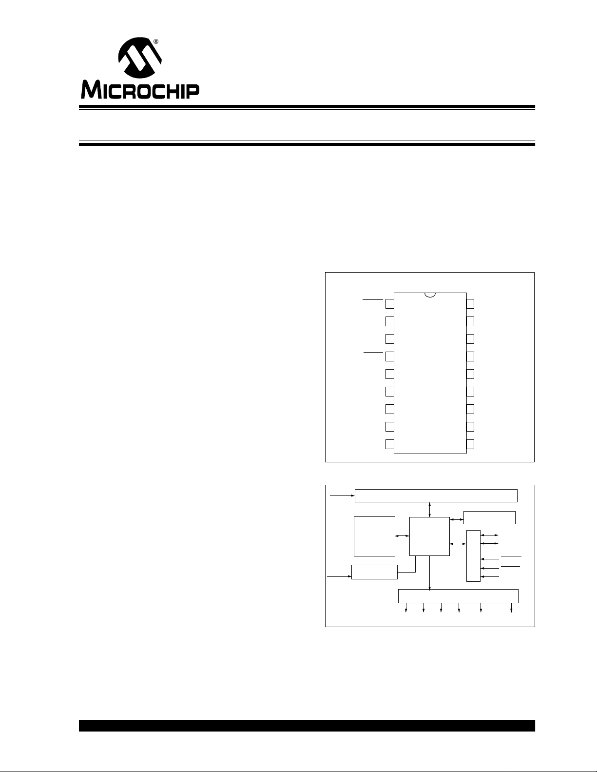
PACKAGE TYPE
PDIP, SOIC
NC
S0
S1
S2
S3
1
2
3
4
5
6
7
8
9
18
RFIN
NC
17
OSCIN
16
HCS512
15
14
13
12
11
10
OSC
VDD
DATA
CLK
SLEEP
V
LOW
OUT
LRNIN
LRNOUT
MCLR
GND
BLOCK DIAGRAM
RFIN
EEPROM CONTROL
OSCIN
OSCILLATOR
The Manufacturer’s Code, transmitter keys, and synchronization information are stored in protected onchip EEPROM. The HCS512 uses the DATA and CLK
inputs to load the Manufacturer’s Code which cannot
be read out of the device.
Reception Register
DECRYPTOR
OUTPUT
S0 S1 S3S2VLOW
CONTROL
DATA
CLK
LRNIN
MCLR
SLEEP
LRNOUT
2002 Microchip Technology Inc. DS40151D-page 1
Page 2

HCS512
The HCS512 operates over a wide voltage range of
3.0 volts to 6.0 volts. The decoder employs automatic
baud rate detection which allows it to compensate for
wide variations in transmitter data rate. The decoder
contains sophisticated error checking algorithms to
ensure only valid codes are accepted.
1.0 SYSTEM OVERVIEW
Key Terms
The following is a l ist of key te rms us ed thro ughout this
data sheet. For additional information on K
Code Hopping, refer to Technical Brief 3 (TB003).
• RKE - Remote Keyless Entry
• Button Status - Indicates what button input(s)
activated the transmission. Encompasses the 4
button status bits S3, S2, S1 and S0 (Figure8-2).
• Code Hopping - A method by which a code,
viewed externally to the system, appears to
change unpredictably each time it is transmitted.
• Code word - A block of data that is repeatedly
transmitted upon button activation (Figure8-1).
• Transmission - A data stream consisting of
repeating code words (Figure 8-1).
• Crypt key - A unique and secret 64-bit number
used to encrypt and decrypt data. In a symmetrical block cipher such as the K
the encryption and de cry pti on k ey s a re equal and
will therefore be refer red to generally as the crypt
key.
• Encoder - A device that generates and encodes
data.
• Encryption Algorithm - A recipe whereb y data i s
scrambled using a crypt k ey . The dat a can only be
interpreted by the respe ctive dec ryptio n algo rithm
using the same crypt key.
• Decoder - A device that decodes data received
from an encoder.
• Decryption algorithm - A recipe whereby data
scrambled by an encryption algorithm can be
unscrambled using the same crypt key.
• Learn – Learning invol ves the recei ver calcula ting
the transmitter’s app ropr i ate crypt key, decrypting
the received hopping code and storing the serial
number, synchronization counter value and crypt
key in EEPROM. The K
itates several learning strategies to be implemented on the decoder. The following are
examples of what can be done.
- Simple Learning
The receiver uses a fixed crypt key, common
to all components of all system s by the s am e
manufacturer, to decrypt the received code
word’s encrypted portion.
- Normal Learning
The receiver uses information transmitted
EELOQ algorithm,
EELOQ product family fa cil-
EELOQ and
during normal operation to derive the crypt
key and decrypt the received code word’s
encrypted portion.
- Secure Learn
The transmitter is activated through a special
button combinat ion to t ransmit a stored 60-bit
seed value used to generat e the trans mitter’s
crypt key. The receiver uses this seed value
to derive the same crypt key and decrypt the
received code word’s encrypted portion.
• Manufacturer’s code – A unique and secret 64-
bit number used to generate un ique encoder crypt
keys. Each encoder is programmed with a crypt
key that is a function of the manufacturer’s code.
Each decoder is programmed with the manufacturer code itself.
1.1 HCS Encoder Overview
The HCS encoders have a small EEPROM array wh ich
must be loaded with several parameters before use.
The most important of these values are:
• A crypt key that is generated at the time of production
• A 16-bit sy nchronizati on counter value
• A 28-bit serial number w hich is meant to be
unique for every encoder
The manufacturer program s the serial nu mber for eac h
encoder at the time of production, while the ‘Key Generation Algorithm’ generat es the crypt k ey (Figure 1-1).
Inputs to the key generation algorithm typically consist
of the encoder’s serial number and a 64-bit manufacturer’s code, which the manufacturer creates.
Note: The manufact urer co de is a pivo tal part of
the system’s overall security. Consequently, all possible precautions must be
taken and maintained for this code.
DS40151D-page 2 2002 Microchip Technology Inc.
Page 3
HCS512
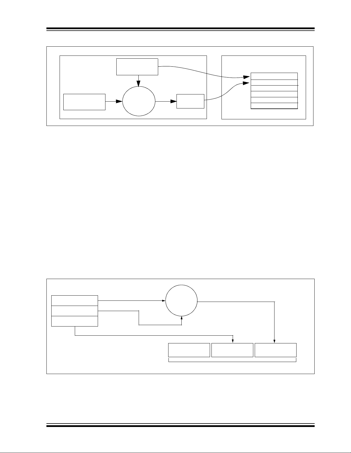
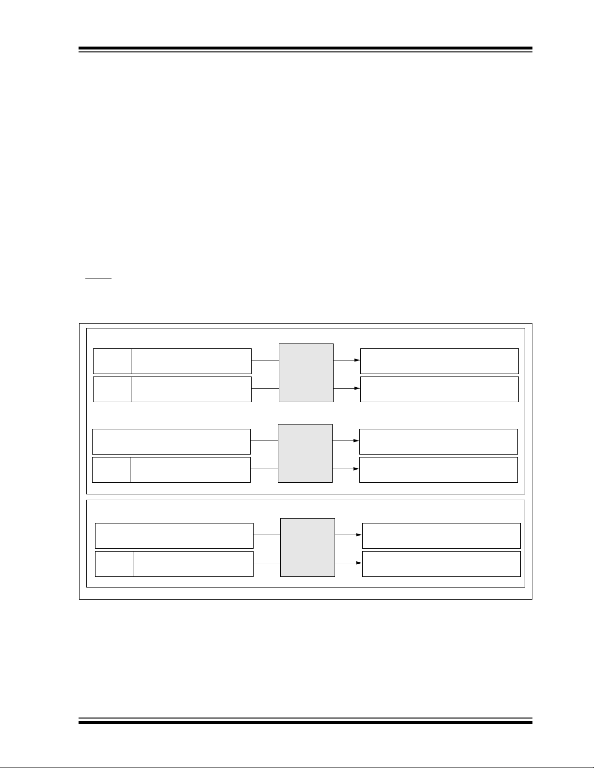
FIGURE 1-1: CREATION AND STORAGE OF CRYPT KEY DURING PRODUCTION
Production
Programmer
Manufacturer’s
Code
The 16-bit synchronization counter is the basis behind
the transmitted code word changing for each transmission; it increments each time a button is pressed. Due
to the code hoppin g algorith m’s complex ity, each increment of the synchronization value results in greater
than 50% of the bits changing in the transmitted code
word.
Figure 1-2 shows how the key values in EEPROM are
used in the encoder . O nce the encoder dete cts a button
press, it reads the button inputs and updates the synchronization counter. The synchronization co unter and
crypt key are input to the encryption algorithm and the
output is 32 bits of encrypted information. This data will
change with every button press, its value appearing
externally to ‘ran domly h op aroun d’, hence it is re ferred
to as the hopping portion of the code word. The 32-bit
hopping code is combined with the button information
and serial numb er to fo rm the code word transm itted to
the receiver. The code word format is explained in
greater detail in Section 8.2.
Transmitter
Serial Number
Key
Generation
Algorithm
HCS512
EEPROM Array
Serial Number
Crypt Key
Sync Counter
Crypt
Key
A receiver may use any type of controller as a decoder,
but it is typically a microcontroller with compatible firmware that allows the decoder to operate in conjunction
with an HCS512 based transmitter. Section 5.0
provides detail on integrating the HCS512 into a system.
A transmitter must first be ‘learned’ by the receiver
before its use is allowed in the system. Learning
includes calculating the transmitter’s appropriate crypt
key, decrypting the received hopping code and storing
the serial number, synchronization counter value and
crypt key in EEPROM.
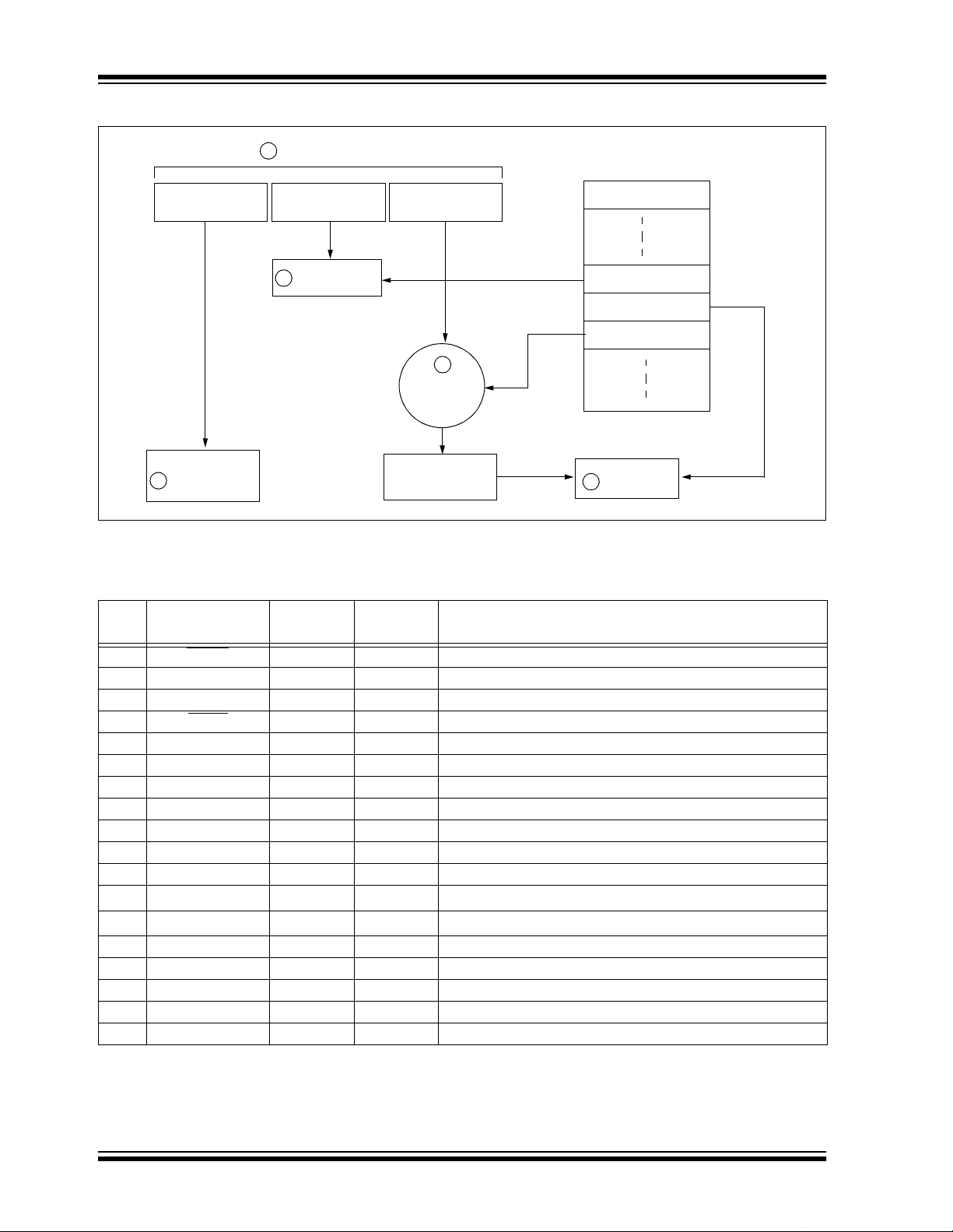
In normal operation, each received message of valid
format is evaluated. The serial number is used to determine if it is from a learned transmitter. If from a learned
transmitter, the message is decrypted and the synchronization counter is verified. Finally, the button status is
checked to see what operation is requested. Figure 1-3
shows the relationship between some of the values
stored by the receiver and the values received from
the transmitter.
.
.
.
FIGURE 1-2: BUILDING THE TRANSMITTED CODE WORD (ENCODER)
EEPROM Array
Crypt Key
Sync Counter
Serial Number
2002 Microchip Technology Inc. DS40151D-page 3
KEELOQ
Encryption
Algorithm
Button Press
Information
Serial Number
Transmitted Information
Encrypted Data
32 Bits
Page 4
HCS512
FIGURE 1-3: BASIC OPERATION OF RECEIVER (DECODER)
1
Received Information
Button Press
Information
Serial Number
32 Bits of
Encrypted Data
EEPROM Array
Manufacturer Code
Check for
2
Match
KEELOQ
Decryption
Algorithm
Perform Function
Indicated by
5
button press
NOTE: Circled numbers indicate the order of execution.
Decrypted
Synchronization
Counter
3
Serial Number
Sync Counte r
Crypt Key
Check for
4
Match
2.0 PIN ASSIGNMENT
PIN
1 LRNIN
2 LRNOUT O TTL Learn output - indicates learning
3NC — TTL Do not connect
4MCLR
5 Ground P — Ground connection
6S0 OTTL Switch 0
7S1 OTTL Switch 1
8S2 OTTL Switch 2
9S3 OTTL Switch 3
10 V
11 SLEEP I TTL Connect to RFIN to allow wake-up from SLEEP
12 CLK I/O
13 DATA I/O
14 V
15 OSCOUT (1MHZ) O TTL Oscillator out (test point)
16 OSC
17 NC — —
18 RFIN I TTL RF input from receiver
Note 1: P = power, I = in, O = out, and ST = Schmitt Trigger input.
Decoder
Function
LOW O TTL Battery low indication output
DD P — Power connection
IN (4MHz) I ST Oscillator in – recommended values 4.7 kΩ and 22 pF
2: Pin 12 and Pin 13 have a dual purpose. After RESET, these pins are used to determine if Programming
mode is selected in which case they are the clock and data lines. In normal operation, they are the clock
and data lines of the synchronous data output stream.
(1)
I/O
I TTL Learn input - initiates learning, 10K pull-up required on input
I ST Master clear input
Buffer
Type
TTL/ST
TTL/ST
(1)
(2)
(2)
Description
Clock in Programming mode and Synchronous mode
Data in Programming mode and Synchronous mode
DS40151D-page 4 2002 Microchip Technology Inc.
Page 5
HCS512
3.0 DESCRIPTION OF FUNCTIONS
3.1 Parallel Interface
The HCS512 activates the S3, S2, S1 & S0 outputs
when a new valid code is received. The outputs will be
activated for approxi mat ely 50 0 ms. I f a repeated code
is received during this time, the output extends for
approximately 500 ms.
3.2 Serial Interface
The decoder has a PWM/Synchronous interface connection to microcontrol lers with l imited I/O. An output
data stream is generated when a valid transmission is
received. The data stream consists of one START bit,
four function bits, one bit for battery status, one bit to
indicate a repeated transmission, two status bits, and
one STOP bit. (Table 3-1). The DA T A and CLK line s are
used to send a synchronous event message.
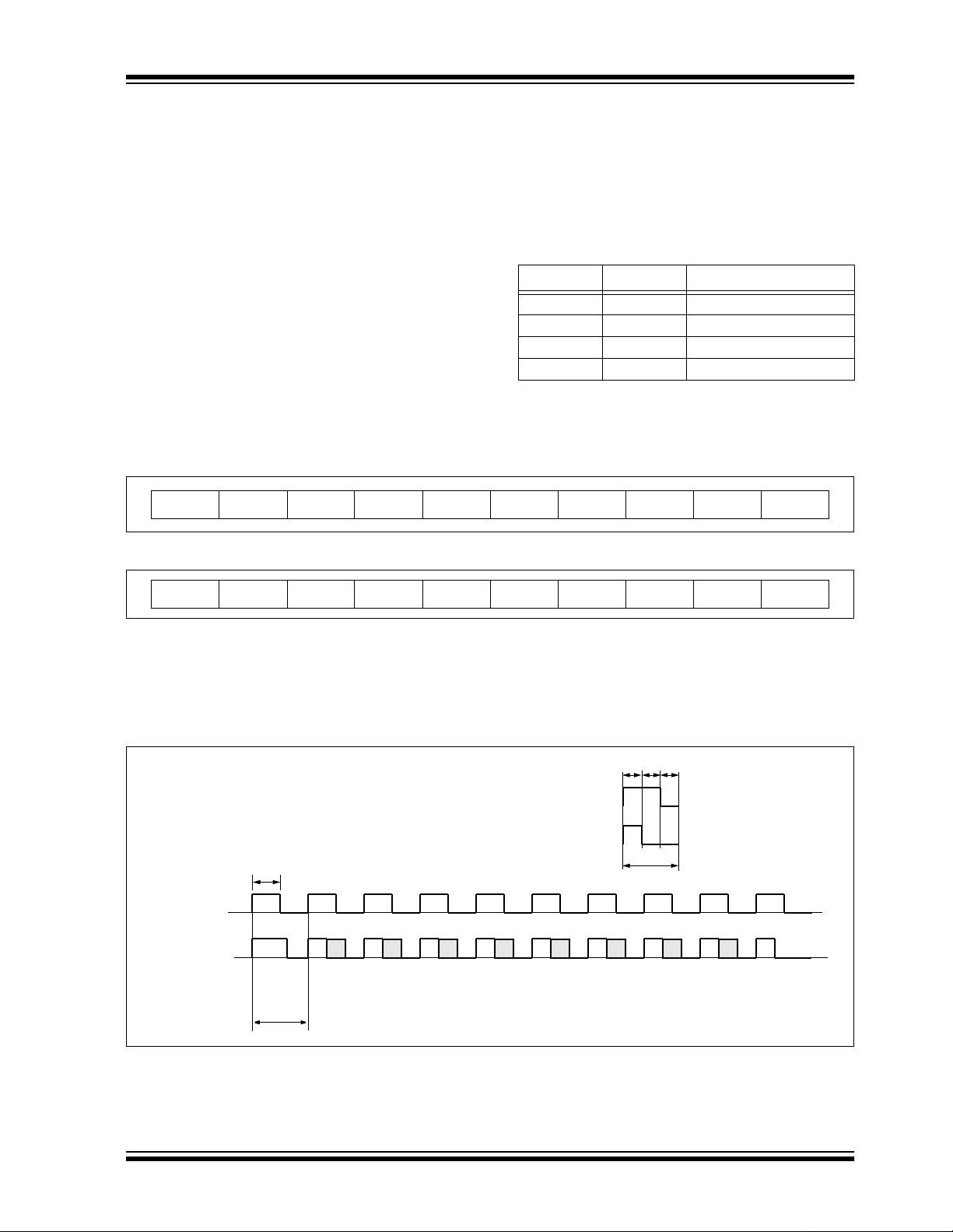
FIGURE 3-1: DATA OUTPUT FORMAT
STARTS3S2S1S0
FIGURE 3-2: STATUS MESSAGE FORMAT
A special statu s mess age is transmitted on the sec on d
pass of learn. Th is al lows th e cont rollin g mic rocont roller to determine if the learn w as successful (R esult = 1)
and if a previous transmitte r was overwritten (Overwri te
= 1). The status message is shown in Figure 3-2.
Table 3-1 show the values for TX1:0 and th e number of
transmitters learned.
TABLE 3-1: STATUS BITS
TX1 TX0 Number of Transmitters
00 One
01 Two
10 Three
11 Four
VLOW
TX1 TX0 STOPREPEAT
START0000
A 1-wire PWM or 2-wire synchronous interface can be used.
In 1-wire mode, the data is transmitted as a PWM signal with a basic pulse width of 400 µs.
In 2-wire mode, Synchronou s mode PWM bit s sta rt on the rising edg e of the clock, an d the bits must be sampl ed on the
falling edge. The START bit is a ‘1’ and the STOP bit is ‘0’.
FIGURE 3-2: PWM OUTPUT FORMAT
600 µs
CLK
DATA
S3START S2 S1 S0 VLOW RPT Reserved Reserved STOP
1200 µs
(1)
RESUL T
TX1 TX0 STOPOVRWR
1/31/31/3
LOGIC “1”
LOGIC “0”
1200 µs
Note: The Decoder output PWM format logic (“1” / “0”) is reversed with respe ct of the Encoder modulat ion format.
2002 Microchip Technology Inc. DS40151D-page 5
Page 6
HCS512
4.0 DECODER OPERATION
4.1 Learning a Transmitter to a
Receiver
Either the serial number-based learning method or the
seed-based learning method can be selected. The
learning method is s elected in t he config uration byte. In
order for a transmitter to be used with a decoder, the
transmitter must f irst be ‘learn ed’. When a transmitte r is
learned to a decoder, the decoder stores the crypt key,
a check value of the serial number and current synchronization value in EEPROM. The decoder must
keep track of these values for every transmitter that is
learned. The maxim um numbe r of trans mitters that can
be learned is four. The decoder must also contain the
Manufacturer’s Code in order to learn a transmitter.
The Manufacturer’s Code will typically be the same for
all decoders in a system.
The HCS512 has four memory slots. After an “erase
all” procedure, all the memory slots will be cleared.
Erase all is activated by taking LRNIN
mately 10 seconds . When a new transm itter is lea rned,
the decoder searches for an empty memory slot and
stores the transmitter’s informati on in that memory slo t.
When all memory slots are full, the decoder randomly
overwrites existing transmitters.
4.1.1 LEARNING PROCEDURE
Learning is activated by taking the LRNIN input low for
longer than 64 ms. Thi s inp ut req uire s an external pullup resistor.
To learn a new transmitter to the HCS512 decoder, the
following sequence is required:
1. Enter Learning mode by pulling LRNIN
longer than 64 ms. The LRNOUT output will go
high.
2. Activate the transmitter until the LRNOUT out-
put goes low indic ating re cepti on of a v alid code
(hopping message).
3. Activate the transmitter a second time until the
LRNOUT toggles for 4 seconds (in Secure
Learning mode, the seed transmission must be
transmitte d dur in g the s eco nd sta ge o f le arn by
activatin g the ap propria te butt ons on t he trans mitter).
If LRNIN
learn status indication, the indication will be terminated. Onc e a succe ssful l earning sequen ce
is detected, the indication can be terminated
allowing quick learning in a manufacturing
setup.
4. The transmitter is no w lea r ned in to t he d ec oder.
5. Repeat steps 1-4 to learn up to four tran smitters.
6. Learning will be terminated if two non-sequential
codes were received or if two acceptable codes
were not decoded within 30 seconds.
is taken low momentarily during the
low for approxi-
low for
The following checks are performed on the decoder to
determine if the transmission is valid during learn:
• The first code word is checked for bit integrit y.
• The second code word is c hec ke d f or b it i nte grit y.
• The hopping code is decrypted.
• If all the checks pass, the serial number and synchronization counters are stored in EEPROM
memory.
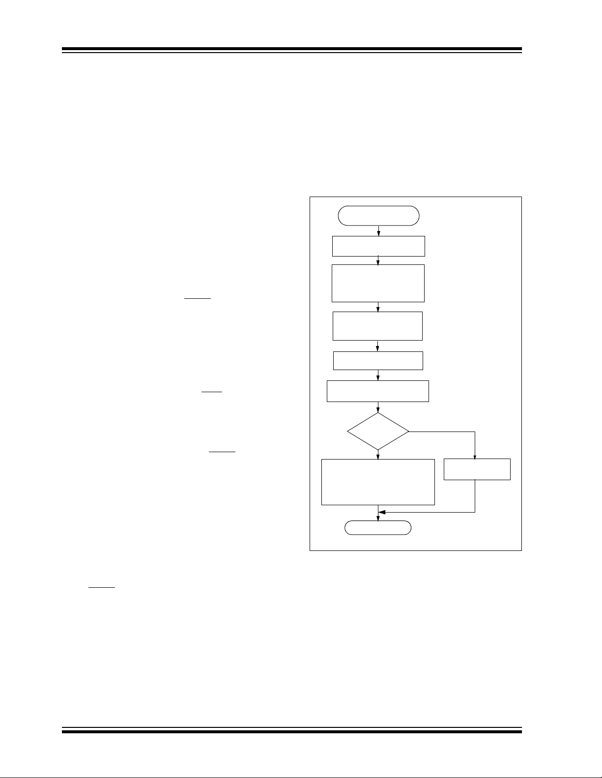
Figure 4-1 shows a flow chart of the learn sequence.
FIGURE 4-1: LEARN SEQUENCE
Enter Learn
Mode
Wait for Reception
of a Valid Code
Wait for Reception
of Second
Non-Repeated
V alid Code
Generate Key
from Serial Number
or Seed Value
Use Generated Key
to Decrypt
Compare Discrimination
Value with Serial Number
Equal
?
Yes
Learn successful. Store:
Serial number check value
Synchronization counter
crypt key
Exit
No
Learn
Unsuccessful
DS40151D-page 6 2002 Microchip Technology Inc.
Page 7
HCS512
4.2 Validation of Codes
The decoder waits for a transmission and checks the
serial number to determine if the transmitter has been
learned. If learned, the decoder decryp ts the en crypted
portion of t he t rans mis sio n us ing t he cr ypt k ey. It uses
the discrimination bits to determine if the decryption
was valid. If everything up to this point is valid, the
synchronization value is evaluated.
4.3 Validation Steps
Validation consists of the following steps:
• Search EEPROM to find the Serial Number
Check Value Match
• Decrypt the Hopping Code
• Compare the 10 bits of discrimination value with
the lower 10 bits of serial number
• Check if the synchronization counter falls within
the first synchronization window.
• Check if the synchronization counter falls within
the second synchronization window.
• If a valid transmission is found, update the synchronization coun ter , el se use the next t ransmi tter
block and repeat the tests.
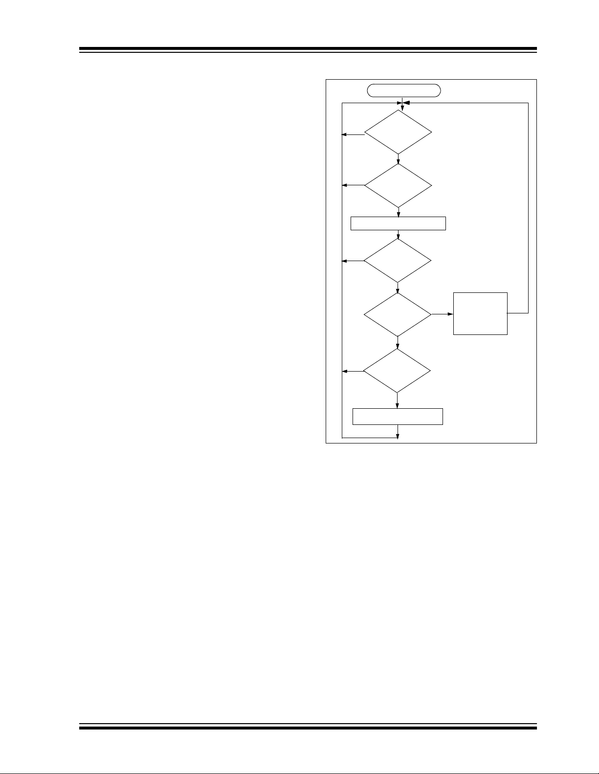
FIGURE 4-2: DECODER OPERATION
Start
No
Transmission
Received
?
Yes
No
Decrypt Transmission
No
No
Does
Ser # Check Val
Match
?
Yes
Is
Decryption
Valid
?
Yes
Is
Counter
Within 16
?
No
Is
Counter
Within 32K
?
Yes
Execute
Command
and
Update
Counter
Yes
Save Counter
in Temp Location
2002 Microchip Technology Inc. DS40151D-page 7
Page 8
HCS512
4.4 Synchronization with Decoder
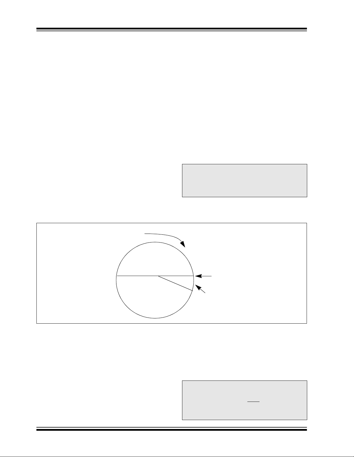
(Evaluating the Counter)
The KEELOQ technology patent scope includes a
sophisticated synchronization technique that does not
require the calculation and s torage of future codes. The
technique sec urely blocks inva lid transmission s while
providing transparent resynchronizat ion to t r ans mi tte rs
inadvertently activated away from the receiver.
Figure 4-3 shows a 3-partition, rotating synchronization
window. The size of each window is optional but the
technique is fundamental. Each time a transmission is
authenticated, the intended function is executed and
the transmission’s synchronization counter value is
stored in EEPROM. From the currently stored counter
value there is an initial "Single Operation" forward window of 16 codes. If the difference between a received
synchronization counter and the last stored counter is
within 16, the intended fun ction wi ll be ex ecuted on the
single button press and the new synchronization
counter will be st ored. Stori ng the new s y nch ron iz atio n
counter value ef fectively rot ates the entire synchronization window.
A "Double Operation" (resynchronization) window further exists from the Si ngle Ope ration wind ow up to 3 2K
codes forward of the currently stored counter value. It
is referred to as "Double Operation" because a transmission with synchronization counter value in this window will require an additional, sequential counter
transmissi on prior to execut ing the intended function.
Upon receiving the sequential transmission the
decoder executes the intended function and stores the
synchroniz ation co unter va lue. Th is resy nchroniz ation
occurs transparently to the user as it is human nature
to press the button a second t ime if the first was un successful.
The third window is a "Blocked Window" ranging from
the double operation window to the currently stored
synchroniz ation counter value. An y transmission with
synchronization counter value within this window will
be ignored. This window excludes previously used,
perhaps code-grabbed transmissions from accessing
the system.
Note: The synchronization method described in
this section is only a typic al implement ation
and because it is usually implemented in
firmware, it can be altered to fit the needs
of a particular system.
FIGURE 4-3: SYNCHRONIZATION WINDOW
Entire Window
rotates to eliminate
use of previously
used codes
Blocked
Window
(32K Codes)
Double Operation
(resynchronization)
Window
(32K Codes)
4.5 SLEEP Mode
The SLEEP mode of the HCS512 is used to reduce
current consumption when no RF input signal is
present. SLEEP mode will only be effective in systems
where the RF re ceiver is relat ively q uiet when no si gnal
is present. During SLEEP, the clock stops, thereby significantly reducing the operating current. SLEEP mode
is enabled by the SLEEP bit in the configuration byte.
The HCS512 will enter SLEEP mode when:
• The RF line is low
• After a function output is switched off
• Learn mode is terminated (time-out reached)
Stored
Synchronization
Counter Value
Single Operation
Window
(16 Codes)
The device will not enter SLEEP mode when:
• A function output is active
• Learn sequence active
• Device is in Programming mode
The device will wake-up from SLEEP when:
• The SLEEP input pin changes state
• The CLOCK line changes state
Note: During SLEEP mode the CLK line will
change from an output line to an input line
that can be used to wake-up the device.
Connect CLK to
to reliably enter the Learn mode whenever
SLEEP mode is active.
LRNIN via a 100K resistor
DS40151D-page 8 2002 Microchip Technology Inc.
Page 9

HCS512
5.0 INTEGRATING THE HCS512 INTO A SYSTEM
The HCS512 can act as a stand-alone decoder or be
interfaced to a microcontroller. Typical stand-alone
applications include garage door openers and electronic door locks. In stand-alone applications, the
HCS512 will handle learning, reception, decryption,
and validation of the received code; and generate the
appropriate output. For a garage door opener, the
HCS512 input will be conne cted t o an RF recei ver, and
the output, to a relay driver to connect a motor controller.
Typical systems where the HCS512 will be connected
to a microcontroller include vehicle and home security
systems. The HCS51 2 input wil l be connect ed to an RF
receiver and the function outputs to the microcontroller.
The HCS512 will hand le all the decod ing fun ctions an d
the microcontroller, all the system functi ons. T he Seria l
Output mode with a 1- or 2-wire interface can be used
if the microcontroller is I/O limited.
6.0 DECODER PROGRAMMING
The PG306001 production programmer will allow easy
setup and programming of the configuration byte and
the manufacturer’s code.
6.1 Configuration Byte
The configuration b yte is used to set sys tem c onfigu ration for the decoder. The LRN bits determine which
algorithm (Decrypt or XOR ) is used for th e key g eneration. SC_LRN determines whether normal learn (key
derived from serial number) or secure learn (key
derived from seed value) is used.
TABLE 6-1: CONFIGURATION BYTE
Bit Name Description
0 LRN0 Learn algorithm select
1 LRN1 Not used
2 SC_LRN Secure Learn enable (1 = enabled)
3 SLEEP SLEEP enable (1 = enabled)
4 RES1 Not used
5 RES2 Not used
6 RES3 Not used
7 RES4 Not used
TABLE 6-2: LEARN METHOD LRN0, LRN1
DEFINITIONS
LRN0 Description
0 Decrypt algorithm
1 XOR algorithm
2002 Microchip Technology Inc. DS40151D-page 9
Page 10

HCS512
6.2 Programming the Manufacturer’s
Code
The manufacturer’s code must be programmed into
EEPROM memory through the synchronous programming interface using the DA T A and CLK lines. Provi sion
must be made for connections to these pins if the
decoder is going to be programmed in circuit.
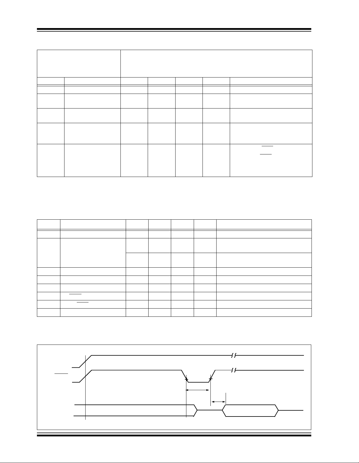
Programming mode is activated if the CLK is low for at
least 1 ms and then goes high within 64 ms after powerup, stays high for longer than 8 ms but not longer than
128 ms. After entering Programming mode the 64-bit
manufacturer’s code, 8-bit c onfigu rati on byte, and 8-bit
checksum is sent to the device using the synchronous
interface. After receiv ing the 80-bit message th e checksum is verified and the information is written to
EEPROM. If the programming operation was successful, the HCS512 will respond with an Acknowledge
pulse.
After programming the manufacturer’s code, the
HCS512 decoder will automatically activate an
Erase All function, removing all transmitters from the
system.
6.3 Download Format
The manufacturer’s code and configuration byte must
be downloaded Least Significant Byte, Least Significant bit first as shown in Table 6-3.
6.4 Checksum
The checksum is used by the HCS512 to check that the
data downloaded was correctly received before programming the dat a. The check sum is calcul ated so that
the 10 bytes added together (discarding the overflow
bits) is zero. The checksum can be calculated by adding the first 9 bytes of dat a togethe r and sub tracting th e
result from zero. Throughout the calculation the overflow is discarded.
Given a manufacturer’s code of 0123456789ABCDEF
checksum is calculated as shown in Figure 6-1. The
checksum is 3F16.
and a Configuration Word of 116, the
16
6.5 Test Transmitter
The HCS512 decoder will automatically add a test
transmitter each time an Erase All Function is done. A
test transmitter is defined as a transmitter with a serial
number of zero. After an Erase All, the test transmitter
will always work without l earning and will not c heck th e
synchronization counter of the transmitter. Learning of
any new transmitters will erase the test transmitter.
Note 1: A transmitter with a serial number o f ze ro
cannot be learned. Learn will fail after the
first transmission.
2: Always learn at least one transmitter aft er
an Erase All sequence. This ensures that
the test transmitter is erased.
TABLE 6-3: DOWNLOAD DATA
Byte 9 Byte 8 Byte 7 Byte 6 Byte 5 Byte 4 B yte 3 Byte 2 Byte 1 Byte 0
Check-
sum
Config
Man
Key_7
Man
Key_6
Man
Key_5
Man
Key_4
Man
Key_3
Byte 0, right-most bit downloaded first.
Man
Key_2
Man
Key_1
FIGURE 6-1: CHECKSUM CALCULATION
0116 + 2316 = 24
2416 + 4516 = 69
6916 + 6716 = D0
D016 + 8916 = 159
5916 + AB16 = 10416 (Carry is discarded)
+ CD16 = D116 (Carry is discarded)
04
16
+ EF16 = 1C0
D1
16
C016 + 116 = C116 (Carry is discarded)
- C116) + 116 = 3F
(FF
16
6
16
16
16
16
16
Man
Key_0
DS40151D-page 10 2002 Microchip Technology Inc.
Page 11

FIGURE 6-2: PROGRAMMING WAVEFORMS
MCLR
T
CKL
Bit1Bit0 Bit78 Bit79
CLK
(Clock)
DAT
(Data)
T
PS
T
PH1
Enter Program Mode
T
PH2
T
CKH
80-bit Data Package
T
ACK
Acknowledge
HCS512
T
ACKH
Ack
pulse
TABLE 6-4: PROGRAMMING TIMING REQUIREMENTS
Parameter Symbol Min. Max. Units
Program mode setup time TPS 1 64 ms
Hold time 1 TPH1 8 128 ms
Hold time 2 TPH2 0.05 320 ms
Clock High Time TCKH 0.05 32 0 ms
Clock Low Time TCKL 0.050 320 ms
Acknowledge Time TACK —80ms
Acknowledge duration TACKH 1 — ms
Note: FOSC equals 4 MHz.
2002 Microchip Technology Inc. DS40151D-page 11
Page 12
HCS512
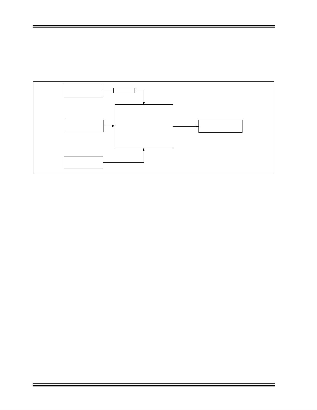
7.0 KEY GENERATION SCHEMES
The HCS512 decode r h as tw o k ey g ene rati on sc he me s. N orm al l earn ing u se s the tra ns mitter’s serial number to de riv e
two input seeds which are used as inputs to the key generation algorithm. Secure learning uses the seed transmission
to derive the two input seeds. Two key generation algorithms are available to convert the inputs seeds to secret keys.
The appropriate scheme is selected in the Configuration Word.
FIGURE 7-1:
Serial
Number
Manufacturer’s
Key
Seed
Patched
Key Generation
Algorithms
------------------Decrypt
XOR
Encoder
Key
7.1 Normal Learning (Serial Number Derived)
The two input seeds are composed from the serial number in two ways, depending on the encoder type. The encoder
type is determine d from th e numb er of bit s in the inc oming tran smis sion. SourceH is used to calc ulate the upp er 32 bits
of the crypt key, and SourceL, for the lower 32 bits.
For 28-bit serial number encoders (66 / 67-bit transmissions):
SourceH = 6H + 28 bit Serial Number
SourceL = 2H + 28 bit Serial Number
7.2 Secure Learning (Seed Derived)
The two input seeds are c om pos ed fr om the s eed val ue th at is tran sm itted during secure lear ni ng. Th e lo w er 32 b it s of
the seed transmission is used to compose the lower seed, and the upper 32 bits, for the upper seed. The upper 4 bits
(function code) are set to zero.
For 32-bit seed encoders:
SourceH = Serial Number
SourceL = Seed
32 bits
Lower 28 bits
(with upper 4 bits always zero)
For 48-bit seed encoders:
SourceH = Seed
SourceL = Seed
Upper 16 bits
Lower 32 bits
+ Serial Number
Upper 16 bits
(with upper 4 bits always zero) << 16
For 60-bit seed encoders:
SourceH = Seed
SourceL = Seed
DS40151D-page 12 2002 Microchip Technology Inc.
Upper 28 bits
Lower 32 bits
(with upper 4 bits always zero)
Page 13
HCS512
7.3 Key Generation Algorithms
There are two key generation algorithms implemented in the HCS512 decoder. The KEELOQ decryption algorithm provides a higher level of s ecurity th an the XOR alg orithm. Section 6.1 describes the se lectio n of the algo rithms in th e configuration byte.
7.3.1 KEELOQ DECRYPT ALGORITHM
This algorithm uses the KEELOQ decryption algorithm and the manufacturer’s code to derive the crypt key as follows:
Key
Upper 32 bits
Key
Lower 32 bits
7.3.2 XOR WITH THE MANUFACTURER’S CODE
The two 32-bits seeds are XOR with the manufacturer’s code to form the 64 bit crypt key.
Key
Upper 32 bits
Key
Lower 32 bits
After programming the manufacturer’s code, the HCS512 decoder will automatically activate an Erase All function,
removing all transmitters from the system.
If LRNIN
learning sequence is detected, the indication can be terminated, allowing quick learning in a manufacturing setup.
FIGURE 7-2: HCS512 KEY GENERATION
= Decrypt (SourceH)
= Decrypt (SourceL)
= SourceH XOR Manufacturers Code
= SourceL XOR Manufacturers Code
64 Bit Manufacturers Code
64 Bit Manufacturers Code
Upper 32 bits
Lower 32 bits
is taken low moment arily du ring the learn st atus indica tion, the indica tion will be term inated. Once a su ccessful
Normal Learn (SC_LRN = 0)
Padding
2
Padding
6
Padding
0000b
Padding
0000b
28-bit Serial Number
28-bit Serial Number
Secure Learn (SC_LRN = 1)
LS 32 bits of Seed Transmission
MS 28 bits of Seed Transmission
Secure Learn XOR (SC_LRN = 1)
LS 32 bits of Seed Transmission
MS 28 bits of Seed Transmission
LRN0 = 0
KEELOQ
Decryption
Algorithm
LRN0 = 0
KEELOQ
Decryption
Algorithm
LRN0 = 1
XOR
LS 32 bits of crypt key
MS 32 bits of crypt key
LS 32 bits of crypt key
MS 32 bits of crypt key
LS 32 bits of crypt key
MS 32 bits of crypt key
2002 Microchip Technology Inc. DS40151D-page 13
Page 14

HCS512
8.0 KEELOQ ENCODERS
8.1 Transmission Format (PWM)
The KEELOQ encoder transmission is made up of sev-
eral parts (Figure 8-1). Each transmission begins with
a preamble and a header, followed by the encrypted
and then the fixed data. The actual data is 66/69 bits
which consists of 32 bits of encrypted data and 34/37
bits of non-enc rypted data. Each transmis sion is followed by a guard period before another transmission
can begin. The encrypted portion provides up to four
billion changing code combinations and includes the
button status bits (based on which buttons were activated) along with the synchronization counter value
and some discrimination bits. The non-encrypted portion is comprised of the status bits, the function bits,
FIGURE 8-1: TRANSMISSION FORMAT (PWM)
and the 28-bit serial number. The encrypted and nonencrypted combined sections increase the number of
combinations to 7.38 x 10
19
.
8.2 Code Word Organization
The HCSXXX encoder transmit s a 66/69- bit co de word
when a button is pressed. The 66/69-bit word is constructed from an encryption portion and a nonencrypted code portion (Figure 8-2).
The Encrypted Data is gen erated from four button bit s,
two overflow counter bits, ten discrimination bits, and
the 16-bit synchronization value.
The Non-encrypted Data is made up from 2 status
bits, 4 function bits, and the 28/32-bit serial number.
TETET
LOGIC "0"
LOGIC "1"
E
T
BP
Preamble
50%
10xTE
Header
FIGURE 8-2: CODE WORD ORGANIZATION
34 bits of Fixe d Portion 32 bits of Encrypted Portion
MSb
MSb
Repeat
(1-bit)
Repeat
(1-bit)
VLOW
(1-bit)
Button
Status
S2 S1 S0 S3
V
LOW
(1-bit)
Button
Status
1 1 1 1
SEED replaces Encrypted Portion when all button inputs are activated at the same time.
Serial Number
(28 bits)
Serial Number
(28 bits)
Encrypted
Portion
Button
Status
S2 S1 S0 S3
Portion
OVR
(2 bits)
Fixed Code
DISC
(10 bits)
SEED
(32 bits)
Guard
Time
Sync Counter
(16 bits)
66 Data bits
Transmitted
LSb first.
LSb
LSb
DS40151D-page 14 2002 Microchip Technology Inc.
Page 15

HCS512
9.0 ELECTRICAL CHARACTERISTICS FOR HCS512
Absolute Maximum Ratings †
Ambient temperature under bias.............................................................................................................-55°C to +125°C
Storage temperature...............................................................................................................................-65°C to +150°C
Voltage on any pin with respect to
Voltage on
VDD with respect to Vss...................................... ...... ...... ..... ...... ..... ........................................ ..........0 to +7.5V
Total power dissipation (Note 1) ..........................................................................................................................800 mW
Maximum current out of
Maximum current into
Input clamp current, Iik (
VSS pin.............................................................................................................................150 mA
VDD pin................................................................................................................................100 mA
VI < 0 or VI > VDD).................................................. ..... ...... ...... ....................................... ..± 20 mA
Output clamp current, IOK (V
Maximum output current sunk by any I/O pin..........................................................................................................25 mA
Maximum output current sourced by any I/O pin....................................................................................................20 mA
Note: Power dissipation is calculated as follows: Pdis = V
† NOTICE: Stresses above those listed under “Absolute Maximum Ratings” may cause permanent damage to the
device. This is a stress rating only and functional operation of the device at those or any other conditions above
those indicated in the ope ration listi ngs of this speci fication is not implied. Exposure to maxim um rating co nditions for
extended periods may affect device reliability.
VSS (except VDD) ............................................................................ -0.6V to VDD +0.6V
O < 0 or VO >VDD) ........................................................................... ...... ...................± 20 mA
DD x {IDD - ∑ IOH} + ∑ {(VDD–VOH) x IOH} + ∑(VOl x IOL)
2002 Microchip Technology Inc. DS40151D-page 15
Page 16
HCS512
TABLE 9-1: DC CHARACTERISTICS
Standard Operating Conditions (unless otherwise stated)
Operating temperature
Commercial (C): 0°C ≤ TA ≤ +70°C for commercial
Industrial (I): -40°C ≤ T
Symbol Characteristic Min Typ
DD Supply Voltage 4.0 —6.0V
V
VPOR VDD start voltage to
—VSS —V
(†)
ensure RESET
S
VDD VDD rise rate to
0.05* — — V/ms
ensure RESET
DD Supply Current —
I
—
1.8
7.3
15
VIL Input Low Voltage VSS —0.16 VDD Vexcept MCLR = 0.2 VDD
VIH Input High Voltage 0.48 VDD —VDD Vexcept MCLR = 0.85 VDD
VOL Output Low Voltage — — 0.6 V IOL = 8.5 mA, VDD = 4.5V
VOH Output High Voltage VDD-0.7 — — V IOH = -3.0 mA, VDD = 4.5V
† Data in “Typ” column is at 5.0V, 25°C unless otherwise stated. These parameters are for design guidance only
and are not tested.
* These parameters are characterized but not tested.
Note: Negative current is defined as coming out of the pin.
A ≤ +85°C for industrial
Max U nits Conditions
4.5
10
32
mA
mA
µA
FOSC = 4 MHz, VDD = 5.5V
(During EEPROM programming)
In SLEEP mode
TABLE 9-2: AC CHARACTERISTICS
Symbol Characteristic Min Typ Max Units Conditions
OSC Oscillator frequency 2.7 4 6.21 MHz REXT = 10K, CEXT = 10 pF
F
65 — 1080 µs 4.5V < VDD < 5.5V
E
T
PWM elemental
pulse width
130 — 1080 µs 3V < V
Oscillator components tolerance < 6%.
DD < 6V
Oscillator components tolerance <10%
T
OD Output delay 70 90 115 ms
TA Output activation time 322 500 740 ms
RPT REPEAT activation time 32 50 74 ms
T
TLRN LRNIN activation time 21 32 — ms
TMCLR MCLR low time 150 — — ns
OV Time output valid — 150 222 ms
T
* These parameters are characterized but not tested.
FIGURE 9-1: RESET WATCHDOG TIMER, OSCILLATOR START-UP TIMER AND POWER-UP
TIME R TIMI NG
VDD
MCLR
TMCLR
TOV
I/O Pins
DS40151D-page 16 2002 Microchip Technology Inc.
Page 17

2002 Microchip Technology Inc. DS40151D-page 17
RFIN
S[3,2,1,0]
1 Code Word 50 ms
TOD
FIGURE 9-2: OUTPUT ACTIVATION
Note 1
TA
VLOW
TA
LRNOUT
0s 1s 2s 3s 4s 5s
Note 2
Note 1: Output is activated as long as code is received.
2: Output is activated if battery low (
VLOW) is detected.
HCS512
Page 18
DS40151D-page 18 2002 Microchip Technology Inc.
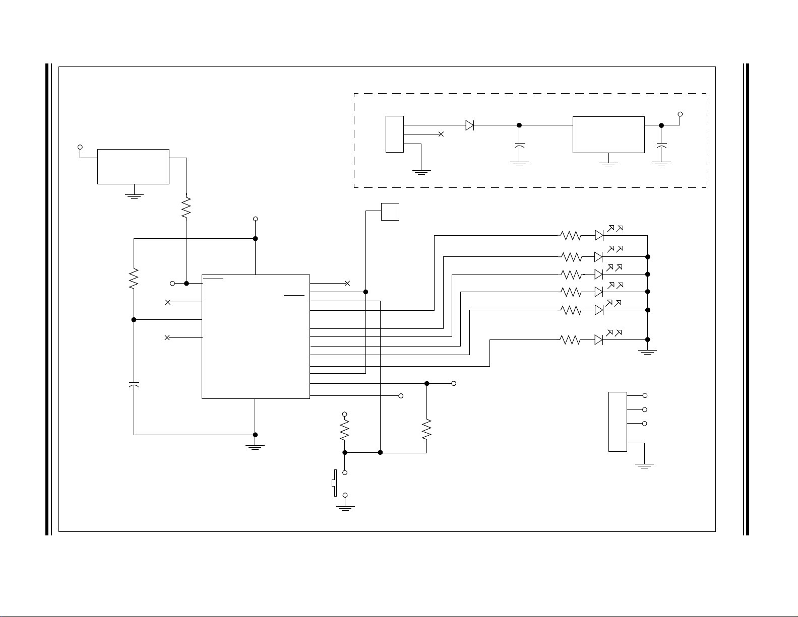
FIGURE 9-3: TYPICAL DECODER APPLICATION CIRCUIT
HCS512
MCP100-450
V
DD
LOW VOLTAGE DETECTOR—DO NOT OMIT
G
VI
VO
N
D
10K
P2
4.7K
4
MCLR
3
NC
16
OSC
15
OSCOUT
IN
22 pF
HCS512
VDD
V
G
VDD
100 µF
12V
GND
LM7805
1
2
3
1N4004/7
100 µF
VI
VO
G
N
D
POWER SUPPLY
RECEIVE DATA INPUT
1
1K
1K
14
17
NC
18
D
D
N
D
5
RFIN
LRNIN
LRNOUT
S0
S1
S2
S3
VLOW
SLEEP
CLK
DAT
1
2
6
7
8
9
10
11
12
13
DD
10K
P4
100K
V
P3
1K
1K
1K
1K
DATA
CLOCK
RESET
LRNOUT
S0
S1
S2
S3
VLOW
P4
P3
P2
GND P1
LEARN
BUTTON
In-Circuit
Programming Pads
Page 19

10.0 PACKAGING INFORMATION
10.1 Package Marking Information
18-Lead PDI P (300 mil) Example
HCS512
XXXXXXXXXXXXXXXXX
XXXXXXXXXXXXXXXXX
YYWWNNN
18-Lead SOIC (300 mil) Example
XXXXXXXXXXXX
XXXXXXXXXXXX
XXXXXXXXXXXX
YYWWNNN
Legend: XX...X Customer specific information*
Y Year code (last digit of calendar year)
YY Year code (last 2 digits of calendar year)
WW Week code (week of January 1 is week ‘01’)
NNN Alphanumeric traceability code
HCS512
HCS512
/SO
0110017
01 10 017
Note: In the event the full Microchip part number can not be ma rked on one line, it will
be carried over to the next l ine thus lim it ing t he nu mb er of av ai lab le cha r ac ters
for customer specific information.
* Standard PICmicro device marking consists of Microchip part number, year code, week code, and
traceability code. For PICmicro device marking beyond this, certain price adders apply. Please check
with your Microchip Sales Office. For QTP devices, any special marking adders are included in QTP
price.
2002 Microchip Technology Inc. DS40151D-page 19
Page 20

HCS512
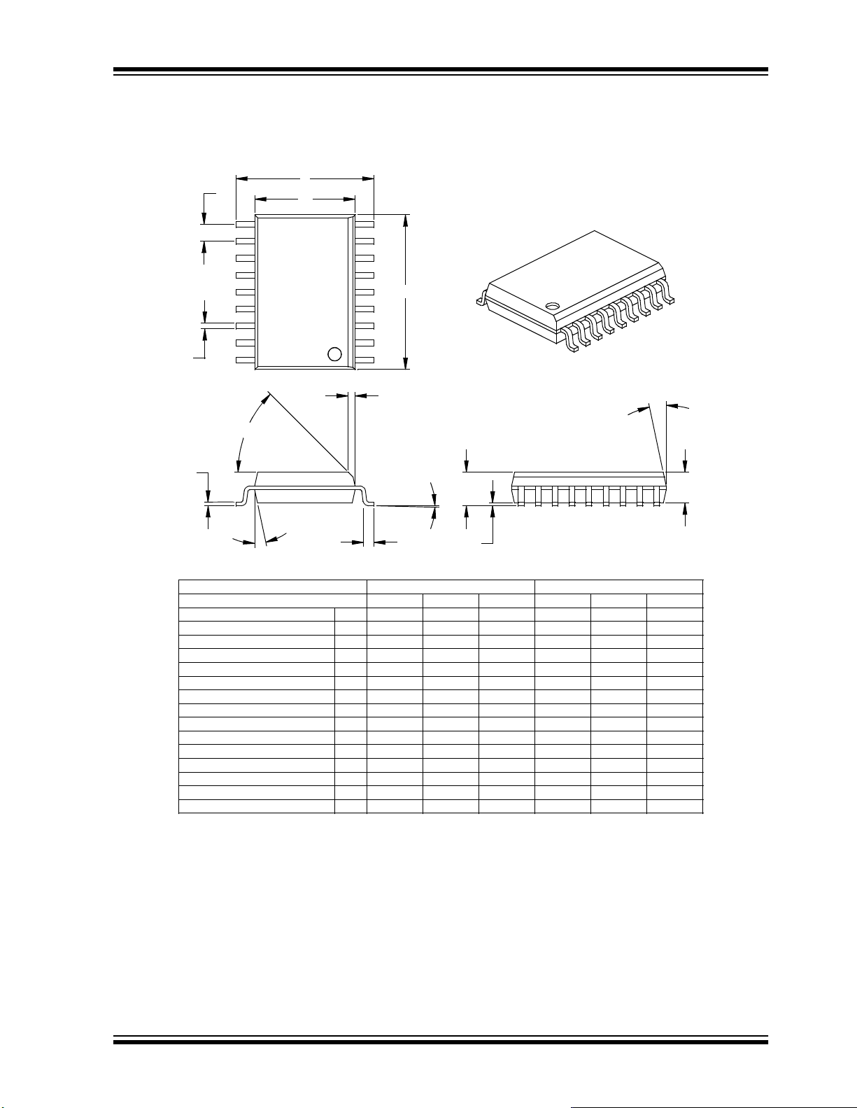
10.2 Package Details
18-Lead Plastic Dual In-line (P) – 300 mil (PDIP)
E1
D
2
n
1
α
E
A
c
A1
β
eB
Number of Pins
Pitch
Lead Thickne ss
Mold Draft Angle Top
Mold Draft Angle Bottom
* Controlling Parameter
§ Significant Characteristic
Notes:
Dimensions D and E1 do not include mold flash or protrusions. Mold flash or protrusions shall not exceed
.010” (0.254mm) per side.
JEDEC Equivalent: MS-001
Drawing No. C04-007
n
p
c
α
β
B1
B
0.38.015A1Base to Seating Plane
p
MILLIMETERSINCHES*Units
2.54.100
A2
L
MAXNOMMINMAXNOMMINDimension Limits
1818
4.323.943.56.170.155.140ATop to Seating Plane
3.683.302.92.145.130.115A2Molded Package Thickness
8.267.947.62.325.313.300EShoulder to Shoulder Width
6.606.356.10.260.250.240E1Molded Package Width
22.9922.8022.61.905.898.890DOverall Length
3.433.303.18.135.130.125LTip to Seating Plane
0.380.290.20.015.012.008
1.781.461.14.070.058.045B1Upper Lead Width
0.560.460.36.022.018.014BLower Lead Width
10.929.407.87.430.370.310eBOverall Row Spacing §
1510515105
1510515105
DS40151D-page 20 2002 Microchip Technology Inc.
Page 21
18-Lead Plastic Small Outline (SO) – Wide, 300 mil (SOIC)
HCS512
p
B
n
°
45
c
β
E1
E
D
2
1
h
A
φ
L
A1
α
A2
MILLIMETERSINCHES*Units
A2
n
p
φ
c
α
β
048048
1.27.050
Number of Pins
Pitch
Molded Package Thickness
Foot Angle
Lead Thickne ss
Mold Draft Angle Top
Mold Draft Angle Bottom
* Controlling Parameter
§ Significant Characteristic
Notes:
Dimensions D and E1 do not include mold flash or protrusions. Mold flash or protrusions shall not exceed
.010” (0.254mm) per side.
JEDEC Equivalent: MS-013
Drawing No. C04-051
MAXNOMMINMAXNOMMINDimension Limits
1818
2.642.502.36.104.099.093AOverall Height
2.392.312.24.094.091.088
0.300.200.10.012.008.004A1Standoff §
10.6710.3410.01.420.407.394EOverall Width
7.597.497.39.299.295.291E1Molded Package Width
11.7311.5311.33.462.454.446DOverall Length
0.740.500.25.029.020.010hChamfer Distance
1.270.840.41.050.033.016LFoot Length
0.300.270.23.012.011.009
0.510.420.36.020.017.014BLead Width
1512015120
1512015120
2002 Microchip Technology Inc. DS40151D-page 21
Page 22

HCS512
ON-LINE SUPPORT
Microchip provides on-line support on the Microchip
World Wide Web (WWW) site.
The web site is used b y Micr ochip as a means to mak e
files and information easily available to customers. To
view the site, the use r must hav e access to the Intern et
and a web browser, such as Netscape or Microsoft
Explorer. Files are also available for FTP download
from our FTP site.
Connecting to the Microchip Internet Web Site
The Microchip web site is available by using your
favorite Internet browser to attach to:
www.microchip.com
The file transfer site is available by using an FTP service to connect to:
ftp://ftp.microchip.com
The web site and file transfer site provide a variety of
services. Users may download files for the latest
Development Tools, Data Sheets, Application Notes,
User’s Guides, Articles and Sample Programs. A variety of Micr ochip specific bu siness informati on is also
available, including listings of Microchip sales offices,
distributors and factory representatives. Other data
available for consideration is:
• Latest Microchip Press Releases
• Technical Support Section with Frequently Asked
Questions
• Design Tips
• Device Errata
• Job Postings
• Microchip Consultant Program Member Listing
• Links to other useful web sites related to
Microchip Products
• Conferences for products , Development System s,
technical information and more
Listing of seminars and events
Systems Information and Upgrade Hot Line
The Systems Information and Upgrade Line provides
system users a listing of the latest versions of all of
Microchip's development systems software products.
Plus, this line provides information on how customers
can receive any currently available upgrade kits.The
Hot Line Numbers are:
1-800-755-2345 for U.S. and most of Canada, and
1-480-792-7302 for the rest of the world.
DS40151D-page 22 2002 Microchip Technology Inc.
Page 23

HCS512
READER RESPONSE
It is our intentio n t o provide you with the bes t doc um entation possible to en sure successful use of y our Microchip product. If you wish to pro vide your comm ents on org aniza tion, c larity, subject matter, and ways in which our doc umenta tion
can better serve you, please FAX your comments to the Technical Publications Manager at (480) 792-4150.
Please list the following information, and use this outline to provide us with your comments about this Data Sheet.
To:
RE: Reader Response
From:
Application (optional):
Would you like a reply? Y N
Device:
Questions:
1. What are the best features of this document?
2. How does this document meet your hardware and software development needs?
3. Do you find the organization of this data sheet easy to follow? If not, why?
Technical Publications Manager
Name
Company
Address
City / State / ZIP / Country
Telephone: (_______) _________ - _________
HCS512
Literature Number:
Total Pages Se nt
FAX: (______) _________ - _________
DS40151D
4. What additions to the data sheet do you think would enhance the structure and subject?
5. What deletions from the data sheet could be made without affecting the ov erall usefulness?
6. Is there any incorrect or misleading information (what and where)?
7. How would you improve this document?
8. How would you improve our software, systems, and silicon products?
2002 Microchip Technology Inc. DS40151D-page 23
Page 24

HCS512
HCS512 PRODUCT IDENTIFICATION SYSTEM
To order or obtain information, e.g., on pricing or delivery, refer to the factory or the listed sales office.
HCS512 — /P
Package:
P = Plastic DIP (300 mil Body), 18-lead
SO = Plastic SOIC (300 mil Body), 18-lead
Temperature
Range:
Device:
Blank = 0°C to +70°C
I =-40°C to +85°C
HCS512 Code Hopping Decoder
HCS512T Code Hopping Decoder (Tape and Reel)
Sales and Support
Data Sheets
Products supported by a preliminary Data Sheet may have an errata sheet describing minor operational differences and recommended workarounds. To determine if an errata sheet exists for a particular device, please contact one of the following:
1. Your local Microchip sales office
2. The Microchip Corporate Literature Center U.S. FAX: (480) 792-7277
3. The Microchip Worldwide Site (www.microchip.com)
Please specify which device, revision of silicon and Data Sheet (include Literature #) you are using.
New Customer Notification System
Register on our web site (www.microchip.com/cn) to receive the most current information on our products.
DS40151D-page 24 2002 Microchip Technology Inc.
Page 25

Microchip’s Secure Data Products are covered by some or all of the following patents:
Code hopping encoder patents issued in Europe, U.S.A., and R.S.A. — U.S.A.: 5,517,187; Europe: 0459781; R.S.A.: ZA93/4726
Secure learning patents issued in the U.S.A. and R.S.A. — U.S.A.: 5,686,904; R.S.A.: 95/5429
Information contained in this publication regarding device
applications and the like is intended through suggestion only
and may be superseded by updates. It is your responsibility to
ensure that your application meets with your specifications.
No representation or warranty is given and no liability is
assumed by Microchip Technology Incorporated with respect
to the accuracy or use of such information, or infringement of
patents or other intellectual property rights arising from such
use or otherwise. Use of Microchip’s products as critical components in life support systems is not authorized except with
express written approval by Microchip. No licenses are conveyed, implicitly or otherwise, under any intellectual property
rights.
Trademarks
The Microchip name and logo, the Microchip logo, FilterLab,
K
EELOQ, MPLAB, PIC, PICmicro, PICMASTER, PICSTART,
PRO MATE, SEEVAL and The Embedded Control Solutions
Company are registered trademarks of Microchip Technology
Incorporated in the U.S.A. and other countries.
dsPIC, ECONOMONITOR, FanSense, FlexROM, fuzzyLAB,
In-Circuit Serial Programming, ICSP, ICEPIC, microID,
microPort, Migratable Memory, MPASM, MPLIB, MPLINK,
MPSIM, MXDEV, PICC, PICDEM, PICDEM.net, rfPIC, Select
Mode and Total Endurance are trademarks of Microchip
Technology Incorporated in the U.S . A.
Serialized Quick Turn Programming (SQTP) is a service mark
of Microchip Technology Incorporated in the U.S.A.
All other trademarks mentioned herein are property of their
respective companies.
© 2002, Microchip Technology Incorporated, Printed in the
U.S.A., All Rights Reserved.
Printed on recycled paper.
Microchip received QS-9000 quality system
certification for its worldwid e head qu art ers,
design and wafer fabrication facilities in
Chandler and Tempe, Arizona in July 1999. The
Company’s quality system processes and
procedures are QS-9000 compliant for its
PICmicro
devices, Serial EEPROMs and microperipheral
products. In addition, Microchip’s quality
system for the design and manufacture of
development systems is ISO 9001 certified.
®
8-bit MCUs, KEELOQ
®
code hoppin g
2002 Microchip Technology Inc. DS40151D - page 25
Page 26

WORLDWIDE SALES AND SERVICE
AMERICAS
Corporate Office
2355 West Chandler Blvd.
Chandler, AZ 85224-6199
Tel: 480-792-7200 Fax: 480-792-7277
Technical Support: 480-792-7627
Web Address: http://www.microchip.com
Rocky Mountain
2355 West Chandler Blvd.
Chandler, AZ 85224-6199
Tel: 480-792-7966 Fax: 480-792-7456
Atlanta
500 Sugar Mill Road, Suite 200B
Atlanta, GA 30350
Tel: 770-640-0034 Fax: 770-640 -03 07
Boston
2 Lan Drive, Suite 120
Westford, MA 01886
Tel: 978-692-3848 Fax: 978-692 -38 21
Chicago
333 Pierce Road, Suite 180
Itasca, IL 60143
Tel: 630-285-0071 Fax: 630-285-0075
Dallas
4570 Westgrove Drive, Suite 160
Addison, TX 75001
Tel: 972-818-7423 Fax: 972-818 -29 24
Detroit
Tri-Atria Office Building
32255 Northwestern Highway, Suite 190
Farmington Hills, MI 48334
Tel: 248-538-2250 Fax: 248-538-2260
Kokomo
2767 S. Albright Road
Kokomo, Indiana 46902
Tel: 765-864-8360 Fax: 765-864-8387
Los Angeles
18201 Von Karman, Suite 1090
Irvine, CA 92612
Tel: 949-263-1888 Fax: 949-263 -13 38
New York
150 Motor Parkway, Suite 202
Hauppauge, NY 11788
Tel: 631-273-5305 Fax: 631-273 -53 35
San Jose
Microchip Technology Inc.
2107 North First Street, Suite 590
San Jose, CA 95131
Tel: 408-436-7950 Fax: 408-436 -79 55
Toronto
6285 Northam Drive, Suite 108
Mississauga, Ontario L4V 1X5, Canada
Tel: 905-673-0699 Fax: 905-673-6509
ASIA/PACIFIC
Australia
Microchip Technology Australia Pty Ltd
Suite 22, 41 Rawson Street
Epping 2121, NSW
Australia
Tel: 61-2-9868-6733 Fax: 61-2-9868-6755
China - Beijing
Microchip Technology Consulting (Shanghai)
Co., Ltd., Beijing Liaison Office
Unit 915
Bei Hai Wan Tai Bldg.
No. 6 Chaoyangmen Beidajie
Beijing, 100027, No. China
Tel: 86-10-85282100 Fax: 86-10-85282104
China - Chengdu
Microchip Technology Consulting (Shanghai)
Co., Ltd., Chengdu Liaison Office
Rm. 2401, 24th Floor,
Ming Xing Financial Tower
No. 88 TIDU Street
Chengdu 610016, China
Tel: 86-28-6766200 Fax: 86-28-6766599
China - Fuzhou
Microchip Technology Consulting (Shanghai)
Co., Ltd., Fuzhou Liaison Of fice
Unit 28F, World Trade Plaza
No. 71 Wusi Road
Fuzhou 350001, China
Tel: 86-591-7503506 Fax: 86-591-7503521
China - Shanghai
Microchip Technology Consulting (Shanghai)
Co., Ltd.
Room 701, Bldg. B
Far East International Plaza
No. 317 Xian Xia Road
Shanghai, 200051
Tel: 86-21-6275-5700 Fax: 86-21-6275-5060
China - Shenzhen
Microchip Technology Consulting (Shanghai)
Co., Ltd., Shenzhen Liaison Office
Rm. 1315, 13/F, Shenzhen Kerry Centre,
Renminnan Lu
Shenzhen 518001, China
Tel: 86-755-2350361 Fax: 86-755-2366086
Hong Kong
Microchip Technology Hongkong Ltd.
Unit 901-6, Tower 2, Metroplaza
223 Hing Fong Road
Kwai Fong, N.T., Hong Kong
Tel: 852-2401-1200 Fax: 852-2401-3431
India
Microchip Technology Inc.
India Liaison Office
Divyasree Chambers
1 Floor, Wing A (A3/A4)
No. 11, O’Shaugnessey Road
Bangalore, 560 025, India
Tel: 91-80-2290061 Fax: 91-80-2290062
Japan
Microchip Technology Japan K.K.
Benex S-1 6F
3-18-20, Shinyokohama
Kohoku-Ku, Yokohama- shi
Kanagawa, 222-0033, Japan
Tel: 81-45-471- 6166 Fax: 81-45-471-6122
Korea
Microchip Technology Korea
168-1, Youngbo Bldg. 3 Floor
Samsung-Dong, Kangnam-Ku
Seoul, Korea 135-882
Tel: 82-2-554-7200 Fax: 82-2-558-5934
Singapore
Microchip Technology Singapore Pte Ltd.
200 Middle Road
#07-02 Prime Centre
Singapore, 188980
Tel: 65-334- 8870 Fax: 65-334-8850
Taiwan
Microchip Technology Taiwan
11F-3, No. 207
Tung Hua North Road
Taipei, 105, Taiwan
Tel: 886-2-2717-7175 Fax: 886-2-2545-0139
EUROPE
Denmark
Microchip Technology Nordic ApS
Regus Business Centre
Lautrup hoj 1-3
Ballerup DK-2750 Denmark
Tel: 45 4420 9895 Fax: 45 4420 9910
France
Microchip Technology SARL
Parc d’Activite du Moulin de Massy
43 Rue du Saule Trapu
Batiment A - ler Etage
91300 Massy, France
Tel: 33-1-69-53-63-20 Fax: 33-1-69-30-90-79
Germany
Microchip Technology GmbH
Gustav-Heinemann Ring 125
D-81739 Munich, Germany
Tel: 49-89-627-144 0 Fax: 49-89-627-144-44
Italy
Microchip Technology SRL
Centro Direzionale Colleoni
Palazzo Taurus 1 V. Le Colleoni 1
20041 Agrate Brianza
Milan, Italy
Tel: 39-039-65791-1 Fax: 39-039-6899883
United Kingdom
Arizona Microchip Technology Ltd.
505 Eskdale Road
Winnersh Triangle
Wokingham
Berkshire, England RG41 5TU
Tel: 44 118 921 5869 Fax: 44-118 921-5820
01/18/02
DS40151D-page 26 2002 Microchip Technology Inc.
 Loading...