

Page 1
HCS360
KEELOQ® Code Hopping Encoder
FEATURES
Security
• Programmable 28/32-bit serial number
• Programmable 64-bit encryption key
• Each transmission is unique
• 67-bit transmission code length
• 32-bit hopping code
• 35-bit fixed code (28/32-bit serial number,
4/0-bit function code, 1-bit status, 2-bit CRC)
• Encryption keys are read protected
Operating
• 2.0-6.6V operation
• Four but ton inputs
- 15 functions available
• Selectable baud rate
• Automatic code word co mpletion
• Battery low signal transmitted to receiver
• Nonvolatile synchronization data
• PWM and Manchester modulation
Other
• Easy-to-use programming interface
• On-chip EEPROM
• On-chip oscillator and timing components
• Button inputs have inte rnal pull-down resistors
• Current limiting on LED
• Minimum component count
Enhanced Features Over HCS300
• 48-bit seed vs. 32-bit seed
• 2-bit CRC for error detection
• 28/32-bit serial number select
• Two seed transmission methods
• PWM and Manchester modulation
• IR Modulation mode
output
DESCRIPTION
The HCS360 is a code hopping encoder designed for
secure Remote Keyless Entry (RKE) systems. The
HCS360 utilizes the KEELOQ c ode ho pping techno logy,
which incorporates high security, a small package
outline and low cost, to make this device a perfect
solution for unidirectional remote keyless entry systems and access control systems.
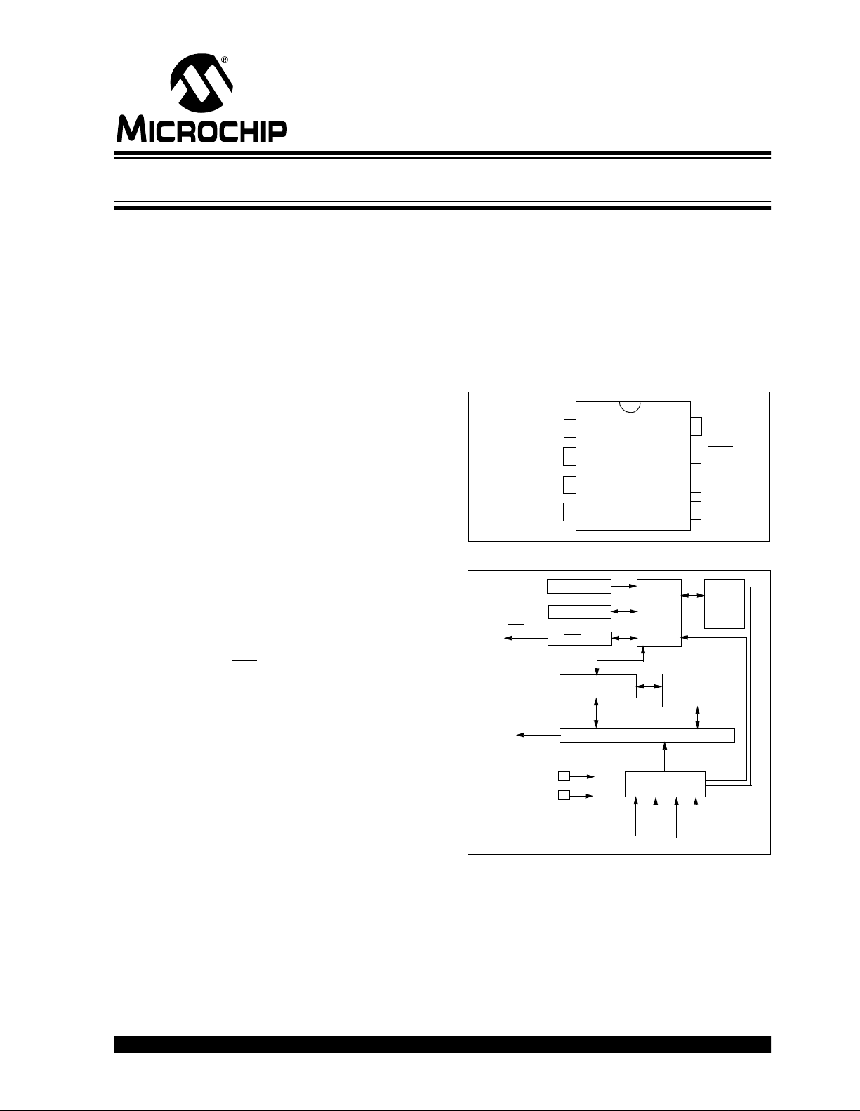
PACKAGE TYPES
PDIP, SOIC
8
V
S0
S1
S2
S3
1
HCS360
2
3
4
DD
LED
7
6
DATA
V
SS
5
BLOCK DIAGRAM
LED
DATA
RESET circuit
VSS
VDD
Oscillator
Controller
LED driver
EEPROM
32-bit shift register
Button input port
Encoder
Power
latching
and
switching
Typical Applications
The HCS360 is ideal for Remote Keyless Entry (RKE)
applications. These applications include:
• Automotive RKE systems
• Automotive alarm systems
The HCS360 combines a 32-bit hopping code
generated by a nonlinear encryption algorithm, with a
28/32-bit serial number and 7/3 status bits to create a
67-bit transmission stream.
S
S
S1S
2
3
0
• Automotive immobilizers
• Gate and garage door openers
• Identity t okens
• Burglar alarm systems
2002 Microchip Technology Inc. DS40152E-page 1
Page 2

HCS360
The crypt key, serial number and conf iguration d ata are
stored in an EEPROM array which is n ot accessible via
any external connection. The EEPROM data is programmable but read-protected. The data can be verified only after an automatic erase and programming
operation. This protects against attempts to gain
access to keys or manipulate synchronizat ion values.
The HCS360 provides an easy-to-use serial interface
for programming the necessary keys, system parameters and configuration data.
1.0 SYSTEM OVERVIEW
Key Terms
The following is a l ist of key te rms us ed thro ughout this
data sheet. For additional information on K
Code Hopping, refer to Technical Brief 3 (TB003).
• RKE - Remote Keyless Entry
• Button Status - Indicates what button input(s)
activated the transmission. Encompasses the 4
button status bits S3, S2, S1 and S0 (Figure 3-1).
• Code Hopping - A method by which a code,
viewed externally to the system, appears to
change unpredictably each time it is transmitted.
• Code word - A block of data that is repeatedly
transmitted upon button activation (Figure3-1).
• Transmission - A data stream consisting of
repeating code words (Figure 8-1).
• Crypt key - A unique and secret 64-bit number
used to encrypt and decrypt data. In a symmetrical block cipher such as the K
the encryption and de cry pti on k ey s a re equal and
will therefore be referred to generally as the crypt
key.
• Encoder - A device that generates and encodes
data.
• Encryption Algorithm - A recipe wher eby data i s
scrambled using a cryp t key . The dat a can only be
interpreted by the respe ctive dec ryptio n algo rithm
using the same crypt key.
• Decoder - A device that decodes data received
from an encoder.
• Decryption algorithm - A recipe whereby data
scrambled by an encryption algorithm can be
unscrambled using the s ame crypt key.
EELOQ algorithm,
EELOQ and
• Learn – Learning involves the receive r calculatin g
the transmitter’s appropriate crypt ke y, d ec rypting
the received hopping code and storing the serial
number, synchronization counter value and crypt
key in EEPROM. The K
itates several learning strategies to be implemented on the decoder. The following are
examples of what can be done.
- Simple Learning
The receiver uses a fixed crypt key, common
to all compone nts of al l s y ste ms b y the same
manufacturer, to decrypt the received code
word’s encrypted portion.
- Normal Learning
The receiver uses information transmitted
during normal operation to derive the crypt
key and decrypt the received code word’s
encrypted portion.
- Secure Learn
The transmitter is activated through a special
button combinat ion to t ransmit a stored 60-bit
seed value used to generat e the trans mitter’s
crypt key. The receiver uses this seed value
to derive the same crypt key and decrypt the
received code word’s encrypted portion.
• Manufacturer’s code – A unique and secret 64-
bit number used to generate un ique encoder crypt
keys. Each encoder is programmed with a crypt
key that is a function of the manufacturer’s code.
Each decoder is programmed with the manufacturer code itself.
The HCS360 code hopping encode r is designed sp ecifically for keyless entry systems; primarily vehicles and
home garage door openers. The encoder portion of a
keyless entry system is integrated into a transmitter,
carried by the user and operated to gain access to a
vehicle or restricted area. The HCS360 is meant to be
a cost-effective yet secure solution to such systems,
requiring very few external components (Figure 2-1).
Most low-end keyless entry transmitters are given a
fixed identificati on code that is transmitted ever y time a
button is pushed. The number of unique identification
codes in a low-end system is usually a relatively small
number. These shortcomings provide an opportunity
for a soph istic ated t hief to crea te a d evice that ‘grab s’
a transmission and retransmits it later, or a device that
quickly ‘scans ’ all pos sible identi ficati on c odes un til the
correct one is found.
The HCS360, on the other hand, employs the K
code hopping technology coupled with a transmission
length of 66 bits to virtually eliminate the use of code
‘grabbing’ or code ‘scann ing’. The hig h security le vel of
the HCS360 is ba sed on the p ate nted K
ogy. A block cipher based on a block length of 32 bits
and a key length of 64 bits is used. The algorithm
obscures the informati on i n such a way that even if th e
transmission informati on (before c oding) dif fers b y only
one bit from that of the previous transmission, the next
EELOQ product family facil-
EELOQ
EELOQ
technol-
DS40152E-page 2 2002 Microchip Technology Inc.
Page 3
HCS360
coded transmission will be completely different. Statistically, if only one bit in the 32-bit string of information
changes, greater than 50 percent of the coded transmission bits will change.
As indicated in the block diagram on page one, the
HCS360 has a small EEPROM array which must be
loaded with several p arameters before use; mos t ofte n
programmed by the manufacturer at the time of production. The most important of these are:
• A 28-bit serial number, typically unique for every
encoder
• A crypt key
• An initial 16-bit synchronization value
• A 16-bit configuration value
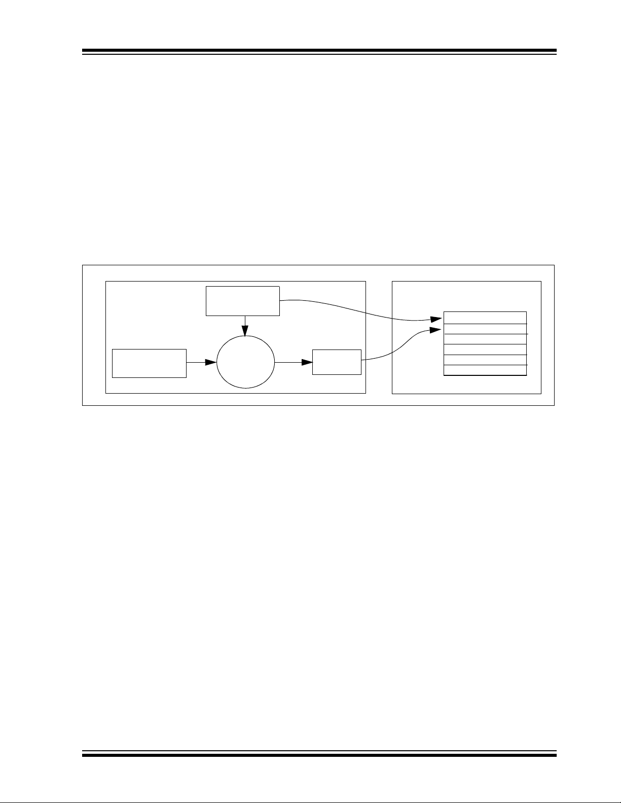
The crypt key generatio n typically input s the transmitter
serial number and 64-bit manufact urer ’s code into t he
key generation algorithm (Figure 1-1). The manufacturer’s code is chosen by the system manufacturer and
must be carefully controlled as it is a pivotal part of the
overall system security.
FIGURE 1-1: CREATION AND STORAGE OF CRYPT KEY DURING PRODUCTION
Production
Programmer
Manufacturer’s
Code
Transmitter
Serial Number
Key
Generation
Algorithm
Crypt
Key
HCS360
EEPROM Array
Serial Number
Crypt Key
Sync Counter
.
.
.
The 16-bit synchronization counter is the basis behind
the transmitted code word changing for each transmission; it increments each time a button is pressed. Due
to the code hoppin g algorith m’s complex ity, each i ncrement of the synchronization value results in greater
than 50% of the bits changing in the transmitted code
word.
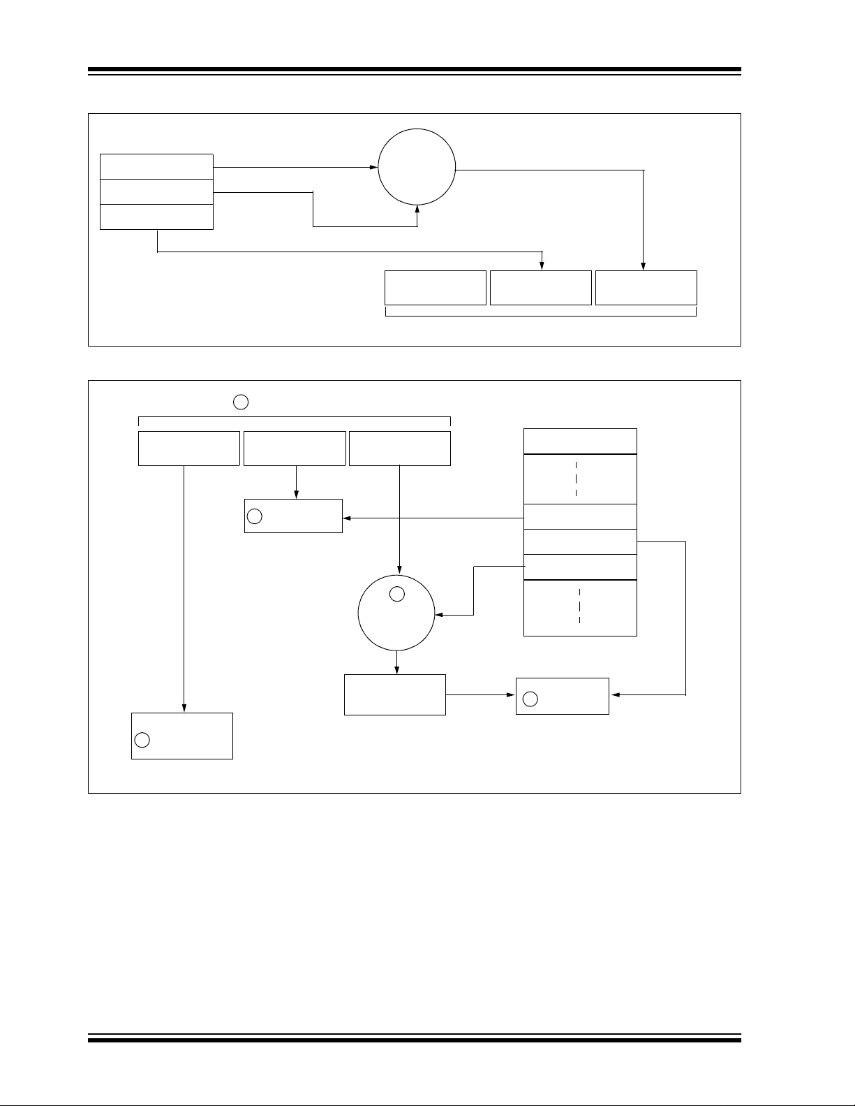
Figure 1-2 shows how the key values in EEPROM are
used in the encoder . O nce the encoder dete cts a button
press, it reads the button inputs and updates the synchronization counter. The synchronization counter and
crypt key are input to the encryption algorithm and the
output is 32 bits of encrypted information. This data will
change with every button press, its value appearing
externally to ‘ran domly h op aroun d’, hence it is re ferred
to as the hopping portion of the code word. The 32-bit
hopping code is combined with the button information
and serial numb er to fo rm the code word transm itted to
the receiver. The code word format is explained in
greater detail in Section 4.2.
A receiver may use any type of controller as a decoder,
but it is typically a microcontroller with compatible firmware that allows the decoder to operate in conjunction
with an HCS360 based transmitter. Section 7.0
provides detail on integrating the HCS360 into a system.
A transmitter must first be ‘learned’ by the receiver
before its use is allowed in the system. Learning
includes calculating the transmitter’s appropriate crypt
key, decrypting the received hopping code and storing
the serial number, synchronization counter value and
crypt key in EEPROM.
In normal operation, each received message of valid
format is evaluated. The serial number is used to determine if it is from a learned transmitter. If from a learned
transmitter, the message is decrypted and the synchronization counter is verified. Finally, the button status is
checked to see what operation is requested. Figure 1-3
shows the relationship between some of the values
stored by the receiver and the values received from
the transmitter.
2002 Microchip Technology Inc. DS40152E-page 3
Page 4
HCS360
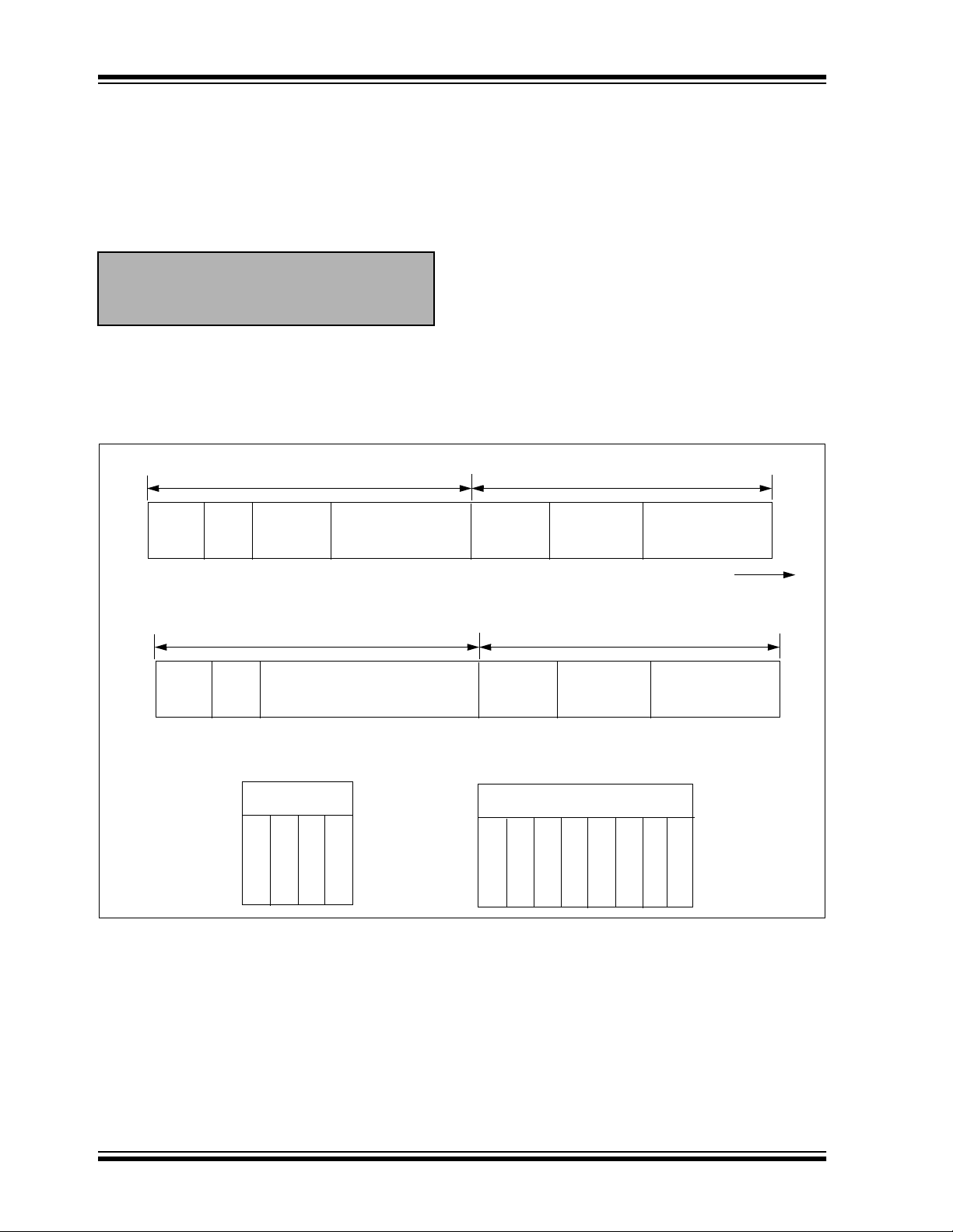
FIGURE 1-2: BUILDING THE TRANSMITTED CODE WORD (ENCODER)
EEPROM Array
Crypt Key
Sync Counter
Serial Number
KEELOQ
Encryption
Algorithm
Button Press
Information
Serial Number
Transmitted Information
FIGURE 1-3: BASIC OPERATION OF RECEIVER (DECODER)
1
Received Information
Button Press
Information
Serial Number
Check for
2
Match
32 Bits of
Encrypted Data
32 Bits
Encrypted Data
EEPROM Array
Manufacturer Code
Serial Number
Sync Counte r
KEELOQ
Decryption
Algorithm
Decrypted
Synchronization
Counter
Perform Function
Indicated by
5
button press
NOTE: Circled numbers indicate the order of execution.
Crypt Key
3
Check for
4
Match
DS40152E-page 4 2002 Microchip Technology Inc.
Page 5

HCS360
2.0 DEVICE OPERATION
As shown in the typical a pplication circ uits (Figu re 2-1),
the HCS360 is a simple device to use. It requires only
the addition of buttons and RF circuitry for use as the
transmitter in your security applic ation. A descripti on of
each pin is described in Table2-1.
FIGURE 2-1: TYPICAL CIRCUITS
VDD
B0
B1
S0
S1
S2
S3
Two button remote control
VDD
LED
DATA
V
SS
Tx out
discrimination value and button information will be
encrypted to form the hopping code. The hopping code
portion will change every transmission, even if the
same button is pushed again. A code word that has
been transmitted will not repeat for more than 64K
transmissions. Thi s provides mo re than 18 years of use
before a code is repeated; based on 10 operations per
day . Overflow inform ation sent from the enc oder can be
used to extend the number of unique transmissions to
more than 192K.
If in the tr an smit proc ess it i s de tec ted t hat a n ew b utton(s) has been pressed, a RESET will immediately
occur and the current cod e word will no t be compl eted.
Please note that buttons removed will not have any
effect on the code word unless no buttons remain
pressed; in which c ase the code word will be compl eted
and the power-down will occur.
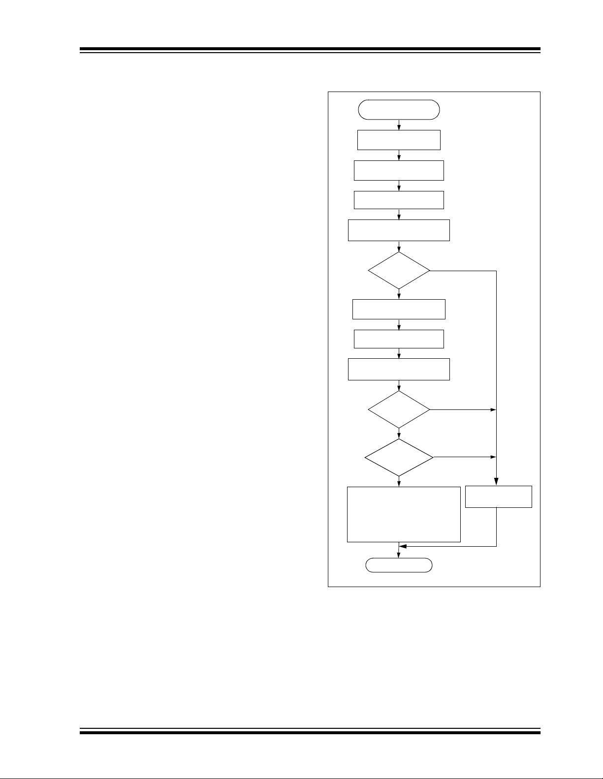
FIGURE 2-2: ENCODER OPERATION
TABLE 2-1: PIN DESCRIPTIONS
Name
S0 1 Switch input 0
S1 2 Switch input 1
S2 3 Switc h input 2 / Clock pin when in
S3 4 Switch input 3
SS 5 Ground reference
V
DATA 6 Data output pin /Data I/O pin for
LED
VDD 8 Positive supply voltage
The HCS360 will wake-up upon detecting a button
press and delay approximately 10 ms for button
debounce (Figure 2-2). The synchronization counter,
2002 Microchip Technology Inc. DS40152E-page 5
Pin
Number
Description
Programming mode
Programming mode
7 Cathode connection for LED
Page 6

HCS360
3.0 EEPROM MEMORY ORGANIZATION
The HCS360 contains 192 bits (12 x 16-bit words) of
EEPROM memory (Table 3-1). This EEPROM array is
used to store the crypt key information, synchronization
value, etc . Fu r t he r d es cr i pti o ns of t h e m e mory array is
given in the following sections.
TABLE 3-1: EEPROM MEMORY MAP
WORD
ADDRESS
0 KEY_0 64-bit crypt key
1 KEY_1 64-bit crypt key
2 KEY_2 64-bit crypt key
3 KEY_3 64-bit crypt key
4 SYNC_A 16-bit synch counter
5 SYNC_B/
6 RESERVED Set to 0000H
7SEED_0Seed Value
8SEED_1Seed Value
9SER_0Device Serial Number
10 SER_1 Device Serial Number
11 CONFIG Configuration Word
MNEMONIC DESCRIPTION
(word 0) LSb’s
(word 1)
(word 2)
(word 3) MSb’s
16-bit synch counter B
SEED_2
or Seed value (word 2)
(word 0) LSb’s
(word 1) MSb’s
(word 0) LSb’s
(word 1) MSb’s
3.2 SYNC_A, SYNC_B
(Synchronization Counter)
This is th e 16 -bit syn chr oni zatio n va lue th at is used to
create the hopping code for trans missio n. This value is
incremented after every transmission. Separate synchronization counters can be used to stay synchronized with different receivers.
3.3 SEED_0, SEED_1, and SEED_2
(Seed Word)
The three word (48 bits) seed code will be transmitted
when seed transmission is selected. This allows the system designer to implement the Secure Learn feature or
use this fixed code word as part of a different key generation/tracking process or purely as a fixed code transmission.
Note: Since SEED2 and SYNC_B share the
same memory location, Secure Learn and
Independent mod e trans miss ion (inclu ding
IR mode) are mutually exclusive.
3.4 SER_0, SER_1
(Encoder Serial Number)
SER_0 and SER_1 are the lower and upper words of
the device serial number, respectively. There are 32
bits allocated for the Serial Number and a selectable
configuration bit determines whether 32 or 28 bits will
be transmitted. The serial number is meant to be
unique for every transmitter.
3.1 KEY_0 - KEY_3 (64-Bit Crypt Key)
The 64-bit crypt key is used to create the encrypted
message transmitted to the receiver. This key is calculated and programmed during production using a key
generation algorithm. The key generation algorithm
may be different from the K
the key generation algorithm are typically the transmit-
ter’s serial number and the 64 -bit manufa cturer’s cod e.
While the key generation algorithm supplied from
Microchip is the typical method used, a user may elec t
to create their own m ethod of key gene ration. This ma y
be done providing that the deco der is program med with
the same means of creating the key for
decryption purposes.
DS40152E-page 6 2002 Microchip Technology Inc.
EELOQ
algorithm. Inputs to
Page 7
HCS360
3.5 CONFIG
(Configuration Word)
The Configuration Word is a 16-bit word stored in
EEPROM array that is used by the device to store
information used during the enc ryption proce ss, as well
as the status of option configurations. Further
explanations of each of the bits are described in the
following sections.
TABLE 3-2: CONFIGURATION WORD.
Bit Number Symbol Bit Description
0 LNGRD Long Guard Tim e
1 BSEL 0 Baud Rate Selection
2 BSEL 1 Baud Rate Selection
3 NU Not Used
4 SEED Seed Transmission enable
5 DELM Delay mode enable
6 TIMO Time-out enable
7 IND Independent mode enable
8 USRA0 User bit
9 USRA1 User bit
10 USRB0 User bit
11 USRB1 User bit
12 XSER Extended serial number
enable
13 TMPSD Temporary seed transmis-
sion enable
14 MOD Manchester/PWM modula-
tion selection
15 OVR Overflow bit
3.5.1 MOD: MODULATION FORMAT
MOD selects between Manchester code modulation
and PWM modulation.
If MOD = 1, Manchester modulation is selected:
If MOD = 0, PWM modulation is selected.
BSEL 1 and BSEL 0 determine the baud rate according
to Table3-4 when Manchester modulation is selected.
TABLE 3-4: BAUD RATE SELECTION
MOD BSEL 1 BSEL 0 TE Unit
100800us
101400us
110400us
111200us
3.5.3 OVR: OVERFLOW
The overflow bit is u sed to exten d the nu mber o f poss ible synchronization values. The synchronization
counter is 16 bits in length, yielding 65,536 values
before the cycle repeats. Under typical use of
10 operations a day, this will provide n ea rly 18 years of
use before a repeated value will be used. Should the
system designer conclude that is not adequate, then
the overflow bit can be utiliz ed to exte nd the numbe r of
unique values. This can be do ne by pr ogramming O VR
to 1 at the time of production. The encoder will automatically clear OVR the first time that the transmitted
synchronization value wraps from 0xFFFF to 0x0000.
Once cleared, OVR cannot be set again, thereby crea ting a permanent record of the counter overflow. This
prevents fast cycling of 64K counter . If the dec oder system is programmed to track the overflow bits, then the
effective number of unique synchronization values can
be extended to 128K. If programmed to zero, the system will be compatible with old encoder devices.
3.5.4 LNGRD: LONG GUARD TIME
LNGRD = 1 selects the encoder to extend the guard
time between code words adding ≈50 ms. This can be
used to reduce the average power transmitted over a
100 ms window and thereby transmit a higher peak
power.
3.5.2 BSEL 1, 0
BAUD RATE SELECTION
BSEL 1 and BSEL 0 determin e the baud rate according
to Table 3-3 when PWM mo dulation is selected.
TABLE 3-3: BAUD RATE SELECTION
MOD BSEL 1 BSEL 0 T
000400us
001200us
010200us
011100us
2002 Microchip Technology Inc. DS40152E-page 7
E Unit
Page 8
HCS360
3.5.5 XSER: EXTENDED SERIAL
NUMBER
If XSER = 0, the four Most Significant bits of the Serial
Number are substituted by S[3:0] and the code word
format is co mpatible with the HCS200/300/301.
If XSER = 1, the full 32-bit Serial Number [SER_1,
SER_0] is transmitted.
Note: Since the button status S[3:0] is used to
detect a Seed transmission, Extended
Serial Number and Secure Learn are
mutually exclusive.
FIGURE 3-1: CODE WORD ORGANIZATION
XSER=0
Fixed Code Portion of Transmission Encrypted Portion of Transmission
Button
Status
(4 bits)
28-bit
Serial Number
MSB
CRC
(2-bit)
VLOW
(1-bit)
3.5.6 DISCRIMINATION VALUE
While in other KEELOQ encoders its value is user
selectable, the HCS360 uses directly the 8 Least Significant bits of the Se rial N umber a s part of t he info rmation that form the encrypted portion of the
transmission (Figure 3-1).
The discrimination value aids the post-decryption
check on the decoder end. After the receiver has
decrypted a transmiss ion, the discrimination b its are
checked against the e ncoder Serial Number to verif y
that the decryp tion process was valid.
3.5.7 USRA,B: USER BITS
User bits form part of the discrimi nation valu e. The user
bits together with the IND bit can be used to identify the
counter that is used in Independent mode.
Button
Status
(4 bits)
Discrimination
bits
(12 bits)
16-bit
Sync Value
LSB
XSER=1
MSB
Fixed Code Portion of Transmission Encrypted Portion of Transmission
CRC
(2-bit)
VLOW
(1-bit)
Button Status
(4 bits)
SSSS
2103
Extended Serial Number
32-bit
Button
Status
(4 bits)
I O U U S S ... S
N V S S E E ... E
Discrimination
bits
(12 bits)
Discrimination Bits
(12 bits)
D R R R R R ... R
1 0 7 6 ... 0
67 bits
of Data
Transmitted
16-bit
Sync Value
LSB
DS40152E-page 8 2002 Microchip Technology Inc.
Page 9
HCS360
3.5.8 SEED: ENABLE SEED
TRANSMISSION
If SEED = 0, seed transmission is disabled. The Independent Counter mode can only be used with seed
transmission disable d since SEED_2 i s shared with th e
second synchronization counter.
With SEED = 1, seed transmission is enabled. The
appropriate button code(s) must be activated to transmit the seed information. In this mode, the seed infor-
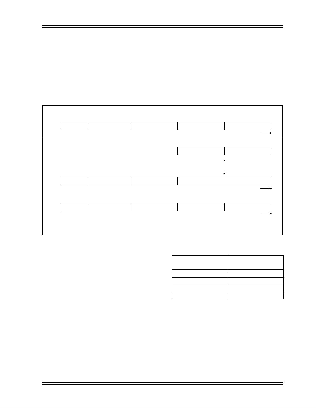
FIGURE 3-2: Seed Transmission
All examples shown with XSER = 1, SEED = 1
When S[3:0] = 1001, delay is not acceptable.
CRC+VLOW SER_1 SEED_2 SEED_1 SEED_0
For S[3:0] = 0x3 before delay:
CRC+VLOW SER_1 SER_0 Encrypted Data
mation (SEED_0, SEED_1, and SEED_2) and the
upper 12 or 16 bits of the serial number (SER_1) are
transmitted instead of the hop code.
Seed transmission is available for function codes
(Table 3-9) S[3:0] = 1001 and S[3:0] = 0011(delayed).
This takes place regardless of the setting of the IND bit.
The two seed transmissions are shown in Figure 3-2.
Data transmission direction
16-bit Data Word 16-bit Counter
Encrypt
Data transmission direction
For S[3:0] = 0011 after delay (Note 1, Note 2):
CRC+VLOW SER_1 SEED_2 SEED_1 SEED_0
Note 1 : For Seed Transmission, SEED_2 is transmitted instead of SER_0.
2: For Seed Transmission, the setting of DELM has no effect.
3.5.9 TMPSD: TEMPORARY SEED
TRANSMISSION
The temporary seed transmission can be used to disable learning after the transmitter has been used for a
programmable number of operations. This feature can
be used to implemen t very secu re systems. After learning is disabled, the seed information cannot be
accessed even if physical access to the transmitter is
possible. If TMPSD = 1 the seed transmission will be
disabled after a number of code hopping transmissions. The number of tra nsmiss ions be fore see d transmission is disabl ed, can be programmed by setting th e
synchronization counter (SYNC_A, SYNC_B) to a
value as shown in Table 3-5.
Data transmission direction
TABLE 3-5: SYNCHRONOUS COUNTER
INITIALIZATION VALUES
Synchronous Counter
Value s
0000H 128
0060H 64
0050H 32
0048H 16
Number of
Transmissions
2002 Microchip Technology Inc. DS40152E-page 9
Page 10

HCS360
3.5.10 DELM: DELAY MODE
If DELM = 1, delay transmission is enabled. A delayed
transmissi on is indic ated by in verting th e lower nib ble
of the discrimination value. The Delay mode is primarily
for compatibil ity with pre vious K
not recommended for new designs.
EELOQ devices and is
TABLE 3-6: TYPICAL DELAY TIMES
Number of Code
BSEL 1 BSEL 0
00 28 ≈ 2.9s ≈ 5.1s
01 56 ≈ 3.1s ≈ 6.4s
10 28 ≈ 1.5s ≈ 3.2s
11 56 ≈ 1.7s ≈ 4.5s
Words before Delay
Mode
3.5.11 TIMO: TIME-OUT
OR AUTO-SHUTOFF
If TIMO = 1, the time-out is enabled. Time-out can be
used to terminate accid ental c ontinuous tran smissions.
When time-out occurs, the PWM output is set low and
TABLE 3-7: TYPICAL TIME-OUT TIMES
If DELM = 0, delay transmission is disabled (Table 3-
6).
Time Before Delay Mode
(MOD = 0)
the LED is turned off. Current consumption will be
higher than in Standby mode since current will flow
through the activated input resistors. This state can be
exited only after al l in put s are taken low. TIMO = 0, will
enable continuous transmission (Table 3-7).
Time Before Delay Mode
(MOD = 1)
Maximum Number of
BSEL 1 BSEL 0
00 256 ≈ 26.5s ≈ 46.9
01 512 ≈ 28.2s ≈ 58.4
10 256 ≈ 14.1s ≈ 29.2
11 512 ≈ 15.7s ≈ 40.7
Code Words
Transmitted
Time Before Time-out
(MOD = 0)
Time Before Time-out
(MOD = 1)
DS40152E-page 10 2002 Microchip Technology Inc.
Page 11
HCS360
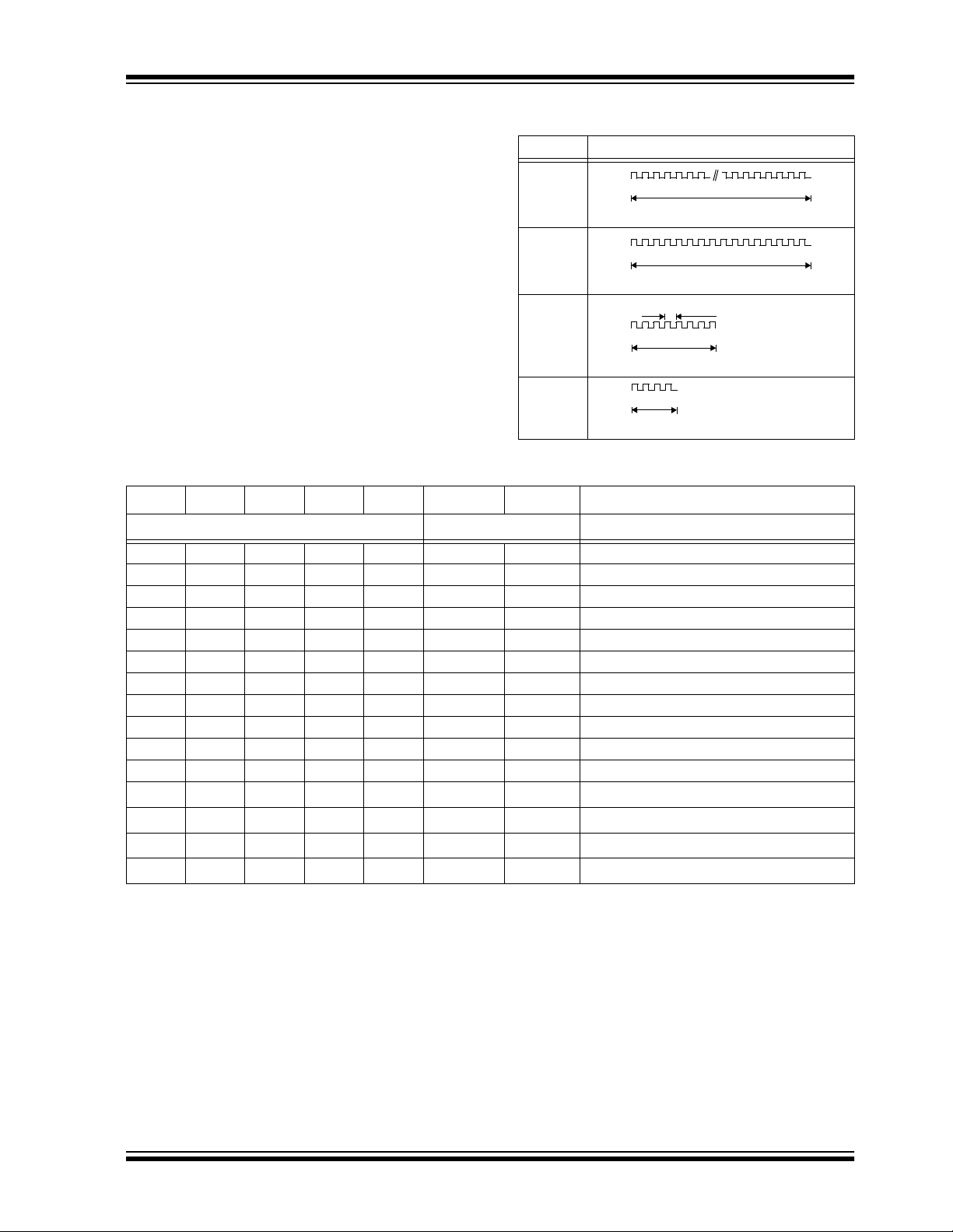
3.5.12 IND: INDEPENDENT MODE
The Independent mode can be used where one
TABLE 3-8: IR MODULATION
T
E Basic Pulse
encoder is used to co ntro l tw o re ce iv ers . Two counters
(SYNC_A and SYNC_B) are used in Independent
mode. As indicated in Table 3-9, function codes 1 to 7
use SYNC_A and 8 to 15 SYNC_B.
800us
(800µs)
(32x)
3.5.13 INFRARED MODE
The Independent mode also selects IR mode. In IR
400us
mode functi on codes 12 to 15 will use SYNC_B. T he
PWM output signal is modulated with a 40 kHz carrier
(see Table 3-8). It must be pointed out that the 40 kHz
is derived from the inte rnal cloc k and wil l therefore vary
200us
(200µs)
with the same percentage as the baud rate. If IND = 0,
SYNC_A is used for all fun ction code s. If IND = 1, Independent mode is enabled and counters for functions
are used according to Table 3-9.
TABLE 3-9:
FUNCTION CODES
100us
(100µs)
(4x)
S3 S2 S1 S0 IND = 0 IND = 1 Comments
Counter
10001 A A
20010 A A
3 0 0 1 1 A A If SEED = 1, transmit seed after delay.
40100 A A
50101 A A
60110 A A
70111 A A
81000 A B
9 1 0 0 1 A B If SEED = 1, transmit seed immediately.
101010 A B
111011 A B
121100 A
131101 A
141110 A
151111 A
(1)
B
(1)
B
(1)
B
(1)
B
Note 1: IR mode
(400µs)
(16x)
Period = 25µs
(8x)
2002 Microchip Technology Inc. DS40152E-page 11
Page 12

HCS360
4.0 TRANSMITTED WORD
4.1 Transmission Format (PWM)
The HCS360 code word is made up of several parts
(Figure 4-1 and Figure 4-2). Each code word contains
a 50% duty cycle preamble, a header, 32 bits of
encrypted data and 35 bits of fixed data followed by a
guard period before another code word can begin.
Refer to T able8-3 and Table 8-5 for code word timing.
FIGURE 4-1: CODE WORD FORMAT (PWM)
50% Duty Cycle
Preamble
1
16
4.2 Code Word Organization
The HCS360 transmit s a 67 -bit code word when a button is pressed. The 67-bit word is constructed from a
Fixed Code portion and an Encrypted Code portion
(Figure 3-1).
The Encrypted Data is generated from 4 function bits,
2 user bits, overflow bit, Independent mode bit, and 8
serial number bits, and the 16-b it synchronization value
(Figure 3-1). The encrypted portion alone provides up
to four billion changing code combinations.
The Fixe d Code Data is made up of a V
bits, 4 function bits, and the 28-bit serial number. If the
extended serial numb er (32 bits) is s elected, the 4 func tion code bits will not be transmitted. The fixed and
encrypted sections combined increase the number of
code combinations to 7.38 x 10
LOGIC "0"
LOGIC "1"
19
LOW bit, 2 CRC
TETET
E
31XTE Encrypted Portion Fixed Portion
Preamble
10xTE
Header
of Transmission
FIGURE 4-2: CODE WORD FORMAT (MANCHESTER)
50% Duty Cycle
Preamble
1
2
31XTE
Preamble
START bit
16
4XTE
Header
bit 0
bit 2
bit 1
Encrypted Portion Fixed Portion
of Transmission of Transmission
of Transmission
LOGIC "0"
LOGIC "1"
Guard
STOP bit
Time
T
E
Guard
Time
TE
DS40152E-page 12 2002 Microchip Technology Inc.
Page 13

HCS360
5.0 SPECIAL FEATURES
5.1 Code Word Completion
Code word completion is an automatic feature that
ensures th at th e en tire cod e wor d i s tran smi tte d, e ven
if the button is rel eased before the transmissi on is complete and that a minimum of two words are completed.
The HCS360 encode r powers i tself up when a button is
pushed and powers itself down after two complete
words are transmitted if the user has already released
the button. If the button is held down beyond the time
for one transmission, then multiple transmissions will
result. If another button is activated during a
transmission, the active transmission will be aborted
and the new code will be generated using the new
button information.
5.2 Long Guard Time
Federal Communications Commission (FCC) part 15
rules specify the limits on fundamental power and
harmonics that can be transmitted. Power is calculated
on the worst case average power transmitted in a 100
ms window. It is therefore advantageous to minimize
the duty cycle of the transmitted word. This can be
achieved by minimizing the duty cycle of the individual
bits or by extending the guard time between transmissions. Long guard time (LNGRD) is used for reducing
the average power of a transmission. This is a selectable feature. Using the LNGRD allows the user to
transmit a higher amplitude transmission if the
transmission time pe r 10 0 m s is shorter. The FCC puts
constraints on the average power that can be
transmitted by a device, and LNGRD effectively
prevents continuous transmission by only allowing the
transmission of every seco nd word. This reduces the
average power transmitted and hence, assists in FCC
approval of a transmitter device.
5.3 CRC (Cycle Redundancy Check)
Bits
The CRC bits are calcul ated on the 65 previously trans mitted bits. The CRC bits can be used by the receiver
to check the dat a integrity before processi ng start s. The
CRC can detect all single bit and 66% of double bit
errors. The CRC is computed as follows:
EQUATION 5-1: CRC Calculation
CRC 1[]
and
CRC 0[]
with
and
Di
the nth transmission bit 0 ≤ n ≤ 64
n
Note: The CRC may be wrong when the battery
. Work around: If the CRC calculation is incor-
n 1+
CRC 10,[]
voltage is around either of the V
points. This may happen because V
sampled twice each transmission, once for
the CRC calculation (PWM is low) and once
when V
V
sion which could lead to a different value for
V
and the transmission
rect, recalculate for the opposite value of
V
LOW is transmitted (PWM is high).
DD tends to move sligh tly during a transmis -
LOW being used for the CRC calculation
LOW.
CRC 0[]nDin∧=
n 1+
CRC 0[]nDin∧()CRC 1[]
0
∧=
0=
n
LOW trip
LOW is
2002 Microchip Technology Inc. DS40152E-page 13
Page 14

HCS360
5.4 Auto-shutoff
The Auto-shutoff function automatically stops the
device from transmitting if a button inadvertently gets
pressed fo r a lo ng p eri od of tim e. Th is w ill prev ent the
device from draining the battery if a button gets
pressed whil e the transmitte r is in a pocket or purse .
This function can be enabled or disabled and is
selected by setting or clearing the time-out bit
(Section 3.5.1 1). Setti ng this bit wil l enab le the f unctio n
(turn Auto-shutoff function on) and clearing the bit will
disable the function. Time-out period is approx imately
25 seconds.
5.5 VLOW: Voltage LOW Indicator
The VLOW bit is transmitted with every transmission
(Figure 3-1) and will be transmitted as a one if the
operating voltage has dropped below the low voltage
trip point, typically 3.8V at 25°C. This V
LOW signal is
transmitted so the receiver c an give an indicati on to the
user that the transmitter battery is low.
5.6 LED Output Operation
During normal transmission the LED output is LOW
while the data is being transmitted and high during the
guard time. Two voltage indications are combined into
one bit: V
of V
LOW. Table 5-1 indicates the operation value
LOW while data is being transmitted.
FIGURE 5-1: VLOW Trip Point VS.
Temperature
4.5
V
3.5
2.5
1.5
LOW=0
4
LOW=1
3
2
-40
V
LOW=0
V
Nominal Trip Point
3.8V
Nominal Trip
Point
25 85
3.5
2V
If the supply voltage drops below the low voltage trip
point, the LED
output will be toggl ed at appr oximate ly
1Hz during the transmission.
TABLE 5-1: VLOW AND LED VS. VDD
Approximate
Supply Voltage
Max → 3.8V 0 Normal
3.8V → 2.2V 1 Flashing
2.2V → Min 0 Normal
LOW Bit LED Operation*
V
*See also FLASH operating modes.
DS40152E-page 14 2002 Microchip Technology Inc.
Page 15
HCS360
6.0 PROGRAMMING THE HCS360
When using the HCS360 in a s ystem, the user will have
to program some parameters into the device including
the serial number and the secret key before it can be
used. The programming allows the user to input all 192
bits in a serial dat a stre am, whi ch are then stored internally in EEPROM. Programming will be initiated by
forcing the PWM line high, after the S3 line has been
held high for the appropriate length of time. S0 should
be held low during the entir e program cycle . The S1
line on the HCS360 part needs to be set or cleared
depending on the LS bit of the memory map (Key 0)
before the ke y is clocked in to the HCS360. S1 must
remain at this l evel for the duratio n of the p rogramm ing
cycle. The device can the n be programmed by clocking
FIGURE 6-1: Programming Waveforms
Enter Program
Mode
DATA
(Data)
S2/S3
(Clock)
S1
T
2
T
1
Bit 1 Bit 2 Bit 3 Bit 14 Bit 15
Bit 0
TCLKL
TDH
TDS
Bit 0 of Word0
Data for Word 0 (KEY_0)
TCLKH
Repeat for each word
in 16 bits a t a ti me , followed by the wo rd’s compleme nt
using S3 or S2 as the clock line and PWM as the data
in line. After each 16-b it word is load ed, a programm ing
delay is require d f or t he internal program cy c le to c om plete. The Acknowledge can read back after the programming delay (T
WC). After the first word and its
complement have been downloaded, an automatic
bulk write is performed. This delay can take up to Twc.
At the end of the programming cycl e, the device can be
verified (Figure 6-1) by reading back the EEPROM.
Reading is done by clocking the S3 line and reading the
data bits on PWM . For security reasons, i t is no t possible to execute a Verify function without first programming the EEPROM. A Verify operation can only be
done once, immediately following the Program
cycle.
Acknowledge Pulse
TWC
Bit 0 Bit 1 Bit 2 Bit 3 Bit 14 Bit 15
Bit 16
Data for Word 1
Bit 17
Note 1: Unused button inputs to be held to ground during the entire programming sequence.
The VDD pin must be taken to ground after a program/verify cycle.
2: The V
DD pin must be taken to ground after a Program/Verify cycle.
FIGURE 6-2: Verify Waveforms
End of Programming Cycle Beginning of Verify Cycle
Data from Word0
DATA
(Data)
S2/S3
(Clock)
S1
Ack
Bit 0Bit191Bit190
TWC
Note: A Verify sequence is performed only once immediately after the Program cycle.
Bit 1 Bit 2 Bit 3 Bit 15Bit 14 Bit 16 Bit 17 Bit190 Bit191
TDV
2002 Microchip Technology Inc. DS40152E-page 15
Page 16

HCS360
TABLE 6-3: PROGRAMMING/VERIFY TIMING REQUIREMENTS
DD = 5.0V ± 10%
V
25° C ± 5 °C
Parameter Symbol Min. Max. Units
Program mode setup time T
Hold time 1 T
Program cycle time T
Clock low time T
Clock high time T
Data setup time T
2
1
WC 50 — ms
CLKL 50 — µs
CLKH 50 — µs
DS 0—
Data hold time TDH 30 —
Data out valid time TDV —30
Note 1: Typical values - not tested in production.
04.0ms
9.0 —ms
µs
µs
µs
(1)
(1)
(1)
DS40152E-page 16 2002 Microchip Technology Inc.
Page 17
HCS360
7.0 INTEGRATING THE HCS360 INTO A SYSTEM
Use of the HCS360 in a system requires a compatible
decoder . This decoder is typically a microco ntroller with
compatible firmware. Microchip will provide (via a
license agreement) firmware routines that accept
transmissions from the HCS360 and decrypt the
hopping code portion of the data stream. These
routines provide system designers the means to
develop their own decoding system.
7.1 Learning a Transmitter to a
Receiver
A transmitter must first be ’ learned’ by a decoder before
its use is allowed in the system. Several learning strategies are possible, Figure 7-1 details a typical learn
sequence. Core to each, the decoder must minimally
store each learned trans mitter’ s seri al nu mber and c urrent synchronization counter value in EEPROM. Additionally, the decoder typically stores each transmitter’s
unique crypt key. The maximum number of learned
transmitters will therefore be relative to the available
EEPROM.
A transmitter’s serial number is transmitted in the clear
but the synchronization counter only exists in the code
word’s encrypted portion. The decoder obtains the
counter value by decrypting using the same key used
to encrypt the information. The K
symmetrical block cipher so the e ncryption and decryption keys are identical and referred to generally as the
crypt key. The encoder receives its crypt key during
manufacturing. The decoder is programmed with the
ability to generate a crypt key as well as all but one
required input to the key generation routine; typically
the transmitter’s serial number.
Figure 7-1 summarizes a typical learn sequence. The
decoder receives and authenticates a first transmission; first button press. Authentication involves generating the ap propriate crypt ke y, decrypting, va lidating
the correct key usage via the discrimination bits and
buffering th e counter v alue. A seco nd transmi ssion is
received and authenticated. A final check verifies the
counter values were sequential; consecutive button
presses. If the learn sequence is successfully complete, the decoder stores the learned transmitter’s
serial number, current synchronization counter value
and appropriate crypt key. From now on the crypt key
will be retrieved from EEPROM during normal operation instead of recalculating it for each transmission
received.
Certain learning strategies have been patented and
care must be taken not to infringe.
EELOQ algorithm is a
FIGURE 7-1: TYPICAL LEARN
SEQUENCE
Enter Learn
Mode
Wait for Reception
of a Valid Code
Generate Key
from Serial Number
Use Generated Key
to Decrypt
Compare Discrimination
Value with Fixed Value
Equal
?
Yes
Wait for Reception
of Second Valid Code
Use Generated Key
to Decrypt
Compare Discrimination
Value with Fixed Value
Equal
?
Yes
Counters
Sequential
?
Yes
Learn successful Store:
Serial number
Encryption key
Synchronization counter
Exit
No
No
No
Learn
Unsuccessful
2002 Microchip Technology Inc. DS40152E-page 17
Page 18
HCS360
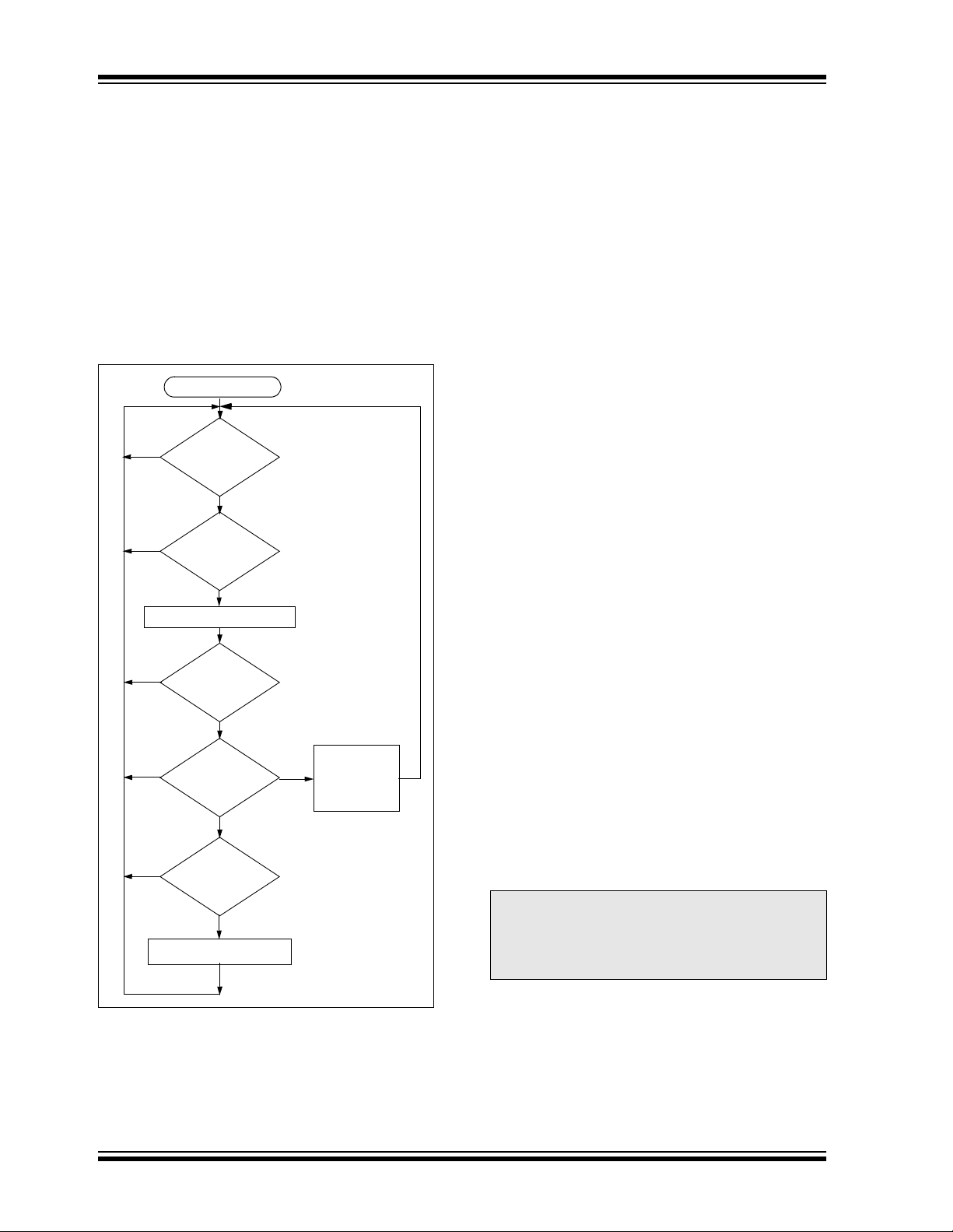
7.2 Decoder Operation
Figure 7-2 summarizes normal d ecoder op eration . The
decoder waits until a transmission is received. The
received serial number is compared to the EEPROM
table of learned transmitters to first determine if this
transmitter’s use is allowed in the system. If from a
learned transmitter, the transmission is decrypted
using the stored crypt key and authenticated via the
discrimination bits for appropriate crypt key usage. If
the decryption was valid the synchronization value is
evaluated.
FIGURE 7-2: TYP ICAL DECODER
OPERATION
Start
No
Transmission
Received
?
Yes
No
Decrypt Transmission
No
No
No
Does
Serial Number
Match
?
Yes
Is
Decryption
Valid
?
Yes
Is
Counter
Within 16
?
No
Is
Counter
Within 32K
?
Yes
Save Counter
in Temp Location
Yes
Execute
Command
and
Update
Counter
7.3 Synchronization with Decoder
(Evaluating the Counter)
The KEELOQ technology patent scope includes a
sophisticated synchronization technique that does not
require the calculation an d storage of future codes. Th e
technique securely blocks invalid transmissions while
providing transparent resynchro niz at ion to transmitters
inadvertently activated away from the receiver.
Figure 7-3 shows a 3-partitio n, rotatin g synchroniza tion
window. The size of each window is optional but the
technique is fundamental. Each time a transmission is
authenticated, the intended function is executed and
the transmission’s synchronization counter value is
stored in EEPROM. From the currently stored counter
value ther e is an initial "Single Operation" forward window of 16 codes. If the difference between a received
synchronization counter and the last stored counter is
within 16, the intended functi on wil l be execu ted on the
single button press and the new synchronization
counter will be sto r ed . Storing the new synchronization
counter value ef fectively rot ates the entire sy nchronization window.
A "Double Operation" (resynchronization) window further exists from the Si ngle Ope ration windo w up to 3 2K
codes forward of the currently stored counter value. It
is referred to as "Double Operation" because a transmission with synchronization counter value in this window will require an additional, sequential counter
transmissi on prior to execut ing the intended function.
Upon receiving the sequential transmission the
decoder executes the intended function and stores the
synchroniz ation co unter va lue. Th is resy nchroniz ation
occurs transparently to the user as it is human nature
to press the button a second t ime if the first was un successful.
The third window is a "Blocked Window" ranging from
the double operation window to the currently stored
synchroniz ation counter value. An y transmission with
synchronization counter value within this window will
be ignored. This window excludes previously used,
perhaps code-grabbed transmissions from accessing
the system.
Note: The synchronization method described in
this section is only a typic al implement ation
and because it is usually implemented in
firmware, it can be altered to fit the needs
of a particular system.
DS40152E-page 18 2002 Microchip Technology Inc.
Page 19

FIGURE 7-3: SYNCHRONIZATION WINDOW
Entire Window
rotates to eliminate
use of previously
used codes
Blocked
Window
(32K Codes)
Double Operation
(resynchronization)
Window
(32K Codes)
HCS360
Stored
Synchronization
Counter Value
Single Operation
Window
(16 Codes)
2002 Microchip Technology Inc. DS40152E-page 19
Page 20

HCS360
8.0 ELECTRICAL CHARACTERISTICS
TABLE 8-1: ABSOLUTE MAXIMUM RATINGS
Symbol Item Rating Units
V
DD Supply voltage -0.3 to 6.9 V
VIN Input voltage -0.3 to VDD + 0.3 V
VOUT Output voltage -0.3 to VDD + 0.3 V
OUT Max output current 25 mA
I
TSTG Storage temperature -55 to +125 °C (Note)
TLSOL Lead soldering temp 300 °C (Note)
ESD ESD rating 4000 V
V
Note: Stresses above those lis ted under “ABSOLUTE MAXIMUM RATINGS” may cause permanent damage to the
device.
TABLE 8-2: DC CHARACTERISTICS
Commercial (C): Tamb = 0°C to +70°C
Industrial (I): Tam b = -40°C to +85°C
2.0V < V
Parameter Sym. Min
Operating current
I
CC 0.3 1.2
(avg)
Standby current I
Auto-shutoff
2,3
current
High level input
CCS 0.1 1.0 0.1 1.0 µA
ICCS 40 75 160 350 µA
V
IH 0.55 VDD VDD+0.3 0.55VDD VDD+0.3 V
voltage
Low level input
V
IL -0.3 0.15 VDD -0.3 0.15VDD V
voltage
High level output
V
OH 0.7 VDD 0.7 V DD VIOH = -1.0 mA, VDD = 2.0V
voltage
Low level output
VOL 0.08 VDD 0.08VDD VIOL = 1.0 mA, VDD = 2.0V
voltage
LED sink current ILED 0.15 1.0 4.0 0.15 1.0 4.0 mA
Pull-Down
S0-34060 80 406080kΩ VDD = 4.0V
R
Resistance; S0-S3
Pull-Down
R
PWM 80 120 160 80 120 160 kΩ VDD = 4.0V
Resistance; DAT A
Note 1: Typical values are at 25°C.
2: Auto-shutoff current specification does not include the current through the input pull-down resistors.
3: Auto-shutoff current is periodically sampled and not 100% tested.
4: VLED is the voltage between the VDD pin and the LED pin.
DD < 3.3 3.0 < VDD < 6.6
1
Typ
Max Min
Typ
0.7 1.6
1
Max Unit Conditions
mA VDD = 3.3V
I
OH = -2.0 mA, VDD = 6.6V
I
OL = 2.0 mA, VDD = 6.6V
4
V
LED
= 1.5V, VDD = 6.6V
DD = 6.6V
V
DS40152E-page 20 2002 Microchip Technology Inc.
Page 21
HCS360
FIGURE 8-1: POWER-UP AND TRANSMIT TIMING
Button Press
PWM
Output
Button
Input
Sn
Detect
T
DB
TTD
BP
T
Code
Word
1
FIGURE 8-2: POWER-UP AND TRANSMIT TIMING REQUIREMENTS
VDD = +2.0 to 6.6V
Commercial (C): T amb = 0°C to +70°C
Industrial (I): Tamb = -40°C to +85°C
Parameter Symbol Min Max Unit Remarks
Time to second button press TBP 10 + Code
Transmit delay from button detect T
Debounce delay T
Auto-shutoff time-out period TTO 15.0 35 s (Note 3)
Note 1: TBP is the time in which a second button can be pressed without completion of the first code word and the
intention was to press the combination of buttons.
2: Transmit delay maximum value if the previous transmission was successfully transmitted.
3: The Auto-shutoff time-out period is not tested.
TD 4.5 26 ms (Note 2)
DB 4.0 13 ms
Multiple Code Word Transmission
Code
Word
2
TTO
Word Time
Code
Word
3
26 + Code
Word Time
Code
Word
4
Code
Word
n
ms (Note 1)
2002 Microchip Technology Inc. DS40152E-page 21
Page 22

HCS360
DS40152E-page 22 2002 Microchip Technology Inc.
Page 23

FIGURE 8-6: MANCHESTER FORMAT SUMMARY (MOD=1)
LOGIC "0"
LOGIC "1"
HCS360
TPB
TE
TE
1
2
50% Duty Cycle
Preamble
31XTE
Preamble
START bit
16
4XTE
Header
bit 0
bit 2
bit 1
Encrypted Portion Fixed Portion
of Transmission of Transmission
FIGURE 8-7: MANCHESTER PREAMBLE/HEADER FORMAT (MOD=1)
50% Duty Cycle
P1
FIGURE 8-8: HCS360 NORMALIZED T
TE
Preamble
31 x TE
1.7
1.6
1.5
1.4
1.3
1.2
1.1
1.0
0.9
0.8
0.7
0.6
-50 -40 -30 -20 -10 0 10 20 30 40 50 60 70 80 90
Preamble
E VS. TEMP
TE Max.
TE Min.
Temperature °C
P16
4 x TE
Header
Typical
STOP bit
Bit 0 Bit 1
Data Word
Transmission
VDD LEGEND
= 2.0V
= 3.0V
= 6.0V
Guard
Time
2002 Microchip Technology Inc. DS40152E-page 23
Page 24

HCS360
TABLE 8-3:
VDD = +2.0V to 6.6V
Commercial (C):Tamb = 0°C to +70°C
Industrial (I):Tamb = -40°C to +85°C
Symbol Characteristic Min. Typ. Max. Min. Typ. Max. Units
T
E Basic pulse element 260 400 620 130 200 310 µs
TBP PWM bit pulse width 3 3 TE
TP Preamble duration 31 31 TE
TH Header duration 10 10 TE
THOP Hopping code duration 96 96 TE
TFIX Fixed code duration 105 105 TE
TG Guard Time (LNGRD = 0) 17 33 TE
— Total transmit time 259 275 TE
— Total transmit time 67.3 103.6 160.6 35.8 55.0 85.3 ms
— PWM data rate 1282 833 538 2564 1667 1075 bps
Note: The timing parameters are not tested but derived from the oscillator clock.
TABLE 8-4:
VDD = +2.0V to 6.6V
Commercial (C):Tamb = 0°C to +70°C
Industrial (I):Tamb = -40°C to +85°C
Symbol Characteristic Min. Typ. Max. Min. Typ. Max. Units
TE Basic pulse element 130 200 310 65 100 155 µs
T
BP PWM bit pulse width 33TE
TP Preamble duration 31 31 TE
TH Header duration 10 10 TE
THOP Ho pping code dur ation 96 96 TE
TFIX Fixed code duration 105 105 TE
TG Guard Time (LNGRD = 0) 33 65 TE
— Total transmit time 275 307 TE
— Total transmit time 35.8 55.0 85.3 20.0 30.7 47.6 ms
— PWM data rate 2564 1667 1075 5128 3333 2151 bps
Note: The timing parameters are not tested but derived from the oscillator clock.
CODE WORD TRANSMISSION TIMING PARAMETERS—PWM MODE
Code Words Transmitted
BSEL1 = 0
BSEL0 = 0
BSEL1 = 0
BSEL0 = 1
CODE WORD TRANSMISSION TIMING PARAMETERS—PWM MODE
Code Words Transmitted
BSEL1 = 1,
BSEL0 = 0
BSEL1 = 1,
BSEL0 = 1
DS40152E-page 24 2002 Microchip Technology Inc.
Page 25

HCS360
TABLE 8-5: CODE WORD TRANSMISSION TIMING PARAMETERS—MANCHESTER MODE
VDD = +2.0V to 6.6V
Commercial (C):Tamb = 0°C to +70°C
Industrial (I):Tamb = -40°C to +85°C
Symbol Characteristic Min. Ty p. Max. Min. Typ. Max. Units
T
E Basic pulse element 520 800 1240 260 400 620 µs
TP Preamble duration 31 31 TE
TH Header duration 4 4 TE
TSTART START bit 2 2 TE
THOP Hopping code duration 64 64 TE
TFIX Fixed code duration 70 70 TE
TSTOP STOP bit 2 2 TE
TG Guard Time (LNGRD = 0) 9 17 TE
— Total transmit time 182 190 TE
— Total transmit time 94.6 145.6 223.7 49.4 76.0 117.8 ms
— Manchester data rate 1923 1250 806 3846.2 2500 1612.9 bps
Note: The timing parameters are not tested but derived from the oscillator clock.
BSEL1 = 0,
BSEL0 = 0
Code Words Transmitted
BSEL1 = 0.
BSEL0 = 1
TABLE 8-6: CODE WORD TRANSMISSION TIMING PARAMETERS—MANCHESTER MODE
VDD = +2.0V to 6.6V
Commercial (C):Tamb = 0°C to +70°C
Industrial (I):Tamb = -40°C to +85°C
BSEL1 = 1,
BSEL0 = 0
Code Words Transmitted
BSEL1 = 1.
BSEL0 = 1
Symbol Characteristic Min. Typ. Max. Min. Typ. Max. Units
T
E Basic pulse element 260 400 620 130 200 310 µs
TP Preamble duration 32 32 TE
TH Header duration 44TE
TSTART START bit 22TE
THOP Hopping code duration 64 64 TE
TFIX Fixed code duration 70 70 TE
TSTOP STOP bit 22TE
TG Guard Time (LNGRD = 0) 16 32 TE
— Total transmit time 190 206 TE
— Total transmit time 49.4 76.0 1 17.8 26.8 41.2 63.4 ms
— Manchester data rate 3846.2 2500.0 1612.9 7692.3 5000.0 3225.8 bps
Note: The timing parameters are not tested but derived from the oscillator clock.
2002 Microchip Technology Inc. DS40152E-page 25
Page 26

HCS360
9.0 PACKAGING INFORMATION
9.1 Package Marking Information
DS40152E-page 26 2002 Microchip Technology Inc.
Page 27
9.2 Package Details
8-Lead Plastic Dual In-line (P) - 300 mil (PDIP)
E
HCS360
α
eB
A
A1
B1
B
A2
L
p
2002 Microchip Technology Inc. DS40152E-page 27
Page 28

HCS360
8-Lead Plastic Small Outline (SN) - Narrow, 150 mil (SOIC)
E
E1
p
D
2
B
Number of Pins
Pitch
Foot Angle
Lead Thickness
Mold Draft Angle Top
Mold Draft Angle Bottom
* Controlling Parameter
§ Significant Characteristic
Notes:
Dimensions D and E1 do not include mold flash or protrusions. Mold flash or protrusions shall not exceed
.010” (0.254mm) per side.
JEDEC Equivalent: MS-012
Drawing No. C04-057
n
°
45
c
β
n
p
φ
c
α
β
1
h
A
φ
L
048048
A1
MILLIMETERSINCHES*Units
1.27.050
α
A2
MAXNOMMINMAXNOMMINDimension Limits
88
1.751.551.35.069.061.053AOverall Height
1.551.421.32.061.056.052A2Molded Package Thickness
0.250.180.10.010.007.004A1Standoff §
6.206.025.79.244.237.228EOverall Width
3.993.913.71.157.154.146E1Molded Package Width
5.004.904.80.197.193.189DOverall Length
0.510.380.25.020.015.010hChamfer Distance
0.760.620.48.030.025.019LFoot Length
0.250.230.20.010.009.008
0.510.420.33.020.017.013BLead Width
1512015120
1512015120
DS40152E-page 28 2002 Microchip Technology Inc.
Page 29

HCS360
ON-LINE SUPPORT
Microchip provides on-line support on the Microchip
World Wide Web (WWW) site.
The web site is used b y Micr ochip as a means to mak e
files and information easily available to customers. To
view the site, the use r must hav e access to the Intern et
and a web browser, such as Netscape or Microsoft
Explorer. Files are also available for FTP download
from our FTP site.
Connecting to the Microchip Internet Web Site
The Microchip web site is available by using your
favorite Internet browser to attach to:
www.microchip.com
The file transfer site is available by using an FTP service to connect to:
ftp://ftp.microchip.com
The web site and file transfer site provide a variety of
services. Users may download files for the latest
Development Tools, Data Sheets, Application Notes,
User’s Guides, Articles and Sample Programs. A variety of Micr ochip specific bu siness informati on is also
available, including listings of Microchip sales offices,
distributors and factory representatives. Other data
available for consideration is:
• Latest Microchip Press Releases
• Technical Support Section with Frequently Asked
Questions
• Design Tips
• Device Errata
• Job Postings
• Microchip Consultant Program Member Listing
• Links to other useful web sites related to
Microchip Products
• Conferences for products , Development System s,
technical information and more
• Listing of seminars and events
Systems Information and Upgrade Hot Line
The Systems Information and Upgrade Line provides
system users a listing of the latest versions of all of
Microchip's development systems software products.
Plus, this line provides information on how customers
can receive any currently available upgrade kits.The
Hot Line Numbers are:
1-800-755-2345 for U.S. and most of Canada, and
1-480-792-7302 for the rest of the world.
2002 Microchip Technology Inc. DS40152E-page 29
Page 30

HCS360
READER RESPONSE
It is our intentio n t o provide you with the best documentati on possible to ensu re s uc ce ss ful us e of your Microchip product. If you wish to pro vide your comm ents on org aniza tion, c larity, subject matter , and w ays in whi ch ou r doc umenta tion
can better serve you, please FAX your comments to the Technical Publications Manager at (480) 792-4150.
Please list the following information, and use this outline to provide us with your comments about this Data Sheet.
To:
RE: Reader Response
From:
Application (optional):
Would you like a reply? Y N
Device:
Questions:
1. What are the best features of this docume nt?
2. How does this document meet your hardware and software development needs?
3. Do you find the organization of this data sheet easy to follow? If not, why?
Technical Publications Manager
Name
Company
Address
City / State / ZIP / Country
Telephone: (_______) _________ - _________
HCS360
Literature Number:
Total Pages Sent
FAX: (______) _________ - _________
DS40152E
4. What additions to the data sheet do you think would enhance the structure and subject?
5. What delet ions from the data sheet could be made without affecti ng the overal l usefulness?
6. Is there any incorrect or misleading information (what and where)?
7. How would you improve this document?
8. How would you improve our software, systems, and silicon products?
DS40152E-page 30 2002 Microchip Technology Inc.
Page 31

HCS360
HCS360 PRODUCT IDENTIFICATION SYSTEM
To order or obtain information, e.g., on pricing or delivery, refer to the factory or the listed sales office.
HCS360 — /P
Package: P = Plastic DIP (300 mil Body), 8-lead
Temperature Blank = 0°C to +70°C
Range: I = –40°C to +85°C
Device: HCS360 Code Hopping Encoder
Sales and Support
Data Sheets
Products supported by a preliminary Data Sheet may have an errata sheet describing minor operational differences and recommended workarounds. To determine if an errata sheet exists for a particular device, please contact one of the following:
1. Your local Microchip sales office
2. The Microchip Corporate Literature Center U.S. FAX: (480) 792-7277
3. The Microchip Worldwide Site (www.microchip.com)
Please specify which device, revision of silicon and Data Sheet (include Literature #) you are using.
New Customer Notification System
Register on our web site (www.microchip.com/cn) to receive the most current information on our products.
SN = Plastic SOIC (150 mil Body), 8-lead
HCS360T Code Hopping Encoder (Tape and Reel)
2002 Microchip Technology Inc. DS40152E-page 31
Page 32

HCS360
NOTES:
DS40152E-page 32 2002 Microchip Technology Inc.
Page 33

Microchip’s Secure Data Products are covered by some or all of the following patents:
Code hopping encoder patents issued in Europe, U.S.A., and R.S.A. — U.S.A.: 5,517,187; Europe: 0459781; R.S.A.: ZA93/4726
Secure learning patents issued in the U.S.A. and R.S.A. — U.S.A.: 5,686,904; R.S.A.: 95/5429
Information contained in this publication regarding device
applications and the like is intended through suggestion only
and may be superseded by updates. It is your responsibility to
ensure that your application meets with your specifications.
No representation or warranty is given and no liability is
assumed by Microchip Technology Incorporated with respect
to the accuracy or use of such information, or infringement of
patents or other intellectual property rights arising from such
use or otherwise. Use of Microchip’s products as critical components in life support systems is not authorized except with
express written approval by Microchip. No licenses are conveyed, implicitly or otherwise, under any intellectual property
rights.
Trademarks
The Microchip name and logo, the Microchip logo, FilterLab,
K
EELOQ, MPLAB, PIC, PICmicro, PICMASTER, PICSTART,
PRO MATE, SEEVAL and The Embedded Control Solutions
Company are registered trademarks of Microchip Technology
Incorporated in the U.S.A. and other countries.
dsPIC, ECONOMONITOR, FanSense, FlexROM, fuzzyLAB,
In-Circuit Serial Programming, ICSP, ICEPIC, microID,
microPort, Migratable Memory, MPASM, MPLIB, MPLINK,
MPSIM, MXDEV, PICC, PICDEM, PICDEM.net, rfPIC, Select
Mode and Total Endurance are trademarks of Microchip
Technology Incorporated in the U.S .A .
Serialized Quick Turn Programming (SQTP) is a service mark
of Microchip Technology Incorporated in the U.S.A.
All other trademarks mentioned herein are property of their
respective companies.
© 2002, Microchip Technology Incorporated, Printed in the
U.S.A., All Rights Reserved.
Printed on recycled paper.
Microchip received QS-9000 quality system
certification for its worldwid e head qu art ers,
design and wafer fabrication facilities in
Chandler and Tempe, Arizona in July 1999. The
Company’s quality system processes and
procedures are QS-9000 compliant for its
PICmicro
devices, Serial EEPROMs and microperipheral
products. In addition, Microchip’s quality
system for the design and manufacture of
development systems is ISO 9001 certified.
®
8-bit MCUs, KEELOQ
®
code hoppin g
2002 Microchip Technology Inc. DS40152E - page 33
Page 34

AMERICAS
Corporate Office
2355 West Chandler Blvd.
Chandler, AZ 85224-6199
Tel: 480-792-7200 Fax: 480-792-7277
Technical Support: 480-792-7627
Web Address: http://www.microchip.com
Rocky Mountain
2355 West Chandler Blvd.
Chandler, AZ 85224-6199
Tel: 480-792-7966 Fax: 480-792-7456
Atlanta
500 Sugar Mill Road, Suite 200B
Atlanta, GA 30350
Tel: 770-640-0034 Fax: 770-640 -03 07
Boston
2 Lan Drive, Suite 120
Westford, MA 01886
Tel: 978-692-3848 Fax: 978-692 -38 21
Chicago
333 Pierce Road, Suite 180
Itasca, IL 60143
Tel: 630-285-0071 Fax: 630-285-0075
Dallas
4570 Westgrove Drive, Suite 160
Addison, TX 75001
Tel: 972-818-7423 Fax: 972-818 -29 24
Detroit
Tri-Atria Office Building
32255 Northwestern Highway, Suite 190
Farmington Hills, MI 48334
Tel: 248-538-2250 Fax: 248-538-2260
Kokomo
2767 S. Albright Road
Kokomo, Indiana 46902
Tel: 765-864-8360 Fax: 765-864-8387
Los Angeles
18201 Von Karman, Suite 1090
Irvine, CA 92612
Tel: 949-263-1888 Fax: 949-263 -13 38
New York
150 Motor Parkway, Suite 202
Hauppauge, NY 11788
Tel: 631-273-5305 Fax: 631-273 -53 35
San Jose
Microchip Technology Inc.
2107 North First Street, Suite 590
San Jose, CA 95131
Tel: 408-436-7950 Fax: 408-436 -79 55
Toronto
6285 Northam Drive, Suite 108
Mississauga, Ontario L4V 1X5, Canada
Tel: 905-673-0699 Fax: 905-673-6509
ASIA/PACIFIC
Australia
Microchip Technology Australia Pty Ltd
Suite 22, 41 Rawson Street
Epping 2121, NSW
Australia
Tel: 61-2-9868-6733 Fax: 61-2-9868-6755
China - Beijing
Microchip Technology Consulting (Shanghai)
DS40152E-page 34 2002 Microchip Technology Inc.
 Loading...