

Page 1

HCS301
KEELOQ® Code Hopping Encoder
FEATURES
Security
•Programmable 28-bit serial number
•Programmable 64-bit encryption key
•Each transmission is unique
•66-bit transmission code length
•32-bit hopping code
•34-bit fixed code (28-bit serial number,
4-bit button code, 2-bit status)
•Encryption keys are read protected
Operating
•3.5V - 13.0V operation
•Four button inputs
•No additional circuitry required
•15 functions available
•Selectable baud rate
•Automatic code word completion
•Battery low signal transmitted to receiver
•Battery low indication on LED
•Non-volatile synchronization data
Other
•Functionally identical to HCS300
•Easy-to-use programming interface
•On-chip EEPROM
•On-chip oscillator and timing components
•Button inputs have internal pull-down resistors
•Current limiting on LED
•Low external component cost
Typical Applications
output
DESCRIPTION
The HCS301 from Microchip Technology Inc. is a code
hopping encoder designed for secure Remote Keyless
Entry (RKE) systems. The HCS301 utilizes the KEELOQ
code hopping technology, which incorporates high
security, a small package outline and low cost, to make
this device a perfect solution for unidirectional remote
keyless entry systems and access control systems.
PACKAGE TYPES
PDIP, SOIC
8
S0
S1
S2
S3
1
2
3
4
HCS301
VDD
LED
7
6
PWM
V
SS
5
HCS301 BLOCK DIAGRAM
LED
PWM
Oscillator
RESET circuit
LED
VSS
VDD
Controller
driver
EEPROM
32-bit shift register
Button input port
Power
latching
and
switching
Encoder
The HCS301 is ideal for Remote Keyless Entry (RKE)
applications. These applications include:
•Automotive RKE systems
•Automotive alarm systems
•Automotive immobilizers
•Gate and garage door openers
•Identity tokens
•Burglar alarm systems
2001 Microchip Technology Inc. DS21143B-page 1
The HCS301 combines a 32-bit hopping code,
generated by a nonlinear encryption algorithm, with a
28-bit serial number and 6 information bits to create a
66-bit code word. The code word length eliminates the
threat of code scanning and the code hopping mechanism makes each transmission unique, thus rendering
code capture and resend schemesuseless.
S3
S2
S1 S0
Page 2

HCS301
The crypt key, serial number and conf iguration dat a are
stored in an EEPROM array which is n ot accessible via
any external connection. The EEPROM data is programmable but read-protected. The data can be verified only after an automatic erase and programming
operation. This protects against attempts to gain
access to keys or manipulate synchronizat ion values.
The HCS301 provides an easy-to-use serial interface
for programming the necessary keys, system parameters and configuration data.
1.0 SYSTEM OVERVIEW
Key Terms
The following is a l ist of key te rms us ed thro ughout this
data sheet. For additional information on K
Code Hopping, refer to Technical Brief 3 (TB003).
• RKE - Remote Keyless Entry
• Button Status - Indicates what button input(s)
activated the transmission. Encompasses the 4
button status bits S3, S2, S1 and S0 (Figure 4-2).
• Code Hopping - A method by which a code,
viewed externally to the system, appears to
change unpredictably each time it is transmitted.
• Code word - A block of data that is repeatedly
transmitted upon button activation (Figure4-1).
• Transmission - A data stream consisting of
repeating code words (Figure 8-2).
• Crypt key - A unique and secret 64-bit number
used to encrypt and decrypt data. In a symmetrical block cipher such as the K
the encryption and de cry pti on k ey s a re equal and
will therefore be referred to gene rally as the crypt
key.
• Encoder - A device that generates and encodes
data.
• Encryption Algorithm - A recipe whereb y data i s
scrambled using a crypt k ey . The dat a can only be
interpreted by the respe ctive dec ryptio n algo rithm
using the same crypt key.
• Decoder - A device that decodes data received
from an encoder.
• Decryption algorithm - A recipe whereby data
scrambled by an encryption algorithm can be
unscrambled using the same crypt key.
EELOQ algorithm,
EELOQ and
• Learn – Learning inv olves the recei ver calcula ting
the transmitter’s appropriate crypt key, d ec ryp ting
the received hopping code and storing the serial
number, synchronization counter value and crypt
key in EEPROM. The K
itates several learning strategies to be implemented on the decoder. The following are
examples of what can be done.
- Simple Learning
The receiver uses a fixed crypt key, common
to all components of all system s by the same
manufacturer, to decrypt the received code
word’s encrypted portion.
- Normal Learning
The receiver uses information transmitted
during normal operation to derive the crypt
key and decrypt the received code word’s
encrypted portion.
- Secure Learn
The transmitter is activated through a special
button combinat ion to t ransmit a stored 60-bit
seed value used to generat e the trans mitter’s
crypt key. The receiver uses this seed value
to derive the same crypt key and decrypt the
received code word’s encrypted portion.
• Manufacturer’s code – A unique and secret 64-
bit number used to generate un ique encoder crypt
keys. Each encoder is programmed with a crypt
key that is a function of the manufacturer’s code.
Each decoder is programmed with the manufacturer code itself.
The HCS301 code hopping encode r is designed sp ecifically for keyless entry systems; primarily vehicles and
home garage door openers. The encoder portion of a
keyless entry system is integrated into a transmitter,
carried by the user and operated to gain access to a
vehicle or restricted area. The HCS301 is meant to be
a cost-effective yet secure solution to such systems,
requiring very few external components (Figure 2-1).
Most low-end keyless entry transmitters are given a
fixed identificati on code that is transmitted ever y time a
button is pushed. The number of unique identification
codes in a low-end system is usually a relatively small
number. These shortcomings provide an opportunity
for a soph istic ated t hief to crea te a d evice that ‘grab s’
a transmission and retransmits it later, or a device that
quickly ‘scans ’ all pos sible identi ficati on c odes un til the
correct one is found.
The HCS301, on the other hand, employs the K
code hopping technology coupled with a transmission
length of 66 bits to virtually eliminate the use of code
‘grabbing’ or code ‘scann ing’. The hig h security le vel of
the HCS301 is base d on the p atented K
ogy. A block cipher based on a block length of 32 bits
and a key length of 64 bits is used. The algorithm
obscures the informati on i n such a way that even if the
transmission informati on (before c oding) dif fers b y only
one bit from that of the previous transmission, the next
EELOQ product family facil-
EELOQ
EELOQ
technol-
DS21143B-page 2 2001 Microchip Technology Inc.
Page 3

HCS301
coded transmission will be completely different. Statistically, if only one bit in the 32-bit string of information
changes, greater than 50 percent of the coded transmission bits will change.
As indicated in the block diagram on page one, the
HCS301 has a small EEPROM array which must be
loaded with several p arameters before use; most often
programmed by the manufacturer at the time of production. The most important of these are:
• A 28-bit serial number, typically unique for every
encoder
• A crypt key
• An initial 16-bit synchronization value
• A 16-bit configuration value
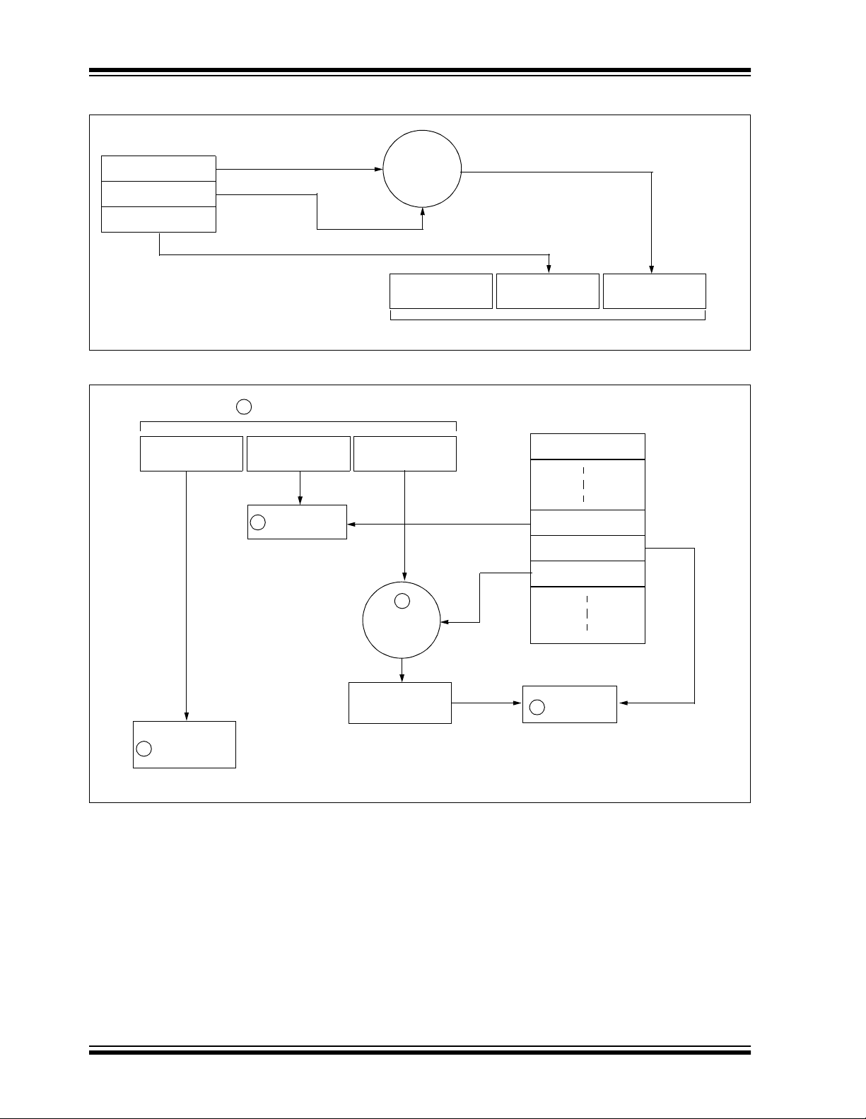
The crypt key generatio n typically input s the transmitter
serial number and 64-bit manufact urer ’s code into t he
key generation algorithm (Figure 1-1). The manufacturer’s code is chosen by the system manufacturer and
must be carefully controlled as it is a pivotal part of the
overall system security.
FIGURE 1-1: CREATION AND STORAGE OF CRYPT KEY DURING PRODUCTION
Production
Programmer
Manufacturer’s
Code
Transmitter
Serial Number
Key
Generation
Algorithm
Crypt
Key
HCS301
EEPROM Array
Serial Number
Crypt Key
Sync Counter
.
.
.
The 16-bit synchronization counter is the basis behind
the transmitted code word changing for each transmission; it increments each time a button is pressed. Due
to the code hoppin g algorith m’s complex ity, each inc rement of the synchronization value results in greater
than 50% of the bits changing in the transmitted code
word.
Figure 1-2 shows how the key values in EEPROM are
used in the encoder . O nce the encoder dete cts a button
press, it reads the button inputs and updates the synchronization counter. The synchronization counter and
crypt key are input to the encryption algorithm and the
output is 32 bits of encrypted information. This data will
change with every button press, its value appearing
externally to ‘ran domly h op aroun d’, hence it is re ferred
to as the hopping portion of the code word. The 32-bit
hopping code is combined with the button information
and serial numb er to fo rm the code word transm itted to
the receiver. The code word format is explained in
greater detail in Section 4.0.
A receiver may use any type of controller as a decoder,
but it is typically a microcon troller with compatible firmware that allows the decoder to operate in conjunction
with an HCS301 based transmitter. Section 7.0
provides detail on integrating the HCS301 into a system.
A transmitter must first be ‘learned’ by the receiver
before its use is allowed in the system. Learning
includes calculating the transmitter’s appropriate crypt
key, decrypting the received hopping code and storing
the serial number, synchronization counter value and
crypt key in EEPROM.
In normal operation, each received message of valid
format is evaluated. The serial number is used to determine if it is from a learned transmitter. If from a learned
transmitter, the message is decrypted and the synchronization counter is verified. Finally, the button status is
checked to see what operation is requested. Figure 1-3
shows the relationship between some of the values
stored by the receiver and the values received from
the transmitter.
2001 Microchip Technology Inc. DS21143B-page 3
Page 4
HCS301
FIGURE 1-2: BUILDING THE TRANSMITTED CODE WORD (ENCODER)
EEPROM Array
Crypt Key
Sync Counter
Serial Number
KEELOQ
Encryption
Algorithm
Button Press
Information
Serial Number
Transmitted Information
FIGURE 1-3: BASIC OPERATION OF RECEIVER (DECODER)
1
Received Information
Button Press
Information
Serial Number
Check for
2
Match
32 Bits of
Encrypted Data
32 Bits
Encrypted Data
EEPROM Array
Manufacturer Code
Serial Number
Sync Counte r
KEELOQ
Decryption
Algorithm
Decrypted
Synchronization
Counter
Perform Function
Indicated by
5
button press
NOTE: Circled numbers indicate the order of execution.
Crypt Key
3
Check for
4
Match
DS21143B-page 4 2001 Microchip Technology Inc.
Page 5
HCS301
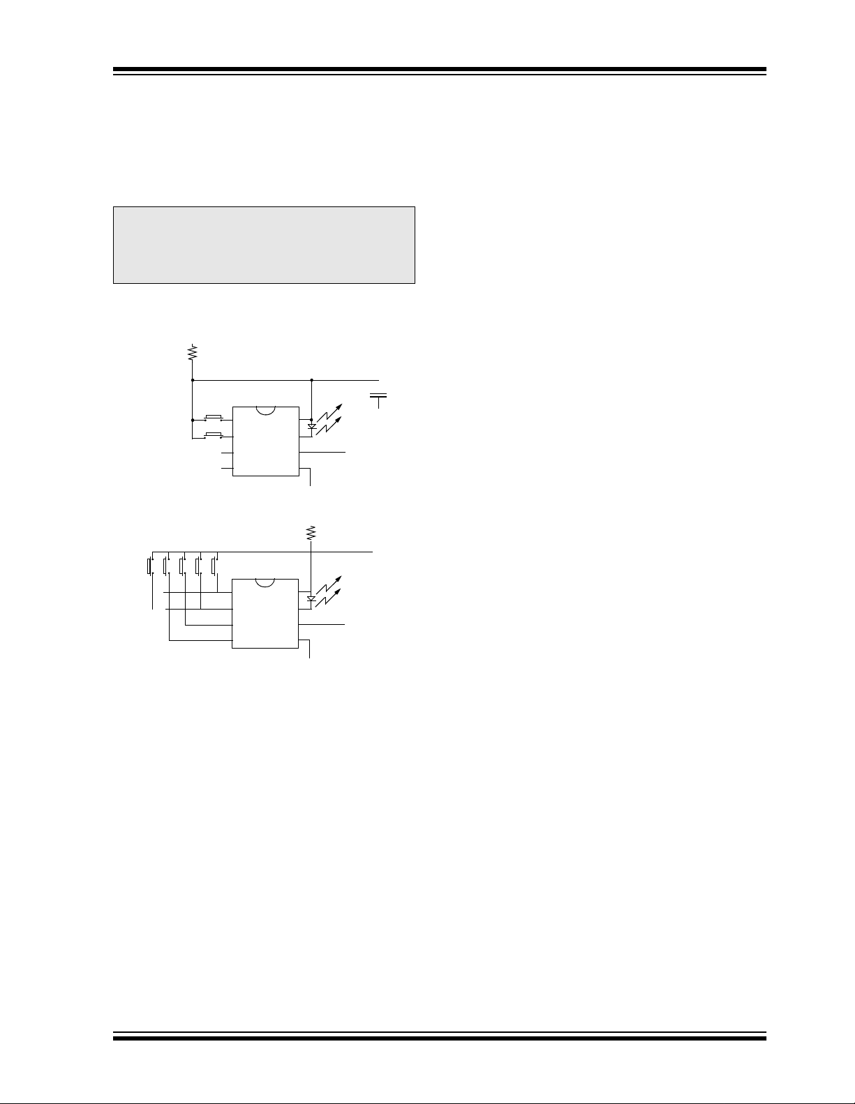
2.0 DEVICE OPERATION
As shown in the typical a pplication circ uits (Figu re 2-1),
the HCS301 is a simple device to use. It requires only
the addition of buttons and RF circuitry for use as the
transmitter in your security applic ation. A descripti on of
each pin is given in Table 2-1.
Note: When VDD > 9.0V and driving low capaci-
tive loads, a res ist or wi th a minimum value
of 50Ω should be used in line with V
This prevents clamping of PWM at 9.0V in
the event of P WM overshoot .
FIGURE 2-1: TYPICAL CIRCUITS
+12V
R
B0
B1
2 button remote control
B4 B3 B2 B1 B0
5 button remote control
Note 1: Up to 15 functions can be implemented by pressing
more than one button si multaneously or by usi ng a
suitable diode array.
2: Resistor R is recommended for current limiting.
S0
S1
S2
S3
S0
S1
S2
S3
(1)
V
DD
LED
PWM
SS
V
DD
V
LED
PWM
V
SS
Tx out
Tx out
DD.
TABLE 2-1: PIN DESCRIPTIONS
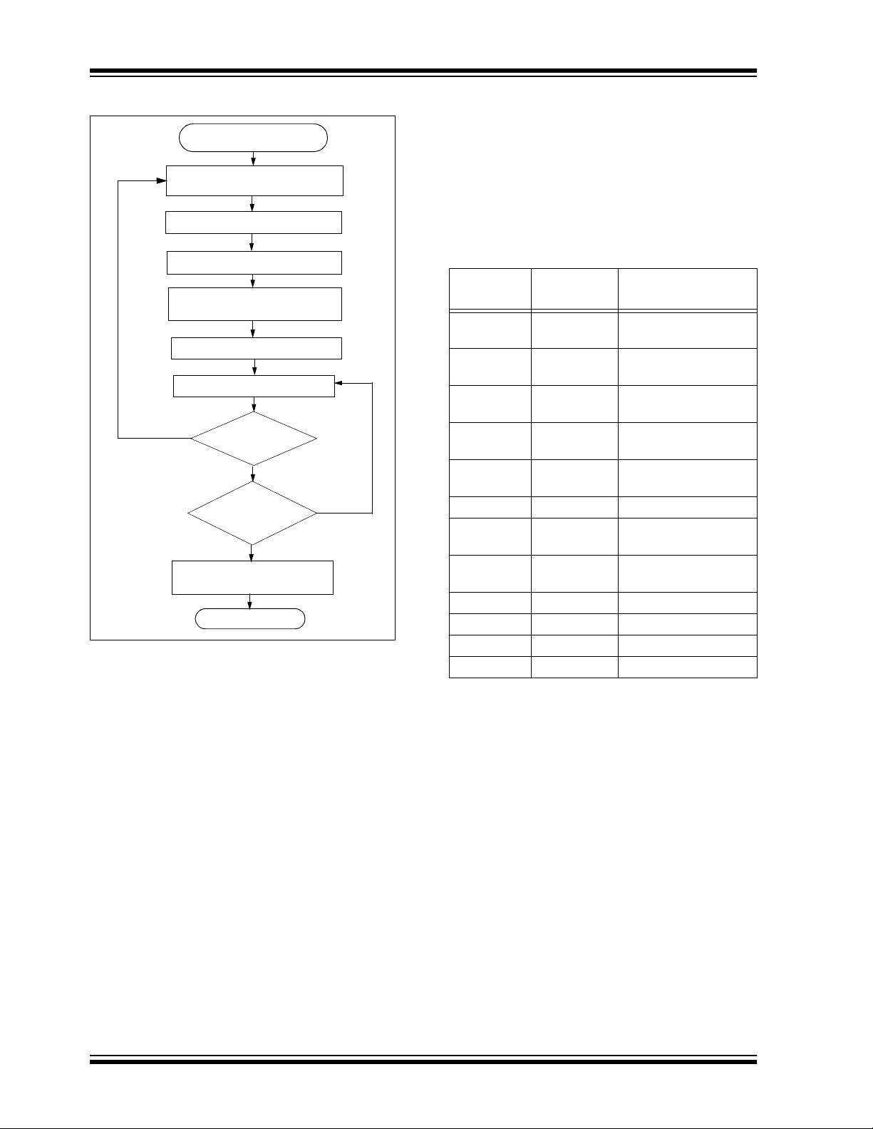
The HCS301 will wake-up upon detecting a button
press and delay approximately 10 ms for button
debounce (Figure 2-2). The synchronization counter,
discrimination value and button information will be
encrypted to form the hopping code. The hopping code
portion will change every transmission, even if the
same button is pushed again. A code word that has
been transmitted will not repeat for more than 64K
transmissions. Thi s provides mo re than 18 years of use
before a code is repeated; based on 10 operations per
day . Overflow inform ation sent from the enc oder can be
used to extend the number of unique transmissions to
more than 192K.
If in the tr an smit proc ess it i s de tec ted t hat a n ew b utton(s) has been pressed, a RESET will immediately
occur and the current cod e word will no t be compl eted.
Please note that buttons removed will not have any
effect on the code word unless no buttons remain
pressed; in which c ase the code word will be compl eted
and the power-down will occur.
2001 Microchip Technology Inc. DS21143B-page 5
Page 6
HCS301
FIGURE 2-2: ENCODER OPERATION
Power-Up
(A button has been pressed)
RESET and Debounce Delay
(10 ms)
Sample Inputs
Update Sync Info
Encrypt With
Crypt Key
Load Transmit Register
Transmit
Yes
Buttons
Added
?
No
All
Buttons
Released
?
Yes
Complete Code
Word Transmission
Stop
No
3.0 EEPROM MEMORY ORGANIZATION
The HCS301 contains 192 bits (12 x 16-bit words) of
EEPROM memory (Table 3-1). This EEPROM array is
used to store the encryption key information,
synchroniz ation v alue, etc. Fur ther de scripti ons of the
memory array is given in the following sections.
T ABLE 3-1: EEPROM MEMORY MAP
WORD
ADDRESS
0 KEY_0 64-bit encryption key
1 KEY_1 64-bit encryption key
2 KEY_2 64-bit encryption key
3 KEY_3 64-bit encryption key
4 SYNC 16-bit synchronization
5 RESERVED Set to 0000H
6 SER_0 Device Serial Number
7 SER_1(Note) Device Serial Number
8 SEED_0 Seed V al ue (word 0)
9 SEED_1 Seed V al ue (word 1)
10 RESERVED Set to 0000H
11 CONFIG Config Word
Note: The MSB of the serial nu mber con tains a bit
MNEMONIC DESCRIPTION
(word 0) LSb’s
(word 1)
(word 2)
(word 3) MSb’s
value
(word 0) LSb’s
(word 1) MSb’s
used to select the Auto-shutoff timer.
3.1 KEY_0 - KEY_3 (64-Bit Crypt Key)
The 64-bit crypt key is used to create the encrypted
message tra nsmitted to the receiver. This ke y is calculated and programmed during production using a key
generation algorithm. The key generation algorithm
may be different from the K
the key generation algorithm are typically the transmit-
ter’s serial numbe r and the 64-bit man ufactu rer’s cod e.
While the key generation algorithm supplied from
Microchip is the typical method used, a user may elect
to create their ow n method of key g eneration. This ma y
be done providing that the deco der is program med with
the same means of creating the key for
decryption purposes.
DS21143B-page 6 2001 Microchip Technology Inc.
EELOQ
algorithm. Inputs to
Page 7

HCS301
3.2 SYNC (Synchronization Counter)
This is the 16-bit synchronization value that is used to
create the hopping code for transmission. This value
will increment after every transmission.
3.3 Reserved
Must be initialized to 0000H.
3.4 SER_0, SER_1
(Encoder Serial Number)
SER_0 and SER_1 are the lower and upper words of
the device serial number, respectively. Although there
are 32 bits allocated for the serial number, only the
lower order 28 bits are transmitted. The serial number
is meant to be unique for every transmitter.
3.4.1 AUTO-SHUTOFF TIMER ENABLE
The Most Sign ificant bit of the serial number (Bit 31) is
used to turn the Auto-shutoff timer on or off. This timer
prevents the transmitter from draining the battery
should a bu tton get stuck in the on positi on for a l ong
period of time. The time period is approximately
25 seconds, after which the device will go to the Timeout mode. When in the Time-out mo de, t he devi ce w ill
stop transmitting, although since some circuits within
the device a re still acti ve, the curre nt draw within the
Shutoff mode will be higher than Standby mode. If the
Most Signifi can t bi t i n the s eri al n umb er i s a o ne, t hen
the Auto-shutoff timer is enabled, and a zero in the
Most Significant bit will disable the timer. The length of
the timer is not selectable.
3.5 SEED_0, SEED_1 (Seed Word)
The 2-word (32-bit) seed c ode will be tr ansmitte d when
all three buttons are pressed at the same time (see
Figure 4-2). This allows the system designer to implement the secu re learn feature or u se this fixed code
word as part of a different key generation/tracking process.
3.6 CONFIG (Configuration Word)
The Configuration Word is a 16-bit word stored in
EEPROM array that is used by the device to store
information used duri ng the encryp tion process, as w ell
as the status of option configurations. The following
sections further explain these bits.
TABLE 3-2: CONFIGURATION WORD
Bit Number Bit Description
0 Discrimination Bit 0
1 Discrimination Bit 1
2 Discrimination Bit 2
3 Discrimination Bit 3
4 Discrimination Bit 4
5 Discrimination Bit 5
6 Discrimination Bit 6
7 Discrimination Bit 7
8 Discrimination Bit 8
9 Discrimination Bit 9
10 Overflow Bit 0 (OVR0)
11 Overflow Bit 1 (OVR1)
12 Low Voltage Trip Poi nt Select
(V
LOW SEL)
13 Baud rate Select Bit 0 (BSL0)
14 Baud rate Select Bit 1 (BSL1)
15 Reserved, set to 0
3.6.1 DISCRIMINATION VALUE
(DISC0 TO DISC9)
The discrimination value aids the post-decryption
check on the decoder end. It may be any value, but in
a typical system it will be programmed as the 10 Least
Significant bits of the serial number. Values other than
this must be separately stored by the receiver when a
transmitter is learned. The discrimination bits are part
of the information tha t form the encrypte d portion o f the
transmission (Figure 4-2). After the receiver has
decrypted a transmission, the discrimination bits are
checked against the receiver’s stored value to verify
that the decryption proc ess was v alid. If the discrim ination value was programmed as the 10 LSb’s of the
serial number then it may merely be compared to the
respectiv e bits of the received se rial number; saving
EEPROM space.
3.6.2 OVERFLOW BITS
(OVR0, OVR1)
The overflow bits are used to extend the number of
possible synchronization values. The synchronization
counter is 16 bits in length, yielding 65,536 values
before the cycle repeats. Under typical use of
10 operations a day , th is will provi de nea rly 18 year s of
use before a repeated value will be used. Should the
system designer conclude that is not adequate, then
the overflow bits can be utilized to extend the number
2001 Microchip Technology Inc. DS21143B-page 7
Page 8

HCS301
of unique values. This can be done by programming
OVR0 and OVR1 to 1s at the time of production. The
encoder will automatica lly clear OVR0 the first time that
the synchronization value wraps from 0xFFFF to
0x0000 and clear OVR1 the second time the counter
wraps. Once cleared, OVR0 and OVR1 cannot be set
again, thereby creating a permanent record of the
counter overflow. This prevents fast cycling of 64K
counter. If the decoder system is programmed to track
the overflow bits, then the effective number of unique
synchronization values can be extended to 196,608.
3.6.3 BAUD RATE SELECT BITS
(BSL0, BSL1)
BSL0 and BSL1 select the speed of transmission and
the code word blanking. Table 3-3 shows how the bits
are used to select the different baud rates and
Section 5.7 provides detailed explanation in code word
blanking.
TABLE 3-3: BAUD RATE SELECT
BSL1 BSL0
Basic Pulse
Element
0 0 400 µsAll
0 1 200 µs 1 out of 2
1 0 100 µs 1 out of 2
1 1 100 µs 1 out of 4
Code Words
Transmitted
3.6.4 LOW VOLTAGE TRIP POINT
SELECT
The low voltage trip point select bit is used to tell the
HCS301 what
VDD level is being used. This information
will be used by the device to determine when to send the
voltage low signal to the receiver. When this bit is set to
a one, the
9V or 12V
VDD level is assumed to be operating from a
VDD level. If the bit is set low, then the VDD le vel
is assumed to be 6.0 volts. Refer to Figure 3-1 for voltage trip point.
FIGURE 3-1: VOLTAGE TRIP POINTS
BY CHARACTERIZATION
Volts (V)
5.5
5.0
4.5
4.0
3.5
3.0
2.5
9.0
8.5
8.0
7.5
7.0
VLOW sel = 0
VLOW sel = 1
V
LOW
Max
Min
Max
Min
-40 20 40 100
-20 0 60 80
Temp (C)
DS21143B-page 8 2001 Microchip Technology Inc.
Page 9
HCS301
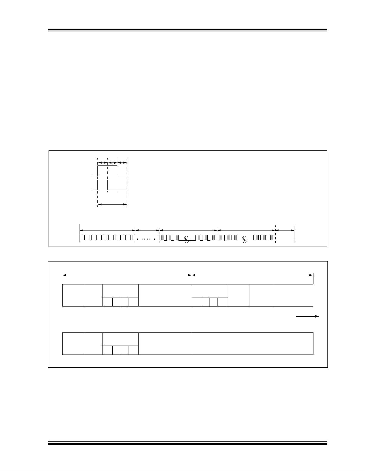
4.0 TRANSMITTED WORD
4.1 Code Word Format
The HCS301 code word is made up of several parts
(Figure 4-1). Each code word contains a 50% duty
cycle preamble, a hea der , 32 bits of en crypted data an d
34 bits of fixed data followed by a guard period before
another code word can begin. Refer to Table 8-4 for
code word timing.
FIGURE 4-1: CODE WORD FORMAT
TE
TE
TE
LOGIC ‘0’
LOGIC ‘1’
Bit
Period
50% Duty Cycle
Preamble
TP
Header
TH
Encrypted Portion
of Transmission
4.2 Code Word Organization
The HCS301 transmits a 66-bit code word when a
button is pressed. The 66-bit word is constructed from
a Fixed Code portion and an Encrypted Code portion
(Figure 4-2).
The 32 bits of Encrypted Data are generated from 4
button bits, 12 discrimination bits and the 16-bit sync
value. The encrypted portion alone provides up to four
billion changing code combinations.
The 34 bits of Fixed Code Data are made up of 2 status bits, 4 button bits and the 28-bit serial number. The
fixed and encrypted sections combined increase the
number of code combinations to 7.38x 10
THOP
Fixed Portion of
Transmission
TFIX
Guard
Time
TG
19
.
FIGURE 4-2: CODE WORD ORGANIZATION
34 bits of Fixe d Portion 32 bits of Encrypted Por tion
Button
Status
S2 S1 S0 S3
Button
Status
1 1 1 1
Serial Number
(28 bits)
Serial Number
(28 bits)
MSb
MSb
Repeat
(1 bit)
Repeat
(1 bit)
VLOW
(1 bit)
LOW
V
(1 bit)
Note: SEED replaces Encrypted Portion when all button inputs are activated at the same time.
Button
Status
S2 S1 S0 S3
OVR
(2 bits)
DISC
(10 bits)
SEED
(32 bits)
Sync Counter
(16 bits)
66 Data bits
Transmitted
LSb first.
LSb
LSb
2001 Microchip Technology Inc. DS21143B-page 9
Page 10

HCS301
4.3 Synchronous T ransmi ssion Mode
Synchronous T ran smis sion mode can b e used t o cl ock
the code word out using an external clock.
To enter Synchronous Transmission mode, the Programming mode start-up sequence must be executed
as shown in Figure 4-3. If either S1 or S0 is set on the
falling edge of S2 (or S3), the device enters Synchronous Transmissio n mo de. In th is mo de, it fu ncti ons as
a normal transmitter, with the exception that the timing
of the PWM data string is cont rol led ext ernal ly and 16
extra bits are transm itted at the end with the code word.
The button code will be the S0, S1 value at the falling
edge of S2 or S3. The timing of th e PWM da ta string is
controlled by sup plyin g a cl ock o n S2 or S3 and sh ould
not exceed 20 kHz. The code word is the same as in
PWM mode with 16 reserved bits at the end of the
word. The reserved bits can be ignored. When in Synchronous Transmission mode S2 or S3 should not be
toggled until all internal processing has been completed as shown in Figure 4-4.
FIGURE 4-3: SYNCHRONOUS TRANSMISSION MODE
TPS
PWM
S2
S[1:0]
TPH1
TPH2
“01,10,11”
t = 50ms
Preamble
Header
Data
FIGURE 4-4: CODE WORD ORGANIZATION (SYNCHRONOUS TRANSMISSION MODE)
Fixed Portion Encrypted Portion
MSb
Reserved
(16 bits)
Padding
(2 bits)
Button
Status
S2 S1 S0 S3
Serial Number
(28 bits)
Button
Status
S2 S1 S0 S3
DISC+ OVR
(12 bits)
82 Data bits
Transmitted
LSb first.
Sync Counter
(16 bits)
LSb
DS21143B-page 10 2001 Microchip Technology Inc.
Page 11

HCS301
5.0 SPECIAL FEATURES
5.1 Code Word Completion
The code word completion feature ensures that entire
code words are transmitted, even if the button is
released before the code word is complete. If the button is held down beyond the time for one code word,
multiple code words will result. If another button is activated during a transmission, the active transmission
will be aborted an d a ne w tran smis sion will be gin u sing
the new button information.
5.2 LED Output Operation
During normal transmission the LED output is LO W. If
the supply voltage drops below the low voltage trip
point, the LED output will be toggl ed at appr oximate ly
5Hz during the transmission (Section 3.6.4).
5.3 RPT: Repeat Indicator
This bit will be low for the first transmitted word. If a
button is held down for more than one transmitted cod e
word, this bit will be set to indicate a repeated code
word and remain set until the button is released.
5.4 VLOW: Voltage LOW Indicator
5.6 Seed Trans mission
In order to i nc rea se t h e l e vel o f se c ur it y i n a s ys t em , i t
is possible for the receiver to implement what is known
as a secure l earn functio n. This c an be done by utiliz ing
the seed value stored in EEPROM, transmitted only
when all three button inputs are pressed at the same
time (Table5-1). Instead of the normal key generation
inputs being used to create the crypt key, this seed
value is used.
TABLE 5-1: PIN ACTIVATION TABLE
Function S3 S2 S1 S0
Standby 0
Hopping Code
Seed Code 15
1
2
13
14
000 0
000 1
001 0
--- 110 1
111 0
111 1
The VLOW signal is transmitted so the receiver can giv e
an indication to the user that the transmitter battery is
low. The VLOW bit is included in every transmission
(Figure 4-2 and Figure 8-5) and will be transmitted as a
zero if the operating voltage is above the low voltage
trip point. Refer to Figure4-2. The trip point is selectable based on the b attery voltage being used. See Se ction 3.6.3 for a description of how the low voltage trip
point is configured.
5.5 Auto-shutoff
The Auto-shutoff function automatically stops the
device from transmitting if a button inadvertently gets
pressed fo r a lo ng p eri od of tim e. Th is w ill prev ent the
device from draining the battery if a button gets
pressed whil e the transmitte r is in a pocket or purse .
This function can be enabled or disabled and is
selected by setting or clearing the Auto-shutoff bit (see
Section 3.4.1). Setting this bit hi gh will enable the function (turn Auto-shutoff function on) and setting the bit
low will disable th e func tion. Time-out pe riod is appro ximately 25 seconds.
2001 Microchip Technology Inc. DS21143B-page 11
Page 12

HCS301
5.7 Blank Alternate Code Word
Federal Communications Commission (FCC) part 15
rules specify the limits on worst case av erage fundamental power and harmonics that can be transmitted in
a 100 ms window. For FCC a ppro val pur pos es, it may
therefore be advantageous to minimize the transmission duty cycle. This ca n be achieved by minim izing the
duty cycle of the individual bits as well as by blanking
out consecutive code words. Blank Alternate Code
Word (BACW) may be used to reduce the average
power of a transmi ssion by tra nsmittin g only ev ery sec-
ond code word (Figure 5-1). This is a selectable feature
that is determined in conjunction with the baud rate
selection bit BSL0.
Enabling the BACW optio n may lik ewise a llow the user
to transmit a higher am plitud e transmis sion as the tim e
averaged power is reduced. BACW effectively halves
the RF on time for a given transmission so the RF output power could theoretically be doubled while maintaining the same time averaged output power.
FIGURE 5-1: BLANK ALTERNATE CODE WORD (BACW)
Amplitude
BACW Disabled
(All words transmitted)
BACW Enabled
(1 out of 2 transmitted)
BACW Enabled
(1 out of 4 transmitted)
A
2A
4A
Code Word
Code Word Code Word Code Word
Time
DS21143B-page 12 2001 Microchip Technology Inc.
Page 13

HCS301
6.0 PROGRAMMING THE HCS301
When using the HCS301 in a s ystem, the user will have
to program some parameters into the device including
the serial number and the secret key before it can be
used. The programming cycle allows the user to input
all 192 bits in a serial data stream, which are then
stored internally in EEPROM. Programming will be
initiated by forcing the PWM line high, after the S2 (or
S3) line has been held high for the appropriate length
of time line (Table 6-1 and Figure 6-1). After the Program mode is entered, a d elay mu st be prov ided to the
device for t he automatic bulk write cyc le to compl ete.
This will set all locations in th e EEPROM to zeros. Th e
device can then be programmed by clocking in 16 bits
at a time, using S2 (or S3) as the clock line and PWM
as the data in line. After each 16-bit word is loaded, a
FIGURE 6-1: PROGRAMMING WAVEFORMS
S2 (S3)
(Clock)
PWM
(Data)
Enter Program
Mode
TPS
TPH1
TPBW
TCLKH
TCLKL
Bit 0 Bit 1 Bit 2 Bit 3 Bit 14 Bit 15 Bit 16 Bit 17
TDS
TDH
programming delay is requir ed for the internal pro gram
cycle to complet e. This delay can t ake up to T
end of the programming cycle, the device can be verified (Figure 6-2) by reading back the EEPROM. Reading is done by clocking the S2 (or S3) line and reading
the data bits on PWM . For security reaso ns, it is not
possible to execute a verify function without first programming the EEPROM. A Verify operation c an on ly
be done once, immediately following the Program
cycle.
Note: To ensure that the device does not acci-
dentally enter Programming mode, PWM
should never be pulled high by the circuit
connected to it. Special care should be
taken when driving PNP RF transistors.
TWC
WC. At the
TPH2
Note 1: Unused button inputs to be held to ground during the entire programming sequence.
2: The VDD pin must be taken to ground after a Program/Verify cycle.
Data for Word 0 (KEY_0)
Repeat for each word (12 times)
FIGURE 6-2: VERIFY WAVEFORMS
End of Programming Cycle Beginning of Verify Cycle
PWM
(Data)
S2 (S3)
(Clock)
Note: If a Verify operation is to be done, then it must immediately follow the Program cycle.
Data from Word 0
Bit 0Bit191Bit190
TWC
Bit 1 Bit 2 Bit 3 Bit 15Bit 14 Bit 16 Bit 17 Bit190 Bit191
TDV
Data for Word 1
2001 Microchip Technology Inc. DS21143B-page 13
Page 14

HCS301
TABLE 6-1: PROGRAMMING/VERIFY TIMING REQUIREMENTS
VDD = 5.0V ± 10%, 25 °C ± 5 °C
Parameter Symbol Min. Max. Units
Program mode setup time
Hold time 1
Hold time 2
Bulk Write time
Program delay time
Program cycle time
Clock low time
Clock high time
Data setup time
Data hold time
Data out valid time
Note 1: Typical values - not tested in production.
TPS 3.5 4.5 ms
PH1 3.5 —ms
T
PH2 50 — µs
T
PBW 4.0 — ms
T
T
PROG 4.0 — ms
T
WC 50 — ms
TCLKL 50 — µs
CLKH 50 — µs
T
DS 0—
T
DH 30 —
T
TDV —30
µs
µs
µs
(1)
(1)
(1)
DS21143B-page 14 2001 Microchip Technology Inc.
Page 15

HCS301
7.0 INTEGRATING THE HCS301 INTO A SYSTEM
Use of the HCS301 in a system requires a compatible
decoder . This decoder is typically a microco ntroller with
compatible firmware. Microchip will provide (via a
license agreement) firmware routines that accept
transmissions from the HCS301 and decrypt the
hopping code portion of the data stream. These
routines provide system designers the means to
develop their own decoding system.
7.1 Learning a Transmitter to a
Receiver
A transmitter must first be ’ learned’ by a decoder before
its use is allowed in the system. Several learning strategies are possible, Figure 7-1 details a typical learn
sequence. Core to each, the decoder must minimally
store each learned trans mitter’ s seri al nu mber and c urrent synchronization counter value in EEPROM. Additionally, the decoder typically stores each transmitter’s
unique crypt key. The maximum number of learned
transmitters will therefore be relative to the available
EEPROM.
A transmitter’s serial number is transmitted in the clear
but the synchronization counter only exists in the code
word’s encrypted portion. The decoder obtains the
counter value by decrypting using the same key used
to encrypt the information. The K
symmetrical block cipher so the e ncryption and decryption keys are identical and referred to generally as the
crypt key. The encoder receives its crypt key during
manufacturing. The decoder is programmed with the
ability to generate a crypt key as well as all but one
required input to the key generation routine; typically
the transmitter’s serial number.
Figure 7-1 summarizes a typical learn sequence. The
decoder receives and authenticates a first transmission; first button press. Authentication involves generating the ap propriate crypt ke y, decrypting, v alidating
the correct key usage via the discrimination bits and
buffering th e counter v alue. A seco nd transmi ssion is
received and authenticated. A final check verifies the
counter values were sequential; consecutive button
presses. If the learn sequence is successfully complete, the decoder stores the learned transmitter’s
serial number, current synchronization counter value
and appropriate crypt key. From now on the crypt key
will be retrieved from EEPROM during normal operation instead of recalculating it for each transmission
received.
Certain learning strategies have been patented and
care must be taken not to infringe.
EELOQ algorithm is a
FIGURE 7-1: TYPICAL LEARN
SEQUENCE
Enter Learn
Mode
Wait for Reception
of a Valid Code
Generate Key
from Serial Number
Use Generated Key
to Decrypt
Compare Discrimination
2001 Microchip Technology Inc. DS21143B-page 15
Page 16

HCS301
Page 17
FIGURE 7-3: SYNCHRONIZATION WINDOW
Entire Window
rotates to eliminate
use of previously
used codes
Blocked
Window
(32K Codes)
Double Operation
(resynchronization )
Window
(32K Codes)
HCS301
Stored
Synchronization
Counter Value
Single Operation
Window
(16 Codes)
2001 Microchip Technology Inc. DS21143B-page 17
Page 18

HCS301
8.0 ELECTRICAL CHARACTERISTICS
TABLE 8-1: ABSOLUTE MAXIMUM RATINGS
Symbol Item Rating Units
VDD Supply voltage -0.3 to 13.3 V
V
IN Input voltage -0.3 to 13.3 V
VOUT Output voltage -0.3 to VDD + 0.3 V
I
OUT Max output current 25 mA
T
STG Storage temperature -55 to +125 °C (Note)
TLSOL Lead soldering temp 300 °C (Note)
V
ESD ESD rating 4000 V
Note: Stresses above those listed under “ABSOLUTE MAXIMUM RATINGS” may cause permanent damage to
the device.
TABLE 8-2: DC CHARACTERISTICS
Commercial(C): Tamb = 0 °C to +70 °C
Industrial (I): Tamb = -40 °C to +85 °C
3.5V < VDD < 13.0V
Parameter Sym. Min Typ* Max Unit Conditions
Operating current (avg) I
Standby current I
High level Input voltage V
CC 0.6
1.5
8.0
CCS 110µA
IH 0.4 VDD VDD+
1.0
3.0
12.0
mA
V
0.3
Low level input voltage VIL -0.3 0.15 VDD V
High level output voltage V
Low level output voltage V
sink current ILED 3.5
LED
Pull-down Resist anc e;
OH 0.5 VDD VIOH = -2 mA
OL 0.08 VDD VIOL = 2 mA
4.7
2.7
S0-3 40 60 80
R
3.7
5.9
4.6
mA VDD = 6.6V, VLOW source = 0
kΩ
S0-S3
Pull-down Resist anc e;
R
PWM 80 120 160
kΩ
PWM
Note: Typical values are at 25 °C.
VDD = 3.5V
V
DD = 6.6V
DD = 13.0V
V
(Figure 8-1)
DD = 13.0V, VLOW source = 1
V
VIN = 4.0V
VIN = 4.0V
DS21143B-page 18 2001 Microchip Technology Inc.
Page 19

FIGURE 8-1: TYPICAL ICC CURVE OF HCS301 WITH EXTERNAL RESISTORS
50Ω External
12.0
10.0
8.0
6.0
mA
4.0
2.0
0.0
23456789 1112
VBAT [V]
1 κΩ External
12.0
10
HCS301
13
mA
mA
10.0
8.0
6.0
4.0
2.0
0.0
23456789 11121310
VBAT [V]
2 κΩ External
12.0
10.0
8.0
6.0
4.0
2.0
0.0
23456789 11121310
VBAT [V]
LEGEND
Typical
Maximum
Minimum
2001 Microchip Technology Inc. DS21143B-page 19
Page 20

HCS301
FIGURE 8-2: POWER-UP AND TRANSMIT TIMING
Button Press
PWM
Output
Button
Input
Sn
Detect
BP
T
TTD
T
DB
Code
Word
1
Multiple Code Word Transmission
TTO
Code
Word
2
Code
Word
3
Code
Word
4
Code
Word
n
TABLE 8-3: POWER-UP AND TRANSMIT TIMING
VDD = +3.5 to 13.0V
Commercial(C): Tamb = 0°C to +70°C
Industrial(I): Tamb = -40°C to +85°C
Symbol Parameter Min Max Unit Remarks
TBP Time to second button press 10 + Code
TD Transmit delay from button det ect 10 26 ms
T
TDB Debounce Delay 6 15 ms
T
TO Auto-shutoff time-out period 20 120 s
Note 1: TBP is the time in w hich a sec ond b utton c an b e pr esse d witho ut co mpleti on of th e first code word a nd the
intention was to press the combination of buttons.
2: Typical values - not tested in production.
(2)
Word
26 + Code
Word
ms (Note 1)
FIGURE 8-3: CODE WORD FORMAT
TE
TE
TE
Bit Period
T
BP
LOGIC ‘0’
LOGIC ‘1’
50% Duty Cycle
Preamble
TP
DS21143B-page 20 2001 Microchip Technology Inc.
Header
TH
Encrypted Portion
of Transmission
THOP
Fixed Portion of
Trans mission
TFIX
Guard
Time
TG
Page 21

FIGURE 8-4: CODE WORD FORMAT: PREAMBLE/HEADER PORTION
HCS301
P1
50% Duty Cycle Preamble Header
23 TE 10 TE Data Bits
P12
FIGURE 8-5: CODE WORD FORMAT: DATA PORTION
Serial Number Button Code Status
LSB
MSB MSB S3 S0 S1 S2 VLOW RPT
Bit 30
Bit 31
Bit 32 Bit 33 Bit 58 Bit 59
Bit 60
Bit 61
Fixed Portion
Bit 62 Bit 63Bit 64 Bit 65
Header
LSB
Bit 0 Bit 1
Encrypted Portion
TABLE 8-4: CODE WORD TRANSMISSION TIMING REQUIREMENTS
VDD = +2.0 to 6.0V
Commercial(C):Tamb = 0 °C to +70 °C
Industrial(I):Tamb = -40 °C to +85 °C
Symbol Characteristic
Number
E
of T
All 1 out of 2 1 out of 4
Min. Typ. Max. Min. Typ. Max. Min. Typ. Max. Units
Code Words Transmitted
Bit 0 Bit 1
Guard
Time
T
TBP
TP
TH
THOP
TFIX
TG
—
—
Note: The timing parameters are not tested but derived from the oscillator clock.
Basic pulse element
E
PWM bit pulse width
Preamble duration
Header duration
Hopping code duration
Fixed code duration
Guard Time
Total Transmit Time
PWM data rate
1 260 400 660 130 200 330 65 100 165 µs
3 780 1200 1980 390 600 990 195 300 495 µs
23 6.0 9.2 15.2 3.0 4.6 7.6 1.5 2.3 3.8 ms
10 2.6 4.0 6.6 1.3 2.0 3.3 0.7 1.0 1.7 ms
96 25.0 38.4 63.4 12.5 19.2 31.7 6.2 9.6 15.8 ms
102 26.5 40.8 67.3 13.3 20.4 33.7 6.6 10.2 16.8 ms
39 10.1 15.6 25.7 5.1 7.8 12.9 2.5 3.9 6.4 ms
270 70.2 108.0 178.2 35.1 54.0 89.1 17.6 27.0 44.6 ms
— 1282 833 505 2564 1667 1010 5128 3333 2020 bps
2001 Microchip Technology Inc. DS21143B-page 21
Page 22

HCS301
FIGURE 8-6: HCS301 TE VS. TEMP (BY CHARACTERIZATION ONLY)
1.7
1.6
1.5
1.4
1.3
1.2
E
T
1.1
1.0
0.9
0.8
0.7
0.6
-50 -40 -30 -20 -10 0 10 20 30 40 50 60 70 80 90
TE MAX.
VDD = 3.5V
VDD = 5.0V
TE MAX.
VDD = 5.0V
Typical
VDD = 5.0V
TE Min.
TEMPERATURE
DS21143B-page 22 2001 Microchip Technology Inc.
Page 23

9.0 PACKAGING INFORMATION
9.1 Package Marking Information
8-Lead PDIP (300 mil) Example
HCS301
XXXXXXXX
XXXXXNNN
HCS301
XXXXXNNN
YYWW
8-Lead SOIC (150 mil) Example
XXXXXXX
XXXYYWW
HCS301
XXX0025
NNN
Legend: XX...X Customer specific information*
Y Year code (last digit of calendar year)
YY Year code (last 2 digits of calendar year)
WW Week code (week of January 1 is week ‘01’)
NNN Alphanumeric traceability code
0025
NNN
Note: In the event the full Micro chip p art num ber can not be ma rked on one line, it will
be carried over to the next l ine thus lim it ing t he nu mb er of av ai lab le cha r ac ters
for customer specific information.
* Standard PICmicro device marking consists of Microchip part number, year code, week code, and
traceability code. For PICmicro device marking beyond this, certain price adders apply. Please check
with your Microchip Sales Office. For QTP devices, any special marking adders are included in QTP
price.
2001 Microchip Technology Inc. DS21143B-page 23
Page 24
HCS301
9.2 Package Details
8-Lead Plastic Dual In-line (P) - 300 mil (PDIP)
E1
2
D
n
E
β
eB
Number of Pins
Pitch
Top to Seating Plane A .140 .155 .170 3.56 3.94 4.32
Molded Package Thickness A2 .115 .130 .145 2.92 3.30 3.68
Base to Seating Plane A1 .015 0.38
Shoulder to Shoulder Width E .300 .313 .325 7.62 7.94 8.26
Molded Package Width E1 .240 .250 .260 6.10 6.35 6.60
Overall Length D .360 .373 .385 9.14 9.46 9.78
Tip to Seating Plane L .125 .130 .135 3.18 3.30 3.43
Lead Thickness
Upper Lead Width B1 .045 .058 .070 1.14 1.46 1.78
Lower Lead Width B .014 .018 .022 0.36 0.46 0.56
Overall Row Spacing § eB .310 .370 .430 7.87 9.40 10.92
Mold Draft Angle Top
Mold Draft Angle Bottom
* Controlling Parameter
§ Significant Characteristic
Notes:
Dimensions D and E1 do not include mold flash or protrusions. Mold flash or protrusions shall not exceed
.010” (0.254mm) per side.
JEDEC Equivalent: MS-001
Drawing No. C04-018
Dimension L imits MIN NOM MAX MIN NOM MAX
1
α
A
c
Units INCHES* MILLIMETERS
n
p
c
α
β
.008 .012 .015 0.20 0.29 0.38
A1
B1
B
88
.100 2.54
51015 51015
51015 51015
A2
L
p
DS21143B-page 24 2001 Microchip Technology Inc.
Page 25

8-Lead Plastic Small Outline (SN) - Narrow, 150 mil (SOIC)
E
E1
p
D
2
HCS301
B
Number of Pins
Pitch
Foot Angle
Lead Thickness
Mold Draft Angle Top
Mold Draft Angle Bottom
n
°
45
c
β
1
h
φ
L
MILLIMETERSINCHES*Units
n
p
φ
c
α
β
048048
MAXNOMMINMAXNOMMINDimension Limits
88
1.27.050
1.751.551.35.069.061.053AOverall Height
1.551.421.32.061.056.052A2Molded Package Thickness
0.250.180.10.010.007.004A1Standoff §
6.206.025.79.244.237.228EOverall Width
3.993.913.71.157.154.146E1Molded Package Width
5.004.904.80.197.193.189DOverall Length
0.510.380.25.020.015.010hChamfer Distance
0.760.620.48.030.025.019LFoot Length
0.250.230.20.010.009.008
0.510.420.33.020.017.013BLead Width
1512015120
1512015120
2001 Microchip Technology Inc. DS21143B-page 25
Page 26

HCS301
ON-LINE SUPPORT
Microchip provides on-line support on the Microchip
World Wide Web (WWW) site.
The web site is used b y Micr ochip as a means to mak e
files and information easily available to customers. To
view the site, the use r must hav e access to the Intern et
and a web browser, such as Netscape or Microsoft
Explorer. Files are also available for FTP download
from our FTP site.
Connecting to the Microchip Internet Web Site
The Microchip web site is available by using your
favorite Internet browser to attach to:
www.microchip.com
The file transfer site is available by using an FTP service to connect to:
ftp://ftp.microchip.com
The web site and file transfer site provide a variety of
services. Users may download files for the latest
Development Tools, Data Sheets, Application Notes,
User’s Guides, Articles and Sample Programs. A variety of Micr ochip specific bu siness informati on is also
available, including listings of Microchip sales offices,
distributors and factory representatives. Other data
available for consideration is:
• Latest Microchip Press Releases
• Technical Support Section with Frequently Asked
Questions
• Design Tips
• Device Errata
• Job Postings
• Microchip Consultant Pr ogram Member Listing
• Links to other useful web sites related to
Microchip Products
• Conferences for p roducts, D evelopment Systems,
technical information and more
• Listing of seminars and events
Systems Information and Upgrade Hot Line
The Systems Information and Upgrade Line provides
system users a listing of the latest versions of all of
Microchip's development systems software products.
Plus, this line provides information on how customers
can receive any currently available upgrade kits.The
Hot Line Numbers are:
1-800-755-2345 for U.S. and most of Canada, and
1-480-792-7302 for the rest of the world.
DS21143B-page 26 2001 Microchip Technology Inc.
Page 27

HCS301
READER RESPONSE
It is our intentio n to pro vi de you with the best do cu me nt ation possible to e ns ure suc c ess ful use of your Mic roc hip pro duct. If you wish to prov ide y our co mmen ts on org aniza tion, c larity, subject matter, and ways in which our doc ument atio n
can better serve you, please FAX your comments to the Technical Publications Manager at (480) 792-4150.
Please list the following information, and use this outline to provide us with your comments about this Data Sheet.
To:
RE: Reader Response
From:
Application (optional):
Would you like a reply? Y N
Device:
Questions:
1. What are the best features of this document?
2. How does this document meet your hardware and software development needs?
3. Do you find the organization of this data sheet easy to follow? If not, why?
Technical Publications Manager
Name
Company
Address
City / State / ZIP / Country
Telephone: (_______) _________ - _________
HCS301
Literature Number:
Total Pages Se nt
FAX: (______) _________ - _________
DS21143B
4. What additions to the data sheet do you think would enhance the structure and subject?
5. What deletions from the data sheet could be made without affecting the overall usefulness?
6. Is there any incorrect or misleading information (what and where)?
7. How would you improve this document?
8. How would you improve our software, systems, and silicon products?
2001 Microchip Technology Inc. DS21143B-page 27
Page 28

HCS301
HCS
/P
HCS301 PRODUCT IDENTIFICATION SYSTEM
To order or obtain information, e.g., on pricing or delivery, refer to the factory or the listed sales office.
301 -
Package: P = Plastic DIP (300 mil Body), 8-lead
Temperature Blank = 0°C to +70°C
Range: I = –40°C to +85°C
Device: HCS301
SN = Plastic SOIC (150 mil Body), 8-lead
Code Hopping Encoder
=
HCS301T
Code Hopping Encoder (Tape and Reel)
=
Sales and Support
Data Sheets
Products supported by a preliminary Data Sheet may have an errata sheet describing minor operational differences
and recommended workarounds. To determine if an errata sheet exists for a particular device, please contact one of
the following:
1. Your local Microchip sales office
2. The Microchip Corporate Literature Center U.S. FAX: (480) 792-7277
3. The Microchip Worldwide Site (www.microchip.com)
Please specify which device, revision of silicon and Data Sheet (include Literature #) you are using.
New Customer Notification System
Register on our web site (www.microchip.com/cn) to receive the most current information on our products.
DS21143B-page 28 2001 Microchip Technology Inc.
Page 29

Microchip’s Secure Data Products are covered by some or all of the following patents:
Code hopping encoder patents issued in Europe, U.S.A., and R.S.A. — U.S.A.: 5,517,187; Europe: 0459781; R.S.A.: ZA93/4726
Secure learning patents issued in the U.S.A. and R.S.A. — U.S.A.: 5,686,904; R.S.A.: 95/5429
Information contained in this publication regarding device
applications and the like is intended through suggestion only
and may be superseded by updates. It is your responsibility to
ensure that your application meets with your specifications.
No representation or warranty is given and no liability is
assumed by Microchip Technology Incorporated with respect
to the accuracy or use of such information, or infringement of
patents or other intellectual property rights arising from such
use or otherwise. Use of Microchip’s products as critical components in life support systems is not authorized except with
express written approval by Microchip. No licenses are conveyed, implicitly or otherwise, under any intellectual property
rights.
Trademarks
The Microchip name and logo, the Microchip logo, FilterLab,
K
EELOQ, MPLAB, PIC, PICmicro, PICMASTER, PICSTART,
PRO MATE, SEEVAL and The Embedded Control Solutions
Company are registered trademarks of Microchip Technology
Incorporated in the U.S.A. and other countries.
dsPIC, ECONOMONITOR, FanSense, FlexROM, fuzzyLAB,
In-Circuit Serial Programming, ICSP, ICEPIC, microID,
microPort, Migratable Memory, MPASM, MPLIB, MPLINK,
MPSIM, MXDEV, PICC, PICDEM, PICDEM.net, rfPIC, Select
Mode and Total Endurance are trademarks of Microchip
Technology Incorporated in the U.S . A .
Serialized Quick Turn Programming (SQTP) is a service mark
of Microchip Technology Incorporated in the U.S.A.
All other trademarks mentioned herein are property of their
respective companies.
© 2001, Microchip Technology Incorporated, Printed in the
U.S.A., All Rights Reserved.
Printed on recycled paper.
Microchip received QS-9000 quality system
certification for its worldwid e head qu art ers,
design and wafer fabrication facilities in
Chandler and Tempe, Arizona in July 1999. The
Company’s quality system processes and
procedures are QS-9000 compliant for its
PICmicro
devices, Serial EEPROMs and microperipheral
products. In addition, Microchip’s quality
system for the design and manufacture of
development systems is ISO 9001 certified.
®
8-bit MCUs, KEELOQ
®
code hoppin g
2001 Microchip Technology Inc. DS21143B - page 29
DS21143B-page 30 2001 Microchip Technology Inc.
Page 30

 Loading...