


ENC424J600/624J600
Data Sheet
Stand-Alone 10/100 Ethernet Controller
with SPI or Parallel Interface
2010 Microchip Technology Inc. DS39935C

Note the following details of the code protection feature on Microchip devices:
• Microchip products meet the specification contained in their particular Microchip Data Sheet.
• Microchip believes that its family of products is one of the most secure families of its kind on the market today, when used in the
intended manner and under normal conditions.
• There are dishonest and possibly illegal methods used to breach the code protection feature. All of these methods, to our
knowledge, require using the Microchip products in a manner outside the operating specifications contained in Microchip’s Data
Sheets. Most likely, the person doing so is engaged in theft of intellectual property.
• Microchip is willing to work with the customer who is concerned about the integrity of their code.
• Neither Microchip nor any other semiconductor manufacturer can guarantee the security of their code. Code protection does not
mean that we are guaranteeing the product as “unbreakable.”
Code protection is constantly evolving. We at Microchip are committed to continuously improving the code protection features of our
products. Attempts to break Microchip’s code protection feature may be a violation of the Digital Millennium Copyright Act. If such acts
allow unauthorized access to your software or other copyrighted work, you may have a right to sue for relief under that Act.
Information contained in this publication regarding device
applications and the like is provided only for your convenience
and may be superseded by updates. It is your responsibility to
ensure that your application meets with your specifications.
MICROCHIP MAKES NO REPRESENTATIONS OR
WARRANTIES OF ANY KIND WHETHER EXPRESS OR
IMPLIED, WRITTEN OR ORAL, STATUTORY OR
OTHERWISE, RELATED TO THE INFORMATION,
INCLUDING BUT NOT LIMITED TO ITS CONDITION,
QUALITY, PERFORMANCE, MERCHANTABILITY OR
FITNESS FOR PURPOSE. Microchip disclaims all liability
arising from this information and its use. Use of Microchip
devices in life support and/or safety applications is entirely at
the buyer’s risk, and the buyer agrees to defend, indemnify and
hold harmless Microchip from any and all damages, claims,
suits, or expenses resulting from such use. No licenses are
conveyed, implicitly or otherwise, under any Microchip
intellectual property rights.
Trademarks
The Microchip name and logo, the Microchip logo, dsPIC,
KEELOQ, KEELOQ logo, MPLAB, PIC, PICmicro, PICSTART,
rfPIC and UNI/O are registered trademarks of Microchip
Technology Incorporated in the U.S.A. and other countries.
FilterLab, Hampshire, HI-TECH C, Linear Active Thermistor,
MXDEV, MXLAB, SEEVAL and The Embedded Control
Solutions Company are registered trademarks of Microchip
Technology Incorporated in the U.S.A.
Analog-for-the-Digital Age, Application Maestro, CodeGuard,
dsPICDEM, dsPICDEM.net, dsPICworks, dsSPEAK, ECAN,
ECONOMONITOR, FanSense, HI-TIDE, In-Circuit Serial
Programming, ICSP, Mindi, MiWi, MPASM, MPLAB Certified
logo, MPLIB, MPLINK, mTouch, Octopus, Omniscient Code
Generation, PICC, PICC-18, PICDEM, PICDEM.net, PICkit,
PICtail, PIC
32
logo, REAL ICE, rfLAB, Select Mode, Total
Endurance, TSHARC, UniWinDriver, WiperLock and ZENA
are trademarks of Microchip Technology Incorporated in the
U.S.A. and other countries.
SQTP is a service mark of Microchip Technology Incorporated
in the U.S.A.
All other trademarks mentioned herein are property of their
respective companies.
© 2010, Microchip Technology Incorporated, Printed in the
U.S.A., All Rights Reserved.
Printed on recycled paper.
Microchip received ISO/TS-16949:2002 certification for its worldwide
headquarters, design and wafer fabrication facilities in Chandler and
Tempe, Arizona; Gresham, Oregon and design centers in California
and India. The Company’s quality system processes and procedures
are for its PIC
devices, Serial EEPROMs, microperipherals, nonvolatile memory and
analog products. In addition, Microchip’s quality system for the design
and manufacture of development systems is ISO 9001:2000 certified.
®
MCUs and dsPIC® DSCs, KEELOQ
®
code hopping
DS39935C-page ii 2010 Microchip Technology Inc.

ENC424J600/624J600
Stand-Alone 10/100 Ethernet Controller
with SPI or Parallel Interface
• IEEE 802.3™ Compliant Fast Ethernet Controller
• Integrated MAC and 10/100Base-T PHY
• Hardware Security Acceleration Engines
• 24-Kbyte Transmit/Receive Packet Buffer SRAM
• Supports one 10/100Base-T Port with Automatic
Polarity Detection and Correction
• Supports Auto-Negotiation
• Support for Pause Control Frames, including
Automatic Transmit and Receive Flow Control
• Supports Half and Full-Duplex Operation
• Programmable Automatic Retransmit on Collision
• Programmable Padding and CRC Generation
• Programmable Automatic Rejection of Erroneous
and Runt Packets
• Factory Preprogrammed Unique MAC Address
•MAC:
- Support for Unicast, Multicast and Broadcast
packets
- Supports promiscuous reception
- Programmable pattern matching
- Programmable filtering on multiple packet
formats, including Magic Packet™, Unicast,
Multicast, Broadcast, specific packet match,
destination address hash match or any packet
•PHY:
- Wave shaping output filter
- Internal Loopback mode
- Energy Detect Power-Down mode
• Available MCU Interfaces:
- 14 Mbit/s SPI interface with enhanced set of
opcodes (44-pin and 64-pin packages)
- 8-bit multiplexed parallel interface
(44-pin and 64-pin packages)
- 8-bit or 16-bit multiplexed or demultiplexed
parallel interface (64-pin package only)
• Security Engines:
- High-performance, modular exponentiation
engine with up to 1024-bit operands
- Supports RSA
exchange algorithms
- High-performance AES encrypt/decrypt
engine with 128-bit, 192-bit or 256-bit key
- Hardware AES ECB, CBC, CFB and OFB
mode capability
- Software AES CTR mode capability
- Fast MD5 hash computations
- Fast SHA-1 hash computations
•Buffer:
- Configurable transmit/receive buffer size
- Hardware-managed circular receive FIFO
- 8-bit or 16-bit random and sequential access
- High-performance internal DMA for fast
memory copying
- High-performance hardware IP checksum
calculations
- Accessible in low-power modes
- Space can be reserved for general purpose
application usage in addition to transmit and
receive packets
• Operational:
- Outputs for two LED indicators with support
for single and dual LED configurations
- Transmit and receive interrupts
-25MHz clock
- 5V tolerant inputs
- Clock out pin with programmable frequencies
from 50 kHz to 33.3 MHz
- Operating voltage range of 3.0V to 3.6V
- Temperature range: -40°C to +85°C industrial
• Available in 44-Pin (TQFP and QFN) and 64-Pin
TQFP Package
®
and Diffie-Hellman key
s
Security
Device
ENC424J600 24K 44 10/100 Y Y Y Y Y N N N
ENC624J600 24K 64 10/100 Y Y Y Y Y Y Y Y
2010 Microchip Technology Inc. DS39935C-page 1
SRAM
(bytes)
Pin
Count
Speed
(Mbps)
ModEx
1024-Bit
MD5
SHA-1
AES
256-Bit
SPI
Multiplexed Demultiplexed
8-Bit
16-Bit
PSP
8-Bit
16-Bit
ENC424J600/624J600
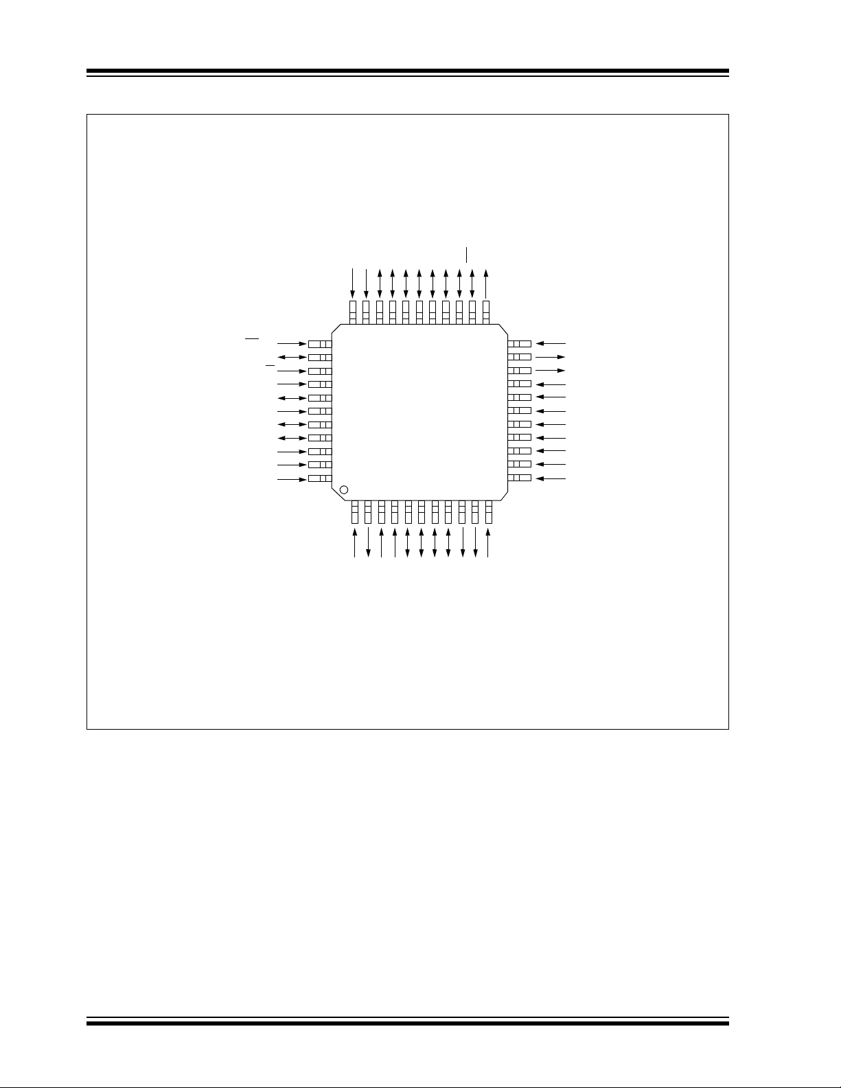
44-Pin TQFP and QFN
10 11234561
18
19
20
21
22
12
13
14
15
38
87
44
43
42
41
40
39
16
17
2930313233 232425262728
36
34
35
9
37
ENC424J600
VSSOSC
AD4
OSC2
OSC1
VDDOSC
AD5
AD6
LEDB
LEDA
TPOUT+
TPOUT-
VSSTX
AD9
AD10
AD11
AD12
SI/RD/RW
SCK/AL
VSS
AD7
RBIAS
VSSPLL
VDDPLL
VSSRX
VDDTX
VDDRX
TPINTPIN+
INT/SPISEL
CLKOUT
AD8
PSPCFG0
AD14
VSS
AD13
VCAP
AD0
SO/WR/EN
CS
/CS
AD1
AD2
V
DD
AD3
VSSTX
Pin Diagrams
DS39935C-page 2 2010 Microchip Technology Inc.
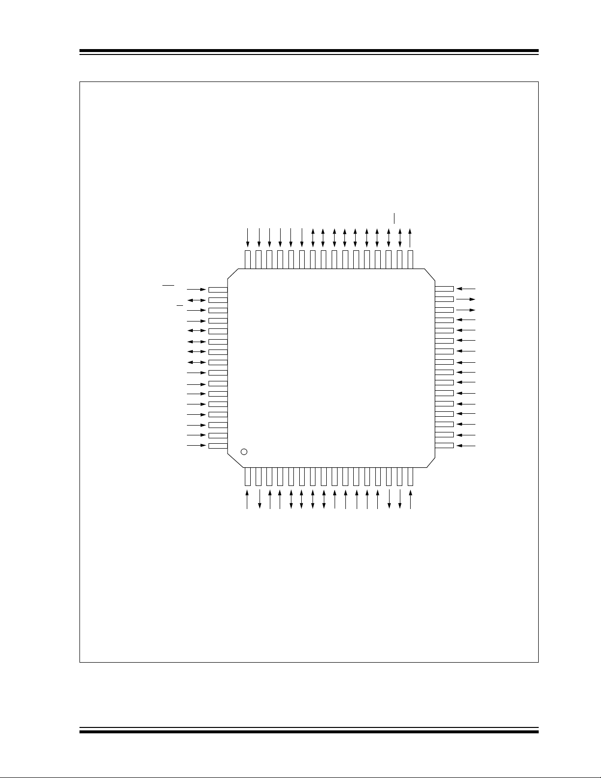
12345678910111213141516
48 47 46 45 44 43 42 41 40 39 38 37 36 35 34 33
64
63
62
61
60
59
58
57
56
55
54
53
52
51
50
49
17
18
19
20
21
22
23
24
25
26
27
28
29
30
31
32
ENC624J600
A12
PSPCFG2
A14/PSPCFG1
A13
A11
A10
A9
A8
A7
A5
A4
A3
A2
A1
WRH/B1SEL
A6
A0
PSPCFG3
AD7
AD6
AD5
AD4
OSC1
OSC2
VSSOSC
VDDOSC
CLKOUT
LEDB
LEDA
AD11
AD10
AD9
AD8
TPIN-
VSSTX
VDDTX
TPOUT-
TPOUT+
VSSTX
VSS
AD15
AD14
AD13
AD12
VSSRX
RBIAS
VDDPLL
VDDRX
VSSPLL
INT/SPISEL
CS/CS
SO/WR/WRL/EN/B0SEL
SI/RD/RW
SCK/AL/PSPCFG4
AD0
AD1
AD2
VDD
VCAP
VSS
AD3
VDD
VDD
TPIN+
64-Pin TQFP
ENC424J600/624J600
Pin Diagrams (Continued)
2010 Microchip Technology Inc. DS39935C-page 3

ENC424J600/624J600
Table of Contents
1.0 Device Overview .......................................................................................................................................................................... 5
2.0 External Connections ................................................................................................................................................................... 9
3.0 Memory Organization ................................................................................................................................................................. 17
4.0 Serial Peripheral Interface (SPI)................................................................................................................................................. 39
5.0 Parallel Slave Port Interface (PSP) ............................................................................................................................................ 51
6.0 Ethernet Overview...................................................................................................................................................................... 71
7.0 Reset .......................................................................................................................................................................................... 73
8.0 Initialization................................................................................................................................................................................. 75
9.0 Transmitting and Receiving Packets .......................................................................................................................................... 83
10.0 Receive Filters............................................................................................................................................................................ 95
11.0 Flow Control ............................................................................................................................................................................. 105
12.0 Speed/Duplex Configuration and Auto-Negotiation.................................................................................................................. 109
13.0 Interrupts .................................................................................................................................................................................. 117
14.0 Direct Memory Access (DMA) Controller ................................................................................................................................. 123
15.0 Cryptographic Security Engines ............................................................................................................................................... 125
16.0 Power-Saving Features............................................................................................................................................................ 137
17.0 Electrical Characteristics .......................................................................................................................................................... 141
18.0 Packaging Information.............................................................................................................................................................. 149
Appendix A: Revision History............................................................................................................................................................. 157
Index .................................................................................................................................................................................................. 159
The Microchip Web Site..................................................................................................................................................................... 163
Customer Change Notification Service .............................................................................................................................................. 163
Customer Support .............................................................................................................................................................................. 163
Reader Response .............................................................................................................................................................................. 164
Product Identification System............................................................................................................................................................. 165
TO OUR VALUED CUSTOMERS
It is our intention to provide our valued customers with the best documentation possible to ensure successful use of your Microchip
products. To this end, we will continue to improve our publications to better suit your needs. Our publications will be refined and
enhanced as new volumes and updates are introduced.
If you have any questions or comments regarding this publication, please contact the Marketing Communications Department via
E-mail at docerrors@microchip.com or fax the Reader Response Form in the back of this data sheet to (480) 792-4150. We
welcome your feedback.
Most Current Data Sheet
To obtain the most up-to-date version of this data sheet, please register at our Worldwide Web site at:
http://www.microchip.com
You can determine the version of a data sheet by examining its literature number found on the bottom outside corner of any page.
The last character of the literature number is the version number, (e.g., DS30000A is version A of document DS30000).
Errata
An errata sheet, describing minor operational differences from the data sheet and recommended workarounds, may exist for current
devices. As device/documentation issues become known to us, we will publish an errata sheet. The errata will specify the revision
of silicon and revision of document to which it applies.
To determine if an errata sheet exists for a particular device, please check with one of the following:
• Microchip’s Worldwide Web site; http://www.microchip.com
• Your local Microchip sales office (see last page)
When contacting a sales office, please specify which device, revision of silicon and data sheet (include literature number) you are
using.
Customer Notification System
Register on our web site at www.microchip.com to receive the most current information on all of our products.
DS39935C-page 4 2010 Microchip Technology Inc.

ENC424J600/624J600
1.0 DEVICE OVERVIEW
This document contains device-specific information for
the following devices:
• ENC424J600
• ENC624J600
The ENC424J600 and ENC624J600 are stand-alone,
Fast Ethernet controllers with an industry standard
Serial Peripheral Interface (SPI) or a flexible parallel
interface. They are designed to serve as an Ethernet
network interface for any microcontroller equipped with
SPI or a standard parallel port.
ENC424J600/624J600 devices meet all of the
IEEE 802.3 specifications applicable to 10Base-T and
100Base-TX Ethernet, including many optional
clauses, such as auto-negotiation. They incorporate a
number of packet filtering schemes to limit incoming
packets. They also provide an internal, 16-bit wide
DMA for fast data throughput and support for hardware
IP checksum calculations.
For applications that require the security and authentication features of SSL, TLS and other protocols related
to cryptography, a block of security engines is provided.
The engines perform RSA, Diffie-Hellman, AES, MD5
and SHA-1 algorithm computations, allowing reduced
code size, faster connection establishment and
throughput, and reduced firmware development effort.
Communication with the microcontroller is
implemented via the SPI or parallel interface, with data
rates ranging from 14 Mbit/s (SPI) to 160 Mbit/s
(demultiplexed, 16-bit parallel interface). Dedicated
pins are used for LED link and activity indication and for
transmit/receive/DMA interrupts.
A generous 24-Kbyte on-chip RAM buffer is available
for TX and RX operations. It may also be used by the
host microcontroller for general purpose storage.
Communication protocols, such as TCP, can use this
memory for saving data which may need to be
retransmitted.
For easy end product manufacturability, each
ENC624J600 family device is preprogrammed with a
unique nonvolatile MAC address. In most cases, this
allows the end device to avoid a serialized
programming step.
The only functional difference between the
ENC424J600 (44-pin) and ENC624J600 (64-pin)
devices are the number of parallel interface options
they support. These differences, along with a summary
of their common features, are provided in Table 1-1. A
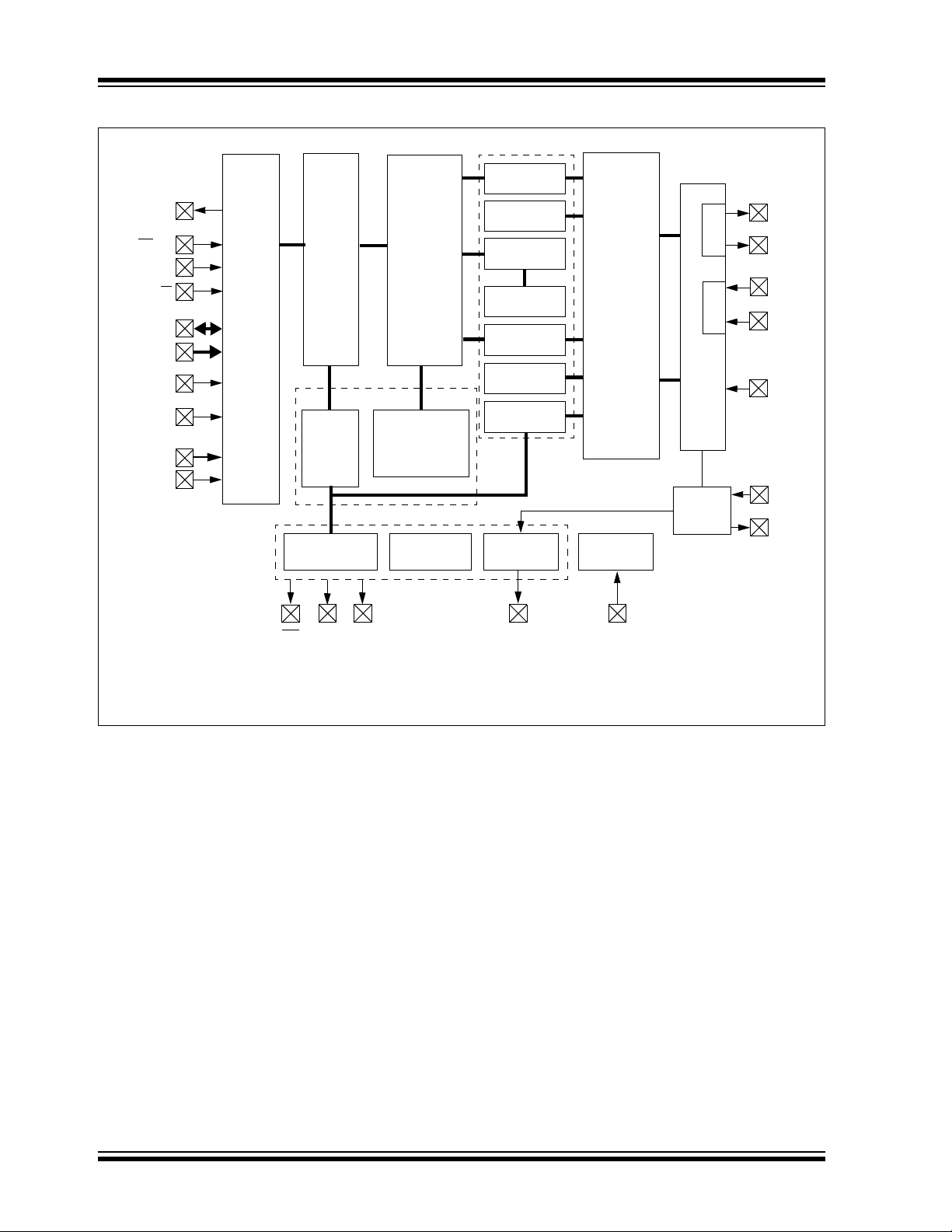
general block diagram for the devices is shown in
Figure 1-1.
A list of the pin features, sorted by function, is
presented in Table 1-2.
TABLE 1-1: DEVICE FEATURES FOR ENC424J600/624J600
Feature ENC424J600 ENC624J600
Pin Count 44 64
Ethernet Operating Speed 10/100 Mbps (auto-negotiate, auto-sense or manual)
Ethernet Duplex Modes Half and Full (auto-negotiate and manual)
Ethernet Flow Control Pause and Backpressure (auto and manual)
Buffer Memory (bytes) 24K (organized as 12K word x 16)
Internal Interrupt Sources 11 (mappable to a single external interrupt flag)
Serial Host Interface (SPI) Yes Yes
Parallel Host Interface:
Operating modes 2 8
Muliplexed, 8-bit Yes Yes
16-bit No Yes
Demultiplexed, 8-bit No Yes
16-bit No Yes
Cryptographic Security Options:
AES, 128/192/256-bit Yes Yes
MD5/SHA-1 Yes Yes
Modular Exponentiation, 1024-bit Yes Yes
Receive Filter Options Accept or reject packets with CRC match/mismatch, runt error collect
or reject, Unicast, Not-Me Unicast, Multicast, Broadcast,
Magic Packet™, Pattern Table and Hash Table
Packages 44-Pin TQFP, QFN 64-Pin TQFP
2010 Microchip Technology Inc. DS39935C-page 5
ENC424J600/624J600
24 Kbytes
DMA and
Checksum
TX Control
RX Control
Arbiter
Flow Control
Host Interface
Control
Registers
25 MHz
Power-on
PHY
MII
Interface
MIIM
Interface
TPOUT+
TPOUT-
TPIN+
TPIN-
TX
RX
RBIAS
OSC1
OSC2
Control Logic
CS/CS
SI/RD/RW
SO
SCK/AL
INT
VCAP
CLKOUT
LEDA
LEDB
RX Filter
MAC
m3
m1
SRAM
Note 1: A<14:0>, AD15, WRL/B0SEL, WRH/B1SEL and PSPCFG<4:1> are available on 64-pin devices only. PSPCFG0 is available on 44-pin
devices only.
Reset
Oscillator
I/O
Interface
AD<15:0>
(1)
A<14:0>
(1)
Logic
Logic
Crypto Cores
Memory
Bus
Interface
SPIParallel Common
SPISEL
PSPCFGx
(1)
EN/B0SEL
(1)
WR/WRL/
WRH/
B1SEL
(1)
m0
m2
PLL
Vol ta ge
Regulator
FIGURE 1-1: ENC424J600/624J600 BLOCK DIAGRAM
DS39935C-page 6 2010 Microchip Technology Inc.

ENC424J600/624J600
TABLE 1-2: ENC424J600/624J600 PINOUT DESCRIPTIONS
Pin Name
AD0 38 53 I/O CMOS PSP Multiplexed Address Input and/or Bidirectional
AD1 39 54 I/O CMOS
AD2 40 55 I/O CMOS
AD3 41 56 I/O CMOS
AD4 5 5 I/O CMOS
AD5 6 6 I/O CMOS
AD6 7 7 I/O CMOS
AD7 8 8 I/O CMOS
AD8 25 35 I/O CMOS
AD9 26 36 I/O CMOS
AD10 27 37 I/O CMOS
AD11 28 38 I/O CMOS
AD12 29 39 I/O CMOS
AD13 30 40 I/O CMOS
AD14 31 41 I/O CMOS
AD15 — 42 I/O CMOS
A0 — 57 I CMOS PSP Demultiplexed Address Input Bus
A1 — 58 I CMOS
A2 — 59 I CMOS
A3 — 60 I CMOS
A4 — 61 I CMOS
A5 — 9 I CMOS
A6 — 10 I CMOS
A7 — 11 I CMOS
A8 — 12 I CMOS
A9 — 13 I CMOS
A10 — 19 I CMOS
A11 — 20 I CMOS
A12 — 43 I CMOS
A13 — 44 I CMOS
A14 — 45 I CMOS
AL 37 52 I CMOS PSP Address Latch
B0SEL — 50 I CMOS PSP Byte 0 Select
B1SEL — 48 I CMOS PSP Byte 1 Select
CLKOUT 23 33 O — Programmable Clock Output for External Use
CS
CS 34 49 I CMOS PSP Chip Select (active-high)
EN 35 50 I CMOS PSP R/W
INT 24 34 O — Interrupt Output (active-low)
LEDA 10 15 O — Programmable Ethernet Status/Activity LED
LEDB 9 14 O — Programmable Ethernet Status/Activity LED
Legend: I = Input; O = Output; P = Power; CMOS = CMOS compatible input buffer; ANA = Analog level input/output
Pin Number
Pin Type
44-Pin 64-Pin
34 49 I
Input
Buffer
CMOS
Description
Data Bus
SPI Chip Select (active-low)
Enable strobe
2010 Microchip Technology Inc. DS39935C-page 7

ENC424J600/624J600
TABLE 1-2: ENC424J600/624J600 PINOUT DESCRIPTIONS (CONTINUED)
Pin Name
OSC1 3 3 I ANA 25 MHz Crystal Oscillator/Clock Input
OSC2 2 2 O — 25 MHz Crystal Oscillator Output
PSPCFG0 32 — I CMOS PSP Mode Select 0
PSPCFG1 — 45 I CMOS PSP Mode Select 1
PSPCFG2 — 17 I CMOS PSP Mode Select 2
PSPCFG3 — 18 I CMOS PSP Mode Select 3
PSPCFG4 — 52 I CMOS PSP Mode Select 4
RBIAS 11 16 I ANA PHY Bias (external resistor) Connection
RD 36 51 I CMOS PSP Read Strobe
RW
SCK 37 52 I CMOS SPI Serial Clock Input
SI 36 51 I CMOS SPI Serial Data Input (from Master)
SO 35 50 O — SPI Serial Data Out (to Master)
SPISEL 24 34 I CMOS SPI/PSP Interface Select
TPIN- 17 27 I ANA Differential Ethernet Receive Minus Signal Input
TPIN+ 16 26 I ANA Differential Ethernet Receive Plus Signal Input
TPOUT- 21 31 O — Differential Ethernet Transmit Minus Signal Output
TPOUT+ 20 30 O — Differential Ethernet Transmit Plus Signal Output
CAP 43 63 P — Regulator External Capacitor connection
V
VDD 44 21, 47,
VDDOSC 4 4 P — Positive 3.3V Power Supply for 25 MHz Oscillator
VDDPLL 12 22 P — Positive 3.3V Power Supply for PHY PLL Circuitry
VDDRX 15 25 P — Positive 3.3V Power Supply for PHY RX Circuitry
VDDTX 18 28 P — Positive 3.3V Power Supply for PHY TX Circuitry
VSS 33, 42 46, 62 P — Ground Reference for Digital Logic
VSSOSC 1 1 P — Ground Reference for 25 MHz Oscillator
VSSPLL 13 23 P — Ground Reference for PHY PLL Circuitry
VSSRX 14 24 P — Ground Reference for PHY RX Circuitry
VSSTX 19, 22 29, 32 P — Ground Reference for PHY TX Circuitry
WR 35 50 I CMOS PSP Write Strobe
WRH — 48 I CMOS PSP Write High Strobe
WRL — 50 I CMOS PSP Write Low Strobe
Legend: I = Input; O = Output; P = Power; CMOS = CMOS compatible input buffer; ANA = Analog level input/output
Pin Number
Pin Type
44-Pin 64-Pin
36 51 I CMOS PSP Combined Read/Write Signal
P — Positive 3.3V Power Supply for Digital Logic
64
Input
Buffer
Description
DS39935C-page 8 2010 Microchip Technology Inc.
ENC424J600/624J600
C1
(3)
C2
(3)
XTAL
OSC2
RS
(1)
OSC1
RF
(2)
To Internal Logic
Note 1: A series resistor, RS, may be required for
crystals with a low drive strength specification
or when using large loading capacitors.
2: The feedback resistor, RF , is typically 1.5 M
approx.
3: The load capacitors’ value should be derived
from the capacitive loading specification
provided by the crystal manufacture.
ENCX24J600
3.3V Clock from
External System
(1)
OSC1
OSC2
Open
Note 1: Duty cycle restrictions must be observed.
ENCX24J600
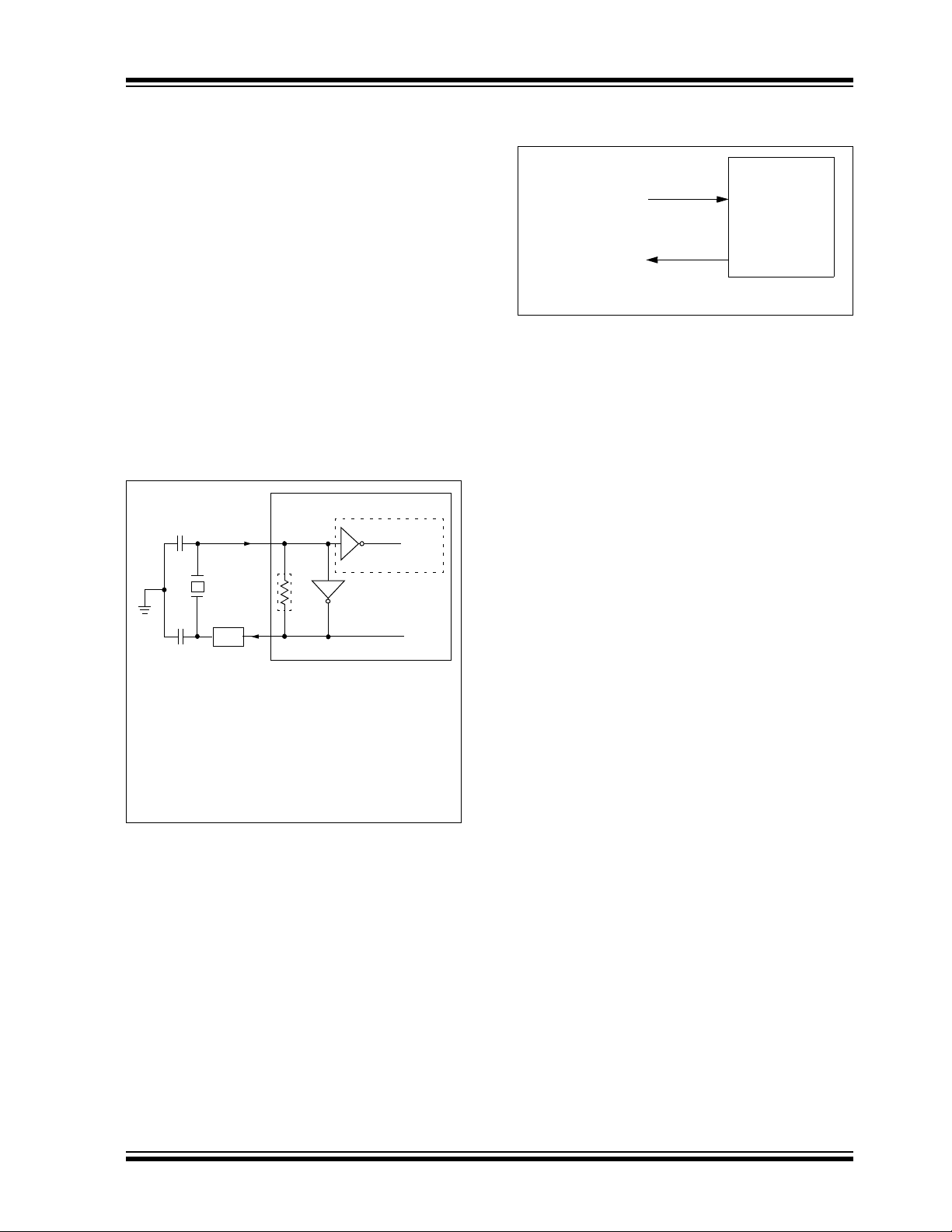
2.0 EXTERNAL CONNECTIONS
2.1 Oscillator
ENC424J600/624J600 devices are designed to
operate from a fixed 25 MHz clock input. This clock can
be generated by an external CMOS clock oscillator or
a parallel resonant, fundamental mode 25 MHz crystal
attached to the OSC1 and OSC2 pins. Use of a crystal,
rated for series resonant operation, will oscillate at an
incorrect frequency. To comply with IEEE 802.3 Ethernet
timing requirements, the clock must have no more than
±50 ppm of total error; avoid using resonators or clock
generators that exceed this margin.
When clocking the device using a crystal, follow the
connections shown in Figure 2-1. When using a CMOS
clock oscillator or other external clock source, follow
Figure 2-2.
FIGURE 2-1: CRYSTAL OSCILLATOR
OPERATION
FIGURE 2-2: EXTERNAL CLOCK
SOURCE
2.2 CLKOUT Pin
The Clock Out pin (CLKOUT) is provided for use as the
host controller clock or as a clock source for other
devices in the system. Its use is optional.
The 25 MHz clock applied to OSC1 is multiplied by a
PLL to internally generate a 100 MHz base clock. This
100 MHz clock is driven through a configurable
postscaler to yield a wide range of different CLKOUT
frequencies. The PLL multiplication adds clock jitter,
subject to the PLL jitter specification in Section 17.0
“Electrical Characteristics”. However, the postscaler
ensures that the clock will have a nearly ideal duty
cycle.
The CLKOUT function is enabled and the postscaler is
selected via the COCON<3:0> bits (ECON2<11:8>).
To create a clean clock signal, the CLKOUT output and
COCON bits are unaffected by all resets and
power-down modes. The CLKOUT function is enabled
out of POR and defaults to producing a 4 MHz clock.
This allows the device to directly clock the host
processor.
When the COCON bits are written with a new
configuration, the CLKOUT output transitions to the
new frequency without producing any glitches. No high
or low pulses with a shorter period than the original or
new clock are generated.
2010 Microchip Technology Inc. DS39935C-page 9

ENC424J600/624J600
VDD
VCAP
VSS
ENCX24J600
10 F
3.3V
0.1 F
Regulator
+3.3V
I/O, PHY
+1.8V
Core, RAM,
MAC
RBIAS
ENCX24J600
12.4k
1%
PHY
2.3 Voltage and Bias Pin
2.3.1 VDD AND VSS PINS
To reduce on-die noise levels and provide for the
high-current demands of Ethernet, there are many
power pins on ENC424J600/624J600 devices:
•VDD and VSS
•VDDOSC and VSSOSC
•VDDPLL and VSSPLL
•VDDRX and VSSRX
•VDDTX and VSSTX
Each VDD and VSS pin pair above should have a 0.1 F
ceramic bypass capacitor placed as close to the pins as
possible. For best EMI emission suppression, other
smaller capacitors, such as 0.001 F, should be placed
immediately across V
All VDD power supply pins must be externally connected to the same 3.3V ±10% power source. Similarly,
all VSS supply references must be externally connected
to the same ground node. If a ground connection
appears on two pins (e.g., V
do not allow either to float. In addition, it is
recommended that the exposed bottom metal pad on
the 44-pin QFN package be tied to VSS.
Placing ferrite beads or inductors between any two of
the supply pins (e.g., between VDDOSC and VDDRX) is
not recommended. However, it is acceptable to isolate
DD
all of the V
supplies from the main circuit power supply through a single ferrite bead or inductor, if desired
for supply noise suppression reasons. Such isolation is
generally not necessary.
DDTX/VSSTX and VDDPLL/VSSPLL.
SSTX), connect both pins;
FIGURE 2-3: VCAP CONNECTIONS
2.3.3 RBIAS PIN
The internal analog circuitry in the PHY module
requires that an external 12.4 kΩ, 1% resistor be
attached from RBIAS to ground, as shown in
Figure 2-4. The resistor influences the TPOUT+/signal amplitude. The RBIAS resistor should be placed
as close as possible to the chip with no immediately
adjacent signal traces in order to prevent noise
capacitively coupling into the pin and affecting the
transmit behavior. It is recommended that the resistor
be a surface mount type.
FIGURE 2-4: RBIAS RESISTOR
2.3.2 VCAP PIN
Most of the device’s digital logic operates at a nominal
1.8V. This voltage is supplied by an on-chip voltage
regulator, which generates the digital supply voltage
from the VDD rail. The only external component
required is an external filter capacitor, connected from
the VCAP pin to ground, as shown in Figure 2-3. A value
of at least 10 F is recommended.
The capacitor must also have a relatively low Equivalent Series Resistance (ESR). It is recommended that
a low-ESR capacitor (ceramic, tantalum or similar)
should be used and high-ESR capacitors (such as
aluminum electrolytic) should be avoided.
The internal regulator is not designed to drive external
loads; therefore, do not attach other circuitry to V
DS39935C-page 10 2010 Microchip Technology Inc.
CAP.
ENC424J600/624J600
ENCX24J600
TPOUT+
TPOUT-
TPIN+
TPIN-
3.3V
1
2
3
4
5
6
7
8
RJ-45
1:1 CT
1:1 CT
1000 pF, 2 kV
75757575
49.9, 1%
49.9
, 1%
49.9, 1%
49.9, 1%
0.01 F
0.01
F
1
6.8 n
F, 1 0 %
6.8 n
F, 1 0 %
10, 1/12W, 1%
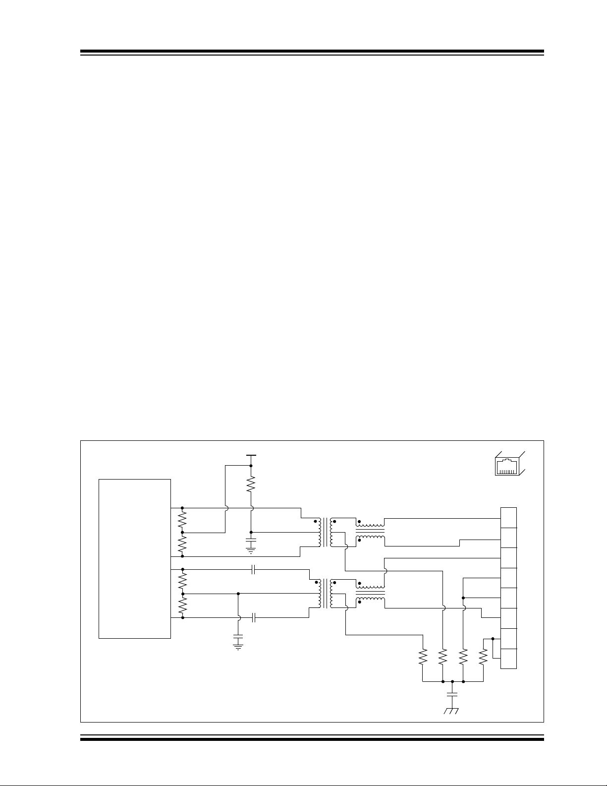
2.4 Ethernet Signal Pins and External Magnetics
Typical applications for ENC424J600/624J600 devices
require an Ethernet transformer module, and a few
resistors and capacitors to implement a complete
IEEE 802.3 compliant 10/100 Ethernet interface, as
shown in Figure 2-5.
The Ethernet transmit interface consists of two pins:
TPOUT+ and TPOUT-. These pins implement a
differential pair and a current-mode transmitter. To
generate an Ethernet waveform, ordinary applications
require the use of a 1:1 center tapped pulse
transformer, rated for 10/100 or 10/100/1000 Ethernet
operations. When the Ethernet module is enabled and
linked with a partner, current is continually sunk
through both TPOUT pins. When the PHY is actively
transmitting, a differential voltage is created on the
Ethernet cable by varying the relative current sunk by
TPOUT+ compared to TPOUT-.
The Ethernet receive interface similarly consists of a
differential pair: TPIN+ and TPIN-. To meet IEEE 802.3
compliance and help protect against electrostatic discharge, these pins are normally isolated from the
Ethernet cable by a 1:1 center tapped transformer
(available in the same package as the TX transformer).
Internally, the PHY uses a high-speed ADC to sample
the receive waveform and decodes it using a DSP. The
PHY implements many robustness features, including
baseline wander correction (applicable to 100Base-TX)
and automatic RX polarity correction (applicable to
10Base-T).
Four 49.9Ω, 1% resistors are required for proper
termination of the TX and RX transmission lines. If the
board layout necessitates long traces between the
ENCX24J600 and Ethernet transformers, the termination resistors should be placed next to the silicon
instead of the transformers.
On the receive signal path, two 6.8 nF 10% capacitors
are used. These capacitors, in combination with the
49.9 termination resistors, form an RC high-pass filter
to reduce baseline wander. For best performance,
these capacitors should not be omitted or changed.
The various remaining capacitors provide DC current
blocking and provide stability to the common-mode
voltage of both of the differential pairs. The TPIN+/pins weakly output a common-mode voltage that is
acceptable to the internal ADC. For proper operation,
do not attempt to externally force the TPIN+/common-mode voltage to some other value.
The 10Ω 1% resistor provides a current path from the
power supply to the center tap of the TX transformer.
As mentioned previously, the TPOUT+/- pins
implement a Current mode drive topology in which the
pins are only capable of sinking current; they do not
produce a direct voltage. This current path through the
transformer generates the transmit waveform. The 10Ω
resistor reduces the amount of heat that the PHY would
have to dissipate, and therefore, must have a power
rating of 1/12W or better.
FIGURE 2-5: TYPICAL ETHERNET MAGNETICS CONNECTIONS
2010 Microchip Technology Inc. DS39935C-page 11
ENC424J600/624J600
1:1 CT
PHY
RJ-45
180
LEDA
or
LEDB
LED
180
LEDA
LEDB
LED
Bi-Color
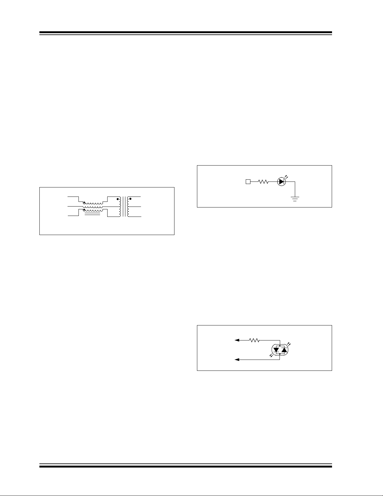
2.4.1 ADDITIONAL EMI AND LAYOUT CONSIDERATIONS
To reduce EMI emissions, common-mode chokes are
shown adjacent to the transformers on the cable
(RJ-45) side. These chokes come standard in typical
Ethernet transformer modules. Because the
ENCX24J600 PHY uses a current-mode drive topology, the transmit choke must normally be located on
the cable side of the transmit transformer. Orienting the
magnetics such that the choke is on the PHY side of the
transmit transformer usually results in a distorted,
non-compliant transmit waveform. However, some
magnetics which wrap the TX center tap wire around
the TX choke core can also be used to generate a
compliant waveform (Figure 2-6). These types of transformers may be desirable in some Power-over Ethernet
(PoE) applications.
By default on POR, LEDA displays the Ethernet link
status, while LEDB displays PHY-level TX/RX activity.
Because the LEDs operate at the PHY level, RX
activity will be displayed on LEDB any time Ethernet
packets are detected, regardless of if the packet is valid
and meets the correct RX filtering criteria.
Normally, the device illuminates the LED by sourcing
current out of the pin, as shown in Figure 2-7. Connecting the LED in reverse, with the anode connected to
DD
and the cathode to LEDA/LEDB (through a
V
current-limiting resistor), causes the LED to show
“inverted sense” behavior, lighting the LED when it
should be off and extinguishing the LED when the LED
should be on.
FIGURE 2-7: SINGLE COLOR LED
CONNECTION
FIGURE 2-6: ALTERNATE TX CHOKE
TOP OL O G Y
Both LEDs automatically begin operation whenever
power is applied, a 25 MHz clock is present and the
Ethernet magnetics are present and wired correctly. A
connection to the host microcontroller via the SPI or
The common-mode choke on the RX interface can be
placed on either the cable side or PHY side of the
receive transformer. Recommended and required magnetics characteristics are located in Section 17.0
“Electrical Characteristics”.
The four 75Ω resistors and high-voltage capacitor in
Figure 2-5 are intended to prevent each of the twisted
pairs in the Ethernet cables from floating and radiating
EMI. Their implementation may require adjustment in
PoE applications.
Unless the TX and RX signal pairs are kept short, they
should be routed between the ENCX24J600 and the
Ethernet connector following differential routing rules.
Like Ethernet cables, 100Ω characteristic impedance
should be targeted for the differential traces. The use of
vias, which introduce impedance discontinuities,
should be minimized. Other board level signals should
not run immediately parallel to the TX and RX pairs to
minimize capacitive coupling and crosstalk.
2.5 LEDA and LEDB Pins
The LEDA and LEDB pins provide dedicated LED
status indicator outputs. The LEDs are intended to
display link status and TX/RX activity among other
programmable options; however, the use of one or both
is entirely optional. The pins are driven automatically by
the hardware and require no support from the host
microcontroller. Aside from the LEDs themselves, a
current-limiting resistor is generally the only required
component.
DS39935C-page 12 2010 Microchip Technology Inc.
PSP interface is not required. LEDA and LEDB can,
therefore, be used as a quick indicator of successful
assembly during initial prototype development.
2.5.1 USING BI-COLOR LEDs
In space constrained applications, it is frequently desir-
able to use a single bi-color LED to display multiple
operating parameters. These LEDs are connected
between LEDA and LEDB, as shown in Figure 2-8.
FIGURE 2-8: BI-COLOR LED
CONNECTION
ENCX24J600 devices include two special hardware
display modes to make maximal use of a bi-color LED.
These modes are selected when the LACFG<3:0> and
LBCFG<3:0> bits (EIDLED<15:8>) are set to ‘1111’ or
‘1110’. In these configurations, the link state turns the
LED on, the speed/duplex state sets the LED color and
TX/RX events cause the LED to blink off. If a link is
present, no TX/RX events are occurring and the
speed/duplex state is 100 Mbps/full duplex,
respectively, then the LEDB pin will be driven high while
LEDA will be driven low.
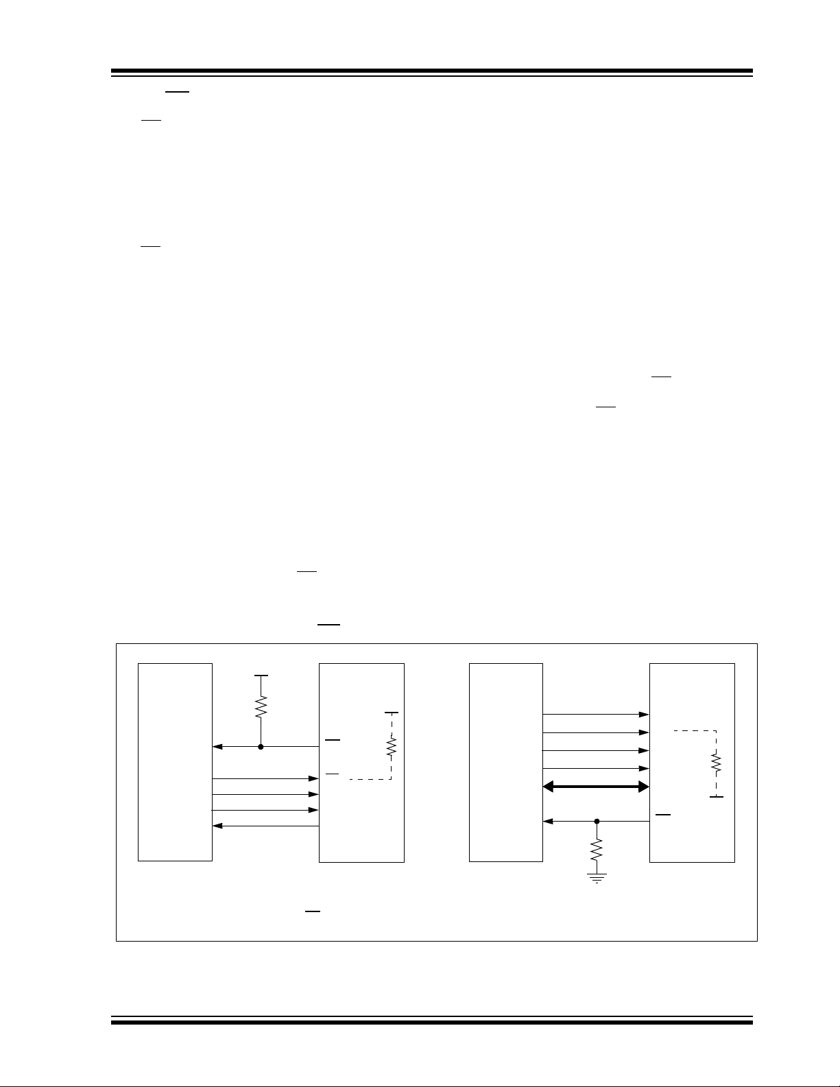
ENC424J600/624J600
I/O
SCK
SDO
SDI
INT0
MCU
CS
SCK
SI
SO
INT
/SPISEL
ENCX24J600
3.3V
100k
PMALL
PMCS2
RMRD
PMWR
INT0
MCU
AL
CS
RD
WR
INT
/SPISEL
ENCX24J600
ADx
PMAx/PMDx
100k
SPI Selected PSP Selected (Mode 5 shown)
~2.2V
VSS
(internal weak pull-up on CS
enabled) (internal weak pull-down on CS enabled)
2.6 I
The INT
NT Pin
pin is an active-low signal that is used to flag
interrupt events to external devices. Depending on the
application, it can be used to signal the host microcontroller whenever a packet has been received or
transmitted, or that some other asynchronous
operation has occurred. It can also be used to wake-up
the microcontroller or other system components based
on LAN activity; its use is optional.
The INT pin is driven high when no interrupt is pending
and is driven low when an interrupt has occurred. It
does not go into a high-impedance state, except during
initial power-on while the multiplexed SPISEL pin
function is being used.
Since ENC424J600/624J600 devices incorporate a
buffer for storing transmit and receive packets, the host
microcontroller never needs to perform real-time
operations on the device. The microcontroller can poll
the device registers to discover if the device status has
changed.
2.7 Host Interface Pins
For the maximum degree of flexibility in interfacing with
microcontrollers, ENC424J600/624J600 devices offer
a choice between a serial interface based on the Serial
Peripheral Interface (SPI) standard, and a flexible 8 or
16-bit parallel slave port (PSP) interface. Only one
interface may be used at any given time.
The I/O interface is hardware selected on power-up
using the SPISEL function on the INT/SPISEL pin. This
is done by latching in the voltage level applied to the pin
approximately 1 to 10 s after power is applied to the
device and the device exits Power-on Reset. If SPISEL
is latched at a logic high state, the serial interface is
enabled. If SPISEL is latched at a logic low state, the
PSP interface is enabled. Figure 2-9 shows example
connections required to select the SPI or PSP interface
upon power-up.
To ensure the SPI interface is selected upon power-up,
an external pull-up resistor to VDD must be connected
to the SPISEL pin. Alternatively, if the parallel interface
is to be used, a pull-down resistor to V
SS must be
connected to the SPISEL pin. In most circuits, it is recommended that a 100 kΩ or smaller resistor be used to
ensure that the correct logic level is latched in reliably.
If a large capacitance is present in the SPISEL circuit,
such as from stray capacitance, a smaller pull-up or
pull-down resistor may be required to compensate and
ensure the correct level is sensed during power-up.
As SPISEL is multiplexed with the INT
interrupt output
function, a direct connection to VDD or VSS without a
resistor is prohibited. If INT
is connected to the host
microcontroller, the microcontroller must leave this
signal in a high-impedance state and not attempt to
drive it to an incorrect logic state during power-up.
DD supply has a slow ramp rate, the device will
If the V
exit POR, exceed the 1 to 10 s latch timer and sample
the SPISEL pin state before VDD has reached the specified minimum operating voltage of the device. In this
case, the device will still latch in the correct value,
assuming the minimum VIH (D004) or maximum VIL
(D006) specification is met, which is a function of VDD.
FIGURE 2-9: USING THE INT
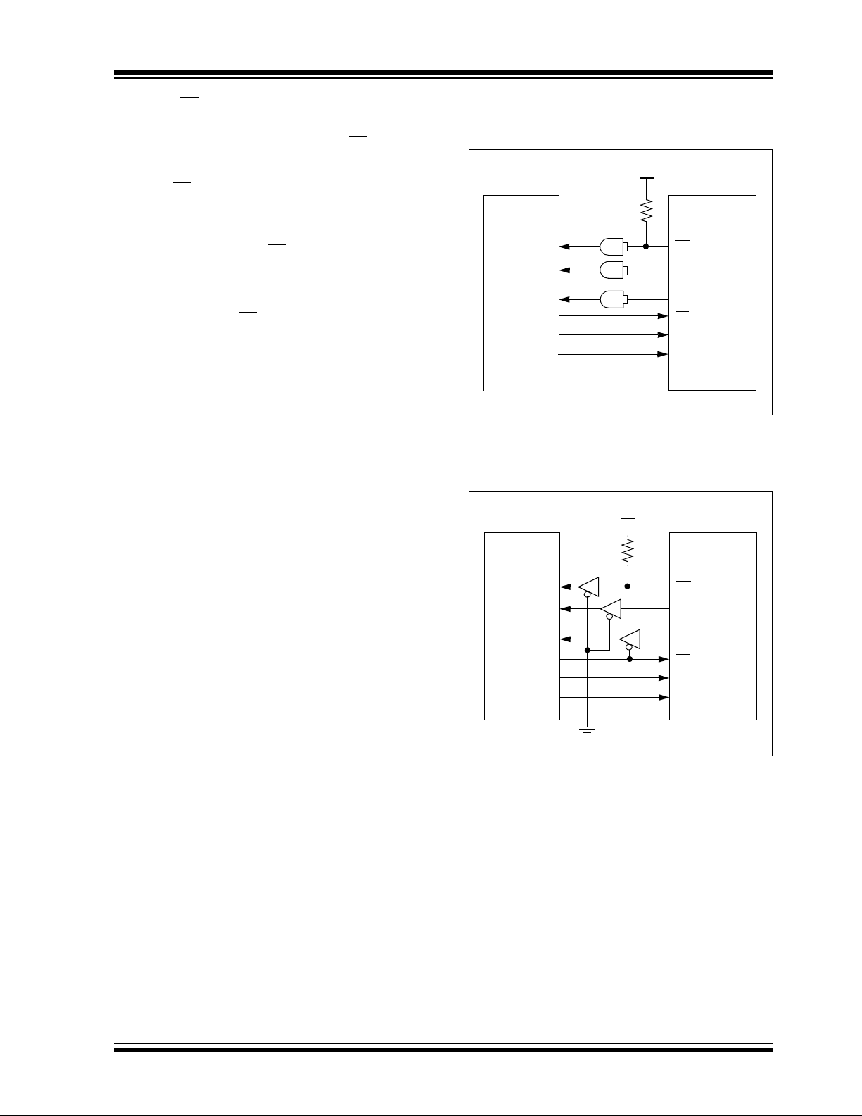
/SPISEL PIN TO SELECT THE I/O INTERFACE
2010 Microchip Technology Inc. DS39935C-page 13
ENC424J600/624J600
2.7.1 SPI
When enabled, the SPI interface is implemented with
four pins:
•CS
•SO
•SI
•SCK
All four of these pins must be connected to use the SPI
interface.
, SI and SCK input pins are 5V tolerant. The SO
The CS
pin is also 5V tolerant when in a high-impedance state.
SO is always high-impedance when CS
logic high (i.e., chip not selected).
When the SPI interface is enabled, all PSP interface
pins (except PSPCFG2 and PSPCFG3 on
ENC624J600 devices) are unused. They are placed in
a high-impedance state and their input buffers are disabled. For best ESD performance, it is recommended
that the unused PSP pins be tied to either V
However, these pins may be left floating if it is desirable
for board level layout and routing reasons.
When using an ENC624J600 device in SPI mode, it is
recommended that the PSPCFG2 and PSPCFG3 pins
SS
be tied to either V
be left floating. The particular state used is unimportant.
or any logic high voltage, and not
is connected to
SS or VDD.
2.7.2 PSP
Depending on the particular device, the PSP interface
is implemented with up to 34 pins. The interface is
highly configurable to accommodate many different
parallel interfaces; not all available pins are used in
every configuration. Up to 8 different operating modes
are available. These are explained in detail in
Section 5.0 “Parallel Slave Port Interface (PSP)”.
The PSPCFG pins control which parallel interface
mode is used. The values on these pins are latched
upon device power-up in the same manner as the
SPISEL pin. The combinations of V
ages on the different PSPCFG mode pins determine
the PSP mode according to Table 2-1.
On ENC424J600 devices, only PSP Modes 5 and 6
(8-bit width, multiplexed data and address) are
available. The mode is selected by applying V
VDD, respectively, to PSPCFG0.
On ENC624J600 devices, all eight PSP modes are
available and are selected by connecting the
PSPCFG<4:1> pins directly to V
mode selection is encoded such that the multiplexed
pin functions, AD14 (on PSPCFG1) and SCK/AL (on
PSPCFG4), are used only in the “don’t care” positions.
Therefore, pull-up/pull-down resistors are not required
for these pins.
All PSP pins, except for AD<15:0>, are inputs to the
ENC624J600 family device and are 5V tolerant. The
AD<15:0> pins are bidirectional I/Os and are 5V
tolerant in Input mode. The pins are always inputs
when the CS signal is low (chip not selected).
Any unused PSP pins are placed in a high-impedance
state. However, it is recommended that they be tied to
either Vss or a logic high voltage and not be left floating.
DD and VSS volt-
SS or
DD or ground. The
TABLE 2-1: PSP MODE SELECTION FOR ENC424J600/624J600 DEVICES
Interface
Mode
PSP Mode 5 Pull Down 0 ———— AL, CS, RD, WR, AD<14:0>
PSP Mode 6 Pull Down 1 ———— AL, CS, RW, EN, AD<14:0>
PSP Mode 1 Pull Down —x000 CS, RD, WR, A14:A0, AD<7:0>
PSP Mode 2 Pull Down —x001 CS, RW
PSP Mode 3 Pull Down —x100 CS, RD, WRL, WRH, A<13:0>, AD<15:0>
PSP Mode 4 Pull Down —x101 CS, RW, B0SEL, B1SEL, A<13:0>, AD<15:0>
PSP Mode 5 Pull Down —001x AL, CS, RD, WR, AD<14:0>
PSP Mode 6 Pull Down —101x AL, CS, RW
PSP Mode 9 Pull Down —011x AL, CS, RD, WRL, WRH, AD<15:0>
PSP Mode 10 Pull Down —111x AL, CS, RW
Legend: x = don’t care, 0 = logic low (tied to VSS), 1 = logic high (tied to VDD), — = pin not present
INT
/SPISEL
01234
PSPCFG
Pins Used
44-Pin
64-Pin
, EN, A14:A0, AD<7:0>
, EN, AD<14:0>
, B0SEL, B1SEL, AD<15:0>
DS39935C-page 14 2010 Microchip Technology Inc.
ENC424J600/624J600
I/O
SCK
SDO
SDI
INTx
MCU
CS
SCK
SI
SO
INT
/SPISEL
ENCX24J600
CLKOUT
OSC1
3.3V
100k
I/O
SCK
SDO
SDI
INTx
MCU
CS
SCK
SI
SO
INT
/SPISEL
ENCX24J600
CLKOUT
OSC1
3.3V
100k
2.7.3 CS
/CS PIN
The chip select functions for the serial and parallel
interfaces are shared on one common pin, CS
/CS. This
pin is equipped with both internal weak pull-up and
weak pull-down resistors. If the SPI interface is
selected (CS
), the pull-up resistor is automatically
enabled and the pull-down resistor is disabled. If the
PSP interface is chosen (CS), the pull-down resistor is
automatically enabled and the pull-up resistor is
disabled. This allows the CS
/CS pin to stay in the
unselected state when not being driven, avoiding the
need for an external board level resistor on this pin.
When enabled by using SPI mode, the internal weak
pull-up only pulls the CS
/CS pin up to approximately
VDD-1.1V or around 2.2V at typical conditions without
any loading; it does not pull all the way to VDD. When
using the PSP interface, the pull-down will be enabled,
which is capable of pulling all the way to VSS when
unloaded.
2.8 Digital I/O Levels
All digital output pins on ENC424J600/624J600
devices contain CMOS output drivers that are capable
of sinking and sourcing up to 18 mA continuously. All
digital inputs and I/O pins operating as inputs are 5V
tolerant. These features generally mean that the
ENCX24J600 can connect directly to the host
microcontroller without the need of any glue logic.
However, some consideration may be necessary when
interfacing with 5V systems.
Since the digital outputs drive only up to the V
voltage (3.3V nominally), the voltage may not be high
enough to ensure a logical high is detected by 5V
systems which have high input thresholds. In such
cases, unidirectional level translation from the 3.3V
ENCX24J600 up to the 5V host microcontroller may be
needed.
When using the SPI interface, an economical 74HCT08
(quad AND gate), 74ACT125 (quad 3-state buffer) or
other 5V CMOS chip with TTL level input buffers may
be used to provide the necessary level shifting. The
use of 3-state buffers permits easy integration into
systems which share the SPI bus with other devices.
However, users must make certain that the propagation delay of the level translator does not reduce the
maximum SPI frequency below desired levels.
Figure 2-10 and Figure 2-11 show two example
translation schemes.
When using the PSP interface, eight, or all sixteen of
the ADx pins, may need level translation when performing read operations on the ENCX24J600. The 8-bit
74ACT245 or 16-bit 74ACT16245 bus transceiver, or
similar devices, may be useful in these situations.
DD
FIGURE 2-10: LEVEL SHIFTING ON THE
SPI INTERFACE USING
AND GATES
FIGURE 2-11: LEVEL SHIFTING ON THE
SPI INTERFACE USING
3-STATE BUFFERS
2010 Microchip Technology Inc. DS39935C-page 15

ENC424J600/624J600
NOTES:
DS39935C-page 16 2010 Microchip Technology Inc.

ENC424J600/624J600
0000h
5FFFh
00h
SRAM Buffer
Unimplemented
7800h
7C4Fh
Bank 0
Bank 1
Bank 2
Bank 3
Unbanked
(inaccessible using
banked opcodes)
1Fh
20h
3Fh
40h
5Fh
60h
7Fh
80h
9Fh
00h
1Fh
00h
1Fh
00h
1Fh
00h
1Fh
Cryptographic Data
(DMA access only)
Unimplemented
7FFFh
16-Bit, MIIM Access Only
00h
1Fh
PHY Register
MIREGADR
Banked Opcodes
Unbanked Opcodes
Pointers
SFR Area
Main Area
Area
3.0 MEMORY ORGANIZATION
All memory in ENC424J600/624J600 devices is
implemented as volatile RAM. Functionally, there are
four unique memories:
• Special Function Registers (SFRs)
• PHY Special Function Registers
• Cryptographic Data Memory
•SRAM Buffer
The SFRs configure, control and provide status
information for most of the device. They are directly
accessible through the I/O interface.
The PHY SFRs configure, control and provide status
information for the PHY module. They are located
inside the PHY module and isolated from all other
normal SFRs, so they are not directly accessible
through the I/O interface.
The cryptography data memory is used to store key
and data material for the modular exponentiation, AES
and MD5/SHA-1 hashing engines. This memory area
can only be accessed through the DMA module.
The SRAM buffer is a bulk 12K x 16-bit (24 Kbyte) RAM
array used for TX and RX packet buffering, as well as
general purpose storage by the host microcontroller.
Although the SRAM uses a 16-bit word, it is
byte-writable. This memory is indirectly accessible
through pointers on all I/O interfaces. It can also be
accessed directly through the PSP interfaces.
3.1 I/O Interface and Memory Map
Depending on the I/O interface selected, the four
memories are arranged into two or three different memory
address spaces. When the serial interface is selected, the
memories are grouped into three address spaces. When
one of the parallel interfaces is selected, they are
arranged into two address spaces. In all cases, the PHY
SFRs reside in their own memory address space.
3.1.1 SPI INTERFACE MAP
When the SPI interface is selected, the device memory
map is comprised of three memory address spaces
(Figure ):
• the SFR area
• the main memory area
• the PHY register area
The SFR area is directly accessible to the user. This is
a linear memory space that is 160 bytes long. For
efficiency, the SFR area can be addressed as four
banks of 32 bytes each, starting at the beginning of the
space (00h), with an additional unbanked area of
32 bytes at the end of the SFR memory. Banked
addressing allows SFRs to be addressed with fewer
address bits being exchanged over the serial interface
for each transaction. This decreases protocol overhead
and enhances performance. SFRs can also be directly
addressed by their 8-bit unbanked addresses using
unbanked SPI commands. This allows for a simpler
interface whenever transaction overhead is not critical.
The main memory area is organized as a linear,
byte-addressable space of 32 Kbytes. Of this, the first
24-Kbyte area (0000h through 5FFFh) is implemented
as the SRAM buffer. The buffer is accessed by the
device using several SFRs as memory pointers and
virtual data window registers, as described in
Section 3.5.5 “Indirect SRAM Buffer Access”.
Addresses in the main memory area, between 7800h
and 7C4Fh, are mapped to the memory for the cryptographic data modules. These addresses are not
directly accessible through the SPI interface; they can
only be accessed through the DMA.
The PHY SFRs are the final memory space. This is a
linear, word-addressable memory space of 32 words.
This area is only accessible by the MIIM interface (see
Section 3.3 “PHY Special Function Registers” for
more details).
FIGURE 3-1: ENC424J600/624J600 MEMORY MAP WITH SPI INTERFACE
2010 Microchip Technology Inc. DS39935C-page 17
ENC424J600/624J600
0000h
2FFFh
SRAM Buffer
Unimplemented
Cryptographic Data
(DMA access only)
3F00h
Unimplemented
Special Function Registers (R/W)
3F4Fh
0000h
5FFFh
7800h
(2)
7C4Fh
(2)
PSP Address Bus (Word Address)
Pointers (Byte Address)
16-Bit, MIIM Access Only
00h
1Fh
PHY Register Area
MIREGADR
3F80h
SFR Bit Set Registers
3FBFh
3FC0h
SFR Bit Clear Registers
3FFFh
16-Bit, MIIM Access Only
00h
1Fh
PHY Register Area
MIREGADR
0000h
5FFFh
SRAM Buffer
Unimplemented
7800h
(2)
7C4Fh
(2)
Cryptographic Data
(DMA access only)
7E00h
Unimplemented
Special Function
Registers (R/W)
7E9Fh
PSP Address Bus and
All Pointers
7F00h
SFR Bit Set Registers
7F7Fh
7F80h
SFR Bit Clear Registers
7FFFh
Main Area Main Area
8-Bit PSP 16-Bit PSP
Note 1: Memory areas not shown to scale.
2: Addresses in this range are accessible only through internal address pointers of the DMA module.
3.1.2 PSP INTERFACE MAPS
When one of the parallel interfaces is selected, the
memory map is very different from the SPI map. There
are two different memory address spaces (Figure 3-2):
• the main memory area
• the PHY register area
As in the serial memory map, the main memory area is
a linear, byte-addressable space of 32 Kbytes, with the
SRAM buffer located in the first 24-Kbyte region. The
cryptographic data memory is also mapped to the same
location as in the serial memory map. The main difference is that the SFRs are now located to an area with a
higher address than the cryptographic data space. Additional memory areas above the SFRs are reserved for
their accompanying Bit Set and Bit Clear registers.
Except for the cryptographic data memory, all
addresses in the main memory area are directly
accessible using the PSP bus. As with the serial interface, the cryptographic memory can only be accessed
through the DMA.
The difference between the 8-bit and 16-bit interfaces is
how the SRAM buffer is addressed by the external
address bus. In 16-bit data modes, the address bus
treats the buffer as a 16-byte wide, word-addressable
space, spanning 000h to 3FFFh. In 8-bit data modes, the
address bus treats the buffer as an 8-bit, byte-addressable space, ranging from 0000h to 7FFFh. In either case,
the SFRs used as memory pointers still address the
buffer as a byte-wide, byte-addressable space.
The PHY SFR space is implemented in the same
manner as the SPI interface described above.
In both 8-bit and 16-bit PSP modes, full device functionality can be realized without using the full width of
the address bus. This is because the SRAM buffer can
still be read and written to by using SFR pointers. In
practical terms, this can allow designers in space or pin
constrained applications to only connect a subset of the
A or AD address pins to the host microcontroller. For
example, in the 8-Bit Multiplexed PSP Modes 5 or 6,
tying pins, AD<14:9> to V
DD, still allows direct address
access to all SFRs. This reduces the number of pins
required for connection to the host controller, including
the interface control pins to 12 or 13.
FIGURE 3-2: ENC424J600/624J600 MEMORY MAPS FOR PSP INTERFACES
(1)
DS39935C-page 18 2010 Microchip Technology Inc.

ENC424J600/624J600
3.2 Special Function Registers
The SFRs provide the main interface between the host
controller and the on-chip Ethernet controller logic.
Writing to these registers controls the operation of the
interface, while reading the registers allows the host
controller to monitor operations.
All registers are 16 bits wide. On the SPI and 8-bit PSP
interfaces, which are inherently byte-oriented, the
registers are split into separate high and low locations
which are designated by an “H” or “L” suffix, respectively. All registers are organized in little-endian format
such that the low byte is always at the lower memory
address.
Some of the available addresses are unimplemented or
marked as reserved. These locations should not be
written to. Data read from reserved locations should be
ignored. Reading from unimplemented locations will
return ‘0’. When reading and writing to registers which
contain reserved bits, any rules stated in the register
definition should be observed.
The addresses of all user-accessible registers are
provided in Tables 3-1 through 3-6. A complete bit level
listing of the SFRs is presented in Table 3-7 (page 26).
3.2.1 E REGISTERS
SFRs with names starting with “E” are the primary
control and pointer registers. They configure and control all of the (non-MAC) top-level features of the
device, as well as manipulate the pointers that define
the memory buffers. These registers can be read and
written in any order, with any length, without concern
for address alignment.
3.2.3 SPI REGISTER MAP
As previously described, the SFR memory is
partitioned into four banks plus a special region that is
not bank addressable. Each bank is 32 bytes long and
addressed by a 5-bit address value. All SFR memory
may also be accessed via unbanked SPI opcodes
which use a full 8-bit address to form a linear address
map without banking.
The last 10 bytes (16h to 1Fh) of all SPI banks point to
a common set of five registers: EUDAST, EUDAND,
ESTAT, EIR and ECON1. These are key registers used
in controlling and monitoring the operation of the
device. Their common banked addresses allow easy
access without switching the bank.
The SPI interface implements a comprehensive
instruction set that allows for reading and writing of
registers, as well as setting and clearing individual bits
or bit fields within registers. The SPI instruction set is
explained in detail in Section 4.0 “Serial Peripheral
Interface (SPI)”.
The SFR map for the SPI interface is shown in
Table 3-1. Registers are presented by a bank. The
banked (5-bit) address applicable to the registers in
each row is shown in the left most column. The
unbanked (8-bit) address for each register is shown to
the immediate left of the register name.
Note: SFRs in the unbanked region (80h through
9Fh) cannot be accessed using banked
addressing. The use of an unbanked SFR
opcode is required to perform operations
on these registers.
3.2.2 MAC REGISTERS
SFRs with names that start with “MA” or “MI” are
implemented in the MAC module hardware. For this
reason, their operation differs from “E” registers in two
ways.
First, MAC registers support read and write operations
only. Individual bit set and bit clear operations cannot
be performed.
Additionally, MAC registers must always be written as
a 16-bit word, regardless of the I/O interface being
used. That is, on the SPI or 8-bit PSP interfaces, all
write operations must be performed by writing to the
low byte, followed by a write to the associated high
byte. On 16-bit PSP interfaces, both write enables or
byte selects must be asserted to perform the 16-bit
write. Non-sequential writes, such as writing to the low
byte of one MAC register, the low byte of a second
MAC register and then the high byte of the first register
cannot be performed.
2010 Microchip Technology Inc. DS39935C-page 19

ENC424J600/624J600
TABLE 3-1: ENC424J600/624J600 SFR MAP (SPI INTERFACE)
Bank 0
(00h offset)
Bank 1
(20h offset)
Bank 2
(40h offset)
Bank 3
(60h offset)
Unbanked
(80h offset)
(1)
Addresses
Banked Register
00 00 ETXSTL 20 EHT1L 40 MACON1L 60 MAADR3L 80 EGPDATA
01 01 ETXSTH 21 EHT1H 41 MACON1H 61 MAADR3H 81 Reserved
02 02 ETXLENL 22 EHT2L 42 MACON2L 62 MAADR2L 82 ERXDATA
03 03 ETXLENH 23 EHT2H 43 MACON2H 63 MAADR2H 83 Reserved
04 04 ERXSTL 24 EHT3L 44 MABBIPGL 64 MAADR1L 84 EUDADATA
05 05 ERXSTH 25 EHT3H 45 MABBIPGH 65 MAADR1H 85 Reserved
06 06 ERXTAILL 26 EHT4L 46 MAIPGL 66 MIWRL 86 EGPRDPTL
07 07 ERXTAILH 27 EHT4H 47 MAIPGH 67 MIWRH 87 EGPRDPTH
08 08 ERXHEADL 28 EPMM1L 48 MACLCONL 68 MIRDL 88 EGPWRPTL
09 09 ERXHEADH 29 EPMM1H 49 MACLCONH 69 MIRDH 89 EGPWRPTH
0A 0A EDMASTL 2A EPMM2L 4A MAMXFLL 6A MISTATL 8A ERXRDPTL
0B 0B EDMASTH 2B EPMM2H 4B MAMXFLH 6B MISTATH 8B ERXRDPTH
0C 0C EDMALENL 2C EPMM3L 4C Reserved 6C EPAUSL 8C ERXWRPTL
0D 0D EDMALENH 2D EPMM3H 4D Reserved 6D EPAUSH 8D ERXWRPTH
0E 0E EDMADSTL 2E EPMM4L 4E Reserved 6E ECON2L 8E EUDARDPTL
0F 0F EDMADSTH 2F EPMM4H 4F Reserved 6F ECON2H 8F EUDARDPTH
10 10 EDMACSL 30 EPMCSL 50 Reserved 70 ERXWML 90 EUDAWRPTL
11 11 EDMACSH 31 EPMCSH 51 Reserved 71 ERXWMH 91 EUDAWRPTH
12 12 ETXSTATL 32 EPMOL 52 MICMDL 72 EIEL 92 Reserved
13 13 ETXSTATH 33 EPMOH 53 MICMDH 73 EIEH 93 Reserved
14 14 ETXWIREL 34 ERXFCONL 54 MIREGADRL 74 EIDLEDL 94 Reserved
15 15 ETXWIREH 35 ERXFCONH 55 MIREGADRH 75 EIDLEDH 95 Reserved
16 16 EUDASTL 36 EUDASTL 56 EUDASTL 76 EUDASTL 96 Reserved
17 17 EUDASTH 37 EUDASTH 57 EUDASTH 77 EUDASTH 97 Reserved
18 18 EUDANDL 38 EUDANDL 58 EUDANDL 78 EUDANDL 98 Reserved
19 19 EUDANDH 39 EUDANDH 59 EUDANDH 79 EUDANDH 99 Reserved
1A 1A E STATL 3A ESTATL 5A E STATL 7A ESTAT L 9 A Re served
1B 1B ESTATH 3B ESTATH 5B ESTATH 7B ESTATH 9B Reserved
1C 1C EIRL 3C EIRL 5C EIRL 7C EIRL 9C Reserved
1D 1D EIRH 3D EIRH 5D EIRH 7D EIRH 9D Reserved
1E 1E ECON1L 3E ECON1L 5E ECON1L 7E ECON1L 9E
1F 1F ECON1H 3F ECON1H 5F ECON1H 7F ECON1H 9F
Note 1: Unbanked SFRs can be accessed only by unbanked SPI opcodes.
Unbanked
2: When using these registers to access the SRAM buffer, use only the N-byte SRAM instructions. See Section 4.6.2
Name
Address
“Unbanked SFR Operations” and Section 4.6.3 “SRAM Buffer Operations” for more details.
Name
Address
Unbanked
Unbanked
Name
Address
Unbanked
Name
Address
Unbanked
Name
Address
—
—
(2)
(2)
(2)
DS39935C-page 20 2010 Microchip Technology Inc.

ENC424J600/624J600
3.2.4 PSP REGISTER MAP
When using a PSP interface, the SFR memory is linear;
The SFR maps for the 8-bit and 16-bit PSP interfaces
are shown in Table 3-2 and Table 3-3, respectively.
all registers are directly accessible without banking. To
maintain consistency with the SPI interface, the
EUDAST, EUDAND, ESTAT, EIR and ECON1 registers
are instantiated in four locations in the PSP memory
maps. Users may opt to use any one of these four
locations.
TABLE 3-2: ENC424J600/624J600 SFR MAP (BASE REGISTER MAP, 8-BIT PSP INTERFACE)
Addr Name Addr Name Addr Name Addr Name Addr Name
7E00 ETXSTL 7E20 EHT1L 7E40 MACON1L 7E60 MAADR3L 7E80 EGPDATA
7E01 ETXSTH 7E21 EHT1H 7E41 MACON1H 7E61 MAADR3H 7E81 Reserved
7E02 ETXLENL 7E22 EHT2L 7E42 MACON2L 7E62 MAADR2L 7E82 ERXDATA
7E03 ETXLENH 7E23 EHT2H 7E43 MACON2H 7E63 MAADR2H 7E83 Reserved
7E04 ERXSTL 7E24 EHT3L 7E44 MABBIPGL 7E64 MAADR1L 7E84 EUDADATA
7E05 ERXSTH 7E25 EHT3H 7E45 MABBIPGH 7E65 MAADR1H 7E85 Reserved
7E06 ERXTAILL 7E26 EHT4L 7E46 MAIPGL 7E66 MIWRL 7E86 EGPRDPTL
7E07 ERXTAILH 7E27 EHT4H 7E47 MAIPGH 7E67 MIWRH 7E87 EGPRDPTH
7E08 ERXHEADL 7E28 EPMM1L 7E48 MACLCONL 7E68 MIRDL 7E88 EGPWRPTL
7E09 ERXHEADH 7E29 EPMM1H 7E49 MACLCONH 7E69 MIRDH 7E89 EGPWRPTH
7E0A EDMASTL 7E2A EPMM2L 7E4A MAMXFLL 7E6A MISTATL 7E8A ERXRDPTL
7E0B EDMASTH 7E2B EPMM2H 7E4B MAMXFLH 7E6B MISTATH 7E8B ERXRDPTH
7E0C EDMALENL 7E2C EPMM3L 7E4C Reserved 7E6C EPAUSL 7E8C ERXWRPTL
7E0D EDMALENH 7E2D EPMM3H 7E4D Reserved 7E6D EPAUSH 7E8D ERXWRPTH
7E0E EDMADSTL 7E2E EPMM4L 7E4E Reserved 7E6E ECON2L 7E8E EUDARDPTL
7E0F EDMADSTH 7E2F EPMM4H 7E4F Reserved 7E6F ECON2H 7E8F EUDARDPTH
7E10 EDMACSL 7E30 EPMCSL 7E50 Reserved 7E70 ERXWML 7E90 EUDAWRPTL
7E11 EDMACSH 7E31 EPMCSH 7E51 Reserved 7E71 ERXWMH 7E91 EUDAWRPTH
7E12 ETXSTATL 7E32 EPMOL 7E52 MICMDL 7E72 EIEL 7E92 Reserved
7E13 ETXSTATH 7E33 EPMOH 7E53 MICMDH 7E73 EIEH 7E93 Reserved
7E14 ETXWIREL 7E34 ERXFCONL 7E54 MIREGADRL 7E74 EIDLEDL 7E94 Reserved
7E15 ETXWIREH 7E35 ERXFCONH 7E55 MIREGADRH 7E75 EIDLEDH 7E95 Reserved
7E16 EUDASTL 7E36 EUDASTL 7E56 EUDASTL 7E76 EUDASTL 7E96 Reserved
7E17 EUDASTH 7E37 EUDASTH 7E57 EUDASTH 7E77 EUDASTH 7E97 Reserved
7E18 EUDANDL 7E38 EUDANDL 7E58 EUDANDL 7E78 EUDANDL 7E98 Reserved
7E19 EUDANDH 7E39 EUDANDH 7E59 EUDANDH 7E79 EUDANDH 7E99 Reserved
7E1A ESTATL 7E3A ESTATL 7E5A ESTATL 7E7A ESTATL 7E9A Reserved
7E1B ESTATH 7E3B ESTATH 7E5B ESTATH 7E7B ESTATH 7E9B Reserved
7E1C EIRL 7E3C EIRL 7E5C EIRL 7E7C EIRL 7E9C Reserved
7E1D EIRH 7E3D EIRH 7E5D EIRH 7E7D EIRH 7E9D Reserved
7E1E ECON1L 7E3E ECON1L 7E5E ECON1L 7E7E ECON1L 7E9E
7E1F ECON1H 7E3F ECON1H 7E5F ECON1H 7E7F ECON1H 7E9F
—
—
2010 Microchip Technology Inc. DS39935C-page 21

ENC424J600/624J600
TABLE 3-3: ENC424J600/624J600 SFR MAP (BASE REGISTER MAP, 16-BIT PSP INTERFACE)
Addr Name Addr Name Addr Name Addr Name Addr Name
3F00 ETXST 3F10 EHT1 3F20 MACON1 3F30 MAADR3 3F40 EGPDATA
3F01 ETXLEN 3F11 EHT2 3F21 MACON2 3F31 MAADR2 3F41 ERXDATA
3F02 ERXST 3F12 EHT3 3F22 MABBIPG 3F32 MAADR1 3F42 EUDADATA
3F03 ERXTAIL 3F13 EHT4 3F23 MAIPG 3F33 MIWR 3F43 EGPRDPT
3F04 ERXHEAD 3F14 EPMM1 3F24 MACLCON 3F34 MIRD 3F44 EGPWRPT
3F05 EDMAST 3F15 EPMM2 3F25 MAMXFL 3F35 MISTAT 3F45 ERXRDPT
3F06 EDMALEN 3F16 EPMM3 3F26 Reserved 3F36 EPAUS 3F46 ERXWRPT
3F07 EDMADST 3F17 EPMM4 3F27 Reserved 3F37 ECON2 3F47 EUDARDPT
3F08 EDMACS 3F18 EPMCS 3F28 Reserved 3F38 ERXWM 3F48 EUDAWRPT
3F09 ETXSTAT 3F19 EPMO 3F29 MICMD 3F39 EIE 3F49 Reserved
3F0A ETXWIRE 3F1A ERXFCON 3F2A MIREGADR 3F3A EIDLED 3F4A Reserved
3F0B EUDAST 3F1B EUDAST 3F2B EUDAST 3F3B EUDAST 3F4B Reserved
3F0C EUDAND 3F1C EUDAND 3F2C EUDAND 3F3C EUDAND 3F4C Reserved
3F0D ESTAT 3F1D ESTAT 3F2D ESTAT 3F3D ESTAT 3F4D Reserved
3F0E EIR 3F1E EIR 3F2E EIR 3F3E EIR 3F4E Reserved
3F0F ECON1 3F1F ECON1 3F2F ECON1 3F3F ECON1 3F4F
—
3.2.4.1 PSP Bit Set and Bit Clear Registers
A major difference between the SPI and PSP memory
maps is the inclusion of companion Bit Set and Bit
Clear registers for many of the E registers. Since the
PSP interface allows direct access to memory
locations, without a command interpreter, there are no
instructions implemented to perform single bit
manipulations. Instead, this interface implements
separate Bit Set and Bit Clear registers, allowing users
to individually work with volatile bits (such as interrupt
flags) without the risk of disturbing the values of other
bits. Setting the bit(s) in one of these registers sets or
clears the corresponding bit(s) in the base register.
In the PSP interface, Bit Set and Bit Clear registers are
located in different areas of the addressable memory
space from their corresponding “base” SFRs. The
address of the registers is always at a fixed offset from
their corresponding base register. For the 8-bit interface,
the offset is 100h (Set) or 180h (Clear). For the 16-bit
interface, the offset is 80H (Set) or C0 (Clear).
Symbolically, the names of the companion registers are
the names of the base registers, plus the suffix form
“-SET” (or “-SETH/SETL”) for Bit Set registers and
“-CLR” (“-CLRH/CLRL”) for Bit Clear registers.
Most SFRs have their own pair of Bit Set and Bit Clear
registers. However, these SFRs do not:
• MAC registers, including MI registers for PHY
access
• Read-only status registers (ERXHEAD, ETXSTAT,
ETXWIRE and ESTAT)
• All of the SRAM Buffer Pointers and data windows
(SFRs located at 7E80h to 7E9Fh in the 8-bit
interface, or 3F40h to 3F4Fh in the 16-bit
interface)
The Bit Set and Bit Clear registers for the 8-bit PSP
interface are listed in Table 3-4 and Table 3-5,
respectively. The registers for the 16-bit interface are
listed together in Table 3-6.
DS39935C-page 22 2010 Microchip Technology Inc.

ENC424J600/624J600
TABLE 3-4: ENC424J600/624J600 SFR MAP (SET REGISTER MAP, 8-BIT PSP INTERFACE)
Bit Set Registers (7F00h to 7F7Fh)
Addr Name Addr Name Addr Name Addr Name
7F00 ETXSTSETL 7F20 EHT1SETL 7F40 Reserved 7F60 Reserved
7F01 ETXSTSETH 7F21 EHT1SETH 7F41 Reserved 7F61 Reserved
7F02 ETXLENSETL 7F22 EHT2SETL 7F42 Reserved 7F62 Reserved
7F03 ETXLENSETH 7F23 EHT2SETH 7F43 Reserved 7F63 Reserved
7F04 ERXSTSETL 7F24 EHT3SETL 7F44 Reserved 7F64 Reserved
7F05 ERXSTSETH 7F25 EHT3SETH 7F45 Reserved 7F65 Reserved
7F06 ERXTAILSETL 7F26 EHT4SETL 7F46 Reserved 7F66 Reserved
7F07 ERXTAILSETH 7F27 EHT4SETH 7F47 Reserved 7F67 Reserved
7F08
7F09
7F0A EDMASTSETL 7F2A EPMM2SETL 7F4A Reserved 7F6A Reserved
7F0B EDMASTSETH 7F2B EPMM2SETH 7F4B Reserved 7F6B Reserved
7F0C EDMALENSETL 7F2C EPMM3SETL 7F4C Reserved 7F6C EPAUSSETL
7F0D EDMALENSETH 7F2D EPMM3SETH 7F4D Reserved 7F6D EPAUSSETH
7F0E EDMADSTSETL 7F2E EPMM4SETL 7F4E Reserved 7F6E ECON2SETL
7F0F EDMADSTSETH 7F2F EPMM4SETH 7F4F Reserved 7F6F ECON2SETH
7F10 EDMACSSETL 7F30 EPMCSSETL 7F50 Reserved 7F70 ERXWMSETL
7F11 EDMACSSETH 7F31 EPMCSSETH 7F51 Reserved 7F71 ERXWMSETH
7F12
7F13
7F14
7F15
7F16 EUDASTSETL 7F36 EUDASTSETL 7F56 EUDASTSETL 7F76 EUDASTSETL
7F17 EUDASTSETH 7F37 EUDASTSETH 7F57 EUDASTSETH 7F77 EUDASTSETH
7F18 EUDANDSETL 7F38 EUDANDSETL 7F58 EUDANDSETL 7F78 EUDANDSETL
7F19 EUDANDSETH 7F39 EUDANDSETH 7F59 EUDANDSETH 7F79 EUDANDSETH
7F1A
7F1B
7F1C EIRSETL 7F3C EIRSETL 7F5C EIRSETL 7F7C EIRSETL
7F1D EIRSETH 7F3D EIRSETH 7F5D EIRSETH 7F7D EIRSETH
7F1E ECON1SETL 7F3E ECON1SETL 7F5E ECON1SETL 7F7E ECON1SETL
7F1F ECON1SETH 7F3F ECON1SETH 7F5F ECON1SETH 7F7F ECON1SETH
Note 1: Bit Set and Bit Clear registers are not implemented for the base SFRs located between 7E80h and 7E9Fh.
— 7F28 EPMM1SETL 7F48 Reserved 7F68 Reserved
— 7F29 EPMM1SETH 7F49 Reserved 7F69 Reserved
— 7F32 EPMOSETL 7F52 Reserved 7F72 EIESETL
— 7F33 EPMOSETH 7F53 Reserved 7F73 EIESETH
— 7F34 ERXFCONSETL 7F54 Reserved 7F74 EIDLEDSETL
— 7F35 ERXFCONSETH 7F55 Reserved 7F75 EIDLEDSETH
—7F3A—7F5A—7F7A—
—7F3B—7F5B—7F7B—
(1)
2010 Microchip Technology Inc. DS39935C-page 23

ENC424J600/624J600
TABLE 3-5: ENC424J600/624J600 SFR MAP (CLR REGISTER MAP, 8-BIT PSP INTERFACE)
Bit Clear Registers (7F80h to 7FFFh)
Addr Name Addr Name Addr Name Addr Name
7F80 ETXSTCLRL 7FA0 EHT1CLRL 7FC0 Reserved 7FE0 Reserved
7F81 ETXSTCLRH 7FA1 EHT1CLRH 7FC1 Reserved 7FE1 Reserved
7F82 ETXLENCLRL 7FA2 EHT2CLRL 7FC2 Reserved 7FE2 Reserved
7F83 ETXLENCLRH 7FA3 EHT2CLRH 7FC3 Reserved 7FE3 Reserved
7F84 ERXSTCLRL 7FA4 EHT3CLRL 7FC4 Reserved 7FE4 Reserved
7F85 ERXSTCLRH 7FA5 EHT3CLRH 7FC5 Reserved 7FE5 Reserved
7F86 ERXTAILCLRL 7FA6 EHT4CLRL 7FC6 Reserved 7FE6 Reserved
7F87 ERXTAILCLRH 7FA7 EHT4CLRH 7FC7 Reserved 7FE7 Reserved
7F88
7F89
7F8A EDMASTCLRL 7FAA EPMM2CLRL 7FCA Reserved 7FEA Reserved
7F8B EDMASTCLRH 7FAB EPMM2CLRH 7FCB Reserved 7FEB Reserved
7F8C EDMALENCLRL 7FAC EPMM3CLRL 7FCC Reserved 7FEC EPAUSCLRL
7F8D EDMALENCLRH 7FAD EPMM3CLRH 7FCD Reserved 7FED EPAUSCLRH
7F8E EDMADSTCLRL 7FAE EPMM4CLRL 7FCE Reserved 7FEE ECON2CLRL
7F8F EDMADSTCLRH 7FAF EPMM4CLRH 7FCF Reserved 7FEF ECON2CLRH
7F90 EDMACSCLRL 7FB0 EPMCSCLRL 7FD0 Reserved 7FF0 ERXWMCLRL
7F91 EDMACSCLRH 7FB1 EPMCSCLRH 7FD1 Reserved 7FF1 ERXWMCLRH
7F92
7F93
7F94
7F95
7F96 EUDASTCLRL 7FB6 EUDASTCLRL 7FD6 EUDASTCLRL 7FF6 EUDASTCLRL
7F97 EUDASTCLRH 7FB7 EUDASTCLRH 7FD7 EUDASTCLRH 7FF7 EUDASTCLRH
7F98 EUDANDCLRL 7FB8 EUDANDCLRL 7FD8 EUDANDCLRL 7FF8 EUDANDCLRL
7F99 EUDANDCLRH 7FB9 EUDANDCLRH 7FD9 EUDANDCLRH 7FF9 EUDANDCLRH
7F9A
7F9B
7F9C EIRCLRL 7FBC EIRCLRL 7FDC EIRCLRL 7FFC EIRCLRL
7F9D EIRCLRH 7FBD EIRCLRH 7FDD EIRCLRH 7FFD EIRCLRH
7F9E ECON1CLRL 7FBE ECON1CLRL 7FDE ECON1CLRL 7FFE ECON1CLRL
7F9F ECON1CLRH 7FBF ECON1CLRH 7FDF ECON1CLRH 7FFF ECON1CLRH
Note 1: Bit Set and Bit Clear registers are not implemented for the base SFRs located between 7E80h and 7E9Fh.
— 7FA8 EPMM1CLRL 7FC8 Reserved 7FE8 Reserved
— 7FA9 EPMM1CLRH 7FC9 Reserved 7FE9 Reserved
— 7FB2 EPMOCLRL 7FD2 Reserved 7FF2 EIECLRL
— 7FB3 EPMOCLRH 7FD3 Reserved 7FF3 EIECLRH
— 7FB4 ERXFCONCLRL 7FD4 Reserved 7FF4 EIDLEDCLRL
— 7FB5 ERXFCONCLRH 7FD5 Reserved 7FF5 EIDLEDCLRH
—7FBA—7FDA—7FFA—
—7FBB—7FDB— 7FFB —
(1)
DS39935C-page 24 2010 Microchip Technology Inc.

ENC424J600/624J600
TABLE 3-6: ENC424J600/624J600 SFR MAP (SET/CLR REGISTER MAP, 16-BIT PSP INTERFACE)
Bit Set Registers (3F80h to 3FBFh)
Addr Name Addr Name Addr Name Addr Name
3F80 ETXSTSET 3F90 EHT1SET 3FA0 Reserved 3FB0 Reserved
3F81 ETXLENSET 3F91 EHT2SET 3FA1 Reserved 3FB1 Reserved
3F82 ERXSTSET 3F92 EHT3SET 3FA2 Reserved 3FB2 Reserved
3F83 ERXTAILSET 3F93 EHT4SET 3FA3 Reserved 3FB3 Reserved
3F84
3F85 EDMASTSET 3F95 EPMM2SET 3FA5 Reserved 3FB5 Reserved
3F86 EDMALENSET 3F96 EPMM3SET 3FA6 Reserved 3FB6 EPAUSSET
3F87 EDMADSTSET 3F97 EPMM4SET 3FA7 Reserved 3FB7 ECON2SET
3F88 EDMACSSET 3F98 EPMCSSET 3FA8 Reserved 3FB8 ERXWMSET
3F89
3F8A
3F8B EUDASTSET 3F9B EUDASTSET 3FAB EUDASTSET 3FBB EUDASTSET
3F8C EUDANDSET 3F9C EUDANDSET 3FAC EUDANDSET 3FBC EUDANDSET
3F8D
3F8E EIRSET 3F9E EIRSET 3FAE EIRSET 3FBE EIRSET
3F8F ECON1SET 3F9F ECON1SET 3FAF ECON1SET 3FBF ECON1SET
Bit Clear Registers (3FC0h to 3FFFh)
— 3F94 EPMM1SET 3FA4 Reserved 3FB4 Reserved
— 3F99 EPMOSET 3FA9 Reserved 3FB9 EIESET
— 3F9A ERXFCON 3FAA Reserved 3FBA EIDLEDSET
—3F9D—3FAD—3FBD—
(1)
(1)
Addr Name Addr Name Addr Name Addr Name
3FC0 ETXSTCLR 3FD0 EHT1CLR 3FE0 Reserved 3FF0 Reserved
3FC1 ETXLENCLR 3FD1 EHT2CLR 3FE1 Reserved 3FF1 Reserved
3FC2 ERXSTCLR 3FD2 EHT3CLR 3FE2 Reserved 3FF2 Reserved
3FC3 ERXTAILCLR 3FD3 EHT4CLR 3FE3 Reserved 3FF3 Reserved
3FC4
3FC5 EDMASTCLR 3FD5 EPMM2CLR 3FE5 Reserved 3FF5 Reserved
3FC6 EDMALENCLR 3FD6 EPMM3CLR 3FE6 Reserved 3FF6 EPAUSCLR
3FC7 EDMADSTCLR 3FD7 EPMM4CLR 3FE7 Reserved 3FF7 ECON2CLR
3FC8 EDMACSCLR 3FD8 EPMCSCLR 3FE8 Reserved 3FF8 ERXWMCLR
3FC9
3FCA
3FCB EUDASTCLR 3FDB EUDASTCLR 3FEB EUDASTCLR 3FFB EUDASTCLR
3FCC EUDANDCLR 3FDC EUDANDCLR 3FEC EUDANDCLR 3FFC EUDANDCLR
3FCD
3FCE EIRCLR 3FDE EIRCLR 3FEE EIRCLR 3FFE EIRCLR
3FCF ECON1CLR 3FDF ECON1CLR 3FEF ECON1CLR 3FFF ECON1CLR
Note 1: Bit Set and Bit Clear registers are not implemented for the base SFRs located between 3F40h and 3F4Fh.
— 3FD4 EPMM1CLR 3FE4 Reserved 3FF4 Reserved
— 3FD9 EPMOCLR 3FE9 Reserved 3FF9 EIECLR
— 3FDA ERXFCONCLR 3FEA Reserved 3FFA EIDLEDCLR
—3FDD—3FED—3FFD—
2010 Microchip Technology Inc. DS39935C-page 25
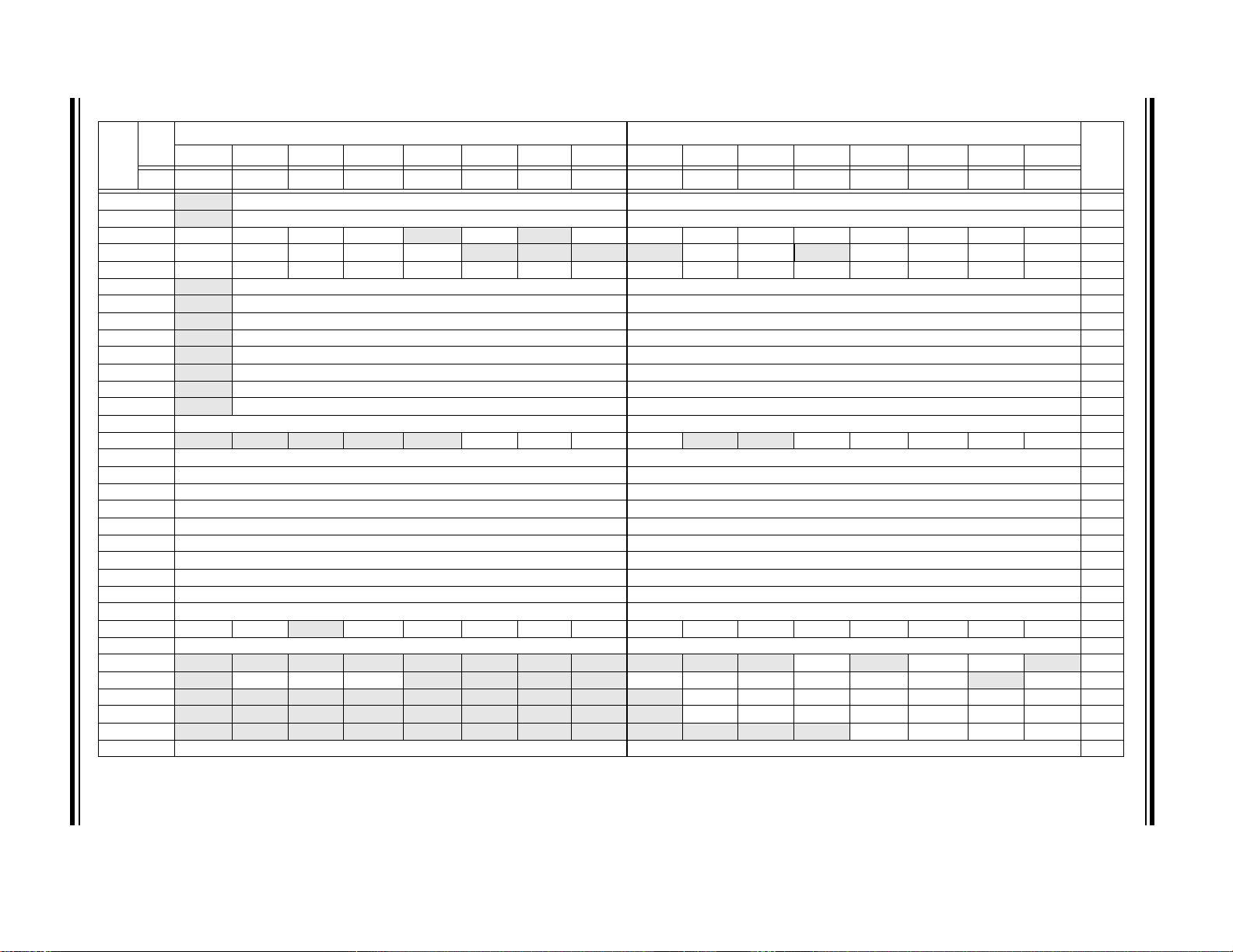
DS39935C-page 26 2010 Microchip Technology Inc.
ENC424J600/624J600
TABLE 3-7: ENC424J600/624J600 REGISTER FILE SUMMARY
8-Bit
File
Name
16-Bit Bit 15 Bit 14 Bit 13 Bit 12 Bit 11 Bit 10 Bit 9 Bit 8 Bit 7 Bit 6 Bit 5 Bit 4 Bit 3 Bit 2 Bit 1 Bit 0
EUDAST — User-Defined Area Start Pointer (EUDAST<14:8>) User-Defined Area Start Pointer (EUDAST<7:0>)
EUDAND — User-Defined Area End Pointer (EUDAND<14:8>) User-Defined Area End Pointer (EUDAND<7:0>)
ESTAT INT FCIDLE RXBUSY CLKRDY r PHYDPX r PHYLNK PKTCNT7 PKTCNT6 PKTCNT5 PKTCNT4 PKTCNT3 PKTCNT2 PKTCNT1 PKTCNT0
EIR CRYPTEN MODEXIF HASHIF AESIF LINKIF r r r r PKTIF DMAIF r TXIF TXABTIF RXABTIF PCFULIF
ECON1 MODEXST HASHEN HASHOP HASHLST AESST AESOP1 AESOP0 PKTDEC FCOP1 FCOP0 DMAST DMACPY DMACSSD DMANOCS TXRTS RXEN
ETXST — TX Start Address (ETXST<14:8>) TX Start Address (ETXST<7:0>)
ETXLEN — TX Length (ETXLEN<14:8>) TX Length (ETXLEN<7:0>)
ERXST — RX Buffer Start Address (ERXST<14:8>) RX Buffer Start Address (ERXST<7:0>)
ERXTAIL — RX Tail Pointer (ERXTAIL<14:8>) RX Tail Pointer (ERXTAIL<7:0>)
ERXHEAD — RX Head Pointer (ERXHEAD<14:8>) RX Head Pointer (ERXHEAD<7:0>)
EDMAST — DMA Start Address (EDMAST<14:8>) DMA Start Address (EDMAST<7:0>)
EDMALEN — DMA Length (EDMALEN<14:8>) DMA Length (EDMALEN<7:0>)
EDMADST — DMA Destination Address (EDMADST<14:8>) DMA Destination Address (EDMADST<7:0>)
EDMACS DMA Checksum, High Byte (EDMACS<15:8>) DMA Checksum, Low Byte (EDMACS<7:0>)
ETXSTAT — — — r r LATECOL MAXCOL EXDEFER DEFER r r CRCBAD COLCNT3 COLCNT2 COLCNT1 COLCNT0
ETXWIRE Transmit Byte Count on Wire (including collision bytes), High Byte (ETXWIRE<15:8>) Transmit Byte Count on Wire (including collision bytes), Low Byte (ETXWIRE<7:0>)
EHT1 Hash Table Filter (EHT1<15:8>) Hash Table Filter (EHT1<7:0>)
EHT2 Hash Table Filter (EHT2<31:24>) Hash Table Filter (EHT2<23:16>)
ETH3 Hash Table Filter (EHT3<47:40>) Hash Table Filter (EHT3<39:32>)
ETH4 Hash Table Filter (EHT4<63:56>) Hash Table Filter (EHT4<55:48>)
EPMM1 Pattern Match Filter Mask (EPMM1<15:8>) Pattern Match Filter Mask (EPMM1<7:0>)
EPMM2 Pattern Match Filter Mask (EPMM2<15:8>) Pattern Match Filter Mask (EPMM2<7:0>)
EPMM3 Pattern Match Filter Mask (EPMM3<15:8>) Pattern Match Filter Mask (EPMM3<7:0>)
EPMM4 Pattern Match Filter Mask (EPMM4<15:8>) Pattern Match Filter Mask (EPMM4<7:0>)
EPMCS Pattern Match Filter Checksum, High Byte (EPMCS<15:8>) Pattern Match Filter Checksum, Low Byte (EPMCS<7:0>)
ERXFCON HTEN MPEN — NOTPM PMEN3 PMEN2 PMEN1 PMEN0 CRCEEN CRCEN RUNTEEN RUNTEN UCEN NOTMEEN MCEN BCEN
EPMO Pattern Match Filter Offset, High Byte (EPMO<15:8>) Pattern Match Filter Offset, Low Byte (EPMO<7:0>)
MACON1 r r — — r r r r — — — LOOPBK r RXPAUS PASSALL r
MACON2 — DEFER BPEN NOBKOFF — — r r PADCFG2 PADCFG1 PADCFG0 TXCRCEN PHDREN HFRMEN r FULDPX
MABBIPG — — — — — — — — — BBIPG6 BBIPG5 BBIPG4 BBIPG3 BBIPG2 BBIPG1 BBIPG0
MAIPG — r r r r r r r — IPG6 IPG5 IPG4 IPG3 IPG2 IPG1 IPG0
MACLCON — — r r r r r r — — — — MAXRET3 MAXRET2 MAXRET1 MAXRET0
MAMXFL MAC Maximum Frame Length, High Byte (MAMXFL<15:8>) MAC Maximum Frame Length, Low Byte (MAMXFL<7:0>)
Legend:
— = unimplemented, read as ‘0’; q = unique MAC address or silicon revision nibble; r = reserved bit, do not modify; x = Reset value unknown. Reset values are shown in hexadecimal for each byte.
High Byte (‘H’ Register) Low Byte (‘L’ Register)
ResetBit 7 Bit 6 Bit 5 Bit 4 Bit 3 Bit 2 Bit 1 Bit 0 Bit 7 Bit 6 Bit 5 Bit 4 Bit 3 Bit 2 Bit 1 Bit 0
00, 00
5F, FF
00, 00
0A, 00
00, 00
00, 00
00, 00
53, 40
5F, FE
53, 40
00, 00
00, 00
00, 00
00, 00
00, 00
00, 00
00, 00
00, 00
00, 00
00, 00
00, 00
00, 00
00, 00
00, 00
00, 00
00, 59
00, 00
x0, 0D
40, B2
00, 12
0C, 12
37, 0F
05, EE

2010 Microchip Technology Inc. DS39935C-page 27
TABLE 3-7: ENC424J600/624J600 REGISTER FILE SUMMARY (CONTINUED)
8-Bit
File
Name
16-Bit Bit 15 Bit 14 Bit 13 Bit 12 Bit 11 Bit 10 Bit 9 Bit 8 Bit 7 Bit 6 Bit 5 Bit 4 Bit 3 Bit 2 Bit 1 Bit 0
MICMD — — — — — — — — — — — — — — MIISCAN MIIRD
MIREGADR — — — r r r r r — — — PHREG4 PHREG3 PHREG2 PHREG1 PHREG0
MAADR3 MAC Address, Byte 6 (MAADR<7:0>) MAC Address, Byte 5 (MAADR<15:8>)
MAADR2 MAC Address, Byte 4 (MAADR<23:16>) MAC Address, Byte 3 (MAADR<31:24>)/OUI Byte 3
MAADR1 MAC Address, Byte 2 (MAADR<39:32>)/OUI Byte 2 MAC Address, Byte 1 (MAADR<47:40>)/OUI Byte 1
MIWR MII Management Write Data, High Byte (MIWR<15:8>) MII Management Write Data, Low Byte (MIWR<7:0>)
MIRD MII Management Read Data, High Byte (MIRD<15:8>) MII Management Read Data, Low Byte (MIRD<7:0>)
MISTAT — — — — — — — — — — — — r NVALID SCAN BUSY
EPAUS Pause Timer Value, High Byte (EPAUS<15:8>) Pause Timer Value, Low Byte (EPAUS<7:0>)
ECON2 ETHEN STRCH TXMAC SHA1MD5 COCON3 COCON2 COCON1 COCON0 AUTOFC TXRST RXRST ETHRST MODLEN1 MODLEN0 AESLEN1 AESLEN0
ERXWM RXFWM7 RXFWM6 RXFWM5 RXFWM4 RXFWM3 RXFWM2 RXFWM1 RXFWM0 RXEWM7 RXEWM6 RXEWM5 RXEWM4 RXEWM3 RXEWM2 RXEWM1 RXEWM0
EIE INTIE MODEXIE HASHIE AESIE LINKIE r r r r PKTIE DMAIE r TXIE TXABTIE RXABTIE PCFULIE
EIDLED LACFG3 LACFG2 LACFG1 LACFG0 LBCFG3 LBCFG2 LBCFG1 LBCFG0 DEVID2 DEVID1 DEVID0 REVID4 REVID3 REVID2 REVID1 REVID0
EGPDATA r r r r r r r r General Purpose Data Window Register
ERXDATA r r r r r r r r Ethernet RX Data Window Register
EUDADATA r r r r r r r r User-Defined Area Data Window Register
EGPRDPT — General Purpose Window Read Pointer, High Byte (ETXRDPT<14:8>) General Purpose Window Read Pointer, Low Byte (ETXRDPT<7:0>)
EGPWRPT — General Purpose Window Write Pointer, High Byte (ETXWRPT<14:8>) General Purpose Window Write Pointer, Low Byte (ETXWRPT<7:0>)
ERXRDPT — RX Window Read Pointer, High Byte (ERXRDPT<14:8>) RX Window Read Pointer, Low Byte (ERXRDPT<7:0>)
ERXWRPT — RX Window Write Pointer, High Byte (ERXWRPT<14:8>) RX Window Write Pointer, Low Byte (ERXWRPT<7:0>)
EUDARDPT — UDA Window Read Pointer (EUDARDPT<14:8>) UDA Window Read Pointer (EUDARDPT<7:0>)
EUDAWRPT — UDA Window Write Pointer (EUDAWRPT<14:8>) UDA Window Write Pointer (EUDAWRPT<7:0>)
Legend:
— = unimplemented, read as ‘0’; q = unique MAC address or silicon revision nibble; r = reserved bit, do not modify; x = Reset value unknown. Reset values are shown in hexadecimal for each byte.
High Byte (‘H’ Register) Low Byte (‘L’ Register)
ResetBit 7 Bit 6 Bit 5 Bit 4 Bit 3 Bit 2 Bit 1 Bit 0 Bit 7 Bit 6 Bit 5 Bit 4 Bit 3 Bit 2 Bit 1 Bit 0
--, 00
01, 00
qq, qq
qq, a3
04, 00
00, 00
00, 00
--, 00
10, 00
CB, 00
10, 0F
80, 10
26, qq
--, xx
--, xx
--, xx
05, FA
00, 00
05, FA
00, 00
05, FA
00, 00
ENC424J600/624J600

ENC424J600/624J600
3.3 PHY Special Function Registers
The PHY registers provide configuration and control of
the PHY module, as well as status information about its
operation. These 16-bit registers are located in their
own memory space, outside of the main SFR space.
Unlike other SFRs, the PHY SFRs are not directly
accessible through the SPI or PSP interfaces. Instead,
access is accomplished through a special set of MAC
control registers that implement a Media Independent
Interface Management (MIIM) defined by IEEE 802.3;
these are the MICMD, MISTAT and MIREGADR
registers.
There are a total of 32 PHY addresses; however, only
10 locations implement user-accessible registers listed
in Table 3-8. Writes to unimplemented locations are
ignored and any attempts to read these locations return
FFFFh. Do not write to reserved PHY register locations
and ignore their content if read.
TABLE 3-8: PHY SPECIAL FUNCTION
REGISTER MAP
Address Name Address Name
00 PHCON1 10
01 PHSTAT1 11 PHCON2
02
03
04 PHANA 14
05 PHANLPA 15
06 PHANE 16
07
08
09
0A
0B
0C
0D
0E
0F
Reserved 12 Reserved
Reserved 13 —
—17Reserved
—18—
—19—
—1A—
—1BPHSTAT2
—1CReserved
—1DReserved
— 1E Reserved
— 1F PHSTAT3
Reserved
Reserved
Reserved
Reserved
3.3.1 READING PHY REGISTERS
When a PHY register is read, the entire 16 bits are
obtained.
To read from a PHY register:
1. Write the address of the PHY register to read
from into the MIREGADR register
(Register 3-1). Make sure to also set reserved
bit 8 of this register.
2. Set the MIIRD bit (MICMD<0>, Register 3-2).
The read operation begins and the BUSY bit
(MISTAT<0>, Register 3-3) is automatically set
by hardware.
3. Wait 25.6 s. Poll the BUSY (MISTAT<0>) bit to
be certain that the operation is complete. While
busy, the host controller should not start any
MIISCAN operations or write to the MIWR
register. When the MAC has obtained the register
contents, the BUSY bit will clear itself.
4. Clear the MIIRD (MICMD<0>) bit.
5. Read the desired data from the MIRD register.
For 8-bit interfaces, the order that these bytes
are read is unimportant.
3.3.2 WRITING PHY REGISTERS
When a PHY register is written to, the entire 16 bits are
written at once; selective bit writes are not
implemented. If it is necessary to reprogram only select
bits in the register, the host microcontroller must first
read the PHY register, modify the resulting data and
then write the data back to the PHY register.
To write to a PHY register:
1. Write the address of the PHY register to write to
into the MIREGADR register. Make sure to also
set reserved bit 8 of this register.
2. Write the 16 bits of data into the MIWR register.
The low byte must be written first, followed by
the high byte.
3. Writing to the high byte of MIWR begins the
MIIM transaction and the BUSY (MISTAT<0>)
bit is automatically set by hardware.
The PHY register is written after the MIIM operation
completes, which takes 25.6 s. When the write operation has completed, the BUSY bit clears itself. The host
controller should not start any MIISCAN, MIWR or
MIIRD operations while the BUSY bit is set.
DS39935C-page 28 2010 Microchip Technology Inc.

ENC424J600/624J600
3.3.3 SCANNING A PHY REGISTER
The MAC can be configured to perform automatic
back-to-back read operations on a PHY register. This
can reduce the host controller complexity when
periodic status information updates are desired.
To perform the scan operation:
1. Write the address of the PHY register to read
from into the MIREGADR register. Make sure to
also set reserved bit 8 of this register.
2. Set the MIISCAN (MICMD<1>) bit. The scan
operation begins and the BUSY (MISTAT<0>)
bit is automatically set by hardware. The first
read operation will complete after 25.6 s. Subsequent reads will be done at the same interval
until the operation is cancelled. The NVALID
(MISTAT<2>) bit may be polled to determine
when the first read operation is complete.
After setting the MIISCAN bit, the MIRD register will
automatically be updated every 25.6 s. There is no
status information which can be used to determine
when the MIRD registers are updated. On the SPI or
8-bit PSP interfaces, the host controller can only read
one register location at a time. Therefore, it must not be
assumed that the values of MIRDL and MIRDH were
read from the PHY at exactly the same time.
When the MIISCAN operation is in progress, the host
controller must not attempt to write to MIWR or start an
MIIRD operation. The MIISCAN operation can be
cancelled by clearing the MIISCAN (MICMD<1>) bit
and then polling the BUSY (MISTAT<0>) bit. New
operations may be started after the BUSY bit is cleared.
REGISTER 3-1: MIREGADR: MII MANAGEMENT ADDRESS REGISTER
U-0 U-0 U-0 R/W-0 R/W-0 R/W-0 R/W-0 R/W-1
— — — r r r r r
bit 15 bit 8
U-0 U-0 U-0 R/W-0 R/W-0 R/W-0 R/W-0 R/W-0
— — — PHREG4 PHREG3 PHREG2 PHREG1 PHREG0
bit 7 bit 0
Legend:
R = Readable bit W = Writable bit U = Unimplemented bit, read as ‘0’
-n = Value at POR ‘1’ = Bit is set ‘0’ = Bit is cleared x = Bit is unknown
bit 15-13 Unimplemented: Read as ‘0’
bit 12-8 Reserved: Write as ‘00001’ (01h)
bit 7-5 Unimplemented: Read as ‘0’
bit 4-0 PHREG<4:0>: MII Management PHY Register Address Select bits
The address of the PHY register which MII Management read and write operations will apply to.
2010 Microchip Technology Inc. DS39935C-page 29

ENC424J600/624J600
REGISTER 3-2: MICMD: MII MANAGEMENT COMMAND REGISTER
U-0 U-0 U-0 U-0 U-0 U-0 U-0 U-0
— — — — — — — —
bit 15 bit 8
U-0 U-0 U-0 U-0 U-0 U-0 R/W-0 R/W-0
— — — — — — MIISCAN MIIRD
bit 7 bit 0
Legend:
R = Readable bit W = Writable bit U = Unimplemented bit, read as ‘0’
-n = Value at POR ‘1’ = Bit is set ‘0’ = Bit is cleared x = Bit is unknown
bit 15-2 Unimplemented: Read as ‘0’
bit 1 MIISCAN: MII Scan Enable bit
1 = PHY register designated by MIREGADR<4:0> is continuously read and the data is copied to MIRD
0 = No MII Management scan operation is in progress
bit 0 MIIRD: MII Read Enable bit
1 = PHY register designated by MIREGADR<4:0> is read once and the data is copied to MIRD
0 = No MII Management read operation is in progress
REGISTER 3-3: MISTAT: MII MANAGEMENT STATUS REGISTER
U-0 U-0 U-0 U-0 U-0 U-0 U-0 U-0
— — — — — — — —
bit 15 bit 8
U-0 U-0 U-0 U-0 R-0 R-0 R-0 R-0
— — — — r NVALID SCAN BUSY
bit 7 bit 0
Legend:
R = Readable bit W = Writable bit U = Unimplemented bit, read as ‘0’
-n = Value at POR ‘1’ = Bit is set ‘0’ = Bit is cleared x = Bit is unknown
bit 15-4 Unimplemented: Read as ‘0’
bit 3 Reserved: Ignore on read
bit 2 NVALID: MII Management Read Data Not Valid Status bit
1 = The contents of MIRD are not valid yet
0 = The MII Management read cycle has completed and MIRD has been updated
bit 1 SCAN: MII Management Scan Status bit
1 = MII Management scan operation is in progress
0 = No MII Management scan operation is in progress
bit 0 BUSY: MII Management Busy Status bit
1 = A PHY register is currently being read or written to
0 = The MII Management interface is Idle
DS39935C-page 30 2010 Microchip Technology Inc.

2010 Microchip Technology Inc. DS39935C-page 31
TABLE 3-9: PHY REGISTER FILE SUMMARY
File Name Bit 15 Bit 14 Bit 13 Bit 12 Bit 11 Bit 10 Bit 9 Bit 8 Bit 7 Bit 6 Bit 5 Bit 4 Bit 3 Bit 2 Bit 1 Bit 0
PHCON1 PRST PLOOPBK SPD100 ANEN PSLEEP r RENEG PFULDPX r r r r r r r r 10, 00
PHSTAT1 r FULL100 HALF100 FULL10 HALF10 r r r r r ANDONE LRFAULT ANABLE LLSTAT rEXTREGS78, 09
PHANA ADNP
PHANLPA LPNP LPACK LPFAULT r LPPAUS1 LPPAUS0 LP100T4 LP100FD LP100 LP10FD LP10 LPIEEE4 LPIEEE3 LPIEEE2 LPIEEE1 LPIEEE0 xx, xx
PHANE r r r r r r r r r r rPDFLTr rLPARCDLPANABL00, 00
PHCON2 r r EDPWRDN r EDTHRES r r r r r r r rFRCLNKEDSTATr 00, 02
PHSTAT2 r r r r r r r r r r rPLRITYr r r r xx, 0x
PHSTAT3 r r r r r r r r r r r SPDDPX2 SPDDPX1 SPDDPX0 r r 00, 40
Legend: r = reserved bit, write as ‘0’; ignore on read; x = unknown. Reset values are shown in hexadecimal for each byte.
rADFAULTr ADPAUS1 ADPAUS0 r AD100FD AD100 AD10FD AD10 ADIEEE4 ADIEEE3 ADIEEE2 ADIEEE1 ADIEE E0 01, E1
Val ue
on
Reset
ENC424J600/624J600

ENC424J600/624J600
Exponent (E)
(up to 1024 bits)
DMA Pointers
Data/Result (X/Y)
(up to 1024 bits)
Modulus (M)
(512, 768 or 1024 bits)
Unimplemented
7800h
787Fh
7880h
78FFh
7900h
797Fh
Data In
(512 bits)
Initialization Vector/State In
(160 bits)
Length State In
(55 bits)
7A00h
7A3Fh
7A40h
7A53h
7A54h
7A5Bh
Digest/State Out
(128 or 160 bits)
7A70h
7A83h
Length State Out (55 bits)
7A84h
7A8Bh
Unimplemented
Encryption Key
(128, 192 or 256 bits)
7C00h
7C1Fh
Text A In/Out (128 bits)
7C20h
7C2Fh
Text B In/Out (128 bits)
7C30h
7C3Fh
XOR Out (128 bits)
7C40h
7C4Fh
Modular ExponentiationMD5/SHA-1 HashAES
General Purpose
Buffer
0000h
5FFFh
Circular RX FIFO
Buffer
ERXST
ERXST – 1
3.4 Cryptographic Data Memory
The cryptographic data memory is used to store key
and data information for the Modular Exponentiation,
AES and MD5/SHA-1 hashing engines. The RAM for
these modules is actually implemented inside of the
modules themselves; this allows fast memory access
for the access-intensive encryption engines, as well as
the simultaneous use of more than one module by an
application. This memory is mapped into an area of
address space that is accessible only by the DMA
controller. The host controller must write to the cryptographic data memory by writing data to the 24-Kbyte
SRAM buffer, then using the DMA to copy it into the
security engine. Reading is performed in the opposite
order, using the DMA to copy the data out of the
security engine and into the SRAM buffer.
The mapping of the cryptographic space is shown in
Figure 3-3. For additional information on the cryptographic engines, refer to Section 15.0 “Cryptographic
Security Engines”. For additional information on the
DMA controller, see Section 14.0 “Direct Memory
Access (DMA) Controller”.
FIGURE 3-3: CRYPTOGRAPHIC DATA
MEMORY MAPPING
3.5 SRAM Buffer
The SRAM buffer is a bulk 12K word x 16-bit (24 Kbytes)
memory, used for TX/RX packet buffering and general
purpose storage by the host microcontroller. In most
cases, the memory is accessed using a byte-oriented
interface, so the memory can normally be thought of as
a simple 24-Kbyte memory buffer divided into a general
purpose/TX area and an RX area (Figure 3-4).
FIGURE 3-4: SRAM BUFFER
ORGANIZATION
DS39935C-page 32 2010 Microchip Technology Inc.
Ethernet communications on 10Base-T and
100Base-TX networks occur at a fixed speed of
10 Mbps or 100 Mbps, respectively. Intra-byte gaps are
not allowed. This requires the host controller to build
outbound transmit frames in their entirety in the SRAM
buffer before the hardware is allowed to begin transmission. Similarly, when receiving packets, the buffer
provides space for the hardware to write the incoming
packet without forcing the host microcontroller to
immediately read and process the packet.
After the part exits Reset, the entire buffer is accessible
by the host controller, regardless of other transmit,
receive or DMA operations that may simultaneously
also be accessing the general purpose or receive
buffer memory.

ENC424J600/624J600
3.5.1 GENERAL PURPOSE BUFFER
The general purpose buffer memory starts at address
0000h and includes all memory up to, but not including,
the memory address pointed to by the ERXST register
(i.e., ERXST – 1).
This buffer can be used to store transmit packets,
received data that the host controller wishes to save for
an extended period, or any type of volatile or state
information that the host controller does not have room
internally to save. Upper layer communications protocols and applications, such as a TCP/IP stack with SSL
or TLS security, are generally infeasible or will perform
poorly over high latency Internet links without using
large buffers.
For reliable, connection oriented protocols like TCP, the
maximum theoretical throughput is directly proportional
to the round trip Acknowledgement latency of the link
and the size of the corresponding transmit or receive
buffer. The general purpose buffer memory on the
ENCX24J600 is well suited for use by TCP for
implementing high-performance communications
across the Internet, where round trip Acknowledgement
latency is in the order of many milliseconds.
3.5.2 RECEIVE BUFFER
The receive buffer constitutes a circular FIFO buffer
managed by hardware. The buffer extends inclusively
from the byte pointed to by the ERXST Pointer, to the
very end of the SRAM at address 5FFFh. The size of
the buffer, in bytes, is therefore defined as:
RX Buffer Size = 5FFFh – ERXST + 1
As bytes of data are received from the Ethernet
interface, they are written into the receive buffer
sequentially. However, after the memory at address
5FFFh is written to, the hardware will automatically
wrap around and write the next byte of received data to
the ERXST address. As a result, the receive hardware
will never write outside the boundaries of the RX FIFO
buffer.
For proper 16-bit word alignment, the ERXST Pointer is
required to point to an even memory address. The
Least Significant bit of this register is read-only and
fixed as ‘0’ to force even alignment. All other
implemented bits in this register are read/write and can
be programmed by software to point to any even
address, from 0000h to 5FFEh.
The default value of ERXST on device Reset is 5340h.
This allocates 21,312 bytes to the general purpose
buffer and 3,264 bytes to the RX buffer. This RX buffer
size is adequate to store at least two maximum length
Ethernet frames, or any combination of numerous
smaller packets.
The host controller may only program the ERXST
Pointer when the receive logic is disabled. The pointer
must not be modified while the receive logic is enabled
by having RXEN (ECON1<0>) set.
The receive memory is always accessible to the RX
hardware, regardless of transmit, DMA operations or
host controller read/write operations, which may be
accessing the SRAM simultaneously. The RX
hardware will never drop a packet due to insufficient
memory access bandwidth.
3.5.3 TRANSMIT BUFFER
The ENC624J600 family does not implement a dedicated transmit buffer. The transmit hardware has the
flexibility of transmitting data starting at any memory
address, including odd memory addresses which are
off of a 16-bit word boundary. The host controller can
transmit data from either the general purpose area or
RX FIFO area of the entire 24 Kbytes of SRAM.
Because of the transmit flexibility, the host controller may
store many prebuilt packets in the general purpose
buffer for quick transmission. Alternatively, because the
hardware can transmit data from the receive buffer, it is
possible to quickly modify certain packet header fields
and retransmit received packets without reading the
entire packet contents into the host microcontroller. This
feature may improve performance on certain proxy,
gateway or echoing (“ping”) applications.
The transmit hardware performs reads from the SRAM
only; it never writes anything into the SRAM.
The entire SRAM is always accessible to the TX
hardware, regardless of the receive activity, DMA
operations or host controller read/write operations,
which may be simultaneously attempting to access the
SRAM.
3.5.4 DIRECT SRAM BUFFER ACCESS
When one of the PSP interfaces is used, the SRAM
buffer is directly accessible through the interface.
Assuming that all necessary address lines are connected, all addresses in the memory maps shown in
Figure 3-2 (except for the cryptographic data memory)
may be directly read and written to. When accessed
through this manner, the host controller must handle all
address increment and wrap-around calculations that
may be necessary. This also includes translation from
byte to word addressing when a 16-bit PSP interface is
used.
Direct access is unavailable when the SPI interface is
used.
2010 Microchip Technology Inc. DS39935C-page 33

ENC424J600/624J600
General Purpose
Buffer
0000h
5FFFh
Circular RX FIFO
Buffer
ERXST
ERXST – 1
EGPRDPT
EGPWRPT
ERXRDPT
ERXWRPT
EUDARDPT
EUDAWRPT
EUDAST
EUDAND
EGPDATA
ERXDATA
EUDADATA
EGPDATA
ERXDATA
EUDADATA
EUDADATA
EGPDATA
ERXDATA
Unimplemented
Read
Write
Read
Write
Read
Write
Data Windows
Buffer Pointers
3.5.5 INDIRECT SRAM BUFFER ACCESS
Indirect access to the SRAM buffer is available to all I/O
interfaces. For the SPI interface, it is the only method
available. For PSP interfaces, it may be used in
addition to the direct access method.
Three separate pointer pairs are available for the host
microcontroller to use when accessing the SRAM:
• General Purpose Buffer Read/Write Pointer
(EGPRDPT/EGPWRPT)
• Receive Buffer Read/Write Pointer
(ERXRDPT/ERXWRPT)
• User-Defined Area Read/Write Pointer
(EUDARDPT/EUDAWRPT)
Each of these pointer pairs provides an 8-bit virtual
window register (EGPDATA, ERXDATA and EUDATA)
through which the SRAM data is read or written. The
EGPDATA, ERXDATA and EUDADATA are all 8 bits
wide. When writing to them using a 16-bit PSP
interface, the low-order byte select or write enable must
be used; strobing the high byte Byte Select or Write
Enable has no effect. When reading from a 16-bit PSP
interface, one byte of useful data will be returned on the
lower 8 bits of the data bus; the upper 8 bits are to be
ignored.
When a data window register is read, the memory
contents at the address indicated by the corresponding
Read Pointer are obtained and presented to the host
microcontroller. Similarly, when a data window register
is written, the memory contents at the address
indicated by the corresponding Write Pointer are
updated by the data from the host microcontroller.
Following a read/write operation, the appropriate
pointer is automatically incremented in hardware.
pointers and their associated data windows are shown
in Figure 3-5.
FIGURE 3-5: POINTERS FOR INDIRECT BUFFER ACCESS
DS39935C-page 34 2010 Microchip Technology Inc.

ENC424J600/624J600
General Purpose
Buffer
0000h
5FFFh
Circular RX FIFO
Buffer
ERXST
ERXST – 1
Unimplemented
if EGPRDPT/EGPWRPT = ERXST – 1, then
EGPRDPT/EGPWRPT = 0000h
else if EGPRDPT/EGPWRPT = 5FFFh, then
EGPRDPT/EGPWRPT = 0000h
else
EGPRDPT/EGPWRPT = EGPRDPT/EGPWRPT + 1
For example, to read data from address 5402h of the
buffer:
1. Write 5402h to EGPRDPT.
2. Read from EGPDATA.
Following the read, the EGPRDPT value normally
increments by 1 (to 5403h in this example). If the host
subsequently wants to read from address 5403h, it can
simply perform a second read from the EGPDATA
Window register. The Write Pointer, EGPWRPT, is not
affected by the read operation.
Similarly, to write A3h to address 0007h of the buffer:
1. Write 0007h to EGPWRPT.
2. Write A3h to EGPDATA.
Following the write, the EGPWRPT value normally
increments by 1 (to 0008h in this example). The Read
Pointer, EGPRDPT, is not affected by the write
operation.
Each of the three pointer sets (general purpose,
receive and user-defined area) can be used to access
any address within the SRAM buffer. They differ from
each other based on their address wrapping behavior.
Applications may choose to use all three pointer
interfaces to access the RAM. This may offer maximum
application performance as it will require minimal context switching overhead when, for example, switching
from reading a received packet to reading from general
purpose RAM. However, for simplicity, some
applications may prefer to use only one or two of the
three E*DATA interfaces.
3.5.5.1 Circular Wrapping with EGPDATA
Normally, operations involving EGPDATA cause the
EGPRDPT or EGPWRPT Pointer to automatically
increment by one byte address. However, if the end of
the general purpose buffer area (ERXST – 1) is
reached, or the end of the implemented SRAM (5FFFh)
is reached, the pointer will increment to address 0000h
instead, causing subsequent accesses to wrap around
to the beginning of the SRAM buffer (Figure 3-6). The
increment behavior logic is explained in Equation 3-1.
FIGURE 3-6: CIRCULAR BUFFER
WRAPPING USING THE
EGPDATA WINDOW
EQUATION 3-1: POINTER INCREMENT LOGIC FOR EGPRDPT AND EGPWRPT
2010 Microchip Technology Inc. DS39935C-page 35

ENC424J600/624J600
General Purpose
Buffer
0000h
5FFFh
Circular RX FIFO
Buffer
ERXST
ERXST – 1
Unimplemented
if ERXRDPT/ERXWRPT = 5FFFh, then
ERXRDPT/ERXWRPT = ERXST
else
ERXRDPT/ERXWRPT = ERXRDPT/ERXWRPT + 1
if EUDARDPT/EUDAWRPT = EUDAND, then
EUDARDPT/EUDAWRPT = EUDAST
else if EUDARDPT/EUDAWRPT = 5FFFh, then
EUDARDPT/EUDAWRPT = 0000h
else
EUDARDPT/EUDAWRPT = EUDARDPT/EUDAWRPT + 1
3.5.5.2 Circular Wrapping with ERXDATA
As with the general purpose pointers, operations with
ERXDATA normally cause the ERXRDPT or
ERXWRPT Pointer to automatically increment by one
byte address. However, if the end of the receive buffer
area (5FFFh) is reached, the pointer will increment to
the start of the receive FIFO buffer area instead, as
defined by ERXST (Figure 3-7).
The receive wrapping rules for the ERXDATA interface
are identical to the buffer wrapping rules used by the
receive hardware. Therefore, this register interface is
ideally suited to reading packet data from the receive
buffer. The host controller can set the ERXRDPT value
at the start of a packet in the receive buffer and sequentially read out the entire packet contents without having
to write to the ERXRDPT Read Pointer again.
FIGURE 3-7: CIRCULAR BUFFER
WRAPPING USING THE
ERXDATA WINDOW
EQUATION 3-2: POINTER INCREMENT LOGIC FOR ERXRDPT AND ERXWRPT
3.5.5.3 Circular Wrapping with EUDADATA
The user-defined buffer area is primarily useful for
setting up a circular FIFO within the general purpose
area for use by TCP/IP stacks or other applications. The
wrap-around behavior of the user-defined buffer area is
somewhat more complicated than with the general
purpose or receive buffer cases. This is because the
user-definable boundaries set by EUDAST and
EUDAND take priority over normal wrapping behavior.
Like other pointers, EUDAST and EUDAND are fully
user-configurable from the host microcontroller. Unlike
ERXST, which must not be modified while the receive
hardware is enabled, EUDAST and EUDAND can be
modified at any time.
As in the previous instances, operations with
EUDADATA normally cause the EUDARDPT or
EUDAWRPT Pointer to automatically increment by one
byte address. If the value in EUDAND is reached, the
pointer will increment to the address specified by
EUDAST instead. However, if the end of memory
(5FFFh) is reached, and EUDAND is located at some
other address, the pointer will increment to the beginning of memory (0000h). If EUDAND is set to 5FFFh,
the pointer address increments to the value of
EUDAST, instead of 0000h.
The increment behavior logic is explained in
Equation 3-3.
EQUATION 3-3: POINTER INCREMENT LOGIC FOR EUDARDPT AND EUDAWRPT
DS39935C-page 36 2010 Microchip Technology Inc.

ENC424J600/624J600
General Purpose
Buffer
0000h
5FFFh
Circular RX FIFO
Buffer
Unimplemented
EUDAST
EUDAND
General Purpose
Buffer
0000h
5FFFh
Circular RX FIFO
Buffer
Unimplemented
EUDAST
EUDAND
General Purpose
Buffer
0000h
5FFFh
Circular RX FIFO
Buffer
Unimplemented
EUDAST
EUDAND
Case 1:
EUDAND > EUDAST
Case 2:
EUDAST > EUDAND
Case 3:
EUDAST and EUDAND > 5FFFh
User-Defined Buffer Disabled
User-Defined Buffer with
“Exclusion Zone”
Normal User-Defined Buffer
Excluded
User-Defined
Buffer
The user-defined area start address, EUDAST, is a
read/write register. For wrapping to work correctly, the
hardware enforces 16-bit even word alignment of this
register by internally having the Least Significant bit
tied off to ‘0’. Similarly, the user-defined area end
address, EUDAND, is a read/write register that is
forced to an odd memory address. The Least Significant bit of EUDAND is internally tied to ‘1’. Applications
wishing to set up general purpose circular FIFOs in
memory using these hardware features must observe
these same alignment requirements.
If the user-defined area end address, EUDAND, is at a
higher memory address relative to the start address,
EUDAST, the buffer wraps to either EUDAST or the
beginning of memory, depending on where the
EUDARDPT or EUDAWRPT Pointers are located. This
is shown in Case 1 of Figure 3-8.
In some cases (for example, when accessing
fragmented data), it may be useful to place the
EUDAST Pointer at a higher memory address relative
user-defined area pointers will jump over the range of
addresses between EUDAND and EUDAST. This is
shown in Case 2.
If the user-defined buffer is not needed, it can
effectively be disabled by setting EUDAST and
EUDAND to addresses outside of the implemented
memory area. For example, if EUDAST is set to 6000h
and EUDAND is set to 6001h, EUDARDPT and
EUDAWRPT will never reach these addresses.
Instead, they wrap from the end of implemented RAM
to its beginning, as shown in Case 3.
When the user-defined buffer is disabled, the host controller can use the EUDADATA interface as a second
general purpose window into RAM. Unlike the original
general purpose pointers, however, EUDARDPT and
EUDAWRPT do not wrap at the ERXST boundary,
thereby allowing access to the full SRAM buffer area.
This may be beneficial for debugging and testing
purposes where it may be desirable to read or write the
entire SRAM buffer in a single operation.
to the end address. When organized in such a manner,
an “exclusion zone” in the middle of the memory range
is created; sequential read/write operations with the
FIGURE 3-8: CIRCULAR BUFFER WRAPPING USING THE EUDATA WINDOW
2010 Microchip Technology Inc. DS39935C-page 37

ENC424J600/624J600
NOTES:
DS39935C-page 38 2010 Microchip Technology Inc.

ENC424J600/624J600
4.0 SERIAL PERIPHERAL
INTERFACE (SPI)
ENC424J600/624J600 devices implement an optional
SPI I/O port for applications where a parallel microcontroller interface is not available or is undesirable. An
SPI port is commonly available on many microcontrollers, and can be simulated in software on regular
I/O pins where it is not implemented. This makes the
SPI port ideal for using ENC424J600/624J600 devices
with the widest possible range of host controllers.
4.1 Physical Implementation
The SPI port on ENC424J600/624J600 devices
operates as a slave port only. The host controller must
be configured as an SPI master that generates the
Serial Clock (SCK) signal.
This implementation supports SPI Mode 0,0, which
requires:
• SCK is Idle at a logic low state
• Data is clocked in on rising clock edges and
changes on falling clock edges
Other SPI modes that use inverted clock polarity and/or
phase are not supported.
Commands and data are sent to the device on the SI
pin. Data is driven out on the SO line on the falling edge
of SCK. The CS
operation is performed, and returned to logic high when
finished.
When CS
is set to a high-impedance state and becomes 5V tolerant. This allows the ENCX24J600 to be connected to a
single SPI bus shared by multiple SPI slave devices
that also go to a high-impedance state when inactive.
For details on the physical connections to the interface,
see Section 2.7 “Host Interface Pins”.
is in the inactive (logic high) state, the SO pin
pin must be held low while any
4.2 SPI Instruction Set
The SPI interface supports a unique instruction set,
consisting of 47 distinct opcodes. These include a large
number of optimized opcodes that perform a wide
range of frequently performed operations with a mini-
mum of SPI protocol overhead. Complete Ethernet
functionality can be achieved with as few as six N-byte
opcodes. The use of the other 41 is optional; however,
doing so will generally improve overall system
performance.
The SPI opcodes are divided into four families:
• Single Byte: Direct opcode instructions; designed
for task-oriented SFR operations with no data
returned
• Two-Byte: Direct opcode instruction; designed for
SFR operation with byte data returned
• Three-Byte: Opcode with word length argument;
includes read and write operations, designed for
pointer manipulation with word length data
returned
• N-Byte: Opcode with one or more bytes of
argument; includes read and write operations
designed for general memory space access with
one or more bytes of data returned
A complete summary of all opcodes is provided in
Table 4-1. A detailed explanation of each opcode family
follows.
2010 Microchip Technology Inc. DS39935C-page 39

ENC424J600/624J600
TABLE 4-1: SPI INSTRUCTION SET
Instruction Mnemonic
1st Byte 2nd Byte 3rd Byte Nth Byte
Bank 0 Select B0SEL 1100 0000
Bank 1 Select B1SEL 1100 0010 — — —
Bank 2 Select B2SEL 1100 0100
Bank 3 Select B3SEL 1100 0110
System Reset SETETHRST 1100 1010 — — —
Flow Control Disable FCDISABLE 1110 0000 — — —
Flow Control Single FCSINGLE 1110 0010 — — —
Flow Control Multiple FCMULTIPLE 1110 0100 — — —
Flow Control Clear FCCLEAR 1110 0110 — — —
Decrement Packet Counter SETPKTDEC 1100 1100 — — —
DMA Stop DMASTOP 1101 0010 — — —
DMA Start Checksum DMACKSUM 1101 1000 — — —
DMA Start Checksum with Seed DMACKSUMS 1101 1010 — — —
DMA Start Copy DMACOPY 1101 1100 — — —
DMA Start Copy and Checksum with Seed DMACOPYS 1101 1110
Request Packet Transmission SETTXRTS 1101 0100 — — —
Enable RX ENABLERX 1110 1000 — — —
Disable RX DISABLERX 1110 1010 — — —
Enable Interrupts SETEIE 1110 1100 — — —
Disable Interrupts CLREIE 1110 1110 — — —
Read Bank Select RBSEL 1100 1000 xxxx xxxx — —
Write EGPRDPT WGPRDPT 0110 0000 dddd dddd DDDD DDDD —
Read EGPRDPT RGPRDPT 0110 0010 xxxx xxxx XXXX XXXX —
Write ERXRDPT WRXRDPT 0110 0100 dddd dddd DDDD DDDD —
Read ERXRDPT RRXRDPT 0110 0110 xxxx xxxx XXXX XXXX —
Write EUDARDPT WUDARDPT 0110 1000 dddd dddd DDDD DDDD —
Read EUDARDPT RUDARDPT 0110 1010 xxxx xxxx XXXX XXXX —
Write EGPWRPT WGPWRPT 0110 1100 dddd dddd DDDD DDDD —
Read EGPWRPT RGPWRPT 0110 1110 xxxx xxxx XXXX XXXX —
Write ERXWRPT WRXWRPT 0111 0000 dddd dddd DDDD DDDD —
Read ERXWRPT RRXWRPT 0111 0010 xxxx xxxx XXXX XXXX —
Write EUDAWRPT WUDAWRPT 0111 0100 dddd dddd DDDD DDDD —
Read EUDAWRPT RUDAWRPT 0111 0110 xxxx xxxx XXXX XXXX —
Read Control Register RCR 000a aaaa xxxx xxxx XXXX XXXX XXXX XXXX
Write Control Register WCR 010a aaaa dddd dddd DDDD DDDD DDDD DDDD
Read Control Register Unbanked RCRU 0010 0000 AAAA AAAA xxxx xxxx XXXX XXXX
Write Control Register Unbanked WCRU 0010 0010 AAAA AAAA dddd dddd DDDD DDDD
Bit Field Set BFS 100a aaaa dddd dddd DDDD DDDD DDDD DDDD
Bit Field Clear BFC 101a aaaa dddd dddd DDDD DDDD DDDD DDDD
Bit Field Set Unbanked BFSU 0010 0100 AAAA AAAA dddd dddd DDDD DDDD
Bit Field Clear Unbanked BFCU 0010 0110 AAAA AAAA dddd dddd DDDD DDDD
Read EGPDATA RGPDATA 0010 1000 xxxx xxxx XXXX XXXX XXXX XXXX
Write EGPDATA WGPDATA 0010 1010 dddd dddd DDDD DDDD DDDD DDDD
Read ERXDATA RRXDATA 0010 1100 xxxx xxxx XXXX XXXX XXXX XXXX
Write ERXDATA WRXDATA 0010 1110 dddd dddd DDDD DDDD DDDD DDDD
Read EUDADATA RUDADATA 0011 0000 xxxx xxxx XXXX XXXX XXXX XXXX
Write EUDADATA WUDADATA 0011 0010 dddd dddd DDDD DDDD DDDD DDDD
Legend: x/X = read data, d/D = write data, a = banked SFR address, A = unbanked SFR address. ‘X’ and ‘D’ are optional.
Instruction
— — —
— — —
— — —
— — —
DS39935C-page 40 2010 Microchip Technology Inc.

ENC424J600/624J600
CS
SCK
SI
SO x x x x x x x xHi-Z Hi-Zx
1 2 3 4 5 6 7 8
Opcode
1 1 c5 c4 c3 c2 c1 0
4.3 Single Byte Instructions
All single byte instructions are designed to perform a
simple command that affects the ENCX24J600
device’s state. In most cases, they set or clear a small
number of control bits which would otherwise require
one or more N-byte opcodes to perform. None of these
instructions return any data to the host microcontroller.
Figure 4-1 shows the timing relationships for performing
a single byte operation. The opcode (‘11xxxxx0’) is
presented on the device’s SI pin starting with the Most
Significant bit of the opcode; the Least Significant bit is
always ‘0’. The SO pin is actively driven with
indeterminate ‘1’s or ‘0’s while the CS
It continues to be driven until the CS
Because all single byte instructions are fixed length
with no optional parameters, it is possible to execute
any instruction immediately following the execution of
any single byte instruction without deasserting the chip
select line in between.
If the CS
of the opcode is sent to the ENCX24J600, indeterminate
results will occur. In some cases, the instruction is
executed or partially executed. To avoid this, it is recommended that a single byte instruction should not be
interrupted. If it is unavoidable that an instruction gets
partially executed, have the application later reissue the
same instruction and let it complete to place the device
into a known state.
There are a total of 20 single byte opcodes, which are
listed in Table 4-2. All single byte opcodes will operate
regardless of which SFR bank is selected at the time.
Those opcodes that affect multiple bits, or affect SFR
addressing, are detailed below.
control signal is deactivated before the 8th bit
pin is driven low.
pin is returned high.
4.3.1 BxSEL OPCODES
The bank select opcodes, B0SEL, B1SEL, B2SEL and
B3SEL, switch the SFR bank to Bank 0, Bank 1, Bank 2
or Bank 3, respectively. The updated bank select state
is saved internally inside the ENCX24J600 in volatile
memory. Firmware can retrieve the currently selected
SFR bank state by using the Read Bank Select
(RBSEL) opcode.
The bank select opcodes are needed to access most
SFR addresses when using the RCR, WCR, BFS and
BFC instructions. These are discussed in more detail in
Section 4.6 “N-Byte Instructions”.
Upon device power-up or System Reset, Bank 0 is
automatically selected. After Reset, hardware does not
modify the bank state again. Any value programmed by
a BxSEL opcode is retained until the next BxSEL
opcode is executed or a System Reset is issued.
4.3.2 FC (FLOW CONTROL) OPCODES
The flow control opcodes, FCDISABLE, FCSINGLE,
FCMULTIPLE and FCCLEAR, all modify the device’s
Flow Control mode by changing the values of the
FCOP<1:0> bits (ECON1<7:6>). These opcodes
execute regardless of the currently selected SFR bank.
For more information on flow control operation, see
Section 11.0 “Flow Control”.
4.3.3 DMA OPCODES
The DMA opcodes, DMASTOP, DMACKSUM, DMACKSUMS,
DMACOPY and DMACOPYS, modify the operation of the
device’s DMA controller, all by simultaneously changing
the values of the DMAST, DMACPY, DMACSSD and
DMANOCS control bits (ECON1<5:2>). For more information on DMA operation, see Section 14.0 “Direct
Memory Access (DMA) Controller”.
FIGURE 4-1: SINGLE BYTE INSTRUCTION TIMING
2010 Microchip Technology Inc. DS39935C-page 41
ENC424J600/624J600
CS
SCK
SI
SO x x x x x x x xHi-Z Hi-Zx0
0 1 0 0
d d
0
1 2 3 4 5 6 7 8 9 10 11 12 13 14 15 16
RBSEL Opcode
SFR Bank Select
1 01
0 0 0 00
TABLE 4-2: SINGLE BYTE INSTRUCTIONS
Mnemonic Opcode Instruction
B0SEL 1100 0000 Selects SFR Bank 0
B1SEL 1100 0010 Selects SFR Bank 1
B2SEL 1100 0100 Selects SFR Bank 2
B3SEL 1100 0110 Selects SFR Bank 3
SETETHRST 1100 1010 Issues System Reset by setting ETHRST (ECON2<4>)
FCDISABLE 1110 0000 Disables flow control (sets ECON1<7:6> = 00)
FCSINGLE 1110 0010 Transmits a single pause frame (sets ECON1<7:6> = 01)
FCMULTIPLE 1110 0100 Enables flow control with periodic pause frames (sets ECON1<7:6> = 10)
FCCLEAR 1110 0110 Terminates flow control with a final pause frame (sets ECON1<7:6> = 11)
SETPKTDEC 1100 1100 Decrements PKTCNT by setting PKTDEC (ECON1<8>)
DMASTOP 1101 0010 Stops current DMA operation by clearing DMAST (ECON1<5>)
DMACKSUM 1101 1000 Starts DMA and checksum operation (sets ECON1<5:2> = 1000)
DMACKSUMS 1101 1010 Starts DMA checksum operation with seed (sets ECON1<5:2> = 1010)
DMACOPY 1101 1100 Starts DMA copy and checksum operation (sets ECON1<5:2> = 1100)
DMACOPYS 1101 1110 Starts DMA copy and checksum operation with seed (sets ECON1<5:2> = 1110)
SETTXRTS 1101 0100 Sets TXRTS (ECON1<1>), sends an Ethernet packet
ENABLERX 1110 1000 Enables packet reception by setting RXEN (ECON1<0>)
DISABLERX 1110 1010 Disables packet reception by clearing RXEN (ECON1<0>)
SETEIE 1110 1100 Enable Ethernet Interrupts by setting INT (ESTAT<15>)
CLREIE 1110 1110 Disable Ethernet Interrupts by clearing INT (ESTAT<15>)
4.4 Two-Byte Instructions
There is only one instruction in the ENCX24J600 command set which uses two SPI bytes. The Read Bank
Select opcode, RBSEL, reads the internal SFR bank
select state and returns the value to the host controller.
Figure 4-2 shows the timing relationships for performing the two-byte operation. The first byte of the opcode
(‘11001000’) must be presented on the SI pin, MSb
first, followed by “don’t care” values for the second byte
th
through 16th SCK rising edges). The bank select
(9
value (00h through 03h) is returned on the SO pin, MSb
first, while the second byte is being presented on the SI
pin.
Because this instruction is a fixed length with no
optional parameters, it is possible to execute any
instruction following the execution of RBSEL without
deasserting the chip select line in between.
Since this opcode does not modify the ENCX24J600
internal state, it can be aborted at any time by returning
the CS
pin to the inactive state.
FIGURE 4-2: TWO-BYTE INSTRUCTION TIMING (RBSEL OPCODE)
DS39935C-page 42 2010 Microchip Technology Inc.
ENC424J600/624J600
CS
SCK
SI
SO x x x x x x x xHi-Z Hi-ZxD7 D6 D5
1 10 c4 c3 c2 1
d7 d6 d5 d4 d3 d2 d1 d0 D4 D3 D2 D1 D0
0
1 2 3 4 5 6 7 8 9 10 11 12 13 14 15 16 17 18 19 20 21 22 23 24
Opcode
Read Low Byte
Read High Byte
(optional)
CS
SCK
SI
SO x x x x x x x xHi-Z
d5 d4 d3 d2 d1
Hi-Zx
d6d7 d0
x x x
D01 10 c4 c3 c2 0 D7 D6 D5 D4 D3 D2 D1
x x x x x x x x x x x x x
0
1 2 3 4 5 6 7 8 9 10 11 12 13 14 15 16 17 18 19 20 21 22 23 24
Opcode Write Low Byte
Write High Byte
(optional)
4.5 Three-Byte Instructions
All three-byte instructions are designed to quickly read
or update the Read and Write Pointers used to access
the SRAM buffer area. Unlike the single byte instructions and RBSEL, each instruction in this group has
distinct read and write implementations.
For read commands (shown in Figure 4-3), the opcode
byte (‘011xxx10’) must be presented on the SI pin,
MSb first, followed by “don’t care” values for the second
and third bytes (9
Response data is returned on the SO line during the
second and third bytes.
Data on the SO line is also presented in MSb first bit
ordering. However, read commands are intended to
read a 16-bit pointer in little-endian byte ordering.
Therefore, the first byte on the SO line (returned during
SCK clocks, 9 through 16) is the lower byte of the 16-bit
pointer and is followed by the upper byte (returned
during SCK clocks 17 through 24).
Read operations do not affect the ENCX24J600
device’s internal state, and therefore, can be aborted at
any time by deasserting chip select.
th
through 24th SCK rising edges).
For write commands (shown in Figure 4-4), the opcode
byte (‘011xxx00’) must be presented on the SI line,
MSb first, followed immediately by the pointer data to
be written. Like the data returned during a read
operation, the write data must be presented MSb first,
Least Significant Byte first.
If the application only needs to write to the lower byte of
a 16-bit pointer, it can optionally skip the upper byte by
raising chip select after the 16
adequate chip select hold time to elapse. The hardware
would then update the lower byte of the pointer while
maintaining the original value in the upper byte.
During write operations, the device actively drives the
SO line while the chip select line is active. The value
during this interval is to be ignored.
All three-byte instructions, including read operations,
are considered to be finished at the end of the 24th
SCK clock (if reached). The host controller may issue
another SPI instruction or multiple fixed length
instructions without deasserting chip select.
There are 12 three-byte instructions, which are divided
equally between read and write instructions. They are
listed in Table 4-3.
FIGURE 4-3: THREE-BYTE READ INSTRUCTION TIMING
th
clock pulse and allowing
FIGURE 4-4: THREE-BYTE WRITE INSTRUCTION TIMING
2010 Microchip Technology Inc. DS39935C-page 43

ENC424J600/624J600
TABLE 4-3: THREE-BYTE INSTRUCTIONS
Mnemonic
WGPRDPT 0110 0000 dddd dddd DDDD DDDD Write General Purpose Buffer Read Pointer
RGPRDPT 0110 0010 xxxx xxxx XXXX XXXX Read General Purpose Buffer Read Pointer
WRXRDPT 0110 0100 dddd dddd DDDD DDDD Write Receive Buffer Read Pointer (ERXRDPT).
RRXRDPT 0110 0110 xxxx xxxx XXXX XXXX Read Receive Buffer Read Pointer (ERXRDPT).
WUDARDPT 0110 1000 dddd dddd DDDD DDDD Write User-Defined Area Read Pointer (EUDARDPT).
RUDARDPT 0110 1010 xxxx xxxx XXXX XXXX Read User-Defined Area Read Pointer (EUDARDPT).
WGPWRPT 0110 1100 dddd dddd DDDD DDDD Write General Purpose Buffer Write Pointer
RGPWRPT 0110 1110 xxxx xxxx XXXX XXXX Read General Purpose Buffer Write Pointer
WRXWRPT 0111 0000 dddd dddd DDDD DDDD Write Receive Buffer Write Pointer (ERXWRPT).
RRXWRPT 0111 0010 xxxx xxxx XXXX XXXX Read Receive Buffer Write Pointer (ERXWRPT).
WUDAWRPT 0111 0100 dddd dddd DDDD DDDD Write User-Defined Area Write Pointer (EUDAWRPT).
RUDAWRPT 0111 0110 xxxx xxxx XXXX XXXX Read User-Defined Area Write Pointer (EUDAWRPT).
Legend: x/d = pointer data (LSB), X/D = pointer data (MSB, optional).
Opcode Argument
Instruction
1st Byte 2nd Byte 3rd Byte
(EGPRDPT).
(EGPRDPT).
(EGPWRPT).
(EGPWRPT).
DS39935C-page 44 2010 Microchip Technology Inc.

ENC424J600/624J600
CS
SCK
SI
SO x x x x x x x xHi-Z
d5 d4 d3 d2 d1d6d7 d0
x x x
D0a4 a3 a2 D7 D6 D5 D4 D3 D2 D1
x x x x x x x x x x x x x
1 2 3 4 5 6 7 8 9 10 11 12 13 14 15 16 17 18 19 20 21 22 23 24
Opcode w/SFR Address
Write 1st Byte
Write 2nd Byte
(optional)
25 26 27
D7 D6 D5
x x x
Additional
c7 c6 c5 a1 a0
CS
SCK
SI
SO x x x x x x x x
Hi-Z
D7 D6 D5
a4 a3 a2
d7 d6 d5 d4 d3 d2 d1 d0 D4 D3 D2 D1 D0
1 2 3 4 5 6 7 8 9 10 11 12 13 14 15 16 17 18 19 20 21 22 23 24
Read 1st Byte
Read 2nd Byte
(optional)
25 26 27
D7 D6 D5
Additional
c7 c6 c5 a1 a0
Opcode w/SFR Address
Write Operation
Read Operation
4.6 N-Byte Instructions
N-byte instructions make up the most versatile class of
SPI commands, as they can read or write to any
addressable SFR or SRAM space. Their name comes
from their variable length nature; they require a minimum of two bytes, but can take an indefinite number of
bytes of data argument, or return an unlimited number
of output bytes. This makes them useful for reading or
writing entire arrays of data to or from the SRAM buffer.
Since these instructions are of an intrinsically variable
length, no other opcode may follow any N-byte
instruction until the CS
high terminates the instruction and then places the SO
pin in a high-impedance state.
The format of the N-byte instructions differs depending
on if a read versus a write command is executed, and
if a banked SFR, unbanked SFR or SRAM location is
accessed. The differences are discussed in the
following sections.
4.6.1 BANKED SFR OPERATION
The N-byte Banked SFR instructions are WCR, RCR, BFS
and BFC. These instructions depend on the use of the
appropriate BxSEL instructions to select the proper SFR
line is driven high. Driving CS
bank prior to their execution. Because of this, they
cannot be used for the unbanked SFR space (80h
through 9Fh).
Figure 4-5 shows the timing relationships for these
operations. Like all other opcodes, data must be
presented on the SI pin, MSb first. For all banked
instructions, the first byte of data must be the opcode,
comprised of a 3-bit prefix designating the instruction
and a 5-bit banked SFR address. If the instruction is a
write or bit field set/clear opcode, the next bytes are the
data or bit mask to be written. For read instructions, the
next bytes on the SI pin are “don’t care”.
For write and bit field set/clear instructions, the SO pin
is actively driven with indeterminate ‘1’s or ‘0’s while
pin is driven low. For read instructions, indeter-
the CS
minate data is clocked out on SO during SCK clocks,
1 through 8. Starting with the 9th clock, valid data is
clocked out byte-wise on SO, MSb first.
As long as the CS
pin is held low, clocks on SCK are
provided and data is presented on SI, the instruction
continues to execute indefinitely, automatically incrementing to the next register address in the SFR Bank
and writing data from SI to, or outputting data on SO
from, subsequent registers. When the end of a bank is
reached, the address automatically wraps back to the
beginning (00h) of the bank and continues; the
selected bank does not change.
FIGURE 4-5: N-BYTE SPI INSTRUCTION TIMING (BANKED SFR OPERATIONS)
2010 Microchip Technology Inc. DS39935C-page 45

ENC424J600/624J600
There are four banked SFR opcodes, summarized in
Table 4-4. Additional details for these opcodes are
provided below.
4.6.1.1 WCR Opcode
The Write Control Register (WCR) opcode byte consists
of the prefix, ‘010’, concatenated with the 5-bit banked
SFR address of the first register to write to. For
example, if Bank 3 were currently selected and the host
microcontroller wanted to write to the ECON2L register
at banked address 0Eh, the 8-bit opcode would be
‘01001110’ or 4Eh.
Generally, WCR can be executed on most register
addresses, in any sequence and for any length. An
important exception is when WCR is used on any MAC
or MII register. These registers must be written as a
whole 16-bit register, low byte first (e.g., MACON1
must be written by first writing to MACON1L, then
MACON1H). Writing only to the upper byte of a MAC or
MII register results in a successful write to the upper
register, while the lower register is written with indeterminate data. If a WCR instruction is aborted by raising
while writing to the upper byte of a MAC or MII
CS
register, neither upper nor lower byte will be updated.
4.6.1.2 RCR Opcode
The Read Control Register (RCR) opcode byte consists
of the prefix, ‘000’, concatenated with the 5-bit banked
SFR address of the first register to read from. Using the
previous example, the 8-bit opcode to read ECON2L
would be ‘00001110’ or 0Eh.
Read operations can be performed against any register
address, in any sequence and for any length. However,
due to volatile register shadowing, it is recommended
that the ERXHEADH:ERXHEADL register pair be read
in sequence (low byte first) to obtain the correct value.
See Section 9.2 “Receiving Packets” for additional
information.
4.6.1.3 BFS and BFC Opcodes
The Bit Field Set (BFS) and Bit Field Clear (BFC)
opcodes consist of the prefix, ‘100’ (for BFS) or ‘101’
(for BFC), concatenated with the 5-bit banked SFR
address of the first register to write to. In terms of timing
and automatic address increment, they behave almost
identically to the WCR opcode. However, instead of
absolute data to be written to a register, the host
microcontroller provides a bit mask showing which bits
of the target register need to be set or cleared.
For BFS, the ENCX24J600 performs a logical OR
operation with the supplied bit field causing ‘1’ bits in the
bit field to become set bits in the register; ‘0’ bits in the bit
field have no effect on the corresponding register bits. For
BFC, the ENCX24J600 performs a logical AND with the
complement of the supplied mask. This causes ‘1’ bits in
the mask to become clear bits in the register; ‘0’ bits in the
mask do not affect the corresponding register bits.
The host controller must use bit field operations when
attempting to change bits in a volatile control or interrupt
flag register. Normally, changing such a bit might be
accomplished by the application as a
“read-modify-write” operation: reading the control register’s contents, modifying the register copy in memory on
the controller side and writing the modified register data
back to the ENCX24J600. In a dynamic environment,
however, one or more control bits may change state
between the read and write, resulting in an incorrect
device state after the write. As an example, assume that
the DMA module is in use (ECON1L<5> = 1) at the
same time that the application wants to transmit a packet
(i.e., setting ECON1L<1>). By the time a
read-modify-write on ECON1L is complete, the DMA
operation may have completed and cleared
ECON1L<5>. In this case, the write back erroneously
starts a new DMA operation.
Using BFS and BFC allows for bit level changes to one
or more control bits without the delay of a read and
write back. In the previous example, using BFS with a
bit mask of ‘00000010’ on ECON1L, sets ECON1L<1>
and starts a packet transmission without affecting the
status of ECON1L<5>.
Note: Unlike the WCR opcode, BFS and BFC
cannot be used to modify MAC or MII
registers. Never use these opcodes on
MAC and MII registers.
TABLE 4-4: N-BYTE BANKED SFR INSTRUCTIONS
Instruction Mnemonic
Read Control Register(s) RCR 000a aaaa xxxx xxxx XXXX XXXX XXXX XXXX
Write Control Register(s) WCR 010a aaaa dddd dddd DDDD DDDD DDDD DDDD
Bit Field(s) Set BFS 100a aaaa dddd dddd DDDD DDDD DDDD DDDD
Bit Field(s) Clear BFC 101a aaaa dddd dddd DDDD DDDD DDDD DDDD
Legend: x/X = read data (LSB/MSB), d/D = write data (LSB/MSB), a = banked SFR address.
DS39935C-page 46 2010 Microchip Technology Inc.
Opcode Argument
1st Byte 2nd Byte 3rd Byte Nth Byte

ENC424J600/624J600
CS
SCK
SI
SO x x x x x x x xHi-Z
a5 a4 a3 a2 a1 a0
x x x
d00 0 c2 d7 d6 d5 d4 d3 d2 d1
x x x x x x x x x x x x x
1 2 3 4 5 6 7 8 9 10 11 12 13 14 15 16 17 18 19 20 21 22 23 24
Opcode Unbanked SFR Address Write 1st Byte
25 26 27
D7 D6 D5
x x x
Additional
0 0 1 c1 0
CS
SCK
SI
SO x x x x x x x xHi-Z
0 0 c2
d7 d6 d5 d4 d3 d2 d1 d0
1 2 3 4 5 6 7 8 9 10 11 12 13 14 15 16 17 18 19 20 21 22 23 24
Opcode Unbanked SFR Address
Read 1st Byte
25 26 27
D7 D6 D5
Additional
0 0 1 c1 0 a5 a4 a3 a2 a1 a0
a6a7
a6a7
x x x x x x xx
Write Operation
Read Operation
4.6.2 UNBANKED SFR OPERATIONS
The N-byte unbanked SFR instructions are WCRU,
RCRU, BFSU and BFCU. These instructions use an
opcode with a one-byte address argument and do not
depend on the use of BxSEL instructions for SFR bank
selection.
Figure 4-6 shows the timing relationships for these
operations. Like all other opcodes, data is presented on
the SI pin, MSb first. For this class of instructions, the
first byte of data is a specific opcode; the second byte
is the 8-bit absolute address of the target SFR. If the
instruction is a write or bit set/clear opcode, the next
bytes are the data or bit mask to be written. For read
instructions, the next bytes are don’t cares.
For write and bit set/clear instructions, the SO pin is
actively driven with indeterminate ‘1’s or ‘0’s while the
pin is driven low. For read instructions, random data
CS
is clocked out on SO during SCK clocks, 1 through 16.
Starting with the 17th clock, data is clocked out
byte-wise on SO, MSb first. As with three-byte
instructions, the lower byte of a data word is presented
first, followed by the upper byte.
As long as the CS
pin is held low, the instruction
continues to execute, automatically incrementing to the
next register address in the SFR space and writing data
from SI to, or outputting data on SO from, subsequent
registers. When the end of a bank is reached, the
address continues to the top of the next bank.
Addresses continue to increment through the banks
into the unbanked SFR area (addresses 80h through
9Fh), then wrap around to the start of Bank 0 (00h). The
SFR bank value used by the BxSEL and RBSEL
opcodes is not affected by the execution of unbanked
SFR instructions.
There are four unbanked SFR opcodes, summarized in
Table 4-5. Except for addressing, the unbanked SFR
instructions are analogous to the banked SFR instructions. However, there are certain differences in their
behavior with certain pointer registers, as noted below.
FIGURE 4-6: N-BYTE SPI OPCODE (UNBANKED SFR OPERATIONS)
2010 Microchip Technology Inc. DS39935C-page 47

ENC424J600/624J600
4.6.2.1 WCRU Opcode
The Write Control Register Unbanked (WCRU) opcode
starts with the opcode, ‘00100010’ (22h), followed by
the unbanked SFR register address during SPI clocks,
9 through 16. For example, to write to ECON2L at
address 6Eh, the instruction would be ‘22h 6Eh’,
followed by the data to be written.
When the host controller is finished writing data, it should
raise the CS
and preparing it for the next SPI instruction. When finishing a WCRU transaction, ensure that adequate CS
time is provided for the last write to complete before
raising CS
Generally, WCRU can be executed on most register
addresses, in any sequence and for any length. An
important exception is when WCRU is used on any MAC
or MII register. These registers must be written as
whole 16-bit registers, low byte first (e.g., MACON1
must be written by first writing to MACON1L, then
MACON1H). Writing only to the upper byte of a MAC or
MII register results in a successful write to the upper
register, while the lower register is written with indeterminate data. If a WCRU instruction is aborted by raising
while writing to the upper byte of a MAC or MII
CS
register, neither the upper nor lower byte will be
updated.
In addition, WCRU cannot be used to write to the SRAM
buffer virtual data windows (EGPDATA, ERXDATA and
EUDADATA). Writing to the buffer address indicated by
the corresponding address pointers’ attempts has no
effect on the memory location, and the pointers do not
auto-increment. To write to the SRAM buffer using the
virtual data windows, always use the SRAM buffer
opcodes (WGPDATA, WRXDATA and WUDADATA)
instead.
line, putting the device in an inactive state
hold
.
4.6.2.2 RCRU Opcode
The Read Control Register Unbanked (RCRU) opcode
starts with the opcode, ‘00100000’ (20h), followed by
the unbanked SFR register address during SPI clocks,
9 through 16. Continuing the previous example, to read
ECON2L at address 6Eh, the complete two-byte
instruction would be ‘20h 6Eh’.
Read operations can be performed on most register
addresses, in any sequence and for any length.
However, due to volatile register shadowing, it is
recommended that the ERXHEADH:ERXHEADL
register pair be read in sequence (low byte first) to
obtain the correct value. See Section 9.2 “Receiving
Packets” for additional information.
Similar to WCRU, RCRU cannot be used to read data
from the SRAM buffer using the virtual data windows.
Reading the buffer address indicated by the corresponding address pointers returns indeterminant data
and the pointers do not auto-increment. To read from
the buffer using the virtual data windows, always use
the SRAM buffer opcodes (RGPDATA, RRXDATA and
RUDADATA) instead.
4.6.2.3 BFSU and BFCU Opcodes
The Bit Field Set Unbanked (BFSU) and Bit Filed Clear
Unbanked (BFCU) opcodes start with the opcode,
‘00100100’ (24h) for BFSU, or ‘00100110’ (26h) for
BFCU, followed by the unbanked SFR register address
during SPI clocks, 9 through 16. In terms of timing and
automatic address increment, they behave almost
identically to the WCRU opcode.
BFSU and BFCU function in the same manner as BFS
and BFC, by setting or clearing individual bits in the target register through the use of a bit mask. They are also
used in the same situations as BFS and BFC; namely,
when it is necessary to manipulate a single control bit
or interrupt flag in a dynamic situation, while avoiding
the disruption of other bits. See Section 4.6.1.3 “BFS
and BFC Opcodes” for a detailed explanation.
Note 1: Unlike WCRU, BFSU and BFCU cannot be
used to modify MAC or MII registers.
Never use these opcodes on MAC and
MII registers.
2: BFSU and BFCU opcodes have no effect
on any SFR in the unbanked region
(addresses 80h through 9Fh).
TABLE 4-5: N-BYTE UNBANKED SFR INSTRUCTIONS
Instruction Mnemonic
Read Control Register(s), Unbanked RCRU 0010 0000 AAAA AAAA xxxx xxxx XXXX XXXX
Write Control Register(s), Unbanked WCRU 0010 0010 AAAA AAAA dddd dddd DDDD DDDD
Bit Field(s) Set, Unbanked BFSU 0010 0100 AAAA AAAA dddd dddd DDDD DDDD
Bit Field(s) Clear, Unbanked BFCU 0010 0110 AAAA AAAA dddd dddd DDDD DDDD
Legend: x/X = read data (LSB/MSB), d/D = write data (LSB/MSB), A = unbanked SFR address. ‘X’ and ‘D’ are optional.
DS39935C-page 48 2010 Microchip Technology Inc.
Opcode Argument
1st Byte 2nd Byte 3rd Byte Nth Byte

ENC424J600/624J600
CS
SCK
SI
SO x x x x x x x x
Hi-Z
d5 d4 d3 d2 d1d6d7 d0
x x x
D0c4 c3 c2 D7 D6 D5 D4 D3 D2 D1
x x x x x x x x x x x x x
1 2 3 4 5 6 7 8 9 10 11 12 13 14 15 16 17 18 19 20 21 22 23 24
Opcode Write 1st Byte
Write 2nd Byte
(optional)
25 26 27
D7 D6 D5
x x x
Additional
0 0 1 10
CS
SCK
SI
SO x x x x x x x x
Hi-Z
D7 D6 D5
c4 c3 c2
d7 d6 d5 d4 d3 d2 d1 d0 D4 D3 D2 D1 D0
1 2 3 4 5 6 7 8 9 10 11 12 13 14 15 16 17 18 19 20 21 22 23 24
Opcode
Read 1st Byte
Read 2nd Byte
(optional)
25 26 27
D7 D6 D5
Additional
0 0 1 0 0
Write Operation
Read Operation
4.6.3 SRAM BUFFER OPERATIONS
The six N-byte SRAM instructions function in a similar
manner to the banked SFR instructions, in that they use
a single byte opcode to define the operation and target
register. In terms of timing, they are virtually identical, as
shown in Figure 4-7.
Like all other opcodes, data is presented on the SI pin,
MSb first. For all instructions, the first byte of data is the
opcode. If the instruction is a write opcode, the next
bytes are the data to be written. For read instructions,
the next bytes are don’t cares.
For write instructions, the SO pin is actively driven with
indeterminate ‘1’s or ‘0’s while the CS
For read instructions, random data is clocked out on
pin is driven low.
SO during SCK clocks, 1 through 8. Starting with the
9th clock, data is clocked out byte-wise on SO, MSb
first.
As long as the CS
pin is held low, the instruction
continues to execute, automatically incrementing to the
next SRAM address according to the pointer wrapping
rules described in Section 3.5.5 “Indirect SRAM Buffer
Access”. The associated read or write pointer SFRs are
automatically updated for each 8 SCK clocks. To
terminate the read or write operation, the CS
be returned high.
There are 6 instructions divided equally between read
and write instructions. They are summarized in
Table 4-6.
FIGURE 4-7: N-BYTE SPI OPCODE (SRAM BUFFER OPERATIONS)
signal must
2010 Microchip Technology Inc. DS39935C-page 49

ENC424J600/624J600
TABLE 4-6: N-BYTE SRAM INSTRUCTIONS
Instruction Mnemonic
Read Data from EGPDATA RGPDATA 0010 1000 xxxx xxxx XXXX XXXX XXXX XXXX
Write Data from EGPDATA WGPDATA 0010 1010 dddd dddd DDDD DDDD DDDD DDDD
Read Data from ERXDATA RRXDATA 0010 1100 xxxx xxxx XXXX XXXX XXXX XXXX
Write Data from ERXDATA WRXDATA 0010 1110 dddd dddd DDDD DDDD DDDD DDDD
Read Data from EUDADATA RUDADATA 0011 0000 xxxx xxxx XXXX XXXX XXXX XXXX
Write Data from EUDADATA WUDADATA 0011 0010 dddd dddd DDDD DDDD DDDD DDDD
Legend: x/X = read data (LSB/MSB), d/D = write data (LSB/MSB). ‘X’ and ‘D’ are optional.
Opcode Argument
1st Byte 2nd Byte 3rd Byte Nth Byte
DS39935C-page 50 2010 Microchip Technology Inc.

ENC424J600/624J600
5.0 PARALLEL SLAVE PORT INTERFACE (PSP)
ENC424J600/624J600 devices are designed to
interface directly with the parallel port available on
many microcontrollers, including the Parallel Master
Port (PMP) available on many Microchip PIC
controllers. The Parallel Slave Port interface is highly
flexible, and can communicate using either Intel
Motorola
the event that a parallel port is not available on the host
microcontroller, a software-managed parallel interface
derived from general purpose I/O pins can be used.
When the PSP interface is enabled, the ENCX24J600
functions as a slave device on the parallel bus. The
host controller must be configured to generate the
destination or target address on the slave device, as
well as the necessary port control signals.
®
formats for read and write control strobes. In
5.1 Physical Implementation
The PSP interface is mutually exclusive with the serial
interface. To enable the PSP and disable the SPI, tie
the INT
/SPISEL pin to Vss through an external resistor.
The PSP interface can use from 12 to 34 pins, depending on the device pin count and the PSP operating
mode. There are up to eight modes, covering the
permutations of data widths, data/address multiplexing
and bus strobe formats. The modes are selected by
®
micro-
®
or
tieing each of the PSPCFG<4:0> pins to either V
VSS. The available combinations along with relative
performance metrics are summarized in Table 5-1.
Additional information on physical connections are
provided in Section 2.7.2 “PSP”.
In PSP mode, the CS
Chip Select (CS) pin. A weak internal pull-down is automatically connected to the pin when the PSP interface
is selected, preventing the pin from floating to an
indeterminate state when an external Chip Select
signal is absent.
When CS is in the inactive (logic-low) state, the AD15
(64-pin devices only) and AD<14:0> pins are placed in
a high-impedance state and are 5V tolerant. This
allows the ENCX24J600 to share a single parallel bus
with other slave devices that function the same way
while deselected. All other PSP pins, including the
A<14:0> pins (64-pin devices only) and the port control
strobes, are 5V tolerant inputs at all times. Inputs on
these pins are ignored while the chip select pin is at
logic low.
Unlike the SPI port, the use of chip select is optional
with the PSP. The CS pin can be tied permanently to
DD if the parallel bus is not shared with other slave
V
devices. This saves one I/O pin from the host controller
while leaving the ENCX24J600 in a perpetually
selected state.
/CS pin becomes the active-high
DD or
TABLE 5-1: OPERATING MODES SUPPORTED BY THE PSP INTERFACE
Availability # Pins
PSP
Mode
10 X 19 21 16 bit Yes AL, CS, R/W
Note 1: Includes only address, data and port control strobes. INT
44-pin 64-pin Min Max
1 X 19 26 8 bit No CS, RD, WR 80
2 X 19 26 8 bit No CS, EN, R/W
3 X 26 34 16 bit No CS, RD, WRL, WRH 160
4 X 26 34 16 bit No CS, R/W
5 X X 12 19 8 bit Yes AL, CS, RD, WR <80
6 X X 12 19 8 bit Yes AL, CS, EN, R/W
9 X 19 21 16 bit Yes AL, CS, RD, WRL, WRH <80
configuration are not included.
(1)
Data
Width
Address/Data
Multiplexing
/SPISEL and PSPCFG pins used for mode
Control Lines
, B0SEL, B1SEL 160
, B0SEL,
B1SEL
Theoretical
Performance
@ 10 MHz
(Mbit/s)
80
<80
<80
2010 Microchip Technology Inc. DS39935C-page 51

ENC424J600/624J600
5.2 Using the PSP Interface
Unlike the serial interface, the PSP interface does not
use opcodes or a command architecture to control the
device. Instead, the memory space is accessed directly
using the addressing schemes described in
Section 3.1.2 “PSP Interface Maps”. Control SFRs
are read and written to directly, or manipulated through
their accompanying Bit Set and Bit Clear registers.
In 16-bit modes, each address (from 0 to 16,384) points
to a different word. The individual write high and write
low strobes allow the upper or lower byte of each word
to be written individually.
5.2.1 DIRECT AND INDIRECT SRAM BUFFER ACCESS
Direct addressing allows the host controller to access
all SFRs and SRAM buffer addresses in the
ENCX24J600 memory space directly. This provides the
greatest flexibility and speed for accessing the SRAM
buffer. However, this configuration requires up to
15 address pins to be driven by the host controller. This
may be prohibitive in smaller, pin-constrained
applications.
In Modes 1 through 6, it is possible to conserve six
address pins by tying them to V
only the addresses corresponding to the SFR area of
the memory space can be directly addressed. The
SRAM buffer memory can still be accessed, but only
through the EGPDATA, ERXDATA and EUDADATA
data windows in the SFR space, described in
Section 3.5.5 “Indirect SRAM Buffer Access”.
Indirect buffer access works well for Multiplexed
modes, such as PSP Modes 5, 6, 9 and 10. In these
modes, the auto-incrementing feature of the Data
Window Pointers allows access to the buffer at speeds
similar to byte-wise demultiplexed access, since a
separate address phase in not required for each byte.
The 8-Bit PSP modes have separate addresses for the
low and high bytes of each register. Since these
modes, therefore, have a “longer” memory space (i.e.,
more individual addresses), indirect access requires
9 lines to address all registers between 7E00h and
7FFFh. In contrast, the 16-bit modes require only
8 lines to address all of the registers in their SFR range
(3F00h to 3FFFh). Even so, using indirect access still
saves six pins in either data width: AD<14:9> in 8-bit
modes and AD<13:8> in 16-bit modes.
DD. In this configuration,
In 8-bit modes, the address latch is implemented on all
of the AD pins. In 16-bit modes, the address latch is
implemented for only the AD<13:0> pins. Because it
spans all required address lines, it is necessary to
present the desired address to the ENCX24J600 for
only a brief period while strobing the Address Latch
(AL) pin. On 8-bit interfaces, where AD<14:8> are used
exclusively for addressing, it is not necessary to drive
these upper address lines with a valid address
continually through read and write operations.
During operation, strobing the AL pin high and then low
causes the address presented on the AD pins to be
saved to the address latch. The address is retained for
all future read and write operations. It is retained until
either a POR event occurs or a subsequent write to the
address latch occurs by restrobing AL. This allows
multiple read and write requests to take place to the
same address, without requiring multiple address
latching operations.
The address latch does not auto-increment after
accesses. However, by using the indirect buffer access
method, it is possible to sequentially read or write an
entire array of sequential SRAM locations without
updating the address latch.
5.2.3 WRITE SELECT PINS
The 16-Bit PSP modes make use of either two write
pins (WRL and WRH), or a R/W
Lane (B0SEL and B1SEL) controls. When writing to the
device, these pins allow the host controller to instruct
whether to write only the low byte, only the high byte or
both bytes.
If only one write select pin is available on the host controller, the high and low selection pins may be tied
together to create a single 16-bit write strobe. When this
is done, only word writes are possible. However, the host
controller can still write single bytes when accessing the
SRAM buffer through the EGPDATA, ERXDATA or
EUDADATA Window registers, which always perform
8-bit accesses.
select and two Byte
5.2.4 UNUSED INTERFACE PINS
Any unused PSP pins are placed in a high-impedance
state, regardless of the state of the CS pin. For
maximum ESD performance, it is recommended that
unused interface pins not be allowed to float. Instead, it
is recommended that unused interface pins be tied to
either VSS or VDD.
5.2.2 ADDRESS LATCHING
In Multiplexed Address/Data modes (PSP Modes 5
through 10), the ENCX24J600 implements an internal
address latch. This allows a reduction in the total number
of interface pins by multiplexing the data and addresses
that need to be communicated onto a single bus.
DS39935C-page 52 2010 Microchip Technology Inc.

ENC424J600/624J600
5.2.5 PERFORMANCE CONSIDERATIONS
When using a 16-bit data bus width, all registers and
direct access to SRAM can be accomplished through
16-bit accesses. Therefore, these modes are potentially twice as fast as their 8-bit equivalent parallel
mode. However, accesses through the
hardware-managed SRAM read/write registers,
EGPDATA, ERXDATA and EUDADATA, are always
8-bit regardless of the interface used. Therefore, in
many applications, it will not be practically feasible to
transfer 16 bits of meaningful data for all bus transfer
cycles.
When reading from the EGPDATA, ERXDATA and
EUDADATA registers on an interface with a multiplexed address bus, it is possible to latch the address
only once and then perform back-to-back reads or
writes without performing additional address latch
cycles. This can provide a significant performance
improvement when sequentially reading or writing an
array of data to/from the RAM. Due to this benefit, 8-Bit
Multiplexed modes (Modes 5 and 6) approach the
theoretical performance of the Demultiplexed PSP
Modes 1 and 2.
5.3 PSP Modes
The eight PSP modes are selected using the PSPCFG
pins. The address/data bus and port control connections differ between the modes, sometimes
significantly, as do the timing relationships between
address/data and control signals. Each of the modes is
described in detail in the following sections.
5.3.1 MODE 1
PSP Mode 1 is an 8-bit, fully demultiplexed mode that
is available on 64-pin devices only. The parallel interface consists of 8 bi-directional data pins (AD<7:0>)
and 9 to 15 separate address pins (A<14:0>). To select
PSP Mode 1, tie PSPCFG2, PSPCFG3 and PSPCFG4
SS. Figure 5-1 shows the connections required.
to V
This mode uses active-high Read and Write strobes
(RD and WR) in conjunction with a Chip Select (CS)
signal. These three pins allow the host to select the
device, then signal when a read operation is desired or
when valid data is being presented to be written. The
AD<7:0> pins stay in a high-impedance state any time
CS or RD is low.
To perform a read operation:
1. Raise the CS line (if connected to the host).
2. Present the address to be read onto the address
bus.
3. Raise the RD strobe and wait the required time
for the access to occur.
When RD is raised high, the data bus begins to drive
out indeterminate data for a brief period, then switches
to the correct read data after the appropriate read
access time has elapsed. When the RD strobe is
lowered, AD<7:0> return to a high-impedance state.
To perform a write operation:
1. Raise the CS line (if connected to the host).
2. Present the address onto the address bus.
3. Present the data on the data bus.
4. Strobe the WR signal high and then low.
For proper operation, do not raise RD and WR
simultaneously while the ENCX24J600 is selected.
Sample timing diagrams for reading and writing data in
this mode are provided in Figure 5-2 and Figure 5-3,
respectively.
2010 Microchip Technology Inc. DS39935C-page 53
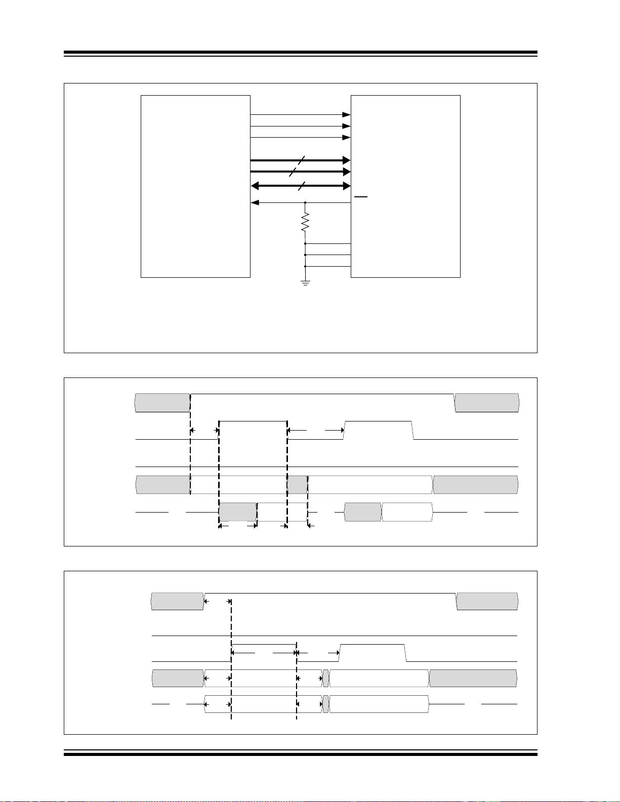
ENC424J600/624J600
Host MCU ENC624J600
CS
(1)
RD
100 k
WR
A<14:9>
(2)
A<8:0>
AD<7:0>
INT
/SPISEL
PMCSx
PMRD
PMWR
PMA<14:9>
PMA<8:0>
PMD<7:0>
INTx
(3)
6
9
8
PSPCFG2
PSPCFG3
PSPCFG4
Note 1: Use of the CS strobe from the controller is optional. If not used, tie CS to VDD.
2: Connect these pins when direct addressing of the entire SRAM buffer is required. Tie to VDD when only indirect
addressing is desired.
3: Use of the external interrupt signal to the controller is optional.
CS
RD
A<14:0>
AD<7:0> Data<7:0>Hi-Z Hi-Z
Address<14:0> Address<14:0>
Data<7:0> Hi-Z
WR
T
PSP1
T
PSP2
T
PSP4
T
PSP3
T
PSP6
CS
RD
A<14:0>
AD<7:0>
Data<7:0>Hi-Z
Address<14:0> Address<14:0>
Data<7:0> Hi-Z
WR
T
PSP8
T
PSP9
T
PSP11
T
PSP7
T
PSP10
T
PSP5
FIGURE 5-1: DEVICE CONNECTIONS FOR PSP MODE 1
FIGURE 5-2: MODE 1 READ OPERATION TIMING (TWO BYTES)
FIGURE 5-3: MODE 1 WRITE OPERATION TIMING (TWO BYTES)
DS39935C-page 54 2010 Microchip Technology Inc.

ENC424J600/624J600
Host MCU ENC624J600
CS
(1)
R/W
100 k
EN
A<14:9>
(2)
A<8:0>
AD<7:0>
INT
/SPISEL
PMCSx
PMRD/PMWR
PMENB
PMA<14:9>
PMA<8:0>
PMD<7:0>
INTx
(3)
6
9
8
PSPCFG2
PSPCFG3
PSPCFG4
+3.3V
Note 1: Use of the CS strobe from the controller is optional. If not used, tie CS to VDD.
2: Connect these pins when direct addressing of the entire SRAM buffer is required. Tie to VDD when only indirect
addressing is desired.
3: Use of the external interrupt signal to the controller is optional.
5.3.2 MODE 2
PSP Mode 2 is also an 8-bit, fully demultiplexed mode
that is available on 64-pin devices only. The parallel
interface consists of 8 bidirectional data pins (AD<7:0>)
and 9 to 15 separate address pins (A<14:0>). To select
PSP Mode 2, tie PSPCFG2 and PSPCFG3 to VSS,
while connecting PSPCFG4 to VDD. Figure 5-4
demonstrates connections required to use Mode 2.
This mode uses a combined Read/Write
an Enable (EN) strobe pin and a separate Chip Select
pin (CS). These three pins allow the host to select the
device, indicate whether a read or write operation is
desired and signal when valid data is being presented
A logic high signal on the R/W
pin indicates that a read
operation is to be performed when the EN strobe is
asserted, while a logic low indicates that a write operation is to be performed. The state of R/W
the data bus state when the EN signal is active. When
either CS, EN or R/W
is driven low, the data bus stays
in a high-impedance state.
(R/W) select,
only affects
To perform a read operation:
1. Raise the CS line (if connected to the host).
2. Raise the R/W
signal.
3. Present the address to be read onto the address
bus.
4. Raise the EN strobe.
5. Wait the required time for the access to occur.
When EN is raised high, the data bus begins to drive
out indeterminate data for a brief period, then switches
to the correct read data after the appropriate read
access time has elapsed. When the EN strobe is lowered, the data bus pins return to a high-impedance
state.
To perform a write operation:
1. Raise the CS line (if connected to the host).
2. Lower the R/W
signal.
3. Present the address onto the address bus.
4. Present the data on the data bus.
5. Strobe the EN signal high and then low.
Sample timing diagrams for reading and writing data in
this mode are provided in Figure 5-5 and Figure 5-6,
respectively.
FIGURE 5-4: DEVICE CONNECTIONS FOR PSP MODE 2
2010 Microchip Technology Inc. DS39935C-page 55

ENC424J600/624J600
CS
A<14:0>
AD<7:0>
Data<7:0>Hi-Z Hi-Z
Address<14:0> Address<14:0>
Data<7:0> Hi-Z
EN
T
PSP1
T
PSP2
T
PSP4
T
PSP3
R/W
T
PSP6
CS
A<14:0>
AD<7:0> Data<7:0>Hi-Z
Address<14:0> Address<14:0>
Data<7:0> Hi-Z
EN
T
PSP8
T
PSP9
T
PSP11
T
PSP7
T
PSP10
T
PSP5
R/W
FIGURE 5-5: MODE 2 READ OPERATION TIMING (TWO BYTES)
FIGURE 5-6: MODE 2 WRITE OPERATION TIMING (TWO BYTES)
DS39935C-page 56 2010 Microchip Technology Inc.
ENC424J600/624J600
Host MCU ENC624J600
CS
(1)
RD
100 k
WRL
A<13:8>
(3)
A<7:0>
AD<15:0>
INT
/SPISEL
PMCSx
PMRD
PMWRL
PMA<13:8>
PMA<7:0>
PMD<15:0>
INTx
(4)
6
8
16
PSPCFG2
PSPCFG3
PSPCFG4
Note 1: Use of the CS strobe from the controller is optional. If not used, tie CS to VDD.
2: WRL and WRH may optionally be tied together to form a 16-bit write strobe. See Section 5.2.3 “Write Select
Pins” for details.
3: Connect these pins when direct addressing of the entire SRAM buffer is required. Tie to VDD when only indirect
addressing is desired.
4: Use of the external interrupt signal to the controller is optional.
WRH
(2)
PMWRH
(2)
+3.3V
5.3.3 MODE 3
PSP Mode 3 is a 16-bit, fully demultiplexed mode that
is available on 64-pin devices only. The parallel interface consists of 16 bidirectional data pins (AD<15:0>)
and 8 to 14 separate address pins (A<13:0>). To select
PSP Mode 3, tie PSPCFG3 and PSPCFG4 to V
while connecting PSPCFG2 to VDD. Figure 5-7 shows
the connections required.
An active-high RD strobe and two Write strobes (WRH
and WRL) are utilized in conjunction with a separate
Chip Select (CS). These four pins allow the host to
select the device, then signal when a read operation is
desired or when valid data is being presented to be
written on either the low byte, high byte or both. For
proper operation, do not assert CS and RD while
simultaneously asserting either WRL or WRH.
In PSP Mode 3, AD<15:0> stay in a high-impedance
state any time CS or RD are low.
To perform a read operation:
1. Raise the CS line (if connected to the host).
2. Present the address to be read onto the address
bus.
3. Raise the RD strobe and wait the required time
for the access to occur.
SS,
When RD is raised high, the data bus begins driving out
indeterminate data for a brief period, then switches to
the correct read data after the appropriate read access
time has elapsed. When the RD strobe is lowered, the
data pins will return to a high-impedance state.
The device always outputs a full 16 bits of data for each
read request. If only 8 bits of data are required, read the
data from the correct pins (AD<15:8> or AD<7:0>) and
discard the remaining byte.
To perform a write operation:
1. Raise the CS line (if connected to the host).
2. Present the address onto the A<13:0> address
bus.
3. If writing to the low byte of the memory location,
present the data on AD<7:0>, and strobe the
WRL signal high and then low.
4. If writing to the high byte, present the data on the
AD<15:8> and strobe the WRH signal.
5. If writing a whole word, strobe both WRL and
WRH simultaneously.
Sample timing diagrams for reading and writing data in
this mode are provided in Figure 5-8 and Figure 5-9,
respectively.
FIGURE 5-7: DEVICE CONNECTIONS FOR PSP MODE 3
2010 Microchip Technology Inc. DS39935C-page 57
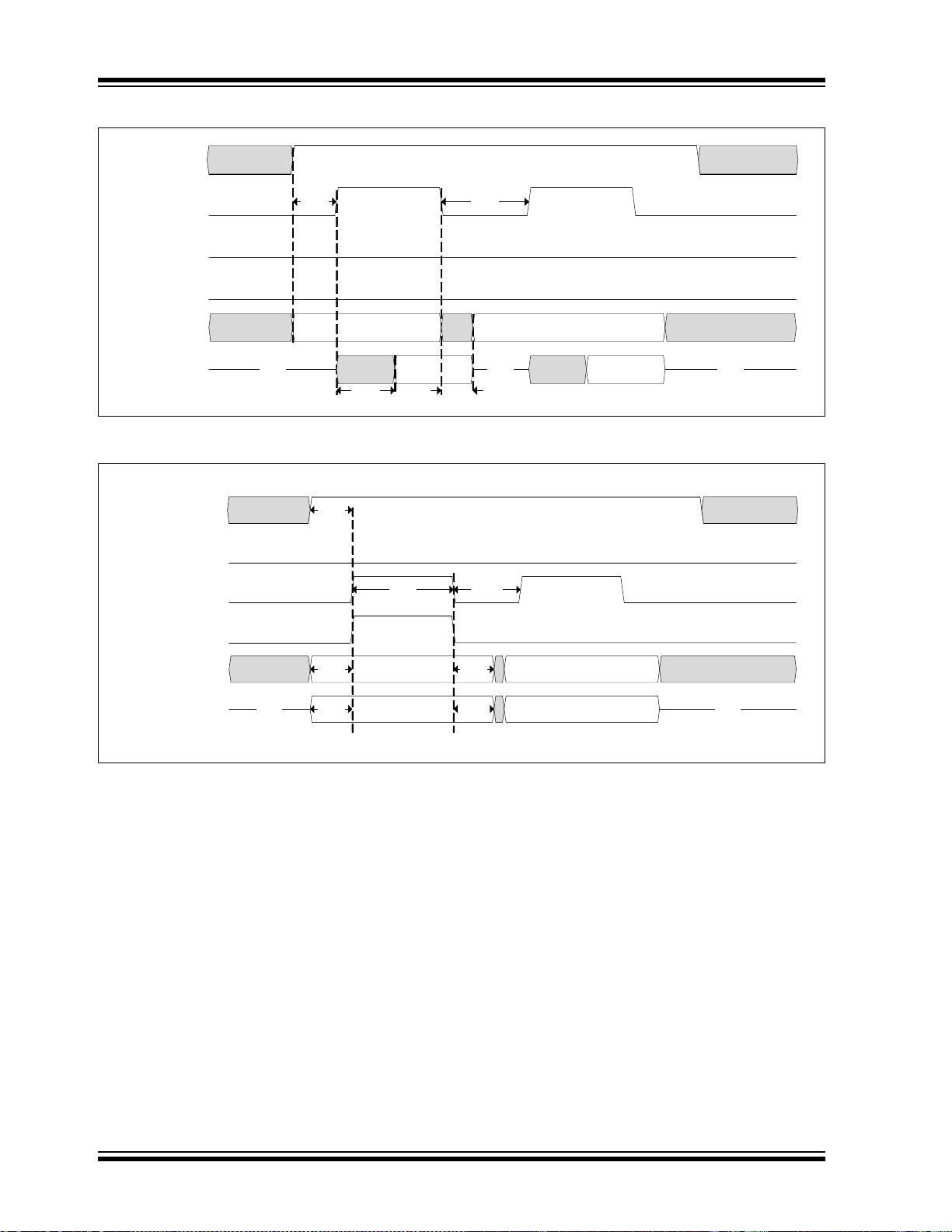
ENC424J600/624J600
CS
RD
A<13:0>
AD<15:0>
Data<15:0>Hi-Z Hi-Z
Address<13:0> Address<13:0>
Data<15:0> Hi-Z
WRH
T
PSP1
T
PSP2
T
PSP4
T
PSP3
WRL
T
PSP6
CS
RD
A<13:0>
AD<15:0>
Data<15:0>Hi-Z
Address<13:0> Address<13:0>
Data<7:0> Hi-Z
WRL
T
PSP8
T
PSP9
T
PSP11
T
PSP7
T
PSP10
T
PSP5
WRH
FIGURE 5-8: MODE 3 READ OPERATION TIMING (FOUR BYTES)
FIGURE 5-9: MODE 3 WRITE OPERATION TIMING (THREE BYTES)
DS39935C-page 58 2010 Microchip Technology Inc.

ENC424J600/624J600
Host MCU ENC624J600
CS
(1)
R/W
100 k
B0SEL
A<13:8>
(3)
A<7:0>
AD<15:0>
INT
/SPISEL
PMCSx
PMRD/PMWR
PMENB0
PMA<13:8>
PMA<7:0>
PMD<15:0>
INTx
(4)
6
8
16
PSPCFG2
PSPCFG3
PSPCFG4
B1SEL
(2)
PMENB1
(2)
+3.3V
Note 1: Use of the CS strobe from the controller is optional. If not used, tie CS to VDD.
2: B0SEL and B1SEL may optionally be tied together to form a 16-bit write strobe. See Section 5.2.3 “Write
Select Pins” for details.
3: Connect these pins when direct addressing of the entire SRAM buffer is required. Tie to VDD when only indirect
addressing is desired.
4: Use of the external interrupt signal to the controller is optional.
5.3.4 MODE 4
PSP Mode 4 is also a 16-bit, fully demultiplexed mode
that is available in 64-pin devices only. When using
PSP Mode 4, the parallel interface consists of
16 bidirectional data pins (AD<15:0>) and 8 to 14 separate address pins (A<13:0>). To select PSP Mode 4,
tie PSPCFG2 and PSPCFG4 to V
PSPCFG3 to VSS. Figure 5-10 shows the connections
required.
This mode uses a combined Read/Write (R/W
two Byte Select (B0SEL and B1SEL) lines and a separate Chip Select (CS) signal. These four pins allow the
host to select the device, indicate whether a read or
write operation is desired and signal when valid data is
being presented for writing on either the low byte, high
byte or both.
A logic-high signal on R/W
indicates that a read operation is to be performed when either the B0SEL or
B1SEL strobe is asserted, while a logic low signal
indicates that a write operation is to be performed. The
state of R/W
only affects the data bus state when either
B0SEL or B1SEL is active. When CS is driven low, R/W
is driven low, or both B0SEL and B1SEL are driven low
and the data bus stays in a high-impedance state.
To perform a read operation:
1. Raise the CS line (if connected to the host).
2. Raise the R/W
signal.
3. Present the address to be read onto the address bus.
DD, while connecting
) select,
4. Raise one or both byte select strobes.
When either BxSEL pin is raised high, the data bus
begins driving out indeterminate data for a brief period,
then switches to the correct read data after the appropriate read access time has elapsed. When B0SEL and
B1SEL are both low, the data bus pins return to a
high-impedance state.
The device always outputs a full 16 bits of data for each
read request, even if only one byte select is strobed. If
only 8 bits of data are required, read the data from the
correct pins (AD<15:8> or AD<7:0>) and discard the
remaining byte.
To perform a write operation:
1. Raise the CS line (if connected to the host).
2. Lower R/W
.
3. Present the address onto the address bus.
4. If writing to the low byte of the memory location,
present the data on the AD<7:0>; then strobe
B0SEL high, then low.
5. If writing to the high byte, present the data on
AD<15:8> and strobe B1SEL.
6. If writing a whole word, strobe both B0SEL and
B1SEL simultaneously.
Sample timing diagrams for reading and writing data in
this mode are provided in Figure 5-11 and Figure 5-12,
respectively.
FIGURE 5-10: DEVICE CONNECTIONS FOR PSP MODE 4
2010 Microchip Technology Inc. DS39935C-page 59

ENC424J600/624J600
CS
A<13:0>
AD<15:0>
Data<15:0>Hi-Z Hi-Z
Address<13:0> Address<13:0>
Data<15:0> Hi-Z
B1SEL
T
PSP2
T
PSP3
B0SEL
T
PSP1
T
PSP4
R/W
T
PSP6
CS
A<13:0>
AD<15:0>
Data<15:0>Hi-Z
Address<13:0> Address<13:0>
Data<7:0> Hi-Z
B1SEL
T
PSP9
T
PSP7
T
PSP10
T
PSP5
B0SEL
T
PSP8
T
PSP11
R/W
FIGURE 5-11: MODE 4 READ OPERATION TIMING (FOUR BYTES)
FIGURE 5-12: MODE 4 WRITE OPERATION TIMING (THREE BYTES)
DS39935C-page 60 2010 Microchip Technology Inc.

ENC424J600/624J600
5.3.5 MODE 5
PSP Mode 5 is an 8-bit, partially multiplexed mode that
is available on all devices. The parallel interface consists of 8 multiplexed address and data pins (AD<7:0>),
plus one required high address bit (AD8) and 6 optional
address-only pins (AD<14:9>).
Selecting PSP Mode 5 differs between 44-pin and
64-pin devices, as shown in Figure 5-13. For the 44-pin
ENC424J600, tie PSPCFG0 to V
ENC624J600, tie PSPCFG1 and PSPCFG2 to VSS,
and PSPCFG3 to VDD.
This mode uses active-high Read and Write (RD and
WR) strobes, as well as separate Chip Select and
Address Latch (CS and AL) lines. These four pins allow
the host to select the device, latch an address, then
indicate when a read or write operation is desired. For
proper operation, treat the RD, WR and AL strobes as
mutually exclusive whenever the ENCX24J600 is
selected. Only raise one of these to logic high at any
given time.
AD<14:8> are used as address inputs only, and are
therefore, always left in a high-impedance state. When
CS or RD is driven low, the multiplexed AD<7:0> pins
stay in a high-impedance state.
To perform a read operation:
1. Raise CS (if connected to the host).
2. Present the address to read from on AD<14:0>.
3. Strobe the AL pin high and low.
4. Set the host controller’s AD<7:0> bus pins as
inputs.
5. Raise RD.
The AD<7:0> bus begins driving out indeterminate data
for a brief period, then switches to the correct read data
after the appropriate read access time has elapsed.
When RD is lowered, the AD<7:0> pins return to a
high-impedance state.
SS. For the 64-pin
To perform a write operation:
1. Raise CS (if connected to the host).
2. Present the address to write to on AD<14:0>.
3. Strobe the AL pin.
4. Change the data on AD<7:0> from the lower
address byte to the data to be written.
5. Strobe WR high and then low.
If a subsequent read or write of the same memory
address is desired, it is possible to restrobe RD or WR
without going through another address latch cycle.
Sample timing diagrams for reading and writing data in
this mode are provided in Figure 5-14 and Figure 5-15,
respectively.
2010 Microchip Technology Inc. DS39935C-page 61
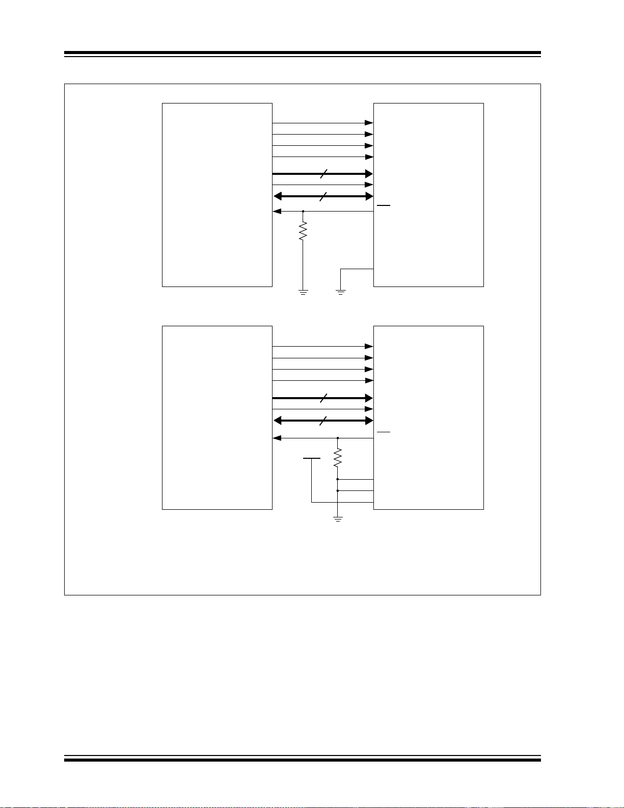
ENC424J600/624J600
Host MCU ENC424J600
CS
(1)
RD
100 k
WR
AD<14:9>
(2)
AD<7:0>
INT
/SPISEL
PMCSx
PMRD
PMWR
PMA<14:9>
PMD<7:0>
INTx
(3)
6
8
PSPCFG0
Note 1: Use of the CS strobe from the controller is optional. If not used, tie CS to VDD.
2: Connect these pins when direct addressing of the entire SRAM buffer is required. Tie to VDD when only indirect
addressing is desired.
3: Use of the external interrupt signal to the controller is optional.
Host MCU ENC624J600
100 k
INT
/SPISEL
INTx
(3)
PSPCFG1
PSPCFG2
PSPCFG3
AL
PMALL
CS
(1)
RD
WR
PMCSx
PMRD
PMWR
6
AL
PMALL
+3.3V
44-pin Devices:
64-pin Devices:
PMA8
AD8
AD<14:9>
(2)
AD<7:0>
PMA<14:9>
PMD<7:0>
8
PMA8
AD8
FIGURE 5-13: DEVICE CONNECTIONS FOR PSP MODE 5
DS39935C-page 62 2010 Microchip Technology Inc.
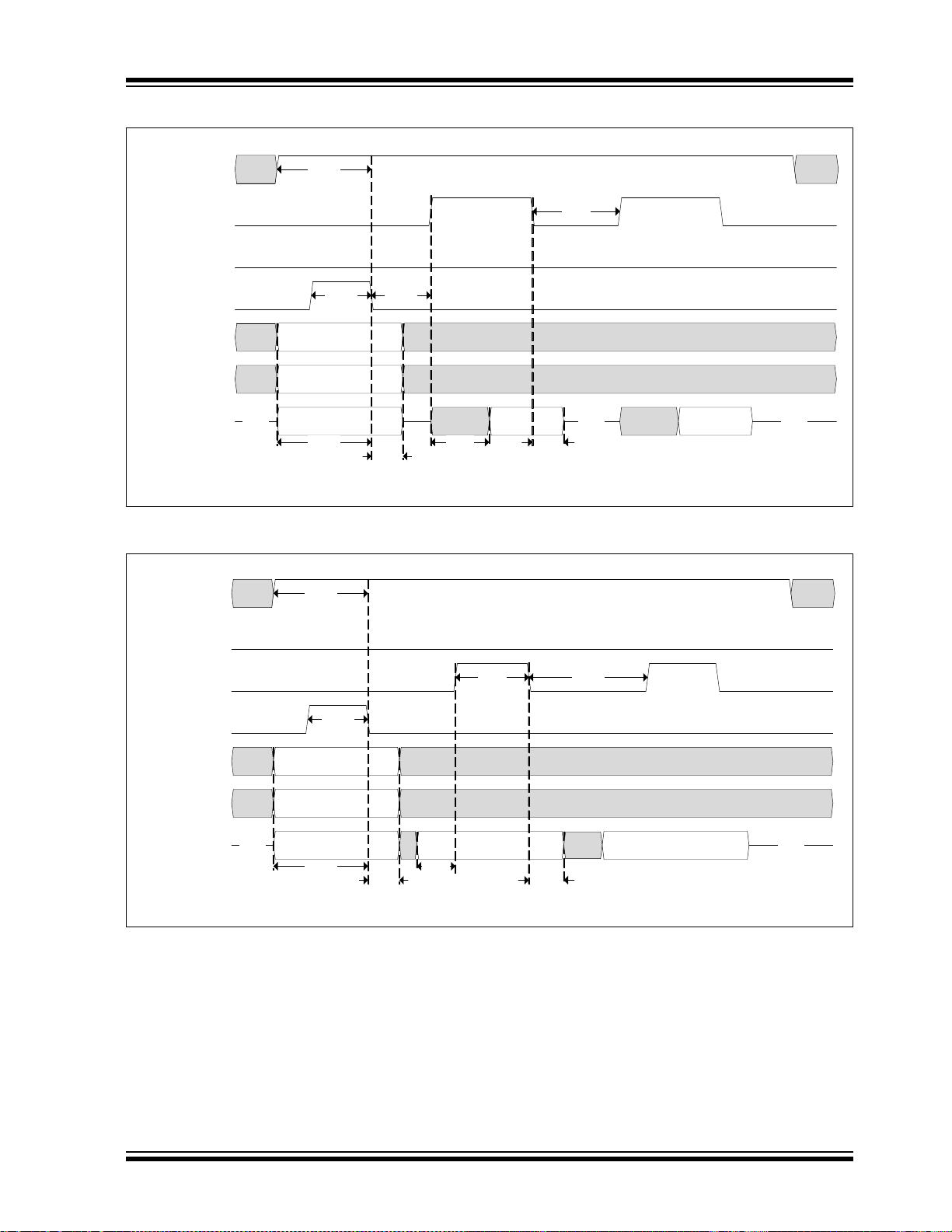
ENC424J600/624J600
CS
RD
AD<14:9>
(1)
WR
AL
Note 1: AD8 must be driven by the host controller. AD<14:9> may be tied to logic high when only indirect access is desired.
Address<14:9>
AD8
(1)
Address<8>
AD<7:0>
Data<7:0>Hi-Z Hi-Z Hi-ZAddress<7:0>
T
PSP13
T
PSP12
T
PSP12
T
PSP15
T
PSP2
T
PSP3
T
PSP4
Data<7:0>
T
PSP14
CS
RD
AD<14:9>
(1)
WR
AL
Note 1: AD8 must be driven by the host controller. AD<14:9> may be tied to logic high when only indirect access is desired.
Address<14:9>
AD8
(1)
Address<8>
AD<7:0> Data<7:0>Hi-Z Hi-ZAddress<7:0>
T
PSP13
T
PSP12
T
PSP12
T
PSP8
T
PSP10
T
PSP11
Data<7:0>
T
PSP7
T
PSP14
FIGURE 5-14: MODE 5 READ OPERATION TIMING (TWO BYTES – SAME ADDRESS)
FIGURE 5-15: MODE 5 WRITE OPERATION TIMING (TWO BYTES – SAME ADDRESS)
2010 Microchip Technology Inc. DS39935C-page 63

ENC424J600/624J600
5.3.6 MODE 6
PSP Mode 6 is also an 8-bit, partially multiplexed mode
that is available on all devices. The parallel interface
consists of 8 multiplexed address and data pins
(AD<7:0>), plus one required high address bit (AD8)
and 6 optional address-only pins (AD<14:9>).
Selecting PSP Mode 6 differs between 44-pin and
64-pin devices, as shown in Figure 5-16. For the 44-pin
ENC424J600, tie PSPCFG0 to V
ENC624J600, tie PSPCFG1 and PSPCFG3 to V
and PSPCFG2 to VSS.
This mode uses a combined Read/Write (R/W
an Enable (EN) strobe and separate Chip Select (CS)
and Address Latch (AL) lines. These four pins allow the
host to select the device, latch an address, select either
a read or write operation, then assert the Enable pin
when a read is requested or the data to be written is
valid. For proper operation, do not assert EN and AL
simultaneously while the ENCX24J600 is selected.
AD<14:8> are used as address inputs only, and are
therefore, always left in a high-impedance state. When
CS, R/W
pins stay in a high-impedance state.
or EN is driven low, the multiplexed AD<7:0>
DD. For the 64-pin
DD,
) select,
To perform a read operation:
1. Raise CS (if connected to the host).
2. Present the address to read from on AD<14:0>.
3. Strobe AL high and then low.
4. Set the host controller’s AD<7:0> bus pins as
inputs.
5. Raise R/W
6. Raise the EN strobe.
The AD<7:0> bus begins driving out indeterminate data
for a brief period, then switches to the correct read data
after the appropriate read access time has elapsed.
When EN is lowered, the multiplexed AD<7:0> pins
return to a high-impedance state.
To perform a write operation:
1. Raise CS (if connected to the host).
2. Present the address to write to on AD<14:0>.
3. Strobe AL.
4. Lower R/W
5. Change the data on AD<7:0> from the lower
address byte to the data to be written.
6. Strobe EN high, then low.
If a subsequent read or write of the same memory
address is desired, it is possible to restrobe EN without
going through another address latch cycle.
Sample timing diagrams for reading and writing data in
this mode are provided in Figure 5-17 and Figure 5-18,
respectively.
.
.
DS39935C-page 64 2010 Microchip Technology Inc.
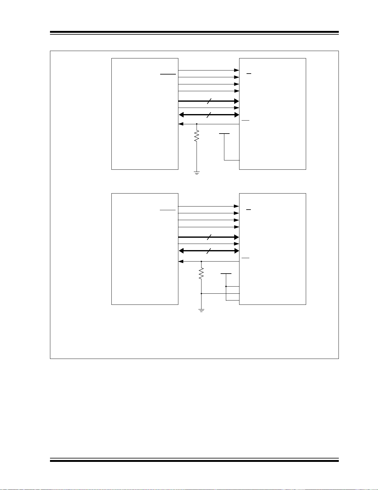
ENC424J600/624J600
Host MCU ENC424J600
CS
(1)
R/W
100 k
EN
AD<14:9>
(2)
AD<7:0>
INT
/SPISEL
PMCSx
PMRD/PMWR
PMENB
PMA<14:9>
PMD<7:0>
INTx
(3)
6
8
PSPCFG0
Note 1: Use of the CS strobe from the controller is optional. If not used, tie CS to VDD.
2: Connect these pins when direct addressing of the entire SRAM buffer is required. Tie to VDD when only indirect
addressing is desired.
3: Use of the external interrupt signal to the controller is optional.
Host MCU ENC624J600
100 k
INT
/SPISEL
INTx
(3)
PSPCFG1
PSPCFG2
PSPCFG3
AL
PMALL
6
+3.3V
44-pin Devices:
64-pin Devices:
PMA8
AD8
AD<14:9>
(2)
AD<7:0>
PMA<14:9>
PMD<7:0>
8
PMA8
AD8
+3.3V
CS
(1)
R/W
EN
PMCSx
PMRD/PMWR
PMENB
AL
PMALL
FIGURE 5-16: DEVICE CONNECTIONS FOR PSP MODE 6
2010 Microchip Technology Inc. DS39935C-page 65
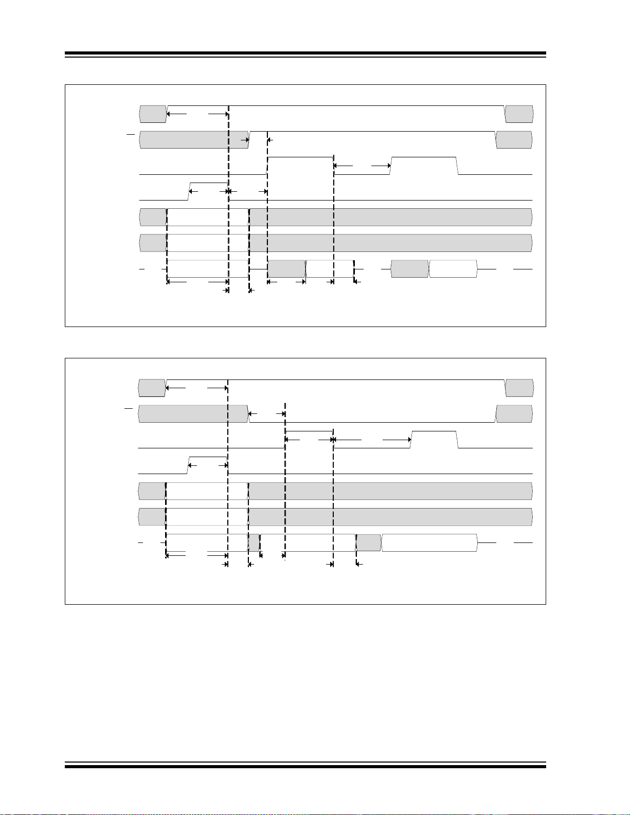
ENC424J600/624J600
CS
EN
AD<14:9>
(1)
AL
Note 1: AD8 must be driven by the host controller. AD<14:9> may be tied to logic high when only indirect access is desired .
Address<14:9>
AD8
(1)
Address<8>
AD<7:0>
Data<7:0>Hi-Z Hi-Z Hi-ZAddress<7:0>
T
PSP13
T
PSP12
T
PSP12
T
PSP15
T
PSP2
T
PSP3
T
PSP4
Data<7:0>
T
PSP1
T
PSP14
R/W
CS
AD<14:9>
(1)
EN
AL
Note 1: AD8 must be driven by the host controller. AD<14:9> may be tied to logic high when only indirect access is desired .
Address<14:9>
AD8
(1)
Address<8>
AD<7:0>
Data<7:0>Hi-Z Hi-ZAddress<7:0>
T
PSP13
T
PSP12
T
PSP12
T
PSP8
T
PSP10
T
PSP11
Data<7:0>
T
PSP7
T
PSP5
T
PSP14
R/W
FIGURE 5-17: MODE 6 READ OPERATION TIMING (TWO BYTES – SAME ADDRESS)
FIGURE 5-18: MODE 6 WRITE OPERATION TIMING (TWO BYTES – SAME ADDRESS)
DS39935C-page 66 2010 Microchip Technology Inc.

ENC424J600/624J600
Host MCU ENC624J600
100 k
AD<15:0>
INT/SPISEL
PMD<15:0>
INTx
(3)
16
PSPCFG1
PSPCFG2
PSPCFG3
CS
(1)
RD
WRL
PMCSx
PMRD
PMWRL
WRH
(2)
PMWRH
(2)
AL
PMALL
Note 1: Use of the CS strobe from the controller is optional. If not used, tie CS to VDD.
2: WRL and WRH may optionally be tied together to form a 16-bit write strobe. See Section 5.2.3 “Write Select
Pins” for details.
3: Use of the external interrupt signal to the controller is optional.
+3.3V
5.3.7 MODE 9
PSP Mode 9 is a 16-bit, fully-multiplexed mode that is
available on 64-pin devices only. The parallel interface
consists of 16 bidirectional data pins (AD<15:0>); the
lower 14 (AD<13:0>) also function as address pins. To
select PSP Mode 9, tie PSPCFG2 and PSPCFG3 to
DD, while connecting PSPCFG1 to VSS. Figure 5-19
V
shows the connections required.
This mode uses an active-high Read (RD) strobe and
two Write (WRH and WRL) strobes in conjunction with
separate Chip Select (CS) and Address Latch (AL)
inputs. These five pins allow the host to select the
device, latch an address and then signal when a read
operation is desired or when valid data is being
presented to be written to either the low byte, high byte
or both. For proper operation while the ENCX24J600 is
selected, do not assert RD or AL while simultaneously
asserting either WRL or WRH.
AD<15:0> stay in a high-impedance state any time CS
or RD is low.
To perform a read operation:
1. Raise CS (if connected to the host).
2. Present the address to read from on AD<13:0>.
3. Strobe AL high, then low.
4. Set the host controller’s AD<15:0> bus pins as
inputs.
5. Raise RD.
The AD<15:0> bus begins driving out indeterminate
data for a brief period, then switches to the correct read
data after the appropriate read access time has
elapsed. When RD is lowered, the AD<15:0> pins
return to a high-impedance state.
The device always outputs a full 16 bits of data for each
read request. If only 8 bits of data are required, read the
data from the correct pins (AD<15:8> or AD<7:0>) and
discard the remaining byte.
To perform a write operation:
1. Raise CS (if connected to the host).
2. Present the address to write to on AD<13:0>.
3. Strobe AL.
4. If writing to the low byte of the memory location,
present the data on AD<7:0>, then strobe WRL
high, then low.
5. If writing to the high byte, present the data on
AD<15:8>, then strobe WRH.
6. If writing a whole word, strobe both WRL and
WRH simultaneously.
If a subsequent read or write of the same memory
address is desired, it is possible to restrobe RD, WRL
or WRH without going through another address latch
cycle.
Sample timing diagrams for reading and writing data in
this mode are provided in Figure 5-20 and Figure 5-21,
respectively.
FIGURE 5-19: DEVICE CONNECTIONS FOR PSP MODE 9
2010 Microchip Technology Inc. DS39935C-page 67

ENC424J600/624J600
CS
RD
WRL
AL
AD<15:0> Data<15:0>Hi-Z Hi-Z Hi-ZAddress<13:0>
T
PSP13
T
PSP12
T
PSP12
T
PSP15
T
PSP2
T
PSP3
T
PSP4
Data<15:0>
WRH
T
PSP14
CS
RD
WRL
AL
AD<15:0> Data<15:0>Hi-Z Hi-ZAddress<13:0>
T
PSP13
T
PSP12
T
PSP12
T
PSP8
T
PSP10
T
PSP11
Data<7:0>
T
PSP7
WRH
T
PSP14
FIGURE 5-20: MODE 9 READ OPERATION TIMING (FOUR BYTES – SAME ADDRESS)
FIGURE 5-21: MODE 9 WRITE OPERATION TIMING (THREE BYTES – SAME ADDRESS)
DS39935C-page 68 2010 Microchip Technology Inc.
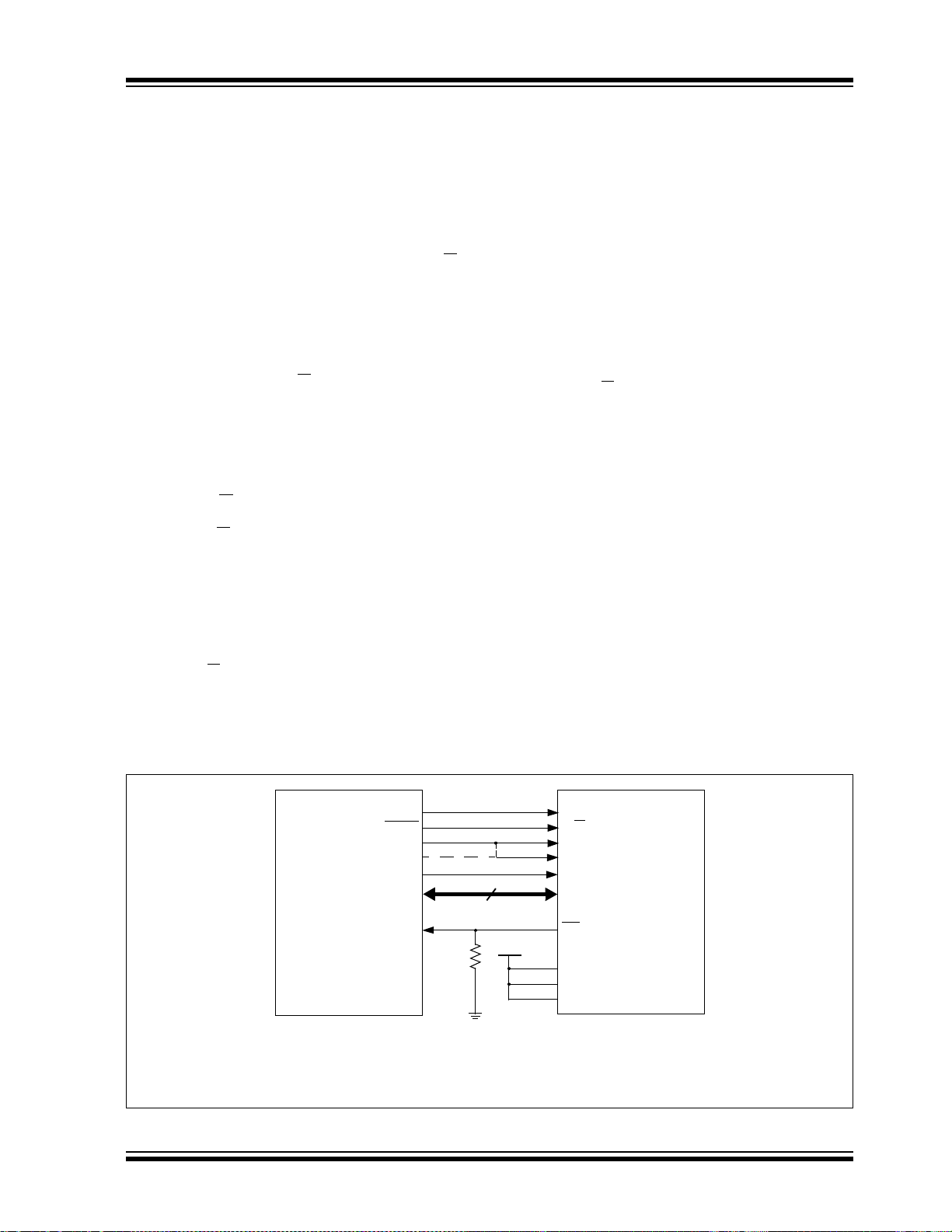
ENC424J600/624J600
Host MCU ENC624J600
AD<15:0>
PMD<15:0>
16
100 k
INT
/SPISEL
INTx
(3)
PSPCFG1
PSPCFG2
PSPCFG3
+3.3V
CS
(1)
R/W
B0SEL
PMCSx
PMRD/PMWR
PMENB0
B1SEL
(2)
PMENB1
(2)
AL
PMALL
Note 1: Use of the CS strobe from the controller is optional. If not used, tie CS to VDD.
2: B0SEL and B1SEL may optionally be tied together to form a 16-bit write strobe. See Section 5.2.3 “Write Select Pins” for
details.
3: Use of the external interrupt signal to the controller is optional.
5.3.8 MODE 10
PSP Mode 10 is also a 16-bit, fully-multiplexed mode
that is available on 64-pin devices only. The parallel
interface consists of 16 bidirectional data pins
(AD<15:0>); the lower 14 (AD<13:0>) also function as
address pins. To select PSP Mode 10, tie PSPCFG1,
PSPCFG2 and PSPCFG3 to V
the connections required.
This mode uses an active-high Read/Write (R/W
select and two Byte Select (B0SEL and B1SEL)
strobes in conjunction with separate Chip Select (CS)
and Address Latch (AL) inputs. These five pins allow
the host to select the device, latch an address, select
either a read or write operation, then assert the proper
Byte Select strobe(s) to perform the operation.
A logic high signal on the R/W
operation is to be performed when either the B0SEL or
B1SEL strobe is asserted, while a logic low signal
indicates that a write operation is to be performed. For
proper operation while the ENCX24J600 is selected,
the host controller should not assert AL while
simultaneously asserting either B0SEL or B1SEL.
The state of R/W
only affects the AD<15:0> bus state
when either B0SEL or B1SEL is active. When CS is
driven low, R/W
is driven low, or both B0SEL and
B1SEL are driven low, AD<15:0> stays in a
high-impedance state.
To perform a read operation:
1. Raise CS (if connected to the host).
2. Present the address to be read onto AD<13:0>.
3. Strobe AL high, then low.
4. Raise R/W
.
5. Set the host controller’s AD<15:0> bus pins as
inputs.
6. Raise either B0SEL or B1SEL, or both.
DD. Figure 5-22 shows
pin indicates that a read
When either BxSEL pin is raised high, the AD<15:0>
bus begins driving out indeterminate data for a brief
period, then switches to the correct read data after the
appropriate read access time has elapsed. When
B0SEL and B1SEL are both low, AD<15:0> return to a
high-impedance state.
The device always outputs a full 16 bits of data for each
read request, even if only one byte select is strobed. If
)
only 8 bits of data are required, read the data from the
correct pins (AD<15:8> or AD<7:0>) and discard the
remaining byte.
To perform a write operation:
1. Raise CS (if connected to the host).
2. Present the address to write to on AD<13:0>.
3. Strobe AL.
4. Lower R/W
.
5. If writing to the low byte of the memory location,
present the data on AD<7:0>, then strobe
B0SEL.
6. If writing to the high byte, present the data on
AD<15:8>, then strobe the B1SEL signal.
7. If writing a whole word, strobe both B0SEL and
B1SEL simultaneously.
If a subsequent read or write of the same memory
address is desired, it is possible to restrobe B0SEL or
B1SEL without going through another address latch
cycle.
Sample timing diagrams for reading and writing data in
this mode are provided in Figure 5-23 and Figure 5-24,
respectively.
FIGURE 5-22: DEVICE CONNECTIONS FOR PSP MODE 1
2010 Microchip Technology Inc. DS39935C-page 69

ENC424J600/624J600
CS
B0SEL
AL
AD<15:0> Data<15:0>Hi-Z Hi-Z Hi-ZAddress<13:0>
T
PSP13
T
PSP12
T
PSP12
T
PSP15
T
PSP2
T
PSP3
T
PSP4
Data<15:0>
B1SEL
T
PSP1
T
PSP14
R/W
CS
B0SEL
AL
AD<15:0> Data<15:0>Hi-Z Hi-ZAddress<13:0>
T
PSP13
T
PSP12
T
PSP8
T
PSP10
T
PSP11
Data<7:0>
B1SEL
T
PSP5
T
PSP14
R/W
T
PSP12
T
PSP7
FIGURE 5-23: MODE 10 READ OPERATION TIMING (FOUR BYTES – SAME ADDRESS)
FIGURE 5-24: MODE 10 WRITE OPERATION TIMING (THREE BYTES – SAME ADDRESS)
DS39935C-page 70 2010 Microchip Technology Inc.

ENC424J600/624J600
SA
Padding
FCS
(1)
Number Field Comments
6
46-1500
4
DA
Destination Address,
such as Multicast, Broadcast or Unicast
Source Address
Packet Payload
Frame Check Sequence – CRC
Type/Length
Data
of Bytes
6
2
Type of Packet or the Length of the Packet
(with optional padding)
7
Filtered Out by the Module
SFD
1
Start-Of-Frame Delimiter
(filtered out by the module)
Used in the
Calculation
of the FCS
Note 1: The FCS is transmitted starting with bit 31 and ending with bit 0.
Preamble
Start of Stream/
6.0 ETHERNET OVERVIEW
Before discussing the use of ENC424J600/624J600
devices in Ethernet applications, it may be helpful to
review the structure of a typical data frame. For more
detailed information, refer to IEEE 802.3 Standard, which
defines the Ethernet protocol, or to Microchip Application
Note AN1120, “Ethernet Theory of Operation”.
6.1 Frame Format
Ethernet communications utilize a series of frames to
transmit data between nodes. (These frames are also
commonly referred to as “packets”, and in the context of
this document, the two terms will be used interchangeably.) Compliant Ethernet frames are between 64 and
1518 bytes long. They consist of five or six different
fields: a destination MAC address, source MAC
address, type/length field, data payload, optional
padding field and a Cyclic Redundancy Check (CRC).
Additionally, when transmitted on the Ethernet medium,
a start of stream/preamble field and a Start-Of-Frame
(SOF) delimiter byte are appended to the beginning of
the Ethernet frame. Thus, traffic seen on the twisted-pair
cabling will appear as shown in Figure 6-1.
FIGURE 6-1: ETHERNET PACKET FORMAT
6.1.1 START OF STREAM/PREAMBLE
AND START-OF-FRAME DELIMITER
When using ENC424J600/624J600 devices, the start
of stream/preamble and Start-Of-Frame delimiter fields
are automatically generated for transmitted frames and
stripped from received ones. These bytes are not
written to the data buffer and the host controller does
not need to account for these bytes.
6.1.2 DESTINATION ADDRESS
The destination address is a 6-byte field containing the
MAC address of the device to which the frame is
directed. If the Least Significant bit in the first byte of
this address is clear (i.e., the first byte of the address is
even), the address is a Unicast address. For example,
00-00-BA-BE-F0-0D and 32-45-DE-AD-BE-EF Unicast
addresses, while 01-00-BA-BE-F0-0D and
33-45-DE-AD-BE-EF are not. Frames with a Unicast
destination are designated for usage by the addressed
node only.
2010 Microchip Technology Inc. DS39935C-page 71

ENC424J600/624J600
If the Least Significant bit in the first byte of this address
is set (i.e., the byte is odd), the address is a Multicast
destination. From the previous example,
01-00-BA-BE-F0-0D and 33-45-DE-AD-BE-EF are
Multicast addresses. Multicast frames are designated
for use by a selected group of Ethernet nodes. The
Multicast address, FF-FF-FF-FF-FF-FF, is reserved; it
is known as the Broadcast address and is directed to all
nodes on the network.
ENC424J600/624J600 devices incorporate several
packet filters which can be configured to accept or discard Unicast, Multicast and/or Broadcast frames. For
details about these and other receive filters, refer to
Section 10.0 “Receive Filters”. When transmitting
frames, the host controller is responsible for writing the
desired destination address into the transmit buffer.
6.1.3 SOURCE ADDRESS
The source address is a 6-byte field containing the
MAC address of the node which transmitted the Ethernet frame. Every Ethernet device must have a globally
unique MAC address. Each ENC424J600/624J600
device has a unique address which is loaded into the
MAADR registers on power-up. This value can be used
as is, or the registers may be reconfigured with a
different address.
6.1.4 TYPE/LENGTH
The type/length field is a 2-byte field indicating the protocol to which the frame belongs. Applications using
standards such as Internet Protocol (IP) or Address
Resolution Protocol (ARP) should use the type code
specified in the appropriate standards document.
Alternately, this field can be used as a length field when
implementing proprietary networks. Typically, any
value of 1500 (05DCh) or smaller is considered to be a
length field and specifies the amount of non-padding
data which follows in the data field.
6.1.5 DATA
The data field typically consists of between 0 and
1500 bytes of payload data for each frame.
ENC424J600/624J600 devices are capable of transmitting and receiving frames larger than this when the
Huge Frame Enable bit, HFRMEN (MACON2<2>), is
set. However, these larger data frames violate Ethernet
specifications and will likely be dropped by most
Ethernet nodes.
6.1.6 PADDING
The padding field is a variable length field appended to
meet IEEE 802.3 specification requirements when
transmitting small data payloads. As mentioned, the
minimum Ethernet frame size is 64 bytes. Removing
the 18 bytes of address and type information, and the
terminating 4-byte CRC, leaves a minimum of 46 bytes.
Smaller frames must be padded to fill this space.
When transmitting frames, ENC424J600/624J600
devices can automatically generate zero padding if the
PADCFG<2:0> bits (MACON2<7:5>) are configured to
do so. Otherwise, the application must append the
appropriate padding. The device will not prevent the
transmission of these “runt” frames if the host
commands such an action, but the frame is likely to be
dropped by other nodes.
When receiving frames, ENC424J600/624J600 devices
accept and write all padding to the receive buffer.
Frames shorter than the required 64 bytes can optionally
be filtered by the Runt Error Reject filter, described in
Section 10.4 “Runt Error Rejection Filter”.
6.1.7 CRC
The CRC is a 4-byte field containing a standard 32-bit
CRC calculated over the destination, source, type, data
and padding fields. It allows for the detection of
transmission errors.
When transmitting frames, ENC424J600/624J600
devices can automatically generate and append a valid
CRC if the PADCFG<2:0> bits are configured to do so.
Otherwise, the host controller must generate and
append this value. It is strongly recommended that the
PADCFG bits be configured so that the hardware
automatically manages this field.
When receiving frames, ENC424J600/624J600
devices accept and write the CRC field to the receive
buffer. Frames with invalid CRC values can be
discarded by the CRC Error Rejection filter, described
Section 10.3 “CRC Error Rejection Filter”.
in
DS39935C-page 72 2010 Microchip Technology Inc.
ENC424J600/624J600
POR
Reset SFRs and
Reset TX
Reset RX
Transmit Reset
Receive Reset
System Reset
(ETHRST)
Reset I/O Interface
and CLKOUT
Reset PHY
PHY Reset
(TXRST)
(RXRST)
(PRST)
SPI Bank Select
7.0 RESET
ENC424J600/624J600 differentiates between five
types of Resets:
• Power-on Reset (POR)
• System Reset
• Transmit Only Reset
• Receive Only Reset
• PHY Subsystem Reset
A simplified block diagram of the on-chip Reset circuit
is shown in Figure 7-1.
7.1 Power-on Reset
Power-on Reset occurs when VDD rises above VPOR.
This allows the device to start in the initialized state
when VDD is adequate for the device’s digital logic to
operate correctly. The POR circuitry is always enabled.
To ensure proper POR operation, the application circuit
must meet the specified minimum rise rate of VDD
(SVDD, DC parameter D003).
After a Power-on Reset, the contents of the SRAM buffer
and cryptographic memories are unknown. However, all
registers will be loaded with their specified Reset values.
The PHY and other logic should still not be accessed
immediately after the POR. See
for the recommended Reset procedure.
Section 8.1 “Reset”
7.2 System Reset
A System Reset reverts all registers back to their
default Reset values, with the exception of
COCON<3:0> (ECON2<11:8>), which controls the
frequency output on CLKOUT. All transmit, receive,
MAC, PHY, DMA and cryptographic logic are reset.
Additionally, if the SPI interface is used, the current
internal bank selection is reset to Bank 0. The packet
buffer, cryptographic memories and the PSP address
latch used in Multiplexed Parallel modes are unaffected
by a System Reset.
To initiate a System Reset, set the ETHRST bit
(ECON2<4>). The bit is automatically cleared by
hardware. After setting ETHRST, a delay of 25
required before the ENCX24J600 can be accessed
again through the SPI or PSP interfaces. Additionally,
all PHY registers and status bits derived from the PHY
should not be accessed or used for an additional period
of 256 s.
A System Reset does not cause the SPISEL and
PSPCFGx pin states to be relatched. Therefore, the currently selected controller interface remains available
after issuing a System Reset and waiting the required
25 s.
s is
FIGURE 7-1: ON-CHIP RESET CIRCUIT
2010 Microchip Technology Inc. DS39935C-page 73

ENC424J600/624J600
7.3 Transmit Only Reset
A Transmit Only Reset is performed by setting the
TXRST bit (ECON2<6>). The transmit logic is held in
Reset until the bit is cleared. Any pending transmission
is aborted and TXRTS (ECON1<1>) is cleared. To
resume normal operation, clear the TXRST bit.
Both the POR and System Resets automatically perform
a Transmit Reset, so this step does not need to be performed after a System or Power-on Reset. Only the
transmit logic is affected by this operation. Other register
and control blocks are not affected by this event.
7.4 Receive Only Reset
A Receive Only Reset is performed by setting the
RXRST bit (ECON2<5>). The receive logic is held in
Reset until the bit is cleared. Any packet being received
is aborted and RXEN (ECON1<0>) is cleared. To
resume normal operation, clear the RXRST bit.
Both the POR and System Resets automatically perform
a Receive Reset, so this step does not need to be performed after a System or Power-on Reset. Only the
receive logic is affected by this operation. Other register
and control blocks are not affected by this event.
Following a Receive Only Reset, it is necessary to
manually reconfigure the RX SFRs for normal receive
operation again. For example, applications must clear
the PKTCNT field in ESTAT by setting the PKTDEC bit
(ECON1<8>) enough times for the count to reach zero.
Similarly, applications must reset the ERXST and
ERXTAIL Pointers before enabling reception again with
the RXEN bit.
7.5 PHY Subsystem Reset
The PHY module may be reset by setting the PRST bit
(PHCON1<15>). The PHY register contents all revert
to their default values.
Unlike the Transmit and Receive Only Resets, the PHY
cannot be removed from Reset immediately after setting
PRST. The PHY requires a delay, after which the
hardware automatically clears the PRST bit. It is recommended that, after issuing a Reset, the host controller
polls PRST and waits for it to be cleared by hardware
before using the PHY.
The POR and System Resets automatically perform a
PHY Reset, so this step does not need to be performed
after a System or Power-on Reset. Only the PHY is
affected by this operation. Other register and control
blocks are not affected by this event.
DS39935C-page 74 2010 Microchip Technology Inc.

ENC424J600/624J600
8.0 INITIALIZATION
Before using an ENCX24J600 device to transmit and
receive packets, certain device settings must be initialized. Depending on the application, some configuration
options may be left set to their default values. Those
that need to be changed are typically set once after
power-up and not changed thereafter.
8.1 Reset
Because it is possible for the host controller to reset
independently from the ENCX24J600 (for example,
when using an external debugger to reprogram the
host), it is recommended that software issue a System
Reset of the ENCX24J600 as the first step of its
ordinary initialization routine.
Also, since it is possible for the host controller to exit its
POR, begin code execution before the ENCX24J600
exits POR and latches the Interface mode, special care
should be taken in the software to ensure that it does
not attempt to blindly initialize the ENCX24J600
registers before the device is actually out of Reset. To
take care of these potential pitfalls, it is recommended
that firmware take a write-verify-reset-reverify
approach to ensure proper start-up. For example:
1. Write 1234h to EUDAST.
2. Read EUDAST to see if it now equals 1234h. If
it does not, the SPI/PSP interface may not be
ready yet, so return to step 1 and try again.
3. Poll CLKRDY (ESTAT<12>) and wait for it to
become set.
4. Issue a System Reset command by setting
ETHRST (ECON2<4>).
5. In software, wait at least 25
take place and the SPI/PSP interface to begin
operating again.
6. Read EUDAST to confirm that the System Reset
took place. EUDAST should have reverted back
to its Reset default of 0000h.
7. Wait at least 256
PHY status bits to become available.
The ENCX24J600 is now ready to accept further
commands.
s for the PHY registers and
8.2 CLKOUT Frequency
If the ENCX24J600 is providing a system clock for the
host controller, or other hardware features of the
application, it is recommended that the application configure the output frequency on the CLKOUT pin first.
The frequency is set by using the COCON<3:0> bits
(ECON2<11:8>). By default, the output frequency on
CLKOUT after a POR is 4 MHz. The last programmed
frequency is maintained after all other Reset events.
For more information on using the output of the
CLKOUT pin, see
Section 2.2 “CLKOUT Pin”.
s for the Reset to
8.3 Receive Buffer
Before packet reception is enabled, the receive buffer
must be configured by programming the ERXST
Pointer. All memory between this pointer and the end of
the physical memory (5FFFh), including those
addresses, are reserved as the receive buffer for
incoming packets. The value of ERXST must be
word-aligned, since all incoming frames must be stored
beginning at even addresses.
If an application expects a large amount of incoming
traffic or frequent packet delivery, it is recommended
that it allocate a larger receive buffer. Applications
needing more space for saving old packets or other
temporary storage, or wishing to hold several packets
ready for transmission, can allocate less memory for
the receive buffer.
Reception of incoming packets begins at the address
designated by ERXST.
8.4 Transmit Buffer
No specific transmit buffer is defined. The host applications may write frames to be transmitted to any unused
space in the SRAM buffer; no initialization is necessary.
8.5 Receive Filters
Before enabling packet reception, configure the receive
filters to eliminate unwanted incoming packets. See
Section 10.0 “Receive Filters” for details.
8.6 MAC Initialization
Once the receive buffer and filters are properly
configured, several MAC registers must be configured.
The order of programming is unimportant.
• If flow control operation is desired, configure the
flow control module as described in Section 11.0
“Flow Control”.
• Verify that the TXCRCEN (MACON2<4>) and
PADCFG<2:0> (MACON2<7:5>) bits are set
correctly. Most applications will not need to modify
these settings from their power-on defaults.
• Program the MAMXFL register with the maximum
frame length to be accepted (received or transmitted). Most network nodes are configured to
handle packets that are 1518 bytes or less
(1522 bytes or less if VLAN tagging is used).
Alternately, set HFRMEN (MACON2<2>) to
accept any size frame.
• Set the RXEN bit (ECON1<0>) to enable packet
reception by the MAC.
2010 Microchip Technology Inc. DS39935C-page 75

ENC424J600/624J600
8.6.1 PREPROGRAMMED MAC ADDRESS
As shipped, each ENCX24J600 device has been
preprogrammed with a unique MAC address. This
value is stored in nonvolatile memory and reloaded into
the MAADR registers after every Power-on and System
Reset. The factory preprogrammed MAC address is
permanent and will be restored to the MAC registers
after each Reset.
The preprogrammed address in nonvolatile memory
cannot be changed by the user, but it can be overwritten in the SFRs. If the user requires a different MAC
address value, the MAADR registers will need to be
written with the new MAC values by the host
application after each Reset.
8.7 PHY Initialization
Depending on the application, the PHY may need to be
configured during initialization. Typically, when using
auto-negotiation, users should write 0x05E1 to PHANA
to advertise flow control capability. Only special test
code, such as when attempting to do loopback tests,
needs other settings in the PHY to be reconfigured.
8.8 Other Considerations Following Reset
Beyond the steps already described, there are additional configuration options that may need to be
adjusted following a device Reset. Normally, the default
configurations of these items on Power-on Reset do
not need to be changed.
For Half-Duplex mode:
• Verify that DEFER (MACON2<14>), BPEN
(MACON2<13>) and NOBKOFF (MACON2<12>)
are set correctly. These bits only apply when
operating in Half-Duplex mode; most applications
do not need to modify these settings from their
power-on defaults. For IEEE 802.3 compliance,
keep the DEFER bit set.
• Configure the Non-Back-to-Back Inter-Packet
Gap register, MAIPG (Register 8-5). Most applications program this register to 12h, which selects
maximum performance while complying with the
IEEE 802.3 IPG previously specified.
• Set the MAXRET<3:0> (MACLCON<3:0>) bits to
select the maximum number of retransmission
attempts after a collision is detected. Most
applications do not need to change this from the
default value.
For Full-Duplex mode:
• Configure the low byte of the Non-Back-to-Back
Inter-Packet Gap register, MAIPGL. Most applications program this register to 12h, which selects
maximum performance while complying with the
IEEE 802.3 IPG previously specified.
8.9 After Link Establishment
Several MAC configuration parameters are dependent
upon the current duplex mode of the link. Once
auto-negotiation completes, or the speed and duplex
modes are manually reconfigured, these registers must
be updated accordingly. For details about
auto-negotiation and manual speed/duplex
configuration, refer to Section 12.0 “Speed/Duplex
Configuration and Auto-Negotiation”.
Once these steps are performed, packet reception is
re-enabled by setting RXEN (ECON1<0>). The host
controller may also begin to transmit packets as
described in Section 9.1 “Transmitting Packets”.
Before transmitting the first packet after link establishment or auto-negotiation, the MAC duplex configuration
must be manually set to match the duplex configuration
of the PHY. To do this, configure FULDPX
(MACON2<0>) to match PHYDPX (ESTAT<10>).
For Half-Duplex mode, configure the Back-to-Back
Inter-Packet Gap register, MABBIPG (Register 8-4), to
set the nibble time offset delay between the end of one
transmission and the beginning of the next in a
back-to-back sequence. Program the register value as
the desired period in nibble times, minus 6. Most
applications will program this register to 12h, which
represents the minimum Inter-Packet Gap (IPG)
specified by IEEE 802.3, of 0.96
9.6 s (at 10 Mb/s).
For Full-Duplex mode, configure the Back-to-Back
Inter-Packet Gap register, MABBIPG, to set the nibble
time offset delay between the end of one transmission
and the beginning of the next in a back-to-back
sequence. The register value should be programmed
as the desired period in nibble times, minus 3. Most
applications will program this register to 15h, which
represents the minimum IEEE 802.3 specified
Inter-Packet Gap (IPG) of 0.96
9.6 s (at 10 Mb/s).
s (at 100 Mb/s) or
s (at 100 Mb/s) or
DS39935C-page 76 2010 Microchip Technology Inc.

ENC424J600/624J600
REGISTER 8-1: ECON2: ETHERNET CONTROL REGISTER 2
R/W-1 R/W-1 R/W-0 R/W-0 R/W-1
(1)
ETHEN STRCH TXMAC SHA1MD5 COCON3 COCON2 COCON1 COCON0
bit 15 bit 8
R/W-0 R/W-0 R/W-0 R/W-0 R/W-0 R/W-0 R/W-0 R/W-0
AUTOFC TXRST RXRST ETHRST MODLEN1 MODLEN0 AESLEN1 AESLEN0
bit 7 bit 0
Legend:
R = Readable bit W = Writable bit U = Unimplemented bit, read as ‘0’
-n = Value at POR ‘1’ = Bit is set ‘0’ = Bit is cleared x = Bit is unknown
bit 15 ETHEN: Ethernet Enable bit
1 = Device is enabled (normal operation)
0 = Device is disabled (reduced power)
bit 14 STRCH: LED Stretching Enable bit
1 = Stretch transmit, receive and collision events on LEDA and LEDB to 50 ms
0 = LEDA and LEDB outputs show real-time status without stretching
bit 13 TXMAC: Automatically Transmit MAC Address Enable bit
1 = MAADR1-MAADR6 registers are automatically inserted into the source address field of all
transmitted packets
0 = No automatic source address insertion
bit 12 SHA1MD5: SHA-1/MD5 Hash Control bit
1 = Hashing engine computes a SHA-1 hash
0 = Hashing engine computes an MD5 hash
bit 11-8 COCON<3:0>: CLKOUT Frequency Control bits
(1)
1111 = 50 kHz nominal ((4 * FOSC)/ 2000)
1110 = 100 kHz nominal ((4 * FOSC)/ 1000)
1101 = No output (DC sinking to VSS)
1100 = 3.125 MHz nominal ((4 * FOSC)/32)
1011 = 4.000 MHz nominal ((4 * FOSC)/25)
1010 = 5.000 MHz nominal ((4 * FOSC)/20)
1001 = 6.250 MHz nominal ((4 * FOSC)/16)
1000 = 8.000 MHz nominal ((4 * FOSC)/12.5); duty cycle is not 50%
0111 = 8.333 MHz nominal ((4 * FOSC)/12)
0110 = 10.00 MHz nominal ((4 * FOSC)/10)
0101 = 12.50 MHz nominal ((4 * FOSC)/8)
0100 = 16.67 MHz nominal ((4 * FOSC)/6)
0011 = 20.00 MHz nominal ((4 * FOSC)/5)
0010 = 25.00 MHz nominal ((4 * FOSC)/4)
0001 = 33.33 MHz nominal ((4 * FOSC)/3)
0000 = No output (DC sinking to VSS)
bit 7 AUTOFC: Automatic Flow Control Enable bit
1 = Automatic flow control is enabled
0 = Automatic flow control is disabled
bit 6 TXRST: Transmit Logic Reset bit
1 = Transmit logic is held in Reset. TXRTS (ECON1<1>) is automatically cleared by hardware when
this bit is set.
0 = Transmit logic is not in Reset (normal operation)
R/W-0
(1)
R/W-1
(1)
R/W-1
(1)
Note 1: Reset value on POR events only. All other Resets leave these bits unchanged.
2010 Microchip Technology Inc. DS39935C-page 77

ENC424J600/624J600
REGISTER 8-1: ECON2: ETHERNET CONTROL REGISTER 2 (CONTINUED)
bit 6 RXRST: Receive Logic Reset bit
1 = Receive logic is held in Reset. RXEN (ECON1<0>) is automatically cleared by hardware when this
bit is set.
0 = Receive logic is not in Reset (normal operation)
bit 4 ETHRST: Master Ethernet Reset bit
1 = All TX, RX, MAC, PHY, DMA, modular exponentiation, hashing and AES logic, and registers
(excluding COCON) are reset. Hardware self-clears this bit to ‘0’. After setting this bit, wait at least
25 s before attempting to read or write to the ENCX24J600 via the SPI or PSP interface.
0 = Device is not in Reset (normal operation)
bit 3-2 MODLEN<1:0>: Modular Exponentiation Length Control bits
11 = Reserved
10 = 1024-bit modulus and operands
01 = 768-bit modulus and operands
00 = 512-bit modulus and operands
bit 1-0 AESLEN<1:0>: AES Key Length Control bits
11 = Reserved
10 = 256-bit key
01 = 192-bit key
00 = 128-bit key
Note 1: Reset value on POR events only. All other Resets leave these bits unchanged.
DS39935C-page 78 2010 Microchip Technology Inc.

ENC424J600/624J600
REGISTER 8-2: EIDLED: ETHERNET ID STATUS/LED CONTROL REGISTER
R/W-0 R/W-0 R/W-1 R/W-0 R/W-0 R/W-1 R/W-1 R/W-0
LACFG3 LACFG2 LACFG1 LACFG0 LBCFG3 LBCFG2 LBCFG1 LBCFG0
bit 15 bit 8
R-0R-0R-1RRRRR
DEVID2 DEVID1 DEVID0 REVID4 REVID3 REVID2 REVID1 REVID0
bit 7 bit 0
Legend:
R = Readable bit W = Writable bit U = Unimplemented bit, read as ‘0’
-n = Value at POR ‘1’ = Bit is set ‘0’ = Bit is cleared x = Bit is unknown
bit 15-12,
bit 11-8
bit 7-5 DEVID<2:0>: Device ID bits
bit 4-0 REVID<4:0>: Silicon Revision ID bits
LACFG<3:0>: LEDA Configuration bits and
LBCFG<3:0: LEDB Configuration bits
1111 = Display link and speed state, transmit and receive events
1110 = Display link and duplex state, transmit and receive events
1101 = Reserved
1100 = Display link state, collision events; pin is driven high when a link is present and driven low
temporarily when a collision occurs
1011 = Display link state, transmit and receive events; pin is driven high when a link is present and
driven low while a packet is being received or transmitted
1010 = Display link state, receive events; pin is driven high when a link is present and driven low while
a packet is being received
1001 = Display link state, transmit events; pin is driven high when a link is present and driven low while
a packet is being transmitted
1000 = Display speed state; pin is driven high when in 100 Mbps mode and a link is present
0111 = Display duplex state; pin is driven high when the PHY is in full duplex (PHYDPX (ESTAT<10>)
is ‘1’) and a link is present
0110 = Display transmit and receive events; pin is driven high while a packet is either being received
or transmitted
0101 = Display receive events; pin is driven high while a packet is being received
0100 = Display transmit events; pin is driven high while a packet is being transmitted
0011 = Display collision events; pin is temporarily driven high when a collision occurs
0010 = Display link state; pin is driven high when linked
0001 = On (pin is driven high)
0000 = Off (pin is driven low)
001 = ENC624J600 family device
Indicates current silicon revision.
(1)
(1)
Note 1: These configurations require that a bi-color LED be connected between the LEDA and LEDB pins, and
that LACFG<3:0> and LBCFG<3:0> be set to the same value. See Section 2.5.1 “Using Bi-Color
LEDs” for detailed information.
2010 Microchip Technology Inc. DS39935C-page 79

ENC424J600/624J600
REGISTER 8-3: MACON2: MAC CONTROL REGISTER 2
U-0 R/W-1 R/W-0 R/W-0 U-0 U-0 R/W-0 R/W-0
— DEFER BPEN NOBKOFF — — r r
bit 15 bit 8
R/W-1 R/W-0 R/W-1 R/W-1 R/W-0 R/W-0 R/W-1 R/W-0
PADCFG2 PADCFG1 PADCFG0 TXCRCEN PHDREN HFRMEN
bit 7 bit 0
Legend:
R = Readable bit W = Writable bit U = Unimplemented bit, read as ‘0’
-n = Value at POR ‘1’ = Bit is set ‘0’ = Bit is cleared x = Bit is unknown
bit 15 Unimplemented: Read as ‘0’
bit 14 DEFER: Defer Transmission Enable bit (applies to half duplex only)
1 = When the medium is occupied, the MAC will wait indefinitely for it to become free when attempting
to transmit (use this setting for IEEE 802.3 compliance)
0 = When the medium is occupied, the MAC will abort the transmission after the excessive deferral
limit is reached (24,288 bit times)
bit 13 BPEN: No Backoff During Back Pressure Enable bit (applies to half duplex only)
1 = After incidentally causing a collision during back pressure, the MAC immediately begins retransmitting
0 = After incidentally causing a collision during backpressure, the MAC delays using the binary
exponential backoff algorithm before attempting to retransmit (normal operation)
bit 12 NOBKOFF: No Backoff Enable bit (applies to half duplex only)
1 = After any collision, the MAC immediately begins retransmitting
0 = After any collision, the MAC delays using the binary exponential backoff algorithm before
attempting to retransmit (normal operation)
bit 11-10 Unimplemented: Read as ‘0’
bit 9-8 Reserved: Write as ‘0’
bit 7-5 PADCFG<2:0>: Automatic Pad and CRC Configuration bits
111 = All short frames are zero-padded to 64 bytes and a valid CRC is then appended
110 = No automatic padding of short frames
101 = MAC automatically detects VLAN protocol frames which have a 8100h type field and auto-
matically pad to 64 bytes. If the frame is not a VLAN frame, it will be padded to 60 bytes. After
padding, a valid CRC is appended.
100 = No automatic padding of short frames
011 = All short frames are zero-padded to 64 bytes and a valid CRC is then appended
010 = No automatic padding of short frames
001 = All short frames will be zero-padded to 60 bytes and a valid CRC is then appended
000 = No automatic padding of short frames
bit 4 TXCRCEN: Transmit CRC Enable bit
1 = MAC appends a valid CRC to all frames transmitted regardless of the PADCFG bits. TXCRCEN
must be set if the PADCFG bits specify that a valid CRC will be appended.
0 = MAC does not append a CRC. The last 4 bytes are checked and if it is an invalid CRC, it is to be
reported by setting CRCBAD (ETXSTAT<4>).
bit 3 PHDREN: Proprietary Header Enable bit
1 = Frames presented to the MAC contain a 4-byte proprietary header which is not used when
calculating the CRC
0 = No proprietary header is present; the CRC covers all data (normal operation)
r FULDPX
DS39935C-page 80 2010 Microchip Technology Inc.

ENC424J600/624J600
REGISTER 8-3: MACON2: MAC CONTROL REGISTER 2 (CONTINUED)
bit 2 HFRMEN: Huge Frame Enable bit
1 = Frames of any size will be allowed to be transmitted and received
0 = Frames bigger than MAMXFL will be aborted when transmitted or received
bit 1 Reserved: Write as ‘1’
bit 0 FULDPX: MAC Full-Duplex Enable bit
1 = MAC operates in Full-Duplex mode. For proper operation, the PHY must also be set to Full-Duplex
mode.
0 = MAC operates in Half-Duplex mode. For proper operation, the PHY must also be set to Half-Duplex
mode.
REGISTER 8-4: MABBIPG: MAC BACK-TO-BACK INTER-PACKET GAP REGISTER
U-0 U-0 U-0 U-0 U-0 U-0 U-0 U-0
— — — — — — — —
bit 15 bit 8
U-0 R/W-0 R/W-0 R/W-1 R/W-0 R/W-0 R/W-1 R/W-0
— BBIPG6 BBIPG5 BBIPG4 BBIPG3 BBIPG2 BBIPG1 BBIPG0
bit 7 bit 0
Legend:
R = Readable bit W = Writable bit U = Unimplemented bit, read as ‘0’
-n = Value at POR ‘1’ = Bit is set ‘0’ = Bit is cleared x = Bit is unknown
bit 15-7 Unimplemented: Read as ‘0’
bit 6-0 BBIPG<6:0>: Back-to-Back Inter-Packet Gap Delay Time Control bits
When FULDPX (MACON2<0>) =
Nibble time offset delay between the end of one transmission and the beginning of the next in a
back-to-back sequence. The register value should be programmed to the desired period in nibble times
minus 3. The recommended setting is 15h which represents the minimum IEEE specified Inter-Packet
Gap (IPG) of 0.96 s (at 100 Mb/s) or 9.6 s (at 10 Mb/s).
When FULDPX (MACON2<0>) =
Nibble time offset delay between the end of one transmission and the beginning of the next in a
back-to-back sequence. The register value should be programmed to the desired period in nibble times
minus 6. The recommended setting is 12h which represents the minimum IEEE specified Inter-Packet
Gap (IPG) of 0.96 s (at 100 Mb/s) or 9.6 s (at 10 Mb/s).
1:
0:
2010 Microchip Technology Inc. DS39935C-page 81

ENC424J600/624J600
REGISTER 8-5: MAIPG: MAC INTER-PACKET GAP REGISTER
U-0 R/W-0 R/W-0 R/W-0 R/W-1 R/W-1 R/W-0 R/W-0
— r r r r r r r
bit 15 bit 8
U-0 R/W-0 R/W-0 R/W-1 R/W-0 R/W-0 R/W-1 R/W-0
— IPG6 IPG5 IPG4 IPG3 IPG2 IPG1 IPG0
bit 7 bit 0
Legend:
R = Readable bit W = Writable bit U = Unimplemented bit, read as ‘0’
-n = Value at POR ‘1’ = Bit is set ‘0’ = Bit is cleared x = Bit is unknown
bit 15 Unimplemented: Read as ‘0’
bit 14-8 Reserved: Write as ‘0001100’ (0Ch)
bit 7 Unimplemented: Read as ‘0’
bit 6-0 IPG<6:0>: Non Back-to-Back Inter-Packet Gap Delay Time Control bits
Inter-Packet Gap (IPG) between the end of one packet received or transmitted and the start of the next
packet transmitted. For maximum performance while meeting IEEE 802.3 compliance, leave this field
set to 12h, which represents an Inter-Packet Gap time of 0.96 s (at 100 Mb/s) or 9.6 s (at 10 Mb/s).
REGISTER 8-6: MACLCON: MAC COLISION CONTROL REGISTER
U-0 U-0 R/W-1 R/W-1 R/W-0 R/W-1 R/W-1 R/W-1
— — r r r r r r
bit 15 bit 8
U-0 U-0 U-0 U-0 R/W-1 R/W-1 R/W-1 R/W-1
— — — — MAXRET3 MAXRET2 MAXRET1 MAXRET0
bit 7 bit 0
Legend:
R = Readable bit W = Writable bit U = Unimplemented bit, read as ‘0’
-n = Value at POR ‘1’ = Bit is set ‘0’ = Bit is cleared x = Bit is unknown
bit 15-14 Unimplemented: Read as ‘0’
bit 13-8 Reserved: Write as ‘110111’ (37h)
bit 7-4 Unimplemented: Read as ‘0’
bit 3-0 MAXRET<3:0>: Maximum Retransmissions Control bits (half duplex only)
Maximum retransmission attempts the MAC will make before aborting a packet due to excessive
collisions.
DS39935C-page 82 2010 Microchip Technology Inc.

ENC424J600/624J600
Packet 1
Packet 2
0000h
ERXST
5FFFh
General
Buffer
Packet 2
(cont.)
Receive
Buffer
0100h
4200h
4600h
4800h
Packet 3
(cont.)
Packet 3
4900h
5F00h
Example
Packet
ETXST ETXLEN
1 4200h 1024
2 4600h 768
3 5F00h 512
Purpose
9.0 TRANSMITTING AND
Beyond providing the transceiver interface to the
network medium, ENC424J600/624J600 devices also
handle many of the mechanical tasks of packet
management, off-loading much of the routine Ethernet
housekeeping from the host application. The device
manages the separate transmit and receive buffers,
handles transmission and potential collisions, filters
incoming packets, and stores received packets with the
additional information required for processing. The
host controller writes data to the memory, configures
the length of the packet to send, initiates the transmissions and reads incoming packets from the receive
buffer. Padding and checksum generation, as well as
status information on received packets, are all handled
automatically.
9.1 Transmitting Packets
The general purpose buffer is bounded by the beginning of the address space (0000h) and the last byte
before the beginning of the receive buffer (ERXST – 1).
Since ERXST must be word-aligned, both buffers start
on even addresses and end on odd addresses. For
details on buffer allocation, see
Buffer”.
The packet to be transmitted is defined by two values:
the Transmit Data Start Pointer, ETXST, and the
Transmit Buffer Length Pointer, ETXLEN. When transmitting a packet, the device reads the ETXLEN bytes,
beginning at the address indicated by ETXST. If the end
of the general purpose buffer is encountered during this
process, the operation will wrap around to the beginning
of the general purpose buffer space (0000h). Packets
can also be transmitted directly from the receive buffer
(for instance, when changing the source and destination
addresses). If the end of the receive buffer is
encountered, the operation wraps to the beginning of the
receive buffer instead. This wrap-around behavior
precludes packets from spanning both buffers.
Figure 9-1 shows three examples of the wrapping
behavior. Packet 1 in the diagram is transmitted without
any wrapping. Packet 2 reaches the end of the general
purpose buffer, and therefore, wraps to address 0000h.
Packet 3 is being transmitted from the receive buffer,
and therefore, wraps to ERXST when the end of the
receive buffer is reached.
The device can be configured to insert the source MAC
address using the values from the MAADR registers.
This feature is enabled by setting the TXMAC bit
(ECON2<13>). When enabled, the device reads the
6-byte destination address from memory, inserts the
6-byte source MAC address from the MAADR registers
into the transmitted byte stream, then continues reading
and transmitting the remaining bytes from memory.
2010 Microchip Technology Inc. DS39935C-page 83
RECEIVING PACKETS
Section 3.5 “SRAM
FIGURE 9-1: EXAMPLES OF TX
BUFFER WRAPPING
The value of ETXLEN only indicates the number of
bytes to read from memory, not the number of bytes to
be transmitted. If the device is configured to insert the
source MAC address, add padding or append the CRC;
the actual number of bytes transmitted on the physical
medium will increase. Figure 9-2 shows how to
configure ETXLEN for three identical packets of data
when various transmission options are configured.
Before transmitting any packets, the device needs to
be initialized (see
TXRTS (ECON1<1>) initiates the transmission. This bit
is automatically cleared by hardware when the operation is complete. In addition, the device can also be
configured to assert the TXIF interrupt and the external
interrupt signal on completion (see
“Interrupts” for additional details).
Transmission operations can be aborted by manually
clearing the TXRTS bit at any time. If a packet transmission is in progress, it will be aborted immediately and the
device will send a jam signal, effectively notifying the link
partner to discard any partial packet it has received.
Section 8.0 “Initialization”). Setting
Section 13.0

ENC424J600/624J600
00 1F 2E 3D 4C 5B 00 04 A3 11 22 33 80 00 00 01 02 28 00 00 00 00 00 00 1F 2E 3D
...
Destination
Address
Source
Address
Protocol Data Padding Next Packet
MAC address insertion disabled (TXMAC =
0)
Automatic padding disabled (PADCFG<2:0> = 000)
CRC generation enabled (TXCRCEN = 1)
80 00 00 01 02 28 00 00 00 00 00 00 1F 2E 3D
...
Destination
Address
Protocol Data Padding Next Packet
MAC address insertion enabled (TXMAC = 1)
Automatic padding disabled (PADCFG<2:0> = 000)
CRC generation enabled (TXCRCEN = 1)
80 00 00 01 02 28 00 1F 2E 3D
...
Destination
Address
DataProtocol Next Packet
MAC insertion enabled (TXMAC = 1)
Automatic padding enabled (PADCFG<2:0> = 101)
CRC generation enabled (TXCRCEN = 1)
...
...
...
00 1F 2E 3D 4C 5B
00 1F 2E 3D 4C 5B
0120h
0130h 0156h
015Bh
0120h 012Ah 0150h 0155h
0120h 012Ah 0150h
Example 1: Source Address and Padding Provided by Application
ETXST = 0120h
ETXLEN = 3Ch
Example 2: Padding Provided by Application, Source Address to be Inserted by ENCX24J600
Example 3: Source Address and Padding to be Inserted by ENCX24J600
ETXST = 0120h
ETXLEN = 36h
ETXST = 0120h
ETXLEN = 31h
FIGURE 9-2: EXAMPLES FOR SELECTING ETXLEN VALUES
DS39935C-page 84 2010 Microchip Technology Inc.

ENC424J600/624J600
While transmission is active (TXRTS is set), it is recommended that ETXST and ETXLEN, as well as the
TXMAC bit (ECON2<13>), not be modified. Since
ERXST controls the end of the transmit buffer, and
therefore, buffer wrap-around, it must also remain
unchanged.
To transmit a packet:
1. Initialize the MAC as described in
“MAC Initialization”. Most applications should
leave PADCFG<3:0> and TXCRCEN set to their
default values, which enables automatic padding
and CRC generation. For automatic insertion of
the source MAC address during transmission, set
the TXMAC bit to ‘
2. If desired, enable the transmit done and/or
transmit abort interrupts by setting TXIE and/or
TXABTIE (EIE<3:2>). Clear TXIF and TXABTIF
(EIR<3:2>) if they are currently set. To generate
the interrupt, also set INTIE (EIE<15>).
3. Copy the packet to the SRAM buffer.
4. Program ETXST to the start address of the
packet.
5. Program ETXLEN with the length of data copied
to the memory.
6. Set the TXRTS bit to initiate transmission.
7. Wait for the hardware to clear TXRTS and trigger
a transmit interrupt, indicating transmission has
completed.
8. Read the ETXSTAT register for status information
as described in the next section.
The transmit function does not modify the ETXST
Pointer or ETXLEN data length after the operation
completes. To send another packet, the Start Pointer
must be manually moved to the location of the next
packet and the transmit length must be updated. If
desired, the application can retransmit the last packet
by setting TXRTS again without modifying ETXST or
ETXLEN.
1’.
Section 8.6
9.1.1 TRANSMISSION STATUS
After transmitting a packet (either successfully or
unsuccessfully), the ETXSTAT and ETXWIRE registers
contain status information about the operation. The
values in these registers will persist until the next
packet is transmitted (again, either successfully or
unsuccessfully). Therefore, ETXSTAT and ETXWIRE
should be treated as valid only when TXRTS is clear.
The LATECOL (ETXSTAT<10>), MAXCOL
(ETXSTAT<9>) and EXDEFER (ETXSTAT<8>) bits are
error flags indicating that packet transmission has
failed. (These errors are possible only in Half-Duplex
mode; therefore, these status bits should be ignored
when operating in Full-Duplex mode.) The device
asserts these flags and clears the TXRTS bit to prevent
a single packet from stalling device operation. When
any of these flags are set, the packet was not successfully transmitted and the host controller should
determine whether to retry or ignore the error.
The CRCBAD (EXTSTAT<4>) bit is a warning. It is only
meaningful when automatic CRC generation is disabled and indicates that the checksum computed by
the MAC did not match the one appended by software.
If the software CRC is incorrect, the packet will be
rejected by the remote node. When automatic MAC
hardware generation of the CRC is enabled, this bit can
be ignored as the CRC is always correct.
The DEFER bit (ETXSTAT<7>) and the COLCNT<3:0>
bits (ETXSTAT<3:0>) are status indicators. DEFER
simply indicates that the device had to wait before
transmitting due to flow control or other traffic on the
network. The COLCNT bits indicate the number of
collisions that occurred before the packet was
successfully transmitted.
The ETXWIRE register is a count of the number of
actual bytes the MAC transmitted onto the physical
medium before the transmission completed, either
successfully or unsuccessfully. In Full-Duplex mode,
this count is the total length of the packet, including
padding and CRC. In Half-Duplex mode, this status
register includes all extra bytes that were transmitted
due to any collisions that occurred. Therefore, it can be
used to gauge how much total bandwidth the
application is using.
9.1.2 SPECIAL CASE TRANSMISSION
When the value of ETXLEN is 07h or less, the ability to
set the TXRTS bit is locked out in hardware. This is
because the resulting packet would be unable to meet
IEEE 802.3 requirements.
If the PHY is unlinked at the time software sets the
TXRTS bit to transmit a packet, the transmission will
complete normally with applicable interrupts still occurring. However, the PHY submodule will also suppress
the transmission of any data onto the physical medium.
This avoids interference with auto-negotiation, which
may be already using the physical medium. This
behavior is also necessary to meet IEEE 802.3
specifications.
If an attempt is made to transmit a packet that is larger
than specified in the MAC Maximum Frame Length register, and huge frames are disabled (MACON2<2> =
the transmission will start normally. However, once the
MAC has transmitted the number of bytes defined in
MAMXFL, the MAC will immediately cease transmission. This results in the packet being partially transmitted
and then truncated without a valid CRC being
appended. In almost all cases, this results in the remote
node rejecting the packet as having an invalid CRC.
0),
2010 Microchip Technology Inc. DS39935C-page 85
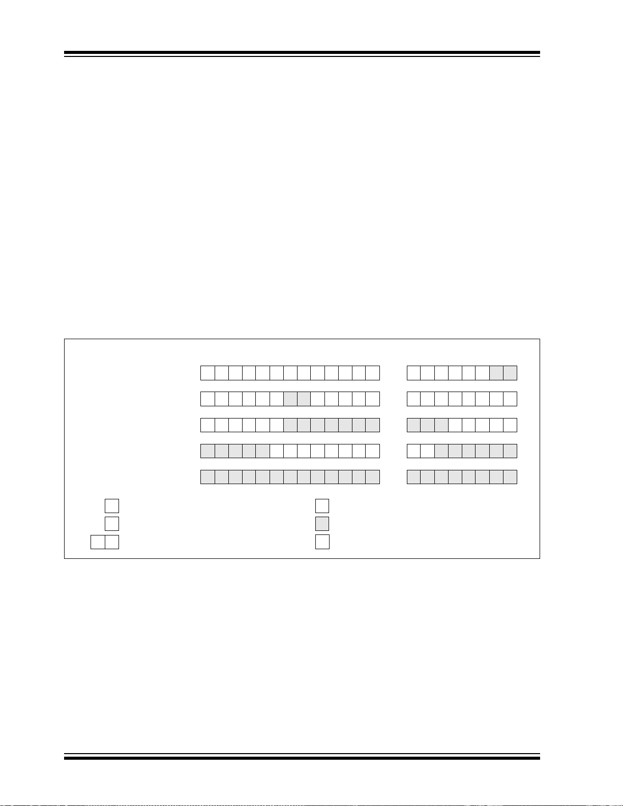
ENC424J600/624J600
T XX 01 02 03 04 05 8A 8B 8C H
...
Initial state, buffer is empty:
05 06 07 08 0A H T XX 01 02 03 04
...
Buffer has wrapped and
contains pending data:
T XX H
...
H T
XX
...
Buffer is empty:
Buffer contains pending
data to be processed:
92 93 94 95 96 97 98 99 H T XX 01 02 8A 8B 8C 8D 8E 8F 90 91
...
Buffer has wrapped
and is currently full:
H
T
XX
01 02
Free byte for incoming data
Byte protected from incoming data
Head Pointer (ERXHEAD)
Tail Pointer (ERXTAIL), skip when reading
Dummy byte, skip when reading
Next Packet Pointer for pending frame
ERXST 5FFFh
In full duplex, the MAC inhibits transmission of any
packets until the pause timer expires when two
conditions are met:
• Flow control is enabled (RXPAUS bit is set) and
• A valid pause frame was received from the
remote node
It will still be possible for software to set the TXRTS bit
to start a transmission. However, this has the effect of
queuing the packet for future transmission instead of
causing an immediate transmission to start. Once the
pause timer expires, the queued packet will transmit
normally, causing any applicable interrupts to occur.
Each frame starts on an even address. The hardware
maintains a Receive Head Pointer, ERXHEAD, indicating
the next location to be written, and automatically wraps
back to ERXST when it reaches the end of memory. The
Tail Pointer, ERXTAIL, is maintained by software.
Addresses from the Tail Pointer, up to the Head Pointer,
are considered to be protected by software. This allows
the host controller to prevent incoming frames from
overwriting data that has not yet been processed.
When ERXTAIL points to the same location as
ERXHEAD, the receive packet buffer is considered to
be full. Due to this definition, there is no empty condition. For simplicity, applications may choose to keep
the Tail Pointer always set to two bytes behind the next
9.2 Receiving Packets
As Ethernet frames arrive, they are written to the circular receive buffer, bounded by the Receive Buffer Start
Address (ERXST) register and the end of the physical
memory at 5FFFh. The hardware also maintains a
counter indicating the number of pending frames.
frame to be processed, or two bytes behind the Head
Pointer when no frames are pending. Figure 9-3 shows
these pointer relationships.
If ERXHEAD reaches ERXTAIL while receiving a
frame, or if the receive filters reject the packet, the
ERXHEAD Pointer is rolled back to its previous location
and the packet is discarded.
FIGURE 9-3: EXAMPLES OF RECEIVE BUFFER WRAP BETWEEN ERXHEAD AND ERXTAIL
DS39935C-page 86 2010 Microchip Technology Inc.

ENC424J600/624J600
It is possible for the host application to write to the
receive buffer. However, it is recommended not to do
so outside of the area protected by the Tail Pointer in
order to prevent it from being subsequently overwritten
by future receive packets.
ERXHEAD is a read-only register and may be updated
at any time by hardware. The high byte is shadowed to
ensure it can be safely read on 8-bit interfaces (SPI or
PSP). When reading ERXHEAD, read the low byte first.
This operation simultaneously copies the high byte to a
shadow register. Reading the high byte automatically
reads from this shadow register. This ensures that the
value has not been modified since the low byte was
obtained, even if another packet has been received in
the interim.
9.2.1 CONFIGURING PACKET RECEPTION
Once the MAC and PHY are properly initialized, the
device is ready to begin receiving packets.
To enable reception:
1. Program the ERXST Pointer (low byte first if
writing a byte at a time) to the first address to be
used for the receive buffer. This pointer must
indicate an even address. The Head Pointer,
ERXHEAD, will automatically be set to the same
value.
2. In the host controller application, create a
variable,
address value of the next received packet.
Initialize this variable to be equal to the current
value of ERXST.
3. Program the Tail Pointer, ERXTAIL, to the last
even address of the buffer or 5FFEh.
4. Configure interrupts as desired. See
Section 13.0 “Interrupts” for more information.
5. Set RXEN (ECON1<0>) to enable reception.
Once RXEN is set, it is recommended that ERXST not
be modified. The host controller must monitor the
ENCX24J600 to determine when a packet has arrived
and is ready to be processed. This is accomplished by
using the packet pending interrupt as described in
Section 13.1.5 “Received Packet Pending”.
Alternatively, poll the PKTCNT bits for a non-zero
value.
NextPacketPointer, to hold the
9.2.2 STORAGE OF INCOMING PACKETS
Packets are stored sequentially in the receive buffer.
Each frame is stored as it was presented to the MAC,
including all padding and frame check (CRC) bytes, but
excluding any preamble or start of stream/frame delimiter bytes. Frames are always saved starting on an
even address, so those with an odd length skip one
byte before the next frame begins. A sample packet
stored in memory is shown in Figure 9-4.
When a packet is received, the hardware increments
the Packet Counter bits, PKTCNT (ESTAT<7:0>).
Incoming bytes are written sequentially, beginning at
the Head Pointer, ERXHEAD. If the Head Pointer
reaches the Tail Pointer, ERXTAIL, during reception, or
if incrementing the PKTCNT bits would cause an overflow, the packet will be discarded and the Head Pointer
restored.
Each received frame is preceded in memory by a
pointer to the next frame and a Receive Status Vector
(RSV). The RSV includes the length of the frame, and
flags indicating the type of packet and which filters
were matched. This format of the RSV is shown in
Table 9-1.
To retrieve a packet from the buffer:
1. Verify that a packet is waiting by ensuring that
the PKTCNT<7:0> bits are non-zero or that
PKTIF (EIR<6>) is set.
2. Begin reading at address pointed to by the
application variable,
(see Section 9.2.1 “Configuring Packet
Reception”).
3. Read the first two bytes of the packet, which are
the address of the next packet and write to
NextPacketPointer.
4. Read the next six bytes, which are the Receive
Status Vector (RSV).
5. Read the Ethernet frame. The number of bytes
to be read is indicated by the received byte
count in the RSV read during step 4.
6. As the frame is read and processed, incremental
amounts of memory buffer can be freed up by
updating the ERXTAIL Pointer value to the point
where the packet has been processed, taking
care to wrap back at the end of the received
memory buffer. Once the whole frame has been
processed, the final value of ERXTAIL should be
equal to (
7. Set PKTDEC (ECON1<8>) to decrement the
PKTCNT bits. PKTDEC is automatically cleared
by hardware if PKTCNT decrements to zero.
NextPacketPointer – 2).
NextPacketPointer
2010 Microchip Technology Inc. DS39935C-page 87

ENC424J600/624J600
:
:
:
:
FCS[2] FCS[3]
FCS[0] FCS[1]
01h 68h
RSV[1] RSV[0]
04h 00h
00h A3h
02h 01h
34h 12h
78h 56h
BCh 9Ah
00h 80h
data[1] data[0]
PAD PAD
PAD PAD
XX XX
RSV[3] RSV[2]
RSV[5] RSV[4]
:
:
:
:
PAD data[40]
FCS[2] FCS[3]
FCS[0] FCS[1]
RSV[1] RSV[0]
RSV[3] RSV[2]
Memory
High
Low
Byte Address Byte Address
:
:
011Dh
011Fh
0121h
0123h
0125h
0127h
0129h
012Bh
012Dh
012Fh
0131h
0133h
0135h
0137h
:
:
015Fh
0161h
0163h
0165h
0167h
0169h
016Bh
016Dh
016Fh
:
:
RSV[5] RSV[4]
:
:
011Eh
0120h
0122h
0124h
0126h
0128h
012Ah
012Ch
012Eh
0130h
0132h
0134h
0136h
015Eh
:
:
0160h
0162h
0164h
0166h
0168h
016Ah
016Ch
016Eh
:
:
Previous
Packet
Current
Packet
Next
Packet
ERXTAIL
Pointer to Next Packet
Receive
Status
Vector
Destination
Address
Source
Address
:
:
:
:
011Ch
Start of Next Packet
FIGURE 9-4: EXAMPLE OF A RECEIVED PACKET IN BUFFER MEMORY
DS39935C-page 88 2010 Microchip Technology Inc.

ENC424J600/624J600
TABLE 9-1: RECEIVE STATUS VECTOR
Byte Bit(s) Field Description
5 47:40 Zeros 00h
439Zero ‘0’
38 Reserved
37 Reserved
36 Unicast Filter Match Current frame met criteria for the Unicast Receive filter.
35 Pattern Match Filter Match Current frame met criteria for the Pattern Match Receive filter as
configured when the packet was received.
34 Magic Packet™ Filter Match Current frame met criteria for the Magic Packet Receive filter as
configured when the packet was received.
33 Hash Filter Match Current frame met criteria for the Hash Receive filter as
configured when the packet was received.
32 Not-Me Filter Match Current frame met criteria for the Not-Me Receive filter.
3 31 Runt Filter Match Current frame met criteria for the Runt Packet Receive filter.
30 Receive VLAN Type Detected Current frame was recognized as a VLAN tagged frame.
29 Receive Unknown Opcode Current frame was recognized as a control frame but it contained
an unknown opcode.
28 Receive Pause Control Frame Current frame was recognized as a control frame containing a
valid pause frame opcode and a valid destination address.
27 Receive Control Frame Current frame was recognized as a control frame for having a
valid type/length designating it as a control frame.
26 Dribble Nibble Indicates that after the end of this packet, an additional 1 to 7 bits
were received. The extra bits were thrown away.
25 Receive Broadcast Packet Current frame has a valid Broadcast address.
24 Receive Multicast Packet Current frame has a valid Multicast address.
2 23 Received Ok Received packet had a valid CRC and no symbol errors.
22 Length Out of Range Frame type/length field was larger than 1500 bytes (type field).
21 Length Check Error Frame length field value in the packet does not match the actual
data byte length and specifies a valid length.
20 CRC Error Frame CRC field value does not match the CRC calculated by the
MAC.
19 Reserved
18 Carrier Event Previously Seen A carrier event was detected at some time since the last receive.
The carrier event is not associated with this packet. A carrier event
is activity on the receive channel that does not result in a packet
receive attempt being made.
17 Reserved
16 Packet Previously Ignored A frame larger than 50,000 bit times occurred or a packet has
been dropped since the last receive.
1 15:0 Received Byte Count Length of the received frame in bytes. This includes the
0
destination address, source address, type/length, data, padding
and CRC fields. This field is stored in little-endian format.
2010 Microchip Technology Inc. DS39935C-page 89

ENC424J600/624J600
REGISTER 9-1: ECON1: ETHERNET CONTROL REGISTER 1
R/W-0 R/W-0 R/W-0 R/W-0 R/W-0 R/W-0 R/W-0 R/W-0
MODEXST HASHEN HASHOP HASHLST AESST AESOP1 AESOP0 PKTDEC
bit 15 bit 8
R/W-0 R/W-0 R/W-0 R/W-0 R/W-0 R/W-0 R/W-0 R/W-0
FCOP1 FCOP0 DMAST DMACPY DMACSSD DMANOCS TXRTS RXEN
bit 7 bit 0
Legend:
R = Readable bit W = Writable bit U = Unimplemented bit, read as ‘0’
-n = Value at POR ‘1’ = Bit is set ‘0’ = Bit is cleared x = Bit is unknown
bit 15 MODEXST: Modular Exponentiation Start bit
1 = Modular exponentiation calculation started/busy; automatically cleared by hardware when done
0 = Modular exponentiation calculation done/Idle
bit 14 HASHEN: MD5/SHA-1 Hash Enable bit
1 = MD5/SHA-1 hashing engine enabled. Data written to the hashing engine by the DMA is added to
the hash.
0 = MD5/SHA-1 hashing engine disabled
bit 13 HASHOP: MD5/SHA-1 Hash Operation Control bit
1 = MD5/SHA-1 hash engine loads the Initial Value (IV) from the hash memory. This mode is typically
used for HMAC hash operations.
0 = Normal MD5/SHA-1 hash operation
bit 12 HASHLST: MD5/SHA-1 Hash Last Block Control bit
1 = The next DMA transfer to the hash engine completes the hash. If needed, padding is automatically
generated and added to the hash.
0 = The next DMA transfer to the hash engine adds data to the hash. Further data additions to the hash
are still possible.
bit 11 AESST: AES Encrypt/Decrypt Start bit
1 = AES encrypt/decrypt operation is started/busy; automatically cleared by hardware when done
0 = AES encrypt/decrypt operation is done/Idle
bit 10-9 AESOP<1:0>: AES Operation Control bits
11 = Reserved
10 = ECB/CBC decrypt
01 = CBC/CFB encrypt
00 = ECB/CFB/OFB encrypt or key initialization
bit 8 PKTDEC: RX Packet Counter Decrement Control bit
1 = Decrement PKTCNT (ESTAT<7:0>) bits by one. Hardware immediately clears PKTDEC to ‘0’,
allowing back-to-back decrement operations.
0 = Leave PKTCNT bits unchanged
bit 7-6 FCOP<1:0>: Flow Control Operation Control/Status bits
When FULDPX (MACON2<0>) =
11 = End flow control by sending a pause frame with 0000h pause timer value; automatically cleared
by hardware when done
10 = Enable flow control by periodically sending pause frames with a pause timer defined by EPAUS
01 = Transmit single pause frame defined by EPAUS; automatically cleared by hardware when done
00 = Flow control disabled/Idle
When FULDPX (MACON2<0>) =
1x, 01 = Enable flow control by continuously asserting backpressure (transmitting preamble)
00 = Flow control disabled/Idle
1:
0:
DS39935C-page 90 2010 Microchip Technology Inc.

ENC424J600/624J600
REGISTER 9-1: ECON1: ETHERNET CONTROL REGISTER 1 (CONTINUED)
bit 5 DMAST: DMA Start bit
1 = DMA is started/busy; automatically cleared by hardware when done
0 = DMA is done/Idle
bit 4 DMACPY: DMA Copy Control bit
1 = DMA copies data to memory location at EDMADST
0 = DMA does not copy data; EDMADST is ignored
bit 3 DMACSSD: DMA Checksum Seed Control bit
1 = DMA checksum operations are initially seeded by the one’s complement of the checksum
contained in EDMACS
0 = DMA checksum operations are initially seeded by 0000h
bit 2 DMANOCS: DMA No Checksum Control bit
1 = DMA does not compute checksums; EDMACS remains unchanged
0 = DMA computes checksums; hardware updates EDMACS at the completion of all DMA operations
bit 1 TXRTS: Transmit Request to Send Status/Control bit
1 = Transmit an Ethernet frame; automatically cleared by hardware when done
0 = Transmit logic done/Idle
bit 0 RXEN: Receive Enable bit
1 = Packets which pass the current RX filter configuration are written to the receive buffer
0 = All packets received are ignored
2010 Microchip Technology Inc. DS39935C-page 91

ENC424J600/624J600
REGISTER 9-2: ETXSTAT: ETHERNET TRANSMIT STATUS REGISTER
U-0 U-0 U-0 R-0 R-0 R-0 R-0 R-0
— — — r rLATECOL
(1)
MAXCOL
bit 15 bit 8
R-0 R-0 R-0 R-0 R-0 R-0 R-0 R-0
DEFER
(1)
r r CRCBAD COLCNT3
(1)
COLCNT2
(1)
COLCNT1
bit 7 bit 0
Legend:
R = Readable bit W = Writable bit U = Unimplemented bit, read as ‘0’
-n = Value at POR ‘1’ = Bit is set ‘0’ = Bit is cleared x = Bit is unknown
bit 15-13 Unimplemented: Read as ‘0’
bit 12-11 Reserved: Ignore on read
bit 10 LATECOL: Transmit Late Collision Status bit
(1)
1 = A collision occurred after transmitting more than MACLCONH + 8 bytes. The last transmission was
aborted.
0 = No late collision occurred during the last transmission
bit 9 MAXCOL: Transmit Maximum Collisions Status bit
(1)
1 = MACLCONL + 1 collisions occurred while transmitting the last packet. The last transmission was
aborted.
0 = MACLCONL or less collisions occurred while transmitting the last packet
bit 8 EXDEFER: Transmit Excessive Defer Status bit
(1)
1 = The medium was busy with traffic from other nodes for more than 24,288 bit times. The last
transmission was aborted.
0 = The MAC deferred for less than 24,288 bit times while transmitting the last packet
bit 7 DEFER: Transmit Defer Status bit
(1)
1 = The medium was busy with traffic from other nodes, so the MAC was forced to temporarily defer
transmission of the last packet
0 = No transmit deferral or an excessive deferral occurred while attempting to transmit the last packet
bit 6-5 Reserved: Ignore on read
bit 4 CRCBAD: Transmit CRC Incorrect Status bit
1 = The FCS field of the last packet transmitted did not match the CRC internally generated by the
MAC during transmission
0 = The FCS field of the last packet transmitted was correct or the MAC is configured to append an
internally generated CRC
bit 3-0 COLCNT<3:0>: Transmit Collision Count Status bits
(1)
Number of collisions that occurred while transmitting the last packet.
(1)
(1)
EXDEFER
COLCNT0
(1)
(1)
Note 1: Applicable in Half-Duplex mode only; collisions and deferrals are not possible in Full-Duplex mode.
DS39935C-page 92 2010 Microchip Technology Inc.

ENC424J600/624J600
REGISTER 9-3: ESTAT: ETHERNET STATUS REGISTER
R-0 R-0 R-0 R-0 R-0 R-0 R-0 R-0
INT FCIDLE RXBUSY CLKRDY
bit 15 bit 8
R-0 R-0 R-0 R-0 R-0 R-0 R-0 R-0
PKTCNT7 PKTCNT6 PKTCNT5 PKTCNT4 PKTCNT3 PKTCNT2 PKTCNT1 PKTCNT0
bit 7 bit 0
Legend:
R = Readable bit W = Writable bit U = Unimplemented bit, read as ‘0’
-n = Value at POR ‘1’ = Bit is set ‘0’ = Bit is cleared x = Bit is unknown
bit 15 INT: Interrupt Pending Status bit
1 = One of the EIR bits is set and enabled by the EIE register. If INTIE (EIE<15>) is set, the INT
also driven low.
0 = No enabled interrupts are currently pending. The INT pin is being driven high.
bit 14 FCIDLE: Flow Control Idle Status bit
1 = Internal flow control state machine is Idle. It is safe to change the FCOP (ECON1<7:6>) and
FULDPX (MACON2<0>) bits.
0 = Internal flow control state machine is busy. Do not modify the FCOP (ECON1<7:6>) or FULDPX
(MACON2<0>) bits.
bit 13 RXBUSY: Receive Logic Active Status bit
1 = Receive logic is currently receiving a packet. This packet may be discarded in the future if an RX
buffer overflow occurs or a receive filter rejects it, so this bit does not necessarily indicate that an
RX packet pending interrupt will occur.
0 = Receive logic is Idle
bit 12 CLKRDY: Clock Ready Status bit
1 = Normal operation
0 = Internal Ethernet clocks are not running and stable yet. Only the ESTAT and EUDAST registers
should be accessed.
bit 11 Reserved: Ignore on read
bit 10 PHYDPX: PHY Full Duplex Status bit
1 = PHY is operating in Full-Duplex mode
0 = PHY is operating in Half-Duplex mode
bit 9 Reserved: Ignore on read
bit 8 PHYLNK: PHY Linked Status bit
1 = Ethernet link has been established with a remote Ethernet partner
0 = No Ethernet link present
bit 7-0 PKTCNT<7:0>: Receive Packet Count bits
Number of complete packets that are saved in the RX buffer and ready for software processing. Set the
PKTDEC (ECON1<8>) bit to decrement this field.
r PHYDPX rPHYLNK
pin is
2010 Microchip Technology Inc. DS39935C-page 93

ENC424J600/624J600
NOTES:
DS39935C-page 94 2010 Microchip Technology Inc.

ENC424J600/624J600
10.0 RECEIVE FILTERS
To minimize the number of frames that the host controller
must process, ENC424J600/624J600 devices incorporate 11 different receive filters to discard unwanted
frames. The following filters are available:
• CRC Error Collection Filter
• Runt Error Collection Filter
• CRC Error Rejection Filter
• Runt Error Rejection Filter
• Unicast Collection Filter
• Not-Me Unicast Collection Filter
• Multicast Collection Filter
• Broadcast Collection Filter
• Hash Table Collection Filter
• Magic Packet™ Collection Filter
• Pattern Match Collection Filter
Each filter is software configurable, and can be individually enabled or disabled, using the ERXFCON register
(Register 10-1). Each filter is either a Collection or a
Rejection filter, with incoming frames passing sequentially through each enabled filter. The first filter to make a
definitive decision for a frame takes priority over all
others. Collection filters either force a frame to be
accepted or defer the decision to a lower priority filter.
Similarly, Rejection filters either discard frames or defer
to lower priority filters. Frames that pass through all filters
without specifically being accepted are discarded.
Figure 10-1 demonstrates this decision tree.
At power-up, the CRC Error Rejection, Runt Error
Rejection, Unicast Collection and Broadcast Collection
filters are enabled, and all others are disabled. With
these settings, the device will only accept Broadcast
frames and frames specifically addressed to the local
MAC address. Invalid frames and those destined for
other nodes will be automatically rejected.
Note 1: The MAC internally processes and filters
Ethernet control frames as they arrive
and before they reach these filters. For
the application to receive Ethernet control
frames, enable the PASSALL option
(MACCON1<1> =
2: If the Ethernet Receive Enable bit, RXEN
(ECON1<0>), is set, the filters may make
an incorrect decision if any of the receive
filters are reconfigured at the exact
moment a new frame is being received.
To avoid this behavior, clear the RXEN bit
prior to changing any receive filter
settings.
1).
2010 Microchip Technology Inc. DS39935C-page 95

ENC424J600/624J600
REGISTER 10-1: ERXFCON: ETHERNET RX FILTER CONTROL REGISTER
R/W-0 R/W-0 U-0 R/W-0 R/W-0 R/W-0 R/W-0 R/W-0
HTEN MPEN
bit 15 bit 8
R/W-0 R/W-1 R/W-0 R/W-1 R/W-1 R/W-0 R/W-0 R/W-1
CRCEEN CRCEN RUNTEEN RUNTEN UCEN NOTMEEN MCEN BCEN
bit 7 bit 0
Legend:
R = Readable bit W = Writable bit U = Unimplemented bit, read as ‘0’
-n = Value at POR ‘1’ = Bit is set ‘0’ = Bit is cleared x = Bit is unknown
— NOTPM PMEN3 PMEN2 PMEN1 PMEN0
bit 15 HTEN: Hash Table Collection Filter Enable bit
1 = Accept packets having a hashed destination address that points to a set bit in the Hash Table
0 = Filter is disabled
bit 14 MPEN: Magic Packet™ Collection Filter Enable bit
1 = Accept packets containing a Magic Packet pattern for the local MAC address
0 = Filter is disabled
bit 13 Unimplemented: Read as ‘0’
bit 12 NOTPM: Pattern Match Inversion Control bit
1 = Pattern Match checksum mismatch required for a successful Pattern Match
0 = Pattern Match checksum match required for a successful Pattern Match
bit 11-8 PMEN<3:0>: Pattern Match Collection Filter Enable bits
When NOTPM =
0:
A packet is accepted by the filter if the pattern checksum matches AND the selected mode’s condition is
true.
When NOTPM =
1:
A packet is accepted by the filter if pattern checksum does not match AND the selected mode’s condition
is true.
1111
.... = Reserved
1010
1001 = Magic Packet for local Unicast address
(1)
1000 = Hashed packet destination points to a bit in the Hash Table registers that is set
0111 = Packet destination is not the Broadcast address
0110 = Packet destination is the Broadcast address
0101 = Packet destination is not a Multicast address
0100 = Packet destination is a Multicast address
(1)
(1)
(1)
0011 = Packet destination is not the local Unicast address
0010 = Packet destination is the local Unicast address
0001 = Accept all packets with a checksum match defined by NOTPM
0000 = Filter is disabled
bit 7 CRCEEN: CRC Error Collection Filter Enable bit
1 = Packets with an invalid CRC will be accepted, regardless of all other filter settings
0 = Filter is disabled
(1)
(1)
(1)
(1)
(1)
(1)
(1)
Note 1: This filtering decision can be overridden by the CRC Error Rejection filter and Runt Error Rejection filter
decisions, if enabled, by CRCEN or RUNTEN.
2: This filtering decision can be overridden by the CRC Error Collection filter and Runt Error Collection filter
decisions, if enabled, by CRCEEN or RUNTEEN.
DS39935C-page 96 2010 Microchip Technology Inc.

ENC424J600/624J600
REGISTER 10-1: ERXFCON: ETHERNET RX FILTER CONTROL REGISTER (CONTINUED)
bit 6 CRCEN: CRC Error Rejection Filter Enable bit
1 = Packets with an invalid CRC will be discarded
0 = Filter is disabled
bit 5 RUNTEEN: Runt Error Collection Filter Enable bit
1 = Accept packets that are 63 bytes or smaller, regardless of all other filter settings
0 = Filter is disabled
bit 4 RUNTEN: Runt Error Rejection Filter Enable bit
1 = Discard packets that are 63 bytes or smaller
0 = Filter is disabled
bit 3 UCEN: Unicast Destination Collection Filter Enable bit
1 = Accept packets with a destination address matching the local MAC address
0 = Filter is disabled
bit 2 NOTMEEN: Not-Me Unicast Destination Collection Filter Enable bit
1 = Accept packets with a Unicast destination address that does not match the local MAC address
0 = Filter is disabled
bit 1 MCEN: Multicast Destination Collection Filter Enable bit
1 = Accept packets with a Multicast destination address
0 = Filter is disabled
bit 0 BCEN: Broadcast Destination Collection Filter Enable bit
1 = Accept packets with a Broadcast destination address of FF-FF-FF-FF-FF-FF
0 = Filter is disabled
Note 1: This filtering decision can be overridden by the CRC Error Rejection filter and Runt Error Rejection filter
decisions, if enabled, by CRCEN or RUNTEN.
2: This filtering decision can be overridden by the CRC Error Collection filter and Runt Error Collection filter
decisions, if enabled, by CRCEEN or RUNTEEN.
(2)
(2)
(1)
(1)
(1)
(1)
2010 Microchip Technology Inc. DS39935C-page 97

ENC424J600/624J600
Packet Arrives
Discard Packet Accept Packet
HTEN set?
CRC is valid?
MPEN set?
Pattern
Match?
(1)
CRCEEN set?
CRCEN set?
RUNTEEN set?
RUNTEN set?
UCEN set?
BCEN set?
MCEN set?
NOTMEEN set?
Yes
No
No
No
No
No
No
No
No
No
No
Reject or
Disabled
Length < 64
bytes?
CRC is valid?
Length < 64
bytes?
Unicast for me?
Unicast for
someone else?
Multicast
destination?
Broadcast
destination?
Hash Table
bit set?
Magic Packet™
for me?
Yes
Yes
Yes
Yes
Yes
Yes
Yes
Yes
Yes
Yes
Yes
Yes
Yes
Yes
Yes
No
No
No
No
No
No
No
No
Yes
Yes
No
No
Accept
Yes
Yes
Note 1: For details on the Pattern Match filter, refer to Section 10.11 “Pattern Match Collection Filter”.
FIGURE 10-1: RECEIVE FILTER DECISION TREE
DS39935C-page 98 2010 Microchip Technology Inc.
 Loading...