

Page 1

ENC28J60
Data Sheet
Stand-Alone Ethernet Controller
with SPI™ Interface
2004 Microchip Technology Inc. Advance Information DS39662A
Page 2

Note the following details of the code protection feature on Microchip devices:
• Microchip products meet the specification contained in their particular Microchip Data Sheet.
• Microchip believes that its family of products is one of the most secure families of its kind on the market today, when used in the
intended manner and under normal conditions.
• There are dishonest and possibly illegal methods used to breach the code protection feature. All of these methods, to our
knowledge, require using the Microchip products in a manner outside the operating specifications contained in Microchip’s Data
Sheets. Most likely, the person doing so is engaged in theft of intellectual property.
• Microchip is willing to work with the customer who is concerned about the integrity of their code.
• Neither Microchip nor any other semiconductor manufacturer can guarantee the security of their code. Code protection does not
mean that we are guaranteeing the product as “unbreakable.”
Code protection is constantly evolving. We at Microchip are committed to continuously improving the code protection features of our
products. Attempts to break Microchip’s code protection feature may be a violation of the Digit al Millennium Copyright Act. If suc h a c t s
allow unauthorized access to your software or other copyrighted work, you may have a right to sue for relief under that Act.
Information contained in this publication regarding device
applications and the like is provided only for your convenience
and may be superseded by updates. It is your responsibility to
ensure that your application meets with your specifications.
MICROCHIP MAKES NO REPRESENTATIONS OR WARRANTIES OF ANY KIND WHETHER EXPRESS OR IMPLIED,
WRITTEN OR ORAL, STATUTORY OR OTHERWISE,
RELATED TO THE INFORMATION, INCLUDING BUT NOT
LIMITED TO ITS CONDITION, QUALITY, PERFORMANCE,
MERCHANTABILITY OR FITNESS FOR PURPOSE.
Microchip disclaims all liability arising from this information and
its use. Use of M icrochip’s prod ucts as critical components in
life support systems is not authorized except with express
written approval by Microchip. No licenses are conveyed,
implicitly or otherwise, under any Microchip intellectual property
rights.
Trademarks
The Microchip name and logo, the Microchip logo, Accuron,
dsPIC, K
EELOQ, microID, MPLAB, PIC, PICmicro, PICSTART,
PRO MATE, PowerSmart, rfPIC, and SmartShunt are
registered trademarks of Microchip Technology Incorporated
in the U.S.A. and other countries.
AmpLab, FilterLab, Migratable Memory, MXDEV, MXLAB,
PICMASTER, SEEVAL, SmartSensor and The Embedded
Control Solutions Company are registered trademarks of
Microchip Technology Incorporated in the U.S.A.
Analog-for-the-Digital Age, Application Maestro, dsPICDEM,
dsPICDEM.net, dsPICworks, ECAN, ECONOMONITOR,
FanSense, FlexROM, fuzzyLAB, In-Circuit Serial
Programmin g, IC SP, ICEPI C, M PASM, MPLIB, MPLINK,
MPSIM, PICkit, PICDEM, PICDEM.net, PICLAB, PICtail,
PowerCal, PowerInfo, PowerMate, PowerTool, rfLAB,
rfPICDEM, Select Mode, Smart Serial, SmartT el and Total
Endurance are trademarks of Microchip Technology
Incorporated in the U.S.A. and other countries.
SQTP is a service mark of Microchip Technology Incorporated
in the U.S.A.
All other trademarks mentioned herein are property of their
respective companies.
© 2004, Microchip Technology Incorporated, Printed in the
U.S.A., All Rights Reserved.
Printed on recycled paper.
Microchip received ISO/TS-16949:2002 quality system certification for
its worldwide headquarters, design and wafer fabrication facilities in
Chandler and Tempe, Arizona and Mountain View, California in
October 2003. The Company’s quality system processes and
procedures are for its PICmicro
devices, Serial EEPROMs, microperipherals, nonvolatile memory and
analog products. In addition, Microchip’s quality system for the design
and manufacture of development systems is ISO 9001:2000 certified.
®
8-bit MCUs, KEELOQ
®
code hopping
DS39662A-page ii Advance Information 2004 Microchip Technology Inc.
Page 3
ENC28J60
Stand-Alone Ethernet Controller with SPI™ Interface
Ethernet Controller Features
• IEEE 802.3 compatible Ethernet controller
• Integrated MAC and 10BASE-T PHY
• Receiver and collision squelch circuit
• Supports one 10BASE-T port with automatic
polarity detection and correction
• Supports Full and Half-Duplex modes
• Programmable automatic retransmit on collision
• Programmable padding and CRC generation
• Programmable automatic rejection of erroneous
packets
• SPI™ Interface with speeds up to 10 Mb/s
Buffer
• 8-Kbyte transmit/receive packet dual port SRAM
• Configurable transmit/receive buffer size
• Hardware-managed circular receive FIFO
• Byte-wide random and sequential access with
auto-increment
• Internal DMA for fast data movement
• Hardware assisted IP checksum calculation
Medium Access Controller (MAC) Features
• Supports Unicast, Multicast and Broadcast
packets
• Programmable receive packet filtering and
wake-up host on logical AND or OR of the
following:
- Unicast destination address
- Multicast address
- Broadcast address
- Magic Packet™
- Group destination addresses as defined by
64-bit hash table
- Programmable pattern matching of up to
64 bytes at user-defined offset
• Loopback mode
Physical Layer (PHY) Features
Operational
• Two programmable LED outputs for LINK, TX,
RX, collision and full/half-duplex status
• Seven interrupt sources with two interrupt pins
•25MHz clock
• Clock out pin with programmable prescaler
• Operating voltage range of 3.14V to 3.45V
• TTL level inputs
• Temperature range: -40°C to +85°C Industrial,
0°C to +70°C Commercial (SSOP only)
• 28-pin SPDIP, SSOP, SOIC, QFN packages
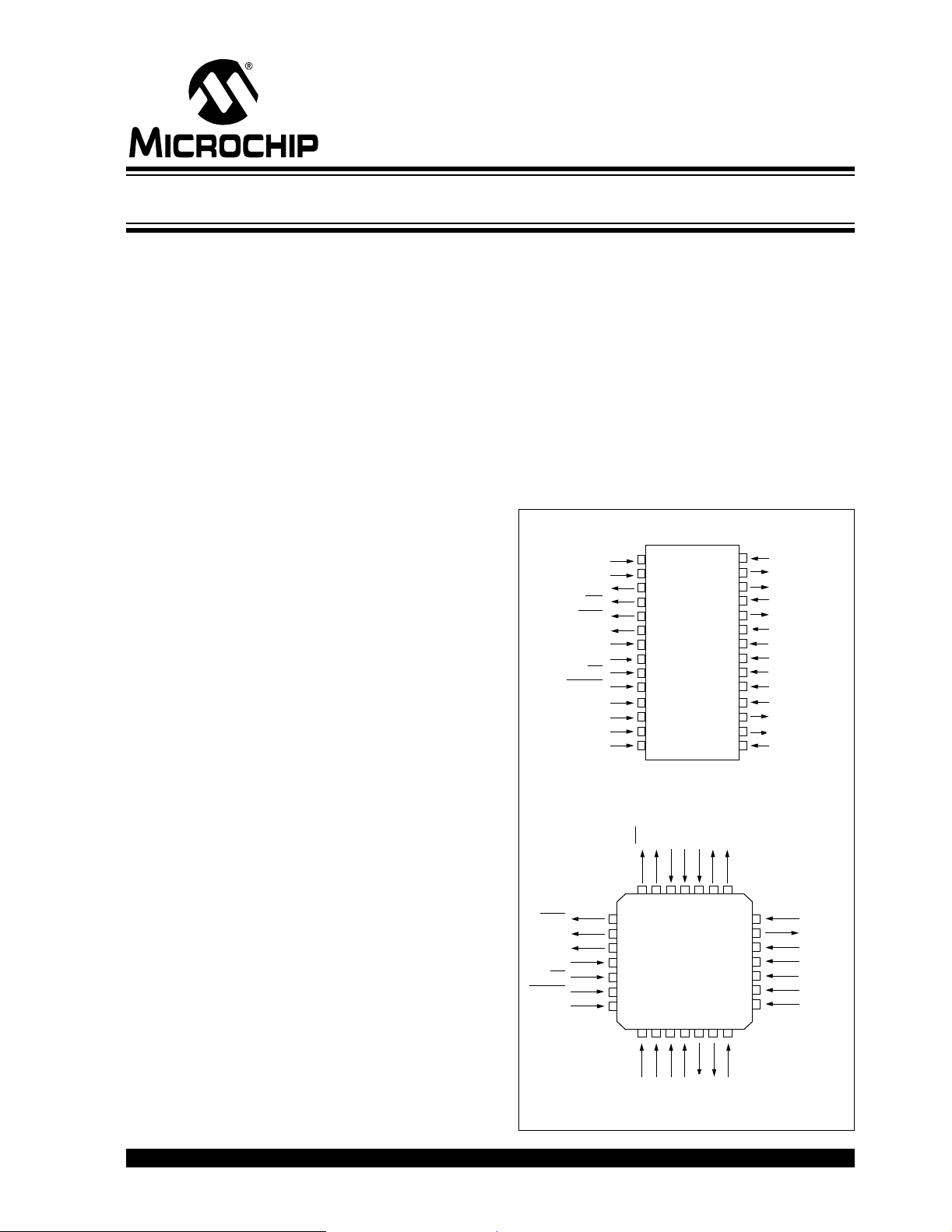
Package Types
28-Pin SPDIP, SSOP, SOIC
V
VCAP
CLKOUT
WOL
SCK
RESET
VSSRX
TPIN-
TPIN+
RBIAS
28-pin QFN
WOL
SO
SI
SCK
CS
RESET
VSSRX
VSS
INT
SO
CS
SI
1
2
3
4
5
6
7
1
2
3
4
5
6
7
8
9
10
11
12
13
14
INT
28 27 26 25 2423 22
CLKOUT
VSS
ENC28J60
LEDA
VCAP
VDD
ENC28J60
8910
1112 13 14
28
27
26
25
24
23
22
21
20
19
18
17
16
15
LEDB
DD
LEDA
LEDB
V
DDOSC
OSC2
OSC1
VSSOSC
VSSPLL
VDDPLL
DDRX
V
VSSTX
TPOUT+
TPOUTVDDTX
21
20
19
18
17
16
15
VDDOSC
OSC2
OSC1
VSSOSC
VSSPLL
VDDPLL
VDDRX
• Wave shapi ng out put filter
• Loopback mode
TPIN-
TPIN+
RBIAS
2004 Microchip Technology Inc. Advance Information DS39662A-page 1
VSSTX
VDDTX
TPOUT-
TPOUT+
Page 4

ENC28J60
Table of Contents
1.0 Overview ......................................................................................................................................................................................3
2.0 External Connections ...................................................................................................................................................................5
3.0 Memory Organization................................................................................................................................................................. 11
4.0 Serial Peripheral Interface (SPI). ................................................................................................................................................25
5.0 Ethernet Overview......................................................... ..................... ..................... ................................................................... 31
6.0 Initialization................................................................................................................................................................................. 33
7.0 Transmitting and Receiving Packets.......................................................................................................................................... 39
8.0 Receive Filters............................................................................................................................................................................ 47
9.0 Duplex Mode Configuration and Negotiation.............................................................................................................................. 53
10.0 Flow Control............................................................................................................................................................................... 55
11.0 Reset.......................................................................................................................................................................................... 59
12.0 Interrupts....................................................................................................................................................................................65
13.0 Direct Memory Access Controller.......................................... ..................... ..................... ...........................................................75
14.0 Power-Down............................................................................................................................................................................... 77
15.0 Built-in Self-Test Controller ........................................................................................................................................................79
16.0 Electrical Characteristics............................................................................................................................................................83
17.0 Packaging Information.......................... ..................... ..................... ............................................................................................ 89
Index .................................................................................................................................................................................................... 95
On-Line Support........................................................................ .. .... .. ......... .... .. .... ......... .. ..................................................................... 97
Systems Information and Upgrade Hot Line........................................................................................................................................ 97
Reader Response................................................................................................................................................................................ 98
Product Identification System............................................................................................................................................................... 99
TO OUR VALUED CUSTOMERS
It is our intention to provide our valued customers with the best documentation possible to ensure successful use of your Microchip
products. To this end, we will continue to improve our publications to better suit your needs. Our publications will be refined and
enhanced as new volumes and updates are introduced.
If you have any questions or c omm ents regarding t his publication, p lease c ontact the M arket ing Co mmunications Department via
E-mail at docerrors@microchip.com or fax the Reader Response Form in the back of this data sheet to (480) 792-4150. We
welcome your feedback.
Most Current Data Sheet
To obtain the most up-to-date version of this data sheet, please register at our Worldwide Web site at:
http://www.microchip.com
You can determine the version of a data sheet by examining its literature number found on the bottom outside corner of any page.
The last character of the literature number is the version number, (e.g., DS30000A is version A of document DS30000).
Errata
An errata sheet, describing minor operational differences from the data sheet and recommended workarounds, may exist for current
devices. As device/documentation issues become known to us, we will publish an errata sheet. The errata will specify the revision
of silicon and revision of document to which it applies.
To determine if an errata sheet exists for a particular device, please check with one of the following:
• Microchip’s Worldwide Web site; http://www.microchip.com
• Your local Microchip sales office (see last page)
When contacting a sales office, please specify which device, revision of silicon and data sheet (include literature number) you are
using.
Customer Notification System
Register on our web site at www.microchip.com to receive the most current information on all of our products.
DS39662A-page 2 Advance Information 2004 Microchip Technology Inc.
Page 5
ENC28J60
1.0 OVERVIEW
The ENC28J60 is a stand-alone Ethernet controller
with an industry standard Serial Peripheral Interface
(SPI™). It is designed to serv e as an Ethe rnet n etw o rk
interface for any controller equipped with SPI.
The ENC28J60 meets all of the IEEE 802.3 specifications. It incorporates a number of packet filtering
schemes to limi t in comi ng packe ts. It also provi des an
internal DMA mod ule for fast data thr oughput and hardware assisted IP checks um calc ulatio ns. Commu nication with the host controller is implemented via two
interrupt pins and the SPI, with data rates of up to
10 Mb/s. Two dedicated pins are used for LED link and
network activity indication.
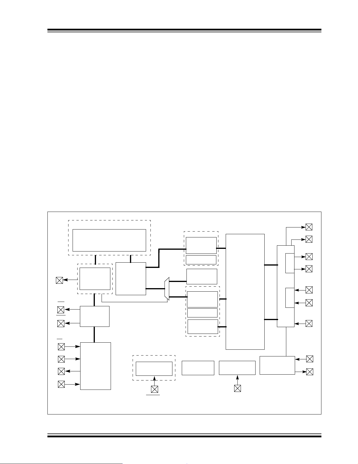
A simple bloc k diagram of the ENC28J60 is shown in
Figure 1-1. A typical applicati on circuit using the dev ice
is shown in Figure 1-2. With the ENC28J60, two pulse
transformers and a few p assive component s are all that
is required to connect a microcontroller to a 10 Mbps
Ethernet network.
FIGURE 1-1: ENC28J60 BLOCK DIAGRAM
The ENC28J60 consists of seven major functional
blocks:
1. An SPI interface that serves as a communica-
tion channel betwee n the host cont roller an d the
ENC28J60.
2. Control Registers which are us ed to cont rol an d
monitor the ENC28J60.
3. A dual port RAM buffer for received and
transmitted data packets.
4. An arbiter to control the access to the RAM
buffer when requests are made from DMA,
transmit and receive blocks.
5. The bus interface that interprets data and
commands received via the SPI interface.
6. The MAC (Medium Access Contro l) module th at
implements IEEE 802.3 compliant MAC logic.
7. The PHY (Physical Layer) module that encodes
and decodes the analog data that is present on
the twisted pair interface.
The device also contains other support blocks, such as
the oscillator, on-chip volt age regulator, level translators
to provide 5V tolerant I/Os and system control logic.
CLKOUT
INT
WOL
(1)
CS
(1)
SI
SO
(1)
SCK
8 Kbytes
Dual Port RAM
Control
Registers
Bus Interface
SPI
Buffer
Arbiter
ch0
ch1
System Control
ch0
ch1
RX
RXBM
RXF (Filter)
DMA &
IP Checksum
TX
TXBM
Flow Control
Host Interface
Power-on
Reset
MAC
Voltage
Regulator
RMII
Interface
MIIM
Interface
PHY
25 MHz
Oscillator
TX
RX
LEDA
LEDB
TPOUT+
TPOUT-
TPIN+
TPIN-
RBIAS
OSC1
OSC2
(1)
RESET
Note 1: These pins are 5V tolerant.
2004 Microchip Technology Inc. Advance Information DS39662A-page 3
VCAP
Page 6
ENC28J60
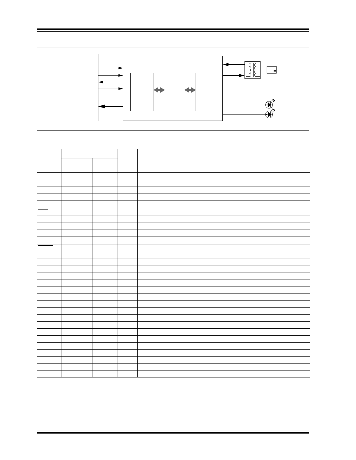
FIGURE 1-2: TYPICAL ENC28J60-BASED INTERFACE
MCU
I/O
SDO
SDI
SCK
INT
CS
SI
SO
SCK
INT
, WOL
X
TX/RX
Buffer
ENC28J60
MAC
PHY
TPIN+/-
TPOUT+/-
TRANSFORMER
LEDA
LEDB
RJ45
ETHERNET
TABLE 1-1: PINOUT I/O DESCRIPTIONS
Pin Number
Pin Name
SPDIP,
SOIC, SSOP
QFN
VCAP 1 25 P — 2.5V output from internal regulator. A 10 µF capacitor to VSSTX must be
VSS 2 26 P — Ground reference.
CLKOUT 3 27 O — Programmable clock output pin.
INT 4 28 O — INT interrupt output pin.
WOL 5 1 O — Wake-up on LAN interrupt out pin.
SO 6 2 O — Data out pin for SPI™ interface.
SI 7 3 I ST Data in pin for SPI interface.
SCK 8 4 I ST Clock in pin for SPI interface.
CS 9 5 I ST Chip select input pin for SPI interface.
RESET 10 6 I ST Active-low device Reset input.
VSSRX 11 7 P — Ground reference for PHY RX.
TPIN- 12 8 I ANA Differential signal input.
TPIN+ 13 9 I ANA Differential signal input.
RBIAS 14 10 I ANA Bias current pin for PHY . Must be tied to VSSRX through a 2 kΩ, 1% resistor.
VDDTX 15 11 P — Positive supply for PHY TX.
TPOUT- 16 12 O — Differential signal output.
TPOUT+ 17 13 O — Differential signal output.
VSSTX 18 14 P — Ground reference for PHY TX.
VDDRX 19 15 P — Positive 3.3V supply for PHY RX.
VDDPLL 20 16 P — Positive 3.3V supply for PHY PLL.
VSSPLL 21 17 P — Ground reference for PHY PLL.
VSSOSC 22 18 P — G round reference for oscillator.
OSC1 23 19 I DIG Oscillator input.
OSC2 24 20 O — Oscillator output.
VDDOSC 25 21 P — Positive 3.3V supply for oscillator.
LEDB 26 22 O — LEDB driver pin.
LEDA 27 23 O — LEDA driver pin.
VDD 28 24 P — Positive 3.3V supply.
Legend: I = Input, O = Output, P = Power, DIG = Digital input, ANA = Analog signal input, ST = Schmitt Trigger
Note 1: Pins have a maximum current capacity of 8 mA.
2: Pins have a maximum current capacity of 4 mA.
3: Pins are 5V tolerant.
4: Pins have an internal weak pull-up to V
5: Pins have a maximum current capacity of 12 mA.
Pin
Type
Buffer
Type
DD.
Description
placed on this pin.
(1)
(2)
(2)
(2)
(3)
(3)
(3,4)
(3, 4)
(5)
(5)
DS39662A-page 4 Advance Information 2004 Microchip Technology Inc.
Page 7

ENC28J60
2.0 EXTERNAL CONNECTIONS
2.1 Oscillator
The ENC28J60 is designed to operate at 25 MHz with
a crystal connected to the OSC1 and OSC2 pins. The
ENC28J60 design requires the use of a parallel cut
crystal. Use of a series cut crystal may give a frequency
out of the crysta l m anu fac ture r sp ec ifi cat ions. A typical
oscillator circuit is shown in Figure 2-1.
The ENC28J60 may als o be driven by a n external clock
source connected to the OSC1 pin as shown in
Figure 2-2.
FIGURE 2-1: CRYSTAL OSCILLATOR
OPERATION
ENC28J60
OSC1
C
1
XTAL
RF
(1)
R
C
S
2
OSC2
To Internal Logic
(2)
2.2 Oscillator Start-up Timer
The ENC28J60 contains an Oscillator Start-up Timer
(OST) to ensure that the oscillator and integrated PHY
have stabilized before use. The OST does not expire
until 7500 OSC1 clock cycles (300 µs) pass after
Power-on Reset or wake-up from Power-Down mode
occurs. During the delay, all Ethernet registers and
buffer memory may still be read and written to through
the SPI bus. However, software should not attempt to
transmit any packets (set ECON1.TXRTS), enable
reception of packet s (set ECON1.RXEN) or access any
MAC, MII or PHY registers during this period.
When the OST expires, the CLKRDY bit in the ESTAT
register will be set . The applica tion softwa re should pol l
this bit as necessary to determine when normal device
operation can begin.
Note: After a Power-on Reset, or the ENC28J60
is removed from Power-Down mode, the
CLKRDY bit must be polled before
transmitting packets, enabling packet
reception or accessing any MAC, MII or
PHY registers.
Note 1: A series resistor, RS, may be required for AT
strip cut crystals.
2: The feedback resistor, R
range of 2 to 10 M Ω.
F, is typically in the
FIGURE 2-2 : EXTERNAL C LO C K
SOURCE
3.3V Clock from
External System
(2)
Open
Note 1: Duty cycle restrictions must be observed.
2: A resistor to ground may be used to reduce
system noise. This may increase system
current.
(1)
ENC28J60
OSC1
OSC2
2004 Microchip Technology Inc. Advance Information DS39662A-page 5
Page 8
ENC28J60
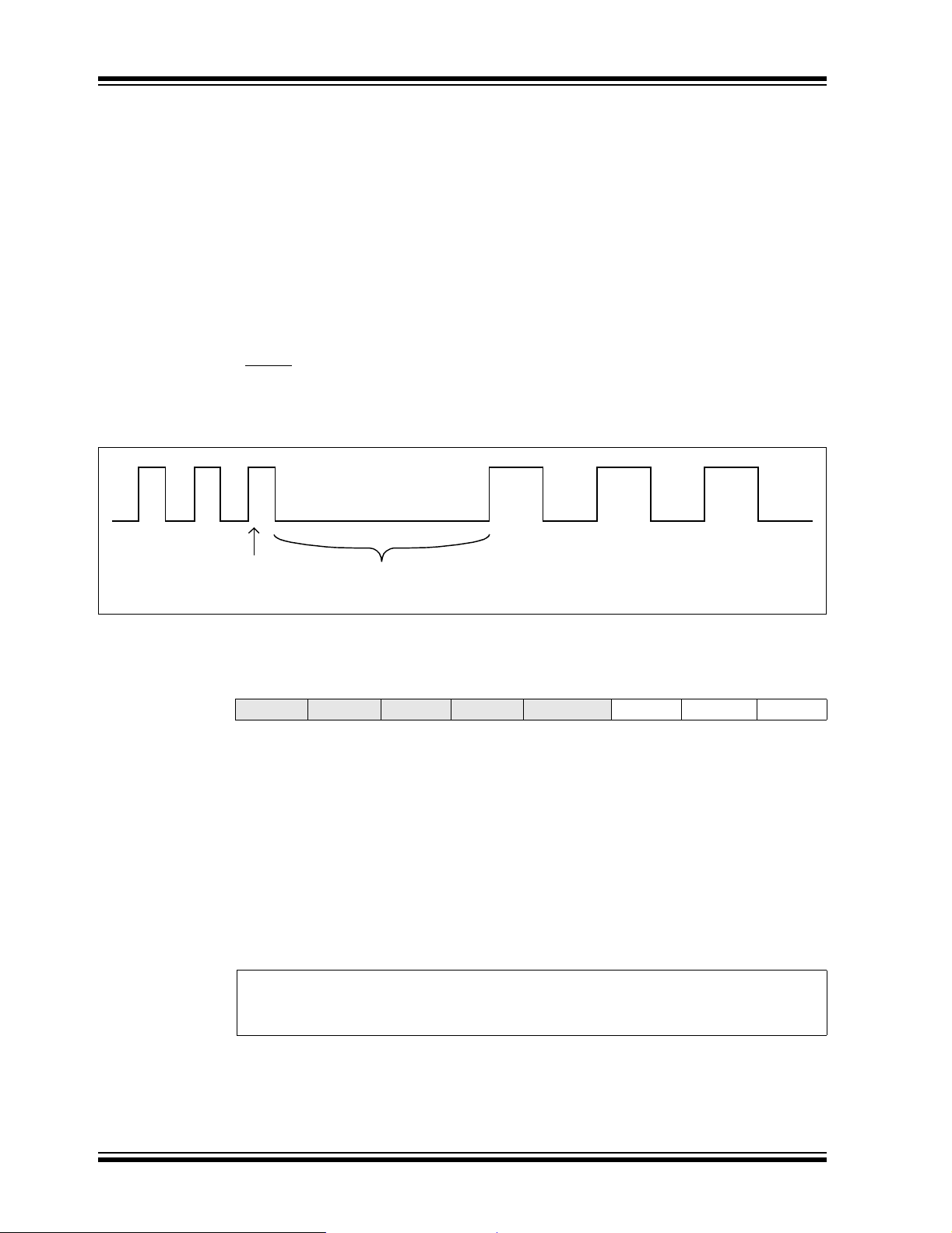
2.3 CLKOUT Pin
The clock out pin is provided to the system designer for
use as the host co ntro ller cloc k or as a c lock source for
other devices in the system. The CLKOUT has an
internal prescaler which can divide the output by 1, 2,
3, 4 or 8. The CLKOUT function is enabled and the
prescaler is selected via the ECOCON register
(Register 2-1).
To create a clean clock si gnal, the CLKOUT pin is held
low for a period when power is first applied. After the
Power-on Reset ends, the OST will begin counting.
When the OST expires , the CL KOUT pin w ill begin o utputting its default frequency of 6.25 MHz (main clock
divided by 4). At any future time that the ENC28J60 is
reset by software or the RESET
tion will not be altered (ECOCON will not change
FIGURE 2-3: CLKOUT TRANSITION
ECOCON
Changed
pin, the CLKOUT func-
80 ns to 320 ns Delay
value). Additionally, Power-Down mode may be
entered and the CLKOUT function will continue to
operate. When Power-Down mode is cancelled, the
OST will be reset but the CLKOUT function will
continue. When the CLKOUT function is disabled
(ECOCON = 0), the CLKOUT pin is driven low.
The CLKOUT function is designed to ensure that minimum timings are preserved when the CLKOUT pin
function is enabled, disabled or the prescaler value is
changed. No high or low p ulses will be outputte d whic h
exceed the frequency specified by the ECOCON
configuration. Howe ve r, when switching frequenc ies , a
delay between two and eight OSC1 clock periods will
occur where no clock pulses will be produced (see
Figure 2-3). During this period, CLKOUT will be held
low.
REGISTER 2-1: ECOCON: CLOCK OUTPUT CONTROL REGISTER
U-0 U-0 U-0 U-0 U-0 R/W-1 R/W-0 R/W-0
— — — — — COCON2 COCON1 COCON0
bit 7 bit 0
bit 7-3 Unimplemented: Read as ‘0’
bit 2-0 COCON2:COCON0: Clock Output Configuration bits
111 = Reserved for factory test. Do not use. Glitch p revention not assured.
110 = Reserved for factory test. Do not use. Glitch p revention not assured.
101 = CLKOUT outputs main clock divided by 8 (3.125 MHz)
100 = CLKOUT outputs main clock divided by 4 (6.25 MHz)
011 = CLKOUT outputs main clock divided by 3 (8.333333 MHz)
010 = CLKOUT outputs main clock divided by 2 (12.5 MHz)
001 = CLKOUT outputs main clock divided by 1 (25 MHz)
000 = CLKOUT is disabled. The pin is driven low.
Legend:
R = Readable bit W = Writable bit U = Unimplemented bit, read as ‘0’
-n = Value at POR ‘1’ = Bit is set ‘0’ = Bit is cleared x = Bit is unknown
DS39662A-page 6 Advance Information 2004 Microchip Technology Inc.
Page 9
ENC28J60
2.4 Magnetics, Termination and Other External Components
To complete the Ethernet interface, the ENC28J60
requires several standard components to be installed
externally. These component s s hou ld b e co nn ected as
shown in Figure 2-4.
On the differential receive pins (TPIN+/TPIN-), a
1:1 pulse transformer rated for 10BASE-T operation is
required. On the differential transmit pins
(TPOUT+/TPOUT-), a 1:1 pulse transformer with a
center tap is required. The transformers should be
rated for isolation of 2 kV or more to protect against
static voltages. See Secti on 16.0 “Electri c a l Ch ar ac -
teristics” for specific tr ansformer requ irements. Both
portions additional ly re qu ire two 50Ω, 1% resist ors an d
a 0.01 µF capacitor for proper termination.
The internal analog circuitry in the ENC28J60 requires
that an external 2 kΩ, 1% resistor be attached from
RBIAS to ground.
FIGURE 2-4: EXTERNAL CONNECTIONS
MCU
I/O
SCK
SDO
SDI
INT0
INT1
5.0V ← 3.3V
Level
Shift
(2)
Logic
CS
SCK
SI
SO
ENC28J60
INT
WOL
Some of the digital circuitry in the ENC28J60 operates
at a nominal 2.5V to reduce power consumption. A
2.5V regulator is in corporated int ernally to gen erate the
necessary voltage. The only external component
required is a 10 µF capacitor for stability purposes. This
capacitor should be attached from V
CAP to ground. The
internal regulator was not designed to drive external
loads.
All power supply pins must be externally connected to
the same 3.3V power source. Similarly, all ground
references should be e xternally con nected to t he same
ground node. Each V
DD and VSS pin pair should ha ve
a 0.1 µF ceramic bypass capacitor placed as close to
the pins as possible. Relatively high currents are necessary to operate the twisted p air interfa ce, so all wire s
should be kept as short as possible and reasonable
wire widths should be used on power wires to reduce
resistive loss.
TPOUT
TPOUT-
TPIN+
TPIN-
3.3V
+
50Ω
1%
50Ω
1%
50Ω
1%
50Ω
1%
Ferrite
Bead
0.01 µF
0.01 µF
(1)
1:1 CT
1:1
RJ-45
1
2
3
4
5
6
7
VCAP
LEDA
LEDB
10 µF
Note 1: Ferrite Bead should be rated for at least 100 mA.
2: Required only if the microcontroller is operating at 5V.
2004 Microchip Technology Inc. Advance Information DS39662A-page 7
RBIAS
2K
1%
8
.001 µF
2kV
Page 10
ENC28J60
2.5 I/O Levels
The ENC28J60 is a 3.3V part; however, it was
designed to be easily integrated into 5V systems. The
, SCK and SI inputs, as well as the RESET pin,
SPI CS
are all 5V tolerant. On the other hand, if the host
controller is operated at 5V, it quite likely will not be
within specifications when its SPI and interrupt inputs
are driven by the 3.3V CMOS outputs on the
ENC28J60. A unidirectiona l level translato r would be
necessary.
An economical 74H CT08 (q uad A ND ga te), 7 4ACT125
(quad 3-state buffer) or many other 5V CMOS chips
with TTL level input b uf fers may b e used t o provi de the
necessary level shifting. The use of 3-state buffers
permits easy integration into systems which share the
SPI bus with other devices. Figure 2-5 and Figure 2-6
show example translation schemes.
FIGURE 2-5: LEVEL SHIFTING USING
AND GATES
MCU
I/O
SCK
SO
SI
OSC1
ENC28J60
CS
SCK
SI
SO
CLKOUT
2.6 LED Configuration
The LEDA and LEDB pins support automatic polarity
detection on Reset. The LEDs can be connected such
that the pin must source current to turn the LED on, or
alternately connected such that the pin must sink current to turn the LED on. Upon system Reset, the
ENC28J60 will detect how the LED is connected and
begin driving the LED to the de fault st ate conf igured by
the PHLCON register. If the LED polarity is changed
while the EN C28J60 is oper ating , the n ew polar ity wi ll
not be detected until the next system Reset occurs.
LEDB is unique in that the connection of the LED is
automatically read on Reset and determi nes how to initialize the PHCON1.PDPXMD bit. If the pin sources
current to illuminate the LED, the bit is cleared on
Reset and the PHY defau lt s t o h alf -d uplex operation. If
the pin sinks curre nt to i llumi nate t he LED, the bit is set
on Reset and the PHY defaults to ful l-duplex opera tion.
Figure 2-7 shows the two available options. If no LED
is attached to the LEDB pin, the PDPXM D bit will res et
to an indeterminate value.
FIGURE 2-7: LEDB POLARITY AND
RESET CONFIGURATION
OPTIONS
+3.3VFull-Duplex Operation:
PDPXMD = 1
INT0
INT1
INT
WOL
FIGURE 2-6: LEVEL SHIFTING USING
3-STATE BUFFERS
MCU
I/O
SCK
SO
SI
OSC1
INT0
INT1
ENC28J60
CS
SCK
SI
SO
CLKOUT
INT
WOL
LEDB
Half-Duplex Operation:
PDPXMD = 0
LEDB
DS39662A-page 8 Advance Information 2004 Microchip Technology Inc.
Page 11

ENC28J60
REGISTER 2-2: PHLCON: PHY MODULE LED CONTROL REGISTER
R/W-0 R/W-0 R/W-1 R/W-1 R/W-0 R/W-1 R/W-0 R/W-0
r r r r LACFG3 LACFG2 LACFG1 LACFG0
bit 15 bit 8
R/W-0 R/W-0 R/W-1 R/W-0 R/W-0 R/W-0 R/W-1 R/W-x
LBCFG3 LBCFG2 LBCFG1 LBCFG0 LFRQ1 LFRQ0 STRCH r
bit 7 bit 0
bit 15-12 Reserved: Write as ‘0’
bit 11-8 LACFG3:LACFG0: LEDA Configuration bits
0000 = Reserved
0001 = Display transmit activity (stretchable)
0010 = Display receive activity (stretchable)
0011 = Display collision activity (stretchable)
0100 = Display link status
0101 = Display duplex status
0110 = Reserved
0111 = Display transmit and receive activity (stretchable)
1000 = On
1001 = Off
1010 = Blink fast
1011 = Blink slow
1100 = Display link status and receive activity (always stretched)
1101 = Display link status and transmit/receive activity (always stretched)
1110 = Display duplex status and collision activity (always stretched)
1111 = Reserved
bit 7-4 LBCFG3:LBCFG0: LEDB Configuration bits
0000 = Reserved
0001 = Display transmit activity (stretchable)
0010 = Display receive activity (stretchable)
0011 = Display collision activity (stretchable)
0100 = Display link status
0101 = Display duplex status
0110 = Reserved
0111 = Display transmit and receive activity (stretchable)
1000 = On
1001 = Off
1010 = Blink fast
1011 = Blink slow
1100 = Display link status and receive activity (always stretched)
1101 = Display link status and transmit/receive activity (always stretched)
1110 = Display duplex status and collision activity (always stretched)
1111 = Reserved
bit 3-2 LFRQ1:LFRQ0: LED Pulse Stretch Time Configuration bits
11 = Reserved
10 = Stretch LED events to approximately 139 ms
01 = Stretch LED events to approximately 73 ms
00 = Stretch LED events to approximately 40 ms
bit 1 STRCH: LED Pulse Stretching Enable bit
1 = Stretchable LED events will cause lengthened LED pulses based on the LFRQ configuration
0 = Stretchable LED events will only be displayed while they are occurring
bit 0 Reserved: Write as ‘0’
Legend:
R = Readable bit W = Writable bit r = Reserved bit
-n = Value at POR ‘1’ = Bit is set ‘0’ = Bit is cleared x = Bit is unknown
2004 Microchip Technology Inc. Advance Information DS39662A-page 9
Page 12

ENC28J60
NOTES:
DS39662A-page 10 Advance Information 2004 Microchip Technology Inc.
Page 13

ENC28J60
3.0 MEMORY ORGANIZATION
The Ethernet buffer contains transmit and receive
memory used by the Ethernet controller in a single
All memory in the ENC2 8J60 is im ple mente d as s tatic
RAM. There are three types of memory in the
ENC28J60:
• Control Registers
• Ethernet Buffer
• PHY Registers
The control registers’ memory contains Control
Registers (CRs). These are used for configuration,
control and status retrieval of the ENC28J60. The
Control Registers are directly read and written to by the
SPI interface.
memory space. The sizes of the memory areas are
programmable by the host controller using the SPI
interface. The Ethernet buffer memory can only be
accessed via the read buffer memory and write buffer
memory SPI commands (see Section 4.2.2 “Read
Buffer Memory Command” and Section 4.2.4 “Write
Buffer Memory Command”).
The PHY registers are used for con figuration, c ontrol and
status retriev al of th e PHY mod ule. T he regi ster s are no t
directly accessible through the SPI interface; they can
only be accessed through the Media Independent
Interface (MII) implemented in the MAC.
Figure 3-1 shows the dat a memory org anizatio n for the
ENC28J60.
FIGURE 3-1: ENC28J60 MEMORY ORGANIZATION
ECON1<1:0>
= 00
Bank 0
Control Registers
00h
19h
1Ah
1Fh
00h
Common
Registers
Buffer Pointers in Bank 0
Ethernet Buffer
0000h
= 01
= 10
= 11
Note: Memory areas are not shown to scale. The size of the control memory space has been scaled to show detail.
Bank 1
Bank 2
Bank 3
19h
1Ah
1Fh
00h
19h
1Ah
1Fh
00h
19h
1Ah
1Fh
Common
Registers
Common
Registers
Common
Registers
1FFFh
PHY Registers
00h
1Fh
2004 Microchip Technology Inc. Advance Information DS39662A-page 11
Page 14

ENC28J60
3.1 Control Registers
Some of the available addresses are unimplemented.
Any attempts to write to these locations are ignored
The Control Registers provide the main interface
between the ho st controller and the on -chip Ethernet
controller logic. Writing to these registers controls the
operation of the interface, while reading t he registers
allows the host controller to monitor operations.
The Control Register memory is partitioned into four
banks, selectable by the bank select bits
BSEL1:BSEL0 in the ECON1 register. Each bank is
32 bytes long and add resse d by a 5-bit addres s va lue.
The last five locations (1Bh to 1Fh) of all banks point to a
common set of registers: EIE, EIR, ESTAT, ECON2 and
ECON1. These are key register s used in controll ing and
monitoring t he operation of the device. Their common
while reads return ‘0’s. The register at address 1Ah in
each bank is reserved; read and write operations
should not be performed on this register. All other
reserved registers ma y be read, but their content s must
not be changed. When reading and writing to registers
which contain reserved bits, any rules stated in the
register definition shou ld be observ ed.
Control registers for the ENC28J60 are generically
grouped as ETH, MAC and MII registers. Register
names starting with “E” belong to the ETH group.
Similarly, registers names starting with “MA” belong to
the MAC group and registers prefixed with “MI” belong
to the MII group.
mapping allows easy access without switching the bank.
The ECON1 and ECON2 registers are discussed later in
this section.
TABLE 3-1: ENC28J60 CONTROL REGISTER MAP
Bank 0 Bank 1 Bank 2 Bank 3
Address Name Address Name Address Name Address Name
00h ERDPTL 00h EHT0 00h MACON1 00h MAADR1
01h ERDPTH 01h EHT 1 01h MACON2 01h M AADR0
02h EWRPTL 02h EHT2 02h M ACO N3 02h MAADR3
03h EWRPTH 03h EHT3 03h MACON4 03h MAADR2
04h ETXSTL 04h EHT4 04h MABBIPG 04h MAADR5
05h ETXSTH 05h EHT5 05h
06h ETXNDL 06h EHT6 06h MAIPGL 06h EBSTSD
07h ETXNDH 07h EHT7 07h MAIPGH 07h EBSTCON
08h ERXSTL 08h EPMM0 08h MACLCON1 08h EBSTCSL
09h ERXSTH 09h EPMM1 09h MACLCON2 09h EBSTCSH
0Ah ERXNDL 0Ah EPMM2 0Ah MAMXFLL 0Ah MISTAT
0Bh ERXNDH 0Bh EPMM3 0Bh MAMXFLH 0Bh
0Ch ERXRDPTL 0Ch EPMM4 0Ch Reserved 0Ch
0Dh ERXRDPTH 0Dh EPMM5 0Dh MAPHSUP 0Dh
0Eh ERXW R PTL 0Eh EPMM6 0Eh Reserved 0Eh
0Fh ERXWRPTH 0Fh EPMM7 0Fh
10h EDMASTL 10h EPMCSL 10h Reserved 10h
11h EDMASTH 11h EPMCSH 11h MICON 11h
12h EDMANDL 12h
13h EDMANDH 13h
14h EDMADSTL 14h EPMOL 14h MIREGADR 14h
15h EDMADSTH 15h EPMOH 15h Reserved 15h ECOCON
16h EDMACSL 16h EWOLIE 16h MIWRL 16h Reserved
17h EDMACSH 17h EWOLIR 17h MIWRH 17h EFLOCON
18h
19h
1Ah Reserved 1Ah Rese rved 1Ah Reserved 1Ah Reserved
1Bh EIE 1Bh EIE 1Bh EIE 1Bh EIE
1Ch EIR 1Ch EIR 1Ch EIR 1Ch EIR
1Dh ESTAT 1Dh ESTAT 1Dh ESTAT 1Dh ESTAT
1Eh ECON2 1Eh ECON2 1Eh ECON2 1Eh ECON2
1Fh ECON1 1Fh ECON1 1Fh ECON1 1Fh ECON1
— 18h ERXFCON 18h MIRDL 18h EPAUSL
— 19h EPKTCNT 19h MIRDH 19h EPAUSH
— 12h MICMD 12h EREVID
— 13h — 13h —
— 05h MAADR4
—0Fh—
—
—
—
—
—
—
—
DS39662A-page 12 Advance Information 2004 Microchip Technology Inc.
Page 15

ENC28J60
TABLE 3-2: ENC28J60 CONTROL REGISTER SUMMARY
Register Name Bit 7 Bit 6 Bit 5 Bit 4 Bit 3 Bit 2 Bit 1 Bit 0
EIE INTIE PKTIE DMAIE LINKIE TXIE WOLIE TXERIE RXERIE 0000 0000 67
EIR
ESTAT INT r r LATECOL
ECON2 AUTOINC PKTDEC PWRSV
ECON1 TXRST RXRST DMAST CSUMEN TXRTS RXEN BSEL1 BSEL0 0000 0000 15
ERDPTL Read Pointer Low Byte ERDPT<7:0>) 1111 1010 17
ERDPTH
EWRPTL Write Pointer Low Byte (EWRPT<7:0>) 0000 0000 17
EWRPTH
ETXSTL TX Sta rt Low Byte (ETXST<7:0>) 0000 0000 17
ETXSTH
ETXNDL TX End Low Byte (ETXND<7:0>) 0000 0000 17
ETXNDH
ERXSTL RX Start Low Byte (ERXST<7:0>) 1111 1010 17
ERXSTH
ERXNDL RX End Low Byte (ERXND<7:0>) 1111 1111 17
ERXNDH
ERXRDPTL RX RD Pointer Low Byte (ERXRDPT<7:0>) 1111 1010 17
ERXRDPTH
ERXWRPTL RX WR Pointer Low Byte (ERXWRPT<7:0>) 0000 0000 17
ERXWRPTH
EDMASTL DMA Start Low Byte (EDMAST<7:0>) 0000 0000 75
EDMASTH
EDMANDL DMA End Low Byte (EDMAND<7:0>) 0000 0000 75
EDMANDH
EDMADSTL DMA Destination Low Byte (EDMADST<7:0>) 0000 0000 75
EDMADSTH
EDMACSL DMA Checksum Low Byte (EDMACS<7:0>) 0000 0000 76
EDMACSH DMA Checksum High Byte (EDMACS<15:8> ) 0000 0000 76
EHT0 Hash Table Byte 0 (EHT<7:0>) 0000 0000 52
EHT1 Hash Table Byte 1 (EHT<15:8>) 0000 0000 52
EHT2 Hash Table Byte 2 (EHT<23:16>) 0000 0000 52
EHT3 Hash Table Byte 3 (EHT<31:24>) 0000 0000 52
EHT4 Hash Table Byte 4 (EHT<39:32>) 0000 0000 52
EHT5 Hash Table Byte 5 (EHT<47:40>) 0000 0000 52
EHT6 Hash Table Byte 6 (EHT<55:48>) 0000 0000 52
EHT7 Hash Table Byte 7 (EHT<63:56>) 0000 0000 52
EPMM0 Pattern Match Mask Byte 0 (EPMM<7:0>) 0000 0000 51
EPMM1 Pattern Match Mask Byte 1 (EPMM<15:8>) 0000 0000 51
EPMM2 Pattern Match Mask Byte 2 (EPMM<23:16>) 0000 0000 51
EPMM3 Pattern Match Mask Byte 3 (EPMM<31:24>) 0000 0000 51
EPMM4 Pattern Match Mask Byte 4 (EPMM<39:32>) 0000 0000 51
EPMM5 Pattern Match Mask Byte 5 (EPMM<47:40>) 0000 0000 51
EPMM6 Pattern Match Mask Byte 6 (EPMM<55:48>) 0000 0000 51
EPMM7 Pattern Match Mask Byte 7 (EPMM<63:56>) 0000 0000 51
EPMCSL Pattern Match Checksum Low Byte (EPMCS<7:0>) 0000 0000 51
EPMCSH Pattern Match Checksum High Byte (EPMCS<15:0>) 0000 0000 51
Legend: x = unknown , u = unchanged, — = unimplemented, q = value depends on condition, r = reserved, do not modify.
Note 1: CLKRDY resets to ‘0’ on Power-on Reset but is unaffected on all other Resets.
2: EREVID is a read-only register.
3: ECOCON resets to ‘---- -100’ on Power-on Reset and ‘---- -uuu’ on all other Resets.
— PKTIF DMAIF LINKIF TXIF WOLIF TXERIF RXERIF -000 0000 68
— RXBUSY TXABRT CLKRDY
—VRPS — — — 100- 0--- 16
— — — Read Pointer High Byt e (ER DPT<12 :8>) ---0 0101 17
— — — Write Pointer High Byte (EWRPT<12:8>) ---0 0000 17
— — — TX Start High Byte (ETXST<12:8>) ---0 0000 17
— — — TX End High Byte (ETXND<12:8>) ---0 0000 17
— — — RX Start High Byte (ERXST<12:8>) ---0 0101 17
— — — RX End High Byte (ERXND<12:8>) ---1 1111 17
— — — RX RD Pointer High Byte (ERXRDPT<12:8>) ---0 0101 17
— — — RX WR Pointer High Byte (ERXWRPT<12:8>) ---0 0000 17
— — — DMA Start High Byte (EDMAST<12:8>) ---0 0000 75
— — — DMA End High Byte (EDMAND<12:8>) ---0 0000 75
— — — DMA Destination High Byte (EDMADST<12:8>) ---0 0000 75
Value
Reset
(1)
0000 -000 66
Details
on
on
Page
2004 Microchip Technology Inc. Advance Information DS39662A-page 13
Page 16

ENC28J60
TABLE 3-2: ENC28J60 CONTROL REGISTER SUMMARY (CONTINUED)
Register Name Bit 7 Bit 6 Bit 5 Bit 4 Bit 3 Bit 2 Bit 1 Bit 0
EPMOL Pattern Match Offset Low Byte (EPMO<7:0>) 0000 0000 51
EPMOH
EWOLIE UCWOLIE AWOLIE
EWOLIR UCWOLIF AWOLIF
ERXFCON UCEN ANDOR CRCEN PMEN MPEN HTEN MCEN BCEN 1010 0001 48
EPKTCNT Ethernet Packet Count 0000 0000 43
MACON1
MACON2 MARST RNDRST
MACON3 PADCFG2 PADCFG1 PADCFG0 TXCRCEN PHDRLEN HFRMEN FRMLNEN FULDPX 0000 0000 35
MACON4
MABBIPG
MAIPGL
MAIPGH
MACLCON1
MACLCON2
MAMXFLL Maximum Frame Length Low Byte (MAMXFL<7:0>) 0000 0000 34
MAMXFLH Maximum Frame Length High Byte (MAMXFL<15:8>) 0000 0110 34
MAPHSUP RSTINTFC
MICON RSTMII
MICMD
MIREGADR
MIWRL MII Write Data Low Byte (MIWR<7:0>) 0000 0000 19
MIWRH MII Write Data High Byte (MIWR<15:8>) 0000 0000 19
MIRDL MII Read Data Low Byte (MIRD<7:0>) 0000 0000 19
MIRDH MII Read Data High Byte(MIRD<15:8>) 0000 0000 19
MAADR1 MAC Address Byte 1 (MAADR<15:8>) 0000 0000 34
MAADR0 MAC Address Byte 0 (MAADR<7:0>) 0000 0000 34
MAADR3 MAC Address Byte 3 (MAADR<31:24>) 0000 0000 34
MAADR2 MAC Address Byte 2(MAADR<23:16>) 0000 0000 34
MAADR5 MAC Address Byte 5 (MAADR<48:41>) 0000 0000 34
MAADR4 MAC Address Byte 4 (MAADR<40:32>) 0000 0000 34
EBSTSD Built-in Self-Test Fill Seed (EBSTSD<7:0>) 0000 0000 80
EBSTCON PSV2 PSV1 PSV0 PSEL TMSEL1 TMSEL0 TME BISTST 0000 0000 79
EBSTCSL Built-in Self-Test Checksum Low Byte (EBSTCS<7:0>) 0000 0000 80
EBSTCSH Built-in Self-Test Checksum High Byte (EBSTCS<15:8>) 0000 0000 80
MISTAT
(2)
EREVID
ECOCON
EFLOCON
EPAUSL Pause Timer Value Low Byte (EPAUS<7:0>) 0000 0000 57
EPAUSH Pause Timer Value High Byte (EPAUS<15:8>) 0001 0000 57
Legend: x = unknown , u = unchanged, — = unimplemented, q = value depends on condition, r = reserved, do not modify.
Note 1: CLKRDY resets to ‘0’ on Power-on Reset but is unaffected on all other Resets.
(3)
2: EREVID is a read-only register.
3: ECOCON resets to ‘---- -100’ on Power-on Reset and ‘---- -uuu’ on all other Resets.
— — — Pattern Match Offset High Byte (EPMO<12:8>) ---0 0000 51
— PMWOLIE MPWOLIE HTWOLIE MCWOLIE BCWOLIE 00-0 0000 72
— PMWOLIF MPWOLIF HTWOLIF MCWOLIF BCWOLIF 00-0 0000 73
— — — LOOPBK TXPAUS RXPAUS PASSALL MARXEN ---0 0000 34
— — MARXRST RFUNRST MATXRST TFUNRST 10-- 0000 61
— DEFER BPEN NOBKOFF — — LONGPRE PUREPRE -000 --00 36
— Back-to-Back Inter-Packet Gap (BBIPG<6:0>) -000 0000 37
— Non-Back-to-Back Inter-Packet Gap Low Byte (MAIPGL<6:0>) -000 0000 34
— Non-Back-to-Back Inter-Packet Gap High Byte (MAIPGH<6:0>) -000 0000 34
— — — — Retransmission Maximum (RETMAX<3:0>) ---- 1111 34
— — Collision Window (COLWIN<5:0>) --11 0111 34
— —rRSTRMII— —r0--1 0--0 62
— — — — — — — 0--- ---- 21
— — — — — — MIISCAN MIIRD ---- --00 21
— — — MII Register Address (MI REG AD R<4:0 > ) ---0 0000 19
— — — — r NVALID SCAN BUSY ---- 0000 22
— — — Ethernet Revision ID (EREVID<4:0>) ---q qqqq 22
— — — — — COCON2 COCON1 COCON0 ---- -100 6
— — — — — FULDPXS FCEN1 FCEN0 ---- -000 56
Value
Reset
Details
on
on
Page
DS39662A-page 14 Advance Information 2004 Microchip Technology Inc.
Page 17

3.1.1 ECON1 REGISTER
The ECON1 register, shown in Register 3-1, is used to
control the main functions of the ENC28J60. Receive
enable, transmit request, DMA control and bank select
bits can all be found in ECON1.
REGISTER 3-1: ECON1: ETHERNET CONTROL REGISTER 1
R/W-0 R/W-0 R/W-0 R/W-0 R/W-0 R/W-0 R/W-0 R/W-0
TXRST RXRST DMAST CSUMEN TXRTS RXEN BSEL1 BSEL0
bit 7 bit 0
bit 7 TXRST: Transmit Logic Reset bit
1 = Transmit logic is held in Reset
0 = Normal operation
bit 6 RXRST: Receive Logic Reset bit
1 = Receive logic is held in Reset
0 = Normal operation
bit 5 DMAST: DMA Start and Busy Status bit
1 = DMA copy or checksum operation is in progress
0 = DMA hardware is Idle
bit 4 CSUMEN: DMA Checksum Enable bit
1 = DMA hardware calculates checksums
0 = DMA hardware copies buffer memory
bit 3 TXRTS: Transmit Request To Send bit
1 = The transmit logic is attempting to transmit a packet
0 = The transmit logic is Idle
bit 2 RXEN: Receive Enable bit
1 = Packets which pass the current filter configuration will be written into the receive buffer
0 = All packets received will be ignored
bit 1-0 BSEL1:BSEL0: Bank Select bit s
11 = SPI accesses registers in Bank 3
10 = SPI accesses registers in Bank 2
01 = SPI accesses registers in Bank 1
00 = SPI accesses registers in Bank 0
ENC28J60
Legend:
R = Readable bit W = Writable bit U = Unimplemented bit, read as ‘0’
-n = Value at POR ‘1’ = Bit is set ‘0’ = Bit is cleared x = Bit is unknown
2004 Microchip Technology Inc. Advance Information DS39662A-page 15
Page 18

ENC28J60
3.1.2 ECON2 REGISTER
The ECON2 register, shown in Register 3-2, is used to
control other main functions of the ENC28J60.
REGISTER 3-2: ECON2: ETHERNET CONTROL REGISTER 2
R/W-1 W-0 R/W-0 U-0 R/W-0 U-0 U-0 U-0
AUTOINC PKTDEC PWRSV
bit 7 bit 0
bit 7 AUTOINC: Automatic Buffer Pointer Increment Enable bit
1 = Automatically increment ERDP T and EW RP T when th e SPI RBM/W BM c ommand i s used
0 = Do not automatically change ERDPT and EWRPT after the buffer is accessed
bit 6 PKTDEC: Packet Decrement bit
1 = Decrement the EPKTCNT register by one
0 = Leave EPKTCNT unchanged
bit 5 PWRSV: Power Save Enable bit
1 = MAC, PHY and control logic are in Low-Power Sleep mode
0 = Normal operation
bit 4 Unimplemented: Read as ‘0’
bit 3 VRPS: Voltage Regulator Power Save Enable bit
When PWRSV =
1 = Internal voltage regulator is in Low-Current mode
0 = Internal voltage regulator is in Normal Current mode
When PWRSV = 0:
The bit is ignored; the regulator always outputs as much current as the device requires.
bit 2-0 Unimplemented: Read as ‘0’
1:
—VRPS— — —
Legend:
R = Readable bit W = Writable bit U = Unimplemented bit, read as ‘0’
- n = Value at POR ‘1’ = Bit is set ‘0’ = Bit is cleared x = Bit is unknown
DS39662A-page 16 Advance Information 2004 Microchip Technology Inc.
Page 19

ENC28J60
3.2 Ethernet Buffer
The Ethernet buffer contains transmit and receive
memory used by the Ethernet controller. The entire
buffer is 8 Kbytes, divided into separate receive and
transmit buffer spaces. The sizes and locations of
transmit and receive memory are fully programmable
by the host controller using the SPI interface.
The relationship of the buffer spaces is shown in
Figure 3-2.
3.2.1 RECEIVE BUFFER
The receive buffer constitutes a circular FIFO buffer
managed by hardware. The register pairs
ERXSTH:ERXSTL and ERXNDH:ERXNDL serve as
pointers to define the buffer’s size and location within
the memory. The byte pointed to by ERXST and the
byte pointed to by ERXND are both included in the
FIFO buffer.
As bytes of data are received from the Ethernet
interface, they are written into the receive buffer
sequentially. However, after the memory pointed to by
ERXND is written to, the hardware will automatically
write the next byte of received data to the memory
pointed to by ERXST. As a re sult, the r eceive hardwa re
will never write outside the boundaries of the FIFO.
The host controller may program the ERXST and
ERXND pointers when the rec eive logic is no t enable d.
The pointer s must not be modified w hile the receive
logic is enabled (ECON1.RXEN is set). If desired, the
pointers may span the 1FFFh to 0000h memory
boundary; the hardware will still operate as a FIFO.
The ERXWRPTH:ERXWRPTL registers define a
location within the FIFO where the hardware will write
bytes that it receives. The pointer is read-only and is
automatically updated by the hardware whenever a
new packet is successfully received. The pointer is
useful for determining how much free space is
available within the FIFO.
The ERXRDPT registers define a location within the
FIFO where the receive hardware is forbidden to write
to. In normal operation, the receive hardware will write
data up to, but not inc lu din g, the me mory pointed to by
ERXRDPT. If the FIFO fills up with data and new data
continues to arrive, the hardware will not overwrite the
previously received data. Instead, the new data will be
thrown away and the old data will be preserved. In
order to continuously receive new data, the host controller must periodicall y adv an ce this poin ter w hen ev er
it finishes processing some, or all, of the old received
data.
3.2.2 TRANSMIT BU FFER
Any space within the 8-Kbyte memory, which is not
programmed as part of the receive FIFO buffer, is
considered to be the transmit buffer. The responsibility
of managing where packets are located in the transmit
buffer belongs to the host contro ller . Whenever the hos t
controller decides to t rans mit a p ack et, the ETXST an d
ETXND pointers are programmed with addresses
specifying where, within the transmit buffer, the particular packet to transmit is located. The hardware does
not check that the start and end addresses do not
overlap with the receive buffer. To prevent buffer
corruption, the host contr oller must make sure to not
transmit a packet while the ETXST and ETXND
pointers are overlappin g the recei ve buf fer , or w hile the
ETXND pointer is too close to the receive buffer. See
Section 7.1 “Transmitting Packets” for more
information.
3.2.3 READING AND WRITING TO THE BUFFER
The Ethernet buffer contents are accessed from the
host controller though separate read and write pointers
(ERDPT and EWRPT) combined with the read buffer
memory and write buffer memory SPI commands.
While sequentially reading from the receive buffer, a
wrapping condition will occur at the end of the receive
buffer. While sequentially wri ting to the bu ff er, no wrapping conditions will occur. See Section 4.2.2 “Read
Buffer Memory Command” and Section 4.2.4 “Write
Buffer Memory Command” for more information.
3.2.4 DMA ACCESS TO THE BUFFER
The integrated DMA controller must read from the buffer
when calculating a checksum and it must read and write
to the buffer when copying memory. The DMA follows
the same wrapping rules that SPI accesses do. While it
sequentially reads, it will be subject to a w rapping condition at the end of the receive buffer . All w rites it does w ill
not be subject to any wrapping conditions. See
Section 13.0 “Direct Memory Access Controller” for
more information.
2004 Microchip Technology Inc. Advance Information DS39662A-page 17
Page 20
ENC28J60
FIGURE 3-2: ETHERNET BUFFER ORGANIZATION
Transmit Buffer Start
(ETXSTH:ETXSTL)
Buffer Write Pointer
(EWRPTH:EWRPTL)
Transmit Buffer End
(ETXNDH:ETXNDL)
Receive Buffer Start
(ERXSTH:ERXSTL)
Buffer Read Pointer
(ERDPTH:ERDPTL)
AAh
Transmit
Buffer
Receive
Buffer
(Circular FIFO)
55h
0000h
Transmit Buffer Data
(WBM AAh)
Receive Buffer Data
(RBM 55h)
Receive Buffer End
(ERXNDH:ERXNDL)
DS39662A-page 18 Advance Information 2004 Microchip Technology Inc.
1FFFh
Page 21

ENC28J60
3.3 PHY Registers
The PHY registers provide con fig uration and control of
the PHY module, as well as stat us inform ation ab out it s
operation. All PHY registers are 16 bits in width. There
are a total of 32 PHY addres se s; ho wev er, only 9 locations are implemented. Writes to unimplemented
locations are ignored and any attempts to read the se
locations will return ‘0’. All reserved locations shoul d be
written as ‘0’; their contents should be ignored when
read.
Unlike the ETH, MAC and MII control registers, or the
buffer memory, the PHY registers are not directly
accessible through the SPI control interface. Instead,
access is accomplished through a special set of MAC
control registers that implement a Media Independent
Interface for Management (MIIM). These control registers are referred to as the MII registers. The registers
that control access to the PHY registers are shown in
Register 3-3 and Register 3-4.
3.3.1 READING PHY REGISTERS
When a PHY register is read, the entire 16 bits are
obtained.
To read from a PHY register:
1. Write the address of the PHY register to read
from into the MIREGADR register.
2. Set the MICMD.MIIRD bit. The read operation
begins and the MISTAT.BUSY bit is set.
3. Wait 10.24 µs. Poll the MISTAT.BUSY bit to be
certain that the operation is complete. While
busy, the host controller should not start any
MIISCAN operations or write to the MIWRH
register.
When the MAC has obtained the register
contents, the BUSY bit will clear itself.
4. Clear the MICMD.MIIRD bit.
5. Read the desired data from the MIRDL and
MIRDH registers. The order that these bytes are
accessed is unimportant.
3.3.2 WRITING PHY REGISTERS
When a PHY regi ster is w ritte n to, the en tire 16 bits is
written at once; selective bit writes are not implemented. If it is necessary to reprogram only select bits
in the register, the controller must first read the PHY
register, modify the resulting data and then write the
data back to the PHY register.
To write to a PHY register:
1. Write the address of the PHY register to write to
into the MIREGADR register.
2. Write the lower 8 bits of data to write into the
MIWRL register.
3. Write the upper 8 bits of data to write into the
MIWRH register. Writing to this register automatically begins the MII transaction, so it must
be written to after MIWRL. The MISTAT.BUSY
bit becomes set.
The PHY register will be written after the MII operation
completes, which takes 10.24 µs. When the write
operation has completed, the BUSY bit will clear itself.
The host controller should not start any MIISCAN or
MIIRD operations while busy.
3.3.3 SCANNING A PHY REGISTER
The MAC can be configured to perform automatic
back-to-back read operations on a PHY register. This
can significantly reduce the host controller complexity
when periodic status information updates are desired.
To perform the scan operation:
1. Write the address of the PHY register to read
from into the MIREGADR register.
2. Set the MICMD.MIISCAN bit. The scan operation begins and the MISTA T.BUSY bit is set . The
first read operation will complete after 10.24 µs.
Subsequent reads will be done at the same
interval until the operation is cancelled. The
MISTAT.NVALID bit may be polled to determine
when the first read operation is complete.
After setting the MIISCAN bit, the MIRDL and MIRDH
registers will automatically be updated every 10.24 µs.
There is no status information which can be used to
determine when the MIR D registers are updated. Since
the host controller can only read one MII register at a
time through the SPI, it must not be assumed that the
values of MIRDL and MIRDH were read from the PHY
at exactly the same time.
When the MIISCAN operation is in progress, the host
controller must not attempt to write to MIWRH or start
an MIIRD operation. The MIISCAN operation can be
cancelled by clearing the MICMD.MIISCAN bit and
then polling the MISTAT.BUSY bit. New operations may
be started after the BUSY bit is cleared.
2004 Microchip Technology Inc. Advance Information DS39662A-page 19
Page 22

ENC28J60
r — — — — — — — 00-- 10-q 0--- ----
(1)
— —PPWRSV r —PDPXMD
— — — PFDPX PHDPX — — — — — — — — LLSTAT JBSTAT — ---1 1--- ---- -00-
— FRCLNK TXDIS r r JABBER r HDLDIS r r r r r r r r -000 0000 0000 0000
— — — —PLRITY— — — — --00 00q- ---0 ----
(1)
— — TXSTAT RXSTAT COLSTAT LSTAT DPXSTAT
Addr Name Bit 15 Bit 14 Bit 13 Bit 12 Bit 11 Bit 10 Bit 9 Bit 8 Bit 7 Bit 6 Bit 5 Bit 4 Bit 3 Bit 2 Bit 1 Bit 0 Reset Values
00h PHCON1 PRST PLOOPBK
01h PHSTAT1
02h PHID1 PHY Identifier (PID18:PID3) = 0083h 0000 0000 1000 0011
03h PHID2 PHY Identifier (PID24:PID19) = 000101 PHY P/N (PPN5:PPN0) = 00h PHY Revision (PREV3:PREV0 ) = 0 0h 0001 0100 0000 0000
10h PHCON2
12h PHIE r r r r r r r r r r r PLNKIE r r PGEIE r 0000 0000 0000 0000
13h PHIR r r r r r r r r r r r PLNKIF r PGIF r r xxxx xxxx xx00 00x0
14h PHLCON r r r r LACFG3:LACFG0 LBCFG3:LBCFG0 LFRQ1:LFRQ0 STRCH r 0011 0100 0010 001x
TABLE 3-3: ENC28J60 PHY REGISTER SUMMARY
11h PHSTAT2
Legend: x = unknown, u = unchanged, — = unimplemented, q = value depends on condition, r = reserved, do not modify.
Note 1: Reset values of the Duplex mode/status bits depend on the connection of the LED to the LEDB pin (see Section 2.6 “LED Configuration” for additional details).
DS39662A-page 20 Advance Information 2004 Microchip Technology Inc.
Page 23

REGISTER 3-3: MICON: MII CONTROL REGISTER
R/W-0 U-0 U-0 U-0 U-0 U-0 U-0 U-0
RSTMII — — — — — — —
bit 7 bit 0
bit 7 RSTMII: MII Management Module Reset bit
1 = MII management module held in Reset
0 = Normal operation
bit 6-0 Unimplemented: Read as ‘0’
Legend:
R = Readable bit W = Writable bit U = Unimplemented bit, read as ‘0’
-n = Value at POR ‘1’ = Bit is set ‘0’ = Bit is cleared x = Bit is unknown
REGISTER 3-4: MICMD: MII COMMAND REGISTER
U-0 U-0 U-0 U-0 U-0 U-0 R/W-0 R/W-0
— — — — — — MIISCAN MIIRD
bit 7 bit 0
ENC28J60
bit 7-2 Unimplemented: Read as ‘0’
bit 1 MIISCAN: MII Scan Enable bit
1 = PHY register at MIREGADR is continously read and the data is placed in MIRD
0 = No MII management scan operation is in progress
bit 0 MIIRD: MII Read Enable bit
1 = PHY register at MIREGADR is read once and the data is placed in MIRD
0 = No MII management read operation is in progress
Legend:
R = Readable bit W = Writable bit U = Unimplemented bit, read as ‘0’
-n = Value at POR ‘1’ = Bit is set ‘0’ = Bit is cleared x = Bit is unknown
2004 Microchip Technology Inc. Advance Information DS39662A-page 21
Page 24

ENC28J60
REGISTER 3-5: MISTAT: MII STATUS REGISTER
U-0 U-0 U-0 U-0 R-0 R-0 R-0 R-0
— — — — r NVALID SCAN BUSY
bit 7 bit 0
bit 7-4 Unimplemented: Read as ‘0’
bit 3 Reserved: Maintain ‘0’
bit 1 NVALID: MII Management Read Data Not Valid bit
1 = The contents of MIRD are not valid yet
0 = The MII management read cycle has completed and MIRD has been updated
bit 1 SCAN: MII Management Scan Operation bit
1 = MII management scan operation is in progress
0 = No MII management scan operation is in progress
bit 0 BUSY: MII Management Busy bit
1 = A PHY register is currently being read or written to
0 = The MII management interface is Idle
Legend:
R = Readable bit r = reserved, maintain as ‘0’ U = Unimplemented bit, read as ‘0’
-n = Value at POR ‘1’ = Bit is set ‘0’ = Bit is cleared x = Bit is unknown
3.3.4 PHSTAT REGISTERS
The PHSTAT1 and PHSTAT2 registers contain readonly bits that show the current status of the PHY
module’s operations, particularly the conditions of the
communications link to the rest of the network.
The PHSTAT1 register (Register 3-6) contains the
LLSTAT bit; it clears and latches low if the physical
layer link has gone down since the last read of the
register. Periodic polling by the host controller can be
used to determine exactly when the link fails. It may be
particularly useful if the link change interrupt is not
used.
The PHST AT1 register also contai ns a jabbe r status bit.
An Ethernet controller is sa id to be “j abb erin g” if it continuously transmits data without stopping and allowing
other nodes to share the medium. G enerally, the jabber
condition indicates that the local controller may be
grossly violating the maximum packet size defined by
the IEEE specification. This bit latches high to indicate
that a jabber con dition has occurr ed sin ce th e las t read
of the register.
The PHSTAT2 register (Register 3-7) contains status
bits which report if the PHY module is linked to the
network and whether or not it is transmitting or
receiving.
3.3.5 PHID1 AND PHID2 REGISTERS
The PHID1 and PHID2 registers are read-only
registers. They hold cons tan t dat a th at help iden tify th e
Ethernet controller and may be useful for debugging
purposes. This includes:
• The part number of the PHY module
(PPN5:PPN0)
• The revision level of the PHY module
(PREV3:PREV0); and
• The PHY Identifier, as part of Microchip’s
corporate Organizati onally Uni que Identi fier (OUI)
(PID24:PID3)
The PHY part number and revision are part of PHID2.
The upper two bytes of the PHY id entifier are loca ted in
PHID1, with the remainder in PHID2. The exact
locations within registers are shown in Table 3-3.
Revision inform ation is also st ored in EREVID. Th is is
a read-only control register which contains a 5-bit
identifier for the specific silicon revision level of the
device. Details of this register are shown in Table3-2.
DS39662A-page 22 Advance Information 2004 Microchip Technology Inc.
Page 25

ENC28J60
REGISTER 3-6: PHSTAT1: PHYSICAL LAYER STATUS REGISTER 1
U-0 U-0 U-0 R-1 R-1 U-0 U-0 U-0
— — — PFDPX PHDPX — — —
bit 15 bit 8
U-0 U-0 U-0 U-0 U-0 R/LL-0 R/LH-0 U-0
— — — — — LLSTAT JBRSTAT —
bit 7 bit 0
bit 15-13 Unimplemented: Read as ‘0’
bit 12 PFDPX: PHY Full-Duplex Capable bit
1 = PHY is capable of operating at 10 Mbps in Full-Duplex mode (this bit is always set)
bit 11 PHDPX: PHY Half-Duplex Capable bit
1 = PHY is capable of operating at 10 Mbps in Half-Duplex mode (this bit is always set)
bit 10-3 Unimplemented: Read as ‘0’
bit 2 LLSTAT: PHY Latching Link Status bit
1 = Link is up and has been up continously since PHSTAT1 was last read
0 = Link is down or was down for a period since PHSTAT1 was last read
bit 1 JBRSTAT: PHY Latching Jabber Status bit
1 = PHY has detected a transmission meeting the jabber criteria since PHYSTAT1 was last read
0 = PHY has not detected any jabbering transmissions since PHYSTAT1 was last read
bit 0 Unimplemented: Read as ‘0’
Legend:
R = Read-only bit R/L = Read-only latch bit U = Unimplemented bit, read as ‘0’
‘1’ = Bit is set on POR ‘0’ = Bit is cleared on POR L L = Bit latches low LH = Bit latches high
2004 Microchip Technology Inc. Advance Information DS39662A-page 23
Page 26

ENC28J60
REGISTER 3-7: PHSTAT2: PHYSICAL LAYER STATUS REGISTER 2
U-0 U-0 R-0 R-0 R-0 R-0 R-x U-0
— — TXSTAT RXSTAT COLSTAT LSTAT DPXSTAT
bit 15 bit 8
U-0 U-0 U-0 R-0 U-0 U-0 U-0 U-0
— — —PLRITY— — — —
bit 7 bit 0
bit 15-14 Unimplemented: Read as ‘0’
bit 13 TXSTAT: PHY Transmit Status bit
1 = PHY is transmitting data
0 = PHY is not transmitting data
bit 12 RXSTAT: PHY Receive Status bit
1 = PHY is receiving data
0 = PHY is not receiving data
bit 11 COLSTAT: PHY Collision Status bit
1 = A collision is occuring
0 = A collision is not occuring
bit 10 LSTAT: PHY Link Status bit (non-latching)
1 =Link is up
0 =Link is down
bit 9 DPXSTAT: PHY Duplex Status bit
1 = PHY is configured for full-duplex operation (PHCON1.PDPXMD is set)
0 = PHY is configured for half-duplex operation (PHCON1.PDPXMD is clear)
Note 1: Reset values o f t he D upl ex m ode /s t atus bits depend on the co nne ct ion of the LED to the LEDB
pin (see Section 2.6 “LED Configuration” for additional details).
bit 8-5 Unimplemented: Read as ‘0’
bit 4 PLRITY: Polarity Status bit
1 = The polarity of the signal on TPIN+/TPIN- is reversed
0 = The polarity of the signal on TPIN+/TPIN- is correct
bit 3-0 Unimplemented: Read as ‘0’
(1)
(1)
—
Legend:
R = Readable bit W = Writable bit U = Unimplemented bit, read as ‘0’
-n = Value at POR ‘1’ = Bit is set ‘0’ = Bit is cleared x = Bit is unknown
DS39662A-page 24 Advance Information 2004 Microchip Technology Inc.
Page 27
ENC28J60
4.0 SERIAL PERIPHERAL INTERFACE (SPI)
4.1 Overview
The ENC28J60 is des igned to interface d irectly with the
Serial Peripheral Interface (SPI) po rt available on many
microcontrollers. The implementation used on this
device support s SPI mode 0 ,0 only. In addition, the SPI
port requires that SCK be at Idle in a low state;
selectable clock polarity is not supported.
FIGURE 4-1: SPI™ INPUT TIMING
CS
SCK
SI
SO
MSB In
High-Impedance State
Commands and data are sent to the device via the SI
pin, with data being clocked in on the rising edge of
SCK. Data is driven out by the ENC28J60 on the SO
line, on the falling edge of SCK. The CS
held low while an y operatio n is perform ed and ret urned
high when finished.
LSB In
pin must be
FIGURE 4-2: SPI™ OUTPUT TIMING
CS
SCK
SO
SI
MSB Out
LSB Out
Don’t Care
2004 Microchip Technology Inc. Advance Information DS39662A-page 25
Page 28

ENC28J60
4.2 SPI Instruction Set
The operation of the ENC28J60 depends entirely on
commands given b y an external host controller over th e
SPI interface. These commands take the form of
instructions, of one or more bytes, which are used to
access the control mem ory and Ethernet buf fer spaces.
At the least, instructions consist of a 3-bit opcode,
followed by a 5-bit argument that specifies either a
register address or a data constant. Write and bit field
instructions are also followed by one or more bytes of
data.
A total of seven instructions are implemented on the
ENC28J60. Table 4-1 shows the command codes for
all operations.
TABLE 4-1: SPI™ INSTRUCTION SET FOR THE ENC28J60
Instruction
Name and Mnemonic
Read Control Register
(RCR)
Read Buffer Memory
(RBM)
Write Control Register
(WCR)
Write Buffer Memory
(WBM)
Bit Field Set
(BFS)
Bit Field Clear
(BFC)
System Command (Soft Reset)
(SC)
Legend: a = control register address, d = data payload.
Opcode Argument Data
000aaaaa N/A
00111010 N/A
010aaaaad d d d d d d d
01111010d d d d d d d d
100aaaaad d d d d d d d
101aaaaad d d d d d d d
11111111 N/A
Byte 0 Byte 1 and Following
DS39662A-page 26 Advance Information 2004 Microchip Technology Inc.
Page 29
ENC28J60
4.2.1 READ CONTROL REGISTER
COMMAND
The Read Control Register (RCR) command allows the
host controller to read any of the ETH, MAC and MII
registers in any order. The contents of the PHY registers are read via a special MII register interface (see
Section 3.3.1 “Reading PHY Registers” for more
information).
The RCR command is st arted by pulling the CS
The RCR opcode is then sent to the ENC28J60,
followed by a 5-bit register address (A4 through A0).
pin low.
registers in the current bank. If the 5-bit address is an
ETH register, then data in the selected register will
immediately start shifting out MSb first on the SO pin.
Figure 4-3 shows the read sequence for these
registers.
If the address specifi es one of the MAC or M II registers,
a dummy byte will first be shifted out the SO pin. After
the dummy byte, the data will be shifted out MSb first
on the SO pin. The RCR operation is terminated by
raising the CS
pin. Figure 4-4 shows the read
sequence for MAC and MII registers.
The 5-bit address identifies any of the 32 control
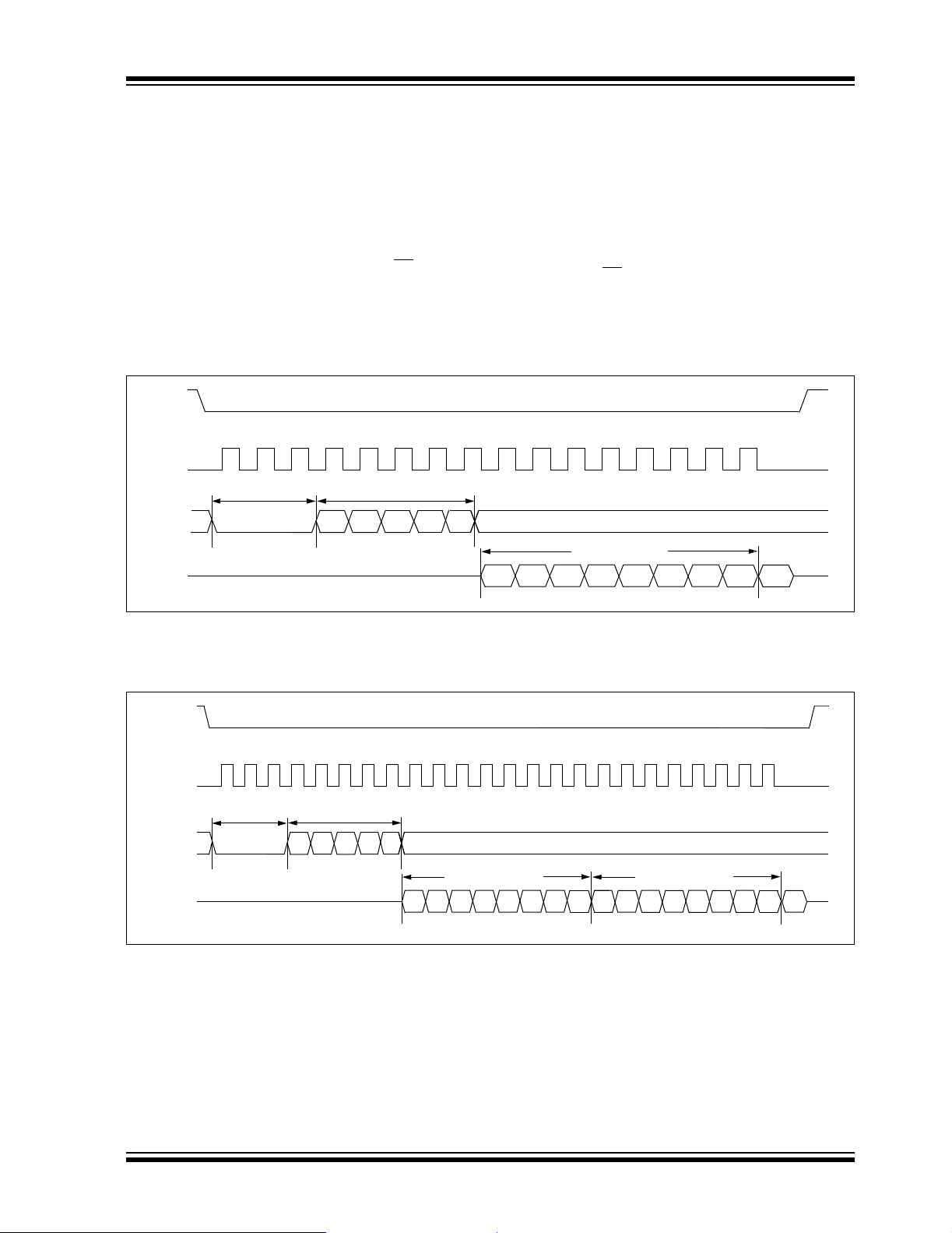
FIGURE 4-3: READ CONTROL REGISTER COMMAND SEQUENCE (ETH REGISTERS)
CS
0 234567891011121314151
SCK
Opcode Address
SI
High-Impedance State
SO
2034000 1
Data Out
76543210
FIGURE 4-4: READ CONTROL REGISTER COMMAND SEQUENCE
(MAC AND MII REGISTERS)
CS
0 23456789101112131415161718192021221
SCK
Opcode
SI
High-Impedance State
SO
Address
2034000 1
Dummy Byte
76543210
Data Byte Out
76543210
23
2004 Microchip Technology Inc. Advance Information DS39662A-page 27
Page 30
ENC28J60
4.2.2 READ BUFFER MEMORY COMMAND
The Read Buffer Memory (RBM) command allows the
host controller to read bytes from the integrated 8-Kbyte
transmit and receive buffer memory.
If the AUTOINC bit in the ECON2 register is set, the
ERDPT pointer will automatically increment to point to
the next address after the last bit of each byte is read.
The next address will normally be the current address
incremented by one. However, if the last byte in the
receive buffer is read (ERDPT = ERXND), the ERDPT
pointer will change to the beginning of the receive
buffer (ERXST). This allows the host controller to read
packets from the receive buffer in a continuous stream
without keeping trac k of when a wra paround is needed.
If AUTOINC is set when address 1FFFh is read and
ERXND does not point to thi s address, the read poin ter
will increment and wrap around to 0000h.
The RBM command is started by pulling the CS
The RBM opcode is then sent to the ENC28J60,
followed by the 5-bit c onst ant 1Ah . After the R BM co mmand and constant are sent, the data stored in the
memory pointed to by ERDPT will be shifted out MSb
first on the SO pin. If the host controller continues to
provide clocks on the SCK pin, without raising CS
byte pointed to by ERDP T will agai n be shifted o ut MSb
first on the SO pin. In this manner, with AUTOINC
enabled, it is possible to continuously read sequential
bytes from the buffer memory without any extra SPI
command overhead . The RBM c ommand is terminate d
by raising the CS
pin.
pin low.
, the
4.2.3 WRITE CONTROL REGISTER COMMAND
The Write Control Register (WCR) command allows
the host controller to write to any of the ETH, MA C and
MII Control registers in any order. The PHY registers
are written to via a special MII register interface (see
Section 3.3.2 “Writing PHY Registers” for more
information).
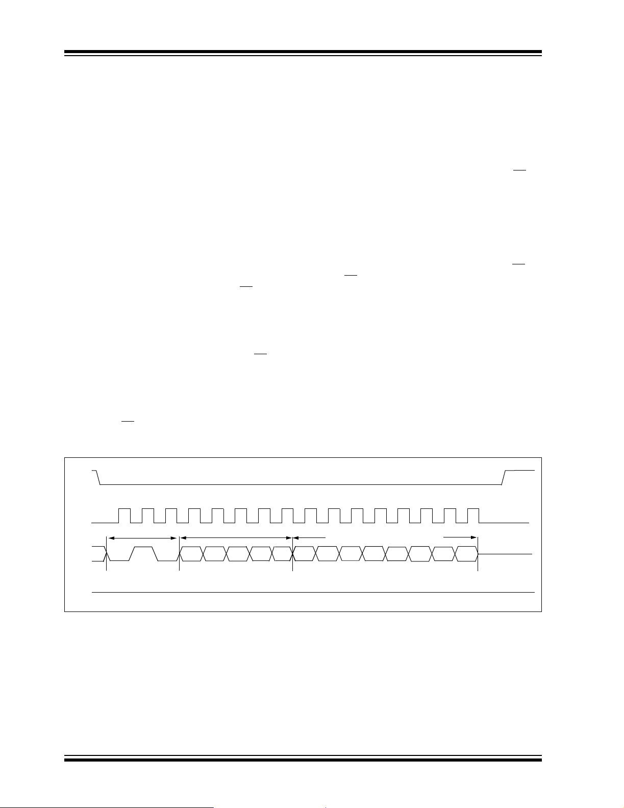
The WCR command is started by pulling the CS
low. The WCR opcode is then sent to the ENC28J60,
followed by a 5-bit address (A4 through A0). The 5-bit
address identifies any of the 32 control registers in the
current bank. After the WCR command and address
are sent, actual data that is to be written is sent, MSb
first. The data will be written to the addressed register
on the rising edge of the SCK line.
The WCR operation i s terminated by rais ing the CS
If the CS
loaded, the write will be aborted for that data byte.
Refer to the timing diagram in Figure 4-5 for a more
detailed illustration of the byte write sequence.
line is allowed to g o hi gh befo r e e igh t bi t s a re
pin
pin.
FIGURE 4-5: WRITE CONTROL REGISTER COMMAND SEQUENCE
CS
0 234567891011121314151
SCK
Opcode
SI
SO
Address
203A4010 1
Data Byte
D7 6 5 4
High-Impedance State
1D032
DS39662A-page 28 Advance Information 2004 Microchip Technology Inc.
Page 31

ENC28J60
4.2.4 WRITE BUFFER MEMORY COMMAND
The Write Buffer Memory (WBM) command allows the
host controller to write bytes to the integrated 8-Kbyte
transmit and receive buffer memory.
If the AUTOINC bit in the ECON2 register is set, after
the last bit of each byte is written, the EWRPT pointer
will automatically be incremented to point to the next
sequential address (current address + 1). If address
1FFFh is written with AUTOINC set, the write pointer
will increment to 0000h.
The WBM command is started by lowering the CS
pin.
The WBM opcode should then be sent to the
ENC28J60, followed by the 5-bit constant 1Ah. After
the WBM command and constant are sent, the data to
be stored in the memory pointed to by EWRPT should
be shifted out MSb first to the ENC28J60. After 8 data
bits are received, the write pointer will automatically
increment if AUTOINC is set. The host controller can
continue to provide clocks on the SCK pin and send
data on the SI pin, without raising CS
, to keep writing to
the memory. In this manner, with AUTOINC enabled, it
is possible to continuo usly write sequentia l bytes to the
buffer memory without any extra SPI command
overhead.
The WBM command is terminated by bringing up the
pin. Refer to Figure 4-6 for a detailed illustration of
CS
the write sequence.
4.2.5 BIT FIELD SET COMMAND
The Bit Field Set (BFS) comm and is used to set up to
8 bits in any of the ETH Control registers. Note that this
command cannot be used on the MAC registers, MII
registers, P HY registe rs or buf fer memo ry . The BFS command uses th e pr ovid ed data byt e to perf orm a b it-wise
OR operation on the addressed register contents.
The BFS command is started by pulling the CS
The BFS opcode is then sent, followed by a 5-bit
address (A4 through A0). The 5-bit address identifies
pin low.
any of the ETH registers in the current bank. After the
BFS command and address are sent, the data byte
containing the bit field set information should be sent,
MSb first. The supplied data will be logically ORed to
the content of the addressed register on the rising
edge of the SCK line for the D0 bit.
If the CS
line is brought high before eight bits are
loaded, the operation will be aborted for that data
byte. The BFS operation is terminated by raising the
pin.
CS
4.2.6 BIT FIELD CLEAR COMMAND
The Bit Field Clear (BFC) command is used to clear up
to 8 bits in any of the ETH Control registers. Note that
this command cannot be used on the MAC registers,
MII registers, PHY regis ters or buffer mem ory . The BFC
command uses the provided dat a byte to perform a bitwise NOTAND operation on the addressed register
contents. As an exam ple , if a reg ist er had the c ont ents
of F1h and the BFC command was executed with an
operand of 17h, then the register would be changed to
have the contents of E0h.
The BFC command is started by lowering the CS
The BFC opcode should then be sent, followed by a
5-bit address (A4 through A0). The 5-bit address
identifies any of the ETH registers in the current bank.
After the BFC command and address are sent, a data
byte containing the bit field clear information should
be sent, MSb first. The supplied data will be logically
inverted and subsequently ANDed to the contents of
the addressed register on the rising edge of the SCK
line for the D0 bit.
The BFC operation is terminated by bringing the CS
pin high. If CS is brought high before eight bits are
loaded, the operation will be aborted for that data
byte.
pin.
FIGURE 4-6: WRITE BUFFER MEMORY COMMAND SEQUENCE
CS
0 23456789101112131415161718192021221
SCK
Opcode Address
0011110
SI
SO
2004 Microchip Technology Inc. Advance Information DS39662A-page 29
1
7654
Data Byte 0
32
High-Impedance State
1D0
Data Byte 1
76543210
23
Page 32

ENC28J60
4.2.7 SYSTEM COMMAND
The System Command (SC) allows the host controller
to issue a System Soft Reset command. Unlike other
SPI commands, the SC i s on ly a s ing le- byte command
and does not operate on any register.
FIGURE 4-7: SYSTEM COMMAND SEQUENCE
CS
SCK
SI
SO
0 2345671
Opcode
Data Constant (1Fh)
High-Impedance State
The SC is started by pulling the CS
opcode should then be sent, followed by a 5-bit Soft
Reset command constant of 1Fh. The SC operation is
terminated by raising the CS
detailed ill ustration of the Syst em Command sequence.
For more information on SC’s Soft Reset, refer to
Section 11.2 “System Reset”.
1111111
1
pin low. The SC
pin. Figure 4-7 shows a
DS39662A-page 30 Advance Information 2004 Microchip Technology Inc.
Page 33
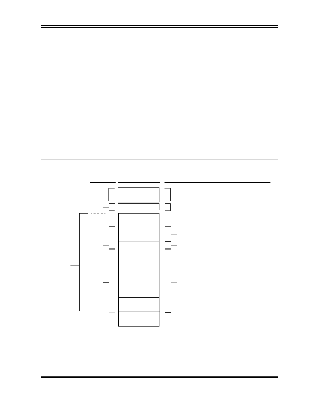
ENC28J60
5.0 ETHERNET OVERVIEW
Before discussing the use of the ENC28J60 as an
Ethernet interface, it may be helpful to review the
structure of a typical data frame. Users requiring more
information should refer to IEEE Standard 802.3 which
is the basis for the Ethernet protocol.
5.1 Packet Format
Normal IEEE 802.3 compliant Ethernet frames are
between 64 and 1518 byte s long. Th ey ar e made u p of
five or six diffe rent fiel ds: a dest ination MA C address , a
source MAC address, a typ e/length fie ld, data payloa d,
an optional padding field and a Cyclic Redundancy
Check (CRC). Additionally, when transmitted on the
Ethernet medium, a 7-byte preamble field and start-offrame delimiter byte are appended to the beginning of
the Ethernet packet. Thus, traffic seen on the twisted
pair cabling will appear as shown in Figure 5-1.
FIGURE 5-1: ETHERNET PACKET FORMAT
Number
of Bytes
Field
5.1.1 PREAMBLE/START-OF-FRAME
DELIMITER
When transmitting and receiving data with the
ENC28J60, the preamble and start of frame delimiter
bytes will automatically be generated or stripped from
the packets when th ey are tra nsmitted or received . The
host controller does not need to concern itself with
them. Normally, the host controller will also no t need to
concern itself with padding and the CRC which the
ENC28J60 will also be able to automatically generate
when transmitting and verify when receiving. The
padding and CRC fields will, however, be written into
the receive buffer when packets arrive, so they may be
evaluated by the host controller if need ed.
Comments
Used in the
calculation
of the FCS
7
1
6
6
2
46-1500
4
Preamble
SFD
DA
SA
Type/Length
Data
Padding
(1)
FCS
Filtered out by the MAC
Start-of-Frame Delimiter
(Filtered out by the MAC)
Destination Address,
such as Multicast, Broadcast or Unicast
Source Address
Type of Pack et or the Length of the Packet
Packet Payload
(with optional padding)
Frame Check Sequence – CRC
Note 1: The FCS is transmitted starting with bit31 and ending with bit 0.
2004 Microchip Technology Inc. Advance Information DS39662A-page 31
Page 34

ENC28J60
5.1.2 DESTINATION ADDRESS
The destinat ion address field is a 6- byte field fil led with
the MAC address of the device that the p acket is di rected
to. If the Least Significant bit in the first byte of the MAC
address is set, the address is a multicast destination. For
example, 01-00-00-00-F0-00 and 33-45-67-89-AB-CD
are multicast addresses, while 00-00-00-00-F0-00 and
32-45-67-89-AB-CD are not.
Packets with multicast destination addresses are
designed to arrive and be import ant to a sel ected group
of Ethernet nodes. If the destination address field is the
reserved multicast address, FF-FF-FF-FF-FF-FF, the
packet is a broadcast packet and it will be directed to
everyone sharing the network. If the Least Significant
bit in the first byte of the MAC address is clear, the
address is a unicast address and will be designed for
usage by only the addressed node.
The ENC28J60 incorporates receive filters which can
be used to discard or accept packets with multicast,
broadcast and/or unic ast des tinatio n addres ses. Whe n
transmitti ng packe ts, the host c ontrol ler is resp onsib le
for writing the desired destination address into the
transmit buffer.
5.1.3 SOURCE ADDRESS
The source address field is a 6-byte field filled with the
MAC address of the node which created the Ethernet
packet. Users of the ENC28J60 must generate a
unique MAC address for each controller used.
MAC addresses consist of two portions. The first three
bytes are known as the Organizationally Unique
Identifier (OUI). OUIs are distributed by the IEEE. The
last three bytes are address bytes at the discretion of
the company that purchased the OUI.
When transmitting packets, the assigned source MAC
address must be written into the transmit buffer by the
host controller. The ENC28J60 will not automatically
transmit the contents of the MAADR registers which
are used for the unicast receive filte r and uni ca st WOL
filter.
5.1.4 TYPE/LENGTH
The type/length field is a 2-byte field which defines
which protocol the following packet data belongs to.
Alternately, if the field is filled with the contents of
05DCh (1500) or any smaller number, the field is
considered a length fi eld and it specifies the amount of
non-padding da t a w h ic h fo llo w s in the data field. Users
implementing proprietary networks may choose to treat
this field as a leng th field, while applications implementing protocols such as the Internet Protocol (IP) or
Address Resolution Protocol (ARP), should program
this field with the appropriate type defined by the
protocol’s specification when transmitting packets.
5.1.5 DATA
The data field is a variable length field anywhere from 0
to 1500 bytes. Larger data packets will violate Ethernet
standards and will be dropped by most Ethernet nodes.
The ENC28J60, however, i s capab le of transmitti ng and
receiving larger packets when the Huge Frame Enable
bit is set (MACON3.HFRMEN = 1).
5.1.6 PADDING
The padding field is a variable length field added to
meet IEEE 802.3 specification requirements when
small data p aylo ads are used. The des tinati on, so urce,
type, data and padding of an Ethernet packet must be
no smaller than 60 bytes. Adding the required 4-byte
CRC field, packets must be no smaller than 64 bytes. If
the data field is le ss than 46 bytes long, a p add ing fiel d
is required.
When transmitting packets, the ENC28J60 automatically
generates z ero paddi ng if the MA CON3. PADCFG<2:0>
bits are conf ig ure d to do so. Otherwise, the host cont roller should ma nually add padding to the packe t before
transmitting it. The ENC28J60 will not prevent the
transmission of undersize packets should the host
controller command such an action.
When receiving packets, the ENC28J60 automatically
rejects packets which are less than 18 bytes. All packets 18 bytes and larger will be subject to the standard
receive filterin g criteria and may b e accepted as norma l
traffic.
5.1.7 CRC
The CRC field is a 4-byte fiel d which conta ins an industry standard 32-bit CRC calculated with the data from
the destination, source, type, data and padding fields.
When receiving packets, the ENC28J60 will check the
CRC of each incoming packet. If ERXFCON.CRCEN is
set, packets with invalid CRCs will automatically be
discarded. If CRCEN is clear and the packet meets all
other receive filtering criteria, the packet will be written
into the receive buffer and the host controller will be
able to determine if the CRC was valid by reading the
receive status vector (see Section 7.2 “Receiving
Packets”).
When transmitting packets, the ENC28J60 will automatically generate a valid CRC and transmit it if the
MACON3.PADCFG<2:0> bits are configured to cause
this. Otherwise, the host controller must generate the
CRC and place it in the transmit buffer. Given the complexity of calculating a CRC, it is high ly recommend ed
that the PADCFG bits be configured such that the
ENC28J60 will automatically generate the CRC field.
DS39662A-page 32 Advance Information 2004 Microchip Technology Inc.
Page 35

ENC28J60
6.0 INITIALIZATION
Before the ENC28J60 can be used to transmit and
receive packets, certain device settings must be initialized. Depending on the applicat ion, some co nfiguration
options may need to be changed. Normally, these task s
may be accomplished once after Reset and do not
need to be changed thereafter.
6.1 Receive Buffer
Before receiving any packets, the receive buffer must
be initialized by programming the ERXST and ERXND
pointers. All memory between and including the
ERXST and ERXND addre sses will be dedi cated to the
receive hardware. It is recommended that the ERXST
pointer be programmed with an even address.
Applications expecting large amounts of data and
frequent packet delivery may wish to allocate most of
the memory as the receive buffer. Applications that
may need to save older packets or have several
packets ready for transmission should allocate less
memory.
When programming the ERXST pointer, the ERXWRPT
registers will automatically be updated with the same
values. The address in ERXWRPT will be used as the
starting location when the receive hardware begins writing received data. For trackin g purposes, the ERXRDP T
registers should additionally be programmed with the
same value. To program ERXRDPT, the host controller
must write to ERXRDPTL first, followed by ERXRDPTH.
See Section 7.2.4 “Freeing Receive Buffer Space”
for more information.
6.2 Transmission Buffer
All memory which is not used by the receive buffer is
considered the tra ns mi ss io n buffer. Data whi ch i s to b e
transmitted should be written into any unused space.
After a packet is transmitted, however, the hardware
will write a seven-byte status vector into memory after
the last byte in the packet. Therefore, the host controller should leave at least seven bytes between each
packet and the beginning of the receive buffer. No
explicit action is required to initialize the transmission
buffer.
6.3 Receive Filters
The appropriate receive filters should be enabled or
disabled by writing to the ERXFCON register. See
Section 8.0 “Receive Filters” for information on how
to configure it.
6.4 Waiting For OST
If the initializati on proced ure is b eing ex ecuted imm ediately following a Power-on Rese t, th e ESTAT .C LKRDY
bit should be polled to make certain that enough time
has elapsed be fore pro ce edi ng to modify the MAC and
PHY registers. For more information on the OST, see
Section 2.2 “Oscillator Start-up Timer”.
2004 Microchip Technology Inc. Advance Information DS39662A-page 33
Page 36

ENC28J60
6.5 MAC Initialization Settings
Several of the MAC registers require configuration
during initialization. This only needs to be done once;
the order of programming is unimportant.
1. Clear the MARST bit in MACON2 to pull the
MAC out of Reset.
2. Set the MARXEN bit in MACON1 to enable the
MAC to receive fram es. If using f ull duplex, m ost
applications should also set TXPAUS and
RXPAUS to allow IEEE defined flow control to
function.
3. Configure the PADCFG, TXCRCEN and
FULDPX bits of MACON3. Most applications
should enable automatic padding to at least
60 bytes and always append a valid CRC. For
convenience, m any applica tions may w ish to set
the FRMLNEN bit as well to enab le frame length
status reporting. The FULDPX bit should be set
if the application will be connected to a
full-duplex configur ed remote n ode; otherwise, it
should be left clear.
4. Configure the bits in MACON4. Many
applications may not need to modify the Reset
default.
5. Program the MAMXFL registers with the maximum frame length to be permitted to b e received
or transmitted. Normal network nodes are
designed to handle packets that are 1518 bytes
or less.
6. Configure the Back-to-Back Inter-Packet Gap
register, MABBIPG. Most applications will program this register with 15h when Full-Duplex
mode is used and 12h when Half-Duplex mode
is used.
7. Configure the Non-Back-to-Back Inter-Packet
Gap register lo w byte, MAIPGL. Most applic ations
will program t hi s reg is te r wi th 12 h.
8. If half duplex is used, the Non-Back-to-Back
Inter-Packet Gap register high byte, MAIPGH,
should be programmed. Most applications will
program this register to 0Ch.
9. If Half-Duplex mode is used, program the
Retransmission and Collision Window registers,
MACLCON1 and MACLCON2. Most applications
will not need to change the default Reset values.
If the network is spread over exceptionally long
cables, the default value of MACLCON2 may
need to be increased.
10. Program the local MAC address into the
MAADR0:MAADR5 registers.
REGISTER 6-1: MACON1: MAC CONTROL REGISTER 1
U-0 U-0 U-0 R/W-0 R/W-0 R/W-0 R/W-0 R/W-0
— — — LOOPBK TXPAUS RXPAUS PASSALL MARXEN
bit 7 bit 0
bit 7-5 Unimplemented: Read as ‘0’
bit 4 LOOPBK: MAC Loopback Enable bit
1 = All data transmitted by the MAC will be looped back to the MAC
0 = Normal operation
bit 3 TXPAUS: Pause Control Frame Transmission Enable bit
1 = Allow the MAC to transmit pause control frames (needed for flow control in full duplex)
0 = Disallow pause frame transmissions
bit 2 RXPAUS: Pause Control Frame Reception Enable bit
1 = Inhibit transmissions when pause control frames are received (normal operation)
0 = Ignore pause control frames which are received
bit 1 PASSALL: Pass All Received Frames Enable bit
1 = Control frames received by th e MAC will be wirtten into the receive buffer if not filtered out
0 = Control frames will be discarded after being processed by the MAC (normal operation)
bit 0 MARXEN: MAC Receive Enable bit
1 = Enable packets to be received by the MAC
0 = Disable pack et reception
Legend:
R = Readable bit W = Writable bit U = Unimplemented bit, read as ‘0’
-n = Value at POR ‘1’ = Bit is set ‘0’ = Bit is cleared x = Bit is unknown
DS39662A-page 34 Advance Information 2004 Microchip Technology Inc.
Page 37

REGISTER 6-2: MACON3: MAC CONTROL REGISTER 3
R/W-0 R/W-0 R/W-0 R/W-0 R/W-0 R/W-0 R/W-0 R/W-0
P ADCFG2 P ADCFG1 PADCFG0 TXCRCEN PHDRLEN HFRMEN FRMLNEN FULDPX
bit 7 bit 0
bit 7-5 PADCFG2:PACDFG0: Automatic Pad and CRC Configurat ion bits
111 = All short frames will be zero padded to 64 bytes and a valid CRC will then be appended
110 = No automatic padding of short frames
101 = MAC will automatically detect VLAN Protocol frames which have a 8100h type field and
automatically pad to 64 bytes. If the frame is not a VLAN frame, it will be padded to
60 bytes. After padding, a valid CRC will be appended.
100 = No automatic padding of short frames
011 = All short frames will be zero padded to 64 bytes and a valid CRC will then be appended
010 = No automatic padding of short frames
001 = All short frames will be zero padded to 60 bytes and a valid CRC will then be appended
000 = No automatic padding of short frames
bit 4 TXCRCEN: Transmit CRC Enable bit
1 = MAC will apend a valid CRC to all frames transmitted regardless of PADCFG. TXCRCEN
must be set if PADCFG specifies that a valid CRC will be appended.
0 = MAC will not append a CRC. The last 4 bytes will be checked and if it is an invalid CRC, it
will be reported in the transmit status vector.
bit 3 PHDRLEN: Proprietary Header Enable bit
1 = Frames presen t e d to t h e M AC co ntai n a 4 -b yt e pr op ri e tary he a de r w h ic h wil l no t b e us ed
when calculating the CRC
0 = No proprietary header is present. The CRC will cover all data (normal operation).
bit 2 HFRMEN: Huge Frame Enable bit
1 = Frames of any size will be allowed to be transmitted and receieved
0 = Frames bigger than MAMXFL will be aborted when transmitted or received
bit 1 FRMLNEN: Frame Length Checking Enable bit
1 = The type/length field of transmitte d and recei ved fram es will be ch ecke d. If it represent s a
length, the frame size will be compared and mismatches will be reported in the
transmit/receive status vector.
0 = Frame lengths will not be compared with the type/length field
bit 0 FULDPX: MAC Full-Duplex Enable bit
1 = MAC will operate in full-duplex. PHCON1.PDPXMD must also be set.
0 = MAC will operate in half-duplex. PHCON1.PDPXMD must also be clear.
ENC28J60
Legend:
R = Readable bit W = Writable bit U = Unimplemented bit, read as ‘0’
-n = Value at POR ‘1’ = Bit is set ‘0’ = Bit is cleared x = Bit is unknown
2004 Microchip Technology Inc. Advance Information DS39662A-page 35
Page 38

ENC28J60
REGISTER 6-3: MACON4: MAC CONTROL REGISTER 4
U-0 R/W-0 R/W-0 R/W-0 U-0 U-0 R/W-0 R/W-0
— DEFER BPEN NOBKOFF — — LONGPRE PUREPRE
bit 7 bit 0
bit 7 Unimplemented: Read as ‘0’
bit 6 DEFER: Defer Transmission Enable bit (applies to half duplex only)
1 = When the medium is occupied, the MAC will wait indefinately for it to become free when
attempting to transmit
0 = When the medium is occupied, the MAC will abort the transmission after the excessive
deferral limit is reached (2.4287 ms)
bit 5 BPEN: No Backoff During Back Pressure Enable bit (applies to half duplex only)
1 = After incidentally causing a collission during back pressure, the MAC will immediately
begin retransmitting
0 = After incidentally causing a collision during back pressure, the MAC will delay using the
binary exponential backoff algorithm before attempting to retransmit (normal operation)
bit 4 NOBKOFF: No Backoff Enable bit (applies to half duplex only)
1 = After any collision, the MAC will immediately begin retransmitting
0 = After any collision, the MAC will delay using the binary exponential backoff algorithm
before attempting to retransmit (normal operation)
bit 3-2 Unimplemented: Read as ‘0’
bit 1 LONGPRE: Long Preamble Enforcement Enable bit
1 = Received packets will be rejected if they are preceded by 12 or more bytes of preamble
0 = Received packets will not be rejected if they have 12 or more bytes of preamble (normal
operation)
bit 0 PUREPRE: Pure Preamble Enforcement Enable bit
1 = The preamble of received packets will be checked against 55h. If it contains an error, the
packet will be discarded.
0 = The preamble of received packets will not be checked
Legend:
R = Readable bit W = Writable bit U = Unimplemented bit, read as ‘0’
-n = Value at POR ‘1’ = Bit is set ‘0’ = Bit is cleared x = Bit is unknown
DS39662A-page 36 Advance Information 2004 Microchip Technology Inc.
Page 39

ENC28J60
REGISTER 6-4: MABBIPG: MAC BACK-TO-BACK INTER-PACKET GAP REGISTER
U-0 R/W-0 R/W-0 R/W-0 R/W-0 R/W-0 R/W-0 R/W-0
— BBIPG6 BBIPG5 BBIPG4 BBIPG3 BBIPG2 BBIPG1 BBIPG0
bit 7 bit 0
bit 7 Unimplemented: Read as ‘0’
bit 6-0 BBIPG6:BBIPG0: Back-to-Back Inter-Packet Gap Delay Time bits
MACON3.FULDPX = 1:
When
Nibble time offset delay between the end of one transmiss io n and the beginning of the next in
a back-to-back sequence. The register value should be programmed to the desired period in
nibble times minus 3. The recommended setting is 15h which represents the minimum IEEE
specified Inter-Packet Ga p (IP G) of 9.6 µs.
When MACON3.FULDP
Nibble time offset delay between the end of one transmiss io n and the beginning of the next in
a back-to-back sequence. The register value should be programmed to the desired period in
nibble times minus 6. The recommended setting is 12h which represents the minimum IEEE
specified Inter-Packet Ga p (IP G) of 9.6 µs.
Legend:
R = Readable bit W = Writable bit U = Unimplemented bit, read as ‘0’
-n = Value at POR ‘1’ = Bit is set ‘0’ = Bit is cleared x = Bit is unknown
X = 0:
2004 Microchip Technology Inc. Advance Information DS39662A-page 37
Page 40

ENC28J60
6.6 PHY Initialization Settings
Depending on the application, bits in three of the PHY
module’s registers may also require configuration.
The PHCON1.PDPXMD bit partially controls the
device’s half/fu ll-dupl ex con figurati on. No rmally, this bit
is initialized correctly by the external circuitry (see
Section 2.6 “LED Configuration”). If the external
circuitry is not present or incorrect, however, the host
controller must program the bit properly. Alternatively,
for an externally conf ig urab le s yste m, the PD PXMD b it
may be read and the FULDPX bit be programmed to
match.
For proper duplex operation, the PHCON1.PDPXMD
bit must also match th e value of the MACON 3.FULDPX
bit.
REGISTER 6-5: PHCON2: PHY CONTROL REGISTER 2
U-0 R/W-0 R/W-0 R/W-x R/W-x R/W-0 R/W-0 R/W-0
— FRCLNK TXDIS r r JABBER r HDLDIS
bit 15
R/W-x R/W-x R/W-x R/W-x R/W-x R/W-x R/W-x R/W-x
rrrrrrrr
bit 7 bit 0
If using half duplex, the host controller may wish to set
the PHCON2.HDLDIS bit to prevent automatic
loopback of the data which is transmitted.
The PHY register, PHLCON, controls the outputs of
LEDA and LEDB. If an application requires a LED
configuration other than the default, PHLCON must be
altered to match the new requireme nts. The settings for
LED operation are discussed in Section 2.6 “LED
Configuration”. The PHLCON register is shown in
Register 2-2 (page 9).
bit 15 Unimplemented: Read as ‘0’
bit 14 FRCLNK: PHY Force Linkup bit
1 = Force linkup even when no link partner is detected
0 = Normal operation
bit 13 TXDIS: Twisted Pair Transmitter Disable bit
1 = Disable twisted pair transmitter
0 = Normal operation
bit 12-11 Reserved: Write as ‘0’
bit 10 JABBER: Jabber Correction Disable bit
1 = Disable jabber correction
0 = Normal operation
bit 9 Reserved: Write as ‘0’
bit 8 HDLDIS: PHY Half-Duplex Loopback Disable bit
When
PHCON1.PDPXMD = 1 or PHCON1.PLOOPBK = 1:
This bit is ignored.
PHCON1.PDPXMD = 0 and PHCON1.PLOOPBK = 0:
When
1 = Transmitted data will only be sent out on the twisted pair interface
0 = Transmitted data will be looped back to the MAC and sent out the twisted pair interface
bit 7-0 Reserved: Write as ‘0’
Legend: r = Reserved bit
R = Readable bit W = Writable bit U = Unimplemented bit, read as ‘0’
-n = Value at POR ‘1’ = Bit is set ‘0’ = Bit is cleared x = Bit is unknown
DS39662A-page 38 Advance Information 2004 Microchip Technology Inc.
Page 41

ENC28J60
7.0 TRANSMITTING AND RECEIVING PACKETS
7.1 Transmitting Packets
The MAC inside the ENC28J60 will automatically generate the preamble and start-of-frame delimiter fields when
transmitting. Additionally, the MAC can generate any
padding (if needed) and the CRC if configured to do so.
The host controller must generate and write all other
frame fields into the buffer memory for transmission.
Additionally, the ENC28J60 requires a single per packet
control byte to precede the packet for transmission. The
per packet control byte is organized as shown in
Figure 7-1. Before transmitting packets, the MAC
registers which alter the transmission characteristics
should be initialized as documented in Section 6.0
“Initialization”.
For an exa mple of how the en tire trans mit pac ket a nd
results will look in memory, see Figure 7-2.
FIGURE 7-1: FORMAT FOR PER PACKET CONTROL BYTES
— — — — PHUGEEN PPADEN PCRCEN POVERRIDE
bit 7 bit 0
bit 7-4 Unused
bit 3 PHUGEEN: Per Packet Huge Frame Enable bit
When POVERRIDE =
1 = The packet will be transmitted in whole
0 = The MAC will transmit up to the number of bytes specified by MAMX FL. If the packet is larger
than MAMXFL, it will be aborted after MAMXFL is reached.
When POVERRIDE =
This bit is ignored.
bit 2 PPADEN: Per Packet Padding Enable bit
When POVERRIDE = 1:
1 = The packet will be zero padded to 60 bytes if it is less than 60 bytes
0 = The packet will be trasmitted without adding any padding bytes
When POVERRIDE =
This bit is ignored.
bit 1 PCRCEN: Per Packet CRC Enable bit
When POVERRIDE = 1:
1 = A valid CRC will be calculated and attached to the frame
0 = No CRC will be appended. The last 4 bytes of the frame will be checked for validity as a
CRC.
When POVERRIDE =
This bit is ignored.
bit 0 POVERRIDE: Per Packet Override bit
1 = The values of PCRCEN, PPADEN and PHUG EEN will override th e confi guratio n defin ed by
MACON3
0 = The values in MACON3 will be used to determine how the packet will be transmitted
1:
0:
0:
0:
2004 Microchip Technology Inc. Advance Information DS39662A-page 39
Page 42

ENC28J60
FIGURE 7-2: SAMPLE TRANSMIT PACKET LAYOUT
Buffer Pointers
ETXST = 0120h
ETXND = 0156h
Address Memory Description
0120h
0121h
0122h
0156h
0157h
0158h
0159h
016Ah
016Bh
016Ch
016Dh
016Eh
0Eh
data[1]
data[2]
data[m]
tsv[7:0]
tsv[15:8]
tsv[23:16]
tsv[31:24]
tsv[39:32]
tsv[47:40]
tsv[51:48]
Control
Data Packet
Status Vector
PHUGEEN, PPADEN,
PCRCEN and POVERRIDE
Destination Address,
Source Address,
Type/Length and Data
Status Vector
Written by the Hardware
Start of the Next Packet
T o a chieve the e xample layout shown in F igure 7-2 and
to transmit a packet, the host controller should:
1. Appropriately program the ETXST pointer to
point to an unused location in memory. It will
point to the per packet control byte. In the
example, it would be p rogramme d to 0120h. It is
recommended that an even add ress be used for
ETXST.
2. Use the WBM SPI command to write the per
packet control byte, the destinati on address, the
source MAC address, the type/length and the
data payload.
3. Appropriately program the ETXND pointer. It
should point to t he l as t by te in the data payload.
In the example, it would be programmed to
0156h.
4. Clear EIR.TXIF, set EIE.TXIE and set EIE.INTIE
to enable an interrupt when done (if desired).
5. Start the transmission process by setting
ECON1.TXRTS.
If a DMA operation wa s in progress wh ile the TXRTS b it
was set, the ENC28J60 will wait until the DMA operation is complete before attempting to transmit the
packet. This possible delay is required because the
DMA and transmission engine sh are the same mem ory
access port. Similarly, if the DMAST bit in ECON1 is set
after TXRTS is already set, the DMA will wait until the
TXRTS bit becomes clear be fore doing anything . While
the transmission is in progress, none of the unshaded
bits (except for the EECON1 reg ister’s bits) in Table 7-2
should be changed. Additionally, none of the bytes to be
transmitted should be read or written to through the SPI.
If the host controller wishes to cancel the transmission,
it can clear the TXRTS bit.
When the packet is finished transm itting or was aborte d
due to an error/cancellation, the ECON1.TXRTS bit will
be cleared, a seven-byte transmit status vector will be
written to the location pointed to by ETXND + 1, the
EIR.TXIF will be set and an interrupt will be generated
(if enabled). The ETXST and ETXND pointers will not
be modified. To check if the packet was successfully
transmitted, the ESTAT.TXABRT bit should be read. If
it was set, the host controller may interrogate the
ESTAT.LATECOL bit in addition to the various fields in
the transmit status vector to determine the cause. The
transmit status vector is organized as shown in
Table 7-1. Multi-byte fields are written in little-endian
format.
DS39662A-page 40 Advance Information 2004 Microchip Technology Inc.
Page 43

ENC28J60
TABLE 7-1: TRANSMIT STATUS VECTORS
Bit Field Description
63-52 Zero 0
51 Transmit VLAN Tagged Frame Frame’s length/type field contained 8100h which is the VLAN protocol
identifier.
50 Backpressure Applied Carrier sense method backpressure was previously applie d.
49 Transmit Pause Control Frame The frame transmitted was a control frame with a valid pause opcode.
48 Transmit Control Frame The frame transmitted was a control frame.
47-32 Total Bytes Transmitted on Wire Total bytes transmitted on the wire for the current packet, including all
bytes from collided attempts.
31 Transmit Underrun Reserved. This bit will always be ‘0’.
30 Transmit Giant Byte count for frame was greater than MAMXFL.
29 Transmit Late Collision Collision occurred beyond the collision window (MACLCON2).
28 Transmit Excessive Collision Packet was aborted after the number of collisions exceeded the
retransmission maximum (MACLCON1) .
27 Transmit Excessive Defer Packet was deferred in excess of 24,287 bit times (2.4287ms).
26 Transmit Packet Defer Packet was d eferred for at le ast one atte mpt but l ess tha n an e xces sive
defer.
25 Transmit Broadcast Packet’s destination address was a broadcast address.
24 Transmit Multicast Packet’s destination address was a multicast address.
23 Transmit Done Transmission of the packet was completed.
22 Transmit Length Out of Range Indicates that frame type/length field was larger than 1500 bytes (type
field).
21 Transmit Length Check Error Indicates that frame length field value in the packet does not match the
actual data byte length and is not a type field. MACON3.FRMLNEN
must be set to get this error .
20 Transmit CRC Error The attached CRC in the packet did not match the internally generated
CRC.
19-16 Transmit Collision Count Number of collisions the current packet incurred during transmission
attempts. It app lies to s uccessful ly transm itted p acket s and a s such, will
not show the possible maximum count of 16 collisions.
15-0 Transmit Byte Count Total bytes in frame not counting collided bytes.
2004 Microchip Technology Inc. Advance Information DS39662A-page 41
Page 44

ENC28J60
TABLE 7-2: SUMMARY OF REGISTERS USED FOR PACKET TRANSMISSION
Register
Name
EIE INTIE
EIR
ESTAT INT
ECON1 TXRST
ETXSTL TX Start Low Byte (ETXST<7:0>) 13
ETXSTH
ETXNDL TX End Low Byte (ETXND<7:0>) 13
ETXNDH
MACON1
MACON2 MARST RNDRST
MACON3 PADCFG2 PADCFG1 PADCFG0 TXCRCEN PHDRLEN HFRMEN FRMLNEN FULDPX 14
MACON4
MABBIPG
MAIPGL
MAIPGH
MACLCON1
MACLCON2
MAMXFLL Maximum Frame Length Low Byte (MAMXFL<7:0>) 14
MAMXFLH Maximum Frame Length High Byte (MAMXFL<15:8>) 14
MAPHSUP
Legend: — = unimplemented, r = reserved bit. Shaded cells are not used.
Bit 7 Bit 6 Bit 5 Bit 4 Bit 3 Bit 2 Bit 1 Bit 0
PKTIE DM AIE LINKIE TXIE WOLIE TXERIE RXERIE 13
— PKTIF DMAIF LINKIF TXIF WOLIF TXERIF RXERIF 13
r rLATECOL— RXBUSY TXABRT CLKRDY 13
RXRST DMAST CSUMEN TXRTS RXEN BSEL1 BSEL0 13
— — — TX Start High Byte (ETXST<12:8>) 13
— — — TX End High Byte (ETXND<12:8>) 13
— — — LOOPBK TXPAUS RXPAUS PASSALL MARXEN 14
— — MARXRST RFUNRST MATXRST TFUNRS T 14
— DEFER BPEN NOBKOFF — — LONGPRE PUREPRE 14
— Back-to-Back Inter-Packet Gap (BBIPG<6:0>) 14
— Non-Back-to-Back Inter-Packet Gap Low Byte (MAIPGL<6:0>) 14
— Non-Back-to-Back Inter-P acket Gap High Byte (MAIPGH<6:0>) 14
— — — — Retransmission Maximum (RETMAX<3:0>) 14
— — Collision Window (COLWIN<5:0>) 14
r — — rRSTRMII— — r14
Reset
Values
on page
DS39662A-page 42 Advance Information 2004 Microchip Technology Inc.
Page 45

ENC28J60
7.2 Receiving Packets
7.2.1 ENABLING RECEPTION
Assuming that the receive buffer has been initialized,
the MAC has been prop erly c onfigu red a nd the receive
filters have been configured to receive Ethernet
packets, the host con troll er sho uld :
1. If an interrupt is desired whenever a packet is
received, set EIE.PKTIE and EIE.INTIE.
2. If an interrupt is desired whenever a packet is
dropped due to insufficient buffer space, clear
EIR.RXERIF and set both EIE.RXERIE and
EIE.INTIE
3. Enable reception by setting ECON1.RXEN.
After setting RXEN, the Duplex mode and the receive
buffer start and end pointers should not be modified.
Additionally, to prevent unexpected packets from arriving, it is recommended that RXEN be cleared before
altering the rec eive filter configurat ion (ERXFC ON) and
MAC address.
After reception is enabled, packets which are not
filtered out will be written int o the circular receive bu ffer .
Any packet which does not meet the necessary filter
criteria will b e d is car ded a n d t he host controller will not
have any means of identif ying that a packet wa s thrown
away. When a packet is accepted and completely
written into the buffer, the EPKTCNT register will increment, the EIR.PKTIF bit will be set, an interrupt will be
generated (if enabled) and the hardware write pointer,
ERXWRPT, will automatically advance.
7.2.2 RECEIVE PACKET LAYOUT
Figure 7-3 shows the layout of a received packet. The
packets are preceded by a six-byte header which
contains a ne xt pac ket po int er, in add iti on t o a rec eiv e
status vector which contains receive statistics, including the packet’s size. This receive status vector is
shown in Table 7-3.
If the last byte in the packet ends on an odd value
address, the hardw are will au tomatica lly add a pad ding
byte when advancing the hardware write pointer. As
such, all packets will start on an even boundary.
FIGURE 7-3: SAMPLE RECEIVE PACKET LAYOUT
Address Memory Description
Packet N
Packet N + 1
Packet N + 2
101Fh
1020h
1021h
1022h
1023h
1024h
1025h
1026h
1027h
1059h
106Ah
106Bh
106Ch
106Dh
106Eh
10h
6Eh
rsv[7:0]
rsv[15:8]
rsv[23:16]
rsv[30:24]
data[1]
data[2]
data[m – 3]
data[m – 2]
data[m – 1]
data[m]
Low Byte
High Byte
status[7:0]
status[15:8]
status[23:16]
status[31:24]
crc[31:24]
crc[23:16]
crc[15:8]
crc[7:0]
End of the Previous Packet
Next Packet Pointer
Receive Status Vector
Packet Data: destination addres s,
source address, type/leng th, data ,
padding, CRC
Byte Skipped to Ensure
Even Buffer Address
Start of the Next Packet
2004 Microchip Technology Inc. Advance Information DS39662A-page 43
Page 46

ENC28J60
TABLE 7-3: RECEIVE STATUS VECTOR
Bit Field Description
31 Zero 0
30 Receive VLAN Type Detected Current frame was recognized as a VLAN tagged frame.
29 Receive Unknown Opcode Current frame was recognized as a control frame but it contained an
unknown opcode.
28 Receive Pause Control Frame Current frame was reco gni ze d as a con trol fr am e co nt a ini ng a v ali d pause
frame opcode and a valid destination address.
27 Receive Control Frame Current frame was recognized as a control frame for having a valid
type/length designating it as a control frame.
26 Dribble Nibble Indicates that after the end of this packet, an additional 1 to 7 bits were
received. The extra bits were thrown away.
25 Receive Broadcast Packet Indicates packet received had a valid broadcast address.
24 Receive Multicast Packet Indicates packet received had a valid multicast address.
23 Received Ok Indicates that at the packet had a valid CRC and no symbol errors.
22 Length Out of Range Indicates that frame type/length field was larger than 1500 bytes (type field).
21 Length Check Error Indicates that frame length field value in the packet does not match the
actual data byte length and specifies a valid length.
20 CRC Error Indicates that frame CRC field value does not match the CRC calculated
by the MAC.
19 Reserved
18 Carrier Event Previously Seen Indicates that at some time since the last receive, a carrier event was
detected. The carrier event is not associated with this packet. A carrier
event is activity on the receive channel that does not result in a packet
receive attempt being made.
17 Reserved
16 Long Event/Drop Event Indicates a packet over 50,000 bit times occurred or that a packet was
dropped since the last receive.
15-0 Received Byte Count Indicates length of the received frame. This includes the destination
address, source address, type/length, data, padding and CRC fields. This
field is stored in little-endian format.
7.2.3 READING RECEIVED PACKETS
To process the packet, the host controller will normally
use the RBM SPI command and start reading from the
beginning of the next packet pointer. The host controller
will save the next packet pointer, any necessary bytes
from the receive status vector and then proceed to read
the actual packet contents. If ECON2.AUTOINC is set, it
will be able to sequentially read the entire pa cket without
ever modifying the ERDPT registers. The read pointer
would automatically wrap at the end of the circular
receive buffer to the beginning.
In the event that the application needed to do random
access to the packet, i t would be nece ssary to manually calculate the proper ERDPT, taking care to not
exceed the end of the re ceive buf fer if the packe t spans
the ERXND-to-ERXST buf fer boundary. In other words,
given the packet st art address and a desired of fset, the
application should follow the logic shown in
Example 7-1.
EXAMPLE 7-1: RANDOM ACCESS ADDRESS CALCULATION
if Packet Start Address + Offset > ERXND, then
ERDPT = Packet Start Addres s + Offset – (ERXND – ERXST + 1)
else
ERDPT = Packet Start Address + Offset
DS39662A-page 44 Advance Information 2004 Microchip Technology Inc.
Page 47

ENC28J60
7.2.4 FREEING RECEIVE BUFFER SPACE
After the host control ler has processed a packet (or p art
of the packet) and wishes to fre e the bu ff er sp ace used
by the processed data, the host controller must
advance the receive buffer read pointer, ERXRDPT.
The ENC28J60 will always write up to, but not including, the memory pointed to by the receive buffer read
pointer . If the EN C28J60 eve r attempt s to overw rite the
receive buffer read pointer location, the packet in
progress will be aborted, the EIR.RXERIF will be set
and an interrupt will be generated (if enabled). In this
manner, the hardware will never overwrite unprocessed packets. Normally, the ERXRDPT will be
advanced to the value pointed to by the next packet
pointer which precedes the rec eive status vector for the
current packet. Following such a procedure will not
require any pointer c alculations to ac count for wrappin g
at the end of the circular receive buffer.
The receive buffer read pointer low byte (ERXRDPTL
register) is internally buffered to prevent the pointer
from moving when only one byte is upd ated through the
SPI. To move ERXRDPT, the host controller must write
to ERXRDPTL first. The write will update the internal
buffer but will not affect the register. When the host
controller writes to ERXRDPTH, the internally buffered
low byte will be loaded into the ERXRDPTL register at
the same time. The ERXRDPT bytes can be read in
any order. When they are read, the actual value of the
registers will be returned. As a result, the buffered low
byte is not readable.
In addition to a dvancing t he recei ve buf fer re ad pointe r ,
after each packet is ful ly proc es se d, th e ho st c ont roller
must write a ‘ 1’ to the ECON2.PKTDEC bit. Doing so
will cause the EPKTCNT register to decrement by 1.
After decrementing, if EPKTCNT is ‘0’, the EIR.PKTIF
flag will automatically be cleared. Otherwise, it will
remain set, indicat ing that addi tional packets are in the
receive buffer and are waiting to be processed.
Attempts to decre ment EPKTCNT b elow 0 are ignored.
Additionally, if the EPKTCNT register ever maximizes
at 255, all new packets which are received will be
aborted, even if buffer space is available. To indicate
the error, the EIR .RXERI F will b e set and an in terrup t
will be generated (i f enabled). To preven t this condi tion,
the host controller must properly decrement the
counter whenever a packet is processed.
Because only one pointer is available to control buffer
area ownership, the hos t controller m ust proces s packets in the order they are received. If the host controller
wishes to save a packet to be processed later, it should
copy the packet to an unused location in memory. It
may accomplish this efficiently using the integrated
DMA controller (see Section 13.0 “Direct Memory
Access Controller”).
7.2.5 RECEIVE BUFFER FREE SPACE
At any time the host controller wishes to know how
much receive buffer space is remaining, it should read
the hardware write pointer (ERXWRPT registers) and
compare it with the ERXRDPT registers. Combined
with the known size of the receive bu ffer , the free space
can be derived.
Note: The ERXWRPT registers only update
when a packet has been successfully
received. If the host controller reads it jus t
before another pa cket is to be succ essfully
completed, the value returned could be
stale and of f by the ma ximum f rame length
permitted (MAMXFLN) plus 7. Furthermore, as the host controller reads one
byte of ERXWRPT, a new packet may
arrive and update the pointer before the
host controller has an opportunity to read
the other byte of ERXWRPT.
When reading the ERXWRPT register with the receive
hardware enabled, special care must be taken to
ensure the low and high bytes are read as a matching
set.
To be assured that a mat ching set is obtained:
1. Read the EPKTCNT register and save its
contents.
2. Read ERXWRPTL and ERXWRPTH.
3. Read t he EPKTCNT register again.
4. Compare the tw o packet counts . If th ey are not
the same, go back to step 2.
With the hardware write pointer obtained, the free
space can be cal culated as shown in Example 7-2. The
hardware prohibits moving the write pointer to the
same value occupied by ERXRDPT (except when the
buffer pointers are being configured), so at least one
byte will always go unused in the buffer. The example
calculation reflects the lost byte.
EXAMPLE 7-2: RECEIVE BUFFER FREE SPACE CALCULATION
if ERXWRPT > ERXRDPT, then
Free Space = (ERXND – ERXST) – (ERXWRPT – ERXRDPT)
else if ERXWRPT = ERXRDPT, then
Free Space = (ERXND – ERXST)
else
Free Space = ERXRDPT – ERXWRPT – 1
2004 Microchip Technology Inc. Advance Information DS39662A-page 45
Page 48

ENC28J60
TABLE 7-4: SUMMARY OF REGISTERS USED FOR PACKET RECEPTION
Register
Name
EIE INTIE PKTIE
EIR
ESTAT INT
ECON2
ECON1
ERXSTL RX Start Low Byte (ERXST<7:0>) 13
ERXSTH
ERXNDL RX End Low Byte (ERXND<7:0>) 13
ERXNDH
ERXRDPTL RX RD Pointer Low Byte (ERXRDPT<7:0>) 13
ERXRDPTH
ERXFCON UCEN A NDOR CRCEN PMEN MPEN HTEN MCEN BCEN 14
EPKTCNT Ethernet Pack et Count 14
MACON1 — — — LOOPBK
MACON2 MARST
MACON3
MACON4
MAMXFLL Maximum Frame Length Low Byte (MAMXFL<7:0>) 14
MAMXFLH Maximum Frame Length High Byte (MAMXFL<15:8>) 14
MAPHSUP
Legend: — = unimplemented, r = reserved bit. Shaded cells are not used.
Bit 7 Bit 6 Bit 5 Bit 4 Bit 3 Bit 2 Bit 1 Bit 0
DMAIE LINKIE TXIE WOLIE TXERIE RXERIE 13
—PKTIFDMAIF LINKIF TXIF WOLIF TXERIF RXERIF 13
r r LATECOL —RXBUSYTXABRT CLKRDY 13
AUTOINC PKTDEC PWRSV — VRPS — — —13
TXRST RXRST DMAST CSUMEN TXRTS RXEN BSEL1 BSEL0 13
— — — RX Start High Byte (ERXST<12:8>) 13
— — — RX End High Byte (ERXND<12:8>) 13
— — — RX RD Pointer High Byte (ERXRDPT<12:8>) 13
TXPAUS RXPAUS PASSALL MARXEN 14
RNDRST — — MARXRST RFUNRST MATXRST TFUNRST 14
PADCFG2 PADCFG1 PADCFG0 TXCRCEN PHDRLEN HFRMEN FRMLNEN FULDPX 14
— DEFER BPEN NOBKOFF — — LONGPRE PUREPRE 14
r — — rRSTRMII— — r14
Reset
Values
on page
DS39662A-page 46 Advance Information 2004 Microchip Technology Inc.
Page 49

ENC28J60
8.0 RECEIVE FILTERS
To minimize the processing requirements of the host
controller , th e ENC28J 60 incorp orates sev eral dif ferent
receive filters which can automatically reject packets
which are not needed. Six different types of packet
filters are implemented:
• Unicast
• Pattern Match
•Magic Packet™
• Hash Table
• Multicast
• Broadcast
The individual filters are all configured by the ERXFCON
register (Register 8-1). More than one filter can be active
at any given time. Additionally, the filters can be configured by the ANDOR bit to either logically AND, or
logically OR, the tests of several filters. In other words,
the filters may be set so that only packets accepted by
all active filters are accepted, or a packet accepted by
any one filter is accepted. The flowcharts in Figure 8-1
and Figure 8-2 show the effect that each of the filters will
have depending on the setting of ANDOR.
The device can enter Promiscuous mode and receive
all packets by clearing the ERXFCON register. The
proper setting of the register will depend on the
application requirements.
2004 Microchip Technology Inc. Advance Information DS39662A-page 47
Page 50

ENC28J60
REGISTER 8-1: ERXFCON: RECEIVE FILTER CONTROL REGISTER
R/W-1 R/W-0 R/W-1 R/W-0 R/W-0 R/W-0 R/W-0 R/W-1
UCEN ANDOR CRCEN PMEN MPEN HTEN MCEN BCEN
bit 7 bit 0
bit 7 UCEN: Unicast Filter Enable bit
When ANDOR = 1:
1 = Packets not having a d estina tio n addres s matchi ng the loc al MAC addres s will be disca rded
0 = Filter disabled
When ANDOR =
1 = Packets with a destination address matching the local MAC address will be accepted
0 = Filter disabled
bit 6 ANDOR: AND/OR Filter Select bit
1 = AND: Packets will be rejected unless all enabled filters accept the packet
0 = OR: Packets will be accepted unless all enabled filters reject the packet
bit 5 CRCEN: Post-Filter CRC Check Enable bit
1 = All packets with an invalid CRC will be discarded
0 = The CRC validity will be ignored
bit 4 PMEN: Pattern Match Filter Enable bit
When ANDOR =
1 = Packets must meet the pattern match criteria or they will be discarded
0 = Filter disabled
When ANDOR =
1 = Packets which meet the pattern match criteria will be accepted
0 = Filter disabled
bit 3 MPEN: Magic Packet Filter Enable bit
When ANDOR =
1 = Packets must be Magic Packets for the local MAC address or they wil l be discarded
0 = Filter disabled
When ANDOR =
1 = Magic Packets for the local MAC address will be accepted
0 = Filter disabled
bit 2 HTEN: Hash Table Filter Enab le bit
When ANDOR =
1 = Packets must meet the hash table criteria or they will be discarded
0 = Filter disabled
When ANDOR =
1 = Packets whic h meet the hash table criteria will be accepted
0 = Filter disabled
bit 1 MCEN: Multicast Filter Enable bit
When ANDOR =
1 = Packets must have the Least Significant bit set in the destination address or they will be discarded
0 = Filter disabled
When ANDOR =
1 = Packets which have the Least Significant bit set in the destination address will be accepted
0 = Filter disabled
bit 0 BCEN: Broadcast Filter Enable bit
When ANDOR =
1 = Packets must have a destination address of FF-FF-FF-FF-FF-FF or they will be discarded
0 = Filter disabled
When ANDOR =
1 = Packets which have a destination address of FF-FF-FF-FF-FF-FF will be accepted
0 = Filter disabled
0:
1:
0:
1:
0:
1:
0:
1:
0:
1:
0:
Legend:
R = Readable bit W = Writable bit U = Un implemented bit, read as ‘0’
- n = Value at POR ‘1’ = Bit is set ‘0’ = Bit is cleared x = Bit is unknown
DS39662A-page 48 Advance Information 2004 Microchip Technology Inc.
Page 51
FIGURE 8-1: RECEIVE FILTERING USING OR LOGIC
Packet Detected on Wire
ANDOR = 0 (OR)
ENC28J60
UCEN set?
No
PMEN set?
No
MPEN set?
No
HTEN set?
No
Yes
Yes
Yes
Yes
Unicast
packet?
No
Pattern
matches?
No
Magic Packet
for us?
No
Hash table
bit set?
No
Yes
Yes
Yes
Yes
MCEN set?
No
BCEN set?
No
Yes
Yes
Multicast
destination?
No
Broadcast
destination?
No
No
Yes
Yes
CRCEN set?
CRC valid?
Accept PacketReject Packet
Yes
No
Yes
2004 Microchip Technology Inc. Advance Information DS39662A-page 49
Page 52
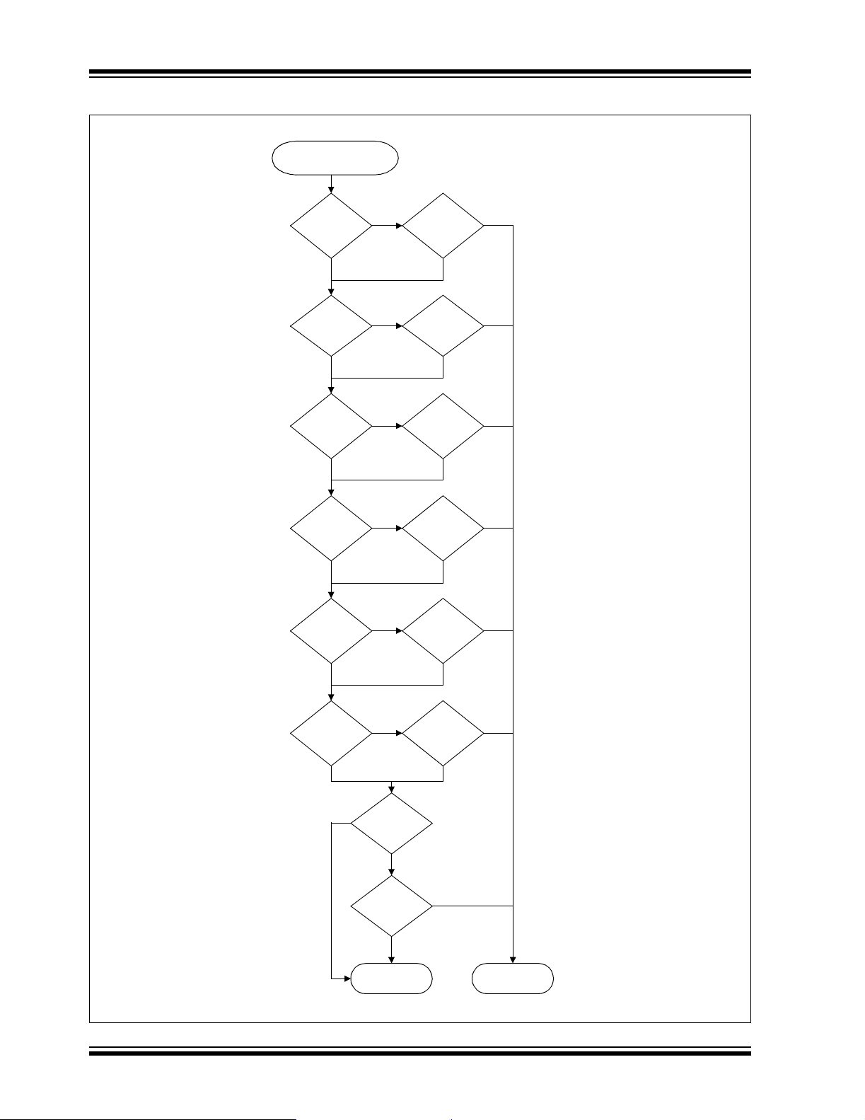
ENC28J60
FIGURE 8-2: RECEIVE FILTERING USING AND LOGIC
Packet Detected on Wire
ANDOR = 1 (AND)
UCEN set?
No
PMEN set?
No Yes
MPEN set?
No Yes
HTEN set?
No Yes
MCEN set?
Yes
Yes
Yes
Yes
Yes
Unicast
packet?
Pattern
matches?
Magic Packet
for us?
Hash table
bit set?
Multicast
destination?
No
Yes
No
No
No
No
No Yes
BCEN set?
No Yes
Yes
No
CRCEN set?
CRC valid?
Accept Packet Reject Packet
destination?
Yes
Yes
Broadcast
No
No
DS39662A-page 50 Advance Information 2004 Microchip Technology Inc.
Page 53
ENC28J60
8.1 Unicast Filter
The unicast receive filter checks the destination
address of all incoming packets. If the destination
address exactly matches the contents of the MAADR
registers, the p acke t will m eet the unic ast fil ter crit eria .
8.2 Pattern Match Filter
The pattern ma tch filt er selects up to 64 by tes from the
incoming packet and calculates an IP checksum of the
bytes. The che cksum is then com pared to the EPMC S
registers. The packet meets the pattern match filter
criteria if the calculated checksum matches the EPMCS
registers. The pattern match filter may be useful for
filtering packets which have expected data ins id e t he m.
To use the pattern match filter, the host controller must
program the pattern m atch offset (E PMOH:EPMOL), all
of the pattern match mask bytes (EPMM7:EPMM0) and
the pattern match checksum resister pair
(EPMCSH:EPMCSL). The pattern match offset should
be loaded with the of fset from th e beginnin g of the destination address field to the 64-byte window which will
be used for the checksum computation. Within the
64-byte window , e ach individ ual byte can be selectiv ely
included or excluded from the checksum computation
by setting or clearing the respective bit in the pattern
match mask. If a p acket i s rec eived which wo uld c ause
the 64 byte window to extend p a st th e e nd of the CRC,
the filter criteria wil l immedi ately not be m et, ev en if th e
corresponding mask bits are all ‘0’. The pattern match
checksum registers should be programmed to the
checksum which is expected for the selected bytes.
The checksum is calculated in the same manner that
the DMA module calculates checksums (see
Section 13.2 “Checksum Calculati ons” ). Data bytes
which have corresp onding mask bi ts programmed to ‘0’
are completely rem oved for pu rposes of calc ulating th e
checksum, as opposed to treating the data bytes as
zero.
As an example, if the application wished to filter all
packets having a particular source MAC address of
00-04-A3-FF-FF-FF, it could p rogram the pattern match
offset to 000 0h and then set bits 6 and 7 of EPMM0 and
bits 0, 1, 2 and 3 of EPMM1 (assuming all other mask
bits are ‘0’). The proper checksum to program into the
EPMCS registers would be 0x5BFC. As an alternative
configuration, it could program the offset to 0006h and
set bits 0, 1, 2, 3, 4 and 5 of EPMM0. The checksum
would still be 5BFCh. However, the second case would
be less desir able as packets less than 70 bytes lo ng
could never meet the pattern match criteria, even if
they would generate the proper checksum given the
mask configuration.
Another example of a pattern matching filter is
illustrated in Figure8-3.
FIGURE 8-3: SAMPLE PATTERN MATCHING FORMAT
Input Configuration:
EMPOH:EPMOL = 0006h
EPPM7:EMPPM0 = 0000000000001F0Ah
EPMCSH:EPMCSL = 563Fh
Field
Received
Data
Bytes used for
Checksum Computation
Values used for Checksum Computation = {88h, AAh, 09h, 0Ah, 0Bh, 0Ch, 0Dh, 00h}
(00h padding byte added by hardware)
Note: Received data is shown in hexadecimal. Byte numbers are shown in decimal format.
11 22 33 44 55 66 77 88 99 AA BB CC
0 1 2 3 4 5 6 7 8 9 10 11 12 13 14 15 16 17 18 . . . 70 . . .Byte #
SA
00 5A
64-Byte Window used
for Pattern Matching
09 0A 0B 0C 0D . . . 40 . . . FE 45 23 01
FCSDA Type/Length Data
2004 Microchip Technology Inc. Advance Information DS39662A-page 51
Page 54
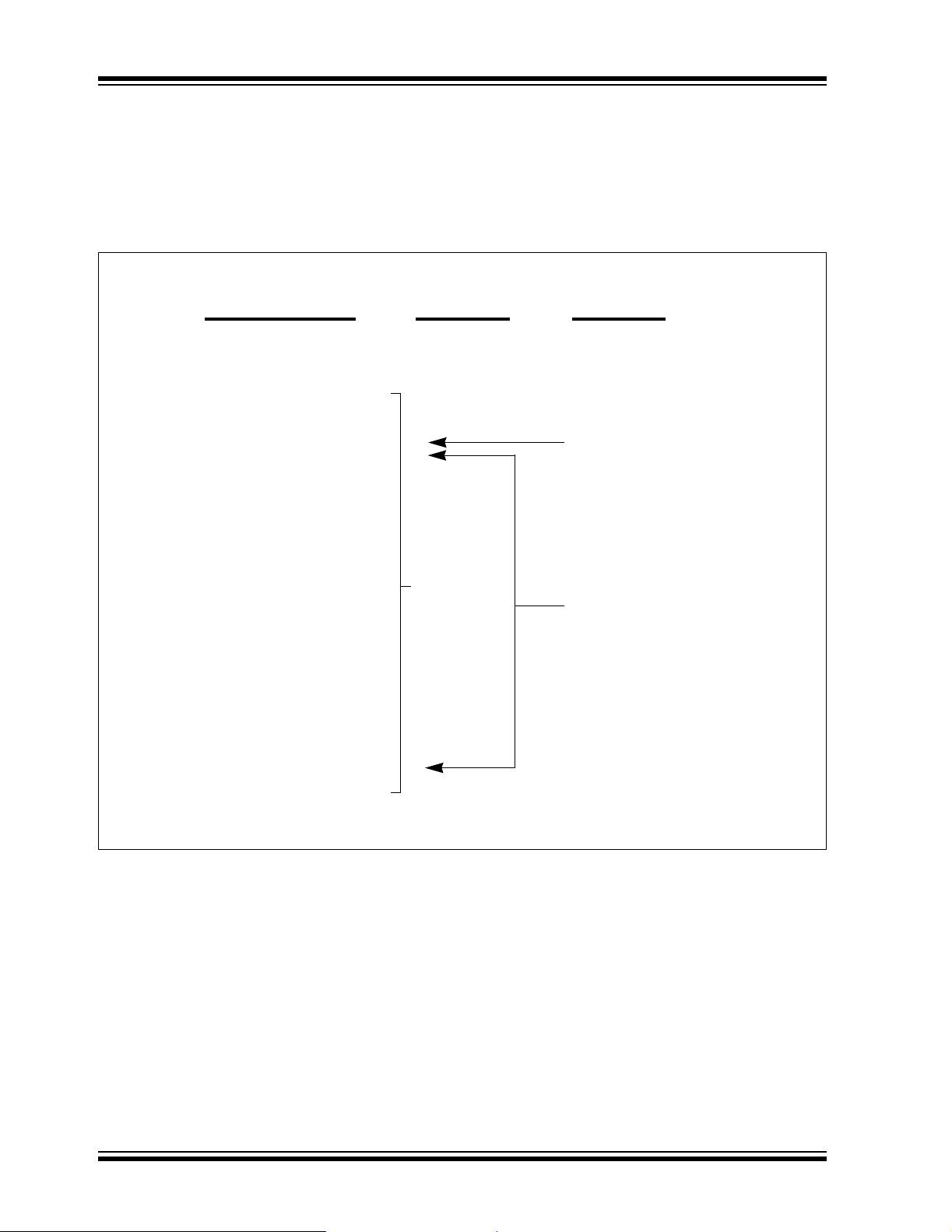
ENC28J60
8.3 Magic Packet™ Filter
The Magic Packet filter checks the destination address
and data fields of all incoming pac kets. If the des tination
address matches the MAADR registers and the data
field holds a valid Magic Packet pattern someplace
FIGURE 8-4: SAMPLE MAGIC PACKET™
Received
Data Field
11 22 33 44 55 66
77 88 99 AA BB CC
00 FE
09 0A 0B 0C 0D 0E
FF FF FF FF FF 00
FF FF FF FF FF FF
11 22 33 44 55 66
11 22 33 44 55 66
11 22 33 44 55 66
11 22 33 44 55 66
11 22 33 44 55 66
11 22 33 44 55 66
11 22 33 44 55 66
11 22 33 44 55 66
11 22 33 44 55 66
11 22 33 44 55 66
11 22 33 44 55 66
11 22 33 44 55 66
11 22 33 44 55 66
11 22 33 44 55 66
11 22 33 44 55 66
11 22 33 44 55 66
19 1A 1B 1C 1D 1E
EF 54 32 10
Type/Length
within it, then the packet will meet the Magic Packet filter
criteria. The Magic Packet pattern consists of a sync
pattern of six 0xFF bytes, followed by 16 repeats of the
destination address. See Figure 8-4 for a sample Magic
Packet.
Comments
DA
SA
Sync Pattern
Data
Data
FCS
Sixteen Repeats of
the Station Address
8.4 Hash Table Filter
The hash table receive filter performs a CRC over the
six destination address bytes in the packet. The CRC is
then used as a pointer int o the bits of the EHT re gisters.
If the pointer points to a bit which is set, the packet
meets the hash table fi lter cri teria. F or exampl e, if t he
CRC is calculated to be 0x5, bit 5 in the hash table will
be checked. If it is set, the hash table filter criteria will
be met. If every bit is clear in the hash table, the filter
criteria will never be met. Similarly, if every bit is set in
the hash table, the filter criteria will always be met.
DS39662A-page 52 Advance Information 2004 Microchip Technology Inc.
8.5 Multicast Filter
The multicast receive filter checks the destination
address of all incomin g packet s. If the Le ast Signifi cant
bit of the first byt e of the destination address is set, th e
packet will meet the multicast filter criteria.
8.6 Broadcast Filter
The broadcast receive filter checks the destination
address of all incoming packets. If the destination
address is FF-FF-FF-FF-FF-FF, the packet will meet
the broadcast filter criteria.
Page 55

ENC28J60
9.0 DUPLEX MODE CONFIGURATION AND NEGOTIATION
The ENC28J60 does not support automatic duplex
negotiation. If it is connected to an automatic duplex
negotiation enable d network switch or Ethernet co ntroller, the ENC28J60 will be detected as a half-duplex
device. To communicate in Full-Duplex mode, the
ENC28J60 and the remote node (switch, router or
Ethernet controller) must be manually configured for
full-duplex operation.
9.1 Half-Duplex Operation
The ENC28J60 operates in Half-Duplex mode when
MACON3.FULDPX = 0 and PHCON1.PDPXMD = 0. If
only one of these two bits is set, the ENC28J60 will be
in an indeterminate state and not function correctly.
Since switching between Full and Half-Duplex modes
may result in this indeterminate state, the host controller should not transmit any packets (maintain
ECON1.TXRTS clear) and packet reception should be
disabled (ECON1.RXEN and ESTAT.RXBUSY should
be clear) during this period.
In Half-Duplex mode, on ly one Ethe rnet cont roll er ma y
be transmi tting on th e phys ical m edium at an y time . If
the host controller sets the ECON1.TXRTS bit,
requesting that a packet be transmitted while another
Ethernet controller is already transmitting, the
ENC28J60 will delay, waiting for the remote transmitter
to stop. After the transmission stops, the ENC28J60
will attempt to transmit its packet. If another Ethernet
controller start s transmi tting at app roximately t he same
time that the ENC28J60 sta rt s trans mittin g, the dat a o n
the wire will become corrupt and a collision will occur.
The hardware will handle this condition in one of two
ways:
1. If the collision occurs befo re the number of bytes
specified by the “Collision Window” in
MACLCON2 were transmitted, the
ECON1.TXRTS bit will remain set, a random
exponential back o ff delay wil l elap se as de fined
by the IEEE 802.3 specification and then a new
attempt to transmit the packet from the beginning will occur. The host controller will not need
to intervene. If the number of retransmission
attempts already matches the “Retransmission
Maximum” (RETMAX) de fined in MACLCON1,
the packet will be aborted and ECON1.TXRTS
will be cleared. The host controller will then be
responsible for taking appropriate action. The
host controller will be able to determine that the
packet was aborted instead of being successfully transmitted by reading the ESTAT.TXABRT
flag. For more information, see Section 7.1
“Transmitting Packets”. A transmit abort will
cause the transmit error interrupt.
2. If the collision occurs after the number of bytes
specified by the “Collision Window” in
MACLCON2 were transmitted, the packet will be
immediately aborted w itho ut any ret ransm issio n
attempts. Ordinarily, in 802.3 compliant
networks which are prope rly configured, this late
collision will not occur. User intervention may be
required to correct the issue. This problem may
occur as a result of a full-duplex node attempting
to transmit on the half-duplex medium. Alternately, the ENC28J60 may be attempting to
operate in Half-Duplex mode while it may be
connected to a full-duplex network. Excessively
long cabling and network size may also be a
possible cause of late coll is ion s.
When set in Half-Duplex mode, the Reset default
configuration will loop transmitted packets back to
itself. Unless t he receive fil ter configurati on filters thes e
packets ou t, they will be written into the ci rcular r eceive
buffer, just as any other network traffic. To stop this
behavior, the host controller should set the
PHCON2.HDLDIS bit.
9.2 Full-Duplex Operation
The ENC28J60 operates in Full-Duplex mode when
MACON3.FULDPX = 1 and PHCON1.PDPXMD = 1. If
only one of these two bits is clear, the ENC28J60 will
be in an indeterminate state and not function correctly.
Since switching between Full and Half-Duplex modes
may result in this indeterminate state, the host controller should not transmit any packets (maintain
ECON1.TXRTS clear) and packet reception should be
disabled (ECON1.RXEN and ESTAT.RXBUSY should
be clear) during this period.
In Full-Duplex mode, packets will be transmitted
simultaneously while packets may be received. Given
this, it is impo ssible to c ause any collisi ons wh en transmitting packets. Several configuration fie lds, such as
“Retransmission Maxi mum” (RETMAX) in MACLCON1
and “Collision Window” (COLWIN) in MACLCON2, will
not be used.
When set in Full-Duplex mode, the Reset default
configuration will not loop transmitted packets back to
itself. If loopbac k is desired for d iagnostic purposes , the
PHCON1.PLOOPBK bit should be set by the host
controller. Enabling loopback in Full-Duplex mode will
disable the twisted pair output driver and ignore all
incoming data, thus dropping any link (if established).
All packets received as a result of the loopback configuration will be subject to all en abl ed rec ei ve fil ters , jus t
as ordinary network traffic would be.
2004 Microchip Technology Inc. Advance Information DS39662A-page 53
Page 56

ENC28J60
NOTES:
DS39662A-page 54 Advance Information 2004 Microchip Technology Inc.
Page 57
ENC28J60
C
B
10.0 FLOW CONTROL
The ENC28J 60 implements hardware flo w control fo r
both Full and Half-D uplex mode s. The o peratio n of this
feature differs depending on which mode is being used.
10.1 Half-Duplex Mode
In Half-Duplex mode, sett ing the EFLO CON.FCEN0 bit
causes flow control to be ena bled. When FCEN0 is set,
a continuous preamble pattern of alternating ‘1’s and
‘0’s (55h) will automatically be transmitted on the
Ethernet medium. Any connected nodes will see the
transmission and either not transmit anything, waiting
for the ENC28J60’s transmission to end, or will att empt
to transmit and immedi ately cau se a coll ision. Bec ause
a collision will always occur, no nodes on the network
will be able to communicate with each other and no
new packets will arrive.
When the host controller tells the ENC28J60 to
transmit a packet by setting ECON1.TXRTS, the
preamble pattern will stop being transmitted. An InterPacket Gap delay will pass as configured by register
MABBIPG and then the ENC28J60 will attempt to
transmit its packet. During the Inter-Packet Gap delay,
other nodes may begin to transmit. Because all traffic
was jammed previously, several nodes may begin
transmitting and a series of collisi ons may occur. When
the ENC28J60 successfully finishes transmitting its
packet or aborts it, the transmission of the preamble
pattern will automatically restart. When the host
controller wishes t o no longer jam th e network, it sh ould
clear the FCEN0 bit. The preamble transmission will
cease and normal network operation will resume.
Given the detrimental network effects that are po ss ibl e
and lack of ef fectivenes s, it is no t recomm end that ha lfduplex flow control be used unless the application will
be in a closed network environmen t with proper tes ting.
10.2 Full-Duplex Mode
matically decrement every 512 bit times or 51.2 µs.
While the timer is counting down, reception of packets
is still enabled. I f new paus e frames arrive , the timer will
be reinitialized with the new pause timer value. When
the timer reaches zero or was sen t a fram e with a ze ro
pause timer value, the MAC that received the pause
frame will resume tran smitting any pend ing pa ckets. To
prevent a pause frame from stopping all traffic on the
entire network, Ethernet switches and routers do not
propagate pause control fr ames in Full -Duplex mode .
The pause operation only applies to the recipient.
A sample network is shown in Figure 10-1. If
Computer A were to be transmitting too much data to
the ENC28J60 in Full-Duplex mode, the ENC28J60
could transmit a pause control frame to stop the data
which is being sent to it. Th e Ethernet switch w ould
take the pause frame and stop sending data to the
ENC28J60. If Computer A continues to send data, the
Ethernet switch will buffer the data so it can be
transmitted later when its pause timer expires. If the
Ethernet switch begins t o run out of buffer space, it will
likely transmit a pause control frame of its own to
Computer A. If, for some reason, the Ethernet switch
does not gene ra t e a pau se co nt ro l f r am e of its own , or
one of the nodes does not properly handle the pause
frame it receives, then packets will inevitably be
dropped. In any event, any communication between
Computer A and Computer B will always be completely
unaffected.
FIGURE 10-1: SAMPLE FULL-DUPLEX
NETWORK
omputer A
Computer
In Full-Duplex mode (MACON3.FULDPX = 1), hardware
flow control is implemented by means of transmitting
pause control frames as defined by the IEEE 802.3
specification. Pause control frames are 64-byte frames
consisting of the reserved multicast destination address
of 01-80-C2-00-00-01, the source address of the sender,
a special pause opcode, a two-byte pause timer value
and padding/CRC.
Normally, when a pause control frame is received by a
MAC, the MAC will finish the packet it is transmitting
and then stop transmitti ng any new frames. The pause
timer value will be ext racted from th e control fram e and
used to initialize an internal timer. The timer will auto-
2004 Microchip Technology Inc. Advance Information DS39662A-page 55
Ethernet Switch
MCP22S80
ENC28J60
Page 58

ENC28J60
To enable flow control on the ENC28J60 in Full-Duplex
mode, the host controller must set the TXPAUS and
RXP AUS bits in the MACON1 register. Then, at any time
that the receiver buffer is running out of space, the host
controller should turn flow control on by writing the v alue
02h to the EFLOCON register . The hardware will periodically transmit pause frames loaded with the pause timer
value specified in the EPAUS registers. The host
controller can continue to transmit its own packets
without interfering with the flow control hardware.
When space has been made available for more packets
in the receive buffer, the host controller should turn flow
control off by writing the value 03h to the EFLOCON
register. The hardware will send one last pause frame
loaded with a pause timer value of 0000h. When the
pause frame is received by the remote node, it will
resume normal netwo rk op erati ons.
When RXPAUS is set in the MACON1 register and a
valid pause frame arrives with a non-zero pause timer
value, the ENC28J60 will automatically inhibit
transmissions. If the host controller sets the
ECON1.TXRTS bit to send a packet, the hardware will
simply wait until the pause timer expires before
attempting to send the packet and subsequently clearing
the TXRTS bit. Normally, the host controller will never
know that a pause frame has been received. However , if
it is desirable to the host controller to know when the
MAC is paused or not, it should set the PASSALL bit in
MACON1 and then manually interpret the pause control
frames which may arrive.
REGISTER 10-1: EFLOCON: ETHERNET FLOW CONTROL REGISTER
U-0 U-0 U-0 U-0 U-0 R-0 R/W-0 R/W-0
— — — — — FULDPXS FCEN1 FCEN0
bit 7 bit 0
bit 7-3 Unimplemented: Read as ‘0’
bit 2 FULDPXS: Read-Only MAC Full-Duplex Shadow bit
1 = MAC is configured for Full-Duplex mode (MACON3.FULDPX is set)
0 = MAC is configured for Half-Duplex mode (MACON3.FULDPX is clear)
bit 1-0 FCEN1:FCEN0: Flow Control Enable bits
When FULDPXS =
11 = Send one pause frame with a ‘0’ timer value and then turn flow control off
10 = Flow control on (pause frames will be automatically transmitted)
01 = Reserved
00 = Flow control off
When FULDPXS =
11 = Flow control on
10 = Flow control off
01 = Flow control on
00 = Flow control off
1:
0:
Legend:
R = Readable bit W = Writable bit U = Unimplemented bit, read as ‘0’
-n = Value at POR ‘1’ = Bit is set ‘0’ = Bit is cleared x = Bit is unknown
DS39662A-page 56 Advance Information 2004 Microchip Technology Inc.
Page 59

ENC28J60
TABLE 10-1: SUMMARY OF REGISTERS USED WITH FLOW CONTROL
Reset
Name Bit 7 Bit 6 Bit 5 Bit 4 Bit 3 Bit 2 Bit 1 Bit 0
ECON1 TXRST RXRST DMAST CSUMEN TXRTS RXEN BSEL1 BSEL0 13
MACON1
MABBIPG — Back-to-Back Inter-Packet Gap (BBIPG<6:0>) 14
EFLOCON — — — — — FULDPXS FCEN1 FCEN0 14
EPAUSL Pause Timer Value Low Byte (EPAUS<7:0>) 14
EPAUSH Pause Timer Value High Byte (EPA US<15:8>) 14
Legend: — = unimplemented, read as ‘0’. Shaded cells are not use d.
— — — LOOPBK TXPAUS RXPAUS PASSALL MARXEN 14
Values
on page
2004 Microchip Technology Inc. Advance Information DS39662A-page 57
Page 60

ENC28J60
NOTES:
DS39662A-page 58 Advance Information 2004 Microchip Technology Inc.
Page 61

11.0 RESET
The ENC28J60 dif f eren tia tes between various kinds of
Reset:
• Power-on Reset (PO R)
• System Reset
• Transmit Only Reset
• Receive Only Reset
• Miscellaneous MAC and PHY Subsystem Resets
A simplified b lock di agram of the On -Chip Re set Ci rcuit
is shown in Figure11-1.
FIGURE 11-1: ON-CHIP RESET CIRCUIT
Soft Reset Command
Hardware Reset
ENC28J60
POR
Transmit Reset
Receive Reset
System Reset
Reset Host Interface
Reset Transmit
Reset Receive
2004 Microchip Technology Inc. Advance Information DS39662A-page 59
Page 62

ENC28J60
11. 1 Power-on Reset (POR)
A Power-on Reset pulse is generated on-chip
whenever V
allows the device to start in the initialized state when
VDD is adequate for operation.
The POR circuitry is always enabled. As a result, most
applications do n ot need to att ach a ny exter nal circuit ry
to the RESET
up. The RESET
a logical high level on the pin during normal device
operation.
To ensure proper POR operation, a minimum rise rate
for V
circuit must meet this requirement to allow the Oscillator
Start-up Timer and CLKOUT functions to reset properly.
After a Power -on Reset, the contents of t he dual port
buffer memory will be unkn ow n. Howe ver, all regi ster s
will be loaded with their speci fied Reset values . Certain
portions of the ENC28J60 must not be accessed
immediately after a POR. See Section 2.2 “Oscillator
Start-up Timer” for more information.
DD rises above a certain threshold. This
pin to ensure a proper Reset at power-
pin’s intern al weak pull -up will main tain
DD is specified (parameter D004). The application
11.2 System Reset
The System Reset o f EN C28J 60 can be accomplished
by either the RESET
The RESET
triggering an external Reset of the device. A Reset is
generated by holding the RESET pin low. The
ENC28J60 has a noise filter in the RESET
detects and ignore s small pulses. When the RESET
is held high, the ENC28J60 will operate normally.
The ENC28J60 can also be reset via the SPI using a
system command. See Section 4.0 “Serial Peripheral
Interface (SPI)”.
The RESET
Resets, including the System Command Reset via the
SPI interface.
pin provides an asynchronous method for
pin will no t be driven lo w by any inte rnal
pin, or through the SPI interface.
path wh i c h
pin
After a System Reset, all PHY registers should not be
read or written to until a t least 50 µs have passed since
the Reset has ended. All registers will revert to their
Reset def a ul t va l ue s. T he du a l po rt bu ffe r m emory will
maintain state throughout the System Reset.
11.3 Transmit Only Reset
The Transmit Only Reset is performed by writing a ‘1’ to
the TXRST bit in the ECON1 register using the SPI interface. If a packet was being transmitted when the TXRST
bit was set, the hardware will automatically clear the
TXRTS bit and abort the transmission. This action reset s
the transmit logic only. The System Reset automatically
performs the Transmit Only Reset. Other register and
control blocks, such as buffer management and host
interface, are not affected by a Transmit Only Reset
event. When the host controller wishes to return to
normal operation, it should clear the TXRST bit.
11. 4 Receive Only Reset
The Receive Only Reset is performed by writ ing a ‘ 1’ to
the RXRST bit in the ECON1 register using the SPI
interface. If packet reception was enabled (the RXEN
bit was set) when RXRST was set, the hardware will
automatically cle ar the RXEN bit. If a p ack et was bein g
received, it would be immediately aborted. This action
resets receiv e lo gic onl y. The System Rese t au to mati cally performs Receive Only Reset. Other register and
control blocks, such as the buffer management and
host interface blocks, are not affected by a Receive
Only Reset event. When the host controller wishes to
return to normal operation, it should clear the RXRST
bit.
DS39662A-page 60 Advance Information 2004 Microchip Technology Inc.
Page 63

ENC28J60
11.5 MAC and PHY Subsystem Resets
The PHY module may be reset by writing a ‘1’ to the
PRST bit in the PHCON1 register. All the PHY register
contents will rev ert to their Reset defaults. Unlike oth er
Resets, the PHY cann ot be removed from Reset immediately after setting PRST. The PHY requires a delay,
after which the hardware automatically clears the
PRST bit. The host controller should poll PRST and
wait for it to become clear before using the PHY after
issuing a Reset. The System Reset automatically
performs this PHY Reset.
There are a total of nine Resets available to the MAC
subsystem. Six Reset bits are found in the MACON2
register:
• MARST
• RNDRST
• MARXRST
• RFUNRST
• MATXRST
• TFUNRST
There are also two Reset bits loc ated in the MAPHSUP
register (RSTINTFC and R ST R MII ) and one in MICON
(RSTMII). Setting any of these bits will cause some
portion of the ENC28J60 to stop funct ioning prope rly. It
is recommended that all bits be kept clear.
A System Reset automatically performs all of these
Subsystem Resets. However, after a System Reset,
the global MAC Reset bit, MARST, remains set. The
host controller must clear this bit before attempting to
transmit packets, receive packets or access any PHY
register.
The MAC and PHY Reset bits are explained in
Register 11-1, Register 11-2 and Register 11-3. The
RSTMII bit is shown in Register 3-3 (page 21).
REGISTER 11-1: MACON2: MAC CONTROL REGISTER 2
R/W-1 R/W-0 U-0 U-0 R/W-0 R/W-0 R/W-0 R/W-0
MARST RNDRST — — MARXRST RFUNRST MATXRST TFUNRST
bit 7 bit 0
bit 7 MARST: MAC Reset bit
1 = Entire MAC is held in Reset
0 = Normal operation
bit 6 RNDRST: MAC Random Number Generator Reset bit
1 = Random number generator used in transmit function is held in Reset
0 = Normal operation
bit 5-4 Unimplemented: Read as ‘0’
bit 3 MARXRST: MAC Control Sublayer/Receive Logic Reset bit
1 = MAC control sublayer and receiver logic are held in Reset
0 = Normal operation
bit 2 RFUNRST: MAC Receive Function Reset bit
1 = MAC receive logic is held in Reset
0 = Normal operation
bit 1 MATXRST: MAC Control Sublayer/Transmit Logic Reset bit
1 = MAC control sublayer and transmit logic are held in Reset
0 = Normal operation
bit 0 TFUNRST: MAC Transmit Function Reset bit
1 = MAC transmit logic is held in Reset
0 = Normal operation
Legend:
R = Readable bit W = Writable bit U = Unimplemented bit, read as ‘0’
-n = Value at POR ‘1’ = Bit is set ‘0’ = Bit is cleared x = Bit is unknown
2004 Microchip Technology Inc. Advance Information DS39662A-page 61
Page 64

ENC28J60
REGISTER 11-2: MAPHSUP: MAC-PHY SUPPORT REGISTER
R/W-0 U-0 U-0 R/W-1 R/W-0 U-0 U-0 R/W-0
RSTINTFC — —rRSTRMII— —r
bit 7 bit 0
bit 7 RSTINTFC: Interface Module Reset bit
1 = RMII module is held in Reset
0 = Normal operation if RSTRMII is also cleared
bit 6-5 Unimplemented: Read as ‘0’
bit 4 Reserved: Maintain as ‘1’
bit 3 RSTRMII: RMII Module Reset bit
1 = RMII module is held in Reset
0 = Normal operation if RSTINTFC is also cleared
bit 2-1 Unimplemented: Read as ‘0’
bit 0 Reserved: Maintain as ‘0’
Legend:
R = Readable bit W = Writable bit U = Unimplemented bit, read as ‘0’
-n = Value at POR ‘1’ = Bit is set ‘0’ = Bit is cleared x = Bit is unknown
DS39662A-page 62 Advance Information 2004 Microchip Technology Inc.
Page 65

ENC28J60
REGISTER 11-3: PHCON1: PHY CONTROL REGISTER 1
R/W-0 R/W-0 U-0 U-0 R-1 R/W-0 U-0 R-x
PRST PLOOPBK — — PPWRSV r — PDPXMD
bit 15 bit 8
R/W-0 U-0 U-0 U-0 U-0 U-0 U-0 U-0
r
bit 7 bit 0
bit 15 PRST: PHY Software Reset bit
1 = PHY is processing a Software Reset (automatically resets to ‘0’ when done)
0 = Normal operation
bit 14 PLOOPBK: PHY Loopback bit
1 = All data transmitted will be returned to the MAC. The twisted pair interface will be disabled.
0 = Normal operation
bit 13-12 Unimplemented: Read as ‘0’
bit 11 PPWRSV: PHY Power-Down bit
1 = PHY is shut-down
0 = Normal operation
bit 10 Reserved: Maintain as ‘0’
bit 9 Unimplemented: Read as ‘0’
bit 8 PDPXMD: PHY Duplex Mode bit
1 = PHY operates in Full-Duplex mode
0 = PHY operates in Half-Duplex mode
Note 1: The Reset default of PDPXMD depends on the external polarity of the LEDB LED.
bit 7 Reserved: Maintain as ‘0’
bit 6-0 Unimplemented: Read as ‘0’
— — — — — — —
(1)
(1)
Legend:
R = Readable bit W = Writable bit U = Unimplemented bit, read as ‘0’
-n = Value at POR ‘1’ = Bit is set ‘0’ = Bit is cleared x = Bit is unknown
2004 Microchip Technology Inc. Advance Information DS39662A-page 63
Page 66

ENC28J60
NOTES:
DS39662A-page 64 Advance Information 2004 Microchip Technology Inc.
Page 67

ENC28J60
12.0 INTERRUPTS
The ENC28J60 has multiple interrupt sources and two
separate interrupt output pins to signal the occurrence
of events to the host controller. The interrupt pins are
designed for use by a host controller which is capable
of detecting falling edges.
Interrupts are divided into two sources: control events
(INT) and Wak e-up on LAN (WOL) even ts. The EIE and
EWOLIE registers contain the individual interrupt
enable bits for each int errupt sourc e, while the EIR and
EWOLIR registers contain the corresponding interrupt
flag bits. When an interrupt occurs, the interrupt flag is
set. If the interrupt is enabled in the EIE or EWOLIE
registers and the corresponding IN TIE or WOLIE globa l
interrupt enable bit is set, the appropriate INT
interrupt pin will be driven low by the ENC28J60 (see
Figure 12-1).
Note: Except for the LINKIF interrupt flag,
interrupt flag bits are set when an interrupt
condition occurs regardless of the state of
its corresponding enable bit or the associated global enable bit. User software
should ensure the appropriate interrupt flag
bits are clear prior to enabling an interrupt.
This feature allows for software polling.
or WOL
When an enabled i nte rrupt occurs, the interrupt pin wil l
remain low until al l flags which are causing the interrupt
are cleared or maske d off (enable bit is cleared) by the
host controller. If more than one interrupt source is
enabled, the host controller must poll each flag in the
EIR or EWOLIR register to determine the source(s) of
the interrupt. It is rec ommend ed that the Bi t Field Clear
(BFC) SPI command be use d to reset the fl ag bits in the
EIR and EWOLIR registers rather than the normal
Write Control Register (WCR) command. This is
necessary to prevent uni ntenti onally alterin g a flag th at
changes during the write command. The BFC and
WCR commands are disc ussed in detai l in Section 4.0
“Serial Peripheral Interface (SPI)”.
After an interrupt occurs, the host controller should
clear the global enable bit for the interrupt pin before
servicing the interrupt. Clearing the enable bit will
cause the interrupt pin to return to the non-asserted
state (high). Doing so will prevent the host controller
from missing a falling edge should another interrupt
occur while the immediate interrupt is being serviced.
After the interrupt has been se rviced, the glob al enable
bit may be restored. If an in terrupt event occurre d while
the previous interrupt was being processed, the act of
resetting the gl obal enab le bit will ca use a ne w falli ng
edge on the interrupt pin to occur.
FIGURE 12-1: ENC28J60 INTERRUPT LOGIC
PKTIF
PKTIE
DMAIF
PLNKIF
PLNKIE
PGIF
PGEIE
LINKIF
DMAIE
LINKIE
TXIF
TXIE
TXERIF
TXERIE
RXERIF
RXERIE
UCWOLIF
UCWOLIE
AWOLIF
AWOLIE
PMWOLIF
PMWOLIE
MPWOLIF
MPWOLIE
HTWOLIF
HTWOLIE
MCWOLIF
MCWOLIE
BCWOLIF
BCWOLIE
INT
INT
INTIE
WOLIF
WOL
WOLIE
2004 Microchip Technology Inc. Advance Information DS39662A-page 65
Page 68

ENC28J60
12.1 INT Interrupt Enable (INTIE)
The INT Interrupt Enable bit (INTIE) is a global enable
bit which allows the follo wing interrupt s to drive the INT
pin:
• Receive Error Interrupt (RXERIF)
• Transmit Error Interrupt (TXERIF)
• Transmit Interrupt (TXIF)
• Link Change Interrupt (LINKIF)
• DMA Interrupt (DMAIF)
• Receive Packet Pending Interrupt (PKTIF)
When any of the above interrupts are enabled and
generated, the virtual bit, INT in the ESTAT register
(Register 12-1), will be set to ‘1’. If EIE. INTIE i s ‘1’, th e
pin will be d riven low.
INT
12.1.1 INT INTERRUPT REGISTERS
The registers associated with the INT interrupts are
shown in Register 12-2, Register 12-3, Register 12-4
and Register 12-5.
REGISTER 12-1: ESTAT: ETHERNET STATUS REGISTER
R-0 R/C-0 R-0 R/C-0 U-0 R-0 R/C-0 R/W-0
INT r r LATECOL — RXBUSY TXABRT CLKRDY
bit 7 bit 0
bit 7 INT: INT Interrupt Flag bit
1 = INT interrupt is pending
0 = No INT interrupt is pending
bit 6-5 Reserved: Maintain as ‘0’
bit 4 LATECOL: Late Collision Error bit
1 = A collision occurred after 64 bytes have been transmitted
0 = No collisions after 64 bytes have occurred
bit 3 Unimplemented: Read as ‘0’
bit 2 RXBUSY: Receive Busy bi t
1 = Receive logic is receiving a data packet
0 = Receive logic is Idle
bit 1 TXABRT: Transmit Abort Error bit
1 = The transmit request was aborted
0 = No transmit abort error
bit 0 CLKRDY: Clock Ready bit
1 = OST has expired; PHY is ready
0 = OST is still counting; PHY is not ready
Legend:
R = Readable bit C = Clearable bit U = Unimplemented bit, read as ‘0’
-n = Value at POR ‘1’ = Bit is set ‘0’ = Bit is cleared r = Reserved bit
DS39662A-page 66 Advance Information 2004 Microchip Technology Inc.
Page 69

REGISTER 12-2: EIE: ETHERNET INTERRUPT ENABLE REGISTER
R/W-0 R/W-0 R/W-0 R/W-0 R/W-0 R/W-0 R/W-0 R/W-0
INTIE PKTIE DMAIE LINKIE TXIE WOLIE TXERIE RXERIE
bit 7 bit 0
bit 7 INTIE: Global INT Interrupt Enable bit
1 = Allow interrupt events to drive the INT
0 = Disable all INT
bit 6 PKTIE: Receive Packet Pending Interrupt Enable bit
1 = Enable receive packet pending interrupt
0 = Disable receive packet pending interrupt
bit 5 DMAIE: DMA Interrupt Enable bit
1 = Enable DMA interrupt
0 = Disable DMA interrupt
bit 4 LINKIE: Link Status Change Interrupt Enable bit
1 = Enable link change interrupt from the PHY
0 = Disable link change interrupt
bit 3 TXIE: Transmit Enable bit
1 = Enable transmit interrupt
0 = Disable transmit interrupt
bit 2 WOLIE: Global WOL Interrupt Enabl e bit
1 = Allow WOL interrupt events to drive the WOL pin
0 = Disable all WOL
bit 1 TXERIE: Transmit Error Interrupt Enable bit
1 = Enable transmit error interrupt
0 = Disable transmit error interrupt
bit 0 RXERIE: Receive Error Interrupt Enable bit
1 = Enable receive error interrupt
0 = Disable receive error interrupt
pin activity (pin is continuously driven high)
pin activity (pin is continuously driven high)
pin
ENC28J60
Legend:
R = Readable bit W = Writable bit U = Unimplemented bit, read as ‘0’
-n = Value at POR ‘1’ = Bit is set ‘0’ = Bit is cleared x = Bit is unknown
2004 Microchip Technology Inc. Advance Information DS39662A-page 67
Page 70

ENC28J60
REGISTER 12-3: EIR: ETHERNET INTERRUPT REQUEST (FLAG) REGISTER
U-0 R-0 R/C-0 R-0 R/C-0 R-0 R/C-0 R/C-0
— PKTIF DMAIF LINKIF TXIF WOLIF TXERIF RXERIF
bit 7 bit 0
bit 7 Unimplemented: Read as ‘0’
bit 6 PKTIF: Receive Packet Pending Interrupt Flag bit
1 = Receive buffer contains one or more unprocessed packets; cleared when PKTDEC is set
0 = Receive bu ffer is empty
bit 5 DMAIF: DMA Interrupt Flag bit
1 = DMA copy or checksum calculation has completed
0 = No DMA interrupt is pending
bit 4 LINKIF: Link Change Interrupt Flag bit
1 = PHY reports that the link status has changed; read PHIR register to clear
0 = Link status has not changed
bit 3 TXIF: Transmit Interrupt Flag bit
1 = Transmit request has ended
0 = No transmit interrupt is pending
bit 2 WOLIF: WOL Interrupt Flag bit
1 = Wake-up on LAN interrupt is pending
0 = No Wake-up on LAN interrupt is pending
bit 1 TXERIF: Transmit Error Interrupt Flag bit
1 = A transmit error has occurred
0 = No transmit error has occurred
bit 0 RXERIF: Receive Error Interrupt Flag bit
1 = A packet was aborted becau se there is insuf fic ient bu ff er sp ace or the pa cket coun t is 255
0 = No receive error interrupt is pending
Legend:
R = Readable bit C = Clearable bit U = Unimplemented bit, read as ‘0’
-n = Value at POR ‘1’ = Bit is set ‘0’ = Bit is cleared x = Bit is unknown
DS39662A-page 68 Advance Information 2004 Microchip Technology Inc.
Page 71

ENC28J60
REGISTER 12-4: PHIE: PHY INTERRUPT ENABLE REGISTER
R/W-x R/W-x R/W-x R/W-x R/W-x R/W-x R/W-x R/W-x
rrrr rrrr
bit 15 bit 8
R/W-x R/W-x R/W-0 R/W-0 R/W-x R/W-x R/W-0 R/W-0
rrrPLNKIErrPGEIEr
bit 7 bit 0
bit 15-6 Reserved: Write as ‘0’, ignore on read
bit 5 Reserved: Maintain as ‘0’
bit 4 PLNKIE: PHY Link Change Interrupt Enable bit
1 = PHY link change interrupt is enabled
0 = PHY link change interrupt is disabled
bit 3-2 Reserved: Write as ‘0’, ignore on read
bit 1 PGEIE: PHY Global Interrupt Enable bit
1 = PHY interrupts are enabled
0 = PHY interrupts are disabled
bit 0 Reserved: Maintain as ‘0’
Legend:
R = Readable bit W = Writable bit r = Reserved bit U = Unimplemented bit, read as ‘0’
-n = Value at POR ‘1’ = Bit is set ‘0’ = Bit is cleared x = Bit is unknown
REGISTER 12-5: PHIR: PHY INTERRUPT REQUEST (FLAG) REGISTER
R-x R-x R-x R-x R-x R-x R-x R-x
rrrr rrrr
bit 15 bit 8
R-x R-x R-0 R/SC-0 R-0 R/SC-0 R-x R-0
r r r PLNKIF r PGIF r r
bit 7 bit 0
bit 15-5 Reserved
bit 4 PLNKIF: PHY Link Change Interrupt Flag bit
1 = PHY link status has changed since PHIR was last read; resets to ‘0’ when read
0 = PHY link status has not changed since PHIR was last read
bit 3 Reserved
bit 2 PGIF: PHY Global Interrupt Flag bit
1 = One or more enabled PHY interrupts have occurred since PHIR was last read; resets to ‘0’ when read
0 = No PHY interrupts have occurred
bit 1-0 Reserved
Legend:
R = Readable bit SC = Self-clearing bit U = Unimplemented bit, read as ‘0’
r = Reserved bit ‘1’ = Bit is set on POR ‘0’ = Bit is cleared on POR x = Bit is unknown
2004 Microchip Technology Inc. Advance Information DS39662A-page 69
Page 72

ENC28J60
12.1.2 RECEIVE ERROR INTERRUPT FLAG (RXERIF)
The Receive Error Interrupt Flag (RXERIF) is used to
indicate a receive buffer ov erflow con dition. Altern ately ,
this interrupt may i ndi cate that too many packe t s are in
the receive buffer and more cannot be stored without
overflowing the EPKTCNT register.
When a packet is b eing recei ved and the receive buf fer
runs completely out of space, or EPKTCNT is 255 and
cannot be incremented, the packet being received will
be aborted (permanently lost) and the EIR.RXERIF bit
will be set to ‘1’. Once se t, RXERIF can only be cleared
by the host controller or by a Reset condition. If the
receive error interrupt and INT interrupt are enabled
(EIE.RXERIE = 1 and EIE.INTIE = 1), an interrupt is
generated by driving the INT
interrupt is not enabled (EIE.RXERIE = 0 or EIE.INTIE
= 0), the host co ntrol le r m ay po ll the EN C28 J6 0 fo r th e
RXERIF and take appropriate action.
Normally, upon the receive error condition, the host
controller would proces s any p acke ts pen ding from the
receive buffer and then make additional room for future
packets by advancing the ERXRDPT registers (low
byte first) and decrementing the EPKTCNT register.
See Section 7.2.4 “Freeing Receive Buffer Space”
for more information on processing packets. Once
processed, the host controller should use the BFC
command to clear the EIR.RXERIF bit.
pin low. If the receive error
12.1.3 TRANSMIT ERROR INTERRUPT FLAG (TXERIF)
The Transmit Error Interrupt Flag (TXERIF) is used to
indicate that a transmit abort has occurred. An abort
can occur because of any of the following:
1. Excessive collisions occurred as defined by the
Retransmission Maximum (RETMAX) bits in the
MACLCON1 register.
2. A late collision occurred as defined by the
Collision Window (COLWIN) bits in the
MACLCON2 register.
3. A collision after transmitting 64 bytes occurred
(ESTAT.LATECOL set).
4. The transmission was unable to gain an
opportunity to transmit the packet because the
medium was c onstantly occupied f or too long.
The deferral limit (2.4287 ms) was reached and
the MACON4.DEFER bit was clear.
5. An attempt to transmit a packet larger than the
maximum frame length d efined by the M AMXFL
registers was made without setting the
MACON3.HFRMEN bit or per packet
POVERRIDE and PHUGEEN bits.
Upon any of th ese con ditions , the EI R.TXERIF flag i s set
to ‘1’. Once set, it can only be cleared by the host
controller or by a Res et condition. If the transm it error
interrupt is enabled (EIE. TXERIE = 1 and EIE.INT IE = 1),
an interrup t is generated by dr iving the INT
one OSC1 period. If the transmit error interrupt is not
enabled (EIE. TXERIE = 0 or EIE.INTIE = 0), th e host
controller may poll the ENC28J60 for the TXERIF and
take appropriate action. Once the interrupt is processed,
the host con troller s hould use t he BFC c ommand to clear
the EIR.TXERIF bit.
After a transmit abort, the TXRTS bi t will be cleared, th e
ESTAT.TXABRT bit will be set and the transmit status
vector will be written at ETXND + 1. The MAC will not
automatically attempt to retransmit the packet. The
host controller may wish to read the transmit status
vector and LATECOL bit to determine the cause of the
abort. After determining the problem and solution, the
host controller should clear the LATECOL (if set) and
TXABRT bits so that future aborts can be detected
accurately.
In Full-Duplex mode, condition 5 is the only one that
should cause this interrupt. Collisions and other problems related to sharing the netwo rk are not possibl e on
full-duplex networks. The conditions which cause the
transmit error interrupt meet the requirements of the
transmit interrupt. As a result, when this interrupt
occurs, TXIF will also be simultaneously set.
pin low for
12.1.4 TRANSMIT INTERRUPT FLAG (TXIF)
The Transmit Interrupt Flag (TXIF) is used to indicate
that the requested packet transmission has ended
(ECON1.TXRTS has transitioned from ‘1’ to ‘0’). Upon
transmission completion, abort or transmission cancellation by the host controller , the EIR.TXIF flag will be set to
‘1’. If the host controller did not clear the TXRTS bit and
the ESTAT.TXABRT bit is not set, then the packet was
successfully transmitted. Once TXIF is set, it can only be
cleared by the host controller or by a Reset condition. If
the transmit interrupt is enabled (EIE.TXIE = 1 and
EIE.INTIE = 1), an interrupt is generated by driving the
pin low. If the transmit interrupt is not enabled
INT
(EIE.TXIE = 0 or EIE.INTIE = 0), the host controller may
poll the ENC28J60 for the TXIF bit and take appropriate
action. Once processed, the host controller should use
the BFC command to clear the EIR.TXIF bit.
DS39662A-page 70 Advance Information 2004 Microchip Technology Inc.
Page 73

ENC28J60
12.1.5 LINK CHANGE INTERRUPT FLAG (LINKIF)
The LINKIF indicates t hat the link status has changed.
The actual current lin k status can be obtained from th e
PHSTA T1.LLST A T or PHST A T2.LST A T (see Register 3-6
and Register 3-7). Unlike other interrupt sources, the link
status change interrupt is creat ed in the i ntegrated P HY
module; additional steps must be taken to enable it.
By Reset default, LINKIF is never set for any reason. To
receive it, the host controller must set the
PHIE.PLNKIE and PGEIE bits. After setting the two
PHY interrupt enable bits, the LINKIF bit will then
shadow the contents of the PHIR.PGIF bit. The PHY
only supports one interrupt, so the PGIF bit will always
be the same as the PHIR.PLNKIF bit (when both PHY
enable bits are set).
Once LINKIF is set, it can only be cleared by the host
controller or by a Reset. If the link change interrupt
is enabled (EIE.LINKIE = 1, EIE.INTIE = 1,
PHIE.PLNKIE = 1 and PHIE.PGEIE = 1), an interrupt
will be generated by driving the INT
change interrupt is not enabled (EIE.LINKIE = 0,
EIE.INTIE = 0, PHIE.PLNKIE = 0 or PHIE.PGEIE = 0),
the host controller may poll the ENC28J60 for the
PHIR.PLNKIF bit and take appropriate action.
The LINKIF bit is read-only. Because reading from PHY
registers requires non-negligible time, the host controller
may instead set PHIE.PLNKIE and PHIE.PGEIE and
then poll the EIR.LINKIF bit. Performing an MII read on
the PHIR register will clear the LINKIF, PGIF and
PLNKIF bits automatically and allow for future link status
change interrupts. See Section 3.3 “PHY Registers”
for information on accessing the PHY registers.
pin low. If the link
12.1.6 DMA INTERRUPT FLAG (DMAIF)
The DMA interrupt indicates that the DMA module has
completed its memory copy or checksum calculation
(ECON1.DMAST has transitioned from ‘1’ to ‘0’). Additionally, this interrupt will be caused if the host controller
cancels a DMA operation by manually clearing the
DMAST bit. Once set, DMAIF can only be cleared by the
host controller or by a Reset condition. If the DMA
interrupt is enabled (EIE.DMAIE = 1 and EIE.INTIE = 1),
an interrupt is generated by driving the INT
DMA interrupt is not enabled (EIE.DMAIE = 0 or
EIE.INTIE = 0), the host controller may poll the
ENC28J60 for the DMAIF and take appropriate action.
Once processed, the host controller should use the BFC
command to clear the EIR.DMAIF bit.
pin low. If the
12.1.7 RECEIVE PACKET PENDING INTERRUPT FLAG (PKTIF)
The Receive Packet Pending Interrupt Flag (PKTIF) is
used to indicate the presence of one or more data p ackets in the receive buffer and to provide a notification
means for the arrival of new packets. When the receive
buffer has at least one packet in it, EIR.PKTIF will be set.
In other words, this interrupt flag will be set anytime the
Ethernet Packet Count register (EPKTCNT) is non-zero.
If the receive packet pending interrupt is enabled
(EIE.PKTIE = 1 and EIE.INTIE = 1), an interrupt will be
generated by driving the INT
packet is successfully received and written into the
receive buffer. If the receive packet pending interrupt is
not enabled (EIE.PKTIE = 0 or EIE.INTIE = 0), the host
controller will not be notified when new packets arrive.
However, it may poll the PKTIF bit and take appropriate
action.
The PKTIF bit can only be cleared by the hos t controller
or by a Reset condition. In order to clear PKTIF, the
EPKTCNT register must be decremented to ‘0’. See
Section 7.2 “Receiving Packets” for more information about clearing the EPKTCNT register. If the last
data packet in the receive buffer is processed,
EPKTCNT will become zero and the PKTIF bit will
automatically be cleared.
pin low whenever a new
12.2 Wake-up on LAN Interrupt
(WOLIE/WOLIF)
The WOL interrupt is designed to cause a wake-up
event for the host controller. The WOL interrupt is a
multisource interrupt and controls the WOL
pin. WOL interrupts are not affected by the EIE.INTIE
configuration.
There are a t ota l of s ev en d i ffere n t co ndi t io ns t hat c an
cause this interrupt. The EWOLI E bits allow the indi vidual conditions to be enab led. If mul tiple bit s are set, any
of the enabl ed conditions will be able to generate the
WOL interrupt. However, the WOL filter logic is applied
after the receive filter logic. As a result, any packet
which is rejected as a result of the receiv e filter c onfiguration (see Section8.0 “Receive Filters”) will not be
able to cause a WOL interrupt.
interrupt
2004 Microchip Technology Inc. Advance Information DS39662A-page 71
Page 74

ENC28J60
When any of the seven WOL conditions are detected,
the associated interrupt flag in the EWO LIR register will
be set. If the associated interrupt enable is set in
EWOLIE, then the EIR.WOLIF bit w ill also becom e set.
If the global WOL interrupt enable bit is set
(EIR.WOLIF), then an interrupt will be generated by
driving the WOL
enabled (EIE.WOLIE = 0 or the associated bit in
EWOLIE = 0), the host controll er may poll the EWOLIR
register and take appropriate action when the desired
flag becomes se t. N o rma lly, upon recei vi ng the WOLIF
interrupt, the host controller would come out of Sleep
and check the EWOLI R register for the ac tual source(s)
of the interrupt. Depending on the application requirements, the host controller may either disable further
WOLIF interrupts or keep it enabled and go back to
Sleep. Once the interrupt is processed, the host
controller should use the BFC command to clear the
EIR.WOLIF bit and associated EWOLIR bits.
pin low. If the WOL interrupt is not
Note: When using the WOL interrupt, care
should be taken to prevent the receive
buffer from filling up without waking the
host controller. If the receive buffer
becomes full, without meeting any of the
WOL criteria, a ll addi tional inco ming p ackets will be aborted. Aborted packets are
not able to cause the WOL
if they meet the configured criteria. As a
result, the WOL
generated.
interrupt w ould never be
interrupt, even
12.2.1 WOL INTERRUPT REGISTERS
The registers associated with the WOL interrupts are
shown in Re gister 12-6 and Register 12-7. The interrupt flag bits a re set when an interrup t cond ition occur s
regardless of the state of its corresponding enable bit.
This feature allows for software polling.
REGISTER 12-6: EWOLIE: ETHERNET WAKE-UP ON LAN INTERRUPT ENABLE REGISTER
R/W-0 R/W-0 U-0 R/W-0 R/W-0 R/W-0 R/W-0 R/W-0
UCWOLIE AWOLIE — PMWOLIE MPWOLIE HTWOLIE MCWOLIE BCWOLIE
bit 7 bit 0
bit 7 UCWOLIE: Unicast Wake-up on LAN Interrupt Enable bit
1 = Enable Unicast Wake-up on LAN interrupt
0 = Disable Unicast Wake-up on LAN interrupt
bit 6 AWOLIE: Any Packet Wake-up on LAN Interrupt Enable bit
1 = Enable Any Packet Wake-up on LAN interrupt
0 = Disable Any Packet Wake-up on LAN interrupt
bit 5 Unimplemented: Read as ‘0’
bit 4 PMWOLIE: Pattern Match Wake-up on LAN Interrupt Enable bit
1 = Enable Pattern Match Wak e-up on LAN inte rrupt
0 = Disable Pattern Match Wake-up on LAN interrupt
bit 3 MPWOLIE: Magic Packet Wake-up on LAN Interrupt Enable bit
1 = Enable Magic Packet Wake-up on LAN interrupt
0 = Disable Magic Packet Wake-up on LAN interrupt
bit 2 HTWOLIE: Hash Table Wake- up on LAN Interrupt Enable bit
1 = Enable Hash Table Wake-up on LAN interrupt
0 = Disable Hash Table Wake-up on LAN interrupt
bit 1 MCWOLIE: Multicast Packet Wake-up on LAN Interrupt Enable bit
1 = Enable Mulitcast Packet Wake-up on LAN interrupt
0 = Disable Multicast Packet Wake-up on LAN interrupt
bit 0 BCWOLIE: Broadcast Packet Wake-up on LAN Interrupt Enable bit
1 = Enable Broadcast Packet Wake-up on LAN interrupt
0 = Disable Broadcast Packet Wake-up on LAN interrupt
Legend:
R = Readable bit W = Writable bit U = Unimplemented bit, read as ‘0’
-n = Value at POR ‘1’ = Bit is set ‘0’ = Bit is cleared x = Bit is unknown
DS39662A-page 72 Advance Information 2004 Microchip Technology Inc.
Page 75

ENC28J60
REGISTER 12-7: EWOLIR: ETHERNET WAKE-UP ON LAN INTERRUPT REQUEST
(FLAG) REGISTER
R/C-0 R/C-0 U-0 R/C-0 R/C-0 R/C-0 R/C-0 R/C-0
UCWOLIF AWOLIF — PMWOLIF MPWOLIF HTWOLIF MCWOLIF
bit 7 bit 0
bit 7 UCWOLIF: Unicast Wake-up on LAN Interrupt Flag bit
1 = A packet was received with a destination address matching the local MAC address
0 = No unicast packets matching the local MAC address have been received
bit 6 AWOLIF: Any Packet Wake-up on LAN Interrupt Flag bit
1 = A packet was received
0 = No packets have been received
bit 5 Unimplemented: Read as ‘0’
bit 4 PMWOLIF: Pattern Match Wake-up on LAN Interrupt Flag bit
1 = A packet was received which passed the pattern match filter critieria
0 = No packets matching the pattern match criteria have been received
bit 3 MPWOLIF: Magic Packet Wake-up on LAN Interrupt Flag bit
1 = A Magic Packet for the local MAC address was received
0 = No Magic Packets for the local MAC address have been received
bit 2 HTWOLIF: Hash Table Wake-up on LAN Interrupt Flag bit
1 = A packet was r eceived which passed the has h table filter criteria
0 = No packets matching the hash table filter criteria have been received
bit 1 MCWOLIF: Multicast Packet Wake-up on LAN Interrupt Flag bit
1 = A packet was received with a multicast destination address
0 = No packets with a multicast destination address have been received
bit 0 BCWOLIF: Broadcast Packet Wake-up on LAN Interrupt Flag bit
1 = A packet was received with a destination address of FF-FF-FF-FF-FF-FF
0 = No packets with a broadcast destination address have been received
BCWOLIF
Legend:
R = Readable bit C = Clearable bit U = Unimplemented bit, read as ‘0’
-n = Value at POR ‘1’ = Bit is set ‘0’ = Bit is cleared x = Bit is unknown
2004 Microchip Technology Inc. Advance Information DS39662A-page 73
Page 76

ENC28J60
NOTES:
DS39662A-page 74 Advance Information 2004 Microchip Technology Inc.
Page 77

ENC28J60
13.0 DIRECT MEMORY ACCESS CONTROLLER
The ENC28J60 incorporates a dual purpose DMA
controller which can be used to copy data between
locations within the 8-Kbyte memory buffer. It can also
be used to calculate a 16-bit checksum which is
compatible with various industry standard protocols,
including TCP and IP.
When a DMA operation begins, the EDMAST register
pair is copied into an internal source pointer. The DMA
will execut e on o ne byte a t a ti me and th en inc remen t
the internal source pointer. However, if a byte is
processed and the internal source pointer is equal to
the receive buffer end pointer, ERXND, the source
pointer will not be incremented. Instead, the internal
source pointer will be loaded with the receive buffer
start pointer, ERXST. In this way, the DMA will follow
the circular FIFO structure of the receive buffer and
received packets can be processed using one operation. The DMA operation will end when the internal
source pointer matches the EDMAND pointer.
While any DMA operation is in progress, the DMA
pointers and the ECON1.CSUMEN bit should not be
modified. The DMA operation can be canceled at any
time by clearing the ECON1.DMAST bit. No registers
will change; h owever , some m emory bytes may already
have been copied if a DMA copy was in progress.
Note 1: If the EDMAND pointer cannot be
reached because of the receive buffer
wrapping behavior, the DMA operation
will never end.
2: By design, the DMA module cannot
be used to copy only one byte
(EDMAST = EDMAND). An attempt to
do so will overwrite all memory in the
buffer and may never end.
13.1 Copying Memory
To copy memory within the buffer:
1. Appropriately program the EDMAST, EDMAND
and EDMADST register pairs. The EDMAST
registers should point to the first byte to copy
from, the EDMAND registers should point to the
last byte to copy and the EDMADST registers
should point to the first byte in the destination
range. The destination range will always be
linear , never wrapping at any values except from
8191 to 0 (the 8-Kbyte memory boundary).
Extreme care should be taken when
programming the start and end pointers to
prevent a never ending DMA operation which
would overwrite the entire 8-Kbyte buffer.
2. If an interrupt at the end of the copy process is
desired, set EIE.DMAIE and EIE.INTIE and
clear EIR.DMAIF.
3. Verify that ECON1.CSUMEN is clear.
4. Start the DMA copy by settin g ECON1.D M AST.
If a transmit operation is in progress (T XR TS set ) while
the DMAST bit is set, the ENC28J60 will wait until the
transmit operation is complete before attempting to do
the DMA copy. This possible de lay i s requ ired b ecaus e
the DMA and transmission engine share the same
memory access port.
When the copy is complete, the DMA hardware will
clear the DMAST bit, set the DMAIF bit and generate
an interrupt (if enabled). The pointers and the
EDMACS registers will not be modified.
After the DMA module has been initialized and has
begun its copy, two main clock cycles will be required
for each byte copied. As a result, if a maximum size
1518-byte pac ket was co pie d, th e DMA modul e wo uld
require slightly more than 121.44 µs to complete. The
time required to copy a minimum size packet of
64 bytes would be dominated by the time required to
configure the DMA.
2004 Microchip Technology Inc. Advance Information DS39662A-page 75
Page 78

ENC28J60
13.2 Checksum Calculations
The checksum calculation logic treats the source dat a as
a series of 16-bit big-endian integers. If the source range
contains an odd number of by tes, a p addi ng by te of 00h
is effectively added to the end of the series for purpos es
of calculating the checksum. The calculated checksum
is the 16-bit one’s complement of the one’ s compl ement
sum of all 16-bit integers. For example, if the bytes
included in the checksum were {89h, ABh, CDh}, the
checksum would begin by computing 89ABh + CD00h.
A carry out of the 16th bit would occur in the example, so
in 16-bit one’s complement arithmetic, it w ould be added
back to the first bit. The resulting value of 56ACh would
finally be complemented to achieve a checksum of
A953h.
To calculate a checksum:
1. Program the EDMAST and EDMAND register
pairs to point to the first and last bytes of buffer
data to be included in the checksum. Care should
be taken when programming these pointers to
prevent a never ending checksum calculation
due to receive buffer wrapping.
2. To generate an optional interrupt when the
checksum calculati on is done, c lear EIR.D MAIF,
set EIE.DMAIE and set EIE.INTIE.
3. Start the calculation by setting ECON 1.CSUMEN
and ECON1.DMAST.
When the checksum is finished being calculated, the
hardware will clear the DMAST bit, set the DMAIF bit
and an interrupt will be gene rated if e nab led. The DMA
pointers will not be modified and no memory will be
written to. The EDMACSH and EDM ACSL registers will
contain the calculated checksum. The host controller
may write this value into a packet, compare this value
with a received checks um, or us e it for oth er purpos es.
Various protocols, such as TCP and IP , have a checksum
field inside a range of data which the checksum covers.
If such a packet is received and the host controller needs
to validate t he c he cks um , i t can do the followin g:
1. Read the checksum from the packet and save it
to a temporary location
2. Write zeros to the checksum field.
3. Calculate a new checksum using the DMA
controller.
4. Compare the res ults with the saved checksu m
from step 1.
Writing to the rec eive buf fer is per mitted when the wri te
address is protected by means of the ERXRDPT
pointers. See Section 7.2 “Receiving Packets” for
additional information.
The IP checksum has unique mathematical properties
which may be used in some cases to reduce the
processing requirements further. Writing to the receive
buffer may be unnecessary in some applications.
When operating the DMA in Checksum mode, it will
take one mai n clock cycle fo r every byte include d in the
checksum. As a result, if a checksum over 1446 bytes
were performed, the DMA module would require
slightly more than 57.84 µs to complete the operation.
TABLE 13-1: SUMMARY OF REGISTERS ASSOCIATED WITH THE DMA CONTROLLER
Register
Name
EIE INTIE PKTIE DMAIE LINKIE TXIE WOLIE TXERIE RXERIE 13
EIR
ECON1 TXRST RXRST DMAST CSUMEN TXRTS RXEN BSEL1 BSEL0 13
ERXNDL RX End Low Byte (ERXND<7:0>) 13
ERXNDH
EDMASTL DMA Start Low Byte (EDMAST<7:0>) 13
EDMASTH — — — DMA Start High Byte (EDMAST<12:8>) 13
EDMANDL DMA End Low Byte (EDMAND<7:0>) 13
EDMANDH — — — DMA End High Byte (EDMAND<12:8>) 13
EDMADSTL DMA Destination Low Byte (EDMADST<7:0>) 13
EDMADSTH — — — DMA Destination High Byte (EDMADST<12:8>) 13
EDMACSL DMA Checksum Low Byte (EDMACS<7:0>) 13
EDMACSH DMA Checksum High Byte (EDMACS<15:8>) 13
Legend: — = unimplemented, read as ‘0’. Shaded cells are not used with the DMA controller.
Bit 7 Bit 6 Bit 5 Bit 4 Bit 3 Bit 2 Bit 1 Bit 0
— PKTIF DMAIF LINKIF TXIF WOLIF TXERIF RXERIF 13
— — — RX End High Byte (ERXND<12:8>) 13
Reset
Values
on page
DS39662A-page 76 Advance Information 2004 Microchip Technology Inc.
Page 79

ENC28J60
14.0 POWER-DOWN
The ENC28J60 may be commanded to power-down
via the SPI interface. When powered down, it will no
longer be able to transmit and receive any packets.
To maximize power savings:
1. Turn off packet reception by clearing
ECON1.RXEN.
2. Wait for an y in-pr ogres s packe ts to fin ish be ing
received by polling ESTAT.RXBUSY. This bit
should be clear before proceed ing .
3. Wait for any current transmissions to end by
confirming ECON1.TXRTS is clear.
4. Set ECON2.VRPS (if not already set).
5. Enter Sleep by setting ECON2.PWRSV. All
MAC, MII and PHY registers become
inaccessible as a result. Setting PWRSV also
clears ESTAT.CLKRDY automatically.
In Sleep mode, all registers and buffer memory will
maintain their states. The ETH registers and buffer
memory will still be accessible by the host controller.
Additionally, the clock driver will continue to operate.
The CLKOUT function will be unaffected (see
Section 2.3 “CLKOUT Pin”).
When normal operation is desired, the host controller
must perform a slightly modified procedure:
1. Wake-up by clearing ECON2.PWRSV.
2. Wait at least 300 µs for the PHY to stabilize. To
accomplish the delay, the host controller may
poll ESTAT.CLKRDY and wait for it to become
set.
3. Restore receive capability by setting
ECON1.RXEN.
After leaving Sleep mode, there is a delay of many
milliseconds befo re a new link i s established (ass uming
an appropriate link partner is present). The host
controller may wish to wait until the link is established
before attempting to transmit any packets. The link
status can be determined by polling the
PHSTAT2.LSTAT bit. Alternatively, the link change
interrupt may be used if it is enabled. See
Section 12.1.5 “Link Change Interrupt Flag
(LINKIF)” for additional details .
TABLE 14-1: SUMMARY OF REGISTERS USED WITH POWER-DOWN
Reset
Name Bit 7 Bit 6 Bit 5 Bit 4 Bit 3 Bit 2 Bit 1 Bit 0
ESTAT INT r r LATECOL — RXBUSY TXABRT CLKRDY 13
ECON2
ECON1 TXRST RXRST DMAST CSUMEN TXRTS RXEN BSEL1 BSEL0 13
Legend: — = unimplemented, read as ‘0’, r = reserved bit. Shaded cells are not used for power-down.
AUTOINC PKTDEC PWRSV —VRPS— — —13
Values
on page
2004 Microchip Technology Inc. Advance Information DS39662A-page 77
Page 80

ENC28J60
NOTES:
DS39662A-page 78 Advance Information 2004 Microchip Technology Inc.
Page 81

ENC28J60
15.0 BUILT-IN SELF-TEST CONTROLLER
The ENC28J60 features a Built-in Self-Test (BIST)
module which is designed to confirm proper operation
of each bit in the 8-Kbyte memory buffer. Although it is
primarily useful for testing during manufacturing, it
remains present and available for diagnostic purposes
by the user. The controller writes to all locations in the
buffer memory and req uires several pieces of hardware
shared by normal Ethernet operations. Thus, the BIST
should only be used on Reset or after necessary
hardware is freed. Whe n th e BIST i s us ed, the EC ON 1
register’s DMAST, RXEN and TXR TS bit s s hould all b e
clear.
The BIST controller is operated through four registers:
• EBSTCON register (control and status register)
• EBSTSD register (fill seed/initial shift value)
• EBSTCSH and EBSTCSL registers (high an d l ow
bytes of generated checksum)
The EBSTCON register (Register 15-1) controls the
module’s overal l operation , selecting the testing mode s
and starting the self-test process. The bit pattern for
memory tests is provided by the EBSTSD seed register; its conten t i s eith er use d directly, or as t he see d f or
a pseudo-rando m number generator, depending on the
Test mode.
REGISTER 15-1: EBSTCON: SELF-TEST CONTROL REGISTER
R/W-0 R/W-0 R/W-0 R/W-0 R/W-0 R/W-0 R/W-0 R/W-0
PSV2 PSV1 PSV0 PSEL TMSEL1 TMSEL0 TME BISTST
bit 7 bit 0
bit 7-5 PSV2:PSV0: Pattern Shift Value bits
When TMSEL =
The bits in EBSTSD will shift left by this amount after writing to each memory location.
When TMSEL = 00, 01 or 11:
This value is ignored.
bit 4 PSEL: Port Select bit
1 = DMA and BIST modules will swap ports when accessing the memory
0 = Normal configuration
bit 3-2 TMSEL1:TMSEL0: Test Mode Sele ct bits
11 = Race mode with random data fill
10 = Pattern shift fill
01 = Address fill
00 = Random data fill
bit 1 TME: Test Mode Enable bit
1 = Enable Test mode
0 = Disable Test mode
bit 0 BISTST: Built-in Self-Test Start/Busy bit
1 = Test in progress; cleared automatically when test is done
0 = No test running
10:
Legend:
R = Readable bit W = Writable bit U = Unimplemented bit, read as ‘0’
-n = Value at POR ‘1’ = Bit is set ‘0’ = Bit is cleared x = Bit is unknown
2004 Microchip Technology Inc. Advance Information DS39662A-page 79
Page 82

ENC28J60
15.1 Using the BIST
When the BIST controller is started, it will fill the entire
buffer with the data generated for the current test
configuration and it will also calculate a checksum of
the data as it is written. Whe n the BIST is complete, the
EBSTCS registers will be updated with the checksum.
The host controller will be able to determine if the test
passed or failed by usi ng th e DMA m odu le to calculate
a checksum of all memory. The resulting checksum
generated by the DMA should match the BIST checksum. If after any pro perly exe cuted t est the chec ksum s
differ, a hardware Fault may be suspected.
The BIST controller supports four different operations:
• Random Data Fill
• Random Data Fill with Race
•Address Fill
• Pattern Shift Fill
The ports through which the BIST and DMA modules
access the dual port SRAM can be swapped for each
of the four Test modes to ensure proper read/write
capability from both ports.
To use th e BIST:
1. Program the EDMAST register pair to 0000h.
2. Program EDMAND and ERXND register pairs to
1FFFh.
3. Configure the DMA for checksum gen erat ion by
setting CSUMEN in ECON1.
4. Write the seed/initial shift value byte to the
EBSTSD register (this is not necessary if
Address Fill mode is used).
5. Enable T est m ode, select the des ired test, select
the desired port configuration for the test.
6. Start the BIST by setting EBSTCON.BISTST.
7. If Random Data Fill with Race mode is not used,
start the DMA checksum by setting DMAST in
ECON1. The DMA controller will read the
memory at the same rate t he BIST contr oller will
write to it, so the DMA can be started any time
after the BIST is started.
8. Wait for the DMA to complete by polling the
DMAST bit or receiving the DMA interrupt (if
enabled).
9. Compare the EDMACS registers with the
EBSTCS registers.
To ensure full testing, the test should be redone with
the Port Select bit, PSEL, altered. When not using
Address Fill mode, additional tests may be done with
different seed values to gain greater confidence that
the memory is working as expected.
At any time during a test, the test can be canceled by
clearing the BISTST, DMAST and TME bits. While the
BIST is filling memory, the EBSTSD register should not
be accessed, nor should any configuration changes
occur. When the BIST completes its memory fill and
checksum generatio n, the BISTST bit wil l automatica lly
be cleared.
The BIST module requires one main clock cycle for
each byte that it writes into the RAM. The DMA module’s checksum implement ation requires the same time
but it can be started immediately after the BIST is
started. As a re sult, the minimu m time required to do
one test pass is slightly greater than 327.68µs.
15.2 Random Data Fill Mode
In Random Data Fill mode, the BIST c ontroller will w rite
pseudo-random data into the buffer. The random data
is generated by a Linear Feedback Shift Register
(LFSR) implementation. The random number generator is seeded by the initial contents of the EBSTSD
register and the register will have new contents when
the BIST is finished.
Because of the LFSR im plement ation, an initial s eed of
zero will generate a continuous pattern of zeros. As a
result, a non-zero s eed v alu e w i ll lik el y perform a more
extensive memory test. Selecting the same seed for
two separate trials wi ll allow a repe at of the same test.
15.3 Random Data Fill with Race Mode
Random Data Fill with Race mode is identical to
Random Data Fill mode, except that the hardw are automatically sets the DMAST bit immediately after the host
controller sets the BISTST bit. As a result, back-to-back
memory access is tested.
15.4 Address Fill Mode
In Address Fill mode, the BIST controller will write the
low byte of each memory address into the associated
buffer location. As an example, after the BIST is operated, the location 0 000 h sh ould have 00h in it, location
0001h should have 01h in it, location 0E2Ah should
have 2Ah in it and so on. With this fixed memory
pattern, the BIST and DMA modules should always
generate a checksum of F807h. The host controller
may use Address Fill mode to confirm that the BIST
and DMA modules themselves are both operating as
intended.
DS39662A-page 80 Advance Information 2004 Microchip Technology Inc.
Page 83

ENC28J60
15.5 P attern Shif t Fill Mode
In Pattern Shift Fill mode, the BIST controller writ es the
value of EBSTSD into memory location 0000h. Before
writing to location 0001h, it shifts the contents of
EBSTSD to the left by the value specified by the
PSV2:PSV0 bits in EBSTCON. Bits that le ave the most
significant end of EBSTSD are wrapped around to the
least significant side. This shift is repeated for each
new address. As a result of shifting th e data, a checkerboard pattern can be written into the buffer memory to
confirm that adjacent memory elements do not affect
each other when accessed.
TABLE 15-1: SUMMARY OF REGISTERS ASSOCIATED WITH THE SELF-TEST CONTROLLER
Reset
Name Bit 7 Bit 6 Bit 5 Bit 4 Bit 3 Bit 2 Bit 1 Bit 0
ECON1
ERXNDL RX End Low Byte (ERXND<7:0>) 13
ERXNDH — — — RX End High Byte (ERXND<12:8>) 13
EDMASTL DMA Start Low Byte (EDMAST<7:0>) 13
EDMASTH — — — DMA Start High Byte (EDMAST<12:8>) 13
EDMANDL DMA End Low Byte (EDMAND<7:0>) 13
EDMANDH
EDMACSL DMA Checksum Low Byte (EDMACS<7:0>) 13
EDMACSH DMA Checksum High Byte (EDMACS<15:8>) 13
EBSTSD Built-in Self-Test Fill Seed (EBSTSD<7:0>) 14
EBSTCON PSV2 PSV1 PSV0 PSEL TMSEL1 TMSEL0 TME BISTST 14
EBSTCSL Built-in Self-Test Checksum Low Byte (EBSTCS<7:0>) 14
EBSTCSH Built-in Self-Test Checksum High Byte (EBSTCS<15:8>) 14
Legend: — = unimplemented, read as ‘0’. Shaded cells are not used.
TXRST RXRST DMAST CSUMEN TXRTS RXEN BSEL1 BSEL0 13
— — — DMA End High Byte (EDMAND<12:8>) 13
Values
on page
2004 Microchip Technology Inc. Advance Information DS39662A-page 81
Page 84

ENC28J60
NOTES:
DS39662A-page 82 Advance Information 2004 Microchip Technology Inc.
Page 85

ENC28J60
16.0 ELECTRICAL CHARACTERISTICS
Absolute Maximum Ratings
VDD, VDDOSC, VDDPLL, VDDRX, VDDTX .......................................................................................................................4.0V
Storage temperature ...............................................................................................................................-65°C to +150°C
Ambient temperature with power applied (T
Soldering temperature of leads (10 seconds).......................................................................................................+300°C
, CS, SCK and SI, with respect to VSS ............................................................................................. -0.6V to 7.0V
RESET
CLKOUT, SO, TPIN+/-, TPOUT+/-, OSC1, OSC2, LEDA and LEDB, with respect to VSS................-0.6V to VDD + 0.6V
VCAP with respect to VSS .............................................................................................................................-0.6V to 3.0V
ESD protection on all pins..........................................................................................................................................2 kV
Current sourced or sunk by LEDA, LEDB...............................................................................................................12 mA
Current sourced or sunk by CLKOUT.......................................................................................................................8 mA
Current sourced or sunk by INT
† Notice: Stresses above those listed under “Maximum Ratings” may cause permanent damage to the device. This
is a stress rating only a nd fu nc tional operation of the device at those or an y ot her c ond itions above those indicated in
the operational li stings of thi s specificatio n is not imp lied. Exposure to maximum ra ting conditi ons for extend ed periods
may affect device reliability.
, WOL and SO.........................................................................................................4 mA
A).........................................................................-40°C to +85°C (Industrial)
0°C to +70°C (Commercial)
2004 Microchip Technology Inc. Advance Information DS39662A-page 83
Page 86

ENC28J60
16.1 DC Characteristics: ENC28J60 (Industrial and Commercial)
Standard Operating Conditions
DC CHARACTERISTICS
-40°C ≤ TA ≤ +85°C, 3.14V ≤ VDD ≤ 3.45V (Industrial)
0°C ≤ T
A ≤ +70°C, 3.14V ≤ VDD ≤ 3.45V (Commercial)
Param.
No.
D001 V
Sym Characteristic Min Max Units Conditions
DD Supply Voltage 3.14 3.45 V
D002 VDR Register Retention Voltage TBD — V Includes du al port me mo ry
D003 VPOR VDD Start Voltage to ensure
internal Power-on Reset
— 0.7 V See section on Power-on Reset for
details
signal
D004 SVDD VDD Rise Rate to ensure
internal Power-on Reset
0.05 — V/µs See section on Power-on Reset for
details
signal
VIH High-Level Input Voltage
D040 SCK, CS
, SI 2.0 5.5 V
D042A OSC1 0.85 VDD VDD V
D042 RESET
0.85 VDD 5.5 V
VIL Low-Level Input Voltage
D030 SCK, CS
D032A OSC1 V
D032 RESET
, SI -0.3 0.8 V
SS 0.3 VDD V
VSS 0.8 V
VOL Low-Level Output Voltage
SO, CLKOUT — TBD V
, WOL —TBDV
INT
OH High-Level Output Voltage
V
SO, CLKOUT TBD — V
, WOL TBD — V
INT
PU Weak Pull-up Resistance 74K 173K Ω
R
ILI Input Leakage Current
All I/O pins except OSC1 — TBD µACS
= RESET = VDD,
V
IN = VSS to VDD
OSC1 pin — TBD µA
CINT Internal Capacitance
(all inputs and outputs)
—TBDpFTA = 25°C, fC = 1.0 MHz,
V
DD = 0V (Note 1)
IDD Operating Current — 250 mA VDD = 3.45V, FCLK = 10 MHz,
SO = Open
DDS Standby Current
I
—TBDµACS = VDD, Inputs tied to VDD or VSS
(Sleep mode)
Legend: TBD = To Be Determined
Note 1: This parameter is periodically sampled and not 100% tested.
DS39662A-page 84 Advance Information 2004 Microchip Technology Inc.
Page 87

ENC28J60
TABLE 16-1: AC CHARACTERISTICS: ENC28J60 (INDUSTRIAL AND COMMERCIAL)
Standard Operating Condition s
AC CHARACTERISTICS
-40°C ≤ T
0°C ≤ T
TABLE 16-2: OSCILLATOR TIMING CHARACTERISTICS
Param.
No.
Note: This parameter is periodically sampled and not 100% tested.
Sym Characteristic Min Max Units Conditions
OSC Clock In Frequency 25 25 MHz
F
TOSC Clock In Period 40 40 ns
TDUTY Duty Cy cle
(external clock input)
∆f Clock Tolerance — ±50 ppm
TABLE 16-3: RESET AC CHARACTERISTICS
Param.
No.
Sym Characteristic Min Max Units Conditions
A ≤ +85°C, 3.14V ≤ VDD ≤ 3.45V (Industrial)
A ≤ +70°C, 3.14V ≤ VDD ≤ 3.45V (Commerc ial )
40 60 %
trl RESET
Pin High Time 2 — µs
TABLE 16-4: CLKOUT PIN AC CHARACTERISTICS
Param.
No.
Legend: TBD = To Be Determined
Note 1: CLKOUT prescaler is set to divide by one. This parameter is periodically sampled and not 100% tested.
Sym Characteristic Min Max Units Conditions
CLKOUT CLKOUT Pin High Time TBD — ns (Note 1)
t
h
CLKOUT
t
l
CLKOUT
t
r
CLKOUT
t
f
t
CLKOUT CLKOUT Propagation Delay — TBD ns
d
CLKOUT Pin Low Time TBD — ns (Note 1)
CLKOUT Pin Rise Time — TBD ns Measured from 0.3 VDD to
DD (Note 1)
0.7 V
CLKOUT Pin Fall Time — TBD ns Measured from 0.7 VDD to
DD (Note 1)
0.3 V
2004 Microchip Technology Inc. Advance Information DS39662A-page 85
Page 88

ENC28J60
TABLE 16-5: REQUIREMENTS FOR EXTERNAL MAGNETICS
Parameter Min Norm Max Units Conditions
RX Turns Ratio — 1:1 — —
TX Turns Ratio — 1:1 — — Transformer Cent er Tap = 3.3V
Insertion Loss 0.0 0.6 1.1 dB
Primary Inductance 350 — — µH8 mA bias
Transformer Isolation — 1.5 — kV
Differential to Common Mode
Rejection
Return Loss -16 — — dB
TABLE 16-6: SPI™ INTERFACE AC CHARACTERISTICS
Param.
No.
1T
2T
3T
4TSU Data Setup Time 2 — ns
5T
6TR Clock Rise Time — TBD µs (Note 1)
7TF Clock Fall Time — TBD µs (Note 1)
8T
9TLO Clock Low Time TBD — ns
10 TV Output Valid from Clock Low — TBD ns
11 T
Legend: TBD = To Be Determined
Note 1: This parameter is not 100% tested.
Sym Characteristic Min Max Units Conditions
CLK Clock Frequency DC 10 MHz
F
CSS CS Setup Time 100 — ns
CSH CS Hold Time 100 — ns
CSD CS Disable Time 100 — ns
HD Data Hold Time 10 — ns
HI Clock High Time TBD — ns
DIS Output Di sable Time — TBD ns (Note 1)
40 — — dB 0.1 to 10 MHz
DS39662A-page 86 Advance Information 2004 Microchip Technology Inc.
Page 89

FIGURE 16-1: SPI™ INPUT T IMING
CS
ENC28J60
TCSD
TCSS
SCK
THDTSU
SI
SO
MSB In
High-Impedance
FIGURE 16-2: SPI™ OUTPUT TIMING
CS
SCK
SO
THI
TV
MSB Out
TLO
TR
TF
LSB In
TCSH
TDIS
LSB Out
SI
Don’t Care
2004 Microchip Technology Inc. Advance Information DS39662A-page 87
Page 90

ENC28J60
NOTES:
DS39662A-page 88 Advance Information 2004 Microchip Technology Inc.
Page 91

17.0 PACKAGING INFORMATION
17.1 Package Marking Information
ENC28J60
28-Lead SPDIP
XXXXXXXXXXXXXXXXX
XXXXXXXXXXXXXXXXX
YYWWNNN
28-Lead SOIC
XXXXXXXXXXXXXXXXXXXX
XXXXXXXXXXXXXXXXXXXX
XXXXXXXXXXXXXXXXXXXX
YYWWNNN
28-Lead SSOP
XXXXXXXXXXXX
XXXXXXXXXXXX
YYWWNNN
28-Lead QFN
Example
ENC28J60-I/SP
0410017
Example
ENC28J60-I/SO
0410017
Example
ENC28J60-C
/SS
0410017
Example
XXXXXXXX
XXXXXXXX
YYWWNNN
Legend: XX...X Customer specific information*
Y Year code (last digit of calendar year)
YY Year code (last 2 digits of calendar year)
WW Week code (week of January 1 is week ‘01’)
NNN Alphanumeric traceabili ty code
Note: In the event the full Microchip part nu mber ca nnot be m arked on one line , it will
be carried over to the next line thus limiting the number of available characters
for customer specific information.
* Standard PICmicro device marking consists of Microchip part number, year code, week code, and
traceability code. For PICmicro device marking beyond this, certain price adders apply. Please check
with your Microchip Sales Office. For QTP devices, any special marking adders are included in QTP
price.
ENC28J60
-I/ML
0410017
2004 Microchip Technology Inc. Advance Information DS39662A-page 89
Page 92

ENC28J60
17.2 Package Details
The following sections give the technical details of the packages.
28-Lead Skinny Plastic Dual In-line (SP) – 300 mil Body (PDIP)
E1
D
2
n
1
α
E
A
c
β
eB
Number of Pins
Pitch
Lead Thickness
Overall Row Spacing §
Mold Draft Angle Top
Mold Draft Angle Bottom
* Controlling Parameter
§ Significant Characteristic
Notes:
Dimension D and E1 do not include mold flash or pr otrusions. Mold flash or protrusions shall not exceed
.010” (0.254mm) per side.
JEDEC Equivalent: MO-095
A1
n
p
c
eB
α
β
B1
B
0.38.015A1Base to Seating Plane
Drawing No. C04-070
A2
L
p
MILLIMETERSINCHES*Units
MAXNOMMINMAXNOMMINDimension Limits
2828
2.54.100
4.063.813.56.160.150.140ATop to Seating Plane
3.433.303.18.135.130.125A2Molded Package Thickness
8.267.877.62.325.310.300EShoulder to Shoulder Width
7.497.246.99.295.285.275E1Molded Package Width
35.1834.6734.161.3851.3651.345DOverall Length
3.433.303.18.135.130.125LTip to Seating Plane
0.380.290.20.015.012.008
1.651.331.02.065.053.040B1Upper Lead Width
0.560.480.41.022.019.016BLower Lead Width
10.928.898.13.430.350.320
1510515105
1510515105
DS39662A-page 90 Advance Information 2004 Microchip Technology Inc.
Page 93

28-Lead Plastic Small Outline (SO) – Wide, 300 mil Body (SOIC)
E
p
E1
D
ENC28J60
B
n
h
45°
c
β
Number of Pins
Pitch
Foot Angle Top
Lead Thickness
Mold Draft Angle Top
Mold Draft Angle Bottom
* Controlling Parameter
§ Significant Characteristic
Notes:
Dimensions D and E1 do not include mold flash or protrusions. Mold flash or protrusions shall not exceed
.010” (0.254mm) per side.
JEDEC Equivalent: MS-013
Drawing No. C04-052
2
1
A
φ
L
n
p
φ
c
α
β
A1
MILLIMETERSINCHES*Units
2828
1.27.050
048048
α
A2
MAXNOMMINMAXNOMMINDimension Limits
2.642.502.36.104.099.093AOverall Height
2.392.312.24.094.091.088A2Molded Package Thickness
0.300.200.10.012.008.004A1Standoff §
10.6710.3410.01.420.407.394EOverall Width
7.597.497.32.299.295.288E1Molded Package Width
18.0817.8717.65.712.704.695DOverall Length
0.740.500.25.029.020.010hChamfer Distance
1.270.840.41.050.033.016LFoot Length
0.330.280.23.013.011.009
0.510.420.36.020.017.014BLead Width
1512015120
1512015120
2004 Microchip Technology Inc. Advance Information DS39662A-page 91
Page 94

ENC28J60
28-Lead Plastic Shrink Small Outline (SS) – 209 mil Body, 5.30 mm (SSOP)
E
E1
p
D
B
2
n
c
1
A
f
Number of Pins
Pitch
Lead Thickness
Foot Angle
*Controlling Parameter
Notes:
Dimensions D and E1 do not include mold flash or protrusions. Mold flash or protrusions
shall not exceed .010" (0.254mm) per side.
JEDEC Equivalent: MO-150
Drawing No. C04-073
n
p
c
f
A1
L
A2
MILLIMETERS*INCHESUnits
MAXNOMMINMAXNOMMINDimension Limits
2828
0.65.026
2.0--.079--AOverall Height
1.851.751.65.073.069.065A2Molded Package Thickness
--0.05--.002A1Standoff
8.207.807.49.323.307.295EOverall Width
5.605.305.00.220.209.009E1Molded Package Width
10.5010.209.90.413.402.390DOverall Length
0.950.750.55.037.030.022LFoot Length
0.25-0.09.010-.004
8°4°0°8°4°0°
0.38-0.22.015-.009BLead Width
DS39662A-page 92 Advance Information 2004 Microchip Technology Inc.
Page 95

ENC28J60
28-Lead Plastic Quad Flat No Lead Package (ML) 6x6 mm Body (QFN) –
With 0.55 mm Contact Length (Saw Singulated)
A1
E
TOP VIEW
OPTIONAL
INDEX
AREA
EXPOSED
D
METAL
PAD
D2
2
1
ALTERNATE
INDEX
INDICATORS
A
DETAIL
ALTERNATE
PAD OUTLINE
n
SEE DETAIL
BOTTOM VIEW
E2
e
b
L
Units
Dimension Limits
Number of Pins
Pitch
Overall Height
Standoff
Contact Thickness A3 .008 REF 0.20 REF
Overall Width
Exposed Pad Width
Overall Length
Exposed Pad Length
Contact Width
Contact Length L .020 .024 .028 0.50 0.60 0.70
*Controlling Parameter
Notes:
JEDEC equivalent: MO-220
Drawing No. C04-105
n
e
A
A1
E
E2
D
D2
b .009 .011 .013 0.23 0.28 0.33
MIN
.031 0.80
.000
.140 .146 .152 3.55 3.70 3.85
.232 .236 6.00.240 5.90 6.10
.140 .146 3.70.152 3.55 3.85
INCHES
NOM MAX
28
.026 BSC
.001 0.02
MAX
.039
.002 0.00
MIN
5.90 6.10.240.236.232
MILLIMETERS*
NOM
28
0.65 BSC
6.00
Revised 05-24-04
1.000.90.035
0.05
2004 Microchip Technology Inc. Advance Information DS39662A-page 93
Page 96

ENC28J60
NOTES:
DS39662A-page 94 Advance Information 2004 Microchip Technology Inc.
Page 97

INDEX
ENC28J60
B
Block Diagrams
Crystal Oscillator Operation..........................................5
ENC28J60 Architecture................................................3
Ethernet Buffer Organization ......................................18
Ethernet Packet For mat................. ..................... ........31
External Clock Source ..................................................5
External Connections .................................................... 7
I/O Level Shifting
3-State Buffers.............. ..................... ...................8
AND Gate .............................................................8
Interrupt Logic..................... ..................... ...................65
LEDB Polarity Configuration .........................................8
Memory Organization..................................................11
On-Chip Reset Circuit........................ ......................... 59
Typical Interface.... ..................... ..................... ..............4
Broadcast Filter................. ..................... .............................52
Built-in Self-Test Controller.................................................79
Address Fill Mode.......................................................80
Associated Register s.............. ..................... ...............81
EBSTCS registers....................................................... 80
EBSTSD Register.......................................................80
Pattern Shift Fill Mode.................................................81
Random Data Fill Mode ..............................................80
Random Data Fill with Race Mode .............................80
Use..............................................................................80
C
Checksum Calculations ......................................................76
CLKOUT Pin.........................................................................6
Control Register Map.......................................................... 12
Control Register Summary............................................13–14
Control Registers.............................................................. ..12
D
DMA Controller ................... .......................................... ......75
Access to Buffers........................................................17
Associated Register s.............. ..................... ...............76
Checksum Calculations ..............................................76
Copying Memory.........................................................75
Duplex-Mode
Configuation and Negotiation......................................53
E
Electrical Characteristics.....................................................83
Absolute Maximum Ratings ........................................83
AC Characteristics ......................................................85
CLKOUT Pin AC.........................................................85
DC Characteristics......................................................84
Oscillator Timing.........................................................85
Requirements for External Magnetics.........................86
Reset AC.......... ..................... ..................... .................85
SPI Interface AC .........................................................86
ENC28J60 Block Diagram....................... .............................3
EREVID Register...................... ..................... .....................22
Errata....................................................................................2
Ethernet Buffer................................... .................................17
Organization (Diagram)...............................................18
Ethernet Overview.............. ..................... ..................... ......31
External Connections (Diagram)...........................................7
F
Filtering
Using AND Logic........................................................50
Using OR Logic .......................................................... 49
Flow Control.......................... ..................... ......................... 55
Associated Register s.................................................. 57
Full-Duplex Mode................................ ..................... ..55
Half-Duplex Mode....................................................... 55
Sample Full-Duplex Network (Diagram)..................... 55
Full-Duplex-Mode
Operation.................................................................... 53
H
Half-Duplex-Mode
Operation.................................................................... 53
Hash Table Filter................................................................ 52
I
I/O Level Shifting............................................................ ...... 8
Using 3-State Buffers ...................................................8
Using AND Gates......................................................... 8
Initialization......................................................................... 33
MAC Settings.............................................................. 34
PHY Settings.................. ..................... ....................... 38
Receive Buffer....................... ..................................... 33
Receive Filters............................................................33
Transmit Buffer...........................................................33
Waiting for OST.......................................................... 33
Interrupts ............................................................................65
DMA Flag (DMAIF).............. ..................... .................. 71
INT Enable (INTIE)..................................................... 66
Link Change Flag (LINKIF)......................................... 71
Receive Error Flag (RXERIF)..................................... 70
Receive Packet Pending Flag (PKTIF)....................... 71
Transmit Error Flag (TXE RIF) ............. ..................... ..70
Transmit Interrup t Fla g (TXIF).................................... 70
WOL Interrupts....................................... ....................71
L
LED Configuration................................................................8
LEDB Polarity and Reset Configuration................................ 8
M
Magic Packet Filter............. ..................... ..................... ...... 52
Magnetics and External Components................................... 7
Memory Organization ......................................................... 11
Multicast Filter......................... .......................................... ..52
O
Oscillator............................................................................... 5
CLKOUT Transition...................................................... 6
Crystal Oscillator..........................................................5
External Clock Source.................................................. 5
Start-up Timer............................ ..................... .............. 5
P
Packaging Informatio n............... .........................................89
Details......................................................................... 90
Marking....................................................................... 89
2004 Microchip Technology Inc. Advance Information DS39662A-page 95
Page 98

ENC28J60
Packet Format.....................................................................31
CRC Field ...................................................................32
Data Field............. .......................................... .............32
Destination Address.................................................... 32
Padding Field..............................................................32
Preamble/Start-of- Fr a me De lim ite r.............................31
Source Address................ ..........................................32
Type/Length Field .......................................................32
Pattern Match Filter............................... ..................... .........51
Per Packet Control Byte For mat.........................................39
PHID Registers...................................................... .............22
PHSTAT Registers..............................................................22
PHY Register Summary.................... ..................... .............20
PHY Registers........................... ..........................................19
Reading.......................................................................19
Scanning. ....................................................................19
Writing.........................................................................19
Pinout Diagrams....................................................................1
Pinout I/O Descriptions .........................................................4
Power-Down........................................................................77
Associated Register s.................. ..................... ...........77
Power-on Reset (POR)................. ......................................60
R
Read Control Register (RCR) ............................................. 27
Reading and Writing to Buffers ...........................................17
Receive Buffer.....................................................................17
Receive Filters....................................................................47
Broadcast....................................................................52
Hash Table..................................................................52
Magic Packet ..............................................................52
Multicast......................................................................52
Pattern Match.............................. ..................... ...........51
Unicast........................................................................51
Using AND Logic.........................................................50
Using OR Logic . ..........................................................49
Receive Only Reset............................................................60
Receiving Packets...............................................................43
Associated Register s.................. ..................... ...........46
Calculating Buffer Free Space....................................45
Calculating Free Receive Buffer Space......................45
Calculating Random Access Address.........................44
Freeing Buffer Spa ce ................ ..................... .............45
Reading.......................................................................44
Sample Packet Layout................................................43
Status Vectors.............................................................44
Registers
EBSTCON (Self-Test Control) ....................................79
ECOCON (Clock Output Control) .................................6
ECON1 (Ethernet Control 1).......................................15
ECON2 (Ethernet Control 2).......................................16
EFLOCON (Ethernet Flow Control)............................56
EIE (Ethernet Interrupt Enable)...................................67
EIR (Ethernet Interrupt Request - Flag)......................68
ERXFCON (Receive Filter Contr o l)............................48
ESTAT (Ethernet Statu s)..................................... .......66
EWOLIE (Ethernet Wake-up on
LAN Interrupt Enable).........................................72
EWOLIR (Ethernet Wake-up on
LAN Interrupt Request - Flag) .............................73
MABBIPG (MAC Back-t o-Back
Inter-Packet Gap)................................................37
MACON1 (MAC Control 1).............. ............................34
MACON2 (MAC Control 2).............. ............................61
MACON3 (MAC Control 3)......................................... 35
MACON4 (MAC Control 4)......................................... 36
MAPHSUP (MAC-PHY Support) ................................ 62
MICON (MII Control)............. ..................... .................21
MISTAT (MII Status)................................................... 22
PHCON1 (PHY Control 1).......................................... 63
PHCON2 (PHY Control 2).......................................... 38
PHID (PHY Device ID)............... ................................. 22
PHIE (PHY Interrupt Enable)...................................... 69
PHIR (PHY Interrupt Request - Flag) ......................... 69
PHLCON (PHY Module LED Control)........................... 9
PHSTAT1 (Physical Lay er Status 1)........................... 23
PHSTAT2 (Physical Lay er Status 2)........................... 24
Reset ..................................................................................59
MAC and PHY Subsystem Resets............................. 61
Power-on Reset..........................................................60
Receive Only Reset.................................................... 60
System Reset............................................................. 60
Transmit Only Reset...................................................60
S
Serial Peripheral Interface. See SPI.
SPI
Bit Field Clear Command............................................ 29
Bit Field Set Command........... ..................... ............... 29
Instruction Set............................................................. 26
Overview.....................................................................25
Read Buffer Memory Command................................. 28
Read Control Register Command............................... 27
System Command......................................................30
Write Buffer Memory Command ................................. 29
Write Control Register Command ............................... 28
SPI.
System Reset..................................................................... 60
T
Termination Requirement ..................................................... 7
Timing Diagrams
CLKOUT Transition...................................................... 6
Read Control Register Command
Sequence (ETH)................................................. 27
Read Control Register Command
Sequence (MAC/MII)..........................................27
SPI Input..................................................................... 87
SPI Input Timing.........................................................25
SPI Output.................................................................. 87
SPI Output Timing ...................................................... 25
System Command Sequence..................................... 30
Write Buffer Memory Command Sequence................ 29
Write Control Register Command Sequence.............. 28
Transmit Buffer................................................................... 17
Transmit Only Reset...........................................................60
Transmitting Packets ..........................................................39
Associated Register s.................................................. 42
Sample Packet Layout............................. ...................40
Status Vectors.................... ..................... ...................41
Typical ENC28J60-Based Interface..................... .................4
U
Unicast Filter....................................................................... 51
W
Wake-up on LAN (WOL).....................................................71
WWW, On-Line Support....................................................... 2
DS39662A-page 96 Advance Information 2004 Microchip Technology Inc.
Page 99

ENC28J60
ON-LINE SUPPORT
Microchip provides on-line support on the Microchip
World Wide Web site.
The web site is used b y Mic rochip as a me ans to m ake
files and information easily available to customers. To
view the site, the use r must have access to the Intern et
and a web browser, such as Netscape
Internet Explorer. Files are also available for FTP
download from our FTP site.
Connecting to the Microchip Internet Web Site
The Microchip web site is available at the following
URL:
www.microchip.com
The file transfer site is available by using an FTP
service to connect to:
ftp://ftp.microchip.com
The web site and file transfer site provide a variety of
services. Users may download files for the latest
Development Tools, Data Sheets, Application Notes,
User's Guides, Articles and Sample Programs. A variety of Micr ochip specific bu siness informatio n is also
available, including listings of Microchip sales offices,
distributors and factory representatives. Other data
available for consideration is:
• Latest Microchip Press Releases
• Technical Support Section with Frequently Asked
Questions
• Design Tips
• Device Errata
• Job Postings
• Microchip Consultant Program Member Listing
• Links to other useful web sites related to
Microchip Products
• Conferences for p roducts, D evelopment Systems,
technical information and more
• Listing of seminars and events
®
or Microsoft
SYSTEMS INFORMATION AND UPGRADE HOT LINE
The Systems Information and Upgrade Line provides
system users a listing of the latest versions of all of
Microchip's development systems software products.
®
Plus, this line provides information on how customers
can receive the most c urrent upgrade kit s. The Hot Line
Numbers are:
1-800-755-2345 for U.S. and most of Canada, and
1-480-792-7302 for the rest of the world.
042003
2004 Microchip Technology Inc. Advance Information DS39662A-page 97
Page 100

ENC28J60
READER RESPONSE
It is our intentio n to pro vi de you with the best documenta t ion po ss ib le to e ns ure successful use of your Microc hip product. If you wish to provid e your c omment s on org anizatio n, clarity, subject m atter, and ways in which o ur docum entatio n
can better serve you, please FAX your comments to the Technical Publications Manager at (480) 792-4150.
Please list the following information, and use this outline to provide us with your comments about this document.
To:
RE: Reader Response
From:
Application (optional):
Would you like a reply? Y N
Device: Literature Number:
Questions:
1. What are the best features of this document?
2. How does this document meet your hardware and software development needs?
3. Do you find the organization of this document easy to follow? If not, why?
Technical Publications Manager
Name
Company
Address
City / State / ZIP / Country
Telephone: (_______) _________ - _________
Total Pages Sent ________
FAX: (______) _________ - _________
DS39662AENC28J60
4. What additions to the document do you think would enhance the structure and subject?
5. What deletions from the document could be made without affecting the overall usefulness?
6. Is there any incorrect or misleading information (what and where)?
7. How would you improve this document?
DS39662A-page 98 Advance Information 2004 Microchip Technology Inc.
 Loading...