

Page 1

dsPIC33F Family
Data Sheet
High-Performance, 16-Bit
Digital Signal Controllers
© 2007 Microchip Technology Inc. DS70165E
Page 2

Note the following details of the code protection feature on Microchip devices:
• Microchip products meet the specification contained in their particular Microchip Data Sheet.
• Microchip believes that its family of products is one of the most secure families of its kind on the market today, when used in the
intended manner and under normal conditions.
• There are dishonest and possibly illegal methods used to breach the code protection feature. All of these methods, to our
knowledge, require using the Microchip products in a manner outside the operating specifications contained in Microchip’s Data
Sheets. Most likely, the person doing so is engaged in theft of intellectual property.
• Microchip is willing to work with the customer who is concerned about the integrity of their code.
• Neither Microchip nor any other semiconductor manufacturer can guarantee the security of their code. Code protection does not
mean that we are guaranteeing the product as “unbreakable.”
Code protection is constantly evolving. We at Microchip are committed to continuously improving the code protection features of our
products. Attempts to break Microchip’s code protection feature may be a violation of the Digit al Millennium Copyright Act. If suc h a c t s
allow unauthorized access to your software or other copyrighted work, you may have a right to sue for relief under that Act.
Information contained in this publication regarding device
applications and t he lik e is provided only for your convenience
and may be su perseded by upda t es . It is y our responsibility to
ensure that your application meets with your specifications.
MICROCHIP MAKES NO REPRESENTATIONS OR
WARRANTIES OF ANY KIND WHETHER EXPRESS OR
IMPLIED, WRITTEN OR ORAL, STATUTORY OR
OTHERWISE, RELATED TO THE INFORMATION,
INCLUDING BUT NOT LIMITED TO ITS CONDITION,
QUALITY, PERFORMANCE, MERCHANTABILITY OR
FITNESS FOR PURPOSE. Microchip disclaims all liability
arising from this information and its use. Use of Microchip
devices in life supp ort and/or safety ap plications is entir ely at
the buyer’s risk, and the buyer agrees to defend, indemnify and
hold harmless M icrochip from any and all dama ges, claims,
suits, or expenses re sulting from such use. No licens es are
conveyed, implicitly or otherwise, under any Microchip
intellectual property rights.
Trademarks
The Microchip name and logo, the Microchip logo, Accuron,
dsPIC, K
EELOQ, microID, MPLAB, PIC, PICmicro, PICSTART,
PRO MATE, PowerSmart, rfPIC and SmartShunt are
registered trademarks of Microchip Technology Incorporated
in the U.S.A. and other countries.
AmpLab, FilterLab, Migratable Memory, MXDEV, MXLAB,
SEEVAL, SmartSensor and The Embedded Control Solutions
Company are registered trademarks of Microchip Technology
Incorporated in the U.S.A.
Analog-for-the-Digital Age, Application Maestro, CodeGuard,
dsPICDEM, dsPICDEM.net, dsPICworks, ECAN,
ECONOMONITOR, FanSense, FlexROM, fuzzyLAB,
In-Circuit Serial Programming, ICSP, ICEPIC, Linear Active
Thermistor, Mindi, MiWi, MPASM, MPLIB, MPLINK, PICkit,
PICDEM, PICDEM.net, PICLAB, PICtail, PowerCal,
PowerInfo, PowerMate, PowerTool, REAL ICE, rfLAB,
rfPICDEM, Select Mode, Smart Serial, SmartT el, Total
Endurance, UNI/O, WiperLock and ZENA are trademarks of
Microchip Technology I ncorporat ed in the U.S.A. and other
countries.
SQTP is a service mark of Microchip Technology Incorporated
in the U.S.A.
All other trademarks mentioned herein are property of their
respective companies.
© 2007, Microchip Technology Incorporated, Pr inted in the
U.S.A., All Rights Reserved.
Printed on recycled paper.
Microchip received ISO/TS-16949:2002 certification for its worldwide
headquarters, design and wafer fabrication facilities in Chandler and
Tempe, Arizona, Gresham, Oregon and Mountain View, California. The
Company’s quality system processes and procedures are for its PIC
MCUs and dsPIC DSCs, KEELOQ
EEPROMs, microperipherals, nonvolatile memory and analog
products. In addition, Microchip’s quality system for the design and
manufacture of development systems is ISO 9001:2000 certified.
®
code hopping devices, Serial
DS70165E-page ii © 2007 Microchip Technology Inc.
®
Page 3

dsPIC33F
High-Performance, 16-bit Digital Signal Controllers
Operating Range:
• DC – 40 MIPS (40 MIPS @ 3.0-3.6V,
-40°C to +85°C)
• Industrial temperature range (-40°C to +85°C )
High-Performance DSC CPU:
• Modified Harvard architecture
• C compiler optimized instruction set
• 16-bit wide data path
• 24-bit wide instructions
• Linear program memory addressing up to 4M
instruction words
• Linear data memory addressing up to 64 Kbytes
• 83 base instructions: mostly 1 word/ 1 cycle
• Sixteen 16-bit General Purpose Registers
• Two 40-bit accumulators:
- With rounding and saturation optio ns
• Flexible and powerful addressing modes:
- Indirect, Modulo and Bit-Reversed
• Software stack
• 16 x 16 fractional/integer multiply operations
• 32/16 and 16/16 divide operations
• Single-cycle multiply and accumulate:
- Accumulator write back for DSP operations
- Dual data fetch
• Up to ±16-bit shifts for up to 40-bit data
Direct Memory Access (DMA):
Digital I/O:
• Up to 85 programmable digital I/O pins
• Wake-up/Interrupt-on-Change on up to 24 pins
• Output pins can drive from 3.0V to 3.6V
• All digital input pins are 5V tolerant
• 4 mA sink on all I/O pins
On-Chip Flash and SRAM:
• Flash program memory, up to 256 Kbytes
• Data SRAM, up to 30 Kbytes (includes 2 Kbytes
of DMA RAM):
System Management:
• Flexible clock options:
- External, crystal, resonator, internal RC
- Fully integrated PLL
- Extremely low jitter P LL
• Power-up Timer
• Oscillator Start-up Timer/Stabilizer
• Watchdog Timer with its own RC oscillator
• Fail-Safe Clock Monito r
• Reset by multiple sources
Power Management:
• On-chip 2.5V voltage regulator
• Switch between clock sources in real time
• Idle, Sleep and Doze modes with fast wake-up
• 8-channel hardware DMA:
• 2 Kbytes dual ported DMA buffer area
(DMA RAM) to store data transferred via DMA:
- Allows data transfer between RAM and a
peripheral while CPU is executing code
(no cycle stealing)
• Most peripherals support DMA
Interrupt Controller:
• 5-cycle la tency
• 118 interrupt vectors
• Up to 67 available interrupt sources
• Up to 5 external interrupts
• 7 programmable priority levels
• 5 processor exceptions
© 2007 Microchip Technology Inc. Preliminary DS70165E-page 1
Timers/Capture/Compare/PWM:
• Timer/Counters, up to nine 16-bit timers:
- Can pair up to make four 32-bit timers
- 1 timer runs as Real-T ime Clock wi th external
32.768 kHz oscillator
- Programmable prescaler
• Input Capture (up to 8 channels):
- Capture on up, down or both edges
- 16-bit capture input functions
- 4-deep FIFO on each capture
• Output Compare (up to 8 channels):
- Single or Dual 16-Bit Compare mode
- 16-bit Glitchless PWM mode
Page 4

dsPIC33F
Communication Modules:
• 3-wire SPI (up to 2 modules):
- Framing supports I/O interface to simple
codecs
- Supports 8-bit and 16-bit data
- Supports all serial clock formats and
sampling modes
2
•I
C™ (up to 2 modules):
- Full Multi-Master Slave mode support
- 7-bit and 10-bit addressing
- Bus collision detection and arbitration
- Integrated signal conditioning
- Slave address masking
• UART (up to 2 modules):
- Interrupt on address bit detect
- Interrupt on UART error
- Wake-up on Start bit from Sleep mode
- 4-character TX and RX FIFO buffers
- LIN bus support
®
-IrDA
- High-Speed Baud mode
- Hardware Flow Control with CTS and RTS
• Data Converter Interface (DCI) module:
- Codec interface
- Supports I
- Up to 16-bit data words, up to 16 words per
- 4-word deep TX and RX buffers
• Enhanced CAN (ECAN™ module) 2.0B active
(up to 2 modules):
- Up to 8 transmit and up to 32 receive buffers
- 16 receive filters and 3 masks
- Loopback, Listen Only and Listen All
- Wake-up on CAN message
- Automatic processing of Remote
- FIFO mode using DMA
- DeviceNet™ addressing support
encoding and decodi ng in hardware
2
S and AC’97 protocols
frame
Messages modes for diagnostics and bus
monitoring
Transmission Requests
Motor Control Peripherals:
• Motor Cont rol PWM (up to 8 channels):
- 4 duty cycle generators
- Independent or Complementary mode
- Programmable dead time and output polarity
- Edge or center-aligned
- Manual output override control
- Up to 2 Fault inputs
- Trigger for ADC conversions
- PWM frequency for 16-bit resolution
(@ 40 MIPS) = 1220 Hz for Edge-Aligned
mode, 610 Hz for Center-Aligned mode
- PWM frequency for 11-bit resolution
(@ 40 MIPS) = 39.1 kHz for Edge-Aligned
mode, 19.55 kHz for Center-Aligned mode
• Quadrature Encoder Interface module:
- Phase A , Phase B and i ndex pulse i nput
- 16-bit up/down position counter
- Count direction status
- Position Measurement (x2 and x4) mode
- Programmable digital noise filters on inputs
- Alternate 16-bit Timer/Counter mode
- Interrupt on position counter rollover/underflow
Analog-to-Digit al Converters (ADCs):
• Up to two ADC modules in a device
• 10-bit, 1.1 Msps or 12-bit, 500 Ksps conversion:
- 2, 4 or 8 simultaneous samples
- Up to 32 input channels with auto-scanning
- Conversion start can be manual or
synchronized with 1 of 4 trigger sources
- Conversion possible in Sleep mode
- ±2 LSb max integral nonlinearity
- ±1 LSb max differential nonlinearity
CMOS Flash T echnology:
• Low-power, high-speed Flash technology
• Fully static design
• 3.3V (±10%) operating voltage
• Industrial temperature
• Low-power consumption
Packaging:
• 100-pin TQFP (14x14x1 mm and 12x12x1 mm)
• 80-pin TQFP (12x12x1 mm)
• 64-pin TQFP (10x10x1 mm)
Note: See the device variant tables for exact
peripheral features per device.
DS70165E-page 2 Preliminary © 2007 Microchip Technology Inc.
Page 5

dsPIC33F
dsPIC33F PRODUCT FAMILIES
for Uninterrupted Power Supply (UPS), inverters,
Switched mode power supplies, power factor correc-
There are two device subfamilies within the dsPIC33F
family of devices. They are the General Purpose
Family and the Motor Control Family.
The General Purpose Family is ideal for a wide variety
of 16-bit MCU embedded applications. The variants
with codec interfaces are well-suited for speech and
tion and also for controlling the power management
module in servers, telecommunication equipment and
other industrial equipment.
The device names, pin counts, memory sizes and
peripheral availability of each family are listed below,
followed by their pinout diagrams.
audio processing applications.
The Motor Control Family supports a variety of motor
control applications, such as brushless DC motors,
single and 3-phase induction motors and switched
reluctance moto rs. The se pro duct s are also well-s uited
dsPIC33F General Purpose Family Variants
(2)
Program
Device Pins
dsPIC33FJ64GP206 64 64 8 9 8 8 1 1 ADC, 18 ch221 053 PT
dsPIC33FJ64GP306 64 64 16 9 8 8 1 1 ADC, 18 ch222 053 PT
Flash
Memory
(Kbyte)
RAM
(Kbyte)
CAN
Packages
I/O Pins (Max)
(1)
16-bit Timer
Input Capture
Codec
Interface
Std. PWM
Output Compare
ADC
UART
C™
SPI
2
I
Enhanced
dsPIC33FJ64GP310 100 64 16 9 8 8 1 1 ADC, 32 ch222 085PF, PT
dsPIC33FJ64GP706 64 64 16 9 8 8 1 2 ADC, 18 ch222 253 PT
dsPIC33FJ64GP708 80 64 16 9 8 8 1 2 ADC, 24 ch222 269 PT
dsPIC33FJ64GP710 100 64 16 9 8 8 1 2 ADC, 32 ch222 285PF, PT
dsPIC33FJ128GP2 06 64 128 8 9 8 8 1 1 ADC, 18 ch221 053 PT
dsPIC33FJ128GP306 64 128 16 9 8 8 1 1 ADC, 18 ch222 053 PT
dsPIC33FJ128GP310 100 128 16 9 8 8 1 1 ADC, 32 ch222 085PF, PT
dsPIC33FJ128GP706 64 128 16 9 8 8 1 2 ADC, 18 ch222 253 PT
dsPIC33FJ128GP708 80 128 16 9 8 8 1 2 ADC, 24 ch222 269 PT
dsPIC33FJ128GP710 100 128 16 9 8 8 1 2 ADC, 32 ch222 285PF, PT
dsPIC33FJ256GP506 64 256 16 9 8 8 1 1 ADC, 18 ch222 153 PT
dsPIC33FJ256GP510 100 256 16 9 8 8 1 1 ADC, 32 ch222 185PF, PT
dsPIC33FJ256GP710 100 256 30 9 8 8 1 2 ADC, 32 ch222 285PF, PT
Note 1: RAM size is inclusive of 2 Kbytes DMA RAM.
2: Maximum I/O pin count includes pins shared by the peripheral functions.
© 2007 Microchip Technology Inc. Preliminary DS70165E-page 3
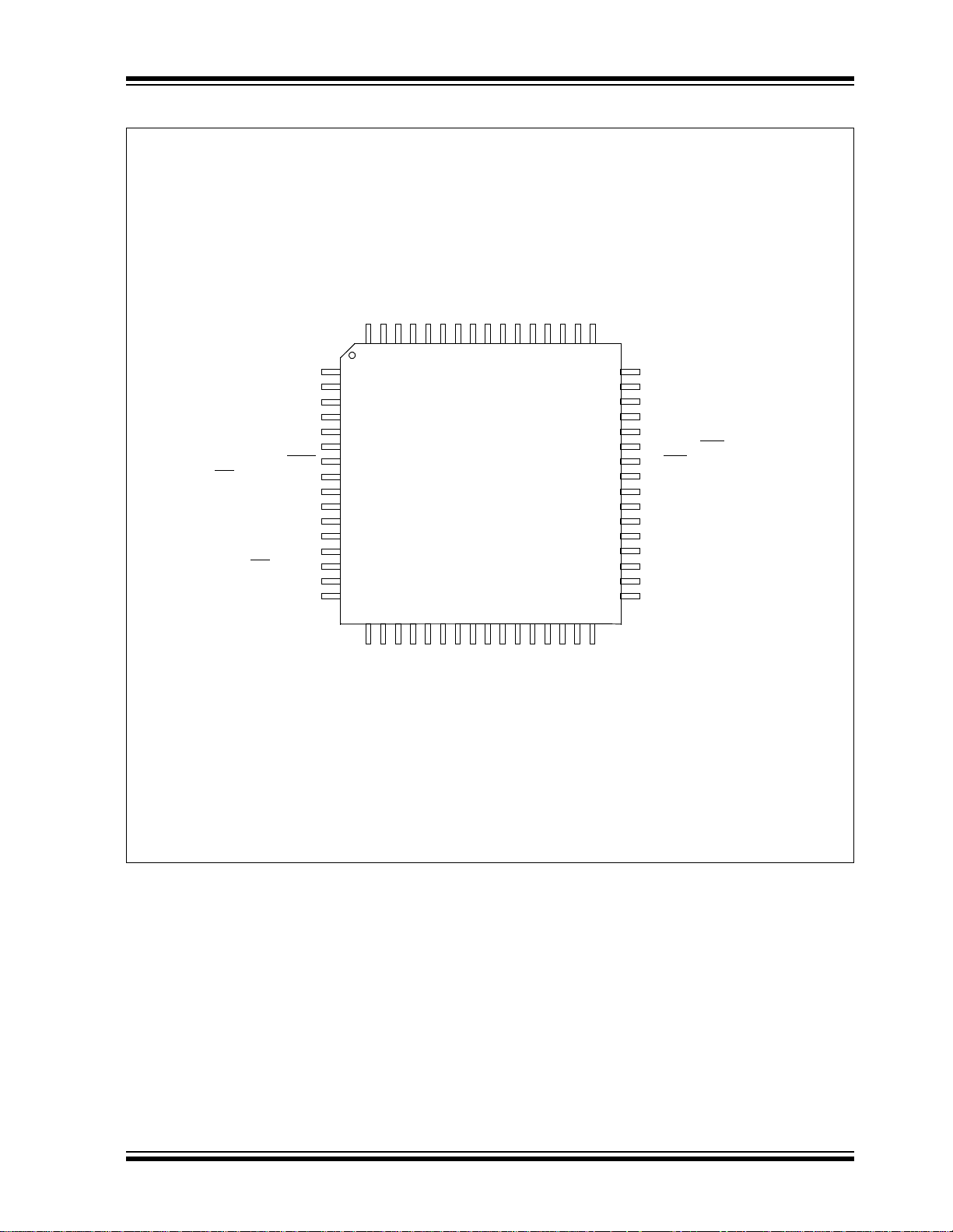
Page 6

dsPIC33F
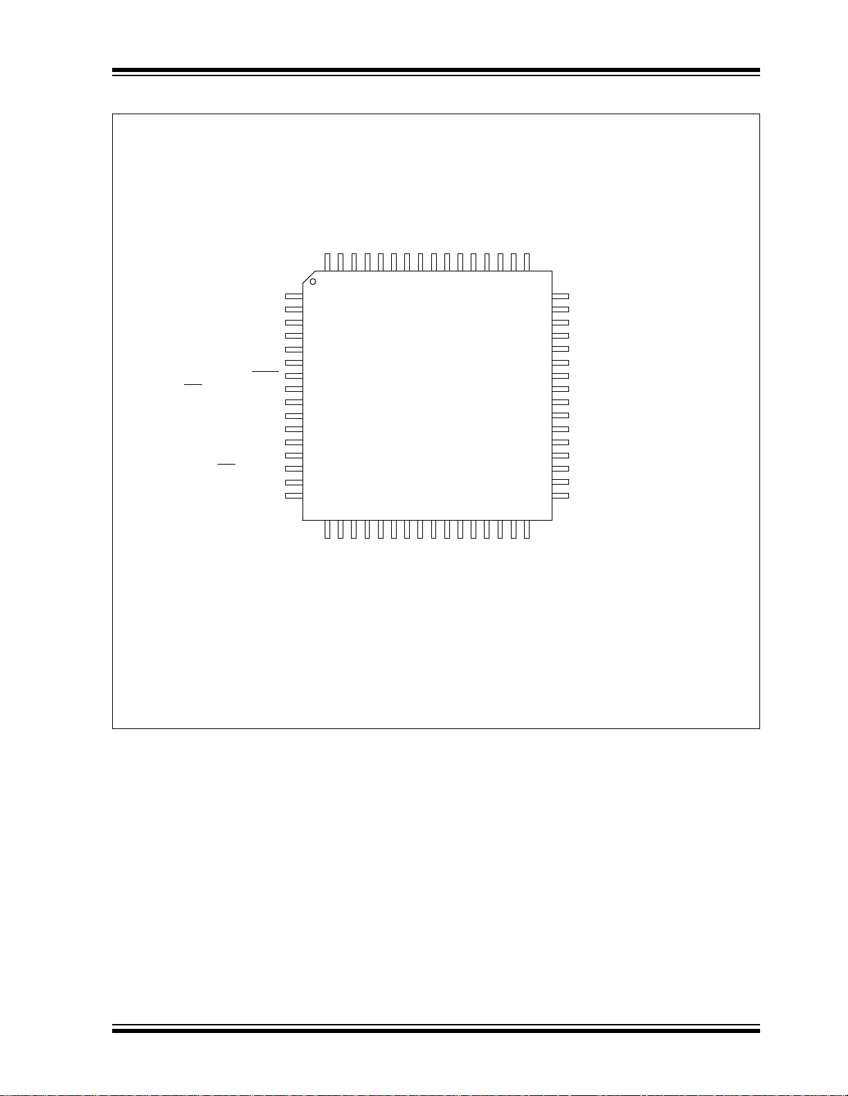
Pin Diagrams
64-Pin TQFP
DDCORE
CSDO/RG13
CSDI/RG12
CSCK/RG14
RG1
RF1
RG0
OC8/CN16/RD7
V
VDD
RF0
OC7/CN15/RD6
OC6/IC6/CN14/RD5
OC5/IC5/CN13/RD4
OC4/RD3
OC3/RD2
OC2/RD1
AN16/T2CK/T7CK/RC1
AN17/T3CK/T6CK/RC2
SDO2/CN10/RG8
/T5CK/CN11/RG9
SS2
AN5/IC8/CN7/RB5
AN4/IC7/CN6/RB4
PGC3/EMUC3/AN1/V
PGD3/EMUD3/AN0/V
AN2/SS1
COFS/RG15
SCK2/CN8/RG6
SDI2/CN9/RG7
MCLR
VSS
VDD
AN3/CN5/RB3
/CN4/RB2
REF-/CN3/RB1
REF+/CN2/RB0
646362616059585756
1
2
3
4
5
6
7
8
9
10
11
12
13
14
15
16
dsPIC33FJ64GP206
dsPIC33FJ128GP206
171819202122232425
DD
AVSS
AV
U2CTS/AN8/RB8
PGD1/EMUD1/AN7/RB7
PGC1/EMUC1/AN6/OCFA/RB6
545352
55
27
26
SS
V
VDD
AN9/RB9
TDO/AN11/RB11
TMS/AN10/RB10
TCK/AN12/RB12
504951
48
PGC2/EMUC2/SOSCO/T1CK/CN0/RC14
47
PGD2/EMUD2/SOSCI/T4CK/CN1/RC13
46
OC1/RD0
IC4/INT4/RD11
45
44
IC3/INT3/RD10
IC2/U1CTS/INT2/RD9
43
IC1/INT1/RD8
42
V
41
SS
40
OSC2/CLKO/RC15
39
OSC1/CLKIN/RC12
38
V
DD
37
SCL1/RG2
36
SDA1/RG3
35
U1RTS/SCK1/INT0/RF6
34
U1RX/SDI1/RF2
33
U1TX/SDO1/RF3
32
31
30
29
28
TDI/AN13/RB13
U2TX/CN18/RF5
U2RX/CN17/RF4
U2RTS/AN14/RB14
AN15/OCFB/CN12/RB15
DS70165E-page 4 Preliminary © 2007 Microchip Technology Inc.
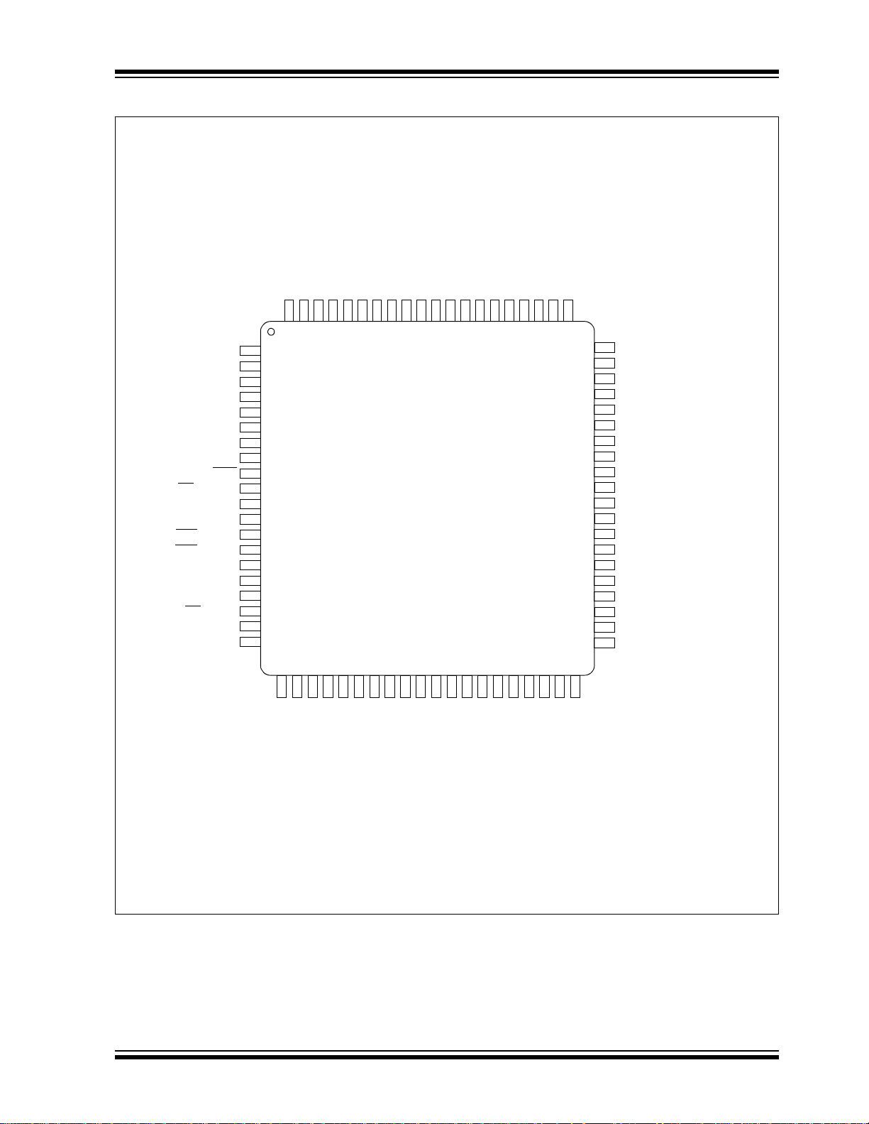
Page 7
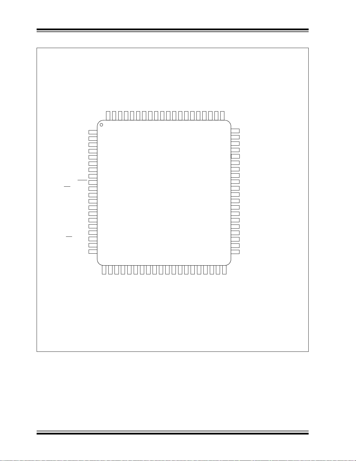
Pin Diagrams (Continued)
64-Pin TQFP
dsPIC33F
DDCORE
CSDO/RG13
CSDI/RG12
CSCK/RG14
RG1
RF1
RG0
OC8/CN16/RD7
V
VDD
RF0
OC7/CN15/RD6
OC6/IC6/CN14/RD5
OC5/IC5/CN13/RD4
OC4/RD3
OC3/RD2
OC2/RD1
AN16/T2CK/T7CK/RC1
AN17/T3CK/T6CK/RC2
SDO2/CN10/RG8
/T5CK/CN11/RG9
SS2
AN5/IC8/CN7/RB5
AN4/IC7/CN6/RB4
PGC3/EMUC3/AN1/V
PGD3/EMUD3/AN0/V
AN2/SS1
COFS/RG15
SCK2/CN8/RG6
SDI2/CN9/RG7
MCLR
VSS
VDD
AN3/CN5/RB3
/CN4/RB2
REF-/CN3/RB1
REF+/CN2/RB0
646362616059585756
1
2
3
4
5
6
7
8
9
10
11
12
13
14
15
16
dsPIC33FJ64GP306
dsPIC33FJ128GP306
171819202122232425
DD
AVSS
AV
U2CTS/AN8/RB8
PGD1/EMUD1/AN7/RB7
PGC1/EMUC1/AN6/OCFA/RB6
545352
55
27
26
SS
V
VDD
AN9/RB9
TDO/AN11/RB11
TMS/AN10/RB10
TCK/AN12/RB12
504951
48
PGC2/EMUC2/SOSCO/T1CK/CN0/RC14
47
PGD2/EMUD2/SOSCI/T4CK/CN1/RC13
46
OC1/RD0
IC4/INT4/RD11
45
44
IC3/INT3/RD10
IC2/U1CTS/INT2/RD9
43
IC1/INT1/RD8
42
V
41
SS
40
OSC2/CLKO/RC15
39
OSC1/CLKIN/RC12
38
V
DD
37
SCL1/RG2
36
SDA1/RG3
35
U1RTS/SCK1/INT0/RF6
34
U1RX/SDI1/RF2
33
U1TX/SDO1/RF3
32
31
30
29
28
TDI/AN13/RB13
U2RTS/AN14/RB14
U2TX/SCL2/CN18/RF5
U2RX/SDA2/CN17/RF4
AN15/OCFB/CN12/RB15
© 2007 Microchip Technology Inc. Preliminary DS70165E-page 5
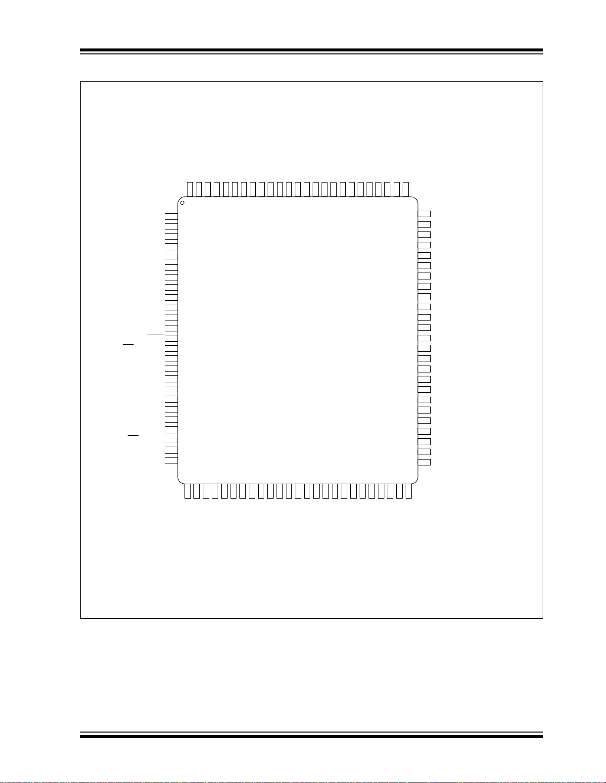
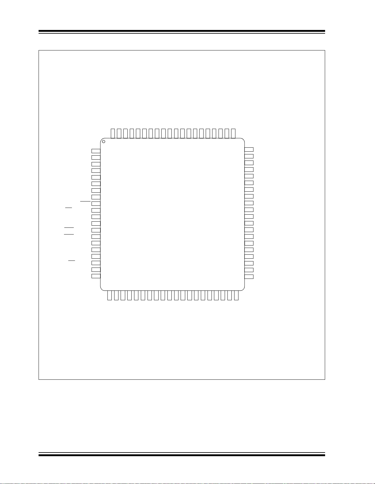
Page 8

dsPIC33F
Pin Diagrams (Continued)
64-Pin TQFP
CSDO/RG13
DDCORE
CSDI/RG12
CSCK/RG14
RG1
C1TX/RF1
RG0
OC8/CN16/RD7
V
VDD
C1RX/RF0
OC7/CN15/RD6
OC6/IC6/CN14/RD5
OC5/IC5/CN13/RD4
OC4/RD3
OC3/RD2
OC2/RD1
AN16/T2CK/T7CK/RC1
AN17/T3CK/T6CK/RC2
SDO2/CN10/RG8
/T5CK/CN11/RG9
SS2
AN5/IC8/CN7/RB5
AN4/IC7/CN6/RB4
PGC3/EMUC3/AN1/V
PGD3/EMUD3/AN0/V
AN2/SS1
COFS/RG15
SCK2/CN8/RG6
SDI2/CN9/RG7
MCLR
VSS
VDD
AN3/CN5/RB3
/CN4/RB2
REF-/CN3/RB1
REF+/CN2/RB0
646362616059585756
1
2
3
4
5
6
7
8
9
10
11
12
13
14
15
16
dsPIC33FJ256GP506
171819202122232425
DD
AVSS
AV
U2CTS/AN8/RB8
PGD1/EMUD1/AN7/RB7
PGC1/EMUC1/AN6/OCFA/RB6
AN9/RB9
545352
55
27
26
SS
V
VDD
TDO/AN11/RB11
TMS/AN10/RB10
TCK/AN12/RB12
504951
48
PGC2/EMUC2/SOSCO/T1CK/CN0/RC14
47
PGD2/EMUD2/SOSCI/T4CK/CN1/RC13
46
OC1/RD0
IC4/INT4/RD11
45
44
IC3/INT3/RD10
IC2/U1CTS/INT2/RD9
43
IC1/INT1/RD8
42
V
41
SS
40
OSC2/CLKO/RC15
39
OSC1/CLKIN/RC12
38
V
DD
37
SCL1/RG2
36
SDA1/RG3
35
U1RTS/SCK1/INT0/RF6
34
U1RX/SDI1/RF2
33
U1TX/SDO1/RF3
32
31
30
29
28
TDI/AN13/RB13
U2RTS/AN14/RB14
U2TX/SCL2/CN18/RF5
U2RX/SDA2/CN17/RF4
AN15/OCFB/CN12/RB15
DS70165E-page 6 Preliminary © 2007 Microchip Technology Inc.
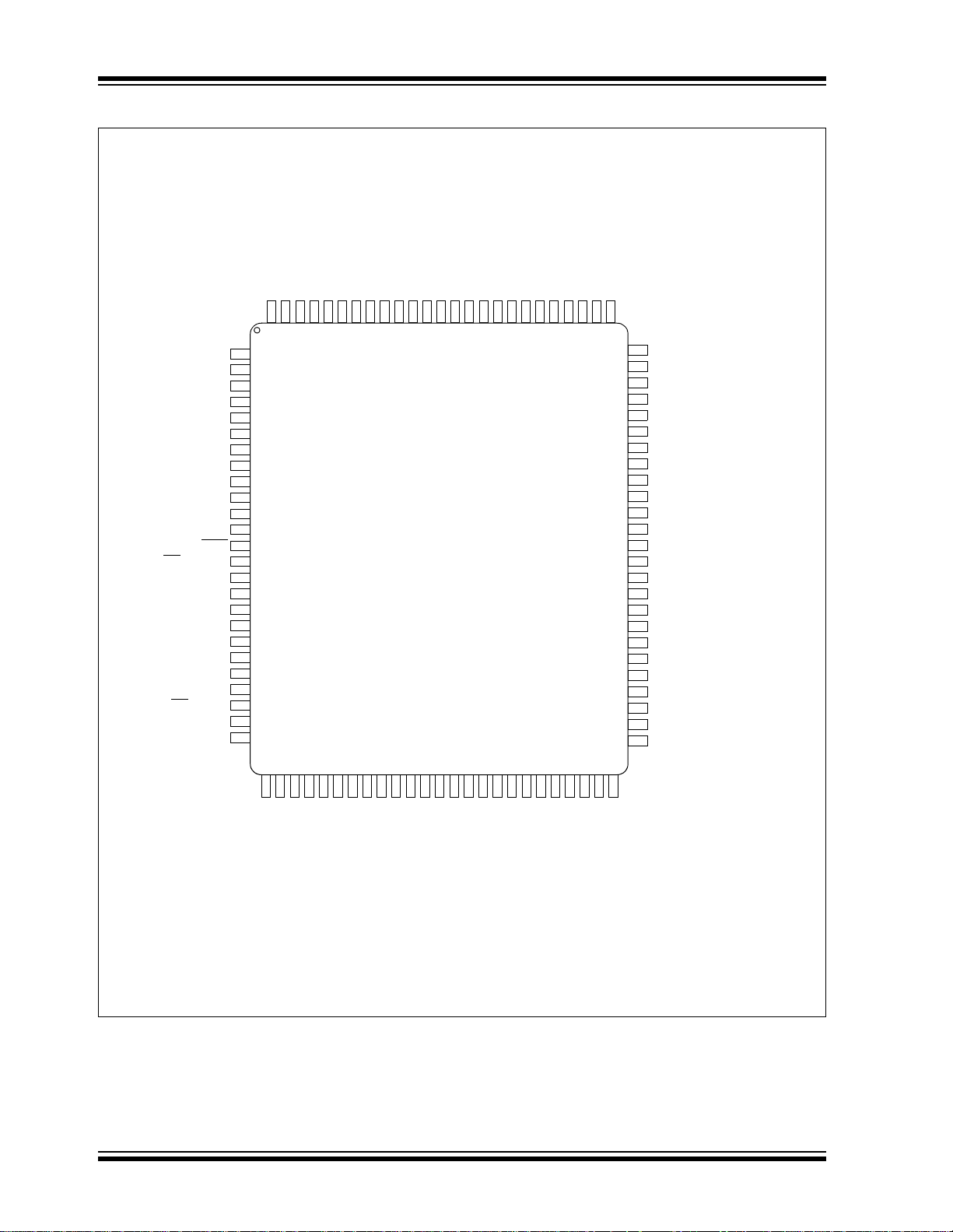
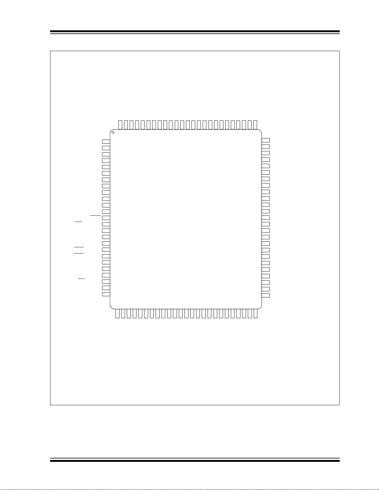
Page 9

Pin Diagrams (Continued)
64-Pin TQFP
dsPIC33F
DDCORE
CSDO/RG13
CSDI/RG12
CSCK/RG14
C2TX/RG1
C1TX/RF1
C2RX/RG0
OC8/CN16/RD7
V
VDD
C1RX/RF0
OC7/CN15/RD6
OC6/IC6/CN14/RD5
OC2/RD1
OC3/RD2
OC4/RD3
OC5/IC5/CN13/RD4
AN16/T2CK/T7CK/RC1
AN17/T3CK/T6CK/RC2
SDO2/CN10/RG8
/T5CK/CN11/RG9
SS2
AN5/IC8/CN7/RB5
AN4/IC7/CN6/RB4
PGC3/EMUC3/AN1/V
PGD3/EMUD3/AN0/V
AN2/SS1
COFS/RG15
SCK2/CN8/RG6
SDI2/CN9/RG7
MCLR
VSS
VDD
AN3/CN5/RB3
/CN4/RB2
REF-/CN3/RB1
REF+/CN2/RB0
646362616059585756
1
2
3
4
5
6
7
8
9
10
11
12
13
14
15
16
dsPIC33FJ64GP706
dsPIC33FJ128GP706
171819202122232425
DD
AVSS
AV
U2CTS/AN8/RB8
PGD1/EMUD1/AN7/RB7
PGC1/EMUC1/AN6/OCFA/RB6
AN9/RB9
545352
55
27
26
SS
V
VDD
TDO/AN11/RB11
TMS/AN10/RB10
TCK/AN12/RB12
504951
48
PGC2/EMUC2/SOSCO/T1CK/CN0/RC14
47
PGD2/EMUD2/SOSCI/T4CK/CN1/RC13
46
OC1/RD0
IC4/INT4/RD11
45
44
IC3/INT3/RD10
IC2/U1CTS/INT2/RD9
43
IC1/INT1/RD8
42
V
41
SS
40
OSC2/CLKO/RC15
39
OSC1/CLKIN/RC12
38
V
DD
37
SCL1/RG2
36
SDA1/RG3
35
U1RTS/SCK1/INT0/RF6
34
U1RX/SDI1/RF2
33
U1TX/SDO1/RF3
32
31
30
29
28
TDI/AN13/RB13
U2RTS/AN14/RB14
U2TX/SCL2/CN18/RF5
U2RX/SDA2/CN17/RF4
AN15/OCFB/CN12/RB15
© 2007 Microchip Technology Inc. Preliminary DS70165E-page 7
Page 10
dsPIC33F
Pin Diagrams (Continued)
80-Pin TQFP
COFS/RG15
AN16/T2CK/T7CK/RC1
AN17/T3CK/T6CK/RC2
AN18/T4CK/T9CK/RC3
AN19/T5CK/T8CK/RC4
SCK2/CN8/RG6
SDI2/CN9/RG7
SDO2/CN10/RG8
MCLR
SS2/CN11/RG9
V
V
TMS/AN20/INT1/RA12
TDO/AN21/INT2/RA13
AN5/CN 7/RB 5
AN4/CN 6/RB 4
AN3/CN 5/RB 3
AN2/SS1
/CN4/RB2
PGC3/EMUC3/AN1/CN3/RB1
PGD3/EMUD3/AN0/CN2/RB0
DD
CSCK/RG14
AN23/CN23/RA7
AN22/CN22/RA6
C2RX/RG0
CSDO/RG13
CSDI/RG12
792280
1
2
3
4
5
6
7
8
9
10
11
SS
12
13
14
15
16
17
18
19
20
21
2324252627282930313233
C2TX/RG1
75
767877
dsPIC33FJ64GP708
dsPIC33FJ128GP708
DDVDDCORE
C1TX/RF1
C1RX/RF0
727473
OC8/CN16/RD7
OC6/CN14/RD5
V
7170696867666564636261
OC7/CN15/RD6
34
OC5/CN13/RD4
35
IC5/RD12
OC4/RD3
OC3/RD2
IC6/CN19/RD13
36
OC2/RD1
PGC2/EMUC2/SOSCO/T1CK/CN0/RC14
60
PGD2 /E M U D 2 / S O S C I /CN1/RC13
59
OC1/RD0
58
IC4/RD11
57
IC3/RD10
56
IC2/RD9
55
IC1/RD8
54
SDA2/INT4/RA3
53
SCL2/INT3/RA2
52
SS
V
51
50
OSC2/CLKO/RC15
OSC 1/ C L KIN/RC12
49
DD
V
48
SCL1/RG2
47
SDA1/RG3
46
SCK1 /INT0/RF6
45
SDI1/RF7
44
43
SDO1/RF8
U1RX/RF2
42
U1TX/RF3
41
40
39
38
37
SS
DD
AV
AV
-/RA9
+/RA10
REF
V
REF
V
PGD1/EMUD1/AN7/RB7
PGC1/EMUC1/AN6/OCFA/RB6
AN9/RB9
U2CTS/AN8/RB8
SS
DD
V
V
AN11/RB1 1
AN10/RB10
TDI/AN13/RB13
TCK/AN12/RB12
U2RTS/AN14/RB14
IC7/U1CTS/CN20/RD14
AN15/OC FB/ C N1 2/ RB 15
U2TX/CN18/RF5
U2RX/CN17/RF4
IC8/U1RTS/CN21/RD15
DS70165E-page 8 Preliminary © 2007 Microchip Technology Inc.
Page 11
Pin Diagrams (Continued)
100-Pin TQFP
AN28/RE4
AN27/RE3
99
100
COFS/RG15
AN29/RE5
AN30/RE6
AN16/T2CK/T7CK/RC1
AN17/T3CK/T6CK/RC2
AN18/T4CK/T9CK/RC3
AN19/T5CK/T8CK/RC4
PGC3/EMUC3/AN1/CN3/RB1
PGD3/EMUD3/AN0/CN2/RB0
AN31/RE7
SCK2/CN8/RG6
SDI2/CN9/RG7
SDO2/CN10/RG8
MCLR
SS2/CN11/RG9
TMS/RA0
AN20 /INT1/RA12
AN21 /INT2/RA13
AN5/CN7/RB5
AN4/CN6/RB4
AN3/CN5/RB3
AN2/SS1
/CN4/RB2
1
V
2
DD
3
4
5
6
7
8
9
10
11
12
13
14
V
SS
15
DD
V
16
17
18
19
20
21
22
23
24
25
AN26/RE2
AN23/CN23/RA7
CSDO/RG13
CSDI/RG12
CSCK/RG14
95
969897
AN22/CN22/RA6
AN25/RE1
AN24/RE0
9294939190898887868584838281807978
dsPIC33FJ64GP310
dsPIC33FJ128GP310
dsPIC33F
DDCORE
RG0
DD
RF0
V
RG1
RF1
OC6/CN14/RD5
OC5/CN13/RD4
IC6/CN19/RD13
IC5/RD12
OC4/RD3
OC3/RD2
V
OC8/CN16/RD7
OC7/CN15/RD6
OC2/RD1
76
77
V
SS
75
PGC2/EMUC2/SOSCO/T1CK/CN0/RC14
74
PGD2/EMUD2/SOSCI/CN1/RC13
73
OC1/RD0
72
IC4/RD11
71
IC3/RD10
70
IC2/RD9
69
IC1/RD8
68
INT4/R A15
67
INT3/R A14
66
V
SS
65
OSC2/CLKO/RC15
64
OSC1/CLKIN/RC12
63
DD
V
62
TDO/RA5
61
TDI/RA4
60
SDA2/RA3
59
SCL2/RA2
58
SCL1/RG2
57
SDA1/RG3
56
SCK1 /INT0/RF6
55
SDI1/R F7
54
SDO1/RF8
53
U1RX/RF2
52
U1TX/RF3
51
26
2829303132333435363738
27
SS
DD
AV
AV
-/RA9
+/RA10
PGD1/EMUD1/AN7/RB7
PGC1/EMUC1/AN6/OCFA/RB6
REF
V
AN8/RB8
REF
V
AN9/RB9
AN10/RB10
41
40
39
SS
DD
V
V
TCK/RA1
AN11/RB1 1
AN12/RB12
U2RTS/RF13
U2CTS/RF12
42
AN13/RB13
43
AN14/RB14
44
AN15/OCFB/CN12/RB15
45
4647484950
SS
DD
V
V
IC8/U1RTS/CN21/RD15
IC7/U1CTS/CN20/RD14
U2RX/CN17/RF4
U2TX/CN18/RF5
© 2007 Microchip Technology Inc. Preliminary DS70165E-page 9
Page 12
dsPIC33F
Pin Diagrams (Continued)
100-Pin TQFP
AN28/RE4
AN27/RE3
99
100
COFS/RG15
AN29/RE5
AN30/RE6
AN31/RE7
AN16/T2CK/T7CK/RC1
AN17/T3CK/T6CK/RC2
AN18/T4CK/T9CK/RC3
AN19/T5CK/T8CK/RC4
SCK2/CN8/RG6
SDI2/CN9/RG7
SDO2/CN10/RG8
MCLR
SS2/CN11/RG9
TMS/RA0
AN20 /INT1/RA12
AN21 /INT2/RA13
AN5/CN7/RB5
AN4/CN6/RB4
AN3/CN5/RB3
AN2/SS1
/CN4/RB2
PGC3/EMUC3/AN1/CN3/RB1
PGD3/EMUD3/AN0/CN2/RB0
1
2
DD
V
3
4
5
6
7
8
9
10
11
12
13
14
SS
V
15
16
DD
V
17
18
19
20
21
22
23
24
25
AN26/RE2
AN23/CN23/RA7
CSDO/RG13
CSDI/RG12
CSCK/RG14
95
969897
AN22/CN22/RA6
AN25/RE1
AN24/RE0
9294939190898887868584838281807978
dsPIC33FJ256GP510
RG0
RG1
C1TX/RF1
DD
C1RX/RF0
V
DDCORE
OC6/CN14/RD5
OC5/CN13/RD4
IC6/CN19/RD13
IC5/RD12
OC4/RD3
OC3/RD2
V
OC8/CN16/RD7
OC7/CN15/RD6
OC2/RD1
76
77
75
V
SS
74
PGC2/EMUC2/SOSCO/T1CK/CN0/RC14
73
PGD2/EMUD2/SOSCI/CN1/RC13
OC1/RD0
72
IC4/RD11
71
IC3/RD10
70
IC2/RD9
69
IC1/RD8
68
INT4/R A15
67
66
INT3/R A14
V
SS
65
OSC2/CLKO/RC15
64
OSC1/CLKIN/RC12
63
V
DD
62
TDO/RA5
61
TDI/RA4
60
SDA2/RA3
59
SCL2/RA2
58
SCL1/RG2
57
SDA1/RG3
56
SCK1 /INT0/RF6
55
SDI1/R F7
54
SDO1/RF8
53
U1RX/RF2
52
51
U1TX/RF3
26
2829303132333435363738
27
SS
DD
AV
AV
-/RA9
+/RA10
REF
V
PGD1/EMUD1/AN7/RB7
PGC1/EMUC1/AN6 /OCFA/RB 6
AN8/RB8
REF
V
AN9/RB9
AN10/RB10
41
40
39
SS
DD
V
V
TCK/RA1
AN11/RB1 1
AN12/RB12
U2CTS/RF12
U2RTS/RF13
45
44
43
42
AN13/RB13
AN14/RB14
SS
V
AN15/OCFB/CN12/RB15
4647484950
DD
V
U2RX/CN17/RF4
IC8/U1RTS/CN21/RD15
IC7/U1CTS/CN20/RD14
U2TX/CN18/RF5
DS70165E-page 10 Preliminary © 2007 Microchip Technology Inc.
Page 13

Pin Diagrams (Continued)
100-Pin TQFP
AN28/RE4
AN27/RE3
99
100
COFS/RG15
AN29/RE5
AN30/RE6
AN16/T2CK/T7CK/RC1
AN17/T3CK/T6CK/RC2
AN18/T4CK/T9CK/RC3
AN19/T5CK/T8CK/RC4
PGC 3 /E M U C 3 /A N 1 /C N3/RB1
PGD 3 /E M U D 3 /A N 0 /C N2/RB0
AN31/RE7
SCK2/CN8/RG6
SDI2/CN9/RG7
SDO2/CN10/RG8
MCLR
SS2/CN11/RG9
TMS/RA0
AN20/INT1/RA12
AN21/INT2/RA13
AN5/CN7/RB5
AN4/CN6/RB4
AN3/CN5/RB3
AN2/SS1
/CN4/RB2
1
DD
V
2
3
4
5
6
7
8
9
10
11
12
13
14
V
SS
15
V
DD
16
17
18
19
20
21
22
23
24
25
AN26/RE2
AN23/CN23/RA7
CSDO/RG13
CSDI/RG12
CSCK/RG14
95
969897
AN22/CN22/RA6
AN25/RE1
AN24/RE0
9294939190898887868584838281807978
dsPIC33FJ64GP710
dsPIC33FJ128GP710
dsPIC33FJ256GP710
C2RX/RG0
dsPIC33F
DDCORE
DD
C1RX/RF0
V
C2TX/RG1
C1TX/RF1
OC6/CN1 4/R D5
OC5/CN1 3/R D4
IC6/CN19/RD 13
IC5/RD12
OC4/RD3
OC3/RD2
V
OC8/CN1 6/R D7
OC7/CN1 5/R D6
OC2/RD1
76
77
V
SS
75
74
PGC2/EMUC2/SOSCO/T1CK/CN0/RC14
PGD2/EMUD2/SOSCI/CN1/RC13
73
OC1/RD0
72
71
IC4/RD11
IC3/RD10
70
IC2/RD9
69
68
IC1/RD8
INT4/RA15
67
66
INT3/RA14
V
SS
65
OSC2/CLKO/RC15
64
OSC1/CLKIN/RC1 2
63
DD
V
62
TDO/RA5
61
TDI/RA4
60
SDA2/RA3
59
SCL2/RA2
58
SCL1/RG2
57
SDA1/RG3
56
SCK1/INT0/RF6
55
SDI1/RF7
54
SDO1/RF8
53
U1RX/RF2
52
51
U1TX/RF3
26
2829303132333435363738
27
SS
DD
AV
AV
-/RA9
+/RA10
REF
V
PGD1/EMUD1/AN7/RB7
PGC1/EMUC1/AN6/OCFA/RB6
AN8/RB8
REF
V
AN9/RB9
41
40
39
SS
DD
V
V
TCK/RA1
AN11/RB1 1
AN10/RB1 0
AN12/RB1 2
U2RTS/RF13
U2CTS/RF12
45
44
43
42
AN13/RB1 3
AN14/RB1 4
SS
V
AN15/OCFB/CN12/RB15
4647484950
DD
V
U2RX/CN17/RF4
IC8/U1RTS/CN21/RD15
IC7/U1CTS/CN20/RD14
U2TX/CN18/RF5
© 2007 Microchip Technology Inc. Preliminary DS70165E-page 11
Page 14

dsPIC33F
dsPIC33F Motor Control Family Variants
Progra
Device Pins
dsPIC33FJ64MC506 64 64 8 9 8 8 8 ch 1 0 1 ADC,
dsPIC33FJ64MC508 80 64 8 9 8 8 8 ch 1 0 1 ADC,
dsPIC33FJ64MC510 100 64 8 9 8 8 8 ch 1 0 1 ADC,
dsPIC33FJ64MC706 64 64 16 9 8 8 8 ch 1 0 2 ADC,
dsPIC33FJ64MC710 100 64 16 9 8 8 8 ch 1 0 2 ADC,
dsPIC33FJ128MC506 64 128 8 9 8 8 8 ch 1 0 1 ADC,
dsPIC33FJ128MC510 100 128 8 9 8 8 8 ch 1 0 1 ADC,
dsPIC33FJ128MC706 64 128 16 9 8 8 8 ch 1 0 2 ADC,
dsPIC33FJ128MC708 80 128 16 9 8 8 8 ch 1 0 2 ADC,
dsPIC33FJ128MC710 100 128 16 9 8 8 8 ch 1 0 2 ADC,
dsPIC33FJ256MC510 100 256 16 9 8 8 8 ch 1 0 1 ADC,
dsPIC33FJ256MC710 100 256 30 9 8 8 8 ch 1 0 2 ADC,
Note 1: RAM size is inclusive of 2 Kbytes DMA RAM.
2: Maximum I/O pin count includes pins shared by the peripheral functions.
m Flash
Memory
(Kbyte)
RAM
(Kbyte)
(1)
Timer 16-bit
Std. PWM
Input Capture
Output Comp are
Interface
Motor Control PWM
Quadrature Encoder
ADC
Codec Interface
16 ch
18 ch
24 ch
16 ch
24 ch
16 ch
24 ch
16 ch
18 ch
24 ch
24 ch
24 ch
(2)
Enhanced CAN
Packages
I/O Pins (Max)
C™
SPI
2
UART
222153 PT
222169 PT
222185PF, PT
222153 PT
222285PF, PT
222153 PT
222185PF, PT
222153 PT
222269 PT
222285PF, PT
222185PF, PT
222285PF, PT
I
DS70165E-page 12 Preliminary © 2007 Microchip Technology Inc.
Page 15
Pin Diagrams
64-Pin TQFP
PWM3L/RE4
PWM2H/RE3
PWM2L/RE2
PWM1L/RE0
PWM1H/RE1
dsPIC33F
DDCORE
OC8/UPDN/CN16/RD7
V
C1TX/RF1
VDDC1RX/RF0
OC7/CN15/RD6
OC6/IC6/CN14/RD5
OC2/RD1
OC3/RD2
OC4/RD3
OC5/IC5/CN13/RD4
SDO2/CN10/RG8
SS2/T5CK/CN11/RG9
AN5/QEB/IC8/CN7/RB5
AN4/QEA/IC7/CN6/RB4
AN3/INDX/CN5/RB3
AN2/SS1
PGC3/EMUC3/AN1/V
PGD3/EMUD3/AN0/V
PWM3H/RE5
PWM4L/RE6
PWM4H/RE7
SCK2/CN8/RG6
SDI2/CN9/RG7
MCLR
V
V
/CN4/RB2
REF
-/CN3/RB1
REF
+/CN2/RB0
SS
DD
646362616059585756
1
2
3
4
5
6
7
8
9
10
11
12
13
14
15
16
dsPIC33FJ64MC506
171819202122232425
SS
DD
AV
AV
U2CTS/AN8/RB8
PGD1/EMUD1/AN7/RB7
PGC1/EMUC1/AN6/OCFA/RB6
545352
55
27
26
SS
DD
V
V
AN9/RB9
TDO/AN11/RB11
TMS/AN10/RB10
TCK/AN12/RB12
504951
48
PGC2/EMUC2/SOSCO/T1CK/CN0/RC14
47
PGD2/EMUD2/SOSCI/T4CK/CN1/RC13
46
OC1/RD0
IC4/INT4/RD11
45
44
IC3/INT3/RD10
IC2/U1CTS/FLTB
43
IC1/FLTA
42
41
V
SS
40
OSC2/CLKO/RC15
39
OSC1/CLKIN/RC12
DD
V
38
SCL1/RG2
37
SDA1/RG3
36
U1RTS/SCK1/INT0/RF6
35
U1RX/SDI1/RF2
34
33
U1TX/SDO1/RF3
32
31
30
29
28
TDI/AN13/RB13
U2TX/CN18/RF5
U2RX/CN17/RF4
U2RTS/AN14/RB14
AN15/OCFB/CN12/RB15
/INT2/RD9
/INT1/RD8
© 2007 Microchip Technology Inc. Preliminary DS70165E-page 13
Page 16

dsPIC33F
Pin Diagrams (Continued)
64-Pin TQFP
PWM3L/RE4
PWM2H/RE3
PWM2L/RE2
PWM1H/RE1
PWM1L/RE0
C1TX/RF1
VDDC1RX/RF0
DDCORE
OC8/UPDN/CN16/RD7
V
OC7/CN15/RD6
OC6/IC6/CN14/RD5
OC2/RD1
OC3/RD2
OC4/RD3
OC5/IC5/CN13/RD4
SDO2/CN10/RG8
SS2/T5CK/CN11/RG9
AN5/QEB/IC8/CN7/RB5
AN4/QEA/IC7/CN6/RB4
AN3/INDX/CN5/RB3
AN2/SS1
PGC3/EMUC3/AN1/V
PGD3/EMUD3/AN0/V
PWM3H/RE5
PWM4L/RE6
PWM4H/RE7
SCK2/CN8/RG6
SDI2/CN9/RG7
MCLR
V
V
/CN4/RB2
REF
-/CN3/RB1
REF
+/CN2/RB0
SS
DD
646362616059585756
1
2
3
4
5
6
7
8
9
10
11
12
13
14
15
16
dsPIC33FJ128MC506
dsPIC33FJ64MC506
dsPIC33FJ128MC706
171819202122232425
SS
DD
AV
AV
U2CTS/AN8/RB8
PGD1/EMUD1/AN7/RB7
PGC1/EMUC1/AN6/OCFA/RB6
AN9/RB9
TDO/AN11/RB11
TMS/AN10/RB10
29
28
TDI/AN13/RB13
U2RTS/AN14/RB14
504951
48
47
46
45
44
43
42
41
40
39
38
37
36
35
34
33
32
31
30
U2TX/SCL2/CN18/RF5
U2RX/SDA2/CN17/RF4
AN15/OCFB/CN12/RB15
PGC2/EMUC2/SOSCO/T1CK/CN0/RC 14
PGD2/EMUD2/SOSCI/T4CK/CN1/RC13
OC1/RD0
IC4/INT4/RD11
IC3/INT3/RD10
IC2/U1CTS/
IC1/
V
OSC2/CLKO/RC15
OSC1/CLKIN/RC12
V
SCL1/RG2
SDA1/RG3
U1RTS/SCK1/INT0/RF6
U1RX/SDI1/RF2
U1TX/SDO1/RF3
SS
DD
FLTA
FLTB
/INT2/RD9
/INT1/RD8
545352
55
27
26
SS
DD
V
V
TCK/AN12/RB12
DS70165E-page 14 Preliminary © 2007 Microchip Technology Inc.
Page 17
Pin Diagrams (Continued)
80-Pin TQFP
PWM3L/RE4
PWM2L/RE2
PWM2H/RE3
PWM1H/RE1
PWM1L/RE0
dsPIC33F
DDVDDCORE
RG0
RG1
V
C1TX/RF1
C1RX/RF0
OC8/CN16/UPDN/RD7
OC6/CN14/RD5
OC7/CN15/RD6
OC5/CN13/RD4
IC5/RD12
OC4/RD3
OC3/RD2
IC6/CN19/RD13
OC2/RD1
PWM3H/RE5
PWM4L/RE6
PWM4H/RE7
AN16/T2CK/T7CK/RC1
AN17/T3CK/T6CK/RC2
SCK2/CN8/RG6
SDI2/CN9/RG7
SDO2/CN10/RG8
MCLR
SS2/CN11/RG9
V
V
FLTA
/INT1/RE8
TMS/
TDO/
FLTB
/INT2/RE9
AN5/QEB/CN7/RB5
AN4/QEA/CN6/RB4
AN3/IN DX/CN5/RB3
AN2/SS1
/CN4/RB2
PGC 3 /E M U C 3 /A N 1 /C N3/RB1
PGD 3 /E M U D 3 /A N 0 /C N2/RB0
SS
DD
U2CTS/AN8/RB8
727473
7170696867666564636261
35
34
SS
DD
V
V
AN9/RB9
AN11/RB1 1
AN10/RB10
TDI/AN13/RB13
TCK/AN12/RB12
U2RTS/AN14/RB14
60
PGC2/EMUC2/SOSCO/T1CK/CN0/RC14
PGD2/EMUD2/SOSCI/CN1/RC13
59
OC1/RD0
58
IC4/RD11
57
56
IC3/RD10
IC2/RD9
55
IC1/RD8
54
SDA2/INT4/RA3
53
52
SCL2 /INT3/RA2
SS
V
51
OSC2/CLKO/RC15
50
OSC1/CLKIN/RC12
49
V
48
47
46
45
44
43
42
41
40
39
38
37
36
U2TX/CN18/RF5
U2RX/CN17/RF4
IC8/U1RTS/CN21/RD15
IC7/U1CTS/CN20/RD14
AN15/OCFB/CN12/RB15
DD
SCL1/RG2
SDA1/RG3
SCK1/INT0/RF6
SDI1/RF7
SDO1/RF8
U1RX/RF2
U1TX/RF3
75
792280
1
2
3
4
5
6
7
8
9
10
11
12
13
14
15
16
17
18
19
20
21
PGD1/EMUD1/AN7/RB7
PGC1/EMUC1/AN6 /OCFA/RB 6
767877
dsPIC33FJ64MC508
2324252627282930313233
SS
DD
AV
AV
-/RA9
+/RA10
REF
V
REF
V
© 2007 Microchip Technology Inc. Preliminary DS70165E-page 15
Page 18
dsPIC33F
Pin Diagrams (Continued)
80-Pin TQFP
PWM3H/RE5
PWM4L/RE6
PWM4H/RE7
AN16/T2CK/T7CK/RC1
AN17/T3CK/T6CK/RC2
SCK2/CN8/RG6
SDI2/C N9/RG7
SDO2/CN10/RG8
MCLR
SS2/CN11/RG9
V
V
FLTA
/INT1/R E8
TMS/
FLTB
TDO/
PGC3/EMUC3/AN1/CN3/RB1
PGD3/EMUD3/AN0/CN2/RB0
/INT2/R E9
AN5/QEB/CN7/RB5
AN4/QEA/CN6/RB4
AN3/INDX/CN5/RB3
AN2/SS1
/CN4/RB2
SS
DD
PWM2L/RE2
PWM1H/RE1
PWM1L/RE0
CRX2/RG0
PWM3L/RE4
PWM2H/RE3
792280
1
2
3
4
5
6
7
8
9
10
11
12
13
14
15
16
17
18
19
20
21
2324252627282930313233
C2TX/RG1
75
767877
dsPIC33FJ128MC708
DDVDDCORE
C1TX/RF1
C1RX/RF0
727473
OC8/CN16/UPDN/RD7
OC6/CN14/RD5
V
7170696867666564636261
OC7/CN15/RD6
IC5/RD12
OC4/RD3
OC3/RD2
OC5/CN13/RD4
IC6/CN19/R D1 3
36
35
34
OC2/RD1
60
PGC2/EMUC2/SOSCO/T1CK/CN0/RC14
PGD2/EMUD2/SOSCI/CN1/RC13
59
OC1/RD0
58
IC4/RD11
57
IC3/RD10
56
IC2/RD9
55
IC1/RD8
54
SDA2/INT4/RA3
53
SCL2 /INT3/RA2
52
SS
V
51
OSC2/CLKO/RC15
50
OSC1/CLKIN/RC12
49
48
DD
V
SCL1/RG2
47
SDA1/RG3
46
SCK1/INT0/RF6
45
SDI1/RF7
44
SDO1/RF8
43
U1RX/RF2
42
U1TX/RF3
41
40
39
38
37
SS
DD
AV
AV
-/RA9
+/RA10
REF
V
REF
V
PGD1/EMUD1/AN7 /RB7
PGC1/EMUC1/AN6/OCFA/RB6
AN9/RB9
U2CTS/AN8/RB8
AN10/RB10
SS
DD
V
V
AN11/RB1 1
TDI/AN13/RB13
TCK/AN12/RB12
U2RTS/AN14/RB14
AN15/OCFB/CN12/RB15
IC7/U1CTS/CN20/RD14
U2TX/CN18/RF5
U2RX/CN17/RF4
IC8/U1RTS/CN21/RD15
DS70165E-page 16 Preliminary © 2007 Microchip Technology Inc.
Page 19
Pin Diagrams (Continued)
100-Pin TQFP
PWM3L/RE4
PWM2H/RE3
99
100
DD
DD
1
2
3
4
5
6
7
8
9
10
11
12
13
14
SS
15
16
17
18
19
20
21
22
23
24
25
COFS/RG15
V
PWM3H/RE5
PWM4L/RE6
PWM4H/RE7
AN16/T2CK/T7CK/RC1
AN17/T3CK/T6CK/RC2
AN18/T4CK/T9CK/RC3
AN19/T5CK/T8CK/RC4
SCK2/CN8/RG6
SDI2/C N9/RG7
SDO2/CN10/RG8
MCLR
SS2/CN11/RG9
FLTA
AN20/
AN21/
FLTB
AN5/QEB/CN7/RB5
AN4/QEA/CN6/RB4
AN3/INDX/CN5/RB3
AN2/SS1
PGC3/EMUC3/AN1/CN3/RB1
PGD3/EMUD3/AN0/CN2/RB0
V
V
TMS/RA0
/INT1/R E8
/INT2/R E9
/CN4/RB2
dsPIC33F
DDCORE
DD
RG1
PWM2L/RE2
CSDO/RG13
CSDI/RG12
969897
AN23/CN23/RA7
CSCK/RG14
PWM1H/RE1
PWM1L/RE0
9294939190898887868584838281807978
95
C1TX/RF1
AN22/CN22/RA6
RG0
dsPIC33FJ64MC510
OC8/UPDN//CN16/RD7
OC7/CN15/RD6
OC6/CN14/RD5
OC5/CN13/RD4
IC6/CN19/RD13
IC5/RD12
OC4/RD3
OC3/RD2
C1RX/RF0
V
V
OC2/RD1
76
77
V
75
SS
74
PGC2/EMUC2/SOSCO/T1CK/CN0/RC14
73
PGD2/EMUD2/SOSCI/CN1/RC13
72
OC1/RD0
IC4/RD11
71
IC3/RD10
70
IC2/RD9
69
68
IC1/RD8
INT4/RA15
67
66
INT3/RA14
V
SS
65
OSC2/CLKO/RC15
64
OSC1/CLKIN/RC1 2
63
DD
V
62
TDO/RA5
61
TDI/RA4
60
RA3
59
RA2
58
57
SCL1/RG2
SDA1/RG3
56
SCK1/INT0/RF6
55
SDI1/RF7
54
SDO1/RF8
53
U1RX/RF2
52
U1TX/RF3
51
26
2829303132333435363738
27
SS
DD
AV
AV
-/RA9
+/RA10
REF
V
PGD1/EMUD1/AN7/RB7
PGC1/EMUC1/AN6/OCFA/RB6
AN8/RB8
REF
V
AN9/RB9
AN10/RB10
41
40
39
SS
DD
V
V
TCK/RA1
AN11/RB1 1
AN12/RB12
U2RTS/RF13
U2CTS/RF12
42
AN13/RB13
43
AN14/RB14
44
AN15/OCFB/CN12/RB15
45
4647484950
SS
DD
V
V
IC8/U1RTS/CN21/RD15
IC7/U1CTS/CN20/RD14
U2RX/CN17/RF4
U2TX/CN18/RF5
© 2007 Microchip Technology Inc. Preliminary DS70165E-page 17
Page 20
dsPIC33F
Pin Diagrams (Continued)
100-Pin TQFP
PWM3L/RE4
PWM2H/RE3
99
100
COFS/RG15
PWM3H/RE5
PWM4L/RE6
PWM4H/RE7
AN16/T2CK/T7CK/RC1
AN17/T3CK/T6CK/RC2
AN18/T4CK/T9CK/RC3
AN19/T5CK/T8CK/RC4
SCK2/CN8/RG6
SDI2/C N9/RG7
SDO2/CN10/RG8
MCLR
SS2/CN11/RG9
TMS/RA0
AN20/
FLTA
/INT1/R E8
AN21/
FLTB
/INT2/R E9
AN5/QEB/CN7/RB5
AN4/QEA/CN6/RB4
AN3/INDX/CN5/RB3
AN2/SS1
/CN4/RB2
PGC3/EMUC3/AN1/CN3/RB1
PGD3/EMUD3/AN0/CN2/RB0
1
V
DD
2
3
4
5
6
7
8
9
10
11
12
13
14
SS
V
15
V
DD
16
17
18
19
20
21
22
23
24
25
PWM2L/RE2
RG1
DD
C1RX/RF0
V
C1TX/RF1
AN23/CN23/RA7
CSDO/RG13
CSDI/RG12
CSCK/RG14
95
969897
AN22/CN22/RA6
PWM1H/RE1
PWM1L/RE0
RG0
9294939190898887868584838281807978
dsPIC33FJ128MC510
dsPIC33FJ256MC510
OC6/CN14/RD5
OC5/CN13/RD4
IC6/CN19/RD13
IC5/RD12
OC4/RD3
OC3/RD2
V
OC8/UPDN//CN16/RD7
OC7/CN15/RD6
OC2/RD1
76
77
V
75
74
73
72
71
70
69
68
67
66
65
64
63
62
61
60
59
58
57
56
55
54
53
52
51
SS
PGC2/EMUC2/SOSCO/T1CK/CN0/RC14
PGD2/EMUD2/SOSCI/CN1/RC13
OC1/RD0
IC4/RD11
IC3/RD10
IC2/RD9
IC1/RD8
INT4/R A15
INT3/R A14
V
SS
OSC2/CLKO/RC15
OSC1/CLKIN/RC12
V
DD
TDO/RA5
TDI/RA4
SDA2/RA3
SCL2/RA2
SCL1/RG2
SDA1/RG3
SCK1 /INT0/RF6
SDI1/RF7
SDO1/RF8
U1RX/RF2
U1TX/RF3
DDCORE
26
2829303132333435363738
27
SS
DD
AV
AV
-/RA9
+/RA10
PGC1/EMUC1/AN6/OCFA/RB6
PGD1/EMUD1/AN7/RB7
REF
V
AN8/RB8
REF
V
AN9/RB9
41
40
39
SS
DD
V
V
TCK/RA1
AN11/RB1 1
AN10/RB10
AN12/RB12
U2RTS/RF13
U2CTS/RF12
45
44
43
42
AN13/RB13
AN14/RB14
AN15/OCFB/CN12/RB15
4647484950
SS
DD
V
V
IC8/U1RTS / CN 2 1/R D 15
IC7/U1CTS/CN20/RD14
U2TX/CN18/RF5
U2RX/CN17/RF4
DS70165E-page 18 Preliminary © 2007 Microchip Technology Inc.
Page 21
Pin Diagrams (Continued)
100-Pin TQFP
PWM3L/RE4
PWM2H/RE3
99
COFS/RG15
V
DD
PWM3H/RE5
PWM4L/RE6
PWM4H/RE7
AN16/T2CK/T7CK/RC1
AN17/T3CK/T6CK/RC2
AN18/T4CK/T9CK/RC3
AN19/T5CK/T8CK/RC4
SCK2/CN8/RG6
SDI2/CN9/RG7
SDO2/CN10/RG8
MCLR
SS2/CN11/RG9
AN20/
FLTA
AN21/
FLTB
AN5/QEB/CN7/RB5
AN4/QEA/CN6/RB4
AN3/INDX/CN5/RB3
AN2/SS1
PGC3/EMUC3/AN1/CN3/RB1
PGD3/EMUD3/AN0/CN2/RB0
V
V
TMS/RA0
/INT1/RE8
/INT2/RE9
/CN4/RB2
DD
SS
100
1
2
3
4
5
6
7
8
9
10
11
12
13
14
15
16
17
18
19
20
21
22
23
24
25
26
27
AN23/CN23/RA7
PWM2L/RE2
CSDO/RG13
CSDI/RG12
CSCK/RG14
95
969897
AN22/CN22/RA6
PWM1H/RE1
PWM1L/RE0
C2RX/RG0
C2TX/RG1
9294939190898887868584838281807978
dsPIC33FJ64MC710
dsPIC33FJ128MC710
dsPIC33FJ256MC710
2829303132333435363738
dsPIC33F
DDCORE
DD
C1RX/RF0
V
C1TX/RF1
40
39
OC6/CN1 4/R D5
OC5/CN1 3/R D4
IC6/CN19/RD 13
IC5/RD12
OC4/RD3
OC3/RD2
V
OC8/UPDN//CN16/RD7
OC7/CN1 5/R D6
45
44
43
42
41
4647484950
OC2/RD1
76
77
75
V
SS
74
PGC2/EMUC2/SOSCO/T1CK/CN0/RC14
73
PGD2/EMUD2/SOSCI/CN1/RC13
OC1/RD0
72
IC4/RD11
71
IC3/RD10
70
IC2/RD9
69
IC1/RD8
68
INT4/RA15
67
INT3/RA14
66
V
SS
65
OSC2/CLKO/RC15
64
OSC1/CLKIN/RC12
63
V
DD
62
TDO/RA5
61
TDI/RA4
60
SDA2/RA3
59
SCL2/RA2
58
57
SCL1/RG2
56
SDA1/RG3
SCK1/INT0/RF6
55
54
SDI1/RF7
53
SDO1/RF8
U1RX/RF2
52
51
U1TX/RF3
SS
DD
AV
AV
-/RA9
+/RA10
REF
V
PGD1/EMUD1/AN7/RB7
PGC1/EMUC1/AN6/OCFA/RB6
AN8/RB8
REF
V
AN9/RB9
SS
DD
V
V
TCK/RA1
AN11/RB1 1
AN10/RB10
AN12/RB12
U2RTS/RF13
U2CTS/RF12
SS
DD
V
V
AN13/RB13
AN14/RB14
U2TX/CN18/RF5
U2RX/CN17/RF4
IC8/U1RTS/CN21/RD15
IC7/U1CTS/CN20/RD14
AN15/OC F B/C N1 2/ RB 15
© 2007 Microchip Technology Inc. Preliminary DS70165E-page 19
Page 22

dsPIC33F
Table of Contents
dsPIC33F Product Families ................................................................................................................................................................... 3
1.0 Device Overview ........................................................................................................................................................................ 23
2.0 CPU............................................................................................................................................................................................ 27
3.0 Memory Organization.................................................................................................................................................................39
4.0 Flash Program Mem o ry................................... ........................................................................................................................... 77
5.0 Resets ....................................................................................................................................................................................... 83
6.0 Interrupt Controller ..................................................................................................................................................................... 87
7.0 Direct Memory Acc ess (DMA)................ ............................................................................ ...................................................... 135
8.0 Oscillator Configuration............................................................................................................................................................ 149
9.0 Power-Savi n g Features................................................................................................ ............................................................ 157
10.0 I/O Ports................................................................................................................................................................................... 159
11.0 Timer1...................................................................................................................................................................................... 161
12.0 Timer2/3, Timer4/5, Timer6/7 and Timer8/9 ............................................................................................................................163
13.0 Input Capture................................................................................................... .. .. .... .. ...............................................................169
14.0 Output Compare......................................... .......................... .................................................................................................... 171
15.0 Motor Control PWM Module. .................................................................................................................................................... 175
16.0 Quadrature Encoder Interface (QEI) Module ........................................................................................................................... 197
17.0 Serial Peripheral Interface (SPI)............................................................................................................................................... 205
18.0 Inter-Integrated Circuit (I
19.0 Universal Asynchronous Receiver Transmitter (UART) ...........................................................................................................223
20.0 Enhanced CAN Module................................................................ .. .. .. .. ....... .. .. .. .. .. .... ..... .. .. .. .................................................... 231
21.0 Data Converter Interface (DCI) Module....................................................................................................................................261
22.0 10-bit/12-bit Analog-to-Digital Converte r ( ADC)....................................................................... ................................................ 275
23.0 Special Features...................................................................................................................................................................... 289
24.0 Instruction Set Summary.......................................................................................................................................................... 297
25.0 Development Support............................................................................................................................................................... 305
26.0 Electrical Characteristics..........................................................................................................................................................309
27.0 Packaging Information. .............................................................................. ............................................................................... 351
Appendix A: Revision History............................................................................................................................................................. 357
Index ................................................................................................................................................................................................. 359
The Microchip Web Site....................................... .............................................................................................................................. 365
Customer Change Notification Service .............................................................................................................................................. 365
Customer Support.............................................................................................................................................................................. 365
Reader Response.............................................................................................................................................................................. 366
Product Identific ation System ............................................................................................................................................................ 367
2
C)..................................................................................................................................................... 213
DS70165E-page 20 Preliminary © 2007 Microchip Technology Inc.
Page 23

dsPIC33F
TO OUR VALUED CUSTOMERS
It is our intention to provide our valued customers with the best documentation possible to ensure successful use of your Microchip
products. To this end, we will continue to improve our publications t o better suit your needs. Our publications will be refined and
enhanced as new volumes and updates are introduced.
If you have any questions or c omm ents regarding t his publication, p lease c ontact the M arket ing Co mmunications Department via
E-mail at docerrors@microchip.com or fax the Reader Response Form in the back of this data sheet to (480) 792-4150. We
welcome your feedback.
Most Current Data Sheet
To obtain the most up-to-date version of this data sheet, please register at our Worldwide Web site at:
http://www.microchip.com
You can determine the version of a data sheet by examining its literature number found on the bottom outside corner of any page.
The last character of the literature number is the version number, (e.g., DS30000A is version A of document DS30000).
Errata
An errata sheet, describing minor operational differences from the data sheet and recommended workarounds, may exist for current
devices. As device/documentation issues become known to us, we will publish an errata sheet. The errata will specify the revision
of silicon and revision of document to which it applies.
To determine if an errata sheet exists for a particular device, please check with one of the following:
• Microchip’s Worldwide Web site; http://www.microchip.com
• Your local Microchip sales office (see last page)
When contacting a sales office, please specify which device, revision of silicon and data sheet (include literature number) you are
using.
Customer Notification System
Register on our web site at www.microchip.com to receive the most current information on all of our products.
© 2007 Microchip Technology Inc. Preliminary DS70165E-page 21
Page 24

dsPIC33F
NOTES:
DS70165E-page 22 Preliminary © 2007 Microchip Technology Inc.
Page 25

dsPIC33F
1.0 DEVICE OVERVIEW
Note: This data sheet summarizes the features
of this group of dsPIC33F devices. It is not
intended to be a compr ehensive refer ence
source. To complement the information in
this data sheet, refer to the “dsPIC30F
Family Reference Manual” (DS70046).
This documen t conta i ns dev ic e spec if i c in for m at i on fo r
the following devices:
• dsPIC33FJ64GP206
• dsPIC33FJ64GP306
• dsPIC33FJ64GP310
• dsPIC33FJ64GP706
• dsPIC33FJ64GP708
• dsPIC33FJ64GP710
• dsPIC33FJ128GP206
• dsPIC33FJ128GP306
• dsPIC33FJ128GP310
• dsPIC33FJ128GP706
• dsPIC33FJ128GP708
• dsPIC33FJ128GP710
• dsPIC33FJ256GP506
• dsPIC33FJ256GP510
• dsPIC33FJ256GP710
• dsPIC33FJ64MC506
• dsPIC33FJ64MC508
• dsPIC33FJ64MC510
• dsPIC33FJ64MC706
• dsPIC33FJ64MC710
• dsPIC33FJ128MC506
• dsPIC33FJ128MC510
• dsPIC33FJ128MC706
• dsPIC33FJ128MC708
• dsPIC33FJ128MC710
• dsPIC33FJ256MC510
• dsPIC33FJ256MC710
The dsPIC33F General Purpose and Motor Control
Families of devices include devices with a wide range
of pin counts (64, 80 and 100), different program
memory sizes (64 Kb ytes, 128 Kbytes and 25 6 Kbytes)
and different RAM sizes (8 Kbytes, 16 Kbytes and
30 Kbytes)
This makes these families suitable for a wide variety of
high-performance digital signal control application. The
devices are pin compatible with the PIC24H family of
devices, and also share a very high degree of compatibility with the dsPIC30F family devices. This allows easy
migration betwee n device families as may be necessitated by the specific functionality, computational
resource and sys tem cost requirem ents of the applic ation.
The dsPIC33F device famil y employs a powe rful 16-b it
architecture that seamlessly integrates the control
features of a Microcontroller (MCU) with the
computational ca pabil ities of a D igital Signal Process or
(DSP). The resulting functionality is ideal for
applications that rely on high-speed, repetitive
computations, as well as control.
The DSP engine, dual 40-bit accumulators, hardware
support for division operations, barrel shifter, 17 x 17
multiplier, a large array of 16-bit working registers and
a wide variety of data addressing modes, together
provide the dsPIC33F Central Processing Unit (CPU)
with extensive mathematical processing capability.
Flexible and deterministic interrupt handling, coupled
with a powerful array of peripherals, renders the
dsPIC33F devices suitable for control applications.
Further, Direct Memory Access (DMA) enables
overhead-free transfer of data between several
peripherals and a dedicated DMA RAM. Reliable, field
programmable Flash program memory ensures
scalability of applications that use dsPIC33F devices.
Figure 1-1 shows a general block diagram of the
various core and peripheral modules in the dsPIC33F
family of devices, while Table 1-1 lists the functions of
the various pins shown in the pinout diagrams.
© 2007 Microchip Technology Inc. Preliminary DS70165E-page 23
Page 26

dsPIC33F
FIGURE 1-1: dsPIC33F GENERAL BLOCK DIAGRAM
PSV & Table
Data Access
Control Block
Y Data Bus
23
Address Latch
Program Memory
Data Latch
OSC2/CLKO
OSC1/CLKI
Interrupt
Controller
23
Timing
Generation
FRC/LPRC
Oscillators
Precision
Band Gap
Reference
Voltage
Regulator
23
Control
Address Bus
Control Signals
to Various Blocks
8
PCH PCL
PCU
Program Counter
Stack
Logic
Loop
Control
Logic
24
Instruction
Decode &
Control
Power-up
Timer
Oscillator
Start-up Timer
Power-on
Reset
Watchdog
Timer
Brown-out
Reset
16
X Data Bus
16
Data Latch
X RAM
Address
Latch
16
Address Generator Units
ROM Latch
Instruction Reg
DSP Engine
Divide Support
16
Data Latch
Y RAM
Address
Latch
W Register Array
16
16
EA MUX
16
16 x 16
16
Literal Data
16-bit ALU
DMA
RAM
DMA
Controller
16
16
16
16
PORTA
PORTB
PORTC
PORTD
PORTE
PORTF
PORTG
VDDCORE/VCAP
Timers
1-9
IC1-8
DD, VSS
V
PWM
OC/
PWM1-8
MCLR
QEI
CN1-23
DCI
SPI1,2
ADC1,2
I2C1,2
ECAN1,2
UART1,2
Note: Not all pins or features are implemented on all device pinout configurations. See pinout diagrams for the specific pins
and features present on each device.
DS70165E-page 24 Preliminary © 2007 Microchip Technology Inc.
Page 27

TABLE 1-1: PINOUT I/O DESCRIPTIONS
Pin Name
AN0-AN31 I Analog Analog input ch annels.
AV
DD P P Positive supply for analog modules.
SS P P Ground reference for analog modules.
AV
CLKI
CLKO
CN0-CN23 I ST Input change notification inputs.
COFS
CSCK
CSDI
CSDO
C1RX
C1TX
C2RX
C2TX
PGD1/EMUD1
PGC1/EMUC1
PGD2/EMUD2
PGC2/EMUC2
PGD3/EMUD3
PGC3/EMUC3
IC1-IC8 I ST Capture inputs 1 through 8.
INDX
QEA
QEB
UPDN
INT0
INT1
INT2
INT3
INT4
FLTA
FLTB
PWM1L
PWM1H
PWM2L
PWM2H
PWM3L
PWM3H
PWM4L
PWM4H
MCLR
OCFA
OCFB
OC1-OC8
OSC1
OSC2
Legend: CMOS = CMOS compatible input or output; Analog = Analog input
Pin
Type
I
O
I/O
I/O
I
O
I
O
I
O
I/O
I
I/O
I
I/O
I
I
I
I
O
I
I
I
I
I
I
I
O
O
O
O
O
O
O
O
I/P ST Master Clear (R es et ) input. This pin is an active-low R eset to the device.
I
I
O
I
I/O
ST = Schmitt Trigger input with CMOS levels; O = Output; I = Input; P = Power
Buffer
Type
ST/CMOS—External clock source input. Always associated wit h O SC 1 pin function.
ST
ST
ST
—
ST
—
ST
—
ST
ST
ST
ST
ST
ST
ST
ST
ST
CMOS
ST
ST
ST
ST
ST
ST
ST
—
—
—
—
—
—
—
—
ST
ST
—
ST/CMOS—Oscillator crystal input. ST buffer when configured in RC mode; CMOS otherwise.
Oscillator crystal out put. Connects to crystal o r resonator in Crystal Osc illa to r mode.
Optionally functions as CLKO in RC and EC mode s. A lw ays associated with OSC 2
pin function.
Can be software program med for internal weak pull- ups on al l in puts .
Data Converter Interface fr am e synchronization pin.
Data Conve r ter Interface serial clock input/ output pin.
Data Converter Interface ser ia l data input pin.
Data Converter Interface serial data output pin.
ECAN1 bus receive pin.
ECAN1 bus transmit pin .
ECAN2 bus receive pin.
ECAN2 bus transmit pin .
Data I/O pin for programming/debugging communication channel 1.
Clock input pin for program m i ng/debugging communication channel 1.
Data I/O pin for programming/debugging communication channel 2.
Clock input pin for program m i ng/debugging communication channel 2.
Data I/O pin for programming/debugging communication channel 3.
Clock input pin for program m i ng/debugging communication channel 3.
Quadrature Encoder Index Pulse input.
Quadrature Encoder P has e A i nput in QEI mode.
Auxiliary Timer External Clock/Gate input in Timer mode.
Quadrature Encoder P has e A i nput in QEI mode.
Auxiliary Timer External Clock/Gate input in Timer mode.
Position Up/Down Cou nt er Dir ec tion State.
Externa l interrup t 0 .
Externa l interrup t 1 .
Externa l interrup t 2 .
Externa l interrup t 3 .
Externa l interrup t 4 .
PWM Fault A input.
PWM Fault B input.
PWM 1 low output.
PWM 1 high output.
PWM 2 low output.
PWM 2 high output.
PWM 3 low output.
PWM 3 high output.
PWM 4 low output.
PWM 4 high output.
Compare Fault A i nput (for Compare Channels 1, 2, 3 and 4).
Compare Fault B i nput (for Compare Channels 5, 6, 7 and 8).
Compare outputs 1 through 8.
Oscillator crystal out put. Connects to crystal o r resonator in Crystal Osc illa to r mode.
Optionally functions as CL KO i n RC and EC modes.
dsPIC33F
Description
© 2007 Microchip Technology Inc. Preliminary DS70165E-page 25
Page 28

dsPIC33F
TABLE 1-1: PINOUT I/O DESCRIPTIONS (CONTINUED)
Pin Name
RA0-RA7
RA9-RA10
RA12-RA15
RB0-RB15 I/O ST PORTB is a bidir ectional I/O port.
RC1-RC4
RC12-RC15
RD0-RD15 I/O ST PORTD is a bidirectional I/O port.
RE0-RE9 I/ O ST PORTE is a bidirectional I/O port.
RF0-RF8
RF12-RF13
RG0-RG3
RG6-RG9
RG12-RG15
SCK1
SDI1
SDO1
SS1
SCK2
SDI2
SDO2
SS2
SCL1
SDA1
SCL2
SDA2
SOSCI
SOSCO
TMS
TCK
TDI
TDO
T1CK
T2CK
T3CK
T4CK
T5CK
T6CK
T7CK
T8CK
T9CK
U1CTS
U1RTS
U1RX
U1TX
U2CTS
U2RTS
U2RX
U2TX
DD P — Positive supply for peripheral logic and I/O pins.
V
VDDCORE P — CPU logic filter capacitor connection.
SS P — Ground reference for logic and I/O pins.
V
VREF+ I Analog Analog voltage reference (high) input.
REF- I Analog Analog voltage reference (low) input.
V
Legend: CMOS = CMOS compatible input or output; Analog = Analog input
Pin
Type
I/O
I/O
I/O
I/O
I/O
I/O ST PORTF is a b idirectional I/O port.
I/O
I/O
I/O
I/O
I
O
I/O
I/O
I
O
I/O
I/O
I/O
I/O
I/O
I
O
I
I
I
O
I
I
I
I
I
I
I
I
I
I
O
I
O
I
O
I
O
ST = Schmitt Trigger input with CMOS levels; O = Output; I = Input; P = Power
Buffer
Type
ST
ST
ST
ST
ST
ST
ST
ST
ST
ST
ST
ST
ST
ST
ST
ST
ST
ST
ST/CMOS—32.768 kHz low-pow er oscillator crystal input; CMOS ot herwise.
ST
ST
ST
ST
ST
ST
ST
ST
ST
ST
ST
ST
ST
ST
ST
ST
PORTA is a bidirectional I/O port.
PORTC is a bidirectional I/O port.
PORTG is a bidirectional I/O port.
Synchronous serial clock input/output for SPI1.
SPI1 data in.
SPI1 data out.
—
SPI1 slave synchronization or frame pulse I/O.
Synchronous serial clock input/output for SPI2.
SPI2 data in.
SPI2 data out.
—
SPI2 slave synchronization or frame pulse I/O.
Synchronous serial clock input/output for I2C1.
Synchronous serial data input/output for I2C1.
Synchronous serial clock input/output for I2C2.
Synchronous serial data input/output for I2C2.
32.768 kHz low-pow er oscillator crystal output.
JTAG Test mode select pin.
JTAG test clock input pin.
JTAG test data input pin.
—
JTAG test data output pin.
Timer1 external clock input.
Timer2 external clock input.
Timer3 external clock input.
Timer4 external clock input.
Timer5 external clock input.
Timer6 external clock input.
Timer7 external clock input.
Timer8 external clock input.
Timer9 external clock input.
UART1 clear to send.
—
UART1 ready to send.
UART1 receive.
—
UART1 transmit.
UART2 clear to send.
—
UART2 ready to send.
UART2 receive.
—
UART2 transmit.
Description
DS70165E-page 26 Preliminary © 2007 Microchip Technology Inc.
Page 29

dsPIC33F
2.0 CPU
Note: This data sheet summarizes the features
of this group of dsPIC33F devices. It is not
intended to be a compr ehensive refer ence
source. To complement the information in
this data sheet, refer to the “dsPIC30F
Family Reference Manual” (DS70046).
The dsPIC33F CPU module has a 16-bit (data) modified
Harvard archit ecture with an enha nced instruction set,
including significant support for DSP. The CPU has a
24-bit instructio n word with a variab le length opcode field.
The Program Counter (PC) is 23 bits wide and
addresses up to 4M x 2 4 bits of user prog ram memory
space. The actual amount of program memory
implemented varies by de v ice. A single-cycle instr uction
prefetch mecha ni sm i s used to help maintain throughput
and provides predictable execution. All instructions
execute in a single cycle, with the exception of
instructions that change the program flow, the double
word move (MOV.D) instructio n and the tabl e instructions .
Overhead-free program loop constructs are supported
using the DO and REPEAT instructions, both of which are
interruptible at an y po in t.
The dsPIC33F devices have sixteen, 16-bit working
registers in th e programmer’s model . Each of the workin g
registers can s erve as a d ata, ad dres s or ad dr es s offs et
register. The 16th working register (W15) operates as a
software S tack Pointer (SP) for interrupts a nd c alls .
The dsPIC33F instruction set has two classes of
instructions: MCU and DSP. These two instruction
classes are seamlessly integrated into a single CPU.
The instruction set includes many addressing modes
and is designed for optimum C compiler efficiency. For
most instructions, the dsPIC33F is capable of
executing a data (or program data) memory read, a
working register (data) read, a data memory write and
a program (instruction) memory read per instruction
cycle. As a result, three parameter instructions can be
supported, allowing A + B = C operations to be
executed in a single cycle.
A block diagram of the CPU is shown in Figure 2-1,
and the programmer’s model for the dsPIC33F is
shown in Figure 2-2.
2.1 Data Addressing Overview
The data space can be addressed as 32K words or
64 Kbytes and is split into two blocks, referr ed to as X
and Y data memo ry. Each memory block has its own
independent Address Genera tion Unit (AGU). The MCU
class of instructions operates solely through the X memory AGU, which accesses the entire memory map as one
linear data space. Certain DSP instructions operate
through the X and Y AGUs to support dual operand
reads, which splits the data address space into two parts.
The X and Y da t a space boundary is device-spec i fic .
Overhead-free circular buffers (Modulo Addressing
mode) are supported in both X and Y address spaces.
The Modulo Addressing removes the software boundary
checking overhead for DSP algorithms. Furthermore,
the X AGU circular addressing can be used with any of
the MCU class of instructions. The X AGU also support s
Bit-Reversed Addressing to greatly simplify input or
output data reordering for radix-2 FFT algorithms.
The upper 32 Kby tes of the data s pace mem ory map ca n
optionally be mapped into program space at any 16K
program word boundary defined by the 8-bit Program
Space Visibility Page (PSVPAG) register. The program
to data space mapping feature lets any instruction
access program space as if it were data s p a ce .
The data space also includes 2 Kbytes of DMA RAM,
which is primarily us ed for DMA dat a transfers, but may
be used as general purpose RAM.
2.2 DSP Engine Overview
The DSP engine feature s a high-speed, 17-bit by 17-bit
multiplier, a 40-bit ALU, two 40-bit saturating
accumulators and a 40-bit bidirectional barrel shifter.
The barrel sh ifter is capa ble of shift ing a 40-bi t value,
up to 16 bits right or left, in a single cycle. The DSP
instructions operate seamlessly with all other
instructions and have been designed for optimal
real-time performance. The MAC instruction an d other
associated instructions can concurrentl y fetch two dat a
operands from memory while multiplying two W
registers and accumulating and optionally saturating
the result in the same cycle. This instruction
functionality req uires that the RAM memory d ata sp ace
be split for these instructions and linear for all others.
Data space partitioning is achieved in a transparent
and flexible mann er thro ugh d edica ting c ert ain w orkin g
registers to each address space.
2.3 Special MCU Features
The dsPIC33 F fea tur es a 17-bi t by 17-b it, sing le-c ycle
multiplier that is shared by both the MCU ALU and DSP
engine. The multiplier can perform signed, unsigned
and mixed-sign multiplication. Using a 17-bit by 17-bit
multiplier for 16-bit by 16-bit multiplication not only
allows you to perform mixed-sign multiplication, it also
achieves accurate results for special operations, such
as (-1.0) x (-1.0).
The dsPIC33F supports 16/16 and 32/16 divide
operations, both fractional and integer. All divide
instructions are iterative operations. They must be
executed within a REPEAT loop, resulting in a total
execution time of 19 instruction cycles. The divide
operation can be interrupted during any of those
19 cycles without loss of data.
A 40-bit barrel shifter is used to perform up to a 16-bit,
left or right shift in a single cycle. The barrel shifter can
be used by both MCU and DSP instructions.
© 2007 Microchip Technology Inc. Preliminary DS70165E-page 27
Page 30

dsPIC33F
FIGURE 2-1: dsPIC33F CPU CORE BLOCK DIAGRAM
PSV & Table
Data Access
Control Block
Y Data Bus
Interrupt
Controller
23
23
Address Latch
Program Memory
Data Latch
23
8
PCH PCL
PCU
Program Counter
Stack
Control
Logic
Address Bus
24
Instruction
Decode &
Control
Control Signals
to Various Blocks
16
Loop
Control
Logic
X Data Bus
16
Data Latch
X RAM
Address
Latch
Address Generator Units
ROM Latch
Instruction Reg
DSP Engine
Divide Support
16
16
16
Data Latch
Y RAM
Address
Latch
16
EA MUX
16
16
Literal Data
16 x 16
W Register Array
Controller
16
DMA
RAM
DMA
16
16
16-bit ALU
16
To Peripheral Modules
DS70165E-page 28 Preliminary © 2007 Microchip Technology Inc.
Page 31

FIGURE 2-2: dsPIC33F PROGRAMMER’S MODEL
W0/WREG
W1
W2
W3
W4
DSP Operand
Registers
DSP Address
Registers
W13/DSP Write Back
W5
W6
W7
W8
W9
W10
W11
W12/DSP Offset
W14/Frame Pointer
W15/Stack Pointer
dsPIC33F
D0D15
PUSH.S Shadow
DO Shadow
Legend
Working Registers
DSP
Accumulators
PC22
7
TBLPAG
7
22
22
PSVPAG
AD39 AD0AD31
AccA
AccB
0
Data Table Page Address
0
SPLIM
Program Space Visibility Page Address
15
RCOUNT
15
DCOUNT
DOSTART
DOEND
PC0
Stack Pointer Limit Register
AD15
Program Counter
0
0
REPEAT Loop Counter
0
DO Loop Counter
0
DO Loop Start Address
DO Loop End Address
15
CORCON
OA OB SA SB
© 2007 Microchip Technology Inc. Preliminary DS70165E-page 29
OAB SAB
SRH
DA DC
IPL2 IPL1
RA N
IPL0 OV
SRL
0
Core Configuration Register
Z
C
STATUS Register
Page 32
dsPIC33F
2.4 CPU Control Registers
REGISTER 2-1: SR: CPU STATUS REGISTER
R-0 R-0 R/C-0 R/C-0 R-0 R/C-0 R -0 R/W-0
OA OB SA
bit 15 bit 8
(1)
SB
(1)
OAB SAB DA DC
(2)
R/W-0
IPL<2:0>
bit 7 bit 0
Legend:
C = Clear only bit R = Readable bit U = Unimplemented bit, read as ‘0’
S = Set only bit W = Writable bit -n = Value at POR
‘1’ = Bit is set ‘0’ = Bit is cleared x = Bit is unknown
bit 15 OA: Accumulator A Overflow Status bit
1 = Accumulator A overflowed
0 = Accumulator A has not overflowed
bit 14 OB: Accumulator B Overflow Status bit
1 = Accumulator B overflowed
0 = Accumulator B has not overflowed
bit 13 SA: Accumulator A Saturation ‘Sticky’ Status bit
1 = Accumulator A is saturated or has been saturated at some time
0 = Accumulator A is not saturated
bit 12 SB: Accumulator B Saturation ‘Sticky’ Status bit
1 = Accumulator B is saturated or has been saturated at some time
0 = Accumulator B is not saturated
bit 11 OAB: OA || OB Combined Accumulator Overflow Status bit
1 = Accumulators A or B have overflowed
0 = Neither Accumulators A or B have overflowed
bit 10 SAB: SA || SB Combined Accumulator ‘Sticky’ Status bit
1 = Accumulators A or B are saturated or have been saturated at some time in the past
0 = Neither Accumulator A or B are saturated
bit 9 DA: DO Loop Active bit
1 = DO loop in progress
0 = DO loop not in progress
bit 8 DC: MCU ALU Half Carry/Borrow
1 = A carry-out from the 4th low-order bit (for byte sized da ta) or 8th lo w-order bit (for wo rd sized data )
0 = No carry-out from the 4th low-order bit (for byte sized data) or 8th low-order bit (for word sized
(3)
R/W-0
(2)
Note: This bit may b e read or cleared (not set). Clearing this bit wi ll clear SA and SB.
of the result occurred
data) of the result occurred
R/W-0
(3)
R-0 R/W-0 R/W-0 R/W-0 R/W-0
RA N OV Z C
(1)
(1)
bit
Note 1: This bit may be read or cleared (not set).
2: The IPL<2:0> bits are concatenated with the IPL<3> bit (CORCON<3>) to form the CPU Interrupt Priority
Level. The value in parentheses indicates the IPL if IPL<3> = 1. User interrupts are disabled when
IPL<3> = 1.
3: The IPL<2:0> Status bits are read only when NSTDIS = 1 (INTCON1<15>).
DS70165E-page 30 Preliminary © 2007 Microchip Technology Inc.
Page 33

REGISTER 2-1: SR: CPU STATUS REGISTER (CONTINUED)
bit 7-5 IPL<2:0>: CPU Interrupt Priority Level Status bits
111 = CPU Interrupt Priority Level is 7 (15), user interrupts disabled
110 = CPU Interrupt Priority Level is 6 (14)
101 = CPU Interrupt Priority Level is 5 (13)
100 = CPU Interrupt Priority Level is 4 (12)
011 = CPU Interrupt Priority Level is 3 (11)
010 = CPU Interrupt Priority Level is 2 (10)
001 = CPU Interrupt Priority Level is 1 (9)
000 = CPU Interrupt Priority Level is 0 (8)
bit 4 RA: REPEAT Loop Active bit
1 = REPEAT loop in progress
0 = REPEAT loop not in progress
bit 3 N: MCU ALU Negative bit
1 = Result was negative
0 = Result was non-negative (zero or positive)
bit 2 OV: MCU ALU Overflow bit
This bit is used for signed arit hmetic (2’s c omplement). It in dicates an overflow of the magnitude which
causes the sign bit to change state.
1 = Overflow occurred for signed arithmetic (in this arithmetic operation)
0 = No overflow occurred
bit 1 Z: MCU ALU Zero bit
1 = An operation which affects the Z bit has set it at some time in the past
0 = The most recent operation which affects the Z bit has cleared it (i.e., a non-zero result)
bit 0 C: MCU ALU Carry/Borrow
1 = A carry-out from the Most Significant bit of the result occurred
0 = No carry-out from the Most Significant bit of the result occurred
bit
(2)
dsPIC33F
Note 1: This bit may be read or cleared (not set).
2: The IPL<2:0> bits are concatenated with the IPL<3> bit (CORCON<3>) to form the CPU Interrupt Priority
Level. The value in parentheses indicates the IPL if IPL<3> = 1. User interrupts are disabled when
IPL<3> = 1.
3: The IPL<2:0> Status bits are read only when NSTDIS = 1 (INTCON1<15>).
© 2007 Microchip Technology Inc. Preliminary DS70165E-page 31
Page 34

dsPIC33F
REGISTER 2-2: CORCON: CORE CONTROL REGISTER
U-0 U-0 U-0 R/W-0 R/W-0 R-0 R-0 R-0
— — —USEDT
bit 15 bit 8
R/W-0 R/W-0 R/W-1 R/W-0 R/C-0 R/W-0 R/W-0 R/W-0
SATA SATB SATDW ACCSAT IPL3
bit 7 bit 0
Legend: C = Clear only bit
R = Readable bit W = Writable bit -n = Value at POR ‘1’ = Bit is set
0’ = Bit is cleared ‘x = Bit is unknown U = Unimplemented bit, read as ‘0’
bit 15-13 Unimplemented: Read as ‘0’
bit 12 US: DSP Multiply Unsigned/ Signed Control bit
1 = DSP engine multiplies are unsigned
0 = DSP engine multiplies are signed
bit 11 EDT: Early DO Loop Termination Control bit
1 = Terminate executing DO loop at end of current loop iteration
0 = No effect
bit 10-8 DL<2:0>: DO Loop Nesting Level Status bits
111 = 7 DO loops active
•
•
001 = 1 DO loop active
000 = 0 DO loops active
bit 7 SATA: AccA Saturation Enable bit
1 = Accumulator A saturation enabled
0 = Accumulator A saturation disabled
bit 6 SATB: AccB Saturation Enable bit
1 = Accumulator B saturation enabled
0 = Accumulator B saturation disabled
bit 5 SATDW: Data Space Write from DSP Engine Saturation Enable bit
1 = Data space write saturation enabled
0 = Data space write saturation disabled
bit 4 ACCSAT: Accumulator Saturation Mode Select bit
1 = 9.31 saturation (super saturation)
0 = 1.31 saturation (normal saturation)
bit 3 IPL3: CPU Interrupt Priority Level Status bit 3
1 = CPU interrupt priority level is greater than 7
0 = CPU interrupt priority level is 7 or less
bit 2 PSV: Program Space Visibility in Data Space Enable bit
1 = Program space visible in data space
0 = Program space not visible in data space
bit 1 RND: Rounding Mode Select bit
1 = Biased (conventional) rounding enabled
0 = Unbiased (convergent) rounding enabled
bit 0 IF: Integer or Fractional Multiplier Mode Select bit
1 = Integer mode enabled for DSP multiply ops
0 = Fractional mode enabled for DSP multiply ops
(1)
(2)
(1)
(2)
DL<2:0>
PSV RND IF
Note 1: This bit will always read as ‘0’.
2: The IPL3 bit is concatenated with the IPL<2:0> bits (SR<7:5>) to form the CPU interrupt priority level.
DS70165E-page 32 Preliminary © 2007 Microchip Technology Inc.
Page 35

dsPIC33F
2.5 Arithmetic Logic Unit (ALU)
The dsPIC33F ALU is 16 bits wide and is capable of
addition, subtraction, bit shifts and logic operations.
Unless otherwise menti oned, ari thmeti c operati ons are
2’s compleme nt in nat ure. Depe nding on the opera tion,
the ALU may affect the values of the Carry (C), Zero
(Z), Negative (N), Overflow (OV) and Digit Carry (DC)
Stat us bi ts in the SR registe r. The C and DC S tatu s bit s
operate as Borrow
for subtraction operations.
The ALU can perform 8-bit or 16-bit operations,
depending on the mode of the instruction that is used.
Data for the ALU operation can come from the W register array , or dat a memory, depending on the addressing mode of the instruction. Likewise, output data from
the ALU can be written to the W regis ter array or a data
memory locatio n.
Refer to the “dsPIC30F/33F Programmer’s Reference
Manual” (DS70157) for information on the SR bits
affected by each instruction.
The dsPIC33F CPU in cor pora tes ha rdw are s upp ort for
both multiplication and division. This includes a dedicated hardware multiplier and support hardware for
16-bit-divisor division.
2.5.1 MULTIPLIER
Using the high-speed 17-bit x 17-bit multiplier of the DSP
engine, the ALU supports unsigned, signed or mixed-sign
operation in several MCU multiplication modes:
1. 16-bit x 16-bit signed
2. 16-bit x 16-bit unsigned
3. 16-bit signed x 5-bit (literal) unsigned
4. 16-bit unsigned x 16-bit unsigned
5. 16-bit unsigned x 5-bit (literal) unsigned
6. 16-bit unsigned x 16-bit signed
7. 8-bit unsigned x 8-bit unsigned
2.5.2 DIVIDER
The divide block support s 32-bit/16-bit and 16-b it/16-bit
signed and unsigned integer divide operations with the
following data sizes:
and Digit Borrow bits, respectively,
1. 32-bit signed/16-bit signed divide
2. 32-bit unsigned/16-bit unsigned divide
3. 16-bit signed/16-bit signed divide
4. 16-bit unsigned/16-bit unsigned divide
The quotient for all divide instructions ends up in W0
and the remainder in W1. 16-bit signed and unsigned
DIV instructions ca n specify a ny W register for both the
16-bit divisor (Wn) and any W register (aligned) pair
(W(m + 1):Wm) for the 32-bit dividend. The di vide algorithm takes one cycle per bit of divisor, so both
32-bit/16-bit and 16-bit/16-bit instructions take the
same number of cycles to execute.
2.6 DSP Engine
The DSP engine consists of a high-speed, 17-bit x
17-bit multiplier, a barrel shifter and a 40-bit
adder/subtracter (with two target accumulators, round
and saturation logic).
The dsPIC33F is a s ingle-cy cle, in structi on flow a rchit ecture; therefo re, concu rrent op eration of the DSP engi ne
with MCU instruction flow is not possible. However, some
MCU ALU and DSP engine resources may be used
concurrently by the s ame in s tru cti on (e .g ., ED, E DAC).
The DSP engine also has the capability to perform
inherent accumulator-to-a cc um ula tor o pera tio ns whic h
require no additional dat a. These instru ctions are ADD,
SUB and NEG.
The DSP engine has various options selected through
various bits in the CPU Core Control register
(CORCON), as listed below:
1. Fractional or integer DSP multiply (IF).
2. Signed or unsigned DSP multiply (US).
3. Conventional or convergent rounding (RND).
4. Automatic saturation on/off for AccA (SATA).
5. Automatic saturation on/off for AccB (SATB).
6. Automatic saturation on/off for writes to data
memory (SATDW).
7. Accumulator Saturation mode selection (ACCSAT).
A block diagram of the DSP engine is shown in
Figure 2-3.
TABLE 2-1: DSP INSTRUCTIONS SUMMARY
Instruction Algebraic Operation ACC Write Back
CLR A = 0 Yes
ED A = (x – y)
EDAC A = A + (x – y)
MAC A = A + (x * y) Yes
MAC A = A + x
MOVSAC No change in A Yes
MPY A = x * y No
MPY A = x
MPY.N A = – x * y No
MSC A = A – x * y Yes
© 2007 Microchip Technology Inc. Preliminary DS70165E-page 33
2
2
2
2
No
No
No
No
Page 36
dsPIC33F
FIGURE 2-3: DSP ENGINE BLOCK DIAGRAM
40
Carry/Borrow Out
Carry/Borrow In
40-bit Accumulator A
40-bit Accumulator B
Saturate
Adder
Negate
40
Round
Logic
S
a
t
16
u
r
a
t
e
Y Data Bus
40
40
Sign-Extend
33
17-bit
Multiplier/Scaler
16
40
16
Barrel
Shifter
32
32
40
16
X Data Bus
16
Zero Backfill
To/From W Array
DS70165E-page 34 Preliminary © 2007 Microchip Technology Inc.
Page 37

dsPIC33F
2.6.1 MULTIPLIER
The 17-bit x 17-bit multiplier is capable of signed or
unsigned operati on and can mul tiplex i ts ou tput usi ng a
scaler to support either 1.31 fractional (Q31) or 32-bit
integer results. Unsigned operands are zero-extended
into the 17th bit of the multiplier input value. Signed
operands are sign-extended into the 17th bit of the
multiplier input value. The output of the 17-bit x 17-bit
multiplier/scaler is a 33-bit value which is
sign-extended to 40 bi t s. Integer data is inherently represented as a signed two’s complement value, where
the MSb is defined as a sign bit. Generally speaking,
the range of an N-bit two’s complement integer is -2
N-1
to 2
– 1. For a 16-bit integer, the data range is
-32768 (0x8000) to 32767 (0x7FFF) in cluding ‘0’. For a
32-bit integer, the data range is -2,147,483,648
(0x8000 0000) to 2,147,483,647 (0x7FFF FFFF).
When the multiplier is configured for fractional multiplication, the data is represented as a two’s complement
fraction, where the MSb is d efined as a si gn bit an d the
radix point is implied to lie just after the sign bit (QX
format). The range of an N-bit two’s complement
fraction with this im plied radix p oint is -1.0 to (1 – 2
For a 16-bit fraction, the Q15 data range is -1.0
(0x8000) to 0.999969482 (0x7FFF) including ‘0’ and
has a precision of 3.01518x10
the 16 x 16 multiply operati on generates a 1. 31 product
which has a precision of 4.65661 x 10
The same multiplier is used to support the MCU multiply instructions which include integer 16-bit signed,
unsigned and mixed sign multiplies.
The MUL instruction may be directed to use byte or
word sized operands. By te opera nds wil l direct a 16-bit
result, and word operands will direct a 32-bit result to
the specified register(s) in the W array.
-5
. In Fractional mode,
-10
.
N-1
1-N
2.6.2 DATA ACCUMULATORS AND ADDER/SUBTRACTER
The data accumulator consists of a 40-bit
adder/subtracter with automatic sign extension logic. It
can select one of two accumulators (A or B) as its
pre-accumul at i on so ur c e an d post - a cc um ula t io n de sti nation. For the ADD and LAC ins tructions, the data to be
accumulated or load ed ca n be optio nally sca led v ia th e
barrel shifter prior to accumulation.
2.6.2.1 Adder/Subtracter, Overflow and
Saturation
The adder/subtracter is a 40-bit adder with an optional
zero input into one s ide, and eith er true, or comp lement
data into the other input. In the case of addition, the
carry/borrow
true data (not complemented), whereas in the case of
subtraction, the carry/borrow
other input is complemented. The adder/subtracter
generates Overflow Status bits, SA/SB and OA/OB,
which are latched and reflected in the STATUS
register:
• Overflow from bit 39: this is a catastrophic
overflow in which the sign of the accumulator is
destroyed.
• Overflow into guard bits 32 through 39: this is a
recoverable overflow. This bit is set whenever all
the guard bits are not identical to each other.
The adder has an additional saturation block which
controls accumulator data saturation, if selected. It
uses the result of the adder, the Overflow Status bits
).
described above and the SAT<A:B> (CORCON<7:6>)
and ACCSAT (CORCON<4>) mode control bits to
determine when and to what value to saturate.
Six STATUS register bits have been provided to
support saturation and overflow; they are:
1. OA:
AccA overflowed into guard bits
2. OB:
AccB overflowed into guard bits
3. SA:
AccA saturated (bit 31 overflow and saturation)
or
AccA overflowed into guard bits and saturated
(bit 39 overflow and s aturation)
4. SB:
AccB saturated (bit 31 overflow and saturation)
or
AccB overflowed into guard bits and saturated
(bit 39 overflow and s aturation)
5. OAB:
Logical OR of OA and OB
6. SAB:
Logical OR of SA and SB
The OA and OB bits are modified each time data
passes through the adder/subtracter. When set, they
indicate that the most recent operation has overflowed
into the accumulator guard bits (bits 32 through 39).
The OA and OB bits can also optionally generate an
arithmetic warning trap when set and the corresponding Overflow T rap Flag Enable bits (OV ATE, OVBTE) in
the INTCON1 register (refer to Section 6.0 “Interrupt
Controller”) are set. This allows the user to take
immediate action, fo r example , to corre ct sy stem g ain.
input is active-high and the other input is
input is active-low and th e
© 2007 Microchip Technology Inc. Preliminary DS70165E-page 35
Page 38

dsPIC33F
The SA and SB bits are modified each time data
passes through the adder/subtracter, but can only be
cleared by the user. When set, th ey indicate th at the
accumulator has overfl owed it s m aximum range (b it 31
for 32-bit saturation or bit 39 for 40-bit saturation) and
will be saturated (if saturation is enabled). When
saturation is not enabled, SA and SB default to bit 39
overflow and, thus, indicate that a catastrophic overflow has occurred. If the COVTE bit in the INTCON1
register is set, SA and SB bits will generate an
arithmet ic warning trap when saturation is disabled.
The Overflow and Satu ration Status bits c an optionally
be viewed in the STATUS Register (SR) as the logical
OR of OA and OB (in bit OAB) and the logical OR of SA
and SB (in bit SAB). This allows programmers to check
one bit in the STATUS register to determine if either
accumulator has overflowed, or one bit to determine if
either accumulator has s aturated. T his w ould be us eful
for complex number arithmetic which typically uses
both the accumulators.
The device supports three Saturation and Overflow
modes:
1. Bit 39 Overflow and Saturation:
When bit 39 overflow and saturation occurs, the
saturation logic loads the maximally positive 9.31
(0x7FFFFFFFFF), or maximally negative 9.31
value (0x8000000000), into the target accumulator. The SA or SB bit is set and remains set until
cleared by the user. This is referred to as ‘super
saturation’ and provides protection against erroneous data or unexpected algorithm problems
(e.g., gain calculations).
2. Bit 31 Overflow and Saturation:
When bit 31 overflow and saturation occurs, the
saturation logic then loads the maximally positive 1.31 value (0x007FFFFFFF), or maximally
negative 1.31 value (0x0080000000), into the
target accumulator. The SA or SB bit is set and
remains set until cleared by the user. When this
Saturation mode is in effect, the guard bits are
not used (so the OA, OB or OAB bits are never
set).
3. Bit 39 Catastrophic Overflow:
The bit 39 Overflow Status bit from the adder is
used to set t h e SA or S B bit , whi c h r e ma i ns set
until cleared by the user. No saturation operation
is performed and the accumulator is allowed to
overflow (destroying it s sign). If the C OVTE bit in
the INTCON1 register is set, a catastrophic
overflow can initiate a trap exception.
2.6.2.2 Accumulator ‘Write Back’
The MAC class of instructions (with the exception of
MPY, MPY.N, ED and EDAC) can optionally write a
rounded version of the high word (bits 31 through 16)
of the accumulator that is not targeted by the instructio n
into data spac e memory. The write is performed across
the X bus into combined X and Y address space. The
following addressing modes are supported:
1. W13, Register Direct:
The rounded contents of the non-target
accumulator are written into W13 as a
1.15 fraction.
2. [W13]+ = 2, Regis ter Indirect with Post- Increment:
The rounded conten ts of the non- target accumulator are written into the address pointed to by
W13 as a 1.15 fraction. W13 is then
incremented by 2 (for a word write).
2.6.2.3 Round Logic
The round logic is a combinational block which
performs a conventional (biased) or convergent
(unbiased) round function during an accumulator write
(store). The Round mode is determined by the state of
the RND bit in the CORCON register. It g enerates a
16-bit, 1.15 data value which is passed to the data
space write s aturati on log ic. If round ing is n ot in dicate d
by the instruction, a trunca ted 1.15 d ata valu e is s tored
and the least significant word is si mpl y dis ca rded.
Conventional rounding zero-exten ds bit 15 of t he accumulator and adds it to the ACCxH word (bits 16 th rough
31 of the accumulator). If the ACCxL word (bits 0
through 15 of th e a cc umul ato r) is between 0x8000 and
0xFFFF (0x8000 included), ACCxH is incremented. If
ACCxL is between 0x0000 and 0x7FFF, ACCxH is left
unchanged. A consequence of this algorithm is that
over a succession of random rounding operations, the
value tends to be biased slightly positive.
Convergent (or unbiased) rounding operates in the
same manner as conventional rounding, except when
ACCxL equals 0x8000. In this case, the Least Significant bit (bit 16 of the accumulator) of ACCxH is
examined. If it is ‘1’, ACCxH is incremented. If it is ‘0’,
ACCxH is not modified. Assuming that bit 16 is
effectively ran dom in na ture, this scheme remo ve s any
rounding bias that may accumulate.
The SAC and SAC.R instructions store either a
truncated (SAC), or rounded (SAC.R) version of the
contents of the target accumulator to data memory via
the X bus, subject to data saturation (see
Section 2.6.2.4 “Data Space Write Saturation”). For
the MAC class of instructions, the accumulator
write-back operation will function in the same manner,
addressing combined MCU (X and Y) data space
though the X bus. For this class of instruc tions, the data
is always subject to rounding.
DS70165E-page 36 Preliminary © 2007 Microchip Technology Inc.
Page 39

dsPIC33F
2.6.2.4 Data Space Write Saturation
In addition to adder/subtrac ter saturation, writes to dat a
space can also be saturated but without affecting the
contents of the source accumulator. The data space
write saturation logic block accepts a 16-bit, 1.15 fractional value from the round logic block as its input,
together with overflow status from the original source
(accumulator) and the 1 6-bit round adde r . These in puts
are combined and used to select the appropriate 1.15
fractional value as output to write to data space
memory.
If the SATDW bit in the CORCON register is set, data
(after rounding or truncation) is tes te d for ove rflo w and
adjusted accordingly, For input data greater than
0x007FFF, data written to memo ry is forced to the maximum positi ve 1. 15 val ue, 0x 7FFF. For input data less
than 0xFF8000, da ta wr itten to me mory i s forced to th e
maximum negative 1.15 value, 0x8000. The Most
Significant bit of the s ource (bit 39) is used to determine
the sign of the operand being tested.
If the SA TDW bi t in the CORCON regis ter is not set , the
input data is always passed through unmodified under
all conditions.
2.6.3 BARREL SHIFTER
The barrel shifter is capable of performing up to 16-bit
arithmetic or logic right shifts, or up to 16-bit left shifts
in a single c ycle. The sou rce can be ei ther of th e two
DSP accumulators or the X bus (to support multi-bit
shifts of register or memory data).
The shifter requi res a signed binary value to determine
both the magnitude (num ber of bits) and direction of the
shift operation. A po sitive value shif ts the operand right.
A negative value shifts the operand left. A value of ‘ 0’
does not modify the operand.
The barrel shifter is 40 bits wide, thereby obtaining a
40-bit result for DSP shift operati ons and a 16- bit result
for MCU shift operations. Data from the X bus is presented to the barrel shifter between bit positions 16 to
31 for right shifts, and between bit positions 0 to 16 for
left shifts.
© 2007 Microchip Technology Inc. Preliminary DS70165E-page 37
Page 40

dsPIC33F
NOTES:
DS70165E-page 38 Preliminary © 2007 Microchip Technology Inc.
Page 41

dsPIC33F
3.0 MEMORY ORGANIZATION
Note: This data sheet summarizes the features
of this group of dsPIC33F devices. It is not
intended to be a compr ehensive refer ence
source. To complement the information in
this data sheet, refer to the “dsPIC30F
Family Reference Manual” (DS70046).
The dsPIC33F architecture features separate program
and data memory spaces and buses. This architecture
also allows the direct access of program memory from
the data space during code execution.
3.1 Program Address Space
The program address memory space of the dsPIC33F
devices is 4M instructions. The space is addressable by a
24-bit value derived from either the 23-bit Program Counter
(PC) during program execution, or from table operation
or data space remapping as described in Section 3.6
“Interfacing Program and Data Memory Spaces”.
User access to the program memo ry space is restri cted
to the lower half of the address range (0x000000 to
0x7FFFFF). The excep tion is the use of TBLRD/TBLWT
operations, which u se TBLPAG<7> to permit access to
the Configuration bits and Device ID sections of the
configuration memor y sp a ce.
Memory maps for the dsPIC33F family of devices are
shown in Figure 3-1.
FIGURE 3-1: PROGRAM MEMORY MAP FOR dsPIC33F FAMILY DEVICES
dsPIC33FJ64XXXXX dsPIC33FJ128XXXXX dsPIC33FJ256XXXXX
GOTO
GOTO Instruction
Reset Address
Interrupt Vector Table
Reserved
Alternate Vector Table
User Program
Flash Memory
(22K instructions)
Instructio n
GOTO
Reset Address
Interrupt Vector Table
Reserved
Alternate Vector Table
User Program
Flash Memory
(44K instructions)
Interrupt Vector Table
Alternate Vector Table
Instruction
Reset Address
Reserved
User Program
Flash Memory
(88K instructions)
0x000000
0x000002
0x000004
0x0000FE
0x000100
0x000104
0x0001FE
0x000200
0x00ABFE
0x00AC00
0x0157FE
0x015800
User Memory Space
Unimplemented
Device Configuration
Configuration Memory Space
(Read ‘0’s)
Reserved
Registers
Reserved
DEVID (2)
Unimplemented
(Read ‘0’s)
Reserved
Device Configuration
Registers
Reserved
DEVID (2)
Unimplemented
(Read ‘0’s)
Reserved
Device Configuration
Registers
Reserved
DEVID (2)
0x02ABFE
0x02AC00
0x7FFFFE
0x800000
0xF7FFFE
0xF80000
0xF80017
0xF80010
0xFEFFFE
0xFF0000
0xFFFFFE
© 2007 Microchip Technology Inc. Preliminary DS70165E-page 39
Page 42

dsPIC33F
3.1.1 PROGRAM MEMORY ORGANIZATION
The program memory space is organized in
word-addressable blocks. Although it is treated as
24 bits wide, it is more appropriate to think of each
address of the program memory as a lower and upper
word, with the upper byte of the upper word being
unimplemented. The lower word always has an even
address, while the upper word has an odd address
(Figure 3-2).
Program memory addresses are always word-aligned
on the lower word, and addresses are incremented or
decremented by two during code execution. This
arrangement also provides compatibility with data
memory space addressing and makes it possible to
access data in t he program memory space.
3.1.2 INTERRUPT AND TR AP VECTORS
All dsPIC33F devices reserve the addresses between
0x00000 and 0x000200 for hard-coded program execution vectors . A ha r dw are Reset ve cto r i s pro vi ded to
redirect code execution from the default value of the
PC on device Reset to the actual st art of co de. A GOTO
instruction is programmed by the user at 0x000000,
with the actual address for the start of code at
0x000002.
dsPIC33F devices also have two interrupt vector
tables, located from 0x000004 to 0x0000FF and
0x000100 to 0x0001FF. These vector tab les allow each
of the many device interrupt sources to be handled by
separate Interrupt Service Routines (ISRs). A more
detailed discussion of the interrupt vector tables is
provided in Section6.1 “Interrupt Vector Table”.
FIGURE 3-2: PROGRAM MEMORY ORGANIZATION
msw
Address (lsw Address)
0x000001
0x000003
0x000005
0x000007
most significant word
23
00000000
00000000
00000000
00000000
least significant word
PC Address
0816
0x000000
0x000002
0x000004
0x000006
Program Memor y
‘Phantom’ Byte
(read as ‘0’)
Instructi on Width
DS70165E-page 40 Preliminary © 2007 Microchip Technology Inc.
Page 43

dsPIC33F
3.2 Data Address Space
The dsPIC33F CPU has a separate 16-bit wide data
memory space. The dat a spa ce is ac cessed using se parate Address Generation Units (AGUs) for read and
write operations. Data memory maps of devices with
different RAM sizes are shown in Figure 3-3 through
Figure 3-5.
All Effective Addresses (EAs) in the data memory space
are 16 bits wide and point to bytes within the data space.
This arrangement gives a data space address range of
64 Kbytes or 32K words. The lower half of the data
memory space (that is, when EA<15> = 0) is used for
implemented memory addresses, while the upper half
(EA<15> = 1) is reserved for the Program Space
Visibility area (see Section 3.6.3 “Reading Data From
Program Memory Using Program Space Visibility”).
dsPIC33F devices i mplement a to tal of up to 30 Kbytes
of data memory. Should an EA point to a location outside of this area, an all-zero word or byte will be
returned.
3.2.1 DATA SPACE WIDTH
The data memory space is organized in byte addressable, 16-bit wide blocks. Data is aligned in data
memory and registers as 16-bit words, but all data
space EAs resolve to bytes. The Least Significant
Bytes of each word have even addresses, while the
Most Significant Bytes have odd addresses.
3.2.2 DATA MEMORY ORGANIZATION AND ALIGNMENT
To ma intain backwa rd compatibili ty with PIC
and improve data space memory usage efficiency, the
dsPIC33F instruction set supports both word and byte
operations. As a consequence of byte accessibility, all
effective address calculations are internally scaled to
step through word-aligned memory. For example, the
core recognizes that Post-Modified Register Indirect
Addressing mode [Ws++] will result in a value of Ws +
1 for byte operations and Ws + 2 for word operations.
Data byte reads will read the complete word that
contains the byte , using the LSb of any EA to determine
which byte to select. The selected byte is placed onto
the LSb of the data p ath. That is , data memo ry and registers are organized as two parallel byte-wide entities
with shared (word) address decode but separate write
lines. Data byte writes only write to the corresponding
side of the array or register which matches the byte
address.
®
devices
All word accesses m ust be al igned to an even addre ss.
Misaligned word data fetches are not supported, so
care must be taken when mixing byte and word operations, or translating from 8-bit MCU code. If a misaligned read or write is attempted, an address error
trap is generated. If the error occurred on a read, the
instruction underway is completed; if it occurred on a
write, the instruction w ill be executed but the write does
not occur . In either ca se, a trap is then executed, allowing the system and/or user to examine the machine
state prior to execution of the address Fault.
All byte loads into any W register are loaded into the
Least Significant Byte. The Most Significant Byte is n ot
modified.
A sign-extend instruction (SE) is provided to allow
users to translate 8-bit signed data to 16-bit signed
values. Alternatively, for 16-bit unsigned data, users
can clear the MSb of any W register by executing a
zero-extend (ZE) instruction on the appropriate
address.
3.2.3 SFR SPACE
The first 2 Kbytes of the Near Data Space, from 0x 0000
to 0x07FF, is primarily occupied by Special Function
Registers (SFRs). These are used by the dsPIC33F
core and peripheral modules for controlling the
operation of the device.
SFRs are distributed among the modules that they
control, and are generall y grouped together by mod ule.
Much of the SFR space contains unused addresses;
these are read as ‘0’. A co mplete listing o f implemented
SFRs, including their addresses, is shown in Table 3-1
through Table 3-34.
Note: The actual set of peripheral features and
interrupts varies by the device. Please
refer to the corresponding device tables
and pinout diagrams for device-specific
information.
3.2.4 NEAR DATA SPACE
The 8-Kbyte area between 0x0000 and 0x1FFF is
referred to as the Near Data Space. Locations in this
space are directly addressable via a 13-bit absolute
address field within all memory direct instructions.
Additionally, the whole data spa ce is addressa ble using
MOV instructions, which support Memory Direct
Addressing mode with a 16-bit address field, or by
using Indirect Addressing mode using a working
register as an Address Pointer.
© 2007 Microchip Technology Inc. Preliminary DS70165E-page 41
Page 44

dsPIC33F
FIGURE 3-3: DATA MEMORY MAP FOR dsPIC33F DEVICES WITH 8 KBs RAM
2-Kbyte
SFR Space
8-Kbyte
SRAM Space
MSb
Address
0x0001
0x07FF
0x0801
0x17FF
0x1801
0x1FFF
0x2001
0x27FF 0x27FE
0x8001
16 bits
SFR Space
X Data RAM (X)
Y Data RAM (Y)
DMA RAM
LSbMSb
LSb
Address
0x0000
0x07FE
0x0800
0x17FE
0x1800
0x1FFE
0x2000
0x28000x2801
0x8000
8-Kbyte
Near
Data
Space
Optionally
Mapped
into Program
Memory
0xFFFF
X Data
Unimplemented (X)
0xFFFE
DS70165E-page 42 Preliminary © 2007 Microchip Technology Inc.
Page 45

dsPIC33F
FIGURE 3-4: DATA MEMORY MAP FOR dsPIC33F DEVICES WITH 16 KBs RAM
2-Kbyte
SFR Space
16-Kbyte
SRAM Space
MSb
Address
0x0001
0x07FF
0x0801
0x1FFF
0x27FF
0x2801
0x3FFF
0x4001
0x47FF 0x47FE
0x8001
16 bits
SFR Space
X Data RAM (X)
Y Data RAM (Y)
DMA RAM
LSbMSb
LSb
Address
0x0000
0x07FE
0x0800
0x1FFE
0x27FE
0x2800
0x3FFE
0x4000
0x48000x4801
0x8000
8-Kbyte
Near
Data
Space
Optionally
Mapped
into Program
Memory
0xFFFF
X Data
Unimplemented (X)
0xFFFE
© 2007 Microchip Technology Inc. Preliminary DS70165E-page 43
Page 46

dsPIC33F
FIGURE 3-5: DATA MEMORY MAP FOR dsPIC33F DEVICES WITH 30 KBs RAM
2-Kbyte
SFR Space
30-Kbyte
SRAM Space
MSb
Address
0x0001
0x07FF
0x0801
0x47FF
0x4801
0x77FF
0x7800
0x7FFF
0x8001
16 bits
SFR Space
X Data RAM (X)
Y Data RAM (Y)
DMA RAM
LSb
Address
LSbMSb
0x0000
0x07FE
0x0800
0x47FE
0x4800
0x77FE
0x7800
0x7FFE
0x8000
8-Kbyte
Near
Data
Space
Optionally
Mapped
into Program
Memory
0xFFFF
X Data
Unimplemented (X)
0xFFFE
DS70165E-page 44 Preliminary © 2007 Microchip Technology Inc.
Page 47

dsPIC33F
3.2.5 X AND Y DATA SPAC ES
The core has two data spaces, X and Y. These data
spaces can be considered either separate (for some
DSP instructions), or as one unified linear address
range (for MCU instructions). The data spaces are
accessed using two Address Generation Units (AGUs)
and separate data paths. This feature allows certain
instructions to concu rrently fe tch two w ords from RAM ,
thereby enabling efficient execution of DSP algorithms
such as Finite Impulse Response (FIR) filtering and
Fast Fourier Transform (FFT).
The X data space is used by all instructions and
supports all addressing modes. There are separate
read and write data buses for X data space. Th e X read
data bus is the read data path for all instructions that
view data space as combined X and Y address space.
It is also the X data prefetch path for the dual operand
DSP instructions (MAC class).
The Y data space is used in concert with the X data
space by the MAC class of instructions (CLR, ED,
EDAC, MAC, MOVSAC, MPY, MPY.N and MSC) to
provide two concurrent data read paths.
Both the X and Y data spaces support Modulo
Addressing mode for all instructions, subject to
addressing mode restrictions. Bit-Reversed Addressing
mode is only supported for writes to X data space.
All data memory writes, including in DSP instructions,
view data space as combined X and Y address space.
The boundary between the X and Y data spaces is
device-dependent and is not user-programmable.
All effective addresses are 16 bits wide and point to
bytes within the data space. Therefore, the data space
address range is 64 Kbytes, or 32K words, though the
implemented memory locations vary by device.
3.2.6 DMA RAM
Every dsPIC33F device contains 2 Kbytes of dual ported
DMA RAM located at the end of Y data space. Memory
locations is part of Y data RAM and is in the DMA RAM
space are accessible simultaneously by the CPU and
the DMA controller module. DMA RAM is utilized by the
DMA controller to store data to be transfe rred to v arious
peripherals using DMA, as well as data transferred from
various peripherals using DMA. The DMA RAM can be
accessed by the DMA controller without having to steal
cycles from the CPU.
When the CPU and the DMA controller attempt to
concurrently write to the same DMA RAM location, the
hardware ensures tha t the C PU is giv en prec edenc e in
accessing the DMA RAM lo cation . Therefo re, the DMA
RAM provides a reliable means of transferring DMA
data without ever having to stall the CPU.
Note: DMA RAM can be used for general
purpose data storage if the DMA function
is not required in an application.
© 2007 Microchip Technology Inc. Preliminary DS70165E-page 45
Page 48

DS70165E-page 46 Preliminary © 2007 Microchip Technology Inc.
TABLE 3-1: CPU CORE REGISTERS MAP
SFR Name
WREG0 0000 Working Register 0
WREG1 0002 Working Register 1
WREG2 0004 Working Register 2
WREG3 0006 Working Register 3
WREG4 0008 Working Register 4
WREG5 000A W orking Register 5
WREG6 000C Working Register 6
WREG7 000E Working Register 7
WREG8 0010 Working Register 8
WREG9 0012 Working Register 9
WREG10 0014 Working Re gister 10
WREG11 0016 Working Register 11
WREG12 0018 Working Re gister 12
WREG13 001A Working Register 13
WREG14 001C Working Register 14
WREG15 001E Working Register 15
SPLIM 0020 Stack Pointer Limit Register
PCL 002E Program Co unter Lo w Word Register
PCH 0 030 — — — — — — — — Program Counter High Byte Register
TBLPAG 0032 — — — — — — — — Table Page Address Pointer Register
PSVPAG 0034 — — — — — — — — Program Mem o ry V isibility Pa ge Ad dre ss Point er Reg iste r
RCOUNT 0036 Repeat Loop C o unter Reg ister
DCOUNT 0038 DCOUNT<15:0> xxxx
DOSTARTL 003A DOSTARTL<15:1> 0xxxx
DOSTARTH 003C
DOENDL 003E DOENDL<15:1> 0xxxx
DOENDH 0040
SR 0042 OA OB SA SB OAB SAB DA DC IPL2 IPL1 IPL0 RA N OV Z C
CORCON 0044 — — — US EDT DL<2:0>
MODCON 0046 XMODEN YMODEN
XMODSRT 0048 XS<15:1> 0xxxx
XMODEND 004A XE<15:1> 1xxxx
YMODSRT 004C YS<15:1> 0xxxx
YMODEND 004E YE<15:1> 1xxxx
XBREV 0050 BREN XB<14:0> xxxx
DISICNT 0052 —
BSRAM 0750
SSRAM 0752
Legend: x = unknown value on Reset, — = unimplemented, read as ‘0’. Reset values are shown in hexadecimal.
SFR
Addr
Bit 15 Bit 14 Bit 13 Bit 12 Bit 11 Bit 10 Bit 9 Bit 8 Bit 7 Bit 6 Bit 5 Bit 4 Bit 3 Bit 2 Bit 1 Bit 0
— — — — — — — — — —
— — — — — — — — — —
SATA SATB SATDW ACCSA T IPL3 PSV RND IF
— —
— Disable Interrupts Counter
— — — — — — — — — — — — —
— — — — — — — — — — — — —
BWM<3:0> YWM<3:0> XWM<3:0> 0000
Register
DOSTARTH<5:0> 00xx
DOENDH 00xx
IW_BSR IR_BSR RL_BSR
IW_SSR IR_SSR RL_SSR
All
Resets
0000
0000
0000
0000
0000
0000
0000
0000
0000
0000
0000
0000
0000
0000
0000
0800
xxxx
0000
0000
0000
0000
xxxx
0000
0000
xxxx
0000
0000
dsPIC33F
Page 49
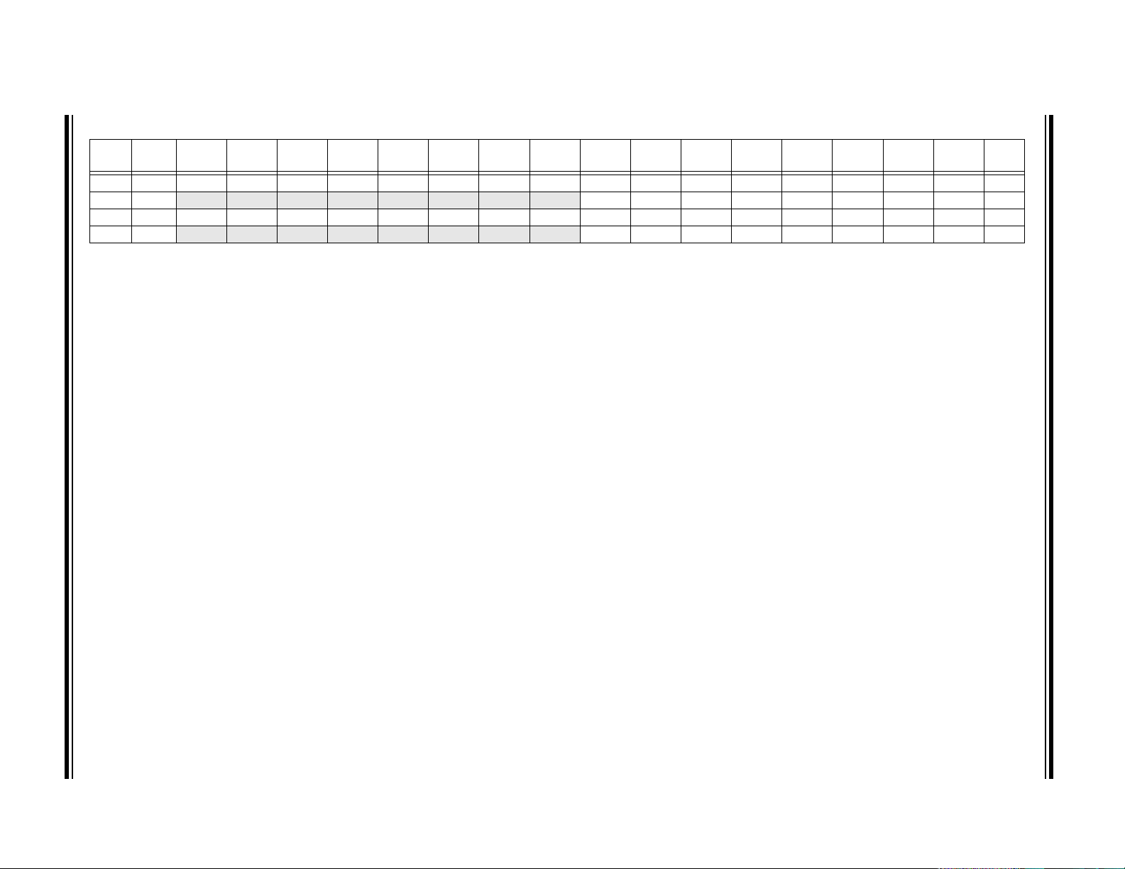
© 2007 Microchip Technology Inc. Preliminary DS70165E-page 47
TABLE 3-2: CHANGE NOTIFICATION REGISTER MAP
SFR
Name
CNEN1 0060 CN15IE CN14IE CN13IE CN12IE CN11IE CN10IE CN9IE CN8IE CN7IE CN6IE CN5IE CN4IE CN3IE CN2IE CN1IE CN0IE
CNEN2 0062
CNPU1 0068 CN15PUE CN14PUE CN13PUE CN12PUE CN1 1PUE CN10PUE CN9PUE CN8PUE CN7PUE CN6PUE CN5PUE CN4PUE CN3PUE CN2PUE CN1PUE CN0PUE
CNPU2 006A
Legend: x = unknown value on Reset, — = unimplemented, read as ‘0’. Reset values are shown in hexadecimal.
SFR
Addr
Bit 15 Bit 14 Bit 13 Bit 12 Bit 11 Bit 10 Bit 9 Bit 8 Bit 7 Bit 6 Bit 5 Bit 4 Bit 3 Bit 2 Bit 1 Bit 0
— — — — — — — —
— — — — — — — —
CN23IE CN22IE CN21IE CN20IE CN19IE CN18IE CN17IE CN16IE
CN23PUE CN22PUE CN21PUE CN20PUE CN19PUE CN18PUE CN17PUE CN16PUE
All
Resets
0000
0000
0000
0000
dsPIC33F
Page 50
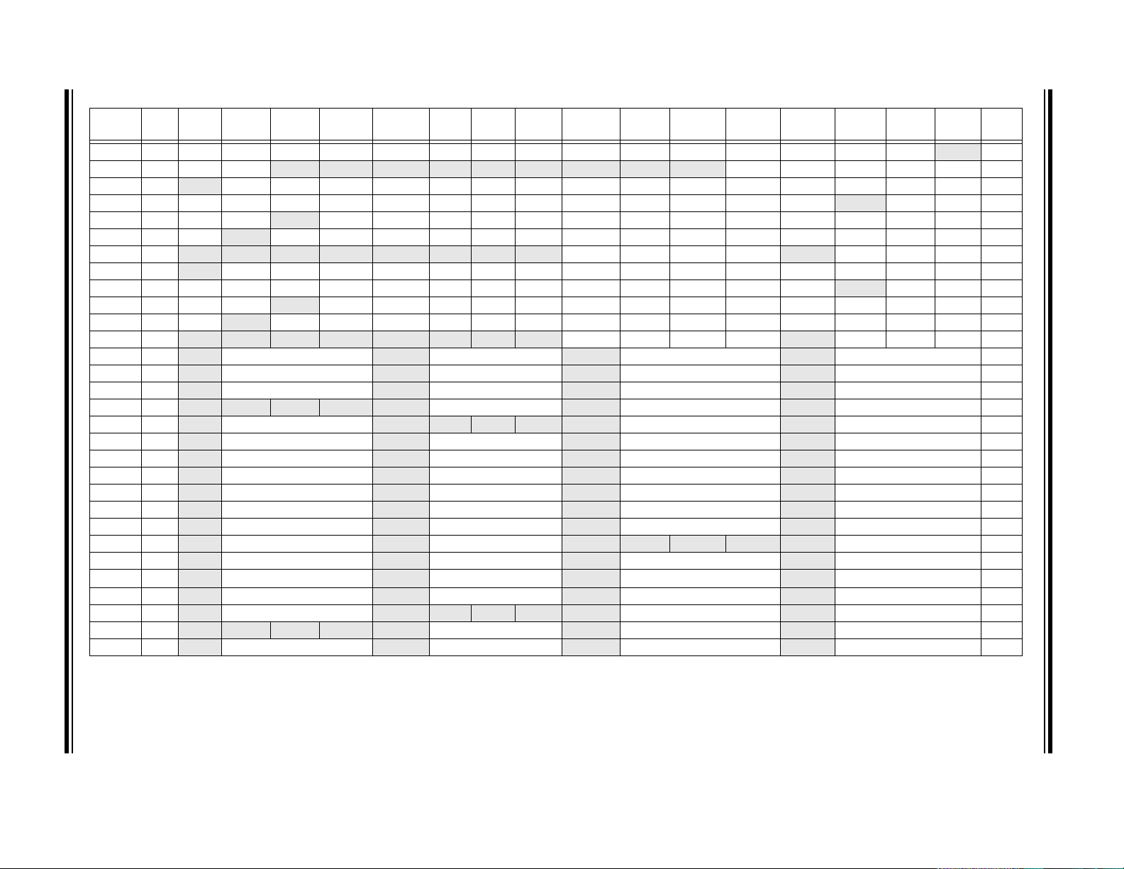
DS70165E-page 48 Preliminary © 2007 Microchip Technology Inc.
dsPIC33F
TABLE 3-3: INTERRUPT CONTROLLER REGISTER MAP
SFR
Name
INTCON1 0080 NSTDIS OV AERR OVBERR COVAERR COVBERR OVATE OVBTE COVTE SFT ACE RR DIV0ERR DMACERR MATHERR ADDRERR STKERR OSCFAIL
INTCON2 0082 ALTIVT DISI
IFS0 0084
IFS1 0086 U2TXIF U2RXIF INT2IF T5IF T4IF OC4IF OC3IF DMA2IF IC8IF IC7IF AD2IF INT1IF CNIF
IFS2 0088 T6IF DMA4IF
IFS3 008A FLTAIF
IFS4 008C
IEC0 0094
IEC1 0096 U2TXIE U2RXIE INT2IE T5IE T4IE OC4IE OC3IE DMA2IE IC8IE IC7IE AD2IE INT1IE CNIE
IEC2 0098 T6IE DMA4IE
IEC3 009A FLTAIE
IEC4 009C
IPC0 00A4
IPC1 00A6
IPC2 00A8
IPC3 00AA
IPC4 00AC
IPC5 00AE
IPC6 00B0
IPC7 00B2
IPC8 00B4
IPC9 00B6
IPC10 00B8
IPC11 00BA
IPC12 00BC
IPC13 00BE
IPC14 00C0
IPC15 00C2
IPC16 00C4
IPC17 00C6
Legend: x = unknown value on Reset, — = unimplemented, read as ‘0’. Reset values are shown in hexadecimal.
SFR
Bit 15 Bit 14 Bit 13 Bit 12 Bit 11 Bit 10 Bit 9 Bit 8 Bit 7 Bit 6 Bit 5 Bit 4 Bit 3 Bit 2 Bit 1 Bit 0
Addr
— — — — — — — — — INT4EP INT3EP INT2EP INT1EP INT0EP 0000
— DMA1IF AD1IF U1TXIF U1RXIF SPI1IF SPI1EIF T3IF T2IF OC2IF IC2IF DMA0IF T1IF OC1IF IC1IF INT0IF 0000
— MI2C1IF SI2C1IF 0000
— OC8IF OC7IF OC6IF OC5IF IC6IF IC5IF IC4IF IC3IF DMA3IF C1IF C1RXIF SPI2IF SPI2EIF 0000
— DMA5IF DCIIF DCIEIF QEIIF PWMIF C2IF C2RXIF INT4IF INT3IF T9IF T8IF MI2C2IF SI2C2IF T7IF 0000
— — — — — — — — C2TXIF C1TXIF DMA7IF DMA6IF — U2EIF U1EIF FLTBIF 0000
— DMA1IE AD1IE U1TXIE U1RXIE SPI1IE SPI1EIE T3IE T2IE OC2IE IC2IE DMA0IE T1IE OC1IE IC1IE INT0IE 0000
— MI2C1IE SI2C1IE 0000
— OC8IE OC7IE OC6IE OC5IE IC6IE IC5IE IC4IE IC3IE DMA3IE C1IE C1RXIE SPI2IE SPI2EIE 0000
— DMA5IE DCIIE DCIEIE QEIIE PWMIE C2IE C2RXIE INT4IE INT3IE T9IE T8IE MI2C2IE SI2C2IE T7IE 0000
— — — — — — — — C2TXIE C1TXIE DMA7IE DMA6IE — U2EIE U1EIE FLTBIE 0000
— T1IP<2:0> —OC1IP<2:0>—IC1IP<2:0>— INT0IP<2:0> 4444
— T2IP<2:0> —OC2IP<2:0>—IC2IP<2:0>— DMA0IP<2:0> 4444
— U1RXIP<2:0> — SPI1IP<2:0> — SPI1EIP<2:0> — T3IP<2:0> 4444
— — — — — DMA1IP<2:0> — AD1IP<2:0> — U1TXIP<2:0> 4444
— CNI P<2:0> — — — — — MI2C1IP<2:0> — SI2C1IP<2:0> 4444
— IC8IP<2:0> —IC7IP<2:0>— AD2IP<2:0> — INT1IP<2:0> 4444
— T4IP<2:0> —OC4IP<2:0>—OC3IP<2:0>— DMA2IP<2:0> 4444
— U2TXIP<2:0> — U2RXIP<2:0> — INT2IP<2:0> — T5IP<2:0> 4444
— C1IP<2:0> — C1RXIP<2:0> — SPI2IP<2:0> — SPI2EIP<2:0> 4444
— IC5IP<2:0> —IC4IP<2:0>—IC3IP<2:0>— DMA3IP<2:0> 4444
— OC7IP<2:0> —OC6IP<2:0>—OC5IP<2:0>—IC6IP<2:0>4444
— T6IP<2:0> — DMA4IP<2:0> — — — — — OC8IP<2:0> 4444
— T8IP<2:0> — MI2C2IP<2:0> — SI2C2IP<2:0> — T7IP<2:0> 4444
— C2RXIP<2:0> — INT4IP<2:0> — INT3IP<2:0> — T9IP<2:0> 4444
— DCIEIP<2:0> —QEIIP<2:0>—PWMIP<2:0>— C2IP<2:0> 4444
— FLTAIP<2:0> — — — — — DMA5IP<2:0> — DCIIP<2:0> 4444
— — — — — U2EIP<2:0> — U1EIP<2:0> — FLTBIP<2:0> 4444
— C2TXIP<2:0> — C1TXIP<2:0> — DMA7IP<2:0> — DMA6IP<2:0> 4444
All
Resets
— 0000
Page 51
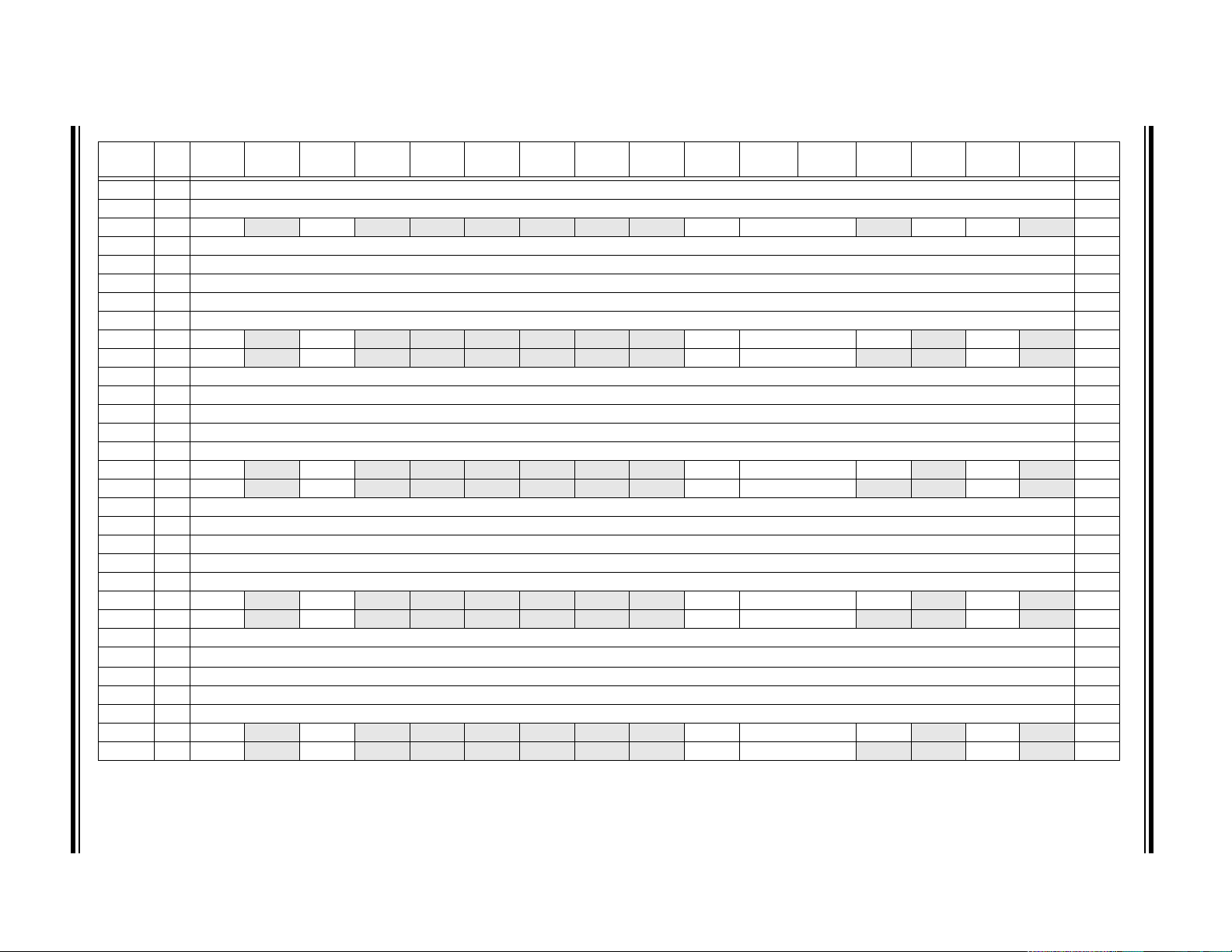
© 2007 Microchip Technology Inc. Preliminary DS70165E-page 49
TA BLE 3-4: TIMER REGISTER MAP
SFR
SFR
Name
TMR1 0100 Timer1 R egi ster
PR1 0102 Period Register 1
T1CON 0104 TON
TMR2 0106 Timer2 R egi ster
TMR3HLD 0108 Timer3 Ho ldin g Re gis ter (for 3 2- bit timer op eration s on ly)
TMR3 010A Timer3 Register
PR2 010C Period Register 2
PR3 010E Period Register 3
T2CON 0110 TON
T3CON 0112 TON
TMR4 0114 Timer4 R egi ster
TMR5HLD 0 116 Timer5 Ho lding Reg ister (for 32-bit op erations on ly)
TMR5 0118 Timer5 R egi ster
PR4 011A Period Register 4
PR5 01 1C Period Register 5
T4CON 011E TON
T5CON 0120 TON
TMR6 0122 Timer6 R egi ster
TMR7HLD 0124 T imer7 Holding R egiste r (for 32-bit opera tions only)
TMR7 0126 Timer7 R egi ster
PR6 0128 Period Register 6
PR7 012A Period Register 7
T6CON 012C TON —TSIDL— — — — — — TGATE TCKPS<1:0> T32 —TCS
T7CON 012E TON —TSIDL— — — — — — TGATE TCKPS<1:0> — —TCS
TMR8 0130 Timer8 R egi ster
TMR9HLD 0132 T imer9 Holding R egiste r (for 32-bit opera tions only)
TMR9 0134 Timer9 R egi ster
PR8 0136 Period Register 8
PR9 0138 Period Register 9
T8CON 013A TON
T9CON 013C TON
Legend: x = unknown value on Reset, — = unimplemented, read as ‘0’. Reset values are shown in hexadecimal.
Bit 15 Bit 14 Bit 13 Bit 12 Bit 11 Bit 10 Bit 9 Bit 8 Bit 7 Bit 6 Bit 5 Bit 4 Bit 3 Bit 2 Bit 1 Bit 0
Addr
—
TSIDL
—
TSIDL
—
TSIDL
—
TSIDL
—
TSIDL
—
TSIDL
—
TSIDL
— — — — — —
— — — — — —
— — — — — —
— — — — — —
— — — — — —
— — — — — —
— — — — — —
TGA TE TCKPS<1:0>
TGA TE TCKPS<1:0> T32
TGA TE TCKPS<1:0>
TGA TE TCKPS<1:0> T32
TGA TE TCKPS<1:0>
TGA TE TCKPS<1:0> T32
TGA TE TCKPS<1:0>
—
— —
— —
— —
TSYNC TCS
—
—
—
TCS
TCS
TCS
TCS
TCS
TCS
All
Resets
xxxx
FFFF
—
0000
xxxx
xxxx
xxxx
FFFF
FFFF
—
0000
—
0000
xxxx
xxxx
xxxx
FFFF
FFFF
—
0000
—
0000
xxxx
xxxx
xxxx
FFFF
FFFF
—
0000
—
0000
xxxx
xxxx
xxxx
FFFF
FFFF
—
0000
—
0000
dsPIC33F
Page 52
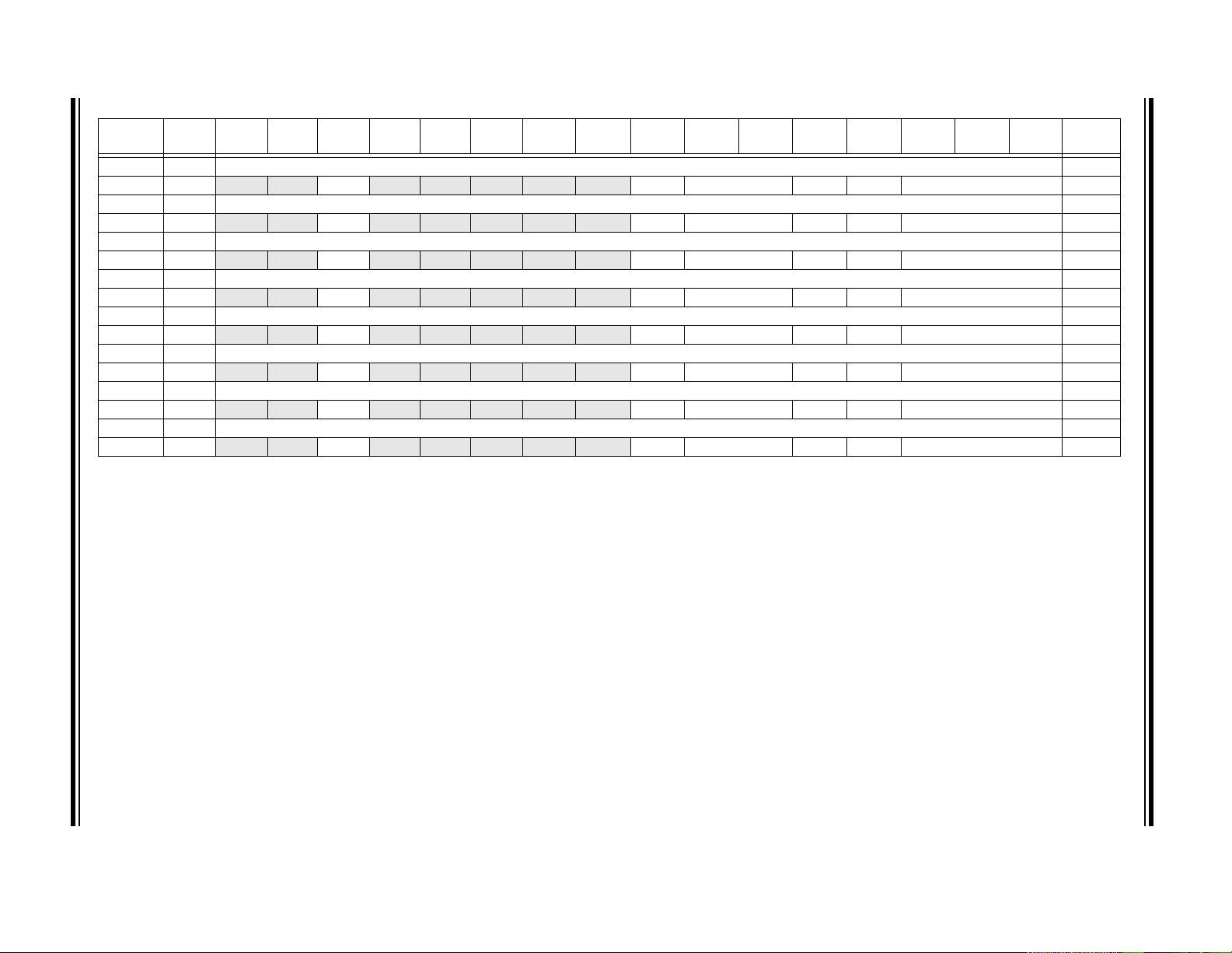
DS70165E-page 50 Preliminary © 2007 Microchip Technology Inc.
dsPIC33F
TABLE 3-5: INPUT CAPTURE REGISTER MAP
SFR Name
IC1BUF 0140 Input 1 Capture Re gister
IC1CON 0142
IC2BUF 0144 Input 2 Capture Re gister
IC2CON 0146
IC3BUF 0148 Input 3 Capture Re gister
IC3CON 014A
IC4BUF 014C Input 4 Capture Re gister
IC4CON 014E
IC5BUF 0150 Input 5 Capture Re gister
IC5CON 0152
IC6BUF 0154 Input 6 Capture Re gister
IC6CON 0156
IC7BUF 0158 Input 7 Capture Re gister
IC7CON 015A
IC8BUF 015C Input 8 Capture Re gister
IC8CON 015E
Legend: x = unknown value on Reset, — = unimplemented, read as ‘0’. Reset values are shown in hexadecimal.
SFR
Addr
Bit 15 Bit 14 Bit 13 Bit 12 Bit 11 Bit 10 Bit 9 Bit 8 Bit 7 Bit 6 Bit 5 Bit 4 Bit 3 Bit 2 Bit 1 Bit 0
— —
— —
— —
— —
— —
— —
— —
— —
ICSIDL
ICSIDL
ICSIDL
ICSIDL
ICSIDL
ICSIDL
ICSIDL
ICSIDL
— — — — —
— — — — —
— — — — —
— — — — —
— — — — —
— — — — —
— — — — —
— — — — —
ICTMR ICI<1:0> ICOV ICBNE ICM<2:0>
ICTMR ICI<1:0> ICOV ICBNE ICM<2:0>
ICTMR ICI<1:0> ICOV ICBNE ICM<2:0>
ICTMR ICI<1:0> ICOV ICBNE ICM<2:0>
ICTMR ICI<1:0> ICOV ICBNE ICM<2:0>
ICTMR ICI<1:0> ICOV ICBNE ICM<2:0>
ICTMR ICI<1:0> ICOV ICBNE ICM<2:0>
ICTMR ICI<1:0> ICOV ICBNE ICM<2:0>
All
Resets
xxxx
0000
xxxx
0000
xxxx
0000
xxxx
0000
xxxx
0000
xxxx
0000
xxxx
0000
xxxx
0000
Page 53
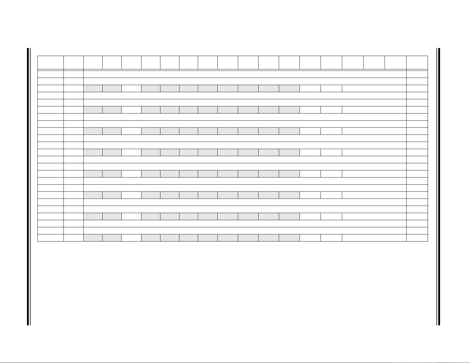
© 2007 Microchip Technology Inc. Preliminary DS70165E-page 51
TABLE 3-6: OUTPUT COMPARE REGISTER MAP
SFR Name
OC1RS 0180 Output Compare 1 Secondary Register
OC1R 0182 Output Compar e 1 R e gister
OC1CON 0184
OC2RS 0186 Output Compare 2 Secondary Register
OC2R 0188 Output Compar e 2 R e gister
OC2CON 018A
OC3RS 018C Output Compa re 3 Secon dary Re gister
OC3R 018E O utpu t Co m p ar e 3 R e gister
OC3CON 0190
OC4RS 0192 Output Compare 4 Secondary Register
OC4R 0194 Output Compar e 4 R e gister
OC4CON 0196
OC5RS 0198 Output Compare 5 Secondary Register
OC5R 019A O utpu t Co m p ar e 5 R e gister
OC5CON 019C
OC6RS 019E Output Compare 6 Secondary Register
OC6R 01A0 O utpu t Co m p are 6 R egi ster
OC6CON 01A2
OC7RS 01A4 Output Compare 7 Secondary Register
OC7R 01A6 O utpu t Co m p are 7 R egi ster
OC7CON 01A8
OC8RS 01AA Output Compare 8 Secondary Register
OC8R 01AC Output Comp ar e 8 R e gister
OC8CON 01A E
Legend: x = unknown value on Reset, — = unimplemented, read as ‘0’. Reset values are shown in hexadecimal.
SFR
Addr
Bit 15 Bit 14 Bit 13 Bit 12 Bit 11 Bit 10 Bit 9 Bit 8 Bit 7 Bit 6 Bit 5 Bit 4 Bit 3 Bit 2 Bit 1 Bit 0
— —
— —
— —
— —
— —
— —
— —
— —
OCSIDL
OCSIDL
OCSIDL
OCSIDL
OCSIDL
OCSIDL
OCSIDL
OCSIDL
— — — — — — — —
— — — — — — — —
— — — — — — — —
— — — — — — — —
— — — — — — — —
— — — — — — — —
— — — — — — — —
— — — — — — — —
OCFL T OCTSEL OCM<2:0>
OCFL T OCTSEL OCM<2:0>
OCFL T OCTSEL OCM<2:0>
OCFL T OCTSEL OCM<2:0>
OCFL T OCTSEL OCM<2:0>
OCFL T OCTSEL OCM<2:0>
OCFL T OCTSEL OCM<2:0>
OCFL T OCTSEL OCM<2:0>
All
Resets
xxxx
xxxx
0000
xxxx
xxxx
0000
xxxx
xxxx
0000
xxxx
xxxx
0000
xxxx
xxxx
0000
xxxx
xxxx
0000
xxxx
xxxx
0000
xxxx
xxxx
0000
dsPIC33F
Page 54
DS70165E-page 52 Preliminary © 2007 Microchip Technology Inc.
dsPIC33F
TABLE 3-7: 8-OUTPUT PWM REGISTER MAP
SFR Name Addr. Bit 15 Bit 14 Bit 13 Bit 12 Bit 11 Bit 10 Bit 9 Bit 8 Bit 7 Bit 6 Bit 5 Bit 4 Bit 3 Bit 2 Bit 1 Bit 0 Reset State
PTCON 01C0 PTEN
PTMR 01C2 PTDIR PWM Timer Count Value Register
PTPER 01C4 — PWM Time Base Period Register
SEVTCMP 01C6 SEVTDI
PWMCON1
PWMCON2
DTCON1 01CC DTBPS<1:0> DTB<5:0> DTAPS<1 :0> DTA<5 :0>
DTCON2 01CE — — — — — — — — DTS4A DTS4I DTS3A DTS3I DTS2A DTS2I DTS1A DTS1I
FLTACON 01D0 F A OV 4H FAOV4L FAOV3HFAOV3L FAOV2HFAOV2L FAOV1HFAOV1L FLTAM — — — FAEN4 FAEN3 FAEN2 F AE N1
01C8 — — — — PMOD4 PMOD3 PM OD2 PMOD1 PEN4H PEN3H PEN2H PEN1H PEN4L PEN3L PEN2L PEN1L
01CA — — — — SEVOPS<3:0> — — — — — IUE OSYNC UDIS
R
—PTSIDL— — — — — PTOPS<3:0> PTCKPS<1:0> PTMOD<1:0>
PWM Special Event Compare Register
0000 0000 0000 0000
0000 0000 0000 0000
0000 0000 0000 0000
0000 0000 0000 0000
0000 0000 1111 1111
0000 0000 0000 0000
0000 0000 0000 0000
0000 0000 0000 0000
0000 0000 0000 0000
FLTBCON 01D2 FBOV4H FBOV4L FBOV3HFBOV3L FBOV2HFBOV2L FBOV1HFBOV1L FLTBM — — — FBEN4 FBEN3 FBEN2 FBEN1
OVDCON 01D4 POVD4H POVD4LPOVD3HPOVD3LPOVD2HPOVD2L POVD1HPOVD1L POUT4HPOUT4LPOUT3HPOUT3LPOUT2HPOUT2LPOUT1HPOUT1
L
PDC1 01D6 PWM Duty Cycle #1 Register
PDC2 01D8 PWM Duty Cycle #2 Register
PDC3 01DA PWM Duty Cycle #3 Register
PDC4 01DC PWM Duty Cycle #4 Register
Legend: u = uninitialized bit, — = unimplemented, read as ‘0’
0000 0000 0000 0000
1111 1111 0000 0000
0000 0000 0000 0000
0000 0000 0000 0000
0000 0000 0000 0000
0000 0000 0000 0000
Page 55

© 2007 Microchip Technology Inc. Preliminary DS70165E-page 53
TABLE 3-8: QEI REGISTER MAP
SFR
Name
QEICON 01E0 CNTERR
DFLTCON 01E2
POSCNT 01E4 Position Counter<15:0> 0000 0000 0000 0000
MAXCNT 01E6 Maximum Count<15:0> 1111 1111 1111 1111
Legend: u = uninitialized bit, — = unimplemented, read as ‘0’
Addr
Bit 15 Bit 14 Bit 13 Bit 12 Bit 11 Bit 10 Bit 9 Bit 8 Bit 7 Bit 6 Bit 5 Bit 4 Bit 3 Bit 2 Bit 1 Bit 0 Reset State
.
— QEISIDL INDX UPDN QEIM<2:0> SWPAB PCDOUT TQGATE TQCKPS<1:0> POSRES TQCS UPDN_SRC 0000 0000 0000 0000
— — — — — IMV<1:0> CEID QEOUT QECK<2:0> — — — — 0000 0000 0000 0000
TABLE 3-9: I2C1 REGISTER MAP
SFR Name
I2C1RCV 0200 — — — — — — — — Receive Register
I2C1 T R N 0202 — — — — — — — — Transmit Register
I2C1BRG 0204 — — — — — — — Baud Rate Generator Register
I2C1CON 0206 I2CEN — I2CSIDL SCLREL IPMIEN A10M DISSL W SMEN GCEN STREN ACKDT ACKEN RCEN PEN RSEN SEN
I2C1STA T 0208 ACKSTA T TRSTAT — — — BCL GCSTA T ADD10 IWCOL I2COV D_A P S R_W RBF TBF
I2C1ADD 020A — — — — — — Address Regis ter
I2C1MSK 020C — — — — — — Address M a sk Re g ist er
Legend: x = unknown value on Reset, — = unimplemented, read as ‘0’. Reset values are shown in hexadecimal.
SFR
Addr
Bit 15 Bit 14 Bit 13 Bit 12 Bit 11 Bit 10 Bit 9 Bit 8 Bit 7 Bit 6 Bit 5 Bit 4 Bit 3 Bit 2 Bit 1 Bit 0
All
Resets
0000
00FF
0000
1000
0000
0000
0000
TABLE 3-10: I2C2 REGISTER MAP
SFR Name
I2C2RCV 0210 — — — — — — — — Receive Register
I2C2TRN 0212 — — — — — — — — Transmit Register
I2C2BRG 0214 — — — — — — — Baud Rate Generator Reg ister
I2C2CON 0216 I2CEN — I2CSIDL SCLREL IPMIEN A10M DISSL W SMEN GCEN STREN ACKDT ACKEN RCEN PEN RSEN SEN
I2C2STA T 0218 ACKSTAT TRSTAT — — — BCL GCSTA T ADD10 IWCOL I2COV D_A P S R_W RBF TBF
I2C2ADD 021A — — — — — — Address Reg ister
I2C2MSK 021C — — — — — — Address Mask Register
Legend: x = unknown value on Reset, — = unimplemented, read as ‘0’. Reset values are shown in hexadecimal.
SFR
Addr
Bit 15 Bit 14 Bit 13 Bit 12 Bit 11 Bit 10 Bit 9 Bit 8 Bit 7 Bit 6 Bit 5 Bit 4 Bit 3 Bit 2 Bit 1 Bit 0
All
Resets
0000
00FF
0000
1000
0000
0000
0000
dsPIC33F
Page 56
DS70165E-page 54 Preliminary © 2007 Microchip Technology Inc.
dsPIC33F
TABLE 3-11: UART1 REGISTER MAP
SFR Name
U1MODE 0220 UARTEN — USIDL IREN RTSMD — UEN1 UEN0 WAKE LPBACK ABAUD URXINV BRGH PDSEL<1:0> STSEL
U1STA 0222 UTXISEL1 UTXINV UTXISEL0 — UTXBRK UTXEN UTXBF TRMT URXISEL<1:0> ADDEN RIDLE PERR FERR OERR URXDA
U1TXREG 0224 — — — — — — — UART Transm it R egist er
U1RXREG 0226 — — — — — — — UART Receive Re gister
U1BRG 0228 Baud R a te G en era to r P r es ca le r
Legend: x = unknown value on Reset, — = unimplemented, read as ‘0’. Reset values are shown in hexadecimal.
SFR
Addr
Bit 15 Bit 14 Bit 13 Bit 12 Bit 11 Bit 10 Bit 9 Bit 8 Bit 7 Bit 6 Bit 5 Bit 4 Bit 3 Bit 2 Bit 1 Bit 0
All
Resets
0000
0110
xxxx
0000
0000
TABLE 3-12: UART2 REGISTER MAP
SFR
Name
U2MODE 0230 UARTEN — USIDL IREN RTSMD — UEN1 UEN0 WAKE LPBACK ABAUD URXINV BRGH PDSEL<1:0> STSEL
U2STA 0232 UTXISEL1 UTXINV UTXISEL0 — UTXBRK UTXEN UTXBF TRMT URXISEL<1:0> ADDEN RIDLE PERR FERR OERR URXDA
U2TXREG 0234 — — — — — — — UART T r an smi t Re gister
U2RXREG 0236 — — — — — — — UART Receive Register
U2BRG 0238 Baud Rate Ge nerator P resca ler
Legend: x = unknown value on Reset, — = unimplemented, read as ‘0’. Reset values are shown in hexadecimal.
SFR
Addr
Bit 15 Bit 14 Bit 13 Bit 12 Bit 11 Bit 10 Bit 9 Bit 8 Bit 7 Bit 6 Bit 5 Bit 4 Bit 3 Bit 2 Bit 1 Bit 0
All
Resets
0000
0110
xxxx
0000
0000
TABLE 3-13: SPI1 REGISTER MAP
SFR
Name
SPI1STAT 0240 SPIEN — SPISIDL — — — — — — SPIROV — — — — SPITBF SPIRBF
SPI1CON1 0242 — — — DISSCK DISSDO MODE16 SMP CKE SSEN CKP MSTEN SPRE<2:0> PPRE<1:0>
SPI1CON2 0244 FRMEN SPIFSD FRMPOL — — — — — — — — — — —FRMDLY—
SPI1BUF 0248 SPI1 Transmit and Receive Buffer Register
Legend: x = unknown value on Reset, — = unimplemented, read as ‘0’. Reset values are shown in hexadecimal.
SFR
Addr
Bit 15 Bit 14 Bit 13 Bit 12 Bit 11 Bit 10 Bit 9 Bit 8 Bit 7 Bit 6 Bit 5 Bit 4 Bit 3 Bit 2 Bit 1 Bit 0
All
Resets
0000
0000
0000
0000
TABLE 3-14: SPI2 REGISTER MAP
SFR
SFR Name
SPI2STAT 0260 SPIEN —SPISIDL— — — — — — SPIROV — — — — SPITBF SPIRBF
SPI2CON1 0262 — — — DISSCK DISSDO MODE16 SMP CKE SSEN CKP MSTEN SPRE<2:0> PPRE<1:0>
SPI2CON2 0264 FRMEN SPIFSD FRMPOL — — — — — — — — — — — FRMDLY —
SPI2BUF 0268 SPI2 Transmit and Receive Buffer Register
Legend: x = unknown value on Reset, — = unimplemented, read as ‘0’. Reset values are shown in hexadecimal.
Bit 15 Bit 14 Bit 13 Bit 12 Bit 11 Bit 10 Bit 9 Bit 8 Bit 7 Bit 6 Bit 5 Bit 4 Bit 3 Bit 2 Bit 1 Bit 0
Addr
All
Resets
0000
0000
0000
0000
Page 57
© 2007 Microchip Technology Inc. Preliminary DS70165E-page 55
TABLE 3-15: ADC1 REGISTER MAP
File Name Addr Bit 15 Bit 14 Bit 13 Bit 12 Bit 11 Bit 10 Bit 9 Bit 8 Bit 7 Bit 6 Bit 5 Bit 4 Bit 3 Bit 2 Bit 1 Bit 0
ADC1BUF0 0300 ADC Data Buffer 0 xxxx
AD1CON1 0320 ADON
AD1CON2 0322 VCFG<2:0>
AD1CON3 0324 ADRC
AD1CHS123 0326
AD1CHS0 0328 CH0NB
AD1PCFGH 032A PCFG31 PCFG30 PCFG29 PCFG28 PCFG27 PCFG26 PCFG25 PCFG24 PCFG23 PCFG22 PCFG21 PCFG20 PCFG19 PCFG18 PCFG17 PCFG16 0000
AD1PCFGL 032C PCFG15 PCFG14 PCFG13 PCFG12 PCFG11 PCFG10 PCFG9 PCFG8 PCFG7 PCFG6 PCFG5 PCFG4 PCFG3 PCFG2 PCFG1 PCFG0 0000
AD1CSSH 032E CSS31 CSS30 CSS29 CSS28 CSS27 CSS26 CSS25 CSS24 CSS23 CSS22 CSS21 CSS20 CSS19 CSS18 CSS17 CSS16 0000
AD1CSSL 0330 CSS15 CSS14 CSS1 3 CSS12 CSS11 C SS10 CSS9 CSS8 CSS7 CSS6 CSS5 CSS4 CSS3 CSS2 CSS1 CSS0 0000
AD1CON4 0332
Legend: x = unknown value on Reset, — = unimplemented, read as ‘0’. Reset values are shown in hexadecimal.
— — — — — CH123NB<1:0> CH123SB — — — — — CH123NA<1:0> CH123SA 0000
— — — — — — — — — — — — — DMABL<2:0> 0000
— ADSIDL ADDMABM — AD12B FORM<1:0> SSRC<2:0> — SIMSAM ASAM SAMP DONE 0000
— — CSCNA CHPS<1:0> BUFS — SMPI<3:0> BUFM ALTS 0000
— — SAMC<4:0> — — ADCS<5:0> 0000
— — CH0SB<4:0> CH0NA — — CH0SA<4:0> 0000
Resets
TABLE 3-16: ADC2 REGISTER MAP
File Name Addr Bit 15 Bit 14 Bit 13 Bit 12 Bit 11 Bit 10 Bit 9 Bit 8 Bit 7 Bit 6 Bit 5 Bit 4 Bit 3 Bit 2 Bit 1 Bit 0
ADC2BUF0 0340 ADC Data Buffer 0 xxxx
AD2CON1 0360 ADON
AD2CON2 0362 VCFG<2:0>
AD2CON3 0364 ADRC
AD2CHS123 0366
AD2CHS0 0368 CH0NB
Reserved 036A
AD2PCFGL 036C PCFG15 PCFG14 PCFG13 PCFG12 PCFG11 PCFG10 PCFG9 PCFG8 PCFG7 PCFG6 PCFG5 PCFG4 PCFG3 PCFG2 PCFG1 PCFG0 0000
Reserved 036E
AD2CSSL 0370 CSS15 CSS14 CSS13 CSS12 CSS11 CSS10 CSS9 CSS8 CSS7 CSS6 CSS5 C SS4 CSS3 CSS2 CSS1 CSS0 0000
AD2CON4 0372
Legend: x = unknown value on Reset, — = unimplemented, read as ‘0’. Reset values are shown in hexadecimal.
— — — — — CH123NB<1:0> CH123SB — — — — — CH123NA<1:0> CH123SA 0000
— — — — — — — — — — — — — — — — 0000
— — — — — — — — — — — — — — — — 0000
— — — — — — — — — — — — — DMABL<2:0> 0000
— ADSIDL ADDMABM — AD12B FORM<1:0> SSRC<2:0> — SIMSAM ASAM SAMP DONE 0000
— — CSCNA CHPS<1:0> BUFS — SMPI<3:0> BUFM ALTS 0000
— — SAMC<4:0> — — ADCS<5:0> 0000
— — — CH0SB<3:0> CH0NA — — — CH0SA<3:0> 0000
All
Resets
All
dsPIC33F
Page 58

DS70165E-page 56 Preliminary © 2007 Microchip Technology Inc.
TABLE 3-17: DMA REGISTER MAP
File Name Addr Bit 15 Bit 14 Bit 13 Bit 12 Bit 11 Bit 10 Bit 9 Bit 8 Bit 7 Bit 6 Bit 5 Bit 4 Bit 3 Bit 2 Bit 1 Bit 0
DMA0CON 0380 CHEN SIZE DIR HALF NULLW
DMA0REQ 0382 FORCE
DMA0STA 0384 STA<15:0> 0000
DMA0STB 0386 STB<15:0> 0000
DMA0PAD 0388 PAD<15:0> 0000
DMA0CNT 038A
DMA1CON 038C CHEN SIZE DIR HALF NULLW
DMA1REQ 038E FORCE
DMA1STA 0390 STA<15:0> 0000
DMA1STB 0392 STB<15:0> 0000
DMA1PAD 0394 PAD<15:0> 0000
DMA1CNT 0396
DMA2CON 0398 CHEN SIZE DIR HALF NULLW
DMA2REQ 039A FORCE
DMA2STA 039C STA<15:0> 0000
DMA2STB 039E STB<15:0> 0000
DMA2PAD 03A0 PAD<15:0> 0000
DMA2CNT 03A2
DMA3CON 03A4 CHEN SIZE DIR HALF NULLW
DMA3REQ 03A6 FORCE
DMA3STA 03A8 STA<15:0> 0000
DMA3STB 03AA STB<15:0> 0000
DMA3PAD 03AC PAD<15:0> 0000
DMA3CNT 03AE
DMA4CON 03B0 CHEN SIZE DIR HALF NULLW
DMA4REQ 03B2 FORCE
DMA4STA 03B4 STA<15:0> 0000
DMA4STB 03B6 STB<15:0> 0000
DMA4PAD 03B8 PAD<15:0> 0000
DMA4CNT 03BA
DMA5CON 03BC CHEN SIZE DIR HALF NULLW
DMA5REQ 03BE FORCE
DMA5STA 03C0 STA<15:0> 0000
DMA5STB 03C2 STB<15:0> 0000
DMA5PAD 03C4 PAD<15:0> 0000
Legend: — = unimplemented, read as ‘0’. Reset values are shown in hexadecimal.
— — — — — — CNT<9:0> 0000
— — — — — — CNT<9:0> 0000
— — — — — — CNT<9:0> 0000
— — — — — — CNT<9:0> 0000
— — — — — — CNT<9:0> 0000
— — — — — — — — IRQSEL<6:0> 0000
— — — — — — — — IRQSEL<6:0> 0000
— — — — — — — — IRQSEL<6:0> 0000
— — — — — — — — IRQSEL<6:0> 0000
— — — — — — — — IRQSEL<6:0> 0000
— — — — — — — — IRQSEL<6:0> 0000
— — — — —AMODE<1:0>— —MODE<1:0>0000
— — — — —AMODE<1:0>— —MODE<1:0>0000
— — — — —AMODE<1:0>— —MODE<1:0>0000
— — — — —AMODE<1:0>— —MODE<1:0>0000
— — — — —AMODE<1:0>— —MODE<1:0>0000
— — — — —AMODE<1:0>— —MODE<1:0>0000
All
Resets
dsPIC33F
Page 59

© 2007 Microchip Technology Inc. Preliminary DS70165E-page 57
TABLE 3-17: DMA REGISTER MAP (CONTINUED)
File Name Addr Bit 15 Bit 14 Bit 13 Bit 12 Bit 11 Bit 10 Bit 9 Bit 8 Bit 7 Bit 6 Bit 5 Bit 4 Bit 3 Bit 2 Bit 1 Bit 0
DMA5CNT 03C6 — — — — — — CNT<9:0> 0000
DMA6CON 03C8 CHEN SIZE DIR HALF NULLW
DMA6REQ 03CA FORCE
DMA6STA 03CC STA<15:0> 0000
DMA6STB 03CE STB<15:0> 0000
DMA6PAD 03D0 PAD<15:0> 0000
DMA6CNT 03D2
DMA7CON 03D4 CHEN SIZE DIR HALF NULLW
DMA7REQ 03D6 FORCE
DMA7STA 03D8 STA<15:0> 0000
DMA7STB 03DA STB<15:0> 0000
DMA7PAD 03DC PAD<15:0> 0000
DMA7CNT 03DE
DMACS0 03E0 PWCOL7 PWCOL6 PWCOL5 PWCOL4 PWCOL3 PWCOL2 PWCOL1 PWCOL0 XWCOL7 XWCOL6 XWCOL5 XWCOL4 XWCOL3 XWCOL2 XWCOL1 XWCOL0 0000
DMACS1 03E2
DSADR 03E4 DSADR<15:0> 0000
Legend: — = unimplemented, read as ‘0’. Reset values are shown in hexadecimal.
— — — — — — CNT<9:0> 0000
— — — — — — CNT<9:0> 0000
— — — — LSTCH<3:0> PPST7 PPST6 PPST5 PPST4 PPST3 PPST2 PPST1 PPST0 0000
— — — — — — — — IRQSEL<6:0> 0000
— — — — — — — — IRQSEL<6:0> 0000
— — — — —AMODE<1:0>— —MODE<1:0>0000
— — — — —AMODE<1:0>— —MODE<1:0>0000
All
Resets
dsPIC33F
Page 60

DS70165E-page 58 Preliminary © 2007 Microchip Technology Inc.
dsPIC33F
TABLE 3-18: ECAN1 REGISTER MAP WHEN C1CTRL1.WIN = 0 OR 1
File Name Addr Bit 15 Bit 14 Bit 13 Bit 12 Bit 11 Bit 10 Bit 9 Bit 8 Bit 7 Bit 6 Bit 5 Bit 4 Bit 3 Bit 2 Bit 1 Bit 0
C1CTRL1 0400
C1CTRL2 0402
C1VEC 0404
C1FCTRL 0406 DMABS<2:0>
C1FIFO 0408
C1INTF 040A
C1INTE 040C
C1EC 040E TERRCNT<7:0> RERRCNT<7:0> 0000
C1CFG1 0410
C1CFG2 0412
— — CSIDL ABAT CANCK
S
— — — — — — — — — — — DNCNT<4:0> 0000
— — —FILHIT<4:0> — ICODE<6:0> 0000
— — — — — — — —
— —FBP<5:0> — — FNRB<5:0> 0000
— — TXBO TXBP RXBP TXWAR RXWAR EWARN IVRIF WAKIF ERRIF — FIFOIF RBOVIF RBIF TBIF 0000
— — — — — — — — IVRIE WAKIE ERRIE — FIFOIE RBOVIE RBIE TBIE 0000
— — — — — — — — SJW<1:0> BRP<5:0> 0000
— WAKFIL — — — SEG2PH<2:0> SEG2PHTSSAM SEG1PH<2:0> PRSEG<2:0> 0000
REQOP<2:0> OPMODE<2:0> — CANCAP — —WIN0480
FSA<4:0>
All
Reset
s
0000
C1FEN1 0414
C1FMSKSEL1 0418 F7MSK<1:0> F6MSK<1:0> F5MSK<1:0> F4MSK<1:0> F3MSK<1:0> F2MSK<1:0> F1MSK<1:0> F0MSK<1:0> 0000
C1FMSKSEL2 041A F15MSK<1:0> F14MSK<1:0> F13MSK<1:0> F12MSK<1:0> F11MSK<1:0> F10MSK<1:0> F9MSK<1:0> F8MSK<1:0> 0000
Legend: — = unimplemented, read as ‘0’. Reset values are shown in hexadecimal.
FLTEN15 FL TEN1 4 FLTEN13 FLTEN12 FLTEN11 FLTEN10 FLTEN9 FLTEN8 FLTEN7 FLTEN6 FLTEN5 FLTEN4 FLTEN3 FLTEN2 FLTEN1 FLTEN0
0000
TABLE 3-19: ECAN1 REGISTER MAP WHEN C1CTRL1.WIN = 0
File Name Addr Bit 15 Bit 14 Bit 13 Bit 12 Bit 11 Bit 10 Bit 9 Bit 8 Bit 7 Bit 6 Bit 5 Bit 4 Bit 3 Bit 2 Bit 1 Bit 0
0400-
041E
C1RXFUL1 0420 RXFUL15 RXFUL14 RXFUL13 RXFUL12 RXFUL11 RXFUL10 RXFUL9 RXFUL8 RXFUL7 RXFUL6 RXFUL5 RXFUL4 RXFUL3 RXFUL2 RXFUL1 RXFUL0 0000
C1RXFUL2 0422 RXFUL31 RXFUL30 RXFUL29 RXFUL28 RXFUL27 RXFUL26 RXFUL25 RXFUL24 RXFUL23 RXFUL22 RXFUL21 RXFUL20 RXFUL19 RXFUL18 RXFUL17 RXFUL16 0000
C1RXOVF1 0428 RXOVF15 RXOVF14 RXOVF13 RXOVF12 RXOVF11 RXOVF10 RXOVF9 RXOVF8 RXOVF7 RXOVF6 RXOVF5 RXOVF4 RXOVF3 RXOVF2 RXOVF1 RXOVF0 0000
C1RXOVF2 042A RXOVF3 1 RXOVF30 RXOVF29 RXOVF28 RXOVF27 RXOVF26 RXOVF25 RXOVF24 RXOVF23 RXOVF22 RXOVF21 RXOVF20 RXOVF19 RXOVF18 RXOVF17 RXOVF16 0000
C1TR01CON 0430
C1TR23CON 0432
C1TR45CON 0434
C1TR67CON 0436
C1RXD 0440 Received Data Word xxxx
C1TXD 0442 Transmit Data Word xxxx
Legend: x = unknown value on Reset, — = unimplemented, read as ‘0’. Reset values are shown in hexadecimal.
TXEN1 TXABT1 TXLARB1 TXERR1 TXREQ1 RTREN1 TX1PRI<1:0> TXEN0 TXABAT0 TXLARB0 TXERR0 TXREQ0 RTREN0 TX0PRI<1:0>
TXEN3 TXABT3 TXLARB3 TXERR3 TXREQ3 RTREN3 TX3PRI<1:0> TXEN2 TXABAT2 TXLARB2 TXERR2 TXREQ2 RTREN2 TX2PRI<1:0>
TXEN5 TXABT5 TXLARB5 TXERR5 TXREQ5 RTREN5 TX5PRI<1:0> TXEN4 TXABAT4 TXLARB4 TXERR4 TXREQ4 RTREN4 TX4PRI<1:0>
TXEN7 TXABT7 TXLARB7 TXERR7 TXREQ7 RTREN7 TX7PRI<1:0> TXEN6 TXABAT6 TXLARB6 TXERR6 TXREQ6 RTREN6 TX6PRI<1:0>
See definition when WIN = x
All
Resets
0000
0000
0000
xxxx
Page 61

© 2007 Microchip Technology Inc. Preliminary DS70165E-page 59
TABLE 3-20: ECAN1 REGISTER MAP WHEN C1CTRL1.WIN = 1
File Name Addr Bit 15 Bit 14 Bit 13 Bit 12 Bit 11 Bit 10 Bit 9 Bit 8 Bit 7 Bit 6 Bit 5 Bit 4 Bit 3 Bit 2 Bit 1 Bit 0
0400-
041E
C1BUFPNT1 0420 F3BP<3:0> F2BP<3:0> F1BP<3:0> F0BP<3:0> 0000
C1BUFPNT2 0422 F7BP<3:0> F6BP<3:0> F5BP<3:0> F4BP<3:0> 0000
C1BUFPNT3 0424 F11BP<3:0> F10BP<3:0> F9BP<3:0> F8BP<3:0> 0000
C1BUFPNT4 0426 F15BP<3:0> F14BP<3:0> F13BP<3:0> F12BP<3:0> 0000
C1RXM0SID 0430 SID<10:3> SID<2:0>
C1RXM0EID 0432 EID<15:8> EID<7:0> xxxx
C1RXM1SID 0434 SID<10:3> SID<2:0>
C1RXM1EID 0436 EID<15:8> EID<7:0> xxxx
C1RXM2SID 0438 SID<10:3> SID<2:0>
C1RXM2EID 043A EID<15:8> EID<7:0> xxxx
C1RXF0SID 0440 SID<10:3> SID<2:0>
C1RXF0EID 0442 EID<15:8> EID<7:0> xxxx
C1RXF1SID 0444 SID<10:3> SID<2:0>
C1RXF1EID 0446 EID<15:8> EID<7:0> xxxx
C1RXF2SID 0448 SID<10:3> SID<2:0>
C1RXF2EID 044A EID<15:8> EID<7:0> xxxx
C1RXF3SID 044C SID<10:3> SID<2:0>
C1RXF3EID 044E EID<15:8> EID<7:0> xxxx
C1RXF4SID 0450 SID<10:3> SID<2:0>
C1RXF4EID 0452 EID<15:8> EID<7:0> xxxx
C1RXF5SID 0454 SID<10:3> SID<2:0>
C1RXF5EID 0456 EID<15:8> EID<7:0> xxxx
C1RXF6SID 0458 SID<10:3> SID<2:0>
C1RXF6EID 045A EID<15:8> EID<7:0> xxxx
C1RXF7SID 045C SID<10:3> SID<2:0>
C1RXF7EID 045E EID<15:8> EID<7:0> xxxx
C1RXF8SID 0460 SID<10:3> SID<2:0>
C1RXF8EID 0462 EID<15:8> EID<7:0> xxxx
C1RXF9SID 0464 SID<10:3> SID<2:0>
C1RXF9EID 0466 EID<15:8> EID<7:0> xxxx
C1RXF10SID 0468 SID<10:3> SID<2:0>
C1RXF10EID 046A EID<15:8> EID<7:0> xxxx
Legend: x = unknown value on Reset, — = unimplemented, read as ‘0’. Reset values are shown in hexadecimal.
See definition when WIN = x
—MIDE—EID<17:16>xxxx
—MIDE—EID<17:16>xxxx
—MIDE—EID<17:16>xxxx
—EXIDE—EID<17:16>xxxx
—EXIDE—EID<17:16>xxxx
—EXIDE—EID<17:16>xxxx
—EXIDE—EID<17:16>xxxx
—EXIDE—EID<17:16>xxxx
—EXIDE—EID<17:16>xxxx
—EXIDE—EID<17:16>xxxx
—EXIDE—EID<17:16>xxxx
—EXIDE—EID<17:16>xxxx
—EXIDE—EID<17:16>xxxx
—EXIDE—EID<17:16>xxxx
All
Resets
dsPIC33F
Page 62

DS70165E-page 60 Preliminary © 2007 Microchip Technology Inc.
TABLE 3-20: ECAN1 REGISTER MAP WHEN C1CTRL1.WIN = 1 (CONTINUED)
File Name Addr Bit 15 Bit 14 Bit 13 Bit 12 Bit 11 Bit 10 Bit 9 Bit 8 Bit 7 Bit 6 Bit 5 Bit 4 Bit 3 Bit 2 Bit 1 Bit 0
C1RXF11SID 046C SID<10:3> SID<2:0> —EXIDE—EID<17:16>xxxx
C1RXF11EID 046E EID<15:8> EID<7:0> xxxx
C1RXF12SID 0470 SID<10:3> SID<2:0>
C1RXF12EID 0472 EID<15:8> EID<7:0> xxxx
C1RXF13SID 0474 SID<10:3> SID<2:0>
C1RXF13EID 0476 EID<15:8> EID<7:0> xxxx
C1RXF14SID 0478 SID<10:3> SID<2:0>
C1RXF14EID 047A EID<15:8> EID<7:0> xxxx
C1RXF15SID 047C SID<10:3> SID<2:0>
C1RXF15EID 047E EID<15:8> EID<7:0> xxxx
Legend: x = unknown value on Reset, — = unimplemented, read as ‘0’. Reset values are shown in hexadecimal.
—EXIDE—EID<17:16>xxxx
—EXIDE—EID<17:16>xxxx
—EXIDE—EID<17:16>xxxx
—EXIDE—EID<17:16>xxxx
All
Resets
dsPIC33F
Page 63

© 2007 Microchip Technology Inc. Preliminary DS70165E-page 61
TABLE 3-21: ECAN2 REGISTER MAP WHEN C2CTRL1.WIN = 0 OR 1
File Name Addr Bit 15 Bit 14 Bit 13 Bit 12 Bit 11 Bit 10 Bit 9 Bit 8 Bit 7 Bit 6 Bit 5 Bit 4 Bit 3 Bit 2 Bit 1 Bit 0
C2CTRL1 0500
C2CTRL2 0502
C2VEC 0504
C2FCTRL 0506 DMABS<2:0>
C2FIFO 0508
C2INTF 050A
C2INTE 050C
C2EC 050E TERRCNT<7:0> RERRCNT<7:0> 0000
C2CFG1 0510
C2CFG2 0512
C2FEN1 0514 FLTEN15 FLTEN14 FLTEN13 FLTEN12 FLTEN11 FLTEN10 FLTEN9 FLTEN8 FLTEN7 FLTEN6 FLTEN5 FLTEN4 FLTEN3 FLTEN2 FLTEN1 FLTEN0 0000
C2FMSKSEL1 0518 F7MSK<1:0> F6MSK<1:0> F5MSK<1:0> F4MSK<1:0> F3MSK<1:0> F2MSK<1:0> F1MSK<1:0> F0MSK<1:0> 0000
C2FMSKSEL2 051A F15MSK<1:0> F14MSK<1:0> F13MSK<1:0> F12MSK<1:0> F11MSK<1:0> F10MSK<1:0> F9MSK<1:0> F8MSK<1:0> 0000
Legend: — = unimplemented, read as ‘0’. Reset values are shown in hexadecimal.
— — CSIDL ABAT CANCKS REQOP<2:0> OPMODE<2:0> — CANCAP — —WIN0480
— — — — — — — — — — — DNCNT<4:0> 0000
— — —FILHIT<4:0> — ICODE<6:0> 0000
— — — — — — — —
— — FBP<5:0> — — FNRB<5:0> 0000
— — TXBO TXBP RXBP TXWAR RXWAR EWARN IVRIF WAKIF ERRIF — FIFOIF RBOVIF RBIF TBIF 0000
— — — — — — — — IVRIE WAKIE E RRIE — FIFOIE RBOVIE RBIE TBIE 0000
— — — — — — — — SJW<1:0> BRP<5:0> 0000
— WAKFIL — — — SEG2PH<2:0> SEG2PHTS SAM SEG1PH<2:0> PRSEG<2:0> 0000
FSA<4:0>
All
Resets
0000
TABLE 3-22: ECAN2 REGISTER MAP WHEN C2CTRL1.WIN = 0
File Name Addr Bit 15 Bit 14 Bit 13 Bit 12 Bit 11 Bit 10 Bit 9 Bit 8 Bit 7 Bit 6 Bit 5 Bit 4 Bit 3 Bit 2 Bit 1 Bit 0
0500-
051E
C2RXFUL1 0520 RXFUL15 RXFUL14 RXFUL13 RXFUL12 RXFUL11 RXFUL10 RXFUL9 RXFUL8 RXFUL7 RXFUL6 RXFUL5 RXFUL4 RXFUL3 RXFUL2 RXFUL1 RXFUL0 0000
C2RXFUL2 0522 RXFUL31 RXFUL30 RXFUL29 RXFUL28 RXFUL27 RXFUL26 RXFUL25 RXFUL24 RXFUL23 RXFUL22 RXFUL21 RXFUL20 RXFUL19 RXFUL18 RXFUL17 RXFUL16 0000
C2RXOVF1 0528 RXOVF15 RXOVF14 RXOVF13 RXOVF12 RXOVF1 1 RXOVF10 RXOVF09 RXOVF08 RXOVF7 RXOVF6 RXOVF5 RXOVF4 RX OVF3 RXOVF2 RXOVF1 RXOVF0 0000
C2RXOVF2 052A RXOVF31 RXOVF30 RXOVF29 RXOVF28 RXOVF27 RXOVF26 RXOVF25 RXOVF24 RXOVF23 RXOVF22 RXOVF21 RXOVF20 RXOVF19 RXOVF18 RXOVF17 RXOVF16 0000
C2TR01CON 0530 TXEN1 TX
C2TR23CON 0532 TXEN3 TX
C2TR45CON 0534 TXEN5 TX
C2TR67CON 0536 TXEN7 TX
C2RXD 0540 Recieved Data Word xxxx
C2TXD 0542 Transmit Data Word xxxx
Legend: x = unknown value on Reset, — = unimplemented, read as ‘0’. Reset values are shown in hexadecimal.
ABAT1TXLARB1TXERR1TXREQ1
ABAT3TXLARB3TXERR3TXREQ3
ABAT5TXLARB5TXERR5TXREQ5
ABAT7TXLARB7TXERR7TXREQ7
RTREN1 TX1PRI<1:0> TXEN0 TX
RTREN3 TX3PRI<1:0> TXEN2 TX
RTREN5 TX5PRI<1:0> TXEN4 TX
RTREN7 TX7PRI<1:0> TXEN6 TX
See definition when WIN = x
ABAT0TXLARB0TXERR0TXREQ0
ABAT2TXLARB2TXERR2TXREQ2
ABAT4TXLARB4TXERR4TXREQ4
ABAT6TXLARB6TXERR6TXREQ6
RTREN0 TX0PRI<1:0> 0000
RTREN2 TX2PRI<1:0> 0000
RTREN4 TX4PRI<1:0> 0000
RTREN6 TX6PRI<1:0> xxxx
All
Resets
dsPIC33F
Page 64

DS70165E-page 62 Preliminary © 2007 Microchip Technology Inc.
TABLE 3-23: ECAN2 REGISTER MAP WHEN C2CTRL1.WIN = 1
File Name Addr Bit 15 Bit 14 Bit 13 Bit 12 Bit 11 Bit 10 Bit 9 Bit 8 Bit 7 Bit 6 Bit 5 Bit 4 Bit 3 Bit 2 Bit 1 Bit 0
0500
-
051E
C2BUFPNT1 0520 F3BP<3:0> F2BP<3:0> F1BP<3:0> F0BP<3:0> 0000
C2BUFPNT2 0522 F7BP<3:0> F6BP<3:0> F5BP<3:0> F4BP<3:0> 0000
C2BUFPNT3 0524 F11BP<3:0> F10BP<3:0> F9BP<3:0> F8BP<3:0> 0000
C2BUFPNT4 0526 F15BP<3:0> F14BP<3:0> F13BP<3:0> F12BP<3:0> 0000
C2RXM0SID 0530 SID<10:3> SID<2:0>
C2RXM0EID 0532 EID<15:8> EID<7:0> xxxx
C2RXM1SID 0534 SID<10:3> SID<2:0>
C2RXM1EID 0536 EID<15:8> EID<7:0> xxxx
C2RXM2SID 0538 SID<10:3> SID<2:0>
C2RXM2EID 053A EID<15:8> EID<7:0> xxxx
C2RXF0SID 0540 SID<10:3> SID<2:0>
C2RXF0EID 0542 EID<15:8> EID<7:0> xxxx
C2RXF1SID 0544 SID<10:3> SID<2:0>
C2RXF1EID 0546 EID<15:8> EID<7:0> xxxx
C2RXF2SID 0548 SID<10:3> SID<2:0>
C2RXF2EID 054A EID<15:8> EID<7:0> xxxx
C2RXF3SID 054C SID<10:3> SID<2:0>
C2RXF3EID 054E EID<15:8> EID<7:0> xxxx
C2RXF4SID 0550 SID<10:3> SID<2:0>
C2RXF4EID 0552 EID<15:8> EID<7:0> xxxx
C2RXF5SID 0554 SID<10:3> SID<2:0>
C2RXF5EID 0556 EID<15:8> EID<7:0> xxxx
C2RXF6SID 0558 SID<10:3> SID<2:0>
C2RXF6EID 055A EID<15:8> EID<7:0> xxxx
C2RXF7SID 055C SID<10:3 SID<2:0>
C2RXF7EID 055E EID<15:8> EID<7:0> xxxx
C2RXF8SID 0560 SID<10:3 SID<2:0>
C2RXF8EID 0562 EID<15:8> EID<7:0> xxxx
C2RXF9SID 0564 SID<10:3 SID<2:0>
C2RXF9EID 0566 EID<15:8> EID<7:0> xxxx
C2RXF10 SID 0568 SID<10:3 SID<2:0>
C2RXF10EID 056A EID<15:8> EID<7:0> xxxx
Legend: x = unknown value on Reset, — = unimplemented, read as ‘0’. Reset values are shown in hexadecimal.
See definition when WIN = x
—MIDE— EID<17:16> xxxx
—MIDE— EID<17:16> xxxx
—MIDE— EID<17:16> xxxx
— EXIDE — EID<17:16> xxxx
— EXIDE — EID<17:16> xxxx
— EXIDE — EID<17:16> xxxx
— EXIDE — EID<17:16> xxxx
— EXIDE — EID<17:16> xxxx
— EXIDE — EID<17:16> xxxx
— EXIDE — EID<17:16> xxxx
— EXIDE — EID<17:16> xxxx
— EXIDE — EID<17:16> xxxx
— EXIDE — EID<17:16> xxxx
— EXIDE — EID<17:16> xxxx
Reset
All
s
dsPIC33F
Page 65
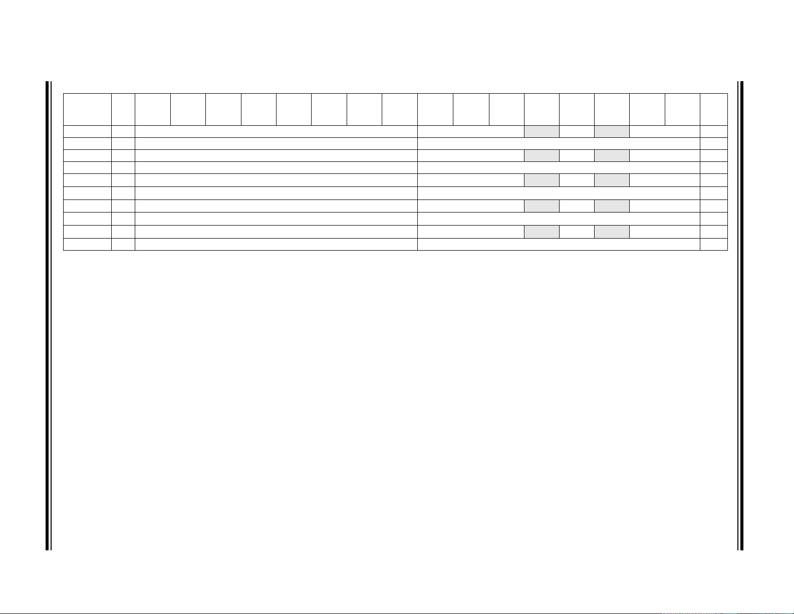
© 2007 Microchip Technology Inc. Preliminary DS70165E-page 63
TABLE 3-23: ECAN2 REGISTER MAP WHEN C2CTRL1.WIN = 1 (CONTINUED)
File Name Addr Bit 15 Bit 14 Bit 13 Bit 12 Bit 11 Bit 10 Bit 9 Bit 8 Bit 7 Bit 6 Bit 5 Bit 4 Bit 3 Bit 2 Bit 1 Bit 0
C2RXF11SID 056C SID<10:3 SID<2:0> — EXIDE — EID<17:16> xxxx
C2RXF11EID 056E EID<15:8> EID<7:0> xxxx
C2RXF12 SID 0570 SID<10:3 SID<2:0>
C2RXF12EID 0572 EID<15:8> EID<7:0> xxxx
C2RXF13SID 0574 SID<10:3
C2RXF13EID 0576 EID<15:8>
C2RXF14SID 0578 SID<10:3
C2RXF14EID 057A EID<15:8>
C2RXF15SID 057C SID<10:3
C2RXF15EID 057E EID<15:8> EID<7:0> xxxx
Legend: x = unknown value on Reset, — = unimplemented, read as ‘0’. Reset values are shown in hexadecimal.
SID<2:0>
SID<2:0>
SID<2:0>
— EXIDE — EID<17:16> xxxx
— EXIDE — EID<17:16>
EID<7:0>
— EXIDE — EID<17:16>
EID<7:0>
— EXIDE — EID<17:16>
Reset
xxxx
xxxx
xxxx
xxxx
xxxx
All
s
dsPIC33F
Page 66

DS70165E-page 64 Preliminary © 2007 Microchip Technology Inc.
dsPIC33F
TABLE 3-24: DCI REGISTER MAP
SFR
Name
DCICON1 0280 DCIEN
DCICON2 0282
DCICON3 0284
DCISTAT 0286
TSCON 0288 TSE15 TSE14 TSE13 TSE12 TSE11 TSE10 TSE9 TSE8 TSE7 TSE6 TSE5 TSE4 TSE3 TSE2 TSE1 TSE0 0000 0000 0000 0000
RSCON 028C RSE15 RSE14 RSE13 RSE12 RSE11 RSE10 RSE9 RSE8 RSE7 RSE6 RSE5 RSE4 RSE3RSE2 RSE1 RSE0 0000 0000 0000 0000
RXBUF0 0290 Receive Buffer #0 Data Register 0000 0000 0000 0000
RXBUF1 0292 Receive Buffer #1 Data Register 0000 0000 0000 0000
RXBUF2 0294 Receive Buffer #2 Data Register 0000 0000 0000 0000
RXBUF3 0296 Receive Buffer #3 Data Register 0000 0000 0000 0000
TXBUF0 0298 Transmit Buffer #0 Data Register 0000 0000 0000 0000
TXBUF1 029A Transmit Buffer #1 Data Register 0000 0000 0000 0000
TXBUF2 029C Transmit Buffer #2 Data Register 0000 0000 0000 0000
TXBUF3 029E Transmit Buffer #3 Data Register 0000 0000 0000 0000
Legend: — = unimplemented, read as ‘0’.
Note 1: Refer to the “dsPIC30F Family Reference Ma nual” (DS70046) for descriptions of register bit fields.
TABLE 3-25: PORTA REGISTER MAP
File Name Addr Bit 15 Bit 14 Bit 13 Bit 12 Bit 11 Bit 10 Bit 9 Bit 8 Bit 7 Bit 6 Bit 5 Bit 4 Bit 3 Bit 2 Bit 1 Bit 0
TRISA 02C0
PORTA 02C2
LATA 02C4
ODCA
Legend: x = unknown value on Reset, — = unimplemented, read as ‘0’. Reset values are shown in hexadecimal for 100-pin devices.
Note 1 : The actual set of I/O port pins varies from one device to another. Please refer to the corresponding pinout diagrams.
Addr. Bit 15 Bit 14 Bit 13 Bit 12 Bit 11 Bit 10 Bit 9 Bit 8 Bit 7 Bit 6 Bit 5 Bit 4 Bit 3 Bit 2 Bit 1 Bit 0 Reset State
— DCISIDL — DLOOP CSCKD CSCKE COFSD UNFM CSDOM DJST — — — COFSM1 COFSM0 0000 0000 0000 0000
— — — — BLEN1 BLEN0 — COFSG<3:0> — WS<3:0> 0000 0000 0000 0000
— — — —BCG<11:0>0000 0000 0000 0000
— — — — SLOT3 SLOT2 SLOT1 SLOT0 — — — — ROV RFUL TUNF TMPTY 0000 0000 0000 0000
(1)
TRISA15 TRISA14 TRISA13 TRISA12 — TRISA10 TRISA9 — TRISA7 TRISA6 TRISA5 TRISA4 TRISA3 TRISA2 TRISA1 TRISA0
RA15 RA14 RA13 RA12 — RA10 RA9 — RA7 RA6 RA5 RA4 RA3 RA2 RA1 RA0
(2)
LATA15 LAT A 14 LATA13 LATA12 — LATA10 LATA9 — LATA7 LATA6 LATA5 LATA4 LATA3 LATA2 LATA1 LATA0
06C0
ODCA15 ODCA14 ODCA13 ODCA12 — — — — — — ODCA5 ODCA4 ODCA3 ODCA2 ODCA1 ODCA0
All
Resets
D6C0
xxxx
xxxx
xxxx
TABLE 3-26: PORTB REGISTER MAP
File Name Addr Bit 15 Bit 14 Bit 13 Bit 12 Bit 11 Bit 10 Bit 9 Bit 8 Bit 7 Bit 6 Bit 5 Bit 4 Bit 3 Bit 2 Bit 1 Bit 0
TRISB 02C6 TRISB15 TRISB14 TRISB13 TRISB12 TRISB11 TRISB10 TRISB9 TRISB8 TRISB7 TRISB6 TRISB5 TRISB4 TRISB3 TRISB2 TRISB1 TRISB0
PORTB 02C8 RB15 RB14 RB13 RB12 RB11 RB10 RB9 RB8 RB7 RB6 RB5 RB4 RB3 RB2 RB1 RB0
LATB 02CA LATB15 LATB14 LATB13 LA TB12 LATB11 LATB10 LATB9 LATB8 LATB7 LATB6 LATB5 LATB4 LA TB3 LA TB 2 LATB1 LA TB0
Legend: x = unknown value on Reset, — = unimplemented, read as ‘0’. Reset values are shown in hexadecimal for 100-pin devices.
Note 1 : The actual set of I/O port pins varies from one device to another. Please refer to the corresponding pinout diagrams.
(1)
All
Resets
FFFF
xxxx
xxxx
Page 67
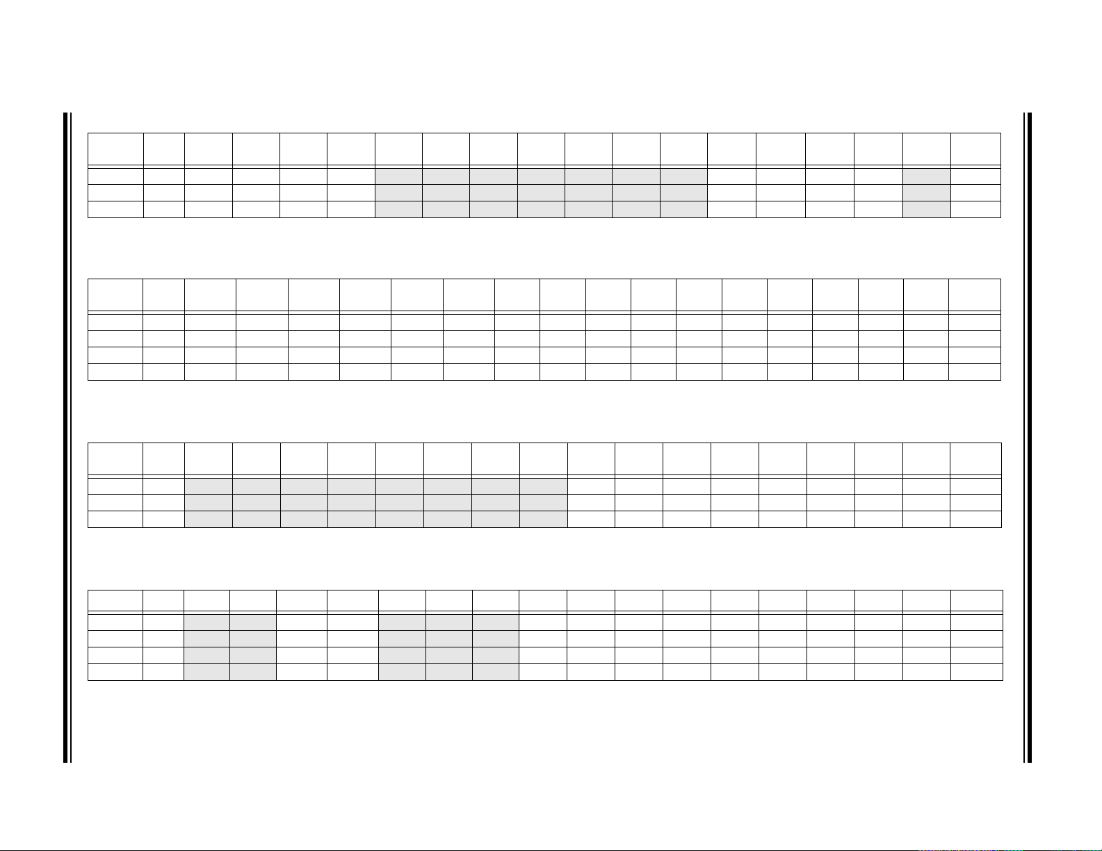
© 2007 Microchip Technology Inc. Preliminary DS70165E-page 65
TABLE 3-27: PORTC REGISTER MAP
File Name Addr Bit 15 Bit 14 Bit 13 Bit 12 Bit 11 Bit 10 Bit 9 Bit 8 Bit 7 Bit 6 Bit 5 Bit 4 Bit 3 Bit 2 Bit 1 Bit 0
TRISC 02CC TRISC15 TRISC14 TRISC13 TRISC12 — — — — — — —
PORTC 02CE RC15 RC14 RC13 RC12 — — — — — — —
LATC 02D0 LATC15 LATC14 LATC13 LATC12 — — — — — — —
Legend: x = unknown value on Reset, — = unimplemented, read as ‘0’. Reset values are shown in hexadecimal for 100-pin devices.
Note 1 : The actual set of I/O port pins varies from one device to another. Please refer to the corresponding pinout diagrams.
(1)
TRISC4 TRISC3 TRISC2 TRISC1 —
RC4 RC3 RC2 RC1 —
LATC 4 LATC 3 LATC 2 LATC 1 —
All
Resets
F01E
xxxx
xxxx
TABLE 3-28: PORTD REGISTER MAP
File Name Addr Bit 15 Bit 14 Bit 13 Bit 12 Bit 11 Bit 10 Bit 9 Bit 8 Bit 7 Bit 6 Bit 5 Bit 4 Bit 3 Bit 2 Bit 1 Bit 0
TRISD 02D2
PORTD 02D4
LAT D 02D6
ODCD 06D2
Legend: x = unknown value on Reset, — = unimplemented, read as ‘0’. Reset values are shown in hexadecimal for 100-pin devices.
Note 1 : The actual set of I/O port pins varies from one device to another. Please refer to the corresponding pinout diagrams.
TRISD15 TRISD14 TRISD13 TRISD12
RD15 RD14 RD13 RD12
LATD15 LATD14 LATD13 LATD12
ODCD15 ODCD14 ODCD13 ODCD12 ODCD11 ODCD10 ODCD9 ODCD8 ODCD7 ODCD6 ODCD5 ODCD4 ODCD3 ODCD2 ODCD1 ODCD0
TABLE 3-29: PORTE REGISTER MAP
File Name Addr Bit 15 Bit 14 Bit 13 Bit 12 Bit 11 Bit 10 Bit 9 Bit 8 Bit 7 Bit 6 Bit 5 Bit 4 Bit 3 Bit 2 Bit 1 Bit 0
TRISE 02D8 — — — — — — — —
PORTE 02DA — — — — — — — —
LAT E 02DC — — — — — — — —
Legend: x = unknown value on Reset, — = unimplemented, read as ‘0’. Reset values are shown in hexadecimal for 100-pin devices.
Note 1 : The actual set of I/O port pins varies from one device to another. Please refer to the corresponding pinout diagrams.
TABLE 3-30: PORT F REGISTER MAP
File Name Addr Bit 15 Bit 14 Bit 13 Bit 12 Bit 11 Bit 10 Bit 9 Bit 8 Bit 7 Bit 6 Bit 5 Bit 4 Bit 3 Bit 2 Bit 1 Bit 0 All Resets
TRISF 02DE — —
PORTF 02E0 — —
LAT F 02E2 — —
ODCF 06DE — —
Legend: x = unknown value on Reset, — = unimplemented, read as ‘0’. Reset values are shown in hexadecimal for 100-pin devices.
Note 1 : The actual set of I/O port pins varies from one device to another. Please refer to the corresponding pinout diagrams.
TRISF13 TRISF12
RF13 RF12
LATF 13 LATF12
ODCF13 ODCF12
(1)
(1)
(1)
TRISD11 TRISD10 TRISD9 TRISD8 TRISD7 TRISD6 TRISD5 TRISD4 TRISD3 TRISD2 TRISD1 TRISD0
RD11 RD10 RD9 RD8 RD7 RD6 RD5 RD4 RD3 RD2 RD1 RD0
LATD 11 LATD10 LA TD 9 LATD8 LATD7 LATD6 LATD5 LATD4 LATD3 LATD2 LATD1 LATD0
TRISE7
LATE 7
— — —
— — — RF8 RF7 RF6 RF5 RF4 RF3 RF2 RF1 RF0
— — — LATF8 LATF7 LATF6 LATF5 LATF4 LATF3 LATF2 LATF1 LATF0
— — —
TRISF8 TRISF7
ODCF8 ODCF7 ODCF6 ODCF5 ODCF4 ODCF3 ODCF2 ODCF1 ODCF0
TRISE6 TRISE5 TRISE4 TRISE3 TRISE2 TRISE1 TRISE0
RE7
RE6 RE5 RE4 RE3 RE2 RE1 RE0
LATE 6 LATE5 LATE4 LATE3 LATE2 LATE1 LATE0
TRISF6 TRISF5 TRISF4 TRISF3 TRISF2 TRISF1 TRISF0
All
Resets
FFFF
xxxx
xxxx
xxxx
All
Resets
03FF
xxxx
xxxx
31FF
xxxx
xxxx
xxxx
dsPIC33F
Page 68
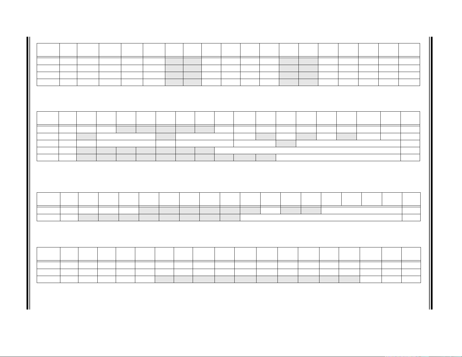
DS70165E-page 66 Preliminary © 2007 Microchip Technology Inc.
TABLE 3-31: PORTG REGISTER MAP
File Name Addr Bit 15 Bit 14 Bit 13 Bit 12 Bit 11 Bit 10 Bit 9 Bit 8 Bit 7 Bit 6 Bit 5 Bit 4 Bit 3 Bit 2 Bit 1 Bit 0
TRISG 02E4
PORTG 02E6
LATG 02E8
ODCG 06E4
Legend: x = unknown value on Reset, — = unimplemented, read as ‘0’. Reset values are shown in hexadecimal for 100-pin devices.
Note 1: The actual set of I/O port pins varies from one device to another. Please refer to the corresponding pinout diagrams.
TRISG15 TRISG14 TRISG13 TRISG12 — — TRISG9 TRISG8 TRISG7 TRISG6 — — TRISG3 TRISG2 TRISG1 TRISG0
RG15 RG14 RG13 RG12 — — RG9 RG8 RG7 RG6 — —RG3RG2RG1RG0
LATG 15 LATG14 LATG13 LATG12 — — LATG9 LATG8 LATG7 LATG6 — —LATG3LATG2LATG1LATG0
ODCG15 ODCG14 ODCG13 ODC G12
(1)
— —
ODCG9 ODCG8 ODCG7 ODCG6 — — ODCG3 ODCG2 ODCG1 ODCG0
All
Resets
F3CF
xxxx
xxxx
xxxx
dsPIC33F
TABLE 3-32: SYSTEM CONTROL REGISTER MAP
File Name Addr Bit 15 Bit 14 Bit 13 Bit 12 Bit 11 Bit 10 Bit 9 Bit 8 Bit 7 Bit 6 Bit 5 Bit 4 Bit 3 Bit 2 Bit 1 Bit 0
RCON 0740 TRAPR IOPUWR — — — — — VREGS EXTR SWR SWDTEN WDTO SLEEP IDLE BOR POR
OSCCON 0742 —COSC<2:0>— NOSC<2:0> CLKLOCK —LOCK—CF— LPOSCEN OSWEN 0300
CLKDIV 0744 ROI DOZE<2:0> DOZEN FRCDIV<2:0> PLLPOST<1:0> — PLLPRE<4::0> 0040
PLLFBD 0746
OSCTUN 0748
Legend: x = unknown value on Reset, — = unimplemented, read as ‘0’. Reset values are shown in hexadecimal.
Note 1 : RCON register Reset values dependent on type of Reset.
2: OSCCON register Reset values dependent on the FOSC Configuration bits and by type of Reset.
— — — — — — — PLLDIV<8:0> 0030
— — — — — — — — — — TUN<5:0> 0000
All
Resets
xxxx
(1)
(2)
TABLE 3-33: NVM REG ISTER MAP
File Name Addr Bit 15 Bit 14 Bit 13 Bit 12 Bit 11 Bit 10 Bit 9 Bit 8 Bit 7 Bit 6 Bit 5 Bit 4 Bit 3 Bit 2 Bit 1 Bit 0
NVMCON 0760 WR WREN WRERR — — — — — — ERASE — —NVMOP<3:0>
NVMKEY 0766
Legend: x = unknown value on Reset, — = unimplemented, read as ‘0’. Reset values are shown in hexadecimal.
Note 1 : Reset value shown is for POR only. Value on other Reset states is dependent on the state of memory write or erase operations at the time of Reset.
— — — — — — — — NVMKEY<7:0>
All
Resets
0000
0000
(1)
TABLE 3-34: PMD RE GISTER MAP
File Name Addr Bit 15 Bit 14 Bit 13 Bit 12 Bit 11 Bit 10 Bit 9 Bit 8 Bit 7 Bit 6 Bit 5 Bit 4 Bit 3 Bit 2 Bit 1 Bit 0
PMD1 0770 T5MD T4MD T3MD T2MD T1MD QEIMD PWMMD DCIMD I2C1MD U2MD U1MD SPI2MD SPI1MD C2MD C1MD AD1MD 0000
PMD2 0772 IC8MD IC7MD IC6MD IC5MD IC4MD IC3MD IC2MD IC1MD OC8MD OC7MD OC6MD OC5MD OC4MD OC3MD OC2MD OC1MD 0000
PMD3 0774 T9MD T8MD T7MD T6MD
Legend: x = unknown value on Reset, — = unimplemented, read as ‘0’. Reset values are shown in hexadecimal.
— — — — — — — — — —I2C2MDAD2MD0000
All
Resets
Page 69
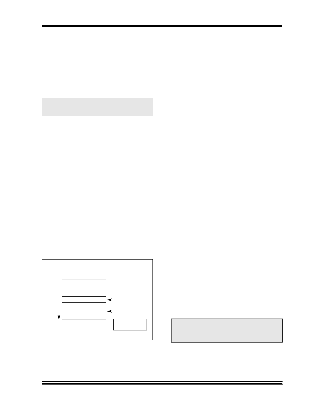
dsPIC33F
3.2.7 SOFTWARE STACK
In addition to its use as a working register, the W15
register in the dsPIC33 F devices is also used as a software Stack Pointer. The S t ac k Point er al wa ys poi nts to
the first available free word and grows from lower to
higher addresses. It pre-decrement s for stack pop s and
post-increments for stack pushes, as shown in
Figure 3-6. For a PC push during any CALL instruction,
the MSb of the PC is zero-extended before the push,
ensuring that the MSb is always clear.
Note: A PC push during exception processing
concatenates the SRL re gis ter to the MSb
of the PC prior to the push.
The Stack Pointer Limit register (SPLIM) associated
with the Stack Pointer sets an upper address boundary
for the stack. SPLIM is uninitialized at Reset. As is the
case for the Stack Pointer, SPLIM<0> is forced to ‘0’
because all stack operations must be word-aligned.
Whenever an EA is generated using W15 as a source
or destination pointer, the resulting address is
compared with the value in SPLIM. If the contents of
the Stack Pointer (W15) and the SPLIM register are
equal and a push operation is performed, a stack error
trap will not occur. The stack error trap will occur on a
subsequent push operation. Thus, for example, if it is
desirable to cause a stac k error trap when the stack
grows beyond address 0x2000 in RAM, initialize the
SPLIM with the value 0x1FFE.
Similarly, a Stack Pointer underflow (sta ck error) tra p is
generated when the Stack Pointer address is found to
be less than 0x0800. This prevents the stack from
interfering with the Special Function Register (SFR)
space.
A write to the SPLIM regis ter should not be immediately
followed by an indirect read operation using W15.
FIGURE 3-6: CALL STACK FRAME
0x0000
Stack Grows Towards
000000000
Higher Address
PC<15:0>
PC<22:16>
<Free Word>
015
W15 (before CALL)
W15 (after CALL)
POP : [--W15]
PUSH : [W15++]
3.2.8 DATA RAM PROTECTION FEATU RE
The dsPIC33F product family supports Data RAM protection features which enable segments of RAM to be
protected when used in conjunction with Boot and
Secure Code Segm ent Secu rity. BSRAM (Secure RAM
segment for BS) is accessible only from the Boot Segment Flash code when ena bled. SSRAM (Sec ure RAM
segment for RAM) is accessible only from the Secure
Segment Flash code when enabled. See Table 3-1 for
an overview of the BSRAM and SSRAM SFRs.
3.3 Instruction Addressing Modes
The address ing mode s in Table 3 -3 5 form the b asis of
the addressing mode s optimized to support the specific
features of individual instructions. The addressing
modes provided in the MAC class of instructions are
somewhat different from those in the other instruction
types.
3.3.1 FILE REGISTER INSTRUCTIONS
Most file register ins truc tio ns use a 13-bit address field
(f) to directly address data present in the first 8192
bytes of data memory (Near Data Space). Most file
register instructions employ a working register, W0,
which is de noted as WREG i n these instruc tions. The
destination is typically either the same file register or
WREG (with the exception of the MUL instruction),
which writes the re sult t o a re gister or regi ster p air. The
MOV instruction allows additional flexibility and can
access the entire data space.
3.3.2 MCU INSTRUCTIONS
The 3-operand MCU instructions are of the form:
Operand 3 = Operand 1 <function> Operand 2
where Operand 1 is alw a ys a work in g reg ist er (i.e., the
addressing mode can only be register direct) which is
referred to as Wb. Operand 2 can be a W register,
fetched from data memory, or a 5-bit literal. The result
location can be either a W register or a data memory
location. The following addressing modes are
supported by MCU instructions:
• Register Direct
• Register Indirect
• Register Indirect Post-Modified
• Register Indirect Pre-Modified
• 5-bit or 10-bit Literal
Note: Not all instructions support all the
addressing modes given above. Individual
instructions may support different subsets
of these addressing modes.
© 2007 Microchip Technology Inc. Preliminary DS70165E-page 67
Page 70
dsPIC33F
TABLE 3-35: FUNDAMENTAL ADDRESSING MODES SUPPORTED
Addressing Mode Description
File Register Direct The address of the file register is specified explicitly.
Register Direct The contents of a register are accessed directly.
Register Indirect The contents of Wn forms the EA.
Register Indirect Post-Modified The contents of Wn forms the EA. Wn is post-modified (incremented or
decremented) by a constant value.
Register Indirect Pre-Modified Wn is pre-modified (incremented or decremented) by a signed constant value
to form the EA.
Register Indirect with Register Offset The sum of Wn and Wb forms the EA.
Register Indirect with Literal Offset The sum of Wn and a literal forms the EA.
3.3.3 MOVE AND ACCUMULATOR INSTRUCTIONS
Move instructions and the DSP accumulator class of
instructions provide a greater degree of addressing
flexibility than other instructions. In addition to the
Addressing modes supported by most MCU instructions, move and accumulator instructions also support
Register Indirect with Register Offset Addressing
mode, also referred to as Register Indexed mode.
Note: For the MOV instructions, the Addressing
mode specified in the instruction can differ
for the source and destination EA.
However, the 4-bit Wb (Register Offset)
field is shared between both source and
destination (but typically only used by
one).
In summary, the following Addressing modes are
supported by move and accumulator instructions:
• Register Direct
• Register Indirect
• Register Indirect Post-modified
• Register Indirect Pre-modif ied
• Register Indirect with Register Offset (Indexed)
• Register Indirect with Literal Offset
• 8-bit Literal
• 16-bit Literal
Note: Not all instructions support all the
Addressing modes gi ven above. Indivi dual
instructions may support different subsets
of these Addressing modes.
3.3.4 MAC INSTRUCTIONS
The dual source operand DSP instructions (CLR, ED,
EDAC, MAC, MPY, MPY.N, MOVSAC and MSC), also referred
to as MAC instructions, utilize a s impl if ie d s et of addressing modes to allow the user to ef fe ctively manipulate the
data pointers t hro ugh register indirect tables .
The 2-source operand prefetch registers must be
members of the set {W8, W9, W10, W11}. For data
reads, W8 and W9 are always directed to the X RAGU
and W10 and W11 will always be directed to the Y
AGU. The effective addresses generated (before and
after modification) must, therefore, be valid addresses
within X data space for W8 and W9 and Y data space
for W10 and W11.
Note: Register Indirect with Register Offset
Addressing mode is only available for W9
(in X space) and W11 (in Y space).
In summary, the following addressing modes are
supported by the MAC class of instructions:
• Register Indirect
• Register Indirect Post-Modified by 2
• Register Indirect Post-Modified by 4
• Register Indirect Post-Modified by 6
• Register Indirect with Register Offset (Indexed)
3.3.5 OTHER INSTRUCTIONS
Besides the var ious addressi ng modes outlin ed above,
some instructio ns use literal constants of vario us sizes.
For example, BRA (branch) in struction s use 16- bit signe d
literals to spe cify the branch dest inatio n directly, whereas
the DISI instruction uses a 14-bit unsigned literal field. In
some instructio ns, such as ADD Acc, the sourc e of an
operand or resu lt is imp li ed by the o pco de itse lf. Cer tain
operations, s uc h as NOP, do not have any operands.
3.4 Modulo Addressing
Modulo Addressing mode is a method of providing an
automated means to support ci rcular dat a buf fers using
hardware. The objectiv e is to remo ve t he need fo r software to perform data address boundary checks when
executing tightly looped code, as is typical in many
DSP algorithms.
Modulo Addressing can operate in either d ata or program
space (since th e data pointer me chanism is essen tially
the same for both). One ci rcul ar buf fer ca n be suppo rte d
in each of the X (which also provides the pointers into
program space) and Y data space s. Mod ulo Ad dr e ssi ng
can operate on an y W reg is te r po in te r. However, it is not
DS70165E-page 68 Preliminary © 2007 Microchip Technology Inc.
Page 71
dsPIC33F
advisable to use W14 or W15 for Modulo Addressing
since these two registers are used as the Stack Frame
Pointer and Stack Pointer, respectively.
In general, any particular circular buffer can only be
configured to operate in one direction as there are
certain restrictio ns on the buf fer start add ress (for incrementing buffers), or end address (for decrementing
buffers), based upon the direction of the buffer.
The only exception to the usage restrictions is for buffers which have a power-of-2 length. As these buffers
satisfy the start and end address criteria, they may
operate in a bidirectiona l mo de (i.e., ad dress boun dary
checks will be performed on both the lower and upper
address boundaries).
3.4.1 START AND END ADDRESS
The Modulo Addressing scheme requires that a starting
and ending address be specified and loaded into the
16-bit Modulo Buffer Address registers: XMODSRT,
XMODEND, YMODSRT and YMODEND (see
Table 3-1).
Note: Y space Modulo Addressing EA calcula-
tions assume word sized data (LSb of
every EA is always clea r) .
The length of a circular buffer is not directly specified. It
is determined by the difference between the corresponding start and end addresses. The maximum possible
length of the circular buffer is 32K words (64 Kbytes).
3.4.2 W ADDRESS REGISTER SELECTION
The Modulo and Bit-Reversed Addressing Control
register, MODCON<15:0>, contains enable flags as well
as a W register f ield t o s pe cify th e W Ad dr es s re gi st ers.
The XWM and YWM fields select which registers will
operate with Modulo Addressing. If XWM = 15, X RAGU
and X WAGU Modulo Addressing is disabled. Similarly, if
YWM = 15, Y AGU Modulo Addressing is disabled.
The X Address Space Pointer W register (XWM), to
which Modulo Addressing is to be applied, is stored in
MODCON<3:0> (see Table 3-1). Modulo Addressing is
enabled for X dat a space when XWM is set to any v alue
other than ‘15’ and the XMODEN bit is set at
MODCON<15>.
The Y Address Space Pointer W register (YWM) to
which Modulo Addressing is to be applied is stored in
MODCON<7:4>. Modulo Addressing is enabled for Y
data space when YWM is set to any value other than
FIGURE 3-7: MODULO ADDRESSING OPERATION EXAMPLE
Byte
Address
0x1100
0x1163
Start Addr = 0x1100
End Addr = 0x1163
Length = 0x0032 words
MOV #0x1100, W0
MOV W0, XMODSRT ;set modulo start address
MOV #0x1163, W0
MOV W0, MODEND ;set modulo end address
MOV #0x8001, W0
MOV W0, MODCON ;enable W1, X AGU for modulo
MOV #0x0000, W0 ;W0 holds buffer fill value
MOV #0x1110, W1 ;point W1 to buffer
DO AGAIN, #0x31 ;fill the 50 buffer locations
MOV W0, [W1++] ;fill the next location
AGAIN: INC W0, W0 ;increment the fill value
© 2007 Microchip Technology Inc. Preliminary DS70165E-page 69
Page 72

dsPIC33F
3.4.3 MODULO ADDRESSING APPLICABILITY
Modulo Addressing can be applied to the Effective
Address (EA) calculation associated with any W
register. It is important to realize that the address
boundaries check for addresses less than, or greater
than, the upper (for inc rementing buf fers) and lower (for
decrementing buffers) boundary addresses (not just
equal to). Address changes may, therefore, jump
beyond boundaries and sti ll be adj us ted co rrec t ly.
Note: The modulo corrected effe cti ve add res s i s
written back to the register only when
Pre-Modify or Post-Modify Addressing
mode is used to compute the effective
address. When an address offset (e.g.,
[W7+W2]) is used, Modulo Address correction is performed but the contents of
the register remain unchanged.
3.5 Bit-Reversed Addressing
Bit-Reversed Addressing mode is intended to simplify
data re-ordering for radix-2 FFT algorithms. It is
supported by the X AGU for data writes only.
The modifier, which may be a constan t val ue or r egist er
content s, is rega rded as having it s bit o rder reve rsed. The
address source and destination are kept in normal order.
Thus, the only operand requiring reversal is the modifier.
3.5.1 BIT-REVERSED ADDRESSING IMPLEMENTATION
Bit-Reversed Addressing mode is enabled when:
1. BWM bits (W register selection) in the
MODCON register are any val ue other than ‘15’
(the stack cannot be accessed using
Bit-Reversed Addressing).
2. The BREN bit is set in the XBREV register.
3. The addressing mode used is Register Indirect
with Pre-Increment or Post-Increment.
N
If the length of a bit- reversed buffer is M = 2
the last ‘N’ bits of the da ta buffer start address must
be zeros.
XB<14:0> is the Bit-Reversed Address modifier, or
‘pivot point’, which is ty pically a const ant. In the ca se of
an FFT computa tion, its v alue is equal to half of the FFT
data buffer size.
Note: All bit-reversed EA calculations assume
word sized data (LSb of every EA is
always clear). The XB value is scaled
accordingly to generate compatible (byte)
addresses.
When enabled, Bit-Reversed Addressing is only executed for Register Indirect with Pre-Increment or
Post-Increment Addre ssing and word siz ed data writes .
It will not function for an y ot her a ddre ss in g mo de o r for
byte sized data and normal addresses are generated
instead. When Bit-Reversed Addressing is active, the
W Address Pointer is always added to the address
modifier (XB) and the of fs et a ssoc iat ed w it h the Regis ter Indirect Addressing mode is ignored. In addition, as
word sized data is a requirement, the LSb of the EA is
ignored (and always clear).
Note: Modulo Addressing and Bit-Reversed
Addressing should not be enabled
together. In the event tha t the user attempts
to do so, Bit-Reversed Addressing will
assume priority when active for the X
WAGU and X WA GU Modulo Addressing
will be disabled. However, Modulo
Addressing will continue to function in the X
RAGU.
If Bit-Reversed Addressing has already been enabled
by setting the BREN (XBREV<15>) bit, then a write to
the XBREV register sho uld not be immedi ately followed
by an indirect read operation using the W register that
has been designated as the bit-reversed pointer.
bytes,
DS70165E-page 70 Preliminary © 2007 Microchip Technology Inc.
Page 73
FIGURE 3-8: BIT-REVERSED ADDRESS EXAMPLE
Sequenti al Address
b15 b14 b13 b12
b7 b6 b5 b4b11 b10 b9 b8
b3 b2 b1 0
dsPIC33F
Bit Locations Swapped Left-to-Right
Around Center of Binary Value
b15 b14 b13 b12
b11 b10 b9 b8
b7 b6 b5 b1
b2 b3 b4
0
Bit-Reversed Address
Pivot Point
XB = 0x0008 for a 16-Word Bit-Reversed Buffer
TABLE 3-36: BIT-REVERSED ADDRESS SEQUENCE (16-ENTRY)
Normal Address Bit-Reversed Address
A3 A2 A1 A0 Decimal A3 A2 A1 A0 Decimal
0000 0 0000 0
0001 1 1000 8
0010 2 0100 4
0011 3 1100 12
0100 4 0010 2
0101 5 1010 10
0110 6 0110 6
0111 7 1110 14
1000 8 0001 1
1001 9 1001 9
1010 10 0101 5
1011 11 1101 13
1100 12 0011 3
1101 13 1011 11
1110 14 0111 7
1111 15 1111 15
© 2007 Microchip Technology Inc. Preliminary DS70165E-page 71
Page 74

dsPIC33F
3.6 Interfacing Program and Data
Memory Spaces
The dsPIC33F architecture uses a 24-bit wid e program
space and a 16-bit wide data sp ace. The arc hitecture is
also a modified Harvard scheme, meaning that data
can also be present in the program space. To use this
data successf ully, it must be accessed in a way that
preserves the alignment of inform ati on in both spaces.
Aside from normal execution, the dsPIC33F architecture provides two methods by which program space
can be accessed during operatio n:
• Using table in stru ctions to acce ss in divid ual by tes
or words anywhere in the program space
• Remapping a portion of the program space into
the data space (Program Space Visibility)
Table instructions allow an application to read or write
to small areas of the program memory. This capability
makes the method ideal for accessing data tables that
need to be updated from time to time. It also allows
access to all bytes of the program word. The remapping method allows an application to access a large
block of data on a read-only basis, which is ideal for
look ups from a large table of static data. It can only
access the least significant word of the program word.
3.6.1 ADDRESSING PROGRAM SPACE
Since the address ranges for the data and program
spaces are 16 and 24 bits, respectively, a method is
needed to create a 23-bit or 24-bit program address
from 16-bit data regist ers. The solution de pends on the
interface method to be used.
For table operations, the 8-bit Table Page register
(TBLPAG) is used to define a 32K word region within
the program space. This is concatenated with a 16-bit
EA to arrive at a full 24-bit program space address. In
this format, the Most Significant bit of TBLPAG is used
to determine if the ope ration occurs in the user memory
(TBLPAG<7> = 0) or the configuration memory
(TBLPAG<7> = 1).
For remapping operations, the 8-bit Program Space
Visibility register (PSVPAG) is used to define a
16K word page in the program space. When the Most
Significant bit of th e EA is ‘1’, PSVPAG is concaten ated
with the lower 15 b its of t he EA to form a 23-bit program
space address. Unlike table operations, this limits
remapping operati ons stric tly to the u ser m emory area.
T abl e 3-37 and Figure 3-9 show how the prog ram EA is
created for table operations and remapping accesses
from the data EA. Here, P<23:0> refers to a program
space word, whereas D<15:0> refers to a data space
word.
TABLE 3-37: PROGRAM SPACE ADDRESS CONSTRUCTION
Access Type
Instruction Access
(Code Execution)
TBLRD/TBLWT
(Byte/Word Read/Write)
Program Space Visibility
(Block Remap/Read)
Note 1: Data EA<15> is always ‘1’ in this case, but is not used in c alculati ng th e progra m sp ace addre ss. Bit 15 of
the address is PSVPAG<0>.
Access
Space
User 0 PC<22:1> 0
User TBLPAG<7:0> Data EA<15:0>
Configuration TBLPAG<7:0> Data EA<15:0>
User 0 PSVPAG<7:0> Data EA<14:0>
<23> <22:16> <15> <14:1> <0>
0xx xxxx xxxx xxxx xxxx xxx0
0xxx xxxx xxxx xxxx xxxx xxxx
1xxx xxxx xxxx xxxx xxxx xxxx
0 xxxx xxxx xxx xxxx xxxx xxxx
Program Space Address
(1)
DS70165E-page 72 Preliminary © 2007 Microchip Technology Inc.
Page 75

dsPIC33F
FIGURE 3-9: DATA ACCESS FROM PROGRAM SPACE ADDRESS GENERATION
Program Counter
Table Operations
Program Space Visibility
(Remapping)
(1)
(2)
User/Configuration
0
1/0
(1)
0
Space Select
TBLPAG
8 bits
Select
PSVPAG
8 bits
23 bits
24 bits
1
23 bits
EA
16 bits
EA
15 bits
0Program Counter
1/0
0
Byte Select
Note 1: The LSb of program spac e addresses is always fixed as ‘0’ in order to ma intain word
alignment of data in the program and data spaces.
2: Table operations are not require d t o b e w o rd-al ign ed . Table read ope rati on s a r e p erm itt ed
in the configuration memory space.
© 2007 Microchip Technology Inc. Preliminary DS70165E-page 73
Page 76

dsPIC33F
3.6.2 DATA ACCESS FROM PROGRAM MEMORY USING TABLE INSTRUCTIONS
The TBLRDL and TBLWTL instructions offer a direct
method of reading or writing the lower word of any
address within the program space without going
through data sp ac e. The TBLRDH and TBLWTH instruc-
tions are the only method to read or write the upper
8 bits of a program space word as data.
The PC is incremented by two for each successive
24-bit program word. This allows program memory
addresses to directly map to data space addresses.
Program memory can thus be regarded as two 16-bit
word wide address sp ac es , res id ing si de by si de, each
with the same address range. TBLRDL and TBLWTL
access the space which contains the least significant
data word and TBLRDH and TBLWTH access the space
which contains the upper data byte.
Two table instructions are provided to move byte or
word sized (16-bit) data to and from program space.
Both function as either byte or word operations.
1. TBLRDL (Table Read Low): In Word mode, it
maps the lower word of the program space
location (P<15:0>) to a data add ress (D<1 5:0>).
In Byte mode, either the upper or lower byte of
the lower program word is mapped to the lower
byte of a data address. The upper byte is
selected when Byte Select is ‘1’; the lower byte
is selected when it is ‘0’.
2. TBLRDH (Table Read High) : In Word mode, it
maps the entire upper word of a program address
(P<23:16>) to a data address. Note that
D<15:8>, the ‘phantom byte’, will always be ‘0’.
In Byte mode, it map s the up per or lo wer byte of
the program word to D<7:0> of the data
address, as above. Note that the data will
always be ‘0’ when the upper ‘phantom’ byte is
selected (Byte Select = 1).
In a similar fashion, two table instructions, TBLWTH
and TBLWTL, are used to write individual bytes or
words to a program space address. The details of
their operati on are explained in Section 4.0 “Flash
Program Memory”.
For all table operations, the area of program memory
space to be access ed is de termin ed by the Table Page
register (TBLPAG). TBLPAG covers the entire program
memory space of t he device, in cluding use r and confi guration spaces. W hen TBL PAG<7> = 0, the table page
is located in the user memory space. When
TBLPAG<7> = 1, the page is located in configuration
space.
FIGURE 3-10: ACCESSING PROGRAM MEMORY WITH TABLE INSTRUCTIONS
TBLPAG
02
23 15 0
0x000000
0x020000
0x030000
0x800000
Program Space
00000000
00000000
00000000
00000000
‘Phantom’ By te
TBLRDH.B (Wn<0> = 0)
TBLRDL.B (Wn<0> = 1)
TBLRDL.B (Wn<0> = 0)
TBLRDL.W
The address for the table operation is determined by the data EA
within the page defined by the TBLPAG register.
Only read operations are shown; write operations are also valid in
the user memory area.
081623
DS70165E-page 74 Preliminary © 2007 Microchip Technology Inc.
Page 77

dsPIC33F
3.6.3 READING DATA FROM PROGRAM MEMORY USING PROGRAM SPACE VISIBILITY
The upper 32 Kbytes of data space may optionally be
mapped into any 1 6K word page of the pr ogram sp ace.
This option provides tran sparent access of stored constant data from the data space without the need to use
special instructions (i.e., TBLRDL/H).
Program space access through the data space occurs
if the Most Significan t bit of the dat a space EA i s ‘1’ and
program spac e visibil ity is enabl ed by se tting t he PSV
bit in the Core Control register (CORCON<2>). The
location of th e program memory spac e to be mapped
into the data space is determined by the Program
Space Visibility Page register (PSVPAG). This 8-bit
register defines any one of 256 possible pages of
16K words in program space. In effect, PSVPAG functions as the upper 8 bits of the program memory
address, with the 15 bits of the EA functioning as the
lower bits. Note that by incrementing the PC by 2 for
each program memory word, the lower 15 bits of data
space addresses dire ctly map to the lower 15 bit s in the
corresponding program space addresses.
Data reads to this area add an additional cycle to the
instruction being exec uted, sinc e two program me mory
fetches are required.
Although each data space address, 8000h and higher,
maps directly into a corresponding program memory
address (see Figure 3-11), only the lowe r 16 bits of the
24-bit program word are used to contain the data. The
upper 8 bits of any program space location used as
data should be programmed with ‘1111 1111’ or
‘0000 0000’ to force a NOP. This prevents possible
issues should the area of code ever be accidentally
executed.
Note: PSV access is temporarily disabled durin g
table reads/writes.
For operations that use PSV and are executed outside
a REPEAT loop, the MOV and MOV.D instructions
require one instructio n cycle in additi on to the sp ecified
execution time. All other instructions require two
instruction cycles in addition to the specified execution
time.
For operations that use PSV, which are executed ins ide
a REPEAT loop, there will be some instances that
require two instruction cycles in addition to the
specified execution time of the instruction:
• Execution in the first iteration
• Execution in the last iteration
• Execution prior to exiting the loop due to an
interrupt
• Execution upon re-entering the loop after an
interrupt is serviced
Any other iteration of the REPEAT loop will allow the
instruction accessing data, using PSV, to execute in a
single cycle.
FIGURE 3-11: PROGRAM SPACE VISIBILITY OPERATION
When CORCON<2> = 1 and EA<15> = 1:
Program Space
PSVPAG
02
The data in the page
designated by
PSVPAG is mapped
into the upper half of
the data memory
space...
23 15 0
0x000000
0x010000
0x018000
0x800000
Data Space
PSV Area
0x0000
0x8000
0xFFFF
Data EA<14:0>
...while the lower 15 bits
of the EA specify an
exact address within
the PSV area. This
corresponds exactly to
the same lower 15 bits
of the actual program
space address.
© 2007 Microchip Technology Inc. Preliminary DS70165E-page 75
Page 78

dsPIC33F
NOTES:
DS70165E-page 76 Preliminary © 2007 Microchip Technology Inc.
Page 79

dsPIC33F
4.0 FLASH PROGRAM MEMORY
Note: This data sheet summarizes the features
of this group of dsPIC33F devices. It is not
intended to be a compr ehensive refer ence
source. To complement the information in
this data sheet, refer to the “dsPIC30F
Family Reference Manual” (DS70046).
The dsPIC33F devices contain internal Flash program
memory for storing and executing application code.
The memory is readable, writable and erasable during
normal operation over the entire V
Flash memory can be programmed in two ways:
1. In-Circuit Serial Programming™ (ICSP™)
programming capability
2. Run-Time Self-Programming (RTSP)
ICSP allows a dsPIC33F device to be serially
programmed while in t he en d app licati on c ircuit. This is
simply done with two lines for programming clock and
programming data (one of the alt ernate pro gramming
pin pairs: PGC1/PGD1, PGC2/ PGD2 or PGC3/PGD3),
and three other lines fo r power (V
Master Clear (MCLR
). This allows customers to manufacture boards with unprogrammed devices and then
program the digit al signal con troller just befo re shipping
the product. This also allows the most recent firmware
or a custom firmware to be programmed.
DD range.
DD), ground (VSS) and
RTSP is accomplished using TBLRD (table read) and
TBLWT (table write) instructions. With RTSP, the user
can write program memory data either in blocks or
‘rows’ of 64 instructions (192 bytes) at a time or a singl e
program memory word, and erase program memory in
blocks or ‘pages’ of 512 instructions (1536 bytes) at a
time.
4.1 Table Instructions and Flash
Programming
Regardless of the method used, all programming of
Flash memory is done with the table read and table
write instructions. These allow direct read and write
access to the program memory space from the data
memory while the device is in normal operating mode.
The 24-bit target address in the program memory is
formed using bit s<7:0> of the TB LPAG register and the
Effective Address (EA) from a W register specified in
the table instruction, as shown in Figure 4-1.
The TBLRDL and the TBLWTL instructions are used to
read or write to bits<15:0> of program memory.
TBLRDL and TBLWTL can access program memory in
both Word and Byte modes.
The TBLRDH and TBLWTH i nstructio ns are used to read
or write to bits<23:16> of program memory. TBLRDH
and TBLWTH can also access prog ram memory in Word
or Byte mode.
FIGURE 4-1: ADDRESSING FOR TABLE REGISTERS
24 bits
Using
Program Counter
Using
Table Instruction
User/Configuration
Space Select
0
1/0
TBLPAG Reg
8 bits
Program Counter
Working Reg EA
24-bit EA
0
16 bits
Byte
Select
© 2007 Microchip Technology Inc. Preliminary DS70165E-page 77
Page 80

dsPIC33F
4.2 RTSP Operation
The dsPIC33F Flash program memory array is
organized into rows of 64 instructions or 192 bytes.
RTSP allows the user to erase a page of memory,
which consists of eight rows (512 instructions) at a
time, and to program one row or one word at a time.
Table 26- 11, DC Chara cteristics: Program Memor y
shows typical erase and programming times. The 8row erase pages and single row write rows are edgealigned, from the beginning of program memory, on
boundaries of 1536 bytes and 192 bytes, respectively.
The program memory implements holding buffers that
can contain 64 instructions of programming data. Prior
to the actual programming operation, the write data
must be loaded i nto the buffe rs in s equential order. The
instruction words loaded must always be from a group
of 64 boundary.
The basic sequence f or RTSP program ming is to set up
a Table Pointer, then do a series of TBLWT instructions
to load th e buffer s. P rogram ming i s per for med by setting the control bits in the NVMCON register. A total of
64 TBLWTL and TBLWTH i nstruc tions are requ ired t o
load the instructions.
All of the table write operations are single-word writes
(two instruction cycles) because only the buffers are
written. A programming cycle is required for
programming each row.
4.3 Control Registers
There are two SFRs used to read and write the
program Flash memory: NVMCON and NVMKEY.
The NVMCON register (Register 4-1) controls which
blocks are to be erased, which memory type is to be
programmed and the start of the programming cycle.
NVMKEY is a write-only register that is used for write
protection. To start a programming or erase sequence,
the user must consecutively write 55h and AAh to the
NVMKEY register. Refer to Section 4.4 “Programming
Operations” for further details.
4.4 Programming Operations
A complete programming sequence is necessary for
programming or erasing the internal Flash in RTSP
mode. A programming operation is nominally 4 ms in
duration and the processor stalls (waits) until the operation is finished. Setting the WR bit (NVMCON<15>)
starts the operation, and the WR bit is automatically
cleared when the operation is finished.
DS70165E-page 78 Preliminary © 2007 Microchip Technology Inc.
Page 81

dsPIC33F
REGISTER 4-1: NVMCON: FLASH MEMORY CONTROL REGISTER
(1)
R/SO-0
WR WREN WRERR — — — — —
bit 15 bit 8
R/W-0
(1)
R/W-0
(1)
U-0 U-0 U-0 U-0 U-0
U-0 R/W-0
(1)
U-0 U-0 R/W-0
— ERASE — —NVMOP<3:0>
(1)
R/W-0
(1)
R/W-0
(2)
(1)
R/W-0
(1)
bit 7 bit 0
Legend: SO = Satiable only bit
R = Readable bit W = Writable bit U = Unimplemented bit, read as ‘0’
-n = Value at POR ‘1’ = Bit is set ‘0’ = Bit is cleared x = Bit is unknown
bit 15 WR: Write Control bit
1 = Initiates a Flash memory program or erase operation. The operation is self-timed and the bit is
cleared by hardware once operation is complete.
0 = Program or erase operation is complete and inactive
bit 14 WREN: Write Enable bit
1 = Enable Flash program/erase operation s
0 = Inhibit Flash program/erase operations
bit 13 WRERR: Write Sequence Error Flag bit
1 = An improper program or erase sequence attempt or termination has occurred (bit is set
automatically on any set attempt of the WR bit)
0 = The program or erase operation completed normally
bit 12-7 Unimplemented: Read as ‘0’
bit 6 ERASE: Erase/Program Enable bit
1 = Perform the erase operation specified by NVMOP<3:0> on the next WR command
0 = Perform the program operation specified by NVMOP<3:0> on the next WR command
bit 5-4 Unimplemented: Read as ‘0’
(2)
bit 3-0 NVMOP<3:0>: NVM Operation Select bits
1111 = Memory bulk erase operation (ERASE = 1) or no operation (ERASE = 0)
1110 = Reserved
1101 = Erase General Segment and FGS Configuration register
(ERASE = 1) or no operation (ERASE = 0)
1100 = Erase Secure Segment and FSS Configuration register
(ERASE = 1) or no operation (ERASE = 0)
1011 = Reserved
0011 = Memory word program operation (ERASE = 0) or no operation (ERASE = 1)
0010 = Memory page erase operation (ERASE = 1) or no operation (ERASE = 0)
0001 = Memory row program operation (ERASE = 0) or no operation (ERASE = 1)
0000 = Program or erase a singl e Configuration register byte
Note 1: These bits can only be reset on POR.
2: All other combinations of NVMOP<3:0> are unimplemented.
© 2007 Microchip Technology Inc. Preliminary DS70165E-page 79
Page 82

dsPIC33F
4.4.1 PROGRAMMING ALGORITHM FOR FLASH PROGRAM MEMORY
The user can program one row of program Flash
memory at a time. To do this, it is necessary to erase
the 8-row erase page that contains the desired row.
The general process is:
1. Read eight rows of program memory
(512 instructions) and store in data RAM.
2. Update the program data in RAM with the
desired new data.
3. Erase the block (see Example 4-1):
a) Set the NVMOP bits (NVMCON<3:0>) to
‘0010’ to configure for block erase. Set the
ERASE (NVMCON<6>) and WREN (NVMCON<14>) bits.
b) Write the starting address of the page to be
erased into the TBLPAG and W registers.
c) Write 55h to NVMKEY.
d) Write AAh to NVMKEY.
e) Set the WR bit (NVMCON<15>). The erase
cycle begins and the CPU s t al l s fo r t he d u r a-
tion of the erase cycle. When the erase is
done, the WR bit is cleared automatically.
4. Write the first 64 instructions from data RAM into
the program memory b uffers (see Example 4-2).
5. Write the program block to Flash memory:
a) Set the NVMOP bits to ‘0001’ to configure
for row programming. Clear the ERASE bit
and set the WREN bit.
b) Write 55h to NVMKEY.
c) Write AAh to NVMKEY.
d) Set the WR bit. The programming cycle
begins and th e CPU stalls for the duration of
the write cycl e. When the w rite to Flash m em-
ory is done, the WR bit is cleared
automatically.
6. Repeat steps 4 and 5, using the next available
64 instructi ons from the block in data R AM by
incrementing the value in TBLPAG, until all
512 instructions are written back to Flash memory.
For protection against accidental operations, the write
initiate sequence for NVMKEY must be used to allow
any erase or program operation to proceed. After the
programming command has been executed, the user
must wait for t he pro g ram mi ng ti me unt il pro g r am ming
is complete. The two instructions following the start of
the programming se que nce s hould be NOPs, as shown
in Example 4-3.
EXAMPLE 4-1: ERASING A PROGRAM MEMORY PAGE
; Set up NVMCON for block erase operation
MOV #0x4042, W0 ;
MOV W0, NVMCON ; Initialize NVMCON
; Init pointer to row to be ERASED
MOV #tblpage(PROG_ADDR), W0 ;
MOV W0, TBLPAG ; Initialize PM Page Boundary SFR
MOV #tbloffset(PROG_ADDR), W0 ; Initialize in-page EA[15:0] pointer
TBLWTL W0, [W0] ; Set base address of erase block
DISI #5 ; Block all interrupts with priority <7
; for next 5 instructions
MOV #0x55, W0
MOV W0, NVMKEY ; Write the 55 key
MOV #0xAA, W1 ;
MOV W1, NVMKEY ; Write the AA key
BSET NVMCON, #WR ; Start the erase sequence
NOP ; Insert two NOPs after the erase
NOP ; command is asserted
DS70165E-page 80 Preliminary © 2007 Microchip Technology Inc.
Page 83

EXAMPLE 4-2: LOADING THE WRITE BUFFERS
; Set up NVMCON for row programming operations
; Set up a pointer to the first program memory location to be written
; program memory selected, and writes enabled
; Perform the TBLWT instructions to write the latches
; 0th_program_word
; 1st_program_word
; 2nd_program_word
; 63rd_program_word
MOV #0x4001, W0 ;
MOV W0, NVMCON ; Initialize NVMCON
MOV #0x0000, W0 ;
MOV W0, TBLPAG ; Initialize PM Page Boundary SFR
MOV #0x6000, W0 ; An example program memory address
MOV #LOW_WORD_0, W2 ;
MOV #HIGH_BYTE_0, W3 ;
TBLWTL W2, [W0] ; Write PM low word into program latch
TBLWTH W3, [W0++] ; Write PM high byte into program latch
MOV #LOW_WORD_1, W2 ;
MOV #HIGH_BYTE_1, W3 ;
TBLWTL W2, [W0] ; Write PM low word into program latch
TBLWTH W3, [W0++] ; Write PM high byte into program latch
MOV #LOW_WORD_2, W2 ;
MOV #HIGH_BYTE_2, W3 ;
TBLWTL W2,
TBLWTH W3,
•
•
•
MOV #LOW_WORD_31, W2 ;
MOV #HIGH_BYTE_31, W3 ;
TBLWTL W2,
TBLWTH W3,
[W0] ; Write PM low word into program latch
[W0++] ; Write PM high byte into program latch
[W0] ; Write PM low word into program latch
[W0++] ; Write PM high byte into program latch
dsPIC33F
EXAMPLE 4-3: INITIATING A PROGRAMMING SEQUENCE
DISI #5 ; Block all interrupts with priority <7
MOV #0x55, W0
MOV W0, NVMKEY ; Write the 55 key
MOV #0xAA, W1 ;
MOV W1, NVMKEY ; Write the AA key
BSET NVMCON, #WR ; Start the erase sequence
NOP ; Insert two NOPs after the
NOP ; erase command is asserted
; for next 5 instructions
© 2007 Microchip Technology Inc. Preliminary DS70165E-page 81
Page 84

dsPIC33F
NOTES:
DS70165E-page 82 Preliminary © 2007 Microchip Technology Inc.
Page 85
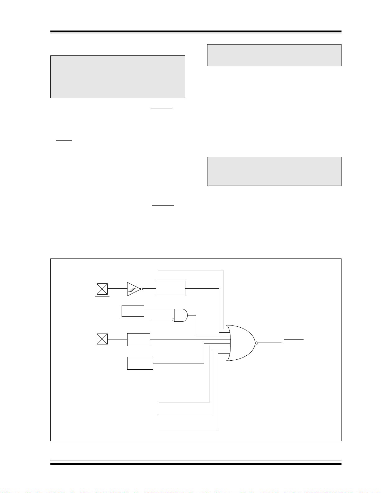
dsPIC33F
5.0 RESETS
Note: This data sheet summarizes the features
of this group of dsPIC33F devices. It is not
intended to be a compr ehensive refer ence
source. To complement the information in
this data sheet, refer to the “dsPIC30F
Family Reference Manual” (DS70046).
The Reset module combines all Reset sources and
controls the device Master Reset Signa l, SYSRST
following is a list of device Reset sources:
• POR: Power-on Reset
• BOR: Brown-out Reset
•MCLR
: Master Clear Pin Reset
•SWR: RESET Instruction
• WDT: Watchdog Timer Reset
• TRAPR: Trap Conflict Reset
• IOPUWR: Illegal Opcode and Uninitialized W
Register Reset
A simplified block diagram of the Reset module is
shown in Figure 5-1.
Any active source of Reset will make the SYSRST si gnal active. Many reg isters asso ciated wit h the CPU and
peripherals are forced to a known Reset state. Most
registers are unaffected by a Reset; their status is
unknown on POR and unchange d by all other Res ets.
. The
Note: Refer to the specific peripheral or CPU
section of this manual for register Reset
states.
All types of device Res et will set a corresp onding statu s
bit in the RCON register to indicate the type of Reset
(see Register 5-1). A POR will clear all bits, except for
the POR bit (RCO N<0>), th at are set. The u ser c an set
or clear any bit at any time during code execution. The
RCON bits only ser ve as status bit s. Setting a particul ar
Reset status bit in software does not cause a device
Reset to occur.
The RCON register also has other bits associated with
the Watchdog Timer and device power-saving states.
The function of these bit s is discusse d in other section s
of this manual.
Note: The status bits in the RCON register
should be cleared after they are read so
that the next RCON register value after a
device Reset will be meaningful.
FIGURE 5-1: RESET SYSTEM BLOCK DIAGRAM
RESET Instruction
Glitch Filter
MCLR
WDT
Module
Sleep or Idle
VDD Rise
VDD
Uninitialized W Register
Detect
Internal
Regulator
Trap Conflict
Illegal Opcode
POR
BOR
SYSRST
© 2007 Microchip Technology Inc. Preliminary DS70165E-page 83
Page 86
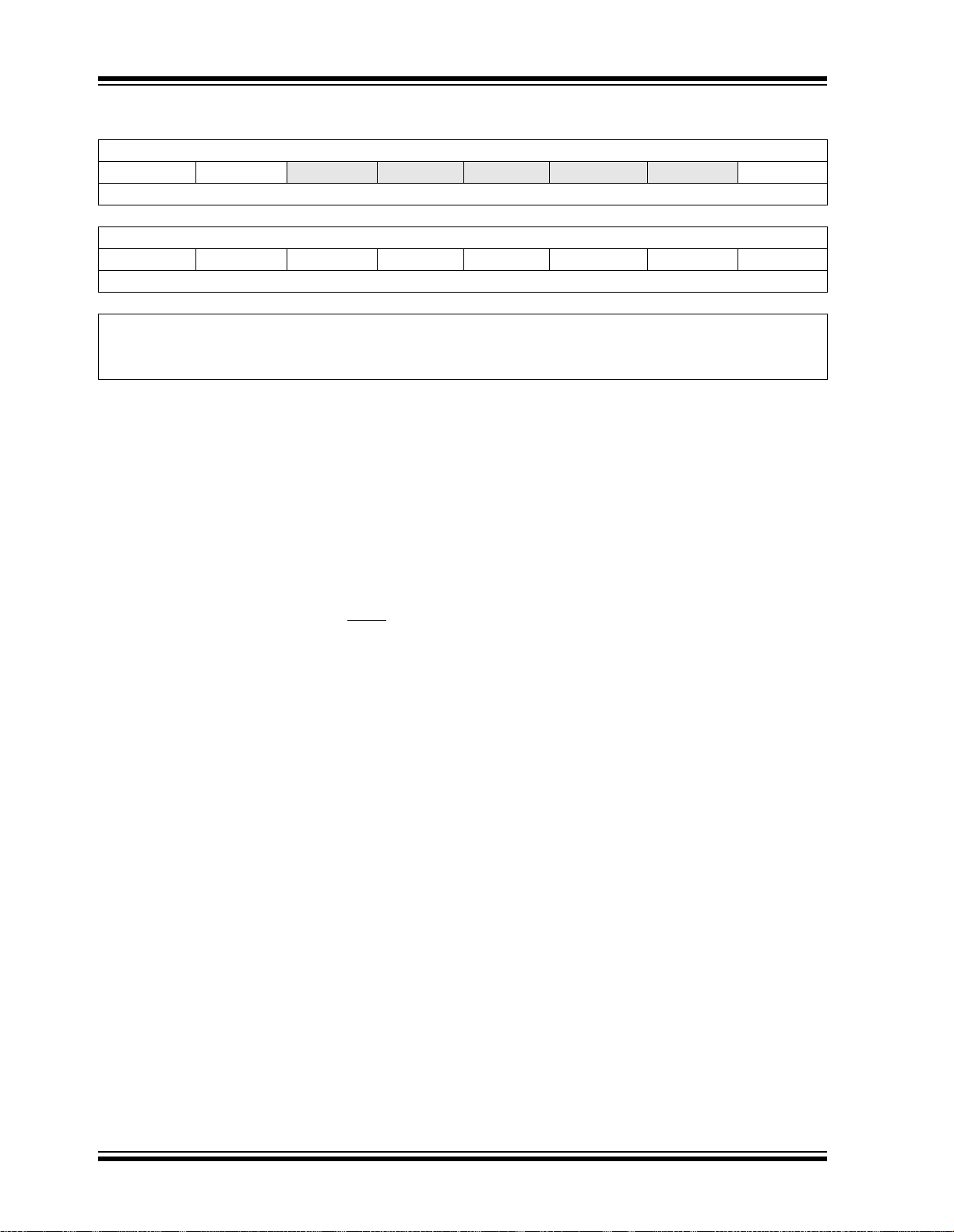
dsPIC33F
REGISTER 5-1: RCON: RESET CONTROL REGISTER
R/W-0 R/W-0 U-0 U-0 U-0 U-0 U-0 R/W-0
TRAPR IOPUWR
bit 15 bit 8
R/W-0 R/W-0 R/W-0 R/W-0 R/W-0 R/W-0 R/W-1 R/W-1
EXTR SWR SWDTEN
bit 7 bit 0
Legend:
R = Readable bit W = Writable bit U = Unimplemented bit, read as ‘0’
-n = Value at POR ‘1’ = Bit is set ‘0’ = Bit is cleared x = Bit is unknown
bit 15 TRAPR: Trap Reset Flag bit
1 = A Trap Conflict Reset has occurred
0 = A Trap Conflict Reset has not occurred
bit 14 IOPUWR: Illegal Opcode or Uninitialized W A ccess Reset F lag bit
1 = An illegal opcode detection, an illegal address mode or uninitialized W register used as an
Address Pointer caused a Reset
0 = An illegal opcode or uninitialized W Reset has not occurred
bit 13-9 Unimplemented: Read as ‘0’
bit 8 VREGS: Voltage Regulator Standby D uring Sleep bit
1 = Voltage regulator goes into Standby mode during Sleep
0 = Voltage regulator is active during Sleep
bit 7 EXTR: External Reset (MCLR
1 = A Master Clear (pin) Reset has occurred
0 = A Master Clear (pin) Reset has not occurred
bit 6 SWR: Software Reset (Instruction) Flag bit
1 = A RESET instruction has been executed
0 = A RESET instruction has not been executed
bit 5 SWDTEN: Software Enable/Disable of WDT bit
1 = WDT is enabled
0 = WDT is disabled
bit 4 WDTO: Watchdog Timer Time-out Flag bit
1 = WDT time-out has occurred
0 = WDT time-out has not occurred
bit 3 SLEEP: Wake-up from Sleep Flag bit
1 = Device has been in Sleep mode
0 = Device has not been in Sleep mode
bit 2 IDLE: Wake-up from Idle Flag bit
1 = Device was in Idle mode
0 = Device was not in Idle mode
bit 1 BOR: Brown-out Reset Flag bit
1 = A Brown-out Reset has occurred
0 = A Brown-out Reset has not occurred
— — — — —VREGS
(2)
WDTO SLEEP IDLE BOR POR
) Pin bit
(1)
(2)
Note 1: All of the Reset status bits may be set or cleared in so ftware. Setting one of these bit s in software does not
cause a device Reset.
2: If the FWDTEN Configuration bit is ‘1’ (unprogrammed), the WDT is always enabled, regardless of the
SWDTEN bit setting.
DS70165E-page 84 Preliminary © 2007 Microchip Technology Inc.
Page 87
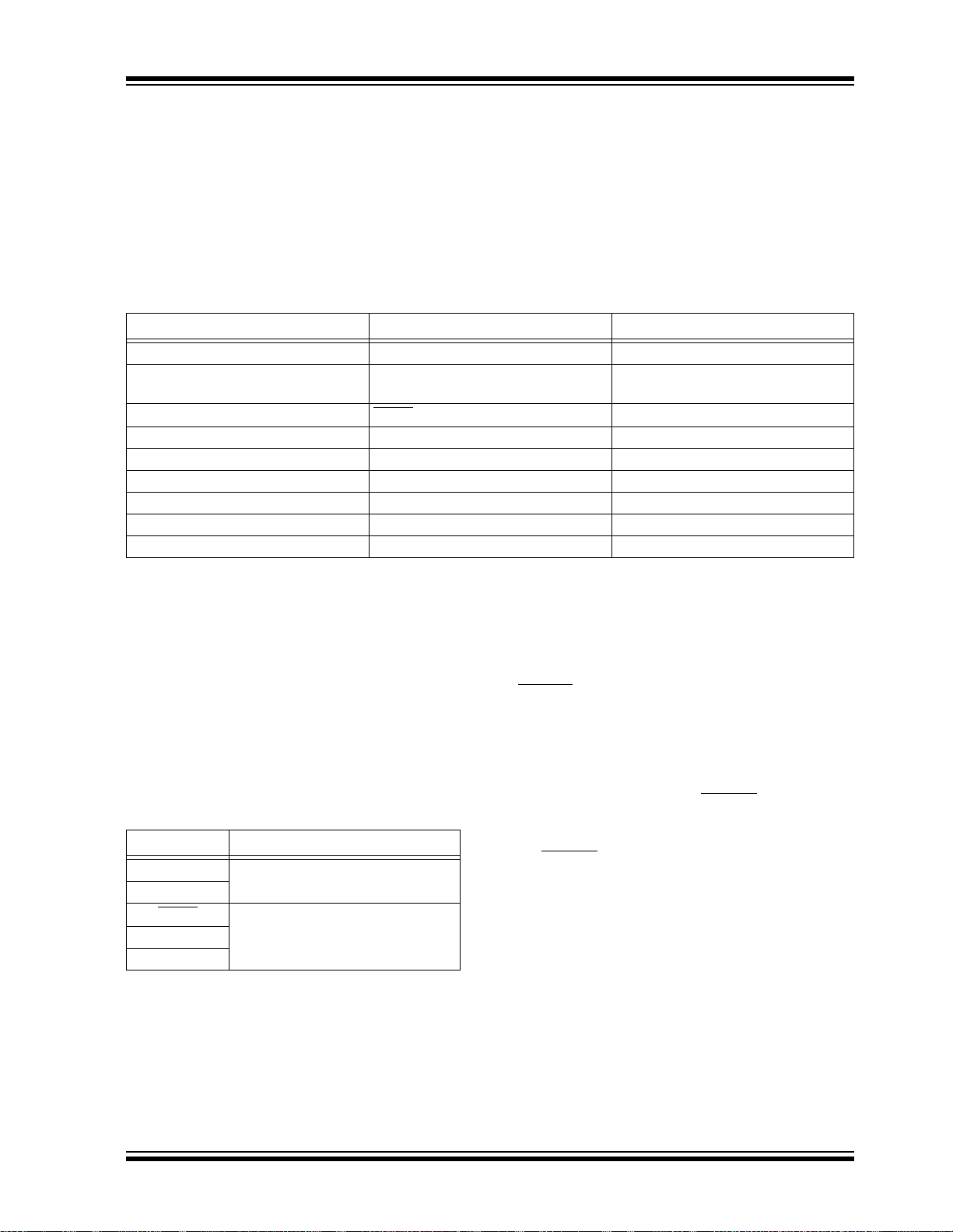
dsPIC33F
REGISTER 5-1: RCON: RESET CONTROL REGISTER
bit 0 POR: Power-on Reset Flag bit
1 = A Power-up Reset has occurred
0 = A Power-up Reset has not occurred
Note 1: All of the Reset status bits may be set or cleared in sof tware. Setting one of these bit s in software does not
cause a device Reset.
2: If the FWDTEN Configuration bit is ‘1’ (unprogrammed), the WDT is always enabled, regardless of the
SWDTEN bit setting.
(1)
TABLE 5-1: RESET FLAG BIT OPERATION
Flag Bit Setting Event Clearing Event
TRAPR (RCON<15>) Trap conflict event POR
IOPUWR (RCON<14>) Illegal opcode or uninitialized
W register access
EXTR (RCON<7>) MCLR
SWR (RCON<6>) RESET instruction POR
WDTO (RCON<4>) WDT time-out PWRSAV instruction, POR
SLEEP (RCON<3>) PWRSAV #SLEEP instruction POR
IDLE (RCON<2>) PWRSAV #IDLE instruction POR
BOR (RCON<1> BOR —
POR (RCON<0>) POR —
Note: All Reset flag bits may be set or cleared by the user software.
Reset POR
POR
5.1 Clock Source Selection at Reset
If clock switching is enabled, the system clock source at
device Reset is chosen, as shown in Table 5-2. If clock
switching is disabled, the s ystem c lock sou rc e i s always
selected according to the oscillator Configuration bits.
Refer to Section 8.0 “Oscillator Configuration” for
further details.
T ABLE 5-2: OSCILLATOR SELECTION vs.
TYPE OF RESET (CLOCK
SWITCHING ENABLED)
Reset Type Clock Source Determinant
POR Oscillator Configuration bits
BOR
MCLR
WDTR
SWR
(FNOSC<2:0>)
COSC Control bits
(OSCCON<14:12>)
5.2 Device Reset Times
The Reset times for various types of device Reset are
summarized in Table 5-3. The system Reset signal,
SYSRST
times expi re.
The time at which the de vice actuall y begins to execu te
code also depends on the system oscillator delays,
which include the Oscillator Start-up Timer (OST) and
the PLL lock time. The OST and PLL lock times occur
in parallel with the applicable SYSRST
The FSCM delay determines the time at which the
FSCM begins to monitor the system clock source after
the SYSRST
, is released after the POR and PWRT delay
delay times.
signal is released.
© 2007 Microchip Technology Inc. Preliminary DS70165E-page 85
Page 88
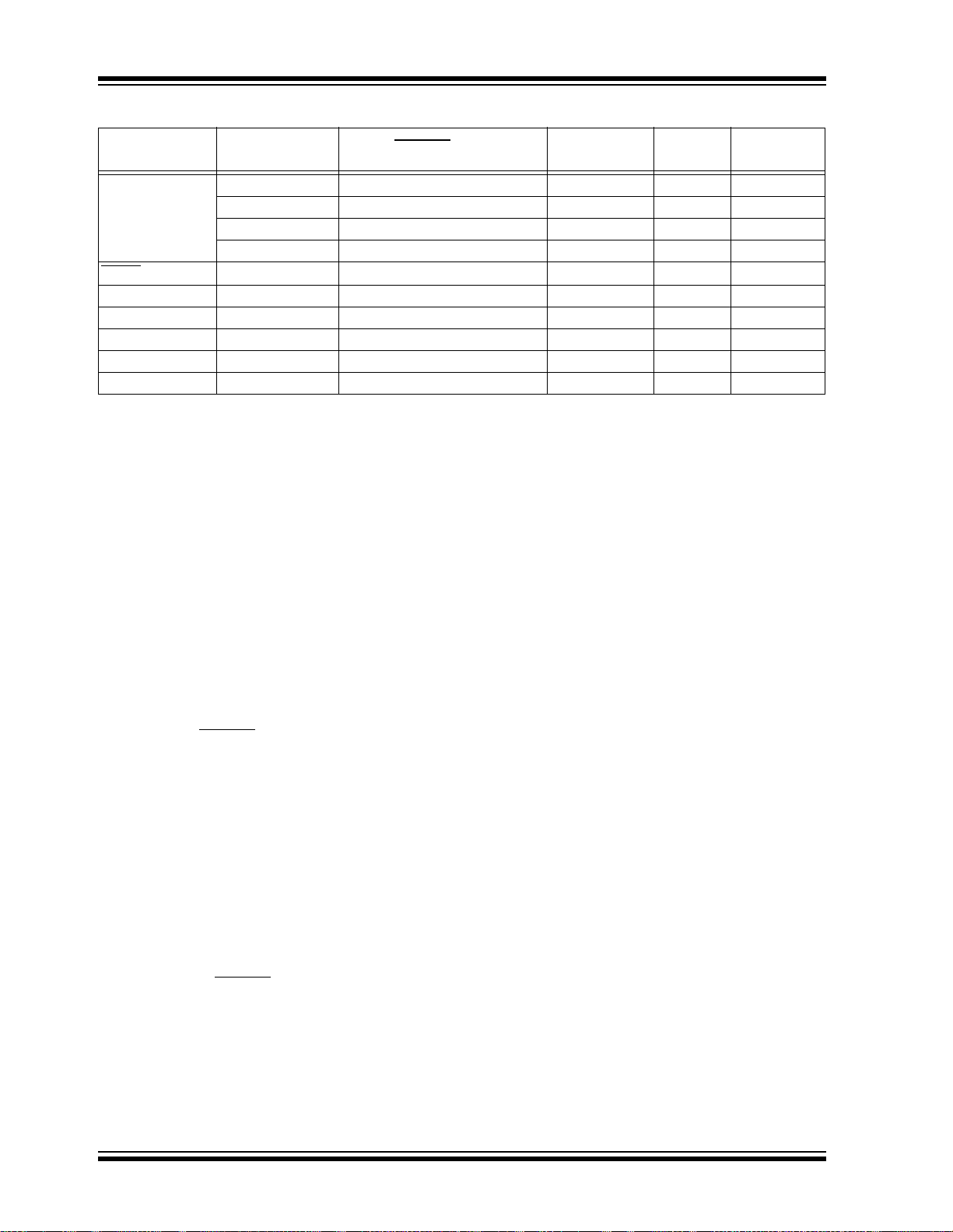
dsPIC33F
TABLE 5-3: RESET DELAY TIMES FOR VARIOUS DEVICE RESETS
Reset Type Clock Source SYSRST
POR
POR EC, FRC, LPRC T
ECPLL, FRCPLL TPOR + TSTARTUP + TRST TLOCK TFSCM 1, 2, 3, 5, 6
XT, HS, SOSC T
XTPLL, HSPLL TPOR + TSTARTUP + TRST TOST + TLOCK TFSCM 1, 2, 3, 4, 5, 6
MCLR
WDT Any Clock TRST ——3
Software Any Clock T
Illegal Opcode Any Clock TRST ——3
Uninitialized W Any Clock TRST ——3
Trap Conflict Any Clock T
Note 1: TPOR = Power-on Reset delay (10 μs nominal).
2: T
Power-up Timer delay (if regu lator is disa bled). T
states, including waking from Sleep mode, only if the regulator is enabled.
3: T
4: TOST = Oscillator Start-up Timer. A 10-bit counter counts 1024 oscillator periods before releasing the
oscillator clock to the system.
5: T
6: T
Any Clock TRST ——3
STARTUP = Conditional POR delay of 20 μs nominal (if on-chip regulator is enabled) or 64 ms nominal
RST = Internal state Reset time (20 μs nominal).
LOCK = PLL lock time (20 μs nominal).
FSCM = Fail-Safe Clock Monitor delay (100 μs nom in al).
+ TSTARTUP + TRST ——1, 2, 3
POR
+ TSTARTUP + TRST TOST TFSCM 1, 2, 3, 4, 6
Delay
RST ——3
RST ——3
STARTUP is also applie d to a ll returns from powered-down
System Clock
Delay
FSCM
Delay
Notes
5.2.1 POR AND LONG OSCILLATOR START-UP TIMES
The oscillator st art-up circui try and its associat ed delay
timers are not linked to the device Reset delays that
occur at power-up. Some crystal circuits (especially
low-frequency crystals) have a relatively long start-up
time. Therefore, one or more of the following con ditions
is possible after SYSRST
• The oscillator circuit has not begun to oscillate.
• The Oscillator Start-up Timer has not expired (if a
crystal oscillator is used).
• The PLL has not achieved a lock (if PLL is used).
The device will not begin to execute code until a valid
clock source has been released to the system. Therefore, the oscillator and PLL start-up delays must be
considered when th e Reset del ay time mu st be known.
is released:
5.2.2 FAIL-SAFE CLOCK MONITOR (FSCM) AND DEVICE RESETS
If the FSCM is enable d, it be gins t o moni tor the s ystem
clock source when SYSRST
source is not available at this time, the device automatically switches to the FRC oscillator and the user
can switch to the desired crystal oscillator in the Trap
Service Routine.
is released. If a valid cloc k
5.2.2.1 FSCM Delay for Crystal and PLL
Clock Sources
When the system clock source is provided by a crystal
oscillator and/or the PL L, a small delay, T
matically inserted after the POR and PWRT delay
times. The FSCM does not be gin to monitor the system
clock source un til th is del ay expi res. Th e FSCM d elay
time is nominally 100 μs and provides additional time
for the oscillator and/ or PLL to st abil ize. In mos t cases ,
the FSCM delay prevents an oscillator failure trap at a
device Reset when the PWRT is disab le d.
FSCM, is auto-
5.3 Special Function Register Reset
States
Most of the Special Function Registers (SFRs) associated with the CPU and peripherals are reset to a
particular value at a device Reset. The SFRs are
grouped by their peripheral or CPU function and their
Reset values ar e specified in ea ch section of th is manual.
The Reset value for each SFR do es not de pend on th e
type of Reset, with the exception of two registers. The
Reset value for the Reset Control register, RCON,
depends on the type of device R eset. The Reset value
for the Oscillator Control register, OSCCON, depends
on the type of Res et and th e programme d values of the
oscillator Configuration bits in the FOSC Configuration
register.
DS70165E-page 86 Preliminary © 2007 Microchip Technology Inc.
Page 89

dsPIC33F
6.0 INTERRUPT CONTROLLER
Note: This data sheet summarizes the features
of this group of dsPIC33F devices. It is not
intended to be a compr ehensive refer ence
source. To complement the information in
this data sheet, refer to the “dsPIC30F
Family Reference Manual” (DS70046).
The dsPIC33F interrupt controller reduces the numerous peripheral interrupt request signals to a single
interrupt request signal to the dsPIC33F CPU. It has
the following features:
• Up to 8 processor exceptions and software traps
• 7 user-selectable priority levels
• Interrupt Vector Table (IVT) with up to 118 vectors
• A unique vector for each interrupt or exception
source
• Fixed priority within a specified user priority level
• Alternate Interrupt Vector Table (AIVT) for debug
support
• Fixed interrupt entry and return latencies
6.1 Interrupt Vector Table
The Interrupt V ect or Table (IVT) is shown in F igure 6-1.
The IVT resides in program memory, starting at location
000004h. The IVT contains 126 vectors consisting of
8 nonmaskable trap vectors plus up to 118 sources of
interrupt. In general, each interrupt source has its own
vector. Each interrupt vector contains a 24-bit wide
address. The value programmed into each interrupt
vector location is th e starti ng address of th e assoc iated
Interrupt Service Routine (ISR).
Interrupt vectors are prioritized in terms of their natural
priority; this priority is linked to their position in the
vector table. All other things being equal, lower
addresses have a higher natural priority. For example,
the interrupt associated with vector 0 will take priority
over interrupts at any other vector address.
dsPIC33F devices implement up to 67 unique
interrupts and 5 nonmaskable traps. These are
summarized in Table 6-1 and Table 6-2.
6.1.1 ALTERNATE VECTOR TABLE
The Alternate Interrupt Vector Table (AIVT) is located
after the IVT, as shown in Figure 6-1. Access to the
AIVT is provided by the ALTIVT control bit
(INTCON2<15>). If the ALTIVT bit is set, all interrupt
and exception processes use the alternate vectors
instead of the defa ult vecto rs. The altern ate vecto rs are
organized in the same manner as the default vectors.
The AIVT support s deb ugg ing by providing a means to
switch between an application and a support environment without requiring the interrupt vectors to be
reprogrammed. This feature also enables switching
between applications for evaluation of different software algorithms at run time. If the AIVT is not needed,
the AIVT should be programmed with the same
addresses used in the IVT.
6.2 Reset Sequence
A device Reset is not a true exception because the
interrupt controller is not inv olved in the Reset pr ocess.
The dsPIC33F de vice clea rs its registers in response to
a Reset, which forces the PC to ze ro. T he digi tal signa l
controller then begins program execution at location
0x000000. The user program s a GOTO instruction at the
Reset address which redirects program execution to
the appropriate start-up routine.
Note: Any unimplemented or unused vector
locations in the IVT and AIVT should be
programmed with the address of a default
interrupt handler routine that contains a
RESET instruction.
© 2007 Microchip Technology Inc. Preliminary DS70165E-page 87
Page 90

dsPIC33F
FIGURE 6-1: dsPIC33F INTERRUPT VECTOR TABLE
Reset – GOTO Instruction 0x000000
Reset – GOTO Address 0x000002
Reserved 0x000004
Oscillator Fail Trap Vector
Address Error Trap Vector
Stack Error Trap Vector
Math Error Trap Vector
DMA Error Trap Vector
Reserved
Reserved
Interrupt Vector 0 0x000014
Interrupt Vector 1
~
~
Interrupt Vector 52 0x00007C
Interrupt Vector 53 0x00007E
Interrupt Vector 54 0x000080
Interrupt Vector 116 0x0000FC
Interrupt Vector 117 0x0000FE
Oscillator Fail Trap Vector
Decreasing Natural Order Priority
Address Error Trap Vector
Stack Error Trap Vector
Math Error Trap Vector
DMA Error Trap Vector
Interrupt Vector 52 0x00017C
Interrupt Vector 53 0x00017E
Interrupt Vector 54 0x000180
Interrupt Vector 116
Interrupt Vector 117 0x0001FE
~
~
~
~
Reserved
Reserved 0x000102
Reserved
Reserved
Reserved
Interrupt Vector 0 0x000114
Interrupt Vector 1
~
~
~
~
~
~
Start of Code 0x000200
0x000100
Interrupt Vector Table (IVT)
Alternate Interrupt Vector Table (AIVT)
(1)
(1)
Note 1: See Table 6-1 for the list of implemented interrupt vectors.
DS70165E-page 88 Preliminary © 2007 Microchip Technology Inc.
Page 91

dsPIC33F
TABLE 6-1: INTERRUPT VECTORS
Vector
Number
8 0 0x000014 0x000114 INT0 – External Interrupt 0
9 1 0x000016 0x000116 IC1 – Input Compare 1
10 2 0x000018 0x000118 OC1 – Output Compare 1
11 3 0x00001A 0x00011A T1 – Timer1
12 4 0x00001C 0x00011C DMA0 – DMA Channel 0
13 5 0x00001E 0x00011E IC2 – Input Capture 2
14 6 0x000020 0x000120 OC2 – Output Compare 2
15 7 0x000022 0x000122 T2 – Timer2
16 8 0x000024 0x000124 T3 – Timer3
17 9 0x000026 0x000126 SPI1E – SPI1 Error
18 10 0x000028 0x000128 SPI1 – SPI1 Transfer Done
19 11 0x00002A 0x00012A U1RX – UART1 Receiver
20 12 0x00002C 0x00012C U1TX – UART1 Transmitter
21 13 0x00002E 0x00012E ADC1 – ADC 1
22 14 0x000030 0x000130 DMA1 – DMA Channel 1
23 15 0x000032 0x000132 Reserved
24 16 0x000034 0x000134 SI2C1 – I2C1 Slave Events
25 17 0x000036 0x000136 MI2C1 – I2C1 Master Events
26 18 0x000038 0x000138 Reserved
27 19 0x00003A 0x00013A Change Notification Interrupt
28 20 0x00003C 0x00013C INT1 – External Interrupt 1
29 21 0x00003E 0x00013E ADC2 – ADC 2
30 22 0x000040 0x000140 IC7 – Input Capture 7
31 23 0x000042 0x000142 IC8 – Input Capture 8
32 24 0x000044 0x000144 DMA2 – DMA Channel 2
33 25 0x000046 0x000146 OC3 – Output Compare 3
34 26 0x000048 0x000148 OC4 – Output Compare 4
35 27 0x00004A 0x00014A T4 – Timer4
36 28 0x00004C 0x00014C T5 – Timer5
37 29 0x00004E 0x00014E INT2 – External Interrupt 2
38 30 0x000050 0x000150 U2RX – UART2 Receiver
39 31 0x000052 0x000152 U2TX – UART2 Transmitter
40 32 0x000054 0x000154 SPI2E – SPI2 Error
41 33 0x000056 0x000156 SPI1 – SPI1 Transfer Done
42 34 0x000058 0x000158 C1RX – ECAN1 Receive Data Ready
43 35 0x00005A 0x00015A C1 – ECAN1 Event
44 36 0x00005C 0x00015C DMA3 – DMA Channel 3
45 37 0x00005E 0x00015E IC3 – Input Capture 3
46 38 0x000060 0x000160 IC4 – Input Capture 4
47 39 0x000062 0x000162 IC5 – Input Capture 5
48 40 0x000064 0x000164 IC6 – Input Capture 6
49 41 0x000066 0x000166 OC5 – Output Compare 5
50 42 0x000068 0x000168 OC6 – Output Compare 6
51 43 0x00006A 0x00016A OC7 – Output Compare 7
52 44 0x00006C 0x00016C OC8 – Output Compare 8
53 45 0x00006E 0x00016E Reserved
Interrupt
Request (IRQ)
Number
IVT Address AIVT Address Interrupt Source
© 2007 Microchip Technology Inc. Preliminary DS70165E-page 89
Page 92

dsPIC33F
TABLE 6-1: INTERRUPT VECTORS (CONTINUED)
Vector
Number
54 46 0x000070 0x000170 DMA4 – DMA Channel 4
55 47 0x000072 0x000172 T6 – Timer6
56 48 0x000074 0x000174 T7 – Timer7
57 49 0x000076 0x000176 SI2C2 – I2C2 Slave Events
58 50 0x000078 0x000178 MI2C2 – I2C2 Master Events
59 51 0x00007A 0x00017A T8 – Timer8
60 52 0x00007C 0x00017C T9 – Timer9
61 53 0x00007E 0x00017E INT3 – External Interrupt 3
62 54 0x000080 0x000180 INT4 – External Interrupt 4
63 55 0x000082 0x000182 C2RX – ECAN2 Receive Data Ready
64 56 0x000084 0x000184 C2 – ECAN2 Event
65 57 0x000086 0x000186 PWM – PWM Period Match
66 58 0x000088 0x000188 QEI – Position Counter Compare
67 59 0x00008A 0x00018A DCIE – DCI Error
68 60 0x00008C 0x00018C DCID – DCI Transfer Done
69 61 0x00008E 0x00018E DMA5 – DMA Channel 5
70 62 0x000090 0x000190 Reserved
71 63 0x000092 0x000192 FLTA
72 64 0x000094 0x000194 FLTB – MCPWM Fault B
73 65 0x000096 0x000196 U1E – UART1 Error
74 66 0x000098 0x000198 U2E – UART2 Error
75 67 0x00009A 0x00019A Reserved
76 68 0x00009C 0x00019C DMA6 – DMA Channel 6
77 69 0x00009E 0x00019E DMA7 – DMA Channel 7
78 70 0x0000A0 0x0001A0 C1TX – ECAN1 Transmit Data Request
79 71 0x0000A2 0x0001A2 C2TX – ECAN2 Transmit Data Request
80-125 72-117 0x0000A4-
Interrupt
Request (IRQ)
Number
IVT Address AIVT Address Interrupt Source
– MCPWM Fault A
0x0000FE
0x0001A4-
0x0001FE
Reserved
TABLE 6-2: TRAP VECTORS
Vector Number IVT Address AIVT Address Trap Source
0 0x000004 0x000084 Reserved
1 0x000006 0x000086 Oscillator Failure
2 0x000008 0x000088 Address Error
3 0x00000A 0x00008A St ac k Error
4 0x00000C 0x00008C Math Error
5 0x00000E 0x00008E DMA Error Trap
6 0x000010 0x000090 Reserved
7 0x000012 0x000092 Reserved
DS70165E-page 90 Preliminary © 2007 Microchip Technology Inc.
Page 93

dsPIC33F
6.3 Interrupt Control and Status Registers
dsPIC33F devices implement a total of 30 registers for
the interrupt controller:
• INTCON1
• INTCON2
• IFS0 through IFS4
• IEC0 through IEC4
• IPC0 through IPC17
•INTTREG
Global interrupt control functions are controlled from
INTCON1 and IN TCON2 . INT CON1 cont ain s the Interrupt Nesting Disa ble (NSTDIS) b it as well as the co ntrol
and status flags for the processor trap sources. The
INTCON2 register controls the external interrupt
request signal behavior and the use of the Alternate
Interrupt Vector Table.
The IFS registers maintain all of the interrupt request
flags. Each source of interr upt has a S tat us bit, which is
set by the respect ive periph erals or exter nal si gnal an d
is cleared v ia software.
The IEC registers maintain all of the interrupt enable
bits. These control bits are used to individually enable
interrupts from the peripherals or external signals.
The IPC registers are used to set the interrupt priority
level for each source of interrupt. Each user interrupt
source can be assigned to one of eight priority levels.
The INTTREG register contains the associated interrupt vector number and the new CPU interrupt priority
level, which are latched into vector number (VECNUM<6:0>) and Interrupt level (ILR<3:0>) bit fields in
the INTTREG register. The new interrupt priority level
is the priority of the pending interrupt.
The interrupt sources are assigned to the IFSx, IECx
and IPCx registers in th e s ame se quence that they are
listed in Table 6-1. For example, the INT0 (External
Interrupt 0) is shown as having vector number 8 and a
natural order priority of 0. Thus, the INT0IF bit is found
in IFS0<0>, the INT0IE bit in IEC0< 0>, a nd th e INT0 IP
bits in the first position of IPC0 (IPC0<2:0>).
Although they are not specifically part of the interrupt
control hardware, tw o of the CPU Control registers contain bits that control interrupt functionality. The CPU
STATUS register, SR, contains the IPL<2:0> bits
(SR<7:5>). These bits indi cate the curr ent CPU inter rupt priority level. The user can change the current
CPU priority level by writing to the IPL bits.
The CORCON register contains the IPL3 bit which,
together with IPL<2: 0>, als o ind ic ates th e c urre nt C PU
priority level. IPL3 is a read-onl y bit so that trap ev ents
cannot be masked by the us er software.
All Interrupt registers are described in Register 6-1
through Register6-32, in the following pages.
© 2007 Microchip Technology Inc. Preliminary DS70165E-page 91
Page 94

dsPIC33F
REGISTER 6-1: SR: CPU STATUS REGISTER
(1)
R-0 R-0 R/C-0 R/C-0 R-0 R/C-0 R -0 R/W-0
OA OB SA SB OAB SAB DA DC
bit 15 bit 8
R/W-0
IPL2
(3)
(2)
R/W-0
IPL1
(2)
(3)
R/W-0
IPL0
(2)
(3)
R-0 R/W-0 R/W-0 R/W-0 R/W-0
RA N OV Z C
bit 7 bit 0
Legend:
C = Clear only bit R = Readable bit U = Unimplemented bit, read as ‘0’
S = Set only bit W = Writable bit -n = Value at POR
‘1’ = Bit is set ‘0’ = Bit is cleared x = Bit is unknown
bit 7-5 IPL<2:0>: CPU Interrupt Priority Level Status bits
(1)
111 = CPU Interrupt Priority Level is 7 (15), user interrupts disabled
110 = CPU Interrupt Priority Level is 6 (14)
101 = CPU Interrupt Priority Level is 5 (13)
100 = CPU Interrupt Priority Level is 4 (12)
011 = CPU Interrupt Priority Level is 3 (11)
010 = CPU Interrupt Priority Level is 2 (10)
001 = CPU Interrupt Priority Level is 1 (9)
000 = CPU Interrupt Priority Level is 0 (8)
Note 1: For complete register details, see Register 2-1: “SR: CPU STATUS Register”.
2: The IPL<2:0> bits are concatenated with the IPL<3> bit (CORCON<3>) to form the CPU Interrupt Priority
Level. The value in parentheses indicates the IPL if IPL<3> = 1. User interrupts are disabled when
IPL<3> = 1.
3: The IPL<2:0> Status bits are read-onl y when NSTDIS (INTCON1<15>) = 1.
REGISTER 6-2: CORCON: CORE CONTROL REGISTER
(1)
U-0 U-0 U-0 R/W-0 R/W-0 R-0 R-0 R-0
— — — US EDT DL<2:0>
bit 15 bit 8
R/W-0 R/W-0 R/W-1 R/W-0 R/C-0 R/W-0 R/W-0 R/W-0
SATA SATB SATDW ACCSAT IPL3
(2)
PSV RND IF
bit 7 bit 0
Legend: C = Clear only bit
R = Readable bit W = Writable bit -n = Value at POR ‘1’ = Bit is set
0’ = Bit is cleared ‘x = Bit is unknown U = Unimplemented bit, read as ‘0’
bit 3 IPL3: CPU Interrupt Priority Level Status bit 3
(2)
1 = CPU interrupt priority level is greater than 7
0 = CPU interrupt priority level is 7 or less
Note 1: For complete register details, see Register 2-2: “CORCON: CORE Control Register”.
2: The IPL3 bit is concatenated with the IPL<2:0> bits (SR<7:5>) to form the CPU Interrupt Priority Level.
DS70165E-page 92 Preliminary © 2007 Microchip Technology Inc.
Page 95

dsPIC33F
REGISTER 6-3: INTCON1: INTERRUPT CONTROL REGISTER 1
R/W-0 R/W-0 R/W-0 R/W-0 R/W-0 R/W-0 R/W-0 R/W-0
NSTDIS OVAERR OVBERR COVAERR COVBERR OVATE OVBTE COVTE
bit 15 bit 8
R/W-0 R/W-0 R/W-0 R/W-0 R/W-0 R/W-0 R/W-0 U-0
SFTACERR DIV0ERR DMACERR MATHERR ADDRERR STKERR OSCFAIL
bit 7 bit 0
Legend:
R = Readable bit W = Writable bit U = Unimplemented bit, read as ‘0’
-n = Value at POR ‘1’ = Bit is set ‘0’ = Bit is cleared x = Bit is unknown
bit 15 NSTDIS: Interrupt Nesting Disable bit
1 = Interrupt nesting is disabled
0 = Interrupt nesting is enabled
bit 14 OVAERR: Accumulator A Overflow Trap Flag bit
1 = Trap was caused by overflow of Accumulator A
0 = Trap was not caused by overflow of Accumulator A
bit 13 OVBERR: Accumulator B Overflow Trap Flag bit
1 = Trap was caused by overflow of Accumulator B
0 = Trap was not caused by overflow of Accumulator B
bit 12 COVAERR: Accumulator A Catastrophic Overflow Trap Enable bit
1 = Trap was caused by catastrophic overflow of Accumulator A
0 = Trap was not caused by catastrophic overflow of Accumulator A
bit 11 COVBERR: Accumulator B Catastrophic Overflow Trap Enable bit
1 = Trap was caused by catastrophic overflow of Accumulator B
0 = Trap was not caused by catastrophic overflow of Accumulator B
bit 10 OVATE: Accumulator A Overflow Trap Enable bit
1 = Trap overflow of Accumulator A
0 = Trap disabled
bit 9 OVBTE: Accumulator B Overflow Trap Enable bit
1 = Trap overflow of Accumulator B
0 = Trap disabled
bit 8 COVTE: Catastrophic Overflow Trap Enable bit
1 = Trap on catastrophic overflow of Accumulator A or B enabled
0 = Trap disabled
bit 7 SFTACERR: Shift Accumulator Error Status bit
1 = Math error trap was caused by an invalid accumulator shift
0 = Math error trap was not caused by an invalid accumulator shift
bit 6 DIV0ERR: Arithmetic Error Status bit
1 = Math error trap was caused by a divide by zero
0 = Math error trap was not caused by a divide by zero
bit 5 DMACERR: DMA Controller Error Status bit
1 = DMA controller error trap has occurred
0 = DMA controller error trap has not occurred
bit 4 MATHERR: Arithmetic Error Status bit
1 = Math error trap has occurred
0 = Math error trap has not occurred
—
© 2007 Microchip Technology Inc. Preliminary DS70165E-page 93
Page 96

dsPIC33F
REGISTER 6-3: INTCON1: INTERRUPT CONTROL REGISTER 1 (CONTINUED)
bit 3 ADDRERR: Address Error Trap Status bit
1 = Address error trap has occurred
0 = Address error trap has not occurred
bit 2 STKERR: Stack Error Trap Status bit
1 = Stack error trap has occurred
0 = Stack error trap has not occurred
bit 1 OSCFAIL: Oscillator Failure Trap Status bit
1 = Oscillator failure trap has occurred
0 = Oscillator failure trap has not occurred
bit 0 Unimplemented: Read as ‘0’
DS70165E-page 94 Preliminary © 2007 Microchip Technology Inc.
Page 97
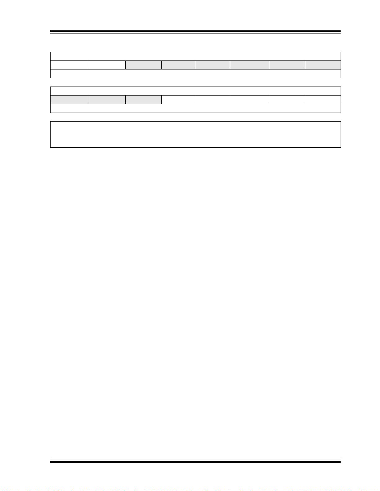
dsPIC33F
REGISTER 6-4: INTCON2: INTERRUPT CONTROL REGISTER 2
R/W-0 R-0 U-0 U-0 U-0 U-0 U-0 U-0
ALTIVT DISI
bit 15 bit 8
U-0 U-0 U-0 R/W-0 R/W-0 R/W-0 R/W-0 R/W-0
— — — INT4EP INT3EP INT2EP INT1EP INT0EP
bit 7 bit 0
Legend:
R = Readable bit W = Writable bit U = Unimplemented bit, read as ‘0’
-n = Value at POR ‘1’ = Bit is set ‘0’ = Bit is cleared x = Bit is unknown
bit 15 ALTIVT: Enable Alternate Interrupt Vector Table bit
1 = Use alternate vector table
0 = Use standard (default) vector table
bit 14 DISI: DISI Instruction Status bit
1 = DISI instruction is active
0 = DISI instruction is not active
bit 13-5 Unimplemented: Read as ‘0’
bit 4 INT4EP: External Interrupt 4 Edge Detect Polarity Select bit
1 = Interrupt on negative edge
0 = Interrupt on positive edge
bit 3 INT3EP: External Interrupt 3 Edge Detect Polarity Select bit
1 = Interrupt on negative edge
0 = Interrupt on positive edge
bit 2 INT2EP: External Interrupt 2 Edge Detect Polarity Select bit
1 = Interrupt on negative edge
0 = Interrupt on positive edge
bit 1 INT1EP: External Interrupt 1 Edge Detect Polarity Select bit
1 = Interrupt on negative edge
0 = Interrupt on positive edge
bit 0 INT0EP: External Interrupt 0 Edge Detect Polarity Select bit
1 = Interrupt on negative edge
0 = Interrupt on positive edge
— — — — — —
© 2007 Microchip Technology Inc. Preliminary DS70165E-page 95
Page 98

dsPIC33F
REGISTER 6-5: IFS0: INTERRUPT FLAG STATUS REGISTER 0
U-0 R/W-0 R/W-0 R/W-0 R/W-0 R/W-0 R/W-0 R/W-0
— DMA1IF AD1IF U1TXIF U1RXIF SPI1IF SPI1EIF T3IF
bit 15 bit 8
R/W-0 R/W-0 R/W-0 R/W-0 R/W-0 R/W-0 R/W-0 R/W-0
T2IF OC2IF IC2IF DMA01IF T1IF OC1IF IC1IF INT0IF
bit 7 bit 0
Legend:
R = Readable bit W = Writable bit U = Unimplemented bit, read as ‘0’
-n = Value at POR ‘1’ = Bit is set ‘0’ = Bit is cleared x = Bit is unknown
bit 15 Unimplemented: Read as ‘0’
bit 14 DMA1IF: DMA Channel 1 Data Transfer Complete Interrupt Flag Status bit
1 = Interrupt request has occurred
0 = Interrupt request has not occurred
bit 13 AD1IF: ADC1 Conversion Complete Interrupt Flag Status bit
1 = Interrupt request has occurred
0 = Interrupt request has not occurred
bit 12 U1TXIF: UART1 Transmitter Interrupt Flag Status bit
1 = Interrupt request has occurred
0 = Interrupt request has not occurred
bit 11 U1RXIF: UART1 Receiver Interrupt Flag Status bit
1 = Interrupt request has occurred
0 = Interrupt request has not occurred
bit 10 SPI1IF: SPI1 Event Interrupt Flag Status bit
1 = Interrupt request has occurred
0 = Interrupt request has not occurred
bit 9 SPI1EIF: SPI1 Fault Interrupt Flag Status bit
1 = Interrupt request has occurred
0 = Interrupt request has not occurred
bit 8 T3IF: Timer3 Interrupt Flag Status bit
1 = Interrupt request has occurred
0 = Interrupt request has not occurred
bit 7 T2IF: Timer2 Interrupt Flag Status bit
1 = Interrupt request has occurred
0 = Interrupt request has not occurred
bit 6 OC2IF: Output Compare Channel 2 Interrupt Flag Status bit
1 = Interrupt request has occurred
0 = Interrupt request has not occurred
bit 5 IC2IF: Input Capture Channel 2 Interrupt Flag Status bit
1 = Interrupt request has occurred
0 = Interrupt request has not occurred
bit 4 DMA0IF: DMA Channel 0 Data Transfer Complete Interrupt Flag Status bit
1 = Interrupt request has occurred
0 = Interrupt request has not occurred
bit 3 T1IF: Timer1 Interrupt Flag Status bit
1 = Interrupt request has occurred
0 = Interrupt request has not occurred
DS70165E-page 96 Preliminary © 2007 Microchip Technology Inc.
Page 99

dsPIC33F
REGISTER 6-5: IFS0: INTERRUPT FLAG STATUS REGISTER 0 (CONTINUED)
bit 2 OC1IF: Output Compare Channel 1 Interrupt Flag Status bit
1 = Interrupt request has occurred
0 = Interrupt request has not occurred
bit 1 IC1IF: Input Capture Channel 1 Interrupt Flag Status bit
1 = Interrupt request has occurred
0 = Interrupt request has not occurred
bit 0 INT0IF: External Interrupt 0 Flag Status bit
1 = Interrupt request has occurred
0 = Interrupt request has not occurred
© 2007 Microchip Technology Inc. Preliminary DS70165E-page 97
Page 100

dsPIC33F
REGISTER 6-6: IFS1: INTERRUPT FLAG STATUS REGISTER 1
R/W-0 R/W-0 R/W-0 R/W-0 R/W-0 R/W-0 R/W-0 R/W-0
U2TXIF U2RXIF INT2IF T5IF T4IF OC4IF OC3IF DMA21IF
bit 15 bit 8
R/W-0 R/W-0 R/W-0 R/W-0 R/W-0 R/W-0 R/W-0 R/W-0
IC8IF IC7IF AD2IF INT1IF CNIF
bit 7 bit 0
Legend:
R = Readable bit W = Writable bit U = Unimplemented bit, read as ‘0’
-n = Value at POR ‘1’ = Bit is set ‘0’ = Bit is cleared x = Bit is unknown
bit 15 U2TXIF: UART2 Transmitter Interrupt Flag Status bit
1 = Interrupt request has occurred
0 = Interrupt request has not occurred
bit 14 U2RXIF: UART2 Receiver Interrupt Flag Status bit
1 = Interrupt request has occurred
0 = Interrupt request has not occurred
bit 13 INT2IF: External Interrupt 2 Flag Status bit
1 = Interrupt request has occurred
0 = Interrupt request has not occurred
bit 12 T5IF: Timer5 Interrupt Flag Status bit
1 = Interrupt request has occurred
0 = Interrupt request has not occurred
bit 11 T4IF: Timer4 Interrupt Flag Status bit
1 = Interrupt request has occurred
0 = Interrupt request has not occurred
bit 10 OC4IF: Output Compare Channel 4 Interrupt Flag Status bit
1 = Interrupt request has occurred
0 = Interrupt request has not occurred
bit 9 OC3IF: Output Compare Channel 3 Interrupt Flag Status bit
1 = Interrupt request has occurred
0 = Interrupt request has not occurred
bit 8 DMA2IF: DMA Channel 2 Data Transfer Complete Interrupt Flag Status bit
1 = Interrupt request has occurred
0 = Interrupt request has not occurred
bit 7 IC8IF: Input Capture Channel 8 Interrupt Flag Status bit
1 = Interrupt request has occurred
0 = Interrupt request has not occurred
bit 6 IC7IF: Input Capture Channel 7 Interrupt Flag Status bit
1 = Interrupt request has occurred
0 = Interrupt request has not occurred
bit 5 AD2IF: ADC2 Conversion Complete Interrupt Flag Status bit
1 = Interrupt request has occurred
0 = Interrupt request has not occurred
bit 4 INT1IF: External Interrupt 1 Flag Status bit
1 = Interrupt request has occurred
0 = Interrupt request has not occurred
— MI2C1IF SI2C1IF
DS70165E-page 98 Preliminary © 2007 Microchip Technology Inc.
 Loading...