


dsPIC30F2011/2012/3012/3013
Data Sheet
High-Performance, 16-Bit
Digital Signal Controllers
© 2006 Microchip Technology Inc. DS70139E
Note the following details of the code protection feature on Microchip devices:
• Microchip products meet the specification contained in their particular Microchip Data Sheet.
• Microchip believes that its family of products is one of the most secure families of its kind on the market today, when used in the
intended manner and under normal conditions.
• There are dishonest and possibly illegal methods used to breach the code protection feature. All of these methods, to our
knowledge, require using the Microchip products in a manner outside the operating specifications contained in Microchip’s Data
Sheets. Most likely, the person doing so is engaged in theft of intellectual property.
• Microchip is willing to work with the customer who is concerned about the integrity of their code.
• Neither Microchip nor any other semiconductor manufacturer can guarantee the security of their code. Code protection does not
mean that we are guaranteeing the product as “unbreakable.”
Code protection is constantly evolving. We at Microchip are committed to continuously improving the code protection features of our
products. Attempts to break Microchip’s code protection feature may be a violation of the Digit al Millennium Copyright Act. If suc h a c t s
allow unauthorized access to your software or other copyrighted work, you may have a right to sue for relief under that Act.
Information contained in this publication regarding device
applications and t he lik e is provided only for your convenience
and may be su perseded by upda t es . It is y our responsibility to
ensure that your application meets with your specifications.
MICROCHIP MAKES NO REPRESENTATIONS OR
WARRANTIES OF ANY KIND WHETHER EXPRESS OR
IMPLIED, WRITTEN OR ORAL, STATUTORY OR
OTHERWISE, RELATED TO THE INFORMATION,
INCLUDING BUT NOT LIMITED TO ITS CONDITION,
QUALITY, PERFORMANCE, MERCHANTABILITY OR
FITNESS FOR PURPOSE. Microchip disclaims all liability
arising from this information and its use. Use of Microchip
devices in life supp ort and/or safety ap plications is entir ely at
the buyer’s risk, and the buyer agrees to defend, indemnify and
hold harmless M icrochip from any and all dama ges, claims,
suits, or expenses re sulting from such use. No licens es are
conveyed, implicitly or otherwise, under any Microchip
intellectual property rights.
Trademarks
The Microchip name and logo, the Microchip logo, Accuron,
dsPIC, K
EELOQ, microID, MPLAB, PIC, PIC, PICSTART ,
PRO MATE, PowerSmart, rfPIC and SmartShunt are
registered trademarks of Microchip Technology Incorporated
in the U.S.A. and other countries.
AmpLab, FilterLab, Migratable Memory, MXDEV, MXLAB,
SEEVAL, SmartSensor and The Embedded Control Solutions
Company are registered trademarks of Microchip Technology
Incorporated in the U.S.A.
Analog-for-the-Digital Age, Application Maestro, CodeGuard,
dsPICDEM, dsPICDEM.net, dsPICworks, ECAN,
ECONOMONITOR, FanSense, FlexROM, fuzzyLAB,
In-Circuit Serial Programming, ICSP, ICEPIC, Linear Active
Thermistor, Mindi, MiWi, MPASM, MPLIB, MPLINK, PICkit,
PICDEM, PICDEM.net, PICLAB, PICtail, PowerCal,
PowerInfo, PowerMate, PowerTool, REAL ICE, rfLAB,
rfPICDEM, Select Mode, Smart Serial, SmartT el, Total
Endurance, UNI/O, WiperLock and ZENA are trademarks of
Microchip Technology Incorporated in the U.S.A. and other
countries.
SQTP is a service mark of Microchip Technology Incorporated
in the U.S.A.
All other trademarks mentioned herein are property of their
respective companies.
© 2006, Microchip Technology Incorporated, Printed in the
U.S.A., All Rights Reserved.
Printed on recycled paper.
Microchip received ISO/TS-16949:2002 certification for its worldwide
headquarters, design and wafer fabrication facilities in Chandler and
Tempe, Arizona, Gresham, Oregon and Mountain View, California. The
Company’s quality system processes and procedures are for its PIC
8-bit MCUs, KEELOQ
microperipherals, nonvolatile memory and analog products. In addition,
Microchip’s quality system for the design and manufacture of
development systems is ISO 9001:2000 certified.
®
code hopping devices, Serial EEPROMs,
DS70139E-page ii © 2006 Microchip Technology Inc.
®

dsPIC30F2011/2012/3012/3013
dsPIC30F201 1/2012/3012/3013 High-Performance
Digital Signal Controllers
Note: This data sheet summarizes features of this g roup
of dsPIC30F devices and is not intended to be a complete
reference source. For more information on the CPU,
peripherals, register descriptions and general device
functionality, refer to the “dsPIC30F Family Reference
Manual” (DS70046). For more informat ion on the device
instruction set and programming, refer to the “dsPIC30F/
33F Programmer’s Reference Manual” (DS70157).
High-Performance Modified RISC CPU:
• Modified Harvard architecture
• C compiler optimized instruction set architecture
• Flexible addressing modes
• 83 base instructions
• 24-bit wide instructions, 16-bit wide data path
• Up to 24 Kbytes on-chip Flash program space
• Up to 2 Kbytes of on-chip data RAM
• Up to 1 Kbytes of nonvolatile data EEPROM
• 16 x 16-bit working register array
• Up to 30 MIPS operation:
- DC to 40 MHz external clock input
- 4 MHz - 10 MHz oscillator input with
PLL active (4x, 8x, 16x)
• Up to 21 interrupt sources:
- 8 user-selectable priority levels
- 3 external interrupt sources
- 4 proce ssor trap sources
DSP Features:
• Dual data fetch
• Modulo and Bit-Reversed modes
• Two 40-bit wide accumulators with optional
saturation logic
• 17-bit x 17-bit single-cycle hardw are frac tio nal /
integer multiplier
• All DSP instructions are single cycle
- Multiply-Accumulate (MAC) operation
• single-cycle ±16 shift
Peripheral Features:
• High-current sink/source I/O pins: 25 mA/25mA
• Three 16-bit timers/counters; optionally pair up
16-bit timers into 32-bit timer modules
• 16-bit Capture input functions
• 16-bit Compare/PWM output functions
• 3-wire SPI modules (supports four Frame modes)
2
•I
C™ module supports Multi-Master/Slave mode
and 7-bit/10-bit addressing
• Up to two addressable UART modules with FIFO
buffers
Analog Features:
• 12-bit Analog-to-Digital Converter (ADC) with:
- 200 ksps conversion rate
- Up to 10 input channels
- Conversion available during Sleep and Idle
• Programmable Low-Voltage Detection (PLVD)
• Programmable Brown-out Reset
Special Microcontroller Features:
• Enhanced Flash program memory:
- 10,000 erase/write cycle (min.) for
industrial temperature range, 100K (typical)
• Data EEPROM memory:
- 100,000 erase/write cycle (min.) for
industrial temperature range, 1M (typical)
• Self-reprogrammable under software control
• Power-on Reset (POR), Power-up Timer (PWR T)
and Oscillator Start-up Timer (OST)
• Flexible Watchdog Timer (WDT) with on-chip lowpower RC oscillator for reliable operation
• Fail-Safe Clock Monitor opera t ion :
- Detects clock failure and switches to on-chip
low-power RC oscillator
• Programmable code protection
• In-Circuit Serial Programming™ (ICSP™)
• Selectable Power Management modes:
- Sleep, Idle and Alternate Clock modes
CMOS Technology:
• Low-power, high-speed Flash technology
• Wide operating voltage range (2.5V to 5.5V)
• Industrial and Extended temperature ranges
• Low-power consumption
© 2006 Microchip Technology Inc. DS70139E-page 1
dsPIC30F2011/2012/3012/3013
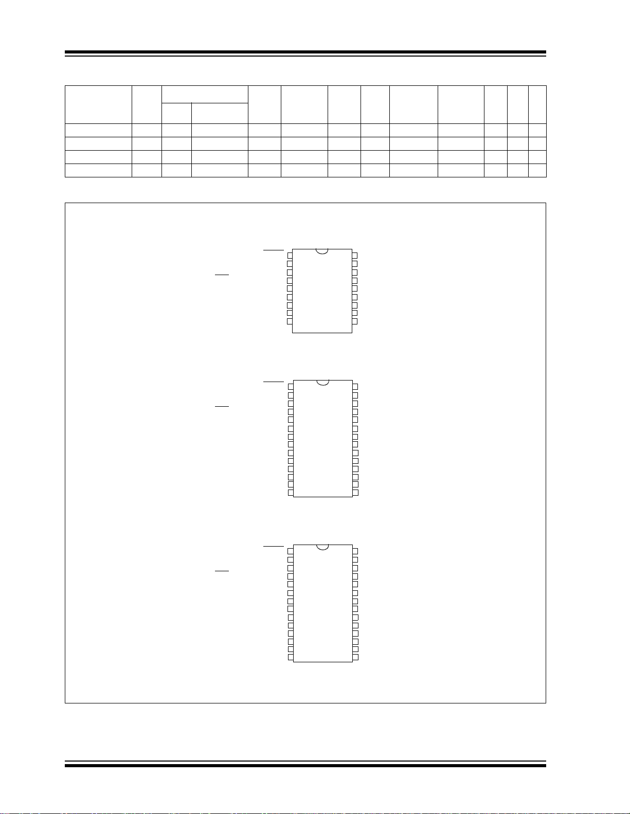
dsPIC30F2011/2012/3012/3013 Sensor Family
Program Memory
Device Pins
Bytes Instructions
SRAM
Bytes
EEPROM
Bytes
Timer
16-bit
Input
Cap
dsPIC30F2011 18 12K 4K 1024 – 3 2 2 8 ch 1 1 1
dsPIC30F3012 18 24K 8K 2048 1024 3 2 2 8 ch 1 1 1
dsPIC30F2012 28 12K 4K 1024 – 3 2 2 10 ch 1 1 1
dsPIC30F3013 28 24K 8K 2048 1024 3 2 2 10 ch 2 1 1
Pin Diagrams
18-Pin PDIP and SOIC
Output
Comp/Std
PWM
A/D 12-bit
200 Ksps
UART
SPI
C™
2
I
EMUD3/AN0/VREF+/CN2/RB0
EMUC3/AN1/VREF-/CN3/RB1
EMUD1/SOSCI/T2CK/U1ATX/CN1/RC13
EMUC1/SOSCO/T1CK/U1ARX/CN0/RC14
28-Pin PDIP and SOIC
EMUD3/AN0/VREF+/CN2/RB0
EMUC3/AN1/V
EMUD1/SOSCI/T2CK/U1ATX/CN1/RC13
EMUC1/SOSCO/T1CK/U1ARX/CN0/RC14
28-Pin SPDIP and SOIC
EMUD3/AN0/VREF+/CN2/RB0
EMUC3/AN1/V
EMUD1/SOSCI/T2CK/U1ATX/CN1/RC13
EMUC1/SOSCO/T1CK/U1ARX/CN0/RC14
MCLR
AN2/SS1
/LVDIN/CN4/RB2
AN3/CN5/RB3
OSC1/CLKI
OSC2/CLKO/RC15
MCLR
AN2/SS1/LVDIN/CN4/RB2
AN2/SS1/LVDIN/CN4/RB2
REF-/CN3/RB1
AN3/CN5/RB3
AN4/CN6/RB4
AN5/CN7/RB5
IC2/INT2/RD9 EMUC2/IC1/INT1/RD8
REF-/CN3/RB1
AN3/CN5/RB3
AN4/CN6/RB4
AN5/CN7/RB5
OSC2/CLKO/RC15
IC2/INT2/RD9
VSS
OSC1/CLKI V
VDD
MCLR
VSS
OSC1/CLKI
VDD
dsPIC30F3012
dsPIC30F2012
dsPIC30F3013
18
DD
AV
17
AV
SS
16
AN6/SCK1/INT0/OCFA/RB6
15
EMUD2/AN7/OC2/IC2/INT2/RB7
14
DD
V
V
SS
13
PGC/EMUC/AN5/U1RX/SDI1/SDA/CN7/RB5
12
11
PGD/EMUD/AN4/U1TX/SDO1/SCL/CN6/RB4
EMUC2/OC1/IC1/INT1/RD0
10
dsPIC30F2011
AV
DD
28
AVSS
27
AN6/OCFA/RB6
26
EMUD2/AN7/RB7
25
AN8/OC1/RB8
24
AN9/OC2/RB9
23
CN17/RF4
22
CN18/RF5
21
DD
20
SSOSC2/CLKO/RC15
V
19
PGC/EMUC/U1RX/SDI1/SDA/RF2
18
PGD/EMUD/U1TX/SDO1/SCL/RF3
17
SCK1/INT0/RF6
16
15
AV
DD
28
AVSS
27
AN6/OCFA/RB6
26
EMUD2/AN7/RB7
25
AN8/OC1/RB8
24
AN9/OC2/RB9
23
U2RX/CN17/RF4
22
U2TX/CN18/RF5
21
V
DD
20
V
SS
19
PGC/EMUC/U1RX/SDI1/SDA/RF2
18
PGD/EMUD/U1TX/SDO1/SCL/RF3
17
SCK1/INT0/RF6
16
EMUC2/IC1/INT1/RD8
15
1
2
3
4
5
6
7
8
9
1
2
3
4
5
6
7
8
9
10
11
12
13
14
1
2
3
4
5
6
7
8
9
10
11
12
13
14
Note: For descriptions of individual pins, see Section 1.0 “Device Overview”.
DS70139E-page 2 © 2006 Microchip Technology Inc.
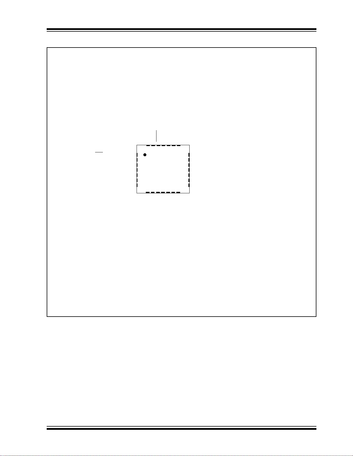
Pin Diagrams
28-Pin QFN
dsPIC30F2011/2012/3012/3013
REF+/CN2/RB0
EMUC3/AN1/VREF-/CN3/RB1
AVDD
AVSS
AN6/SCK1/INT0/OCFA/RB6
EMUD3/AN0/V
MCLR
EMUD2/AN7/OC2/IC2/INT2/RB7
111213
NC
EMUC2/OC1/IC1/INT1/RD0
22
23
NC
21
20
NC
19
NC
NC
18
VDD
17
VSS
16
PGC/EMUC/AN5/U1RX/SDI1/SDA/CN7/RB5
15
14
NC
PGD/EMUD/AN4/U1TX/SDO1/SCL/CN6/RB4
/LVDIN/CN4/RB2
AN2/SS1
OSC2/CLKO/RC15
AN3/CN5/RB3
NC
NC
V
OSC1/CLKI
1
2
3
4
SS
5
6
7
2827262524
dsPIC30F2011
8910
DD
V
EMUD1/SOSC1/T2CK/U1ATX/CN1/RC13
EMUC1/SOSCO/T1CK/U1ARX/CN0/RC14
Note: For descriptions of individual pins, see Section 1.0 “Device Overview”.
© 2006 Microchip Technology Inc. DS70139E-page 3
dsPIC30F2011/2012/3012/3013
Pin Diagrams
28-Pin QFN
REF-/CN3/RB1
AVDD
AVSS
AN6/OCFA/RB6
AN2/SS1/LVDIN/CN4/RB2
AN3/CN5/RB3
AN4/CN6/RB4
AN5/CN7/RB5
V
OSC1/CLKI
OSC2/CLKO/RC15
1
2
3
dsPIC30F2012
4
SS
5
6
7
MCLR
EMUC3/AN1/V
EMUD3/AN0/VREF+/CN2/RB0
26
27
28
10
8
9
25
11
121314
EMUD2/AN7/RB7
22
23
24
21
AN8/OC1/RB8
AN9/OC2/RB9
20
CN17/RF4
19
CN18/RF5
18
V
DD
17
VSS
16
PGC/EMUC/U1RX/SDI1/SDA/RF2
15
DD
V
IC2/INT2/RD9
SCK1/INT0/RF6
EMUC2/IC1/INT1/RD8
PGD/EMUD/U1TX/SDO1/SCL/RF3
EMUD1/SOSCI/T2CK/U1ATX/CN1/RC13
EMUC1/SOSCO/T1CK/U1ARX/CN0/RC14
Note: For descriptions of individual pin s, see Section 1.0 “Device Overview”.
DS70139E-page 4 © 2006 Microchip Technology Inc.
Pin Diagram
44-Pin QFN
PGC/EMUC/AN5/U1RX/SDI1/SDA/CN7/RB5
dsPIC30F2011/2012/3012/3013
DD
EMUC1/SOSCO/T1CK/U1ARX/CN0/RC14
NCNCV
PGD/EMUD/AN4/U1TX/SDO1/SCL/CN6/RB4NCEMUC2/OC1/IC1/INT1/RD0NCNC
4443 424140 393837 3635
1
2 32
SS
V
3
NC
4
DD
V
5
NC
NC
NC
NC
NC
NC
NC
6
7
8
9
10
11
dsPIC30F3012
1213 141516 171819 2021
NC
EMUD1/SOSCI/T2CK/U1ATX/CN1/RC13
34
OSC2/CLKO/RC15
33
OSC1/CLKI
VSS
31
30
SS
V
29
NC
NC
28
NC
27
NC
26
AN3/CN5/RB3
25
24
NC
23
AN2/SS1/LVDIN/CN4/RB2
22
NC
NC
NC
AVSS
AVDD
AN6/SCK1/INT0/OCFA/RB6
EMUD2/AN7/OC2/IC2/INT2/RB7
NC
MCLR
REF-/CN3/RB1
REF+/CN2/RB0
EMUC3/AN1/V
EMUD3/AN0/V
Note: For descriptions of individual pins, see Section 1.0 “Device Overview”.
© 2006 Microchip Technology Inc. DS70139E-page 5
dsPIC30F2011/2012/3012/3013
Pin Diagrams
44-Pin QFN
DD
EMUC1/SOSCO/T1CK/U1ARX/CN0/RC14
NC
IC2/INT2/RD9
V
PGD/EMUD/U1TX/SDO1/SCL/RF3
SCK1/INT0/RF6
EMUC2/IC1/INT1/RD8NCNC
NC
EMUD1/SOSCI/T2CK/U1ATX/CN1/RC13
PGC/EMUC/U1RX/SDI1/SDA/RF2
V
NC
V
NC
NC
U2TX/CN18/RF5
NC
U2RX/CN17/RF4
AN9/OC2/RB9
AN8/OC1/RB8
444342414039383736
1
2 32
SS
3
4
DD
5
6
dsPIC30F3013
7
8
9
10
11
121314151617181920
NC
NC
AVSS
AVDD
AN6/OCFA/RB6
EMUD2/AN7/RB7
35
34
OSC2/CLKO/RC15
33
OSC1/CLKI
VSS
31
SS
V
30
29
NC
NC
28
AN5/CN7/RB5
27
AN4/CN6/RB4
26
AN3/CN5/RB3
25
NC
24
AN2/SS1/LVDIN/CN4/RB2
23
21
22
NC
NC
MCLR
REF-/CN3/RB1
REF+/CN2/RB0
EMUC3/AN1/V
EMUD3/AN0/V
Note: For descriptions of individual pins, see Section 1.0 “Device Overview”.
DS70139E-page 6 © 2006 Microchip Technology Inc.

dsPIC30F2011/2012/3012/3013
Table of Contents
1.0 Device Overview.......................................................................................................................................................................... 9
2.0 CPU Architecture Overview........................................................................................................................................................ 17
3.0 Memory Organization................................................................................................................................................................. 27
4.0 Address Generator Units............................................................................................................................................................ 41
5.0 Flash Program Memory............ ............................................................................. ..................................................................... 47
6.0 Data EEPROM Memory............................................................................................... ..............................................................53
7.0 I/O Ports.................. ................................................................................................................................................................... 57
8.0 Interrupts....................................................................................................................................................................................63
9.0 Timer1 Module ........................................................................................................................................................................... 71
10.0 Timer2/3 Module ........................ .. .... .. .. .. .. ....... .. .. .. .... .. .. .. ....... .. .. .. .. .... .. ..... .... .. .. .. .. .... ..... ............................................................ 75
11.0 Input Capture Module..................................................................... .. .... ....... .. .. .... .. .. .. ....... .......................................................... 81
12.0 Output Compare Module..................................................................................... ....................................................................... 85
13.0 SPI Module.................................................................................................................................................................................89
14.0 I2C Module................................................................................................................................................................................. 93
15.0 Universal Asynchronous Receiver Transmitter (UART) Module .............................................................................................. 101
16.0 12-bit Analog-to-Digital Converter (ADC) Module .................................................................................................................... 109
17.0 System Integration................................... ................................................................................................................................119
18.0 Instruction Set Summary..........................................................................................................................................................133
19.0 Development Support............................................................................................................................................................... 141
20.0 Electrical Characteristics..........................................................................................................................................................145
21.0 Packaging Information. .............................................................................. ............................................................................... 183
Index ..................................................................................................................................................................................................193
The Microchip Web Site..................................................................................................................................................................... 199
Customer Change Notification Service ..............................................................................................................................................199
Customer Support.............................................................................................................................................................................. 199
Reader Response.............................................................................................................................................................................. 200
Product Identification System............................................................................................................................................................201
TO OUR VALUED CUSTOMERS
It is our intention to provide our valued customers with the best documentation possible to ensure successful use of your Microchip
products. To this end, we will continue to improve our publications to better suit your needs. Our publications will be refined and
enhanced as new volumes and updates are introduced.
If you have any questions or c omm ents regarding t his publication, p lease c ontact the M arket ing Co mmunications Department via
E-mail at docerrors@microchip.com or fax the Reader Response Form in the back of this data sheet to (480) 792-4150. We
welcome your feedback.
Most Current Data Sheet
To obtain the most up-to-date version of this data sheet, please register at our Worldwide Web site at:
http://www.microchip.com
You can determine the version of a data sheet by examining its literature number found on the bottom outside corner of any page.
The last character of the literature number is the version number, (e.g., DS30000A is version A of document DS30000).
Errata
An errata sheet, describing minor operational differences from the data sheet and recommended workarounds, may exist for current
devices. As device/documentation issues become known to us, we will publish an errata sheet. The errata will specify the revision
of silicon and revision of document to which it applies.
To determine if an errata sheet exists for a particular device, please check with one of the following:
• Microchip’s Worldwide Web site; http://www.microchip.com
• Your local Microchip sales office (see last page)
When contacting a sales office, please specify which device, revision of silicon and data sheet (include literature number) you are
using.
Customer Notification System
Register on our web site at www.microchip.com to receive the most current information on all of our products.
© 2006 Microchip Technology Inc. DS70139E-page 7

dsPIC30F2011/2012/3012/3013
NOTES:
DS70139E-page 8 © 2006 Microchip Technology Inc.

dsPIC30F2011/2012/3012/3013
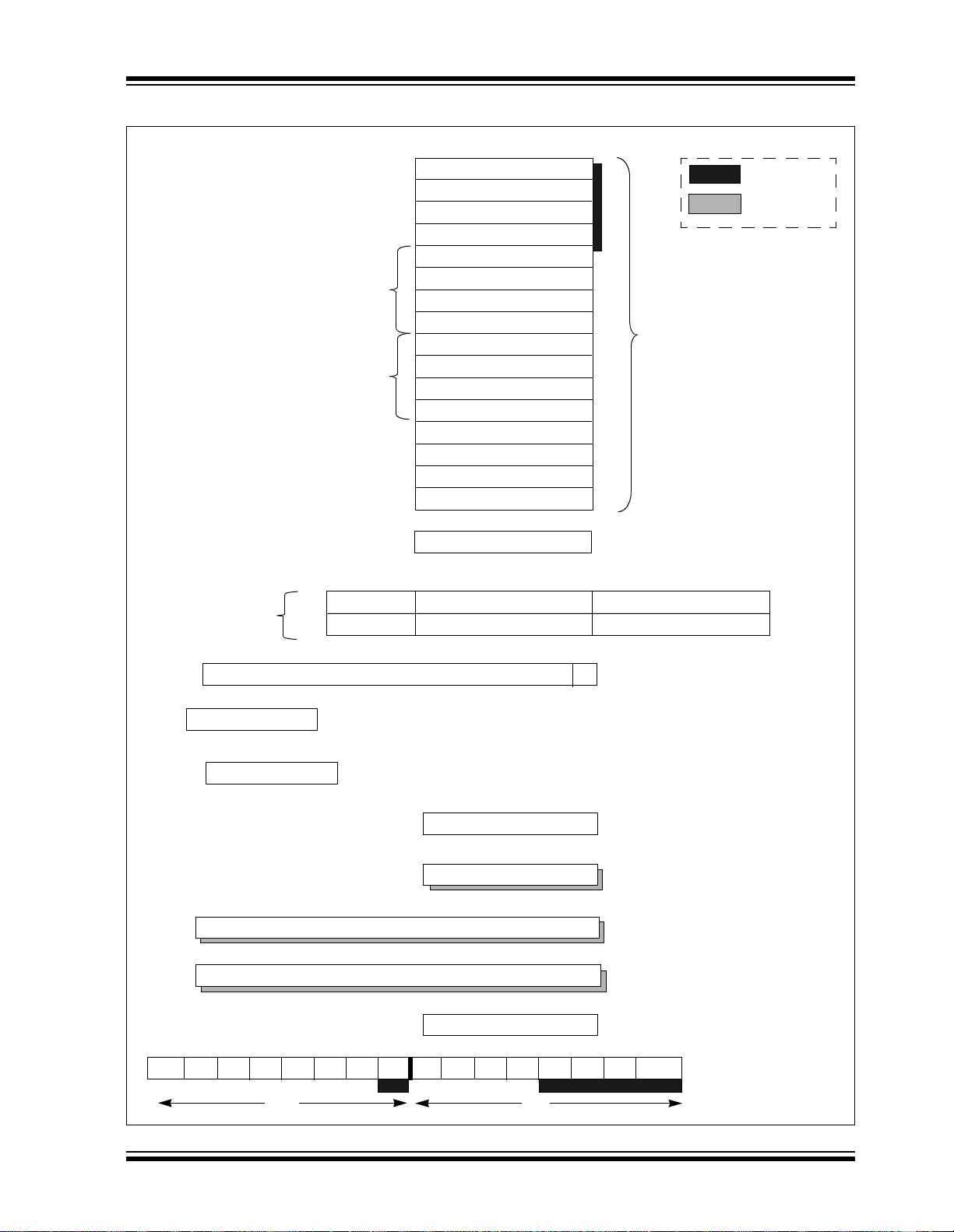
1.0 DEVICE OVERVIEW
Note: This data sheet summarizes features of this group
of dsPIC30F devices and is not intended to be a complete
reference source. For more information on the CPU,
peripherals, register descriptions and general device
functionality, refer to the “dsPIC30F Family Reference
Manual” (DS70046). For more informat ion on the device
instruction set and programming, refer to the “dsPIC30F/
33F Programmer’s Reference Manual“ (DS70157).
This data sheet contains information specific to the
dsPIC30F2011, dsPIC30F2012, dsPIC30F3012 and
dsPIC30F3013 Digit al Signal Controll ers (DSC). These
devices contain extensive Digital Signal Processor
(DSP) functionality within a high-performance 16-bit
microcontroller (MCU) architecture.
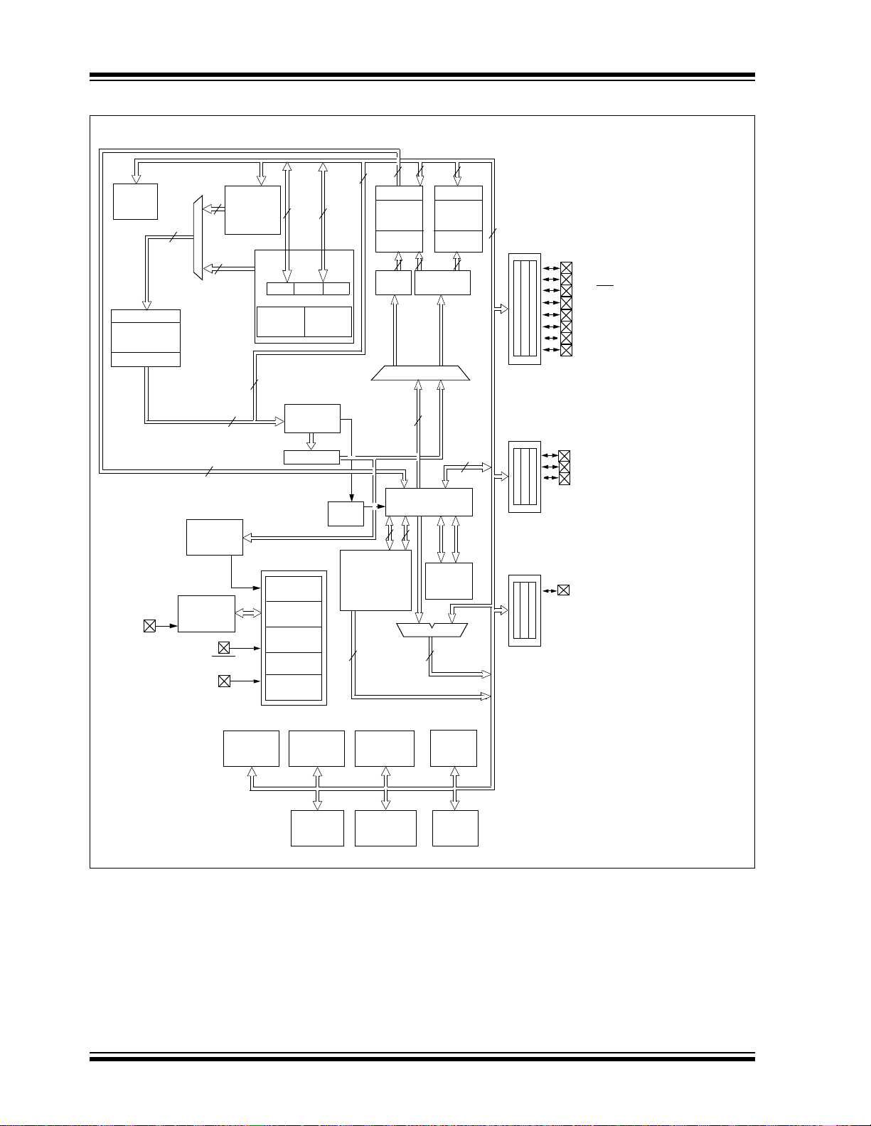
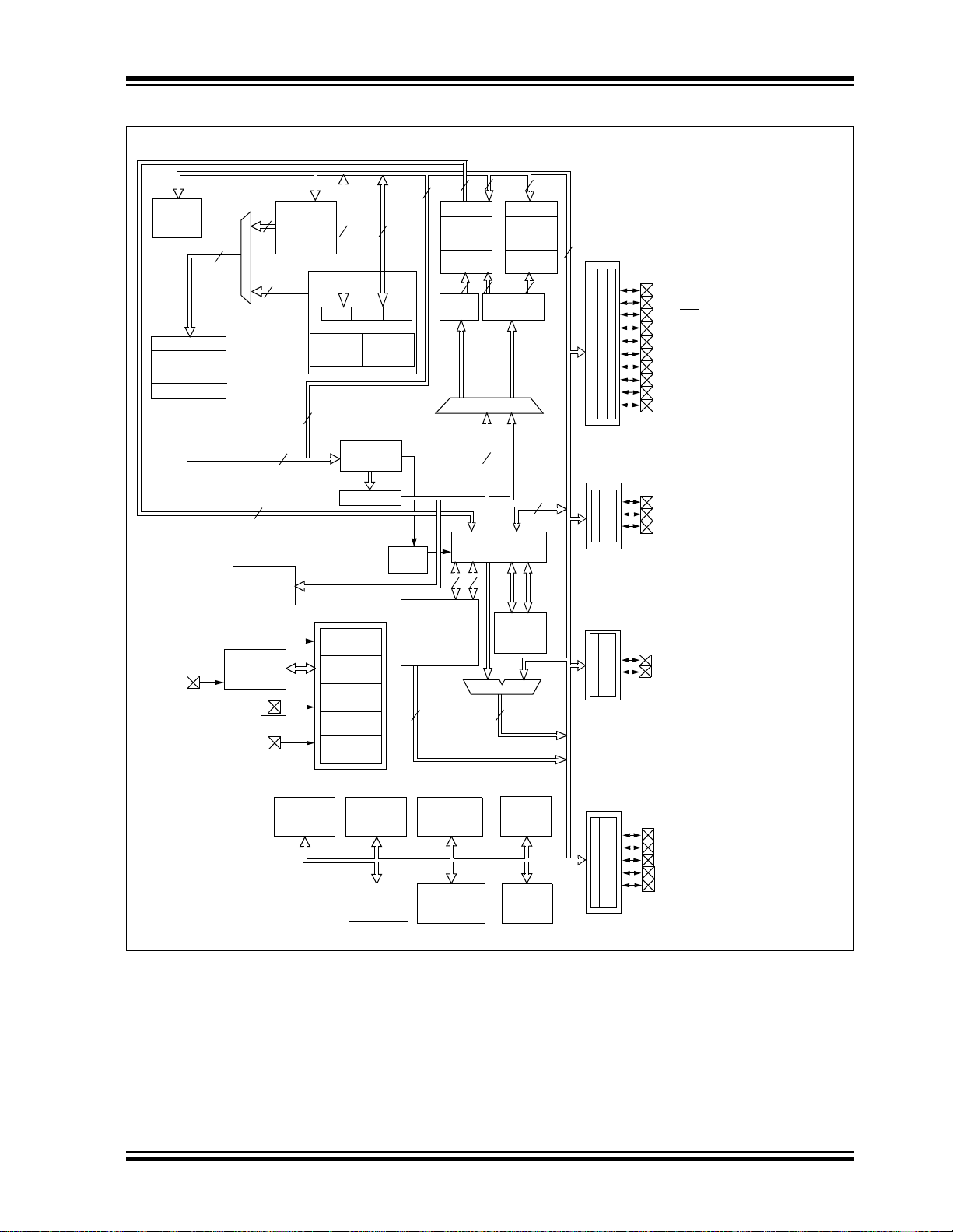
The following block di agrams depict the archi tecture for
these devices:
• Figure 1-1 illustrates the dsPIC30F2011
• Figure 1-2 illustrates the dsPIC30F2012
• Figure 1-3 illustrates the dsPIC30F3012
• Figure 1-4 illustrates the dsPIC30F3013
Following the block d iag ram s, Table 1-1 relates the I/O
functions to pinout information.
© 2006 Microchip Technology Inc. DS70139E-page 9
dsPIC30F2011/2012/3012/3013
FIGURE 1-1: dsPIC30F2011 BLOCK DIAGRAM
Interrupt
Controller
Address Latch
Program Memory
(12 Kbytes)
Data Latch
24
24
Control Block
24
16
Instruction
Decode &
Control
PSV & Table
Data Access
Control
16
24
Y Data Bus
8
16
PCH PCL
PCU
Program Counter
Stack
Logic
ROM Latch
IR
Loop
Control
Logic
Decode
16
16
Y Data
RAM
(512 bytes)
Address
Latch
Y AGU
Effective Address
16
X Data Bus
16
Data LatchData Latch
(512 bytes)
Address
16
16
X RAGU
X WAGU
16
16 x 16
W Reg Array
16
16
X Data
RAM
Latch
16
16
16
PORTB
PORTC
EMUD3/AN0/V
EMUC3/AN1/V
AN2/SS1/LVDIN/CN4/RB2
AN3/CN5/RB3
PGD/EMUD/AN4/U1TX/SDO1/SCL/CN6/RB4
PGC/EMUC/AN5/U1RX/SDI1/SDA/CN7/R
AN6/SCK1/INT0/OCFA/RB6
EMUD2/AN7/OC2/IC2/INT2/RB7
EMUD1/SOSCI/T2CK/U1ATX/CN1/RC13
EMUC1/SOSCO/T1CK/U1ARX/CN0/RC14
OSC2/CLKO/RC15
REF
+/CN2/RB0
REF
-/CN3/RB1
B5
OSC1/CLKI
Timing
Generation
MCLR
VDD, V
AVDD, AV
SS
SS
12-bit ADC
Power-up
Timer
Oscillator
Start-up Timer
POR/BOR
Reset
Watchdog
Timer
Low-Voltage
Detect
Input
Capture
Module
Timers
DSP
Engine
16
Compare
Module
SPI1
Output
Divide
Unit
ALU<16>
16
UART1
EMUC2/OC1/IC1/INT1/RD0
PORTD
I2C™
DS70139E-page 10 © 2006 Microchip Technology Inc.
dsPIC30F2011/2012/3012/3013
FIGURE 1-2: dsPIC30F2012 BLOCK DIAGRAM
Interrupt
Controller
Address Latch
Program Memory
(12 Kbytes)
Data Latch
24
PSV & Table
Data Access
24
Control Block
24
16
Instruction
Decode &
Control
Y Data Bus
16
8
16
PCH PCL
PCU
Program Counter
Stack
Control
Logic
16
24
ROM Latch
IR
Loop
Control
Logic
Decode
Y Data
(512 bytes)
Address
Latch
Y AGU
Effective Address
X Data Bus
16
16 16
Data LatchData Latch
RAM
16
(512 bytes)
16
16
X RAGU
X WAGU
16
16 x 16
W Reg Array
16
X Data
RAM
Address
Latch
16
16
16
PORTB
PORTC
REF
EMUD3/AN0/V
EMUC3/AN1/V
AN2/SS1/LVDIN/CN4/RB2
AN3/CN5/RB3
AN4/CN6/RB4
AN5/CN7/RB5
AN6/OCFA/RB6
EMUD2/AN7/RB7
AN8/OC1/RB8
AN9/OC2/RB9
EMUD1/SOSCI/T2CK/U1ATX/CN1/RC13
EMUC1/SOSCO/T1CK/U1ARX/CN0/RC14
OSC2/CLKO/RC15
+/CN2/RB0
REF
-/CN3/RB1
OSC1/CLKI
Timing
Generation
MCLR
VDD, V
DD
AV
SS
, AV
SS
12-bit ADC
Power-up
Timer
Oscillator
Start-up Timer
POR/BOR
Reset
Watchdog
Timer
Low-Voltage
Detect
Input
Capture
Module
Timers
DSP
Engine
16
Compare
Module
Output
SPI1
Divide
Unit
ALU<16>
16
UART1
I2C™
PORTD
PORTF
EMUC2/IC1/INT1/RD8
IC2/INT2/RD9
PGC/EMUC/U1RX/SDI1/SDA/RF2
PGD/EMUD/U1TX/SDO1/SCL/RF3
CN17/RF4
CN18/RF5
SCK1/INT0/RF6
© 2006 Microchip Technology Inc. DS70139E-page 11

dsPIC30F2011/2012/3012/3013
FIGURE 1-3: dsPIC30F3012 BLOCK DIAGRAM
Interrupt
Controller
Address Latch
Program Memory
(24 Kbytes)
Data EEPROM
(1 Kbytes)
Data Latch
24
24
Control Block
24
16
Instruction
Decode &
Control
PSV & Table
Data Access
Control
16
24
Y Data Bus
8
16
PCH PCL
PCU
Program Counter
Stack
Logic
ROM Latch
IR
Loop
Control
Logic
Decode
16
16
Y Data
RAM
(1 Kbytes)
Address
Latch
Y AGU
Effective Address
16
X Data Bus
16
Data LatchData Latch
X Data
(1 Kbytes)
Address
Latch
16
16
X RAGU
X WAGU
16
16 x 16
W Reg Array
16
16
RAM
16
16
PORTB
16
PORTC
EMUD3/AN0/V
EMUC3/AN1/V
AN2/SS1/LVDIN/CN4/RB2
AN3/CN5/RB3
PGD/EMUD/AN4/U1TX/SDO1/SCL/CN6/RB4
PGC/EMUC/AN5/U1RX/SDI1/SDA/CN7/R
AN6/SCK1/INT0/OCFA/RB6
EMUD2/AN7/OC2/IC2/INT2/RB7
EMUD1/SOSCI/T2CK/U1ATX/CN1/RC13
EMUC1/SOSCO/T1CK/U1ARX/CN0/RC14
OSC2/CLKO/RC15
REF
+/CN2/RB0
REF
-/CN3/RB1
B5
OSC1/CLKI
Timing
Generation
MCLR
VDD, V
AVDD, AV
SS
SS
12-bit ADC
Power-up
Timer
Oscillator
Start-up Timer
POR/BOR
Reset
Watchdog
Timer
Low-Voltage
Detect
Input
Capture
Module
Timers
DSP
Engine
16
Compare
Module
SPI1
Output
Divide
Unit
ALU<16>
16
UART1
EMUC2/OC1/IC1/INT1/RD0
PORTD
I2C™
DS70139E-page 12 © 2006 Microchip Technology Inc.

dsPIC30F2011/2012/3012/3013
FIGURE 1-4: dsPIC30F3013 BLOCK DIAGRAM
Interrupt
Controller
Address Latch
Program Memory
(24 Kbytes)
Data EEPROM
(1 Kbytes)
Data Latch
24
Data Access
24
Control Block
24
16
Instruction
Decode &
Control
PSV & Table
Control
16
24
Y Data Bus
8
16
PCH PCL
PCU
Program Counter
Stack
Logic
ROM Latch
IR
Loop
Control
Logic
Decode
16
16
Y Data
RAM
(1 Kbytes)
Address
Latch
Y AGU
Effective Address
16
X Data Bus
16
Data LatchData Latch
X Data
(1 Kbytes)
Address
16
16
X RAGU
X WAGU
16
16 x 16
W Reg Array
16
16
RAM
Latch
16
16
PORTB
16
PORTC
EMUD3/AN0/V
EMUC3/AN1/V
AN2/SS1/LVDIN/CN4/RB2
AN3/CN5/RB3
AN4/CN6/RB4
AN5/CN7/RB5
AN6/OCFA/RB6
EMUD2/AN7/RB7
AN8/OC1/RB8
AN9/OC2/RB9
EMUD1/SOSCI/T2CK/U1ATX/CN1/RC13
EMUC1/SOSCO/T1CK/U1ARX/CN0/RC14
OSC2/CLKO/RC15
REF
+/CN2/RB0
REF
-/CN3/RB1
OSC1/CLKI
Timing
Generation
MCLR
VDD, V
DD
AV
SS
, AV
SS
12-bit ADC
Power-up
Timer
Oscillator
Start-up Timer
POR/BOR
Reset
Watchdog
Timer
Low-Voltage
Detect
Input
Capture
Module
Timers
DSP
Engine
16
Output
Compare
Module
SPI1
Divide
Unit
EMUC2/IC1/INT1/RD8
IC2/INT2/RD9
ALU<16>
16
I2C™
UART1,
UART2
PORTD
PORTF
PGC/EMUC/U1RX/SDI1/SDA/RF2
PGD/EMUD/U1TX/SDO1/SCL/RF3
U2RX/CN17/RF4
U2TX/CN18/RF5
SCK1/INT0/RF6
© 2006 Microchip Technology Inc. DS70139E-page 13

dsPIC30F2011/2012/3012/3013
Table 1-1 provides a brief description of device I/O
pinouts and the functions that may be multiplexed to a
port pin. Multiple functions may exist on one port pin.
When multiplexing occurs, the peripheral module’s
functional requirements may force an override of the
data direction of the port pin.
TABLE 1-1: PINOUT I/O DESCRIPTIONS
Pin Name
AN0 - AN9 I Analog Analog input channels.
AV
DD P P Positive supply for analog module.
SS P P Ground reference fo r an al og module.
AV
CLKI
CLKO
CN0 - CN7 I ST Input ch ange notification inputs.
EMUD
EMUC
EMUD1
EMUC1
EMUD2
EMUC2
EMUD3
EMUC3
IC1 - IC2 I ST Capture in puts 1 thr ou gh 2.
INT0
INT1
INT2
LVDIN I Analog Low-Voltage Detect Reference Voltage Input pin.
MCLR
OC1-OC2
OCFA
OSC1
OSC2
PGD
PGC
RB0 - RB9 I/O ST PORTB is a bidirectional I/O port.
RC13 - RC15 I/O ST PORTC is a bidirectional I/O port.
RD0, RD8 - RD9 I/O ST PORTD is a bidirectional I/O port.
RF2 - RF5 I/O ST PORTF is a bidirectional I/O port.
SCK1
SDI1
SDO1
1
SS
Pin
Type
I
O
I/O
I/O
I/O
I/O
I/O
I/O
I/O
I/O
I
I
I
I/P ST Maste r Cl ear (Reset) input or programm i ng voltage input. This
O
I
I
I/O
I/O
I
I/O
I
O
I
Legend: CMOS = CMOS compatible input or out put Analog = Analog input
ST = Schmitt Trigger input with CMOS levels O = Output
I = Input P = Power
Buffer
Type
ST/CMOS—External clock source i nput. Alway s associated with OSC1 pin
function.
Oscillator crystal outp ut . Co nnects to crystal or resonator in
Crystal Oscillator mode. Optionally functions as CLKO in RC
and EC modes. Always ass ociated with OSC2 pin function.
Can be software programmed for internal weak pull-ups on all
inputs.
ST
ST
ST
ST
ST
ST
ST
ST
ST
ST
ST
—
ST
ST/CMOS—Oscillator crystal input. ST buffer when configured in RC mode;
ST
ST
ST
ST
—
ST
ICD Primary Communi cation Channel data input/ou tp ut pi n.
ICD Primary Communication Channel clock input/output pin.
ICD Secondary Communication Channel data input/output pin.
ICD Secondary Comm unication Channel cloc k i nput/output pin.
ICD T ertiary Communication Channel data input/output pin.
ICD Tertiary Communication Channel clock input/output pin.
ICD Quaternary Comm unication Channel data input /o utput pin.
ICD Quaternary Comm unication Channel clock in put / ou tp ut pi n.
External interrupt 0.
External interrupt 1.
External interrupt 2.
pin is an active-low Reset to the device.
Compare outputs 1 through 2.
Compare Fault A input.
CMOS otherwise.
Oscillator crystal outp ut . Co nnects to crystal or resonator in
Crystal Oscillator mode. Optionally functions as CLKO in RC
and EC modes.
In-Circuit Serial Programmi ng™ data input/output pin.
In-Circuit Serial Programmi ng clock input pin.
Synchronous serial clock input/output for SPI1.
SPI1 Data In.
SPI1 Data Out.
SPI1 Slave Synchronization.
Description
DS70139E-page 14 © 2006 Microchip Technology Inc.

dsPIC30F2011/2012/3012/3013
TABLE 1-1: PINOUT I/O DESCRIPTIONS (CONTINUED)
Pin Name
SCL
SDA
SOSCO
SOSCI
T1CK
T2CK
U1RX
U1TX
U1ARX
U1ATX
U2RX
U2TX
DD P — Positive supply for logic and I/O pins.
V
VSS P — Ground reference for logic and I/O pins.
REF+ I Analog Analog Voltage Reference (High) input.
V
VREF- I Analog Analog Voltage Reference (Low) input.
Pin
Type
I/O
I/O
O
I
I
I
I
O
I
O
I
O
Legend: CMOS = CMOS compatible input or out put Analog = Analog input
ST = Schmitt Trigger input with CMOS levels O = Output
I = Input P = Power
Buffer
Type
ST
ST
—
ST/CMOS
ST
ST
ST
—
ST
—
ST
—
Description
Synchronous serial clock input/output for I2C™.
Synchronous serial data inp ut / out put for I
32 kHz low-power oscillator crystal output.
32 kHz low-power oscillator crystal input. ST buffer when
configured in RC mode; C M O S ot her w i se.
Timer1 external clock input.
Timer2 external clock input.
UART1 Receive.
UART1 Transmit.
UART1 Al t ernate Receive.
UART1 Al t ernate Transmit .
UART2 Receive.
UART2 Transmit.
2
C.
© 2006 Microchip Technology Inc. DS70139E-page 15

dsPIC30F2011/2012/3012/3013
NOTES:
DS70139E-page 16 © 2006 Microchip Technology Inc.

dsPIC30F2011/2012/3012/3013
2.0 CPU ARCHITECTURE OVERVIEW
Note: This data sheet summarizes features of this group
of dsPIC30F devices and is not intended to be a complete
reference source. For more information on the CPU,
peripherals, register descriptions and general device
functionality, refer to the “dsPIC30F Family Reference
Manual” (DS70046). For more informat ion on the device
instruction set and programming, refer to the “dsPIC30F/
33F Programmer’s Reference Manual” (DS70157).
This section is an overview of the CPU architecture of
the dsPIC30F. The core has a 24-bit instruction word.
The Program Counter (PC) is 23 bits wide with the
Least Significant bit (LSb) always clear (see
Section 3.1 “Program Address Space”). The Most
Significant bit (MSb) is ignored during normal program
execution, except for certain specialized instructions.
Thus, the PC can address up to 4M instruction words
of user program spac e. An instruction prefetch m e ch anism helps maintain throughput. Program loop constructs, free from loop count management overhead,
are supported using the DO and REPEAT instructions,
both of which are interruptible at any point.
2.1 Core Overview
The working registe r array consis ts of 16 x 16-bit re gisters, each of which can act as data, address or offset
registers. One working register (W15) operates as a
Software Stack Pointer for interrupts and calls.
The data space is 64 Kbytes (32K words) and is split
into two blocks, referred to as X and Y data memory.
Each block has its own independent Address Generation Unit (AGU). Most instructions operate solely
through the X memory, AGU, which provides the
appearance of a single unified data space. The
Multiply-Accu mulate (MAC) class of dual s ource DSP
instructions operate through both the X and Y AGUs,
splitting the data address space into two parts (see
Section 3.2 “Data Address Space”). The X and Y
data space boundary is device specific and cannot be
altered by the user. Each data word consists of 2 bytes
and most instruction s can address da ta either as words
or bytes.
Two ways to access data in program memory are:
• The upper 32 Kbytes of data space memory can
be mapped into the lower half (user space) of
program space at any 16K program word boundary, defined by the 8-bit Program Space Visibility
Page (PSVPAG) register. Thus any instruction
can access program space as if it were data
space, with a limitation that the access requires
an additional cycle. On ly the low er 16 bit s of ea ch
instruction word can be accessed using this
method.
• Linear indirect access of 32K word pages within
program space is als o possibl e using any work ing
register, via table read and write instructions.
Table read and write instructions can be used to
access all 24 bits of an instruction word.
Overhead-free circular buffers (Modulo Addressing)
are supported in both X and Y address spaces. This is
primarily intended to remove the loop overhead for
DSP algorithms.
The X AGU also support s Bit-Reverse d Addressi ng on
destination ef fective addresses to great ly simplify input
or output data reordering for radix-2 FFT algorithms.
Refer to Section 4.0 “Address Generator Units” for
details on Modulo and Bit-Reversed Addressing.
The core supports Inherent (no operand), Relative,
Literal, Memory Direct, Register Direct, Register
Indirect, Register Offset and Literal Offset Addressing
modes. Instructions are associated with pre-defined
addressing modes, depending upon their functional
requirements.
For most i ns tru c ti o ns , the c or e i s c apa bl e of e xe c ut i ng
a data (or program data) memory read, a working register (data) read, a data memory write and a program
(instruction) memory read per instruction cycle. As a
result, 3 operand instructions are supported, allowing
C = A+B operations to be executed in a single cycle.
A DSP engine has been included to significantly
enhance the core arithmetic capability and throughput.
It features a high-speed 17-bit by 17-bit multiplier, a
40-bit ALU, two 40-bit saturating accumulators and a
40-bit bidirectional b arre l s hi fter. Data in the accumulator or any wor kin g regi ste r can be sh ifted up to 15 bi ts
right, or 16 bits left in a single cycle. The DSP instructions operate seamles sly with all other in struct ion s and
have been desi gned for o ptimal re al-time p erformanc e.
The MAC class of instructions can concurrently fetch
two data operands from memory while multiplying two
W registers. To enable this concurrent fetching of data
operands, the data space has been split for these
instructions and linear is for all others. This has been
achieved in a transpar en t and fle xib le mann er, by dedicating certai n working registe rs to eac h address spac e
for the MAC class of instructions.
© 2006 Microchip Technology Inc. DS70139E-page 17

dsPIC30F2011/2012/3012/3013
The core does not support a multi-stage instruction
pipeline. However, a single-stage instruction prefetch
mechanism is used, which accesses and partially
decodes instructions a cycle ahead of execution, in
order to maximize available execution time. Most
instructions execute in a single cycle with certain
exceptions.
The core features a vectored exception processing
structure for traps and interrupts, with 62 independent
vectors. The exceptions consist of up to 8 traps (of
which 4 are reserved) a nd 54 int errup ts. Each interrupt
is prioritized based on a us er-assigned priori ty between
1 and 7 (1 being the lowest priority and 7 being the
highest), in conjunction with a predetermined ‘natural
order’. Traps have fixed priorities ranging from 8 to 15.
2.2 Programmer’s Model
The programmer’s model is shown in Figure 2-1 and
consists of 16 x 16-bit working registers (W0 through
W15), 2 x 40-bit accumulators (ACCA and ACCB),
STATUS register (SR), Data Table Page register
(TBLPAG), Program Space Visibility Page register
(PSVPAG), DO and REPEAT registers (DOSTART,
DOEND, DCOUNT and RCOUNT) and Program
Counter (PC). The working registers can act as data,
address or offset registers. All registers are memory
mapped. W0 acts as the W register for file register
addressing.
Some of these registers have a shadow register associated with each of them, as shown in Figure 2-1. The
shadow register is used as a temp orary holding reg ister
and can transfer it s con ten ts to or from its host reg is ter
upon the occurrence of an event. None of the shadow
registers are accessible directly. The following rules
apply for transfer of registers into and out of shadows.
• PUSH.S and POP.S
W0, W1, W2, W3, SR (DC, N, OV, Z and C bits
only) are transferred.
• DO instruction
DOSTART, DOEND, DCOUNT shadows are
pushed on loop start and popped on loop end.
When a byte operation is performed on a working register , only th e Least Significan t Byte (LSB) of th e targ et
register is affected. However, a benefit of memory
mapped working registers is that both the Least and
Most Significant Bytes (MSB) can be manipulated
through byte-wide data memory space accesses.
2.2.1 SOFTWARE STACK POINTER/ FRAME POINTER
The dsPIC® DSC devices contain a software stack.
W15 is the dedicated Software Stack Pointer (SP),
which is autom atical ly modifi ed by exce ption pr ocessing and subroutine calls and returns. However, W15
can be referenced by any instruction in the same manner as all other W register s. This simpli fies the read ing,
writing and mani pulati on of the Stack Pointe r (e.g., cr eating stack frames).
Note: In order to protect against misaligned
stack accesses, W15<0> is always clear.
W15 is initialized to 0x0800 during a Reset. The user
may reprogram the SP during initialization to any
location within data space.
W14 has been dedica ted as a Stack Frame Po int er, as
defined by the LNK and ULNK instructions. However,
W14 can be referenced by any instruction in the same
manner as all other W registers.
2.2.2 STATUS REGISTER
The dsPIC DSC core has a 16-bit STATUS register
(SR), the LSB of which is referred to as the SR Low
byte (SRL) and the MSB as the SR High byte (SRH).
See Figure 2-1 for SR layout.
SRL contains all the MCU ALU operation Status flags
(including the Z bit), as wel l as the CPU Inter rupt Pri ority Level Status bits, IPL<2:0>, and the Repeat Active
Status bit, RA. During exception processing, SRL is
concatenated with the MSB of the PC to form a complete word value which is then stacked.
The upper byte of the STATUS register contains the
DSP Adder/Subtracter Status bits, the DO Loop Active
bit (DA) and the Digit Carry (DC) Status bit.
2.2.3 PROGRAM COUNTER
The program counter is 23 bits wide; bit 0 is always
clear. Therefore, the PC can address up to 4M
instruction words.
DS70139E-page 18 © 2006 Microchip Technology Inc.
dsPIC30F2011/2012/3012/3013
FIGURE 2-1: PROGRAMMER’S MODEL
DSP Operand
Registers
DSP Address
Registers
W13/DSP Write-Back
W0/WREG
W1
W2
W3
W4
W5
W6
W7
W8
W9
W10
W11
W12/DSP Offset
W14/Frame Pointer
W15/Stack Pointer
D0D15
PUSH.S Shadow
DO Shadow
Legend
Working Registers
DSP
Accumulators
PC22
7
TABPAG
TBLPAG
7
22
22
PSVPAG
PSVPAG
AD39 AD0AD31
ACCA
ACCB
0
Data Table Page Address
0
SPLIM Stack Pointer Limit Register
Program Space Visibility Page Address
15
RCOUNT
15
DCOUNT
DOSTART
DOEND
PC0
AD15
Program Counter
0
0
REPEAT Loop Counter
0
DO Loop Counter
0
DO Loop Start Address
DO Loop End Address
15
CORCON
OA OB SA SB
© 2006 Microchip Technology Inc. DS70139E-page 19
OAB SAB
SRH
DA DC
IPL2 IPL1
RA
IPL0 OV
SRL
N
0
Core Configuration Register
C
Z
STATUS register
dsPIC30F2011/2012/3012/3013
2.3 Divide Support
The dsPIC DSC devices feature a 16/16-bit signed
fractional divide ope rati on , as w ell as 32/16-bit and 16/
16-bit signed an d unsigned intege r divide operati ons, in
the form of single instruction iterative divides. The following instructions and data sizes are supported:
1. DIVF - 16/16 signed fractional divide
2. DIV.sd - 32/16 signed divide
3. DIV.ud - 32/16 unsigned divide
4. DIV.s - 16/16 signed divide
5. DIV.u - 16/16 unsigned divide
The 16/16 divides are similar to the 32/16 (same number
of iterations), but the dividend is either zero-extended or
sign-extended during the first iteration.
The divide instructions must be executed within a
REPEAT loop. Any other form of execution (e.g., a
series of discrete divide instructions) will not function
correctly because the instruction flow depends on
RCOUNT . Th e divide instructi on does not automatica lly
set up the RCOUNT value and it must, therefore, be
explicitly and correctl y specifi ed in the REPEAT instruction, as shown in Table 2-1 (REPEAT executes the target instruction {operand value+1} times). The REPEAT
loop count must be setup for 18 iterations of the DIV/
DIVF instruction. Thus, a complete divide operation
requires 19 cycles.
Note: The divide flow is interruptible. However,
TABLE 2-1: DIVIDE INSTRUCTIONS
Instruction Function
DIVF
DIV.sd Signed divide: (Wm+1:Wm)/Wn → W0; Rem → W1
DIV.s Signed divide: Wm/Wn → W0; Rem → W1
DIV.ud Unsigned divide: (Wm+1:Wm)/Wn → W0; Rem → W1
DIV.u Unsigned divide: Wm/Wn → W0; Rem → W1
Signed fractional divide: Wm/Wn → W0; Rem → W1
the user needs to save the context as
appropriate.
DS70139E-page 20 © 2006 Microchip Technology Inc.
dsPIC30F2011/2012/3012/3013
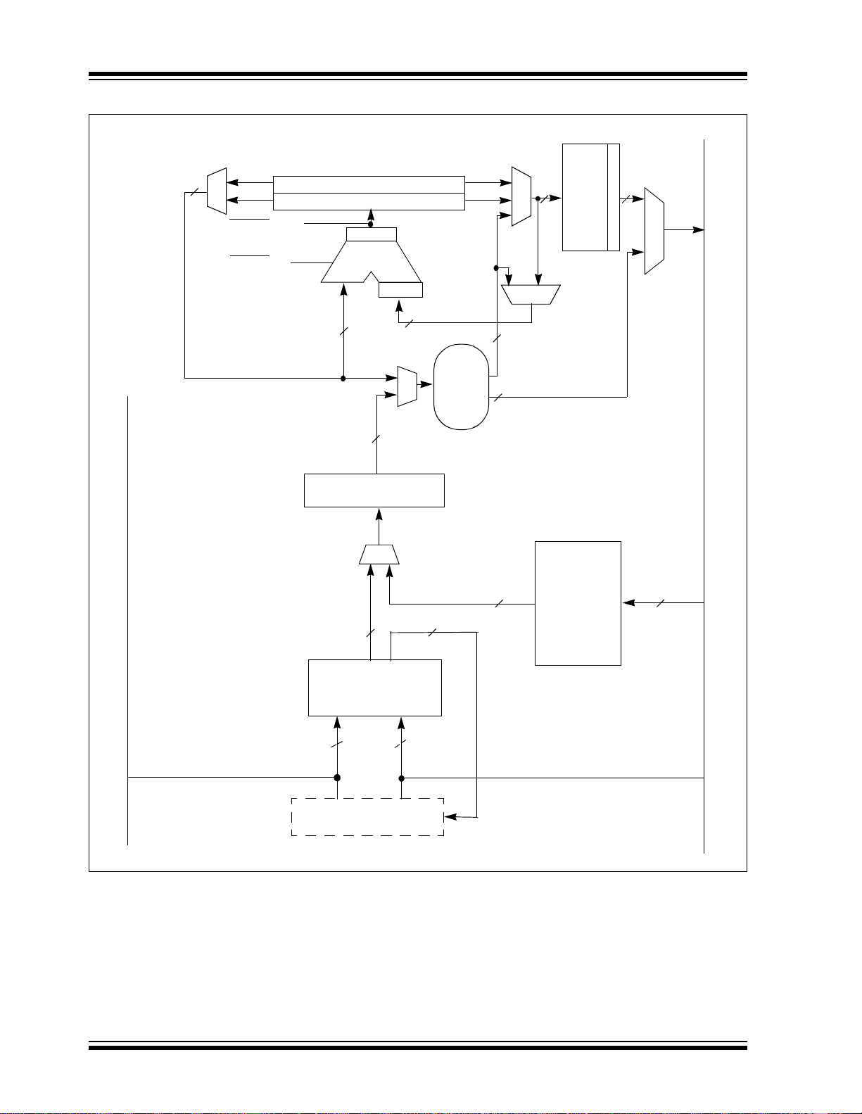
2.4 DSP Engine
The DSP engine consists of a high-speed 17-bit x
17-bit multiplier, a barrel shifter and a 40-bit adder/
subtracter (with two target accumulators, round and
saturation logic).
The DSP engine also has the capability to perform
inherent accumulator-to-accumulator operations,
which require no ad ditional dat a. These instr uctions are
ADD, SUB and NEG.
The dsPIC30F is a single-cycle instruction flow architecture, therefore, concurrent operation of the DSP
engine with MCU instruction flow is not possible.
However, some MCU ALU and DSP engine resources
may be used concu rrently by the s ame instruction (e.g.,
ED, EDAC). See Table 2-2.
TABLE 2-2: DSP INSTRUCTION SUMMARY
Instruction Algebraic Operation ACC WB?
CLR A = 0 Yes
ED A = (x – y)
EDAC A = A + (x – y)
MAC A = A + (x * y) Yes
MAC A = A + x
MOVSAC No change in A Yes
MPY A = x * y No
MPY.N A = – x * y No
MSC A = A – x * y Yes
The DSP engine has various options selected through
various bits in the CPU Core Configuration register
(CORCON), as listed below:
1. Fractional or integer DSP multiply (IF).
2. Signed or unsigned DSP multiply (US).
3. Conventional or convergent rounding (RND).
4. Automatic saturation on/off for ACCA (SATA).
5. Automatic saturation on/off for ACCB (SATB).
6. Automatic saturation on/off for writes to data
memory (SATDW).
7. Accumulator Saturation mode selection
(ACCSAT).
Note: For CORCON layout, see Table 3-3.
A block diagram of the DSP engine is shown in
Figure 2-2.
2
2
2
No
No
No
© 2006 Microchip Technology Inc. DS70139E-page 21
dsPIC30F2011/2012/3012/3013
FIGURE 2-2: DSP ENGINE BLOCK DIAGRAM
40
Carry/Borrow Out
Carry/Borrow In
40-bit Accumulator A
40-bit Accumulator B
Saturate
Adder
Negate
40
Round
Logic
S
a
16
t
u
r
a
t
e
Y Data Bus
40
40
Sign-Extend
33
17-bit
Multiplier/Scaler
16
16
40
Barrel
Shifter
32
32
40
16
X Data Bus
16
Zero Backfill
To/From W Array
DS70139E-page 22 © 2006 Microchip Technology Inc.

dsPIC30F2011/2012/3012/3013
2.4.1 MULTIPLIER
The 17 x 17-bit multiplier is capable of signed or
unsigned operati on and can mul tiplex i ts ou tput usi ng a
scaler to support either 1.31 fractional (Q31) or 32-bit
integer results. Unsigned operands are zero-extended
into the 17th bit of the multiplier input value. Signed
operands are sign-exten ded into the 17th bit of the mu ltiplier input value. The output of the 17 x 17-bit multiplier/scaler is a 33-bit value which is sign-extended to
40 bits. Integer data is inherently represented as a
signed two’s complement value, where the MSB is
defined as a sign bit. Generally speaking, the range of
an N-bit two’s compleme nt in teger i s -2
For a 16-bit integer, the data range is -32768 (0x8000)
to 32767 (0x7FFF) including ‘0’. For a 32-bit integer,
the data range is -2,147,483,648 (0x8000 0000) to
2,147,483,645 (0x7FFF FFFF).
When the multiplier is configured for fractional multiplication, the data is represented as a two’s complement
fraction, where the M SB is defined as a sign b it and the
radix point is impl ied to lie just after the sign b it (QX format). The range of an N-bit two’s complement fraction
with this implied radix point is -1.0 to (1 – 2
16-bit fraction, the Q15 data range is -1.0 (0x8000) to
0.999969482 (0x7FFF) including ‘0’ and has a precision of 3.01518x10
multiply operation genera tes a 1.3 1 produ ct, whi ch ha s
a precision of 4.65661 x 10
The same multiplier is used to support the MCU multiply instructions, which include integer 16-bit signed,
unsigned and mixed sign multiplies.
The MUL instruction can be directed to use byte or
word-sized operands. Byte operands direct a 16-bit
result. Word op erands direct a 32-bi t result to the s pecified register(s) in the W array.
-5
. In Fractional mode, the 16x16
-10
.
N-1
to 2
1-N
N-1
– 1.
). For a
2.4.2 DATA ACCUMULATORS AND ADDER/SUBTRACTER
The data accumulator consists of a 40-bit adder/
subtracter with automatic sign extension logic. It can
select one of two accumulators (A or B) as its preaccumulation source and post-accumulation destination. For the ADD and LAC instructions, the data to be
accumulated or load ed ca n be optio nally sca led v ia th e
barrel shifter prior to accumulation.
2.4.2.1 Adder/Subtracter, Overflow and
Saturation
The adder/subtracter is a 40-bit adder with an optional
zero input into one side and either true or complement
data into the other input. In the case of addition, the
carry/borrow
true data (not complemented), whereas in the case of
subtraction, the carry/bo rrow
other input is complemented. The adder/subtracter
generates overflow Status bits SA/SB and OA/OB,
which are latched and refle cted in the ST A T US register:
• Overflow from bit 39: this is a catastrophic
overflow in which the sign of the accumulator is
destroyed.
• Overflow into guard bits 32 through 39: this is a
recoverable overflow. This bit is set whenever all
the guard bits are not identical to each other.
The adder has an additional saturation block which
controls accumulat or data satu ration if selected . It uses
the result of the adder, the overflow Status bits
described above, and the SATA/B (CORCON<7:6>)
and ACCSAT (CORCON<4>) mode control bits to
determine when and to what value to saturate.
Six STATUS register bits have been provided to
support saturation and overflow. They are:
1. OA:
ACCA overflowed into guard bits
2. OB:
ACCB overflowed into guard bits
3. SA:
ACCA saturated (bit 31 overflow and sa turation)
or
ACCA overflowed into guard bits and saturated
(bit 39 overflow and s aturation)
4. SB:
ACCB saturated (bit 31 overflow and sa turation)
or
ACCB overflowed into guard bits and saturated
(bit 39 overflow and s aturation)
5. OAB:
Logical OR of OA and OB
6. SAB:
Logical OR of SA and SB
The OA and OB bits are modified each time data
passes through the adder/subtracter. When set, they
indicate that the most recent operation has overflowed
into the accumulator guard bits (bits 32 through 39).
The OA and OB bits can also optionally generate an
arithmetic warning trap when set and the corresponding overflow trap flag enable bit (OVATE, OVBTE) in
the INTCON1 register (refer to Section 8.0 “Inter-
rupts”) is set. This allows the user to take immediate
action, for example, to correct system gain.
input is active high and the other input is
input is active low and the
© 2006 Microchip Technology Inc. DS70139E-page 23

dsPIC30F2011/2012/3012/3013
The SA and SB bits are modified each time data
passes through the adder/subtracter but can only be
cleared by the user. When set, th ey indicate th at the
accumulator has overfl owed it s m aximum range (b it 31
for 32-bit saturation or bit 39 for 40-bit saturation) and
will be saturated if saturation is enabled. When saturation is not enabled, SA and SB default to bit 39 overflow
and thus indicate that a catastrophic overflow has
occurred. If the COVT E bit in th e INTCO N1 regi ster is
set, SA and SB bits ge nerate an arithmet ic warning trap
when saturation is disabled.
The overflow and saturation Status bits can optionally
be viewed in the STATUS register (SR) as the lo gical
OR of OA and OB (in bit OAB) and the logical OR of SA
and SB (in bit SAB). This allows programmers to check
one bit in the STATUS register to determine if either
accumulator has overflowed, or one bit to determine if
either accumulator has s aturated. T his w ould be us eful
for complex number arithmetic which typically uses
both the accumulators.
The device supports three saturation and overflow
modes:
1. Bit 39 Overflow and Saturation:
When bit 39 overflow and saturation occurs, the
saturation logic loads the maximally positive 9.31
(0x7FFFFFFFFF) or maximally negative 9.31
value (0x8000000000) into the target accumulator. The SA or SB bit is set and remains set until
cleared by the user. This is referred to as ‘super
saturation’ and provides protection against erroneous data or unexpected algorithm problems
(e.g., gain calculations).
2. Bit 31 Overflow and Saturation:
When bit 31 overflow and saturation occurs, the
saturation logic then loads the maximally positive 1.31 value (0x007FFFFFFF) or maximally
negative 1.31 value (0x0080000000) into the
target accumulator. The SA or SB bit is set and
remains set until cleared by the user. When this
Saturation mode is in effect, the guard bits are
not used, so the OA, OB or OAB bits are never
set.
3. Bit 39 Catastrophic Overflow:
The bit 39 overflow Status bit from the adder is
used to set the SA or SB bit which remains set
until cleared by the user. No saturation operation
is performed and the accumulator is allowed to
overflow (destroying it s sign). If the C OVTE bit in
the INTCON1 register is set, a catastrophic
overflow can initiate a trap exception.
2.4.2.2 Accumulator ‘Write-Back’
The MAC class of instructions (with the exception of
MPY, MPY.N, ED and EDAC) can optionally write a
rounded version of the high word (bits 31 through 16)
of the accumulator that is not targeted by the instructio n
into data spac e memory. The write is performed across
the X bus into combined X and Y address space. The
following addressing modes are supported:
1. W13, Register Direct:
The rounded contents of the non-target
accumulator are written into W13 as a 1.15
fraction.
2. [W13]+=2, Register Indirect with Post-Increment:
The rounded conten ts of the non- target accumulator are written into the address pointed to by
W13 as a 1.15 fraction. W13 is then
incremented by 2 (for a word write).
2.4.2.3 Round Logic
The round logic is a combinational block which performs a conventional (biased) or convergent (unbiased) round function during an accumulator write
(store). The Round mode is determined by the state of
the RND bit in the CORCON register . It generates a 16bit, 1.15 data value, which is passed to the data space
write saturation logic. If rounding is no t indicated by the
instruction, a truncated 1.15 data value is stored and
the least significant word (lsw) is simply discarded.
Conventional rounding takes bit 15 of the accumulator,
zero-extends it and ad ds it to the AC CxH w ord (bi t s 16
through 31 of the accumulator). If the ACCxL word
(bits 0 through 15 of the accumulator) is between
0x8000 and 0xFFFF (0x8000 included), ACCxH is
incremented. If ACCx L is between 0x000 0 and 0x7FFF,
ACCxH is left unchanged. A conse que nc e of thi s alg orithm is that over a succession of random rounding
operations, the value tends to be biased slightly
positive.
Convergent (or unbiased) rounding operates in the
same manner as conventional rounding, except when
ACCxL equals 0x8000. If this is the case, the LSb
(bit 16 of the accumulator) of ACCxH is examined. If it
is ‘1’, ACCxH is incremented. If it is ‘0’, ACCxH is not
modified. As sumi ng t hat bi t 16 is effe cti vely r and om in
nature, this scheme w i ll re mo ve any rou ndi ng b ias th at
may accumulate.
The SAC and SAC.R instructions store either a truncated (SAC) or rounded (SAC.R) version of the c ontents
of the target ac cumu la tor to d ata memo ry via th e X bu s
(subject to data saturation, see Section 2.4.2.4 “Data
Space Write Saturation”). Note that for the MAC cl as s
of instructions, the accumulator write-back operation
functions in the same manner, addressing combined
MCU (X and Y) data space though the X bus. For this
class of instructions, the data is always subject to
rounding.
DS70139E-page 24 © 2006 Microchip Technology Inc.

dsPIC30F2011/2012/3012/3013
2.4.2.4 Data Space Write Saturation
In addition to adder/subtrac ter saturation, writes to dat a
space may also be saturated but without affecting the
contents of the source accumulator. The data space
write saturation logic block accepts a 16-bit, 1.15 fractional value from the round logic block as its input,
together with overflow status from the original source
(accumulator) and the 16-bit round adder. These are
combined and used to select the appropriate 1.15
fractional value as output to write to data space
memory.
If the SATDW bit in the CORCON register is set, data
(after rounding or truncation) is tes te d for ove rflo w and
adjusted accordingly. For input data greater than
0x007FFF, data written to memory is force d to the maximum positi ve 1. 15 val ue, 0x 7FFF. For input data less
than 0xFF8000, da ta wr itten to me mory i s forced to th e
maximum negative 1.1 5 value, 0x8000. The MSb of the
source (bit 39) is used to determine the sign of the
operand being tested.
If the SA TDW bi t in the CORCON regis ter is not set , the
input data is always passed through unmodified under
all conditions.
2.4.3 BARREL SHIFTER
The barrel shifter is capable of performing up to 16-bit
arithmetic or logic right shifts, or up to 16-bit left shifts
in a single c ycle. The sou rce can be ei ther of th e two
DSP accumul ators, or the X bus (t o support multi-bit
shifts of register or memory data).
The shifter requi res a signed binary val ue to de term in e
both the magnitude (num ber of bits) and direction of the
shift operation. A po sitive value shift s the operand right.
A negative value shifts the operand left. A value of ‘0’
does not modify the operand.
The barrel shifter is 40 bits wide, thereby obtaining a
40-bit result for DSP shift operati ons and a 16- bit result
for MCU shift operations. Data from the X bus is presented to the barrel shifter between bit positions 16 to
31 for right shift s, and bit pos itions 0 to 16 for left shift s.
© 2006 Microchip Technology Inc. DS70139E-page 25

dsPIC30F2011/2012/3012/3013
NOTES:
DS70139E-page 26 © 2006 Microchip Technology Inc.

dsPIC30F2011/2012/3012/3013
3.0 MEMORY ORGANIZATION
Note: This data sheet summarizes features of this group
of dsPIC30F devices and is not intended to be a complete
reference source. For more information on the CPU,
peripherals, register descriptions and general device
functionality, refer to the “dsPIC30F Family Reference
Manual” (DS70046). For more informat ion on the device
instruction set and programming, refer to the “dsPIC30F/
33F Programmer’s Reference Manual “ (DS70157).
3.1 Program Address Space
The program address space is 4M instruction words.
The program sp ace mem ory map fo r the dsPI30 F2011/
2012 is shown in Figure 3-1. The program space
memory map for the dsPI30F3012/3013 is shown in
Figure 3-2.
Program memory is addres sable by a 24 -bit value from
either the 23-bit PC, table instruction Effective Address
(EA), or data space EA, when program space is
mapped into data space as defined by Table 3-1. Note
that the program space address is incremented by two
between successiv e progr am w ords in o rder to prov ide
compatibility with data space addressing.
User program space access is restricted to the lower
4M instruction word address range (0x000000 to
0x7FFFFE) for all accesses other than TBLRD/TBLWT,
which uses TBLPAG<7> to determine user or configuration space access. In Table 3-1, Program Space
Address Construction, bit 23 allows access to the
Device ID, the User ID and the Configuration bits.
Otherwise, bit 23 is always clear.
© 2006 Microchip Technology Inc. DS70139E-page 27
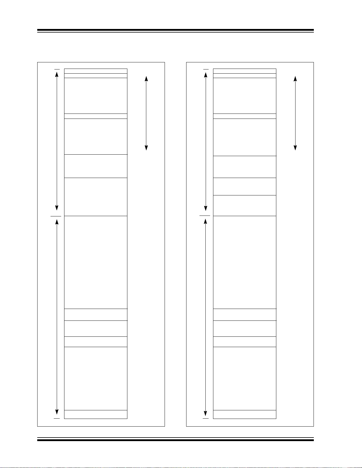
dsPIC30F2011/2012/3012/3013
FIGURE 3-1: dsPIC30F2011/2012
PROGRAM SPACE
MEMORY MAP
Reset - GOTO Instruction
Reset - Target Address
Interrupt Vector Table
Reserved
Alternate Vector Table
Space
User Memory
User Flash
Program Memory
(4K instructions)
Reserved
(Read ‘0’s)
000000
000002
000004
Vector Tables
00007E
000080
000084
0000FE
000100
001FFE
002000
7FFFFE
800000
FIGURE 3-2: dsPIC30F3012/3013
PROGRAM SPACE
MEMORY MAP
Reset - GOTO Instruction
Reset - Target Address
Interrupt Vector Table
Reserved
Alternate Vector Table
Space
User Memory
User Flash
Program Memory
(8K instructions)
Reserved
(Read ‘0’s)
Data EEPROM
(1 Kbyte)
000000
000002
000004
Vector Tables
00007E
000080
000084
0000FE
000100
003FFE
004000
7FFBFE
7FFC00
7FFFFE
800000
Reserved
8005BE
Space
Configuration Memory
UNITID (32 instr.)
Reserved
Device Configuration
Registers
Reserved
DEVID (2)
8005C0
8005FE
800600
F7FFFE
F80000
F8000E
F80010
FEFFFE
FF0000
FFFFFE
Space
Configuration Memory
Reserved
UNITID (32 instr.)
Reserved
Device Configuration
Registers
Reserved
DEVID (2)
8005BE
8005C0
8005FE
800600
F7FFFE
F80000
F8000E
F80010
FEFFFE
FF0000
FFFFFE
DS70139E-page 28 © 2006 Microchip Technology Inc.

dsPIC30F2011/2012/3012/3013
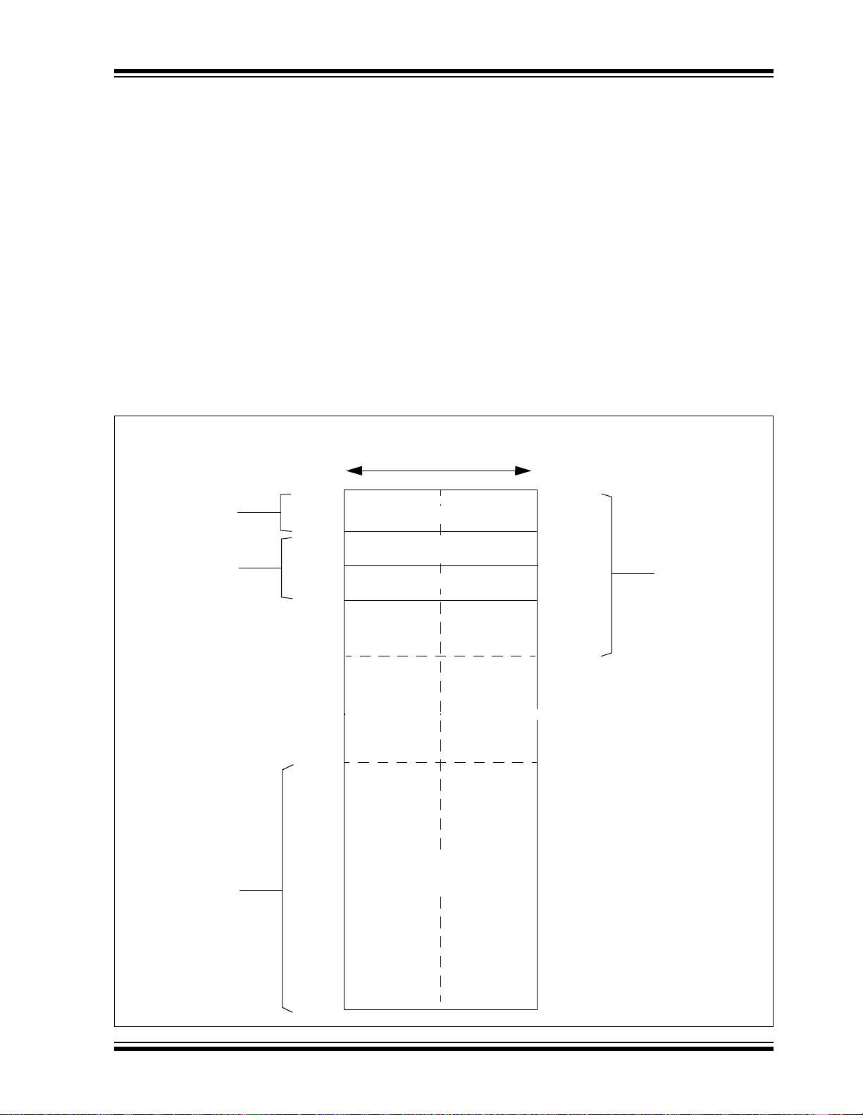
TABLE 3-1: PROGRAM SPACE ADDRESS CONSTRUCTION
Access Type
Instruction Access User 0 PC<22:1> 0
TBLRD/TBLWT User
TBLRD/TBLWT Configuration
Program Space Visibility User 0 PSVPAG<7:0> Data EA<14:0>
Access
Space
(TBLPAG<7> = 0)
(TBLPAG<7> = 1)
<23> <22:16> <15> <14:1> <0>
TBLPAG<7:0> Data EA<15:0>
TBLPAG<7:0> Data EA<15:0>
FIGURE 3-3: DATA ACCESS FROM PROGRAM SPACE ADDRESS GENERATION
23 bits
Using
Program
Counter
0
Program Space Address
0Program Counter
Select
Using
Program
Space
Visibility
Using
Table
Instruction
User/
Configuration
Space
Select
Note: Program space visibility cannot be used to access bits <23:16> of a word in program memory.
0
PSVPAG Reg
1/0
TBLPAG Reg
8 bits
8 bits
1
24-bit EA
EA
15 bits
EA
16 bits
Byte
Select
© 2006 Microchip Technology Inc. DS70139E-page 29

dsPIC30F2011/2012/3012/3013
3.1.1 DATA ACCESS FROM PROGRAM MEMORY USING TABLE INSTRUCTIONS
This architecture fetc hes 24 -bi t w ide pro gram m emo ry.
Consequently, instructions are always aligned.
However, as the architecture is modified Harvard, data
can also be present in program space.
There are two methods by which program space can
be accessed: via special table instructions, or through
the remapping of a 16 K word program space p age in to
the upper half o f da ta space (see Section 3.1.2 “Data
Access from Program Memory Using Program
Space Visibility”). The TBLRDL and TBLWTL instruc-
tions offer a direct method of reading or writing the lsw
of any address within program space, without going
through data sp ac e. The TBLRDH and TBLWTH instruc-
tions are the only method wh ereby the upp er 8 bits of a
program space word can be accessed as data.
The PC is incremented by two for each successive
24-bit program word. This allows program memory
addresses to directly map to data space addresses.
Program memory can thus be regarded as two 16-bit
word wide address sp ac es , res id ing si de by si de, each
with the same address range. TBLRDL and TBLWTL
access the space whic h co n tai ns the ls w, and TBLRDH
and TBLWTH access the space which contains the
MSB.
Figure 3-3 shows h ow th e EA is created for table op erations and data space accesses (PSV = 1). Here,
P<23:0> refers to a program space word, whereas
D<15:0> refers to a data space word.
A set of table in st ruc tion s a re p r ov ide d t o m ov e by te or
word-sized data to and from program space. See Figure 3-4 and Figure 3-5.
1. TBLRDL: Table Read Low
Word: Read the LS Word of the pr ogram add ress;
P<15:0> maps to D<15:0>.
Byte: Read one of the LSB of the program
address;
P<7:0> maps to the destination byte when byte
select = 0;
P<15:8> maps to the d estination b yte when byte
select = 1.
2. TBLWTL: Table Write Low (ref er to Section 5.0
“Flash Program Memory” for details on Flash
Programming)
3. TBLRDH: Table Read Hi gh
Word: Read the MS Word of the program address;
P<23:16> maps to D<7 :0> ; D<15 :8> will al way s
be = 0.
Byte: Read one of the MSB of the program
address;
P<23:16> maps to the destination byte when
byte select = 0;
The destination byte will always be = 0 when
byte select = 1.
4. TBLWTH: Table Write High (refer to Section 5.0
“Flash Program Memory” for details on Flash
Programming)
FIGURE 3-4: PROGRAM DATA TABLE ACCESS (lsw)
PC Address
0x000000
0x000002
0x000004
0x000006
Program Memory
‘Phantom’ Byte
(read as ‘0’)
00000000
00000000
00000000
00000000
23
TBLRDL.W
16
8
TBLRDL.B (Wn<0> = 0)
TBLRDL.B (Wn<0> = 1)
0
DS70139E-page 30 © 2006 Microchip Technology Inc.

dsPIC30F2011/2012/3012/3013
FIGURE 3-5: PROGRAM DATA TABLE ACCESS (MSB)
TBLRDH.W
PC Address
0x000000
0x000002
0x000004
0x000006
Program Memory
‘Phantom’ Byte
(read as ‘0’)
00000000
00000000
00000000
00000000
23
TBLRDH.B (Wn<0> = 1)
3.1.2 DATA ACCESS FROM PROGRAM MEMORY USING PROGRAM SPACE VISIBILITY
The upper 32 Kbytes of data space may optionally be
mapped into any 16K word program space page. This
provides transparent access of stored constant data
from X data space without the need to use special
instructions (i.e., TBLRDL/H, TBLWTL/H instru cti ons).
Program space access through the data space occurs
if the MSb of the data space EA is set and program
space visibility is enabled by setting the PSV bit in the
Core Control register (CORCON). The functions of
CORCON are discussed in Section 2.4 “DSP
Engine”.
Data accesses to this area add an additional cycle to
the instruction being executed, since two program
memory fetches are required.
Note that the upper half of addressable data space is
always part of the X data space. Therefore, when a
DSP operation uses program sp ace mapp ing to acc ess
this memory region , Y d ata space sho uld ty pic al ly co ntain state (variable) data for DSP operations, whereas
X data space should typically contain coefficient
(constant) data.
Although each da ta sp ace addres s, 0x8000 and higher ,
maps directly into a corresponding program memory
address (see Figure 3-6), only the lower 16 bits of the
24-bit program word are used to contain the data. The
upper 8 bits shoul d be progra mmed to forc e an illeg al
instruction to maintain machine robustness. Refer to
the “dsPIC30F/33F Programmer’s Reference Manual”
(DS70157) for details on instruction encoding.
16
TBLRDH.B (Wn<0> = 0)
Note that by incrementing the PC by 2 for each
program memory word, the LS 15 bits of data space
addresses directly map to the LS 15 bits in the corresponding program space addresses. The remaining
bits are provided by the Program Space Visibility Page
register, PSVPAG<7:0>, as shown in Figure3-6.
Note: PSV access is temporarily disabled during
table reads/writes.
For instructions that use PSV which are executed
outside a REPEAT loop:
• The following instructions require one instruction
cycle in addition to the specified execution time:
- MAC class of instructions with data operand
prefetch
- MOV instructions
- MOV.D instructions
• All other instructio ns require two i nstruction cyc les
in addition to the specified execution time of the
instruction.
For instructions that use PSV which are executed
inside a REPEAT loop:
• The following instances require two instruction
cycles in addition to the specified execution time
of the instruction:
- Execution in the first iteration
- Execution in the last iteration
- Execution prior to exiting the loop due to an
interrupt
- Execution upon re-entering the loop after an
interrupt is serviced
• Any other iteration of the REPEAT loop allow the
instruction accessi ng da t a, usin g PSV, to execute
in a single cycle.
8
0
© 2006 Microchip Technology Inc. DS70139E-page 31

dsPIC30F2011/2012/3012/3013
FIGURE 3-6: DATA SPACE WINDOW INTO PROGRAM SP ACE OPERATION
Data Space
0x0000
EA<15> =
16
Data
Space
EA
EA<15> = 1
Upper Half of Data
Space is Mapped
into Program Space
BSET CORCON,#2 ; Set PSV bit
MOV #0x0, W0 ; Set PSVPAG register
MOV W0, PSVPAG
MOV 0x9200, W0 ; Access program memory location
15
0
15
; using a data space access
0x8000
15
0xFFFF
PSVPAG
Address
Concatenation
0x00
Program Space
0x000000
(1)
8
23 15 0
23
Data Read
0x001200
0x001FFF
Note 1: PSVPAG is an 8-bit register, containing bits <22:15> of the program space address.
DS70139E-page 32 © 2006 Microchip Technology Inc.
dsPIC30F2011/2012/3012/3013
3.2 Data Address Space
The core has two data spaces. The data spaces can be
considered either separate (for some DSP instructions), or as one unified linear address range (fo r MCU
instructions). The dat a spaces are accessed using tw o
Address Generation Units (AGUs) and separate data
paths.
3.2.1 DATA SPACE MEMORY MAP
The data space memory is split into two blocks, X and
Y data space. A key element of this architectur e is th at
Y space is a subset of X space, and is fully contained
within X space. In order to provide an apparent Linear
Addressing space, X and Y spaces have contiguous
addresses.
When executing any instruction other than one of the
MAC class of instructio ns, the X block cons ists of the 6 4Kbyte data address space (including all Y addresses).
When executing one of the MAC class of instructions,
the X block consists of the 64-Kbyte data address
space, excluding the Y address block (for data reads
only). In other words, all other instructions regard the
entire data memory as one composite address space.
The MAC class instructions extract the Y address space
from data space and address it using EAs sourced from
W10 and W11. The remaining X data space is
addressed using W8 an d W9. Both addres s spaces a re
concurrently accessed only with the MAC class
instructions.
The data space memory map for the dsPIC30F2011
and dsPIC30F2012 is shown in Figure 3-7. The data
space memory map for the dsPIC30F3012 and
dsPIC30F3013 is shown in Figure 3-8.
FIGURE 3-7: dsPIC30F2011/2012 DATA SPACE MEMORY MAP
2 Kbyte
SFR Space
1 Kbyte
SRAM Space
MSB
Address
0x0001
0x07FF
0x0801
0x09FF
0x0A01
0x0BFF 0x0BFE
16 bits
SFR Space
X Data RAM (X)
Y Data RAM (Y)
LSBMSB
0x0000
0x07FE
0x0800
0x09FE
0x0A00
0x0C000x0C01
LSB
Address
8 Kbyte
Near
Data
Space
Optionally
Mapped
into Program
Memory
0x8001
0xFFFF
0x1FFE 0x1FFF
0x8000
X Data
Unimplemented (X)
0xFFFE
© 2006 Microchip Technology Inc. DS70139E-page 33

dsPIC30F2011/2012/3012/3013
FIGURE 3-8: dsPIC30F3012/3013 DATA SPACE MEMORY MAP
2 Kbyte
SFR Space
2 Kbyte
SRAM Space
MSB
Address
0x0001
0x07FF
0x0801
0x0BFF
0x0C01
0x0FFF 0x0FFE
0x8001
16 bits
LSBMSB
SFR Space
X Data RAM (X)
Y Data RAM (Y)
Address
0x0000
0x07FE
0x0800
0x0BFE
0x0C00
0x10000x1001
0x1FFE 0x1FFF
0x8000
LSB
8 Kbyte
Near
Data
Space
Optionally
Mapped
into Program
Memory
0xFFFF
X Data
Unimplemented (X)
0xFFFE
DS70139E-page 34 © 2006 Microchip Technology Inc.

dsPIC30F2011/2012/3012/3013
FIGURE 3-9: DATA SPACE FOR MCU AND DSP (MAC CLASS) INSTRUCTIONS EXAMPLE
SFR SPACE
UNUSED
(Y SPACE)
X SPACE
Non-MAC Class Ops (Read/Write) MAC Clas s Ops (Read)
MAC Class Ops (Write)
Indirect EA using any W Indirect EA using W8, W9 Indirect EA using W10, W11
Y SPACE
UNUSED
SFR SPACE
UNUSED
X SPACE
X SPACE
© 2006 Microchip Technology Inc. DS70139E-page 35

dsPIC30F2011/2012/3012/3013
3.2.2 DATA SPACES
The X data space is used by all instructions and supports all addressing modes. There are separate read
and write data buses. The X read data bus is the return
data path for all inst ructions that view data spac e as
combined X and Y address space. It is also the X
address space data path for the dual operand read
instructions (MAC class). The X write data bus is the
only write path to data space for all instructions.
The X data space also supp orts Mod ulo Addressin g for
all instructions, subject to Addressing mode restrictions. Bit-Reversed Addressing is only supported for
writes to X data space.
The Y data space is used in concert with the X data
space by the MAC class of instructions (CLR, ED,
EDAC, MAC, MOVSAC, MPY, MPY.N and MSC) to
provide two concurrent data read paths. No writes
occur across the Y bus. T his cl as s of ins t ruct io ns ded icates two W register pointers , W10 and W1 1, to always
address Y data space, independent of X data space,
whereas W8 and W9 always address X data space.
Note that during accumulator write back, the data
address space is con si dere d a c om bin ati on of X and Y
data spaces, so the write occurs across the X bus.
Consequently, the write can be to any address in the
entire data space.
The Y data space can only be used for the data
prefetch operation associated with the MAC class of
instructions. It also supports Modulo Addressing for
automated circular bu f fe rs. O f c ours e, all othe r ins tru ctions can access the Y dat a address sp ace through the
X data path as part of the composite linear space.
The boundary between the X and Y data spaces is
defined as shown in Figure 3-8 and is not user programmable. Shoul d an EA poin t to d ata out side it s own
assigned address space, or to a location outside physical memory, an all zero word/byte is returned. For
example, although Y address space is visible by all
non-MAC instructions using any addressing mode, an
attempt by a MAC instruction to fetch data from that
space using W8 or W9 (X space pointers) returns
0x0000.
TABLE 3-2: EFFECT OF INVALID
MEMORY ACCESSES
Attempted Operation Data Returned
EA = an unimplemented address 0x0000
W8 or W9 used to access Y data
space in a MAC instruction
W10 or W11 used to access X
data space in a MAC instruction
0x0000
0x0000
3.2.3 DATA SPACE WIDTH
The core data width is 16 bits. All internal registers are
organized as 16-bit wide words. Data space memory is
organized in byte addressable, 16-bit wide blocks.
3.2.4 DATA ALIGNMENT
To help maintain backward compatibility with PIC
MCU devices and improve data space memory usage
efficiency, the dsPIC30F instruction set supports both
word and byte operation s. Data i s aligned in dat a memory and registers as words, but all data space EAs
resolve to bytes. Data byte reads read the complete
word that contai ns the byte, us ing the LSb of any EA to
determine which byte to select. The selected byte is
placed onto the LSB of the X data path (no byte
accesses are possible fro m the Y data pa th as the MAC
class of instruction can only fetch words). That is, data
memory and registers are organized as two parallel
byte wide entities with shared (word) address decode
but separate write lines. Data byte writes only write to
the corresponding side of the array or register which
matches the byte address.
As a consequence of t his byte accessib ility , all Ef fective
Address calculations (includin g those generate d by the
DSP operations which are restricted to word-sized
data) are internal ly scaled to ste p through word-ali gned
memory. For example, the core would recognize that
Post-Modified Register Indirect Addressing mode
[Ws++] results in a value of Ws + 1 for byte operations
and Ws + 2 for word operations.
All word accesses m ust be al igned to an even addre ss.
Misaligned word data fetches are not supported so
care must be taken when mixing byte and word operations, or translatin g from 8-bit MCU cod e. Should a misaligned read or write be attempted, an address error
trap is generated. If the error occurred on a read, the
instruction underway is completed, whereas if it
occurred on a write, the instruction is executed, but the
write does not occur. In either case, a trap is then executed, allowing the system and/or user to examine the
machine state prior to execution of the address fault.
FIGURE 3-10: DATA ALIGNMENT
15 8 7 0
0001
0003
0005
Byte 1 Byte 0
Byte 3 Byte 2
Byte 5 Byte 4
LSBMSB
0000
0002
0004
®
All Effective Addresses are 16 bits wide and point to
bytes within the data space. Therefore, the data space
address range is 64 Kbytes or 32K words.
DS70139E-page 36 © 2006 Microchip Technology Inc.

dsPIC30F2011/2012/3012/3013
All byte loads into any W register are loaded into the
LSB. The MSB is not modified.
A Sign-Extend (SE) instruction is provided to allow
users to translate 8-bit signed data to 16-bit signed
values. Alternatively, for 16-bit unsigned data, users
can clear the MSB of any W register by executing a
Zero-Extend (ZE) instruction on the appropriate
address.
Although most ins truc tio ns a r e ca p ab le of operating on
word or byte data sizes, it should be noted that some
instructions, including the DSP instructions, operate
only on words.
3.2.5 NEAR DATA SPACE
An 8-Kbyte ‘near’ data space is reserved in X address
memory space between 0x0000 and 0x1FFF, which is
directly addressable via a 13- bit absolute address fiel d
within all memory direct instructions. The remaining X
address space and all of the Y address space is
addressable indirec tly. Additionally, the who le of X dat a
space is addressable using MOV instructions, which
support memory direct addressing with a 16-bit
address field.
3.2.6 SOFTWARE STACK
There is a Stack Pointer Limit register (SPLIM) associated with the Stack Pointer. SPLIM is uninitialized at
Reset. As is t he case f or t h e Stack Point er, SPLIM<0>
is forced to ‘0’ because all stack operations must be
word aligned. Whenever an Effective Address (EA) is
generated using W15 as a source or destination
pointer, the address thus generated is compared with
the value in SPLIM. If the contents of the Stack Pointer
(W15) and the SPLIM register are equal, and a push
operation is performed, a stack error trap does not
occur. The stack error trap occurs on a subsequent
push operation. Thus, for example, if it is desirable to
cause a stack error trap when the stack grows beyond
address 0x2000 in RAM, initialize the SPLIM with the
value, 0x1FFE.
Similarly, a Stack Pointer un derflow ( sta ck erro r) trap is
generated when the Stack Pointer address is found to
be less than 0x0800, thus preventing the stack from
interfering with the Special Function Register (SFR)
space.
A write to the SPLIM regis ter should not be im mediately
followed by an indirect read operati on usi ng W15.
The dsPIC DSC de vices contai n a softw are st ack. W1 5
is used as the Stack Pointer.
The Stack Pointer always points to the first available
free word and grows from lower addresses towards
higher addresses. It pre-decrements for stack pops
and post-increments for stack pushes, as shown in
Figure 3-11. Note that for a PC push during any CALL
instruction, the M SB o f t he PC i s ze ro-extended before
the push, ensuring that the MSB is always clear.
Note: A PC push during exception processing
concatenates the SRL regis ter to th e MSB
of the PC prior to the push.
FIGURE 3-11: CALL STACK FRAME
0x0000
Stack Grows Towards
000000000
Higher Address
PC<15:0>
PC<22:16>
<Free Word>
015
W15 (before CALL)
W15 (after CALL)
POP : [--W15]
PUSH : [W15++]
© 2006 Microchip Technology Inc. DS70139E-page 37
DS70139E-page 38 © 2006 Microchip Technology Inc.
TABLE 3-3: CORE REGISTER MAP
SFR Name
W0 0000 W0/WREG 0000 0000 0000 0000
W1 0002 W1 0000 0000 0000 0000
W2 0004 W2 0000 0000 0000 0000
W3 0006 W3 0000 0000 0000 0000
W4 0008 W4 0000 0000 0000 0000
W5 000A W5 0000 0000 0000 0000
W6 000C W6 0000 0000 0000 0000
W7 000E W7 0000 0000 0000 0000
W8 0010 W8 0000 0000 0000 0000
W9 0012 W9 0000 0000 0000 0000
W10 0014 W10 0000 0000 0000 0000
W11 0016 W11 0000 0000 0000 0000
W12 0018 W12 0000 0000 0000 0000
W13 001A W13 0000 0000 0000 0000
W14 001C W14 0000 0000 0000 0000
W15 001E W15 0000 1000 0000 0000
SPLIM 0020 SPLIM 0000 0000 0000 0000
ACCAL 0022 ACCAL 0000 0000 0000 0000
ACCAH 0024 ACCAH 0000 0000 0000 0000
ACCAU 0026 Sign Extension (ACCA<39>) ACCAU 0000 0000 0000 0000
ACCBL 0028 ACCBL 0000 0000 0000 0000
ACCBH 002A ACCBH 0000 0000 0000 0000
ACCBU 002C Sign Extension (ACCB<39>) ACCBU 0000 0000 0000 0000
PCL 002E PCL 0000 0000 0000 0000
PCH 0030
TBLPAG 0032
PSVPAG 0034
RCOUNT 0036 RCOUNT uuuu uuuu uuuu uuuu
DCOUNT 0038 DCOUNT uuuu uuuu uuuu uuuu
DOSTARTL 003A DOSTARTL 0 uuuu uuuu uuuu uuu0
DOSTARTH 003C
DOENDL 003E DOENDL
DOENDH 0040
SR 0042 OA OB SA SB OAB SAB DA DC IPL2 IPL1 IPL0 RA N OV Z C 0000 0000 0000 0000
Legend: u = uninitialized bit
Note: Refer to “dsPIC30F Family Reference Manual” (DS70046) for descript ions of register bit fields.
Address
(Home)
Bit 15 Bit 14 Bit 13 Bit 12 Bit 11 Bit 10 Bit 9 Bit 8 Bit 7 Bit 6 Bit 5 Bit 4 Bit 3 Bit 2 Bit 1 Bit 0 Reset State
— — — — — — — — —PCH0000 0000 0000 0000
— — — — — — — —TBLPAG0000 0000 0000 0000
— — — — — — — — PSVPAG 0000 0000 0000 0000
— — — — — — — — —DOSTARTH0000 0000 0uuu uuuu
uuuu uuuu uuuu uuu0
0
— — — — — — — — — DOENDH 0000 0000 0uuu uuuu
dsPIC30F2011/2012/3012/3013

© 2006 Microchip Technology Inc. DS70139E-page 39
TABLE 3-3: CORE REGISTER MAP (CONTINUED)
SFR Name
CORCON 0044 — — — US EDT DL2 DL1 DL0 SATA SATB SATDW ACCSAT IPL3 PSV RND IF 0000 0000 0010 0000
MODCON 0046 XMODEN YMODEN
XMODSRT 0048 XS<15:1> 0 uuuu uuuu uuuu uuu0
XMODEND 004A XE<15:1> 1 uuuu uuuu uuuu uuu1
YMODSRT 004C YS<15:1> 0 uuuu uuuu uuuu uuu0
YMODEND 004E YE<15:1> 1 uuuu uuuu uuuu uuu1
XBREV 0050 BREN XB<14:0> uuuu uuuu uuuu uuuu
DISICNT 0052
Legend: u = uninitialized bit
Note: Refer to “dsPIC30F Family Reference Manual” (DS70046) for descript ions of register bit fields.
Address
(Home)
Bit 15 Bit 14 Bit 13 Bit 12 Bit 11 Bit 10 Bit 9 Bit 8 Bit 7 Bit 6 Bit 5 Bit 4 Bit 3 Bit 2 Bit 1 Bit 0 Reset State
— — BWM<3:0> YWM<3:0> XWM<3:0> 0000 0000 0000 0000
— — DISICNT<13:0> 0000 0000 0000 0000
dsPIC30F2011/2012/3012/3013

dsPIC30F2011/2012/3012/3013
NOTES:
DS70139E-page 40 © 2006 Microchip Technology Inc.

dsPIC30F2011/2012/3012/3013
4.0 ADDRESS GENERATOR UNITS
Note: This data sheet summarizes features of this group
of dsPIC30F devices and is not intended to be a complete
reference source. For more information on the CPU,
peripherals, register descriptions and general device
functionality, refer to the “dsPIC30F Family Reference
Manual” (DS70046). For more informat ion on the device
instruction set and programming, refer to the “dsPIC30F/
33F Programmer’s Reference Manual“ (DS70157).
The dsPIC DSC core contains two independent
address generator unit s: the X AGU an d Y AGU. The Y
AGU supports word-sized data reads for the DSP MAC
class of instructions only. The dsPIC DSC AGUs support three types of data addressing:
• Linear Addressing
• Modulo (Circular) Addressing
• Bit-Reversed Addressing
Linear and Modulo Data Addressing modes can be
applied to data space or program space. Bit-Reversed
Addressing is only applicab le to dat a s pace a ddresses .
4.1 Instruction Addressing Modes
The addressing modes in Table 4-1 form the basis of
the addressing modes optimized to support the specific
features of individual instructions. The addressing
modes provided in the MAC class of instructions are
somewhat different from those in the other instruction
types.
4.1.1 FILE REGISTER INSTRUCTIONS
Most file register ins truc tio ns use a 13-bit address field
(f) to directly address data present in the first 8192
bytes of data memory (near data space). Most file
register instructions employ a working register, W0,
which is de noted as WREG i n these instruc tions. The
destination is typically either the same file register or
WREG (with the exception of the MUL instruction),
which writes the re sult t o a re gister or regi ster p air. The
MOV instruction allows additional flexibility and can
access the entire data space during file register
operation.
4.1.2 MCU INSTRUCTIONS
The three-operand MCU instructions are of the form:
Operand 3 = Operand 1 <function> Operand 2
where Operand 1 is alw a ys a work in g reg ist er (i.e., the
addressing mode can only be register direct), which is
referred to as Wb. Operand 2 can be a W register,
fetched from data memory or a 5-bit literal. The result
location can be either a W register or an address
location. The following addressing modes are
supported by MCU instructions:
• Register Direct
• Register Indirect
• Register Indirect Post-modified
• Register Indirect Pre-modified
• 5-bit or 10-bit Literal
Note: Not all instructions support all th e address-
ing modes given above. Individual
instructions may support different subsets
of these addressing modes.
TABLE 4-1: FUNDAMENTAL ADDRESSING MODES SUPPORTED
Addressing Mode Description
File Register Direct The address of the File register is specified explicitly.
Register Direct The contents of a register are accessed directly.
Register Indirect The contents of Wn forms the EA.
Register Indirect Post-modified The contents of Wn forms the EA. Wn is post-modified (incremented or
decremented) by a constant value.
Register Indirect Pre-modified Wn is pre-modified (incremented or decremented) by a signed constant value
to form the EA.
Register Indirect with Register Offset The sum of Wn and Wb forms the EA.
Register Indirect with Literal Offset The sum of Wn and a literal forms the EA.
© 2006 Microchip Technology Inc. DS70139E-page 41

dsPIC30F2011/2012/3012/3013
4.1.3 MOVE AND ACCUMULATOR INSTRUCTIONS
Move instructions and the DSP accumulator class of
instructions provide a greater degree of addressing
flexibility than other instructions. In addition to the
addressing modes supported by most MCU instructions, move and accumulator instructions also support
Register Indirect with Register Offset Addressing
mode, also referred to as Register Indexed mode.
Note: For the MOV instructions, the addressing
mode specified in the instruction can differ
for the source and destination EA.
However, the 4-bit Wb (register offset)
field is shared between both source and
destination (but typically only used by
one).
In summary, the following addressing modes are
supported by move and accumulator instructions:
• Register Direct
• Register Indirect
• Register Indirect Post-modified
• Register Indirect Pre-modif ied
• Register Indirect with Register Offset (Indexed)
• Register Indirect with Literal Offset
• 8-bit Literal
• 16-bit Literal
Note: Not all instructions support all t he address-
ing modes given above. Individual
instructions may support different subsets
of these addressing modes.
4.1.4 MAC INSTRUCTIONS
The dual source operand DSP ins tructio ns (CLR, ED,
EDAC, MAC, MPY, MPY.N, MOVSAC and MSC), also
referred to as MAC instruct ions, utiliz e a simplified set of
addressing modes to allow the user to effectively
manipulate the data pointers through register indirect
tables.
The two source operand prefetch registers must be long
to the set {W8, W9, W10, W11}. For data reads, W8
and W9 are always directed to the X RAGU. W10 and
W11 are always directed to the Y AGU. The effective
addresses generated (before and after modification)
must, therefore, be vali d addresses withi n X data sp ace
for W8 and W9 and Y data space for W10 and W11.
Note: Register Indirect with Register Offset
addressing is only available for W9 (in X
space) and W11 (in Y space).
In summary, the following addressing modes are
supported by the MAC class of instructions:
• Register Indirect
• Register Indirect Post-modified by 2
• Register Indirect Post-modified by 4
• Register Indirect Post-modified by 6
• Register Indirect with Register Offset (Indexed)
4.1.5 OTHER INSTRUCTIONS
Besides the various addre ssing mo des outlin ed above,
some instructio ns use li teral con stant s of va rious siz es.
For example, BRA (branch) instructions use 16-bit
signed literals to spe cify the branc h destination directly,
whereas the DISI instruction uses a 14-bit unsigned
literal field. In some instructions, such as ADD Acc, the
source of an operand or result is im plied by the opcod e
itself. Cert ain opera tions, su ch as NOP, do not have any
operands.
4.2 Modulo Addressing
Modulo Addressing is a method of providing an automated means to support circular data buffers using
hardware. The objectiv e is to remo ve t he need fo r software to perform data address boundary checks when
executing tightly looped code, as is typical in many
DSP algorithms.
Modulo Addressing can operat e in either data or program space (since the data pointer mechanism is
essentially the same for b oth). One circular b uffer can
be supported in each o f the X ( which also provide s th e
pointers into progra m space) and Y d ata spaces. Modulo Addressing can operate on any W re gister pointer.
However, it is not advisable to use W14 or W15 for Modulo Addressing since these two registers are used as
the Stack Frame Pointer and Stack Pointer, respectively.
In general, any particular circular buffer can only be
configured to ope rate in one directio n, as there are certain restrictions on the buffer Start address (for incrementing buffers), or end address (for decrementing
buffers) based upon the direction of the buffer.
The only exception to the usage restrictions is for buffers that have a power -of-2 length . As these b uff ers satisfy the S tart and end address criteria, they ca n operate
in a Bidirectional mode (i.e., address boundary checks
are performed on both the lower and upper address
boundaries).
DS70139E-page 42 © 2006 Microchip Technology Inc.

dsPIC30F2011/2012/3012/3013
4.2.1 START AND END ADDRESS
The Modulo Ad dressing scheme r equires t hat a starting and an ending address be specified and loaded
into the 16-bit Modulo Buffer Address registers:
XMODSRT, XMODEND, YMODSRT and YMODEND
(see Table 3-3).
Note: Y space Modulo Addressing EA calcula-
tions assume word-sized data (LSb of
every EA is always clea r) .
The length of a ci rcular buf fer is not direc tly spec ified. It
is determined by the difference between the corresponding S tart and end a ddresses. The maximum possible length of the circular buffer is 32K words
(64 Kbytes).
4.2.2 W ADDRESS REGISTER SELECTION
The Modulo and Bit-Rev ers ed Add ress in g Co ntro l re gister, MODCON<15:0>, contains enable flags as well
as a W register fiel d to spec ify the W address reg isters.
The XWM and YWM fields select whic h registe rs op erate with Modulo Addressing. If XWM = 15, X RAGU
and X WAG U Modulo Addressing is dis abled. Simi larly,
if YWM = 15, Y AGU Modulo Addressing is disabled.
The X Address Space Pointer W register (XWM), to
which Modulo Addressing is to be applied, is stored in
MODCON<3:0> (see Table 3-3). Modulo A ddre ssing is
enabled for X dat a space when XWM is set to any v alue
other than ‘15’ and the XMODEN bit is set at
MODCON<15>.
The Y Address Space Pointer W register (YWM), to
which Modulo Addressing is to be applied, is stored in
MODCON<7:4>. Modulo Addressing is enabled for Y
data space when YWM is set to any value other than
‘15’ and the YMODEN bit is set at MODCON<14>.
FIGURE 4-1: MODULO ADDRESSING OPE RATION EXAMPLE
Byte
Address
0x1100
MOV #0x1100,W0
MOV W0,XMODSRT ;set modulo start address
MOV #0x1163,W0
MOV W0,MODEND ;set modulo end address
MOV #0x8001,W0
MOV W0,MODCON ;enable W1, X AGU for modulo
0x1163
Start Addr = 0x1100
End Addr = 0x1163
Length = 0x0032 words
MOV #0x0000,W0 ;W0 holds buffer fill value
MOV #0x1110,W1 ;point W1 to buffer
DO AGAIN,#0x31 ;fill the 50 buffer locations
MOV W0,[W1++] ;fill the next location
AGAIN: INC W0,W0 ;increment the fill value
© 2006 Microchip Technology Inc. DS70139E-page 43

dsPIC30F2011/2012/3012/3013
4.2.3 MODULO ADDRESSING APPLICABILITY
Modulo Addressing can be applied to the Effective
Address (EA) calculation associated with any W register. It is important to realize that the address boundaries check for address es less than, or gre ater than the
upper (for incrementing buffers), and lower (for decrementing buffers) boundary addresses (not just equal
to). Address changes may, therefore, jump beyond
boundaries and still be adjusted correctly.
Note: The modulo corrected Effective Address is
written back to the re giste r only when PreModify or Post-Modify Addressing mode is
used to compute the Effective Address.
When an address offse t (e.g., [W7+W2]) is
used, Modulo address correction is performed, but the contents of the register
remain unchanged.
4.3 Bit-Reversed Addressing
Bit-Reversed Addressing is intended to simplify data
re-ordering for radix-2 FFT algorithms. It is supported
by the X AGU for data writ es only.
The modifier, which may be a constan t val ue or r egist er
content s, is rega rded as having it s bit o rder reve rsed. The
address source and destination are kept in normal order.
Thus, the only operand requiring reversal is the modifier.
4.3.1 BIT-REVERSED ADDRESS ING IMPLEMENTATION
Bit-Reversed Addressing is enabled when:
1. BWM (W register selection) in the MODCON
register is any value other than ‘15’ (the stack
cannot be accessed using Bit-Reversed
Addressing) and
2. the BREN bit is set in the XBREV register and
3. the addressing mode used is Register Indirect
with Pre-Increment or Post-Increment.
If the length of a bit- reversed buffer is M = 2
then the last ‘N’ bits of the data buffer Start address
must be zeros.
XB<14:0> is the bit-reversed address modifi er o r ‘p iv ot
point’ which is typically a constant. In the case of an
FFT computation, its value is equal to half of the FFT
data buffer size.
Note: All bit-reversed EA calculations assume
word-sized data (LSb of every EA is
always clear). The XB value is scaled
accordingly to generate compatible (byte)
addresses.
When enabled, Bit-Reversed Addressing is only executed for register indirec t with pre-inc rement or postincrement addressing and word-sized data writes. It
does not function for any other addressin g mod e or for
byte-sized data. Normal addresses are generated
instead. When Bit-Reversed Addressing is active, the
W address pointer is always added to the address
modifier (XB) and the of fs et a ssoc iat ed w it h the Regis ter Indirect Addressing mode is ignore d. In addition, as
word-sized da ta is a r e qu ire m en t , th e L S b of t he E A is
ignored (and always clear).
Note: Modulo Addressing and Bit-Reversed
Addressing should not be enabled
together. In the event tha t the user attempts
to do this, Bit-Reversed Addressing
assumes priority when active for the X
WAGU, and X WAGU Modulo Addressing
is disabled. However, Modulo Addressing
continues to function in the X RAGU.
If Bit-Reversed Addressing has already been enabled
by setting the BREN (XBREV<15>) bit, then a write to
the XBREV register sho uld not be immedi ately followed
by an indirect read operation using the W register that
has been designated as the bit-reversed pointer.
N
bytes,
DS70139E-page 44 © 2006 Microchip Technology Inc.

dsPIC30F2011/2012/3012/3013
FIGURE 4-2: BIT-REVERSED ADDRESS EXAMPLE
Sequential Address
b15 b14 b13 b12
b7 b6 b5 b4b11 b10 b9 b8
b3 b2 b1 0
Bit Locations Swapped Left-to-Right
Around Center of Binary Value
b15 b14 b13 b12
b11 b10 b9 b8
b7 b6 b5 b1
Pivot Point
b2 b3 b4 0
Bit-Reversed Address
XB = 0x0008 for a 16-word Bit-Reversed Buffer
TABLE 4-2: BIT-REVERSED ADDRESS SEQUENCE (16-ENTRY)
Normal Address Bit-Reversed Address
A3 A2 A1 A0 Decimal A3 A2 A1 A0 Decimal
0000 0 0000 0
0001 1 1000 8
0010 2 0100 4
0011 3 1100 12
0100 4 0010 2
0101 5 1010 10
0110 6 0110 6
0111 7 1110 14
1000 8 0001 1
1001 9 1001 9
1010 10 0101 5
1011 11 1101 13
1100 12 0011 3
1101 13 1011 11
1110 14 0111 7
1111 15 1111 15
TABLE 4-3: BIT-REVERSED ADDRESS MODIFIER VALUES FOR XBREV REGISTER
Buffer Size (Words) XB<14:0> Bit-Reversed Address Modifier Value
1024 0x0200
512 0x0100
256 0x0080
128 0x0040
64 0x0020
32 0x0010
16 0x0008
80x0004
40x0002
20x0001
© 2006 Microchip Technology Inc. DS70139E-page 45

dsPIC30F2011/2012/3012/3013
NOTES:
DS70139E-page 46 © 2006 Microchip Technology Inc.

dsPIC30F2011/2012/3012/3013
5.0 FLASH PROGRAM MEMORY
Note: This data sheet summarizes features of this group
of dsPIC30F devices and is not intended to be a complete
reference source. For more information on the CPU,
peripherals, register descriptions and general device
functionality, refer to the “dsPIC30F Family Reference
Manual” (DS70046). For more informat ion on the device
instruction set and programming, refer to the “dsPIC30F/
33F Programmer’s Reference Manual” (DS70157).
The dsPIC30F family of devices contains internal program Flash memo ry for executing user code . There are
two methods by which the user can program this
memory:
1. Run-Time Self-Programming (RTSP)
2. In-Circuit Serial Programming™ (ICSP™)
5.1 In-Circuit Serial Programming (ICSP)
dsPIC30F devices c an be s erially prog rammed while in
the end application circu it. This is simply done wit h two
lines for Programming Clock and Programming Data
(which are named PGC and PGD respectively), and
three other lines for Power (VDD), Ground (VSS) and
Master Clear (MCLR
facture boards with unprogrammed devices, and then
program the microcontroller just before shipping the
product. This also allows the most recent firmware or a
custom firmware to be programmed.
). This allows customers to manu-
5.2 Run-Time Self-Programming (RTSP)
RTSP is accomplished using TBLRD (table read) and
TBLWT (table write) instructions .
With RTSP, the user may erase program memory, 32
instructions (96 bytes ) at a time and can write program
memory data, 32 instructions (96 bytes) at a time.
5.3 Table Instruction Operation Summary
The TBLRDL and the TBLWTL instructions are used to
read or write to bits<15:0> of program memory.
TBLRDL and TBLWTL can access program memory in
Word or Byte mode.
The TBLRDH and TBLWTH i nstructio ns are used to read
or write to bits<23:16> of program memory. TBLRDH
and TBLWTH can access program memory in Word or
Byte mode.
A 24-bit program memory address is formed using
bits<7:0> of the TBLPAG register and the Effective
Address (EA) from a W register specified in the table
instruction, as shown i n Figure 5-1.
FIGURE 5-1: ADDRESSING FOR TABLE AND NVM REGISTERS
24 bits
Using
Program
Counter
Using
NVMADR
Addressing
Using
Table
Instruction
User/Configuration
Space Select
0
1/0
NVMADRU Reg
1/0
TBLPAG Reg
8 bits 16 bits
8 bits
Program Counter
NVMADR Reg EA
Working Reg EA
16 bits
24-bit EA
0
Byte
Select
© 2006 Microchip Technology Inc. DS70139E-page 47

dsPIC30F2011/2012/3012/3013
5.4 RTSP Operation
The dsPIC30F Flash program memory is organized
into rows and panels. Each row consists of 32 instructions or 96 bytes. Each panel consists of 128 rows or
4K x 24 instructi ons. RTSP allo ws the user to er ase one
row (32 instructions) at a time and to program four
instructions at one tim e. RTSP may be us ed to program
multiple program memo ry pane ls, but the Table Pointer
must be changed at each panel boundary.
Each panel of program memory contains write latches
that hold 32 instructions of programming data. Prior to
the actual programming operation, the write data must
be loaded into the panel write latches. The data to be
programmed into the panel is loaded in sequential
order into the write latches; instruction 0, instruction 1,
etc. The instructio n word s loaded must always b e fro m
a 32 address boundary.
The basic sequence f or RTSP program ming is to set up
a Table Pointe r, then do a series of TBLWT instructions
to load the write latc hes. Prog ramming is perfo rmed b y
setting the special bits in the NVMCON register. 32
TBLWTL and four TBLWTH instructions are required to
load the 32 instructions. If multiple panel programming
is required, the Table Pointer needs to be c hanged and
the next set of multiple write latches written.
All of the table write operations are single-word writes
(2 instruction cycles), because only the table latches
are written. A programming cycle is required for
programming each row.
The Flash Program Memory is readable, writable and
erasable during normal operation over the entire V
range.
DD
5.5 Control Registers
The four SFRs used to read and write the program
Flash memory are:
•NVMCON
• NVMADR
• NVMADRU
• NVMKEY
5.5.1 NVMCON REGISTER
The NVMCON register controls which blocks are to be
erased, which memory type is to be programmed, and
start of the programming cycle.
5.5.2 NVMADR REGISTER
The NVMADR register is used to hold the lower two
bytes of the Effective Address. The NVMADR register
captures the EA<15:0> of the last tab le instruction that
has been executed and selects the row to write.
5.5.3 NVMADRU REGISTER
The NVMADRU register is used to hold the upper byte
of the Effective Address. The NVMADRU register captures the EA<23:16> of the last table instruction that
has been executed.
5.5.4 NVMKEY REGISTER
NVMKEY is a write-only register that is used for write
protection. To start a programming or an erase
sequence, the user must consecutively write 0x55 and
0xAA to the NVMKEY register. Refer to Section 5.6
“Programming Operations” for further details.
Note: The user can also directly write to the
NVMADR and NVMADRU registers to
specify a program memory address for
erasing or programming.
DS70139E-page 48 © 2006 Microchip Technology Inc.

dsPIC30F2011/2012/3012/3013
5.6 Programming Operations
A complete programming sequence is necessary for
programming or erasing the internal Flash in RTSP
mode. A programming operati on is nominally 2 ms ec in
duration and the processor stalls (waits) until the operation is fi nished. Setting t he WR bit (NVMCO N<15>)
starts the operation and the WR bit is automatically
cleared when the operation is finished.
5.6.1 PROGRAMMING ALGORITHM FOR PROGRAM FLASH
The user can erase or program one row of program
Flash memory at a time. The general process is:
1. Read one row of program Flash (32 instruction
words) and store into data RAM as a data
“image”.
2. Update the data image with the desired new
data.
3. Erase program Flash row.
a) Setup NVMCON register for multi-word,
program Flash, erase, and set WREN bit.
b) Write address of row to be erased into
NVMADRU/NVMDR.
c) Write ‘55’ to NVMKEY.
d) Write ‘AA’ to NVMKEY.
e) Set the WR bit. This begins erase cycle.
f) CPU stalls for the duration of the erase cycle.
g) The WR bit is cleared when erase cycle
ends.
4. Write 32 instruction words of data from data
RAM “image” into the program Flash write
latches.
5. Program 32 instruction words into program
Flash.
a) Setup NVMCON register for multi-word,
program Flash, program, and set WREN
bit.
b) Write ‘55’ to NVMKEY.
c) Write ‘AA’ to NVMKEY.
d) Set the WR bit. This begins program cycle.
e) CPU stalls for duration of the program cycle.
f) The WR bit is cleared by the hardware
when program cycle ends.
6. Repeat steps 1 through 5 as needed to program
desired amount of program Flash memory.
5.6.2 ERASING A ROW OF PROGRAM
MEMORY
Example 5-1 shows a co de sequenc e that can be use d
to erase a row (32 instructions) of program memory.
EXAMPLE 5-1: ERASING A ROW OF PRO GRAM M EMORY
; Setup NVMCON for erase operation, multi word write
; program memory selected, and writes enabled
MOV #0x4041,W0 ;
MOV W0
; Init pointer to row to be ERASED
MOV #tblpage(PROG_ADDR),W0 ;
MOV W0
MOV #tbloffset(PROG_ADDR),W0 ; Intialize in-page EA[15:0] pointer
MOV W0, NVMADR ; Initialize NVMADR SFR
DISI #5 ; Block all interrupts with priority <7 for
MOV #0x55,W0
MOV W0
MOV #0xAA,W1 ;
MOV W1
BSET NVMCON,#WR ; Start the erase sequence
NOP ; Insert two NOPs after the erase
NOP ; command is asserted
NVMCON ; Init NVMCON SFR
,
NVMADRU ; Initialize PM Page Boundary SFR
,
; next 5 instructions
NVMKEY ; Write the 0x55 key
,
NVMKEY ; Write the 0xAA key
,
© 2006 Microchip Technology Inc. DS70139E-page 49

dsPIC30F2011/2012/3012/3013
5.6.3 LOADING WRITE LATCHES
Example 5-2 shows a sequence of instructions that
can be used to load th e 96 bytes of write lat ches. 32
TBLWTL and 32 TBLWTH instructions are needed to
load the write latches selected by the Table Pointer.
5.6.4 INITIATING THE PROGRAMMING SEQUENCE
For protection, the write in itiate sequ ence f or NVMKEY
must be used to allow any erase or program operation
to proceed. After the program ming command has been
executed, the user must wait for the programming time
until programming is com plete. The two inst ructions following the start of the programming sequence should
be NOPs as shown in Example 5-3.
EXAMPLE 5-2: LOADING WRITE LATCHES
; Set up a pointer to the first program memory location to be written
; program memory selected, and writes enabled
; Perform the TBLWT instructions to write the latches
; 0th_program_word
; 1st_program_word
; 2nd_program_word
; 31st_program_word
MOV #0x0000,W0 ;
MOV W0
MOV #0x6000,W0 ; An example program memory address
MOV #LOW_WORD_0,W2 ;
MOV #HIGH_BYTE_0,W3 ;
TBLWTL W2
TBLWTH W3
MOV #LOW_WORD_1,W2 ;
MOV #HIGH_BYTE_1,W3 ;
TBLWTL W2
TBLWTH W3
MOV #LOW_WORD_2,W2 ;
MOV #HIGH_BYTE_2,W3 ;
TBLWTL W2
TBLWTH W3
•
•
•
MOV #LOW_WORD_31,W2 ;
MOV #HIGH_BYTE_31,W3 ;
TBLWTL W2
TBLWTH W3
TBLPAG ; Initialize PM Page Boundary SFR
,
[W0] ; Write PM low word into program latch
,
[W0++] ; Write PM high byte into program latch
,
[W0] ; Write PM low word into program latch
,
[W0++] ; Write PM high byte into program latch
,
[W0] ; Write PM low word into program latch
,
[W0++] ; Write PM high byte into program latch
,
[W0] ; Write PM low word into program latch
,
[W0++] ; Write PM high byte into program latch
,
Note: In Example 5-2, the contents of the upper byte of W3 has no effect.
EXAMPLE 5-3: INITIATING A PROGRAMMING SEQUENCE
DISI #5 ; Block all interrupts with priority <7 for
MOV #0x55,W0 ;
MOV W0
MOV #0xAA,W1 ;
MOV W1
BSET NVMCON,#WR ; Start the erase sequence
NOP ; Insert two NOPs after the erase
NOP ; command is asserted
DS70139E-page 50 © 2006 Microchip Technology Inc.
NVMKEY ; Write the 0x55 key
,
NVMKEY ; Write the 0xAA key
,
; next 5 instructions

© 2006 Microchip Technology Inc. DS70139E-page 51
TABLE 5-1: NVM REGISTER MAP
File Name Addr. Bit 15 Bit 14 Bit 13 Bit 12 Bit 11 Bit 10 Bit 9 Bit 8 Bit 7 Bit 6 Bit 5 Bit 4 Bit 3 Bit 2 Bit 1 Bit 0 Al l RESETS
NVMCON 0760 WR WREN WRERR
NVMADR 0762 NVMADR<15:0> uuuu uuuu uuuu uuuu
NVMADRU 0764
NVMKEY 0766
Legend: u = uninitialized bit
Note: Refer to “dsPIC30F Family Reference Manual” (DS70046) for descript ions of register bit fields.
— — — — — — — — NVMADR<23:16> 0000 0000 uuuu uuuu
— — — — — — — — KEY<7:0> 0000 0000 0000 0000
— — — —TWRI— PROGOP<6:0> 0000 0000 0000 0000
dsPIC30F2011/2012/3012/3013

dsPIC30F2011/2012/3012/3013
NOTES:
DS70139E-page 52 © 2006 Microchip Technology Inc.

dsPIC30F2011/2012/3012/3013
6.0 DATA EEPROM MEMORY
Note: This data sheet summarizes features of this group
of dsPIC30F devices and is not intended to be a complete
reference source. For more information on the CPU,
peripherals, register descriptions and general device
functionality, refer to the “dsPIC30F Family Reference
Manual” (DS70046). For more informat ion on the device
instruction set and programming, refer to the “dsPIC30F/
33F Programmer’s Reference Manual“ (DS70157).
The data EEPROM memory is readable and writable
during normal operat ion over the enti re V
data EEPROM memory is directly mapped in the
program memory address space.
The four SFRs used to read and write the program
Flash memory are used to access data EEPROM
memory , as well. As describ ed in Section 5.5 “Control
Registers”, these registers are:
•NVMCON
• NVMADR
• NVMADRU
• NVMKEY
The EEPROM data memory allo ws read and wr ite of
single words and 16-word blocks. When interfacing to
data memory, NVMADR, in conjunction with the
NVMADRU register, are used to address the
EEPROM location being accessed. TBLRDL and
TBLWTL instructions are used to read and wr ite data
EEPROM. The dsPIC30F devices have up to 8 Kbytes
(4K words) of data E EPROM with an address range
from 0x7FF000 to 0x7FFFFE .
A word write operatio n should be preceded by an erase
of the corresponding memory location(s). The write typically requires 2 ms to complete, but the write time
varies with voltage and tempe rature.
A program or erase operation on the data EEPROM
does not stop t he ins truc tion fl ow. The user is r esponsible for waiting for the appropriate duration of time
before initiating another data EEPROM write/erase
operation. Attempting to read the data EEPROM while
a programming or erase operation is in progre ss results
in unspecified data.
DD range. The
Control bit WR initiates write operations similar to program Flash writ es . Th is bi t c an not be cl eared, only set,
in software. They are cleared in hardware at the completion of the write operation. The inability to clear the
WR bit in software prevents the accidental or
premature termination of a write operation.
The WREN bit, when set, allows a write operation. On
power-up, the WREN bi t is clear. The WRERR bit is set
when a write opera tion i s inte rrupted by a MC LR
Reset
or a WDT Time-out Reset during normal operation. In
these situations, following Reset, the user can check
the WRERR bit and rewrite the location. The address
register NVMADR remains unchanged.
Note: Interrupt flag bit NVMIF in the IFS0 regis-
ter is set when write is complete. It must be
cleared in software.
6.1 Reading the Data EEPROM
A TBLRD instruction reads a word at the current program word address. This example uses W0 as a
pointer to data EEPROM. The result is placed in
register W4 as shown in Example 6-1.
EXAMPLE 6-1: DATA EEPROM READ
MOV #LOW_ADDR_WORD,W0 ; Init Pointer
MOV #HIGH_ADDR_WORD,W1
MOV W1
TBLRDL [ W0 ], W4 ; read data EEPROM
TBLPAG
,
© 2006 Microchip Technology Inc. DS70139E-page 53

dsPIC30F2011/2012/3012/3013
6.2 Erasing Data EEPROM
6.2.1 ERASING A BLOCK OF DATA EEPROM
In order to erase a block of data EEPROM, the
NVMADRU and NVMADR registers must initially point
to the block of memory to be erased. Configure
NVMCON for erasing a block of data EEPROM and
set the WR and WREN bits in the NVMCON re gister.
Setting the WR bit initiates the erase, as shown in
Example 6-2.
EXAMPLE 6-2: DATA EEPROM BLOCK ERASE
; Select data EEPROM block, WR, WREN bits
MOV #0x4045,W0
MOV W0
; Start erase cycle by setting WR after writing key sequence
DISI #5 ; Block all interrupts with priority <7 for
MOV #0x55,W0 ;
MOV W0
MOV #0xAA,W1 ;
MOV W1
BSET NVMCON,#WR ; Initiate erase sequence
NOP
NOP
; Erase cycle will complete in 2mS. CPU is not stalled for the Data Erase Cycle
; User can poll WR bit, use NVMIF or Timer IRQ to determine erasure complete
NVMCON ; Initialize NVMCON SFR
,
; next 5 instructions
NVMKEY ; Write the 0x55 key
,
NVMKEY ; Write the 0xAA key
,
6.2.2 ERASING A WORD OF DATA EEPROM
The NVMADRU and NVMADR registers must point to
the block. Select WR a block of data Flash and set the
WR and WREN bits in the NVMCON register. Setting
the WR bit initiates the erase, as shown in Example 6-
3.
EXAMPLE 6-3: DATA EEPROM WORD ERASE
; Select data EEPROM word, WR, WREN bits
MOV #0x4044,W0
MOV W0
; Start erase cycle by setting WR after writing key sequence
DISI #5 ; Block all interrupts with priority <7 for
MOV #0x55,W0 ;
MOV W0
MOV #0xAA,W1 ;
MOV W1
BSET NVMCON,#WR ; Initiate erase sequence
NOP
NOP
; Erase cycle will complete in 2mS. CPU is not stalled for the Data Erase Cycle
; User can poll WR bit, use NVMIF or Timer IRQ to determine erasure complete
NVMCON
,
; next 5 instructions
NVMKEY ; Write the 0x55 key
,
NVMKEY ; Write the 0xAA key
,
DS70139E-page 54 © 2006 Microchip Technology Inc.

dsPIC30F2011/2012/3012/3013
6.3 Writing to the Data EEPROM
To write an EEPROM data location, the following
sequence must be follow ed :
1. Erase data EEPROM word.
a) Select word, data EEPROM erase, and set
WREN bit in NVMCON register.
b) Write address of word to be erased into
NVMADR.
c) Enable NVM interrupt (optional).
d) Write ‘55’ to NVMKEY.
e) Write ‘AA’ to NVMKEY.
f) Set the WR bit. This begins erase cycle.
g) Either poll NVMIF bit or wait for NVMIF
interrupt.
h) The WR bit is cleared when the era se cy cle
ends.
2. Write data word into data EEPROM write
latches.
3. Program 1 data word into data EEPROM.
a) Select word, data EEPROM program, and
set WREN bit in NVMCON register.
b) Enable NVM write done interrupt (o ptiona l).
c) Write ‘55’ to NVMKEY.
d) Write ‘AA’ to NVMKEY.
e) Set the WR bit. This begins program cycle.
f) Either poll NVMIF bit or wait for NVM
interrupt.
g) The WR bit is cleared when the write cycle
ends.
The write does not initi ate i f the abo ve s eq uen ce is n ot
exactly followed (write 0x55 to NVMKEY, write 0xAA to
NVMCON, then set WR bit) for ea ch word. It is stron gly
recommended that interrupts be disabled during this
code segment.
Additionally, the WREN bit in NVMCON must be set to
enable writes. This mechanism prevents accidental
writes to data EEPROM due to unexpected code execution. The WREN bit should be kept clear at all times
except when updating the EEPROM. The WREN bit is
not cleared by hardware.
After a write sequence has been initiated, clearing the
WREN bit does not affect the current write cycle. The
WR bit is inhibited from bei ng s et un less the WREN bit
is set. The WREN bit must be set on a previous ins truction. Both WR and WREN c an not be se t with th e s am e
instruction.
At the completion of the write cycle, the WR bit is
cleared in hardware an d the Nonv ola til e M em ory W rite
Complete Interrupt Flag bit (NVMIF) is set. The user
may either enable this interrupt or poll this bit. NVMIF
must be cleared by software.
6.3.1 WRITING A WORD OF DATA EEPROM
Once the user has erased the word to be pr ogrammed,
then a table write instruction is used to write one write
latch, as shown in Example 6-4.
6.3.2 WRITING A BLOCK OF DATA EEPROM
To write a block of data EEPROM, write to all sixteen
latches first, then set the NVMCON register and
program the block.
EXAMPLE 6-4: DATA EEPROM WORD WRITE
; Point to data memory
MOV #LOW_ADDR_WORD,W0 ; Init pointer
MOV #HIGH_ADDR_WORD,W1
MOV W1
MOV #LOW(WORD),W2 ; Get data
TBLWTL W2
; The NVMADR captures last table access address
; Select data EEPROM for 1 word op
MOV #0x4004,W0
MOV W0
; Operate key to allow write operation
DISI #5 ; Block all interrupts with priority <7 for
MOV #0x55,W0
MOV W0
MOV #0xAA,W1
MOV W1
BSET NVMCON,#WR ; Initiate program sequence
NOP
NOP
; Write cycle will complete in 2mS. CPU is not stalled for the Data Write Cycle
; User can poll WR bit, use NVMIF or Timer IRQ to determine write complete
© 2006 Microchip Technology Inc. DS70139E-page 55
TBLPAG
,
[ W0] ; Write data
,
NVMCON
,
; next 5 instructions
NVMKEY ; Write the 0x55 key
,
NVMKEY ; Write the 0xAA key
,

dsPIC30F2011/2012/3012/3013
EXAMPLE 6-5: DATA EEPROM BLOCK WRITE
MOV #LOW_ADDR_WORD,W0 ; Init pointer
MOV #HIGH_ADDR_WORD,W1
MOV W1
MOV #data1,W2 ; Get 1st data
TBLWTL W2
MOV #data2,W2 ; Get 2nd data
TBLWTL W2
MOV #data3,W2 ; Get 3rd data
TBLWTL W2
MOV #data4,W2 ; Get 4th data
TBLWTL W2
MOV #data5,W2 ; Get 5th data
TBLWTL W2
MOV #data6,W2 ; Get 6th data
TBLWTL W2
MOV #data7,W2 ; Get 7th data
TBLWTL W2
MOV #data8,W2 ; Get 8th data
TBLWTL W2
MOV #data9,W2 ; Get 9th data
TBLWTL W2
MOV #data10,W2 ; Get 10th data
TBLWTL W2
MOV #data11,W2 ; Get 11th data
TBLWTL W2
MOV #data12,W2 ; Get 12th data
TBLWTL W2
MOV #data13,W2 ; Get 13th data
TBLWTL W2
MOV #data14,W2 ; Get 14th data
TBLWTL W2
MOV #data15,W2 ; Get 15th data
TBLWTL W2
MOV #data16,W2 ; Get 16th data
TBLWTL W2
MOV #0x400A,W0 ; Select data EEPROM for multi word op
MOV W0
DISI #5 ; Block all interrupts with priority <7 for
MOV #0x55,W0
MOV W0
MOV #0xAA,W1
MOV W1
BSET NVMCON,#WR ; Start write cycle
NOP
NOP
TBLPAG
,
[ W0]++ ; write data
,
[ W0]++ ; write data
,
[ W0]++ ; write data
,
[ W0]++ ; write data
,
[ W0]++ ; write data
,
[ W0]++ ; write data
,
[ W0]++ ; write data
,
[ W0]++ ; write data
,
[ W0]++ ; write data
,
[ W0]++ ; write data
,
[ W0]++ ; write data
,
[ W0]++ ; write data
,
[ W0]++ ; write data
,
[ W0]++ ; write data
,
[ W0]++ ; write data
,
[ W0]++ ; write data. The NVMADR captures last table access address.
,
NVMCON ; Operate Key to allow program operation
,
; next 5 instructions
NVMKEY ; Write the 0x55 key
,
NVMKEY ; Write the 0xAA key
,
6.4 Write Verify
Depending on the application, good programming
practice may dictate that the value written to the memory should be verified against the original value. This
should be used in applications where excessive writes
can stress bits near the specification limit.
6.5 Protection Against Spurious Write
There are conditions when the device may not want to
write to the data EEPROM memory. To protect against
spurious EEPROM writes, various mechanisms have
been built-i n. On power-up, th e WREN bit is cleared;
also, the Power-up Timer prevents EEPROM write.
The write initiate sequence and the WREN bi t tog eth er
help prevent an accidental write during brown-out,
power glitch, or software malfunction.
DS70139E-page 56 © 2006 Microchip Technology Inc.

dsPIC30F2011/2012/3012/3013
7.0 I/O PORTS
Note: This data sheet summarizes features of this g roup
of dsPIC30F devices and is not intended to be a complete
reference source. For more information on the CPU,
peripherals, register descriptions and general device
functionality, refer to the “dsPIC30F Family Reference
Manual “ (DS70046).
All of the device pins (except VDD, VSS, MCLR and
OSC1/CLKI) are shared between the peripherals and
the parallel I/O ports.
All I/O input ports feature Schmitt Trigger inputs for
improved noise immunity.
7.1 Parallel I/O (P IO) Ports
When a peripheral is enabled and the peripheral is
actively driving an associated pin, the use of the pin as
a general purpose output pin is disabled. The I/O pin
can be read, but the output driver for the p arallel port bit
is disabled. If a peripheral is enabled, but the periphera l
is not actively driving a pin, that pin can be driven by a
port.
All port pins have three registers directly associated
with the operation of the port pin. The Data Direction
register (TRISx) determ ines whe ther the pin is an inp ut
or an output. If the data direction bit is a ‘1’, then the pin
is an input. All port pins are defined as inputs after a
Reset. Reads from the latch (LATx), read the latch.
Writes to the latch, write the latch (LATx). Reads from
the port (PORTx), read the port pins and writes to the
port pins, write the latch (LATx).
Any bit and its associated data and Control registers
that are not valid for a particular device are disabled.
That means the corresponding LATx and TRISx
registers and the port pin read as zeros.
When a pin is shared with another peripheral or function that is defined as an input only, it is nevertheless
regarded as a dedicated port because there is no
other competing source of outputs.
A parallel I/O (PIO) port that shares a pin with a peripheral is, in general, subservient to the peripheral. The
peripheral’s output buffer data and control signals are
provided to a pair of multiplexers. The multiplexers
select whether the peripheral or the associated port
has ownership of the outp ut dat a and co ntro l sign als of
the I/O pad cell. Figu re 7-1 shows how po rts are shared
with other peripherals and the a ssociat ed I/O c ell (p ad)
to which they are connected.
The format of the registers for the shared ports,
(PORTB, PORTC, PORTD and PORTF) are shown in
Table 7-1 through Table 7-6.
Note: The actual bits in use vary between
devices.
FIGURE 7-1: BLOCK DIAGRAM OF A SHARED PORT STRUCTURE
Output Multiplexers
1
Output Enable
0
1
Output Data
0
I/O Cell
Input Data
Data Bus
WR TRIS
WR LAT +
WR Port
Read LAT
Read Port
Peripheral Module
Peripheral Input Data
Peripheral Module Enable
Peripheral Output Enable
Peripheral Output Data
PIO Module
Read TRIS
QD
CK
TRIS Latch
QD
CK
Data Latch
I/O Pad
© 2006 Microchip Technology Inc. DS70139E-page 57

dsPIC30F2011/2012/3012/3013
7.2 Configuring Analog Port Pins
The use of the ADPCFG and TRIS reg isters co ntrol the
operation of the A/D port pins. The port pins that are
desired as analog inputs must have their corresponding TRIS bit set (input). If the TRIS bit is cleared
(output), the digital output level (V
converted.
When the PORT re gi ste r is rea d, all pins configure d a s
analog input chann els are read as cleared (a low le vel).
Pins configured as digi tal inputs will not convert an an alog input. Analog levels on any pin that is defined as a
digital input (including the ANx pins) may cause the
input buffer to consume current that exceeds the
device specifications.
OH or VOL) is
7.2.1 I/O PORT WRITE/READ TIMING
One instruction cycle is required between a port
direction change or port write operation and a read
operation of the same port. Typically this instruction
would be a NOP.
EXAMPLE 7-1: PORT WRITE/READ
EXAMPLE
MOV #0xF0, W0; Configure PORTB<7:4>
; as inputs
MOV W0, TRISB; and PORTB<3:0> as outputs
NOP ; additional instruction cycle
btss PORTB, #7; bit test RB7 and skip if set
DS70139E-page 58 © 2006 Microchip Technology Inc.

© 2006 Microchip Technology Inc. DS70139E-page 59
TABLE 7-1: PORTB REGISTER MAP FOR dsPIC30F2011/3012
SFR
Addr. Bit 15 Bit 14 Bit 13 Bit 12 Bit 11 Bit 10 Bit 9 Bit 8 Bit 7 Bit 6 Bit 5 Bit 4 Bit 3 Bit 2 Bit 1 Bit 0 Reset State
Name
TRISB 02C6
PORTB 02C8
LATB 02CB
— — — — — — — — TRISB7 TRISB6 TRISB5 TRISB4 TRISB3 TRISB2 TRISB1 TRISB0 0000 0000 1111 1111
— — — — — — — — RB7 RB6 RB5 RB4 RB3 RB2 RB1 RB0 0000 0000 0000 0000
— — — — — — — — LATB7 LATB6 LATB5 LATB4 LATB3 LATB2 LATB1 LATB0 0000 0000 0000 0000
TABLE 7-2: PORTB REGISTER MAP FOR dsPIC30F2012/3013
SFR
Addr. Bit 15 Bit 14 Bit 13 Bit 12 Bit 11 Bit 10 Bit 9 Bit 8 Bit 7 Bit 6 Bit 5 Bit 4 Bit 3 Bit 2 Bit 1 Bit 0 Reset State
Name
TRISB 02C6 — — — — — — TRISB9 TRISB8 TRISB7 TRISB6 TRISB5 TRISB4 TRISB3 TRISB2 TRISB1 TRISB0 0000 0011 1111 1111
PORTB 02C8
LATB 02CB
— — — — — — RB9 RB8 RB7 RB6 RB5 RB4 RB3 RB2 RB1 RB0 0000 0000 0000 0000
— — — — — — LATB9 LATB8 LATB7 LATB6 LATB5 LATB4 LATB3 LATB2 LATB1 LATB0 0000 0000 0000 0000
TABLE 7-3: PORTC REGISTER MAP FOR dsPIC30F2011/2012/3012/3013
SFR
Name
TRISC 02CC TRISC15 TRISC14 TRISC13
PORTC 02CE RC15 RC14 RC13
LATC 02D0 LATC15 LATC14 LATC13
Addr. Bit 15 Bit 14 Bit 13 Bit 12 Bit 11 Bit 10 Bit 9 Bit 8 Bit 7 Bit 6 Bit 5 Bit 4 Bit 3 Bit 2 Bit 1 Bit 0 Reset State
— — — — — — — — — — — — — 1110 0000 0000 0000
— — — — — — — — — — — — — 0000 0000 0000 0000
— — — — — — — — — — — — — 0000 0000 0000 0000
TABLE 7-4: PORTD REGISTER MAP FOR dsPIC30F2011/3012
SFR
Addr. Bit 15 Bit 14 Bit 13 Bit 12 Bit 11 Bit 10 Bit 9 Bit 8 Bit 7 Bit 6 Bit 5 Bit 4 Bit 3 Bit 2 Bit 1 Bit 0 Reset State
Name
TRISD 02D2
PORTD 02D4
LATD 02D6
— — — — — — — — — — — — — — —TRISD00000 0000 0000 0001
— — — — — — — — — — — — — — — RD0 0000 0000 0000 0000
— — — — — — — — — — — — — — —LATD00000 0000 0000 0000
dsPIC30F2011/2012/3012/3013

DS70139E-page 60 © 2006 Microchip Technology Inc.
TABLE 7-5: PORTD REGISTER MAP FOR dsPIC30F2012/3013
SFR
Addr. Bit 15 Bit 14 Bit 13 Bit 12 Bit 11 Bit 10 Bit 9 Bit 8 Bit 7 Bit 6 Bit 5 Bit 4 Bit 3 Bit 2 Bit 1 Bit 0 Reset State
Name
TRISD 02D2
PORTD 02D4
LATD 02D6
— — — — — — TRISD9 TRISD8 — — — — — — — — 0000 0011 0000 0000
— — — — — — RD9 RD8 — — — — — — — — 0000 0000 0000 0000
— — — — — —LATD9LATD8— — — — — — — — 0000 0000 0000 0000
dsPIC30F2011/2012/3012/3013
TABLE 7-6: PORTF REGISTER MAP FOR dsPIC30F2012/3013
SFR
Addr. Bit 15 Bit 14 Bit 13 Bit 12 Bit 11 Bit 10 Bit 9 Bit 8 Bit 7 Bit 6 Bit 5 Bit 4 Bit 3 Bit 2 Bit 1 Bit 0 Reset State
Name
TRISF 02DE
PORTF 02E0
LATF 02E2
Note: The dsPIC30F2011/3012 do not have TRISF, PORTF or LATF.
— — — — — — — — — TRISF6 TRISF5 TRISF4 TRISF3 TRISF2 — — 0000 0000 0111 1100
— — — — — — — — — RF6 RF5 RF4 RF3 RF2 — — 0000 0000 0000 0000
— — — — — — — — — LATF6 LATF5 LATF4 LATF3 LATF2 — — 0000 0000 0000 0000

dsPIC30F2011/2012/3012/3013
7.3 Input Change Notification Module
The input change notification module provides the
dsPIC30F devices the ability to generate interrupt
requests to the processor, in response to a change of
state on selected input pins. This module is capable of
detecting input change of states even in Sleep mode,
when the clocks are disabl ed. There are up to 10 external signals (CN0 through CN7, CN17 and CN18) that
may be selected (enabled) for generating an interrupt
request on a change of state.
T ABLE 7-7: INPUT CHANGE NOTIFICATION REGISTER MAP FOR dsPIC30F2011/3012 (BITS 7-0)
SFR
Name
CNEN1 00C0 CN7IE CN6IE CN5IE CN4IE CN3IE CN2IE CN1IE CN0IE 0000 0000 0000 0000
CNEN2 00C2
CNPU1 00C4 CN7PUE CN6PUE CN5PUE CN4PUE CN3PUE CN2PUE CN1PUE CN0PUE 0000 0000 0000 0000
CNPU2 00C6
T ABLE 7-8: INPUT CHANGE NOTIFICATION REGISTER MAP FOR dsPIC30F2012/3013 (BITS 7-0)
SFR
Name
CNEN1 00C0 CN7IE CN6IE CN5IE CN4IE CN3IE CN2IE CN1IE CN0IE 0000 0000 0000 0000
CNEN2 00C2
CNPU1 00C4 CN7PUE CN6PUE CN5PUE CN4PUE CN3PUE CN2PUE CN1PUE CN0PUE 0000 0000 0000 0000
CNPU2 00C6
Addr. Bit 7 Bit 6 Bit 5 Bit 4 Bit 3 Bit 2 Bit 1 Bit 0 Reset State
— — — — — — — — 0000 0000 0000 0000
— — — — — — — — 0000 0000 0000 0000
Addr. Bit 7 Bit 6 Bit 5 Bit 4 Bit 3 Bit 2 Bit 1 Bit 0 Reset State
— — — — — CN18IE CN17IE — 0000 0000 0000 0000
— — — — — CN18PUE CN17PUE — 0000 0000 0000 0000
Note: Refer to “dsPIC30F Family Reference Manual” (DS70046) for descriptions of register bit fields.
© 2006 Microchip Technology Inc. DS70139E-page 61

dsPIC30F2011/2012/3012/3013
NOTES:
DS70139E-page 62 © 2006 Microchip Technology Inc.

dsPIC30F2011/2012/3012/3013
8.0 INTERRUPTS
Note: This data sheet summarizes features of this group
of dsPIC30F devices and is not intended to be a complete
reference source. For more information on the CPU,
peripherals, register descriptions and general device
functionality, refer to the “dsPIC30F Family Reference
Manual” (DS70046). For more informat ion on the device
instruction set and programming, refer to the “dsPIC30F/
33F Programmer’s Reference Manual” (DS70157).
The dsPIC30F sensor family has up to 21 interrupt
sources and 4 processor ex ceptions (trap s) which m ust
be arbitrated based on a priority scheme.
The CPU is responsib le for readi ng the Interr upt Vector
Table (IVT) and transferring the address contained in
the interrupt vector to the program counter. The interrupt vector is transferred from the program data bus
into the prog ram counte r via a 24-bi t wide multi plexer
on the input of the program counter.
The Interrupt Vector Table (IVT) and Alternate Interru pt
Vector Table (AIVT) are placed near the beginning of
program memory (0x000004). The IVT and AIVT are
shown in Figure 8-1.
The interrupt controller is responsible for preprocessing the interrupts and processor exceptions
before the y are present ed to the proc essor core. The
peripheral interrupts and traps are enabled, prioritized
and controlled usi ng cen tralized Sp ecial Functi on Re gisters:
• IFS0<15:0>, IFS1<15:0>, IFS2<15:0>
All interrupt request flags are maintained in these
three registers. The flags are set by their respective peripherals or external signals and they are
cleared via software.
• IEC0<15:0>, IEC1<15:0>, IEC2<15:0>
All interrupt enable control bits are maintained in
these three registers. These control bits are used
to individually enable interrupts from the
peripherals or external signals.
• IPC0<15:0>... IPC10<7:0>
The user assignable priority level associated with
each of these 41 interrupts is held centrally in
these eleven registers.
• IPL<3:0>
The current CPU priority level is explicitly stored
in the IPL bits. IPL<3> is present in the CORC ON
register, whereas IPL<2:0> are present in the
STATUS register (SR) in the processor core.
• INTCON1<15:0>, INTCON2<15 :0>
Global interrupt control func tions are deriv ed from
these two registers. INTCON1 contains the control and status flags for the processor exceptions.
The INTCON2 register controls the external
interrupt request signal behavior and the use of
the alternate vector table.
Note: Interrupt flag bits get set when an interrupt
condition occurs, regar dless of the st ate of
its corresponding enable bit. User software should ensure the appropriate interrupt flag bits are clear prior to enabling an
interrupt.
All interrupt sources can be user assigned to one of 7
priority levels, 1 thro ugh 7, via the IPC x registers. Eac h
interrupt source is associated with an interrupt vector,
as shown in Table 8-1. Levels 7 and 1 represent the
highest and lowest maskable priorities, respectively.
Note: Assigning a priority level of ‘0’ to an inter-
rupt source is equivalent to disabling that
interrupt.
If the NSTDIS bit (INTCON1<15>) is set, nesting of
interrupts is prev en ted . Th us , i f a n i nte rrupt is c urre ntl y
being serviced, processing of a new interrupt is prevented even if the new interru pt is of higher priority than
the one currently being serviced.
Note: The IPL bits become read-only whenever
the NSTDIS bit has been set to ‘1’.
Certain interrupts have specialized control bits for features like edge or level triggered interrupts, interrupton-change, etc. Control of these features remains
within the peripheral module which generates the
interrupt.
The DISI instruction can be used to disable the
processing of interrupts of priorities 6 and lower for a
certain number of instruc tions, during which the DISI bit
(INTCON2<14>) remains set.
When an interrupt is serviced, the PC is loaded with the
address stored in the vector locati on in program memory that corresponds to the int errupt. There are 63 different vectors within the IVT (refer to Table 8-1). These
vectors are contained in locations 0x000004 through
0x0000FE of program memory (refer to Table 8-1).
These locations contain 24-bit addresses, and in order
to preserve robustness, an address error trap takes
place if the PC attempts to fetch any of these words
during normal execution. This prevents execution of
random data a s a res ult o f acc ident ally decre menti ng a
PC into vector space, accidentally mapping a data
space address in to vec tor sp ace , or the PC roll ing ov er
to 0x000000 after reaching the end of implemented
program memory space. Execution of a GOTO instruction to this vector space also generates an address
error trap.
© 2006 Microchip Technology Inc. DS70139E-page 63

dsPIC30F2011/2012/3012/3013
8.1 Interrupt Priority
The user assignable interrupt priority (IP<2:0>) bits for
each indivi dual interr upt source are l ocated in the L S
3 bits of each n ibble within th e IPCx registe r(s). Bit 3 of
each nibble is not used and is read as a ‘0’. These bits
define the priority level assigned to a particular interrupt
by the user.
Note: The user selectable priority levels start at
0 as the lowest pr iority an d level 7 as t he
highest priority.
Natural Order Priority is determined by the position of
an interrupt in the vector table, and only affects
interrupt operation when multiple interrupts with the
same user-assigned priority become pending at the
same time.
Table 8-1 lists the interrupt numbers and interrupt
sources for the dsPIC30F2011/2012/3012/3013
devices and their associated vector numbers.
Note 1: The natural o rder priority sche me has 0
as the highest priority and 53 as the
lowest priority.
2: The natural order priority number is the
same as the INT number.
The ability for the user to assign every interrupt to one
of seven priority levels means th at the user ca n as sig n
a very high overall priority level to an interrupt with a
low natural order priority. For example, the PLVD (Low
Voltage Detect) can be given a priority of 7. The INT0
(External Interrupt 0) may be assigned to priority level
1, thus giving it a very low effective priority.
TABLE 8-1: INTERRUPT VECTOR TABLE
INT
Number
Highest Natural Order Priority
10 18 U1TX — UART1 Transmitter
11 19 ADC — ADC Convert Done
12 20 NVM — NVM Write Complete
13 21 SI2C — I
14 22 MI2C — I2C Master Interrupt
15 23 Input Change Interrupt
16 24 INT1 — External Interrupt 1
17-22 25-30 Reserved
23 31 INT2 — External Interrupt 2
24 32 U2RX* — UART2 Receiver
25 33 U2TX* — UART2 Transm i t ter
26-41 34-49 Reserved
42 50 LVD — Low-Voltage Detect
43-53 51-61 Reserved
Lowest Natural Order Priority
* Only the dsPIC30F3013 has UART2 and the U2RX,
U2TX interrupts. These locati ons are reserved for
the dsPIC30F2011/2012/3012.
Vector
Number
0 8 INT0 — External Interrupt 0
1 9 IC1 — Input Capture 1
2 10 OC1 — Output Compare 1
311T1 — Timer 1
4 12 IC2 — Input Capture 2
5 13 OC2 — Output Compare 2
614T2 — Timer 2
715T3 — Timer 3
816SPI1
9 17 U1RX — UART1 Receiver
Interrupt Source
2
C™ Slave Interrupt
DS70139E-page 64 © 2006 Microchip Technology Inc.

dsPIC30F2011/2012/3012/3013
8.2 Reset Sequence
A Reset is not a true exception because the interrupt
controller is not invo lved in the Reset pro cess. The processor initializes its registers in response to a Reset
which forces the PC to zero. The process or then begins
program execution at location 0x000000. A GOTO
instruction is stored in the first program memory location immediately followed by the address target for the
GOTO instruction. The processor executes the GOTO to
the specified addres s and then begi ns op erat ion at the
specified target (start) address.
8.2.1 RESET SOURCES
In addition to external Reset and Power-on Reset
(POR), there are 6 sources of error conditions which
‘trap’ to the Reset vector.
• Watchdog Time-out:
The watchdog has timed out, indicating that the
processor is no longer executin g the corre ct flo w
of code.
• Uninitialized W Register Trap:
An attempt to use an uninitialized W register as
an Address Pointer causes a Reset.
• Illegal Instruction Trap:
Attempted execution of any unused opcodes
results in an illegal instruction trap. Note that a
fetch of an illegal instruction does not result in an
illegal instruction trap if that instruction is flushed
prior to execution due to a flow change.
• Brown-out Reset (BOR):
A momentary dip in the power supply to the
device has been detected which may result in
malfunction.
• Trap Lockout:
Occurrence of multiple trap conditions
simultaneously causes a Reset.
8.3 Traps
Traps can be considered as non-maskable interrupts
indicating a software or hardware error, which adhere
to a predefined priority as shown in Figure 8-1. They
are intended to provide the user a means to correct
erroneous operatio n d urin g debug and when opera tin g
within the application.
Note: If the user does not intend to take correc-
tive action in the event of a trap error
condition, these vectors must be loaded
with the address of a default handler that
simply contains the RESET instruction. If,
on the other hand, one of the vectors
containing an invalid address is called, an
address error trap is generated.
Note that many of these trap conditions can only be
detected when they occur. Consequently, th e questio nable instruction is allowed to complete prior to trap
exception pr ocessing. If the user ch ooses to recover
from the error, the result of the erroneous action that
caused the trap may have to be corrected.
There are 8 fixed priority levels for traps: Level 8
through Level 15, whic h impl ies tha t the IP L3 is alw ays
set during processing of a trap.
If the user is not cur rentl y execu tin g a trap , and h e set s
the IPL<3:0> bit s t o a va lue of ‘0111’ (Lev el 7), t hen al l
interrupts are disabled, b ut traps c an still b e processe d.
8.3.1 TRAP SOURCES
The following traps are provided with increasing priority. However, since all traps can be nested, priority has
little effect.
Math Error Trap:
The math error trap execu tes und er th e fo llowing three
circumstances:
1. If an attempt is made to divide by zero, the
divide operation is aborted on a cycle boundary
and the trap is taken.
2. If enabled, a math error trap is taken when an
arithmetic operation on either accumulator A or
B causes an overflow from bit 31 and the accumulator guard bits are not utilized.
3. If enabled, a math error trap is taken when an
arithmetic operation on either accumulator A or
B causes a catast rophic overflow fro m bit 39 and
all saturation is disabled.
4. If the shift amount specified in a shift instruction
is greater than the maximum allowed shift
amount, a trap occurs.
© 2006 Microchip Technology Inc. DS70139E-page 65

dsPIC30F2011/2012/3012/3013
Address Error Trap:
This trap is initiated when any of the following
circumstances occurs:
1. A misaligned data word access is attempted.
2. A data fetch from our unimplemented data
memory location is attempted.
3. A data access of an unimplemented program
memory location is attempted.
4. An instruction fetch from vector space is
attempted.
Note: In the MAC class of in structions, wherein
the data space is split into X and Y data
space, unimplemented X space includes
all of Y space, and unimplemented Y
space includes all of X space.
5. Execution of a “BRA #literal” instruction or a
“GOTO #literal” instruction, whe re literal
is an unimplem ented progr am memo ry addr ess.
6. Executing instructions after modifying the PC to
point to unimplemented program memory
addresses. The PC may be modified by loading
a value into the stack and executing a RETURN
instruction.
Stack Error Trap:
This trap is initiated under the following conditions:
1. The Stack Pointer is loaded with a value which
is greater than the (user programmable) limit
value written into the SPLIM register (stack
overflow).
2. The Stack Pointer is loaded with a value which
is less than 0x0800 (simple stack underflow).
Oscillator Fail Trap:
This trap is initiated if the external oscillator fails and
operation becomes reliant on an internal RC backup.
8.3.2 HARD AND SOFT TRAPS
It is possible that multiple traps can become active
within the same cycle (e.g., a misaligned word stack
write to an overflowed address). In such a case, the
fixed priority shown in Figure 8-2 is implemented,
which may requ ire the user to check if ot her traps are
pending, in order to completely correct the Fault.
‘Soft’ traps incl ude excepti ons of priority level 8 through
level 11, inclusive. The arithmetic error trap (level 11)
falls into this category of traps.
‘Hard’ traps include exceptions of priority level 12
through level 15, inclusive. The address error (level
12), stack error (level 13) and oscillator error (level 14)
traps fall into this category.
Each hard trap that occurs must be acknowledged
before code execution of any type can continue. If a
lower priority hard trap occurs while a higher priority
trap is pending, acknowledged, or is being processed,
a hard trap conflict occurs.
The device is automatic ally Reset in a hard trap conflict
condition. The TRAPR Status bit (RCON<15>) is set
when the Reset occurs, so that the condition may be
detected in software.
DS70139E-page 66 © 2006 Microchip Technology Inc.

dsPIC30F2011/2012/3012/3013
FIGURE 8-1: TRAP VECTORS
Decreasing
Priority
AIVT
IVT
Reset - GOTO Instruction
Reset - GOTO Address
Reserved
Oscillator Fail Trap Vector
Address Error Trap Vector
Stack Error Trap Vector
Math Error Trap Vector
Reserved Vector
Reserved Vector
Reserved Vector
Interrupt 0 Vector
Interrupt 1 Vector
—
—
—
Interrupt 52 Vector
Interrupt 53 Vector
Reserved
Reserved
Reserved
Oscillator Fail Trap Vector
Stack Error Trap Vector
Address Error Trap Vector
Math Error Trap Vector
Reserved Vector
Reserved Vector
Reserved Vector
Interrupt 0 Vector
Interrupt 1 Vector
—
—
—
Interrupt 52 Vector
Interrupt 53 Vector
0x000000
0x000002
0x000004
0x000014
0x00007E
0x000080
0x000082
0x000084
0x000094
0x0000FE
8.4 Interrupt Sequence
All interrupt event flags are sampled in the be ginning of
each instruction cycle by the IFSx registers. A pending
Interrupt Request (IRQ) is indicated by the flag bit
being equal to a ‘1’ in an IF Sx register . The IRQ causes
an interrupt to occur if the corres ponding bit in the Interrupt Enable (IECx) register is set. For the rema ind er of
the instruc tion cy cle, th e priori ties of all pe nding i nterrupt requests are evaluated.
If there is a pending IRQ with a priority level greater
than the current processor priority level in the IPL bits,
the processor is interrupted.
The processor then st acks the curren t program coun ter
and the low byte of the processor STATUS register
(SRL), as shown in Figure 8-2. The low byte of the
ST A TUS register con tains the proce ssor priority level at
the time pri or to the beginnin g of the interrupt cycle.
The processor the n loads t he priority level fo r this int errupt into the STATUS register. This action disables all
lower priority interrupts until the completion of the
Interrup t Service Routine.
FIGURE 8-2: INTERRUPT STACK
FRAME
0x0000
PC<15:0>
SRL IPL3 PC<22:16>
<Free Word>
Higher Address
Stack Grows Toward s
Note 1: The user can always lower the priority
level by writing a new value into SR. The
Interrupt Service Routine must clear the
interrupt flag bits in the IFSx register
before lowering the processor interrupt
priority, in order to avoid recursive
interrupts.
2: The IPL3 bit (CORCON<3>) is always
clear when interrupts are being processed. It is set only during execution of
traps.
The RETFIE (return from interrupt) instructi on unstacks
the program counter and STATUS registers to return
the processor to its state prior to the interrupt
sequence.
015
W15 (before CALL)
W15 (after CALL)
POP : [--W15]
PUSH: [W15++]
8.5 Alternate Vector Table
In program memory, the Interrupt Vector Table (IVT) is
followed by the Alternate Interr upt Vector Table (AIVT),
as shown in Figure 8-1. Access to the alternate vector
table is provide d by the AL TIVT bit in the INT CON2 register . If the ALTIVT bit is set, all interrupt and excep tio n
processes use the alternate vectors instead of the
default vec to rs. T h e alt er na t e v e ctor s a re or g ani ze d in
the same manner as the de fault vectors. The AIVT su pports emula tion and debugg ing efforts by pr oviding a
means to switch betwe en an ap pli ca tion and a support
environmen t without requ iring the int errupt vectors to
be reprogrammed. This featu re als o ena bl es s witc hin g
between applications for evaluation of different
software algorithms at run time.
If the AI VT is not requir ed, the p rogram m emory al located to the AIVT may be used for other purposes.
AIVT is not a protected section and may be freely
programmed by the user.
© 2006 Microchip Technology Inc. DS70139E-page 67

dsPIC30F2011/2012/3012/3013
8.6 Fast Context Saving
A context saving option is available using shadow registers. Shadow registers are provided for the DC, N,
OV, Z and C bits in SR, and the registers W0 through
W3. The shadows are only one level deep. The shadow
registers are accessible using the PUSH.S and POP.S
instructions only.
When the processor vectors to an interrupt, the
PUSH.S instruction can be used to store the current
value of the aforementioned registers into their
respective shadow registers.
If an ISR of a certain priority uses the PUSH.S and
POP.S instructions for fast context saving, then a
higher priority I SR shou ld no t inc lude the s ame instru ctions. Users mus t save the key registers in software
during a lower priority interru pt if the h igher pri ority ISR
uses fast context saving.
8.7 External Interrupt Requests
The interrupt controller supports three external interrupt request signals, INT0-IN T2. These inputs ar e edge
sensitive; they require a low-to-high or a high-to-low
transition to generate an interrupt request. The
INTCON2 register has thre e bits, IN T0EP-INT2EP, that
select the polarity of the edge detection circuitry.
8.8 Wake-up from Sleep and Idle
The interr upt controller may be used to wake-u p the
processor from either Sleep or Idle modes, if Sleep or
Idle mode is active when the interrupt is generated.
If an enabled interrupt request of sufficient priority is
received by the interrupt controller, then the standard
interrupt request is presented to the processor. At the
same time, the processor wakes up from Sleep or Idle
and begin execution of the Interrupt Service Routine
(ISR) needed to process the interrupt request.
DS70139E-page 68 © 2006 Microchip Technology Inc.

© 2006 Microchip Technology Inc. DS70139E-page 69
TABLE 8-2: dsPIC30F2011/2012/3012 INTERRUPT CONTROLLER REGISTER MAP
SFR
Name
INTCON1 0080 NSTDIS
INTCON2 0082 ALTIVT DISI
IFS0 0084 CNIF MI2CIF SI2CIF NVMIF ADIF U1TXIF U1RXIF SPI1IF T3IF T2IF OC2IF IC2IF T1IF OC1IF IC1IF INT0IF
IFS1 0086
IFS2 0088
IEC0 008C CNIE MI2CIE SI2CIE NVMIE ADIE U1TXIE U1RXIE SPI1IE T3IE T2IE OC2IE IC2IE T1IE OC1IE IC1IE INT0IE
IEC1 008E
IEC2 0090
IPC0 0094
IPC1 0096
IPC2 0098
IPC3 009A
IPC4 009C
IPC5 009E
IPC6 00A0
IPC7 00A2
IPC8 00A4
IPC9 00A6
IPC10 00A8
Legend: u = uninitialized bit
Note: Refer to “dsPIC30F Family Reference Manual” (DS70046) for descriptions of regist er bit fields.
ADR Bit 15 Bit 14 Bit 13 Bit 12 Bit 11 Bit 10 Bit 9 Bit 8 Bit 7 Bit 6 Bit 5 Bit 4 Bit 3 Bit 2 Bit 1 Bit 0 Reset State
— — — — O VATE OVBTE COVTE — — — MATHERR ADDRERR STKERR OSCFAIL —
— — — — — — — — — — — INT2EP INT1EP INT0EP
— — — — — — — —INT2IF— — — — — —INT1IF
— — — — —LVDIF — — — — — — — — —
— — — — — — — —INT2IE— — — — — —INT1IE
— — — — —LVDIE — — — — — — — — — —
— T1IP<2:0> —OC1IP<2:0>— IC1IP<2:0> — INT0IP<2:0>
— T31P<2:0> — T2IP<2:0> — OC2IP<2:0> — IC2IP<2:0>
—ADIP<2:0>— U1TXIP<2:0> — U1RXIP<2:0> — SPI1IP<2:0>
— CNIP<2:0> —MI2CIP<2:0>— SI2CIP<2:0> — NVMIP<2:0>
— — — — — — — — — — — — — INT1IP<2:0>
— INT2IP<2:0> — — — — — — — — — — — —
— — — — — — — — —10 0 —100
— — — — — — — — — — — — — — — —
— — — — — — — — — — — — — — — —
— — — — — — — — — — — — — — — —
— — — — — LVDIP<2:0> — — — — — — — —
0000 0000 0000 0000
0000 0000 0000 0000
0000 0000 0000 0000
0000 0000 0000 0000
0000 0000 0000 0000
0000 0000 0000 0000
0000 0000 0000 0000
0000 0000 0000 0000
0100 0100 0100 0100
0100 0100 0100 0100
0100 0100 0100 0100
0100 0100 0100 0100
0000 0000 0000 0100
0100 0000 0000 0000
0000 0000 0100 0100
0000 0000 0000 0000
0000 0000 0000 0000
0000 0000 0000 0000
0000 0100 0000 0000
dsPIC30F2011/2012/3012/3013

DS70139E-page 70 © 2006 Microchip Technology Inc.
TABLE 8-3: dsPIC30F3013 INTERRUPT CONTROLLER REGISTER MAP
SFR
Name
INTCON1 0080 NSTDIS
INTCON2 0082 ALTIVT DISI
IFS0 0084 CNIF MI2CIF SI2CIF NVMIF ADIF U1TXIF U1RXIF SPI1IF T3IF T2IF OC2IF IC2IF T1IF OC1IF IC1IF INT0IF
IFS1 0086
IFS2 0088
IEC0 008C CNIE MI2CIE SI2CIE NVMIE ADIE U1TXIE U1RXIE SPI1IE T3IE T2IE OC2IE IC2IE T1IE OC1IE IC1IE INT0IE
IEC1 008E
IEC2 0090
IPC0 0094
IPC1 0096
IPC2 0098
IPC3 009A
IPC4 009C
IPC5 009E
IPC6 00A0
IPC7 00A2
IPC8 00A4
IPC9 00A6
IPC10 00A8
Legend: u = uninitialized bit
Note: Refer to “dsPIC30F Family Reference Manual” (DS70046) for descriptions of regist er bit fields.
ADR Bit 15 Bit 14 Bit 13 Bit 12 Bit 11 Bit 10 Bit 9 Bit 8 Bit 7 Bit 6 Bit 5 Bit 4 Bit 3 Bit 2 Bit 1 Bit 0 Reset State
— — — — O VATE OVBTE COVTE — — — MATHERR ADDRERR STKERR OSCFAIL —
— — — — — — — — — — — INT2EP INT1EP INT0EP
— — — — — — U2TXIF U2RXIF INT2IF — — — — — —INT1IF
— — — — —LVDIF— — — — — — — — — —
— — — — — U2TXIE U2RXIE INT2IE — — — — — —INT1IE
— — — — —LVDIE — — — — — — — — — —
— T1IP<2:0> —OC1IP<2:0>— IC1IP<2:0> — INT0IP<2:0>
— T31P<2:0> — T2IP<2:0> — OC2IP<2:0> — IC2IP<2:0>
—ADIP<2:0>— U1TXIP<2:0> — U1RXIP<2:0> — SPI1IP<2:0>
— CNIP<2:0> —MI2CIP<2:0>— SI2CIP<2:0> — NVMIP<2:0>
— — — — — — — — — — — — — INT1IP<2:0>
— INT2IP<2:0> — — — — — — — — —
— — — — — — — — — U2TXIP<2:0> — U2RXIP<2:0>
— — — — — — — — — — — — — — — —
— — — — — — — — — — — — — — — —
— — — — — — — — — — — — — — — —
— — — — — LVDIP<2:0> — — — — — — — —
0000 0000 0000 0000
0000 0000 0000 0000
0000 0000 0000 0000
0000 0000 0000 0000
0000 0000 0000 0000
0000 0000 0000 0000
0000 0000 0000 0000
0000 0000 0000 0000
0100 0100 0100 0100
0100 0100 0100 0100
0100 0100 0100 0100
0100 0100 0100 0100
0000 0000 0000 0100
0100 0000 0000 0000
0000 0000 0100 0100
0000 0000 0000 0000
0000 0000 0000 0000
0000 0000 0000 0000
0000 0100 0000 0000
dsPIC30F2011/2012/3012/3013

dsPIC30F2011/2012/3012/3013
9.0 TIMER1 MODULE
Note: This data sheet summarizes features of this g roup
of dsPIC30F devices and is not intended to be a complete
reference source. For more information on the CPU,
peripherals, register descriptions and general device
functionality, refer to the “dsPIC30F Family Reference
Manual “ (DS70046).
This section describes the 16-bit general purpose
Timer1 module and associated operational modes.
Figure 9-1 depicts the simplified block diagram of the
16-bit Timer1 module. The following sections provide
detailed desc riptions includin g setup a nd Control r egisters, along with associate d block diagrams for the op erational modes of the timers.
The Timer1 module is a 16-bit timer that serves as the
time counter for the real-time clock or operates as a
free-running interval timer/c ounter . The 16-bit timer has
the following modes:
• 16-bit Timer
• 16-bit Synchronous Counter
• 16-bit Asynchronous Counter
These operational characteristics are supported:
• Timer gate operation
• Selectable prescaler settings
• Timer operation during CPU Idle and Sleep
modes
• Interrupt on 16-bit Period register match or falling
edge of external gate signal
These operating modes are determined by setting the
appropriate bit(s) in the 16-bit SFR, T1CON. Figure 9-1
presents a block diagram of the 16-bit timer module.
16-bit Timer Mode: In t he 16-bi t T imer m ode, the timer
increments on every instruction cycle up to a match
value preloaded into the Period register PR1, then
resets to ‘0’ and continues to count.
When the CPU goes into the I dle mode , the time r stop s
incrementing unless the TSIDL (T1CON<13>) bit = 0.
If TSIDL = 1, the timer module logic resu mes th e inc rementing sequence on termination of CPU Idle mode.
16-bit Synchronous Counter Mode: In the 16-bit
Synchronous Counter mode, the timer increments on
the rising edge of the applied external clock signal
which is synchronized with the internal phase clocks.
The timer counts up to a match value preloade d in PR1,
then resets to ‘0’ and continues.
When the CPU goes into the I dle mode , the time r stops
incrementing unless the respective TSIDL bit = 0. If
TSIDL = 1, the timer module logic resumes the incrementing sequence upon termination of the CPU Idle
mode.
16-bit Asynchronous Counter Mode: In the 16-bit
Asynchronous Counter mode, the timer increments on
every rising edge of the applied external clock signal.
The timer counts up to a match value preloade d in PR1,
then resets to ‘0’ and continues.
When the timer is configured for the Asynchronous
mode of operation and the CPU goes into the Idle
mode, the timer stops incrementing if TSIDL = 1.
FIGURE 9-1: 16-BIT TIMER1 MODULE BLOCK DIAGRAM
T1IF
Event Flag
SOSCO/
T1CK
SOSCI
TGATE
Equal
Reset
0
1
LPOSCEN
PR1
Comparator x 16
TMR1
QD
Q
CK
Gate
Sync
CY
T
TGATE
TCS
1 x
0 1
0 0
TGATE
TON
TSYNC
1
0
Sync
TCKPS<1:0>
2
Prescaler
1, 8, 64, 256
© 2006 Microchip Technology Inc. DS70139E-page 71

dsPIC30F2011/2012/3012/3013
9.1 Timer Gate Operation
The 16-bit timer can be pl aced in the Ga ted Ti me Accumulation mo de. This mode allow s the internal T
increment the respectiv e timer when the ga te input signal (T1CK pin) is asserted high. Control bit, TGATE
(T1CON<6>), must be set to enable this mode. The
timer must be enabled (TON = 1) and the timer clock
source set to internal (TCS = 0).
When the CPU goes into the Idle mode , the time r stops
incrementing unles s TSIDL = 0. If TSIDL = 1, the timer
resumes the incrementing sequence upon termination
of the CPU Idle mode.
CY to
9.2 Timer Prescaler
The input clock (FOSC/4 or external clock) to the 16-bit
Timer has a prescale optio n of 1:1, 1:8, 1: 64 and 1:256,
selected by control bits, TCKPS<1:0> (T1CON<5:4>).
The prescaler counter is cleared when any of the
following occurs:
• a write to the TMR1 register
• a write to the T1CON register
• device Reset, such as POR and BOR
However, if the timer is disabled (TON = 0), then the
timer prescaler cannot be reset since the prescaler
clock is halt ed.
TMR1 is not cleared when T1CON is written. It is
cleared by writing to the TMR1 register.
9.3 Timer Operation During Sleep Mode
The timer operates during CPU Sleep mode if:
• The timer module is enabled (TON = 1), and
• The timer clock source is selected as external
(TCS = 1), and
• The TSYNC bit (T1CON<2>) is asse rted to a logic
‘0’ which defines the exter nal clock source as
asynchronous.
When all three conditions are true, the timer continues
to count up to the Period register and be reset to
0x0000.
When a match between th e timer and th e Period register occurs, an interrupt can be generated if the
respective timer interrupt enable bit is asserted.
9.4 Timer Interrupt
The 16-bit timer has the ability to generate an interrupton-period match. When the timer count matches the
Period regis ter, the T1IF bit is asse rted and an interr upt
is generated, if enabled. The T1IF bit mus t be cle ar ed in
software. The timer interrupt flag, T1IF, is located in the
IFS0 Control register in the interrupt controller.
When the Gated Time Accumulation mode is enabled,
an interrupt is al so ge nera ted on the falling edg e o f the
gate signal (at the end of the accumulation cycle).
Enabling an interrupt is accomplished via the respective timer interrupt enable bit, T1IE. The timer interrupt
enable bit is located in the IEC0 Control register in the
interrupt controller.
9.5 Real-Time Clock
Timer1, when operating in Real-Time Clock (RTC)
mode, provides time of day and event time-stamping
capabilitie s. Key operational features of the RTC are:
• Operation from 32kHz LP oscillator
• 8-bit prescaler
•Low power
• Real-Time Clock interrupts
These operating modes are determined by setting the
appropriate bit(s) in the T1CON Control register.
FIGURE 9-2: RECOMMENDED
COMPONENTS FOR
TIMER1 LP OSCILLATOR
RTC
C1
SOSCI
32.768 kHz
XTAL
C2
C1 = C2 = 18 pF; R = 100K
R
dsPIC30FXXXX
SOSCO
DS70139E-page 72 © 2006 Microchip Technology Inc.

dsPIC30F2011/2012/3012/3013
9.5.1 RTC OSCILLATOR OPERATION
When the TON = 1, T CS = 1 and TG ATE = 0, the timer
increments o n th e ris in g e dge of the 32 k H z LP o sc ill ator output signal, up to the value s pecified in the Period
register and is then reset to ‘0’.
The TSYNC bit must be asserted to a logic ‘0’
(Asynchronous mode) for correct operation.
Enabling LPOSCEN (OSCCON<1>) disables the
normal Timer and Counter modes and enables a timer
carry-out wake-up event.
When the CPU ente rs Slee p m od e, the RTC continues
to operate, provid ed the 32kHz external crystal osc illator is active and the control bits have not been
changed. The TSIDL bit should be cleared to ‘0’ in
order for RTC to continue operation in Idle mode.
9.5.2 RTC INTERRUPTS
When an interrupt event occurs, the respective interrupt
flag, T1IF, is asserted and an interrupt is generated if
enabled. The T1IF bit must be cleared in software. The
respective Timer interrupt flag, T1IF, is located in the
IFS0 register in the interrupt controller.
Enabling an interrupt is accomplished via the respective timer interrupt enable bit, T1IE. The timer interrupt
enable bit is located in the IEC0 Control register in the
interrupt controller.
© 2006 Microchip Technology Inc. DS70139E-page 73

DS70139E-page 74 © 2006 Microchip Technology Inc.
TABLE 9-1: TIMER1 REGISTER MAP
SFR Name Addr. Bit 15 Bit 14 Bit 13 Bit 12 Bit 11 Bit 10 Bit 9 Bit 8 Bit 7 Bit 6 Bit 5 Bit 4 Bit 3 Bit 2 Bit 1 Bit 0 Reset State
TMR1 0100 Timer1 Register uuuu uuuu uuuu uuuu
PR1 0102 Period Register 1 1111 1111 1111 1111
T1CON 0104 TON
Legend: u = uninitialized bit
Note: Refer to “dsPIC30F Family Reference Manual” (DS70046) for descriptions of regist er bit fields.
—TSIDL— — — — — — TGATE TCKPS1 TCKPS0 —TSYNCTCS — 0000 0000 0000 0000
dsPIC30F2011/2012/3012/3013

dsPIC30F2011/2012/3012/3013
10.0 TIMER2/3 MODULE
Note: This data sheet summarizes features of this g roup
of dsPIC30F devices and is not intended to be a complete
reference source. For more information on the CPU,
peripherals, register descriptions and general device
functionality, refer to the “dsPIC30F Family Reference
Manual “(DS70046).
This section describes the 32-bit general purpose
Timer module (Timer2/3) and associated Operational
modes. Figure 10-1 depicts the simplified block diagram of the 32-bit Timer2/3 module. Figure 10-2 and
Figure 10-3 show Timer2/3 configured as two
independent 16-bit timers, Timer2 and Timer3,
respectively.
The Timer2/3 module is a 32-bit timer (which can be
configured as two 16-bit timers) with selectable
operating modes. These timers are utilized by other
peripheral modules, such as:
• Input Capture
• Output Compare/Simpl e PWM
The following sections provide a detailed description,
including setup and Control registers, along with associated block diagrams for the operational modes of the
timers.
The 32-bit timer has the following modes:
• Two independent 16-bit timers (Timer2 and
Timer3) with all 16-bit operat ing modes (except
Asynchronous Counter mode)
• Single 32-bit timer operation
• Single 32-bit synchronous counter
Further, the following operational characteristics are
supported:
• ADC event trigger
• Timer gate operation
• Selectable prescaler settings
• Timer operation during Idle and Sleep modes
• Interrupt on a 32-bit period register match
These operating modes are determined by setting the
appropriate bit(s) in the 16-bit T2CON and T3CON
SFRs.
For 32-bit timer/counter o peration, T imer2 is the l s word
and Timer3 is the ms word of the 32-bit timer.
16-bit Timer Mode: In the 16-bit mode, Timer2 and
Timer3 can be configured as two independent 16-bit
timers. Each timer can be set up in either 16-bit Timer
mode or 16-bit Synchronous Counter mode. See
Section 9.0 “Timer1 Mo dule ” for details on these two
operating modes.
The only functional difference between Timer2 and
Timer3 is that Timer2 provides synchronization of the
clock prescaler output . This is useful for high fre quency
external clock inputs.
32-bit Timer Mode: In t he 32-bi t T imer m ode, the timer
increments on every instruction cycl e, up to a match
value preloaded into the combined 32-bit Period
register PR3/PR2, then resets to ‘0’ and continues to
count.
For synchronous 32-bit reads of the Timer2/Timer3
pair , reading the ls wo rd (TMR2 register) cau ses the ms
word to be read and lat che d i nto a 16-b it hol din g register, termed TMR3HLD.
For synchronous 32-bit writes, the holding register
(TMR3HLD) must first be written to. When followed by
a write to the TMR2 regi ster, the contents of TMR3HLD
is transferred and latched into the MSB of the 32-bit
timer (TMR3).
32-bit Synchronous Counter Mode: In the 32-bit
Synchronous Counter mode, the timer increments on
the rising edge of the applied external clock signal
which is synchronized with the internal phase clocks.
The timer counts up to a match value preloaded in the
combined 32 -bi t per i od re gi st er, PR3/PR 2 , th en re se ts
to ‘0’ and continues.
When the timer is configured for the Synchronous
Counter mode of operation and the CPU goes into the
Idle mode, the timer stops incrementing unless the
TSIDL (T2CON<13>) bit = 0. If TSIDL = 1, the timer
module logic resumes the incrementing sequence
upon termination of the CPU Idle mode.
Note: For 32-bit timer operation, T3CON control
bits are ignored. Only T2CON control bits
are used for setup and control. Timer2
clock and gate inputs are utilized for the
32-bit timer module, but an interrupt is
generated with the Timer3 interrupt flag
(T3IF) and the interrupt is en abled with the
Timer3 interrupt enable bit (T3IE).
© 2006 Microchip Technology Inc. DS70139E-page 75

dsPIC30F2011/2012/3012/3013
FIGURE 10-1: 32-BIT TIMER2/3 BLOCK DIAGRAM
Data Bus<15:0>
Write TMR2
Read TMR2
ADC Event Trigger
T3IF
Event Flag
TGATE
(T2CON<6>)
T2CK
TMR3HLD
16
16
Reset
Equal
0
1
TMR3 TMR2
Comparator x 32
PR3 PR2
16
LSB MSB
QD
CK
Q
TGATE (T2CON<6 >)
1 x
Sync
TCS
TGATE
TON
TCKPS<1:0>
2
Gate
Sync
T
Note: Timer Configuration bit T32 (T2CON<3>) must be set to ‘
bits are respective to the T2CON register.
CY
Prescaler
0 1
0 0
1, 8, 64, 256
1’ for a 32-bit timer/counter operation. All control
DS70139E-page 76 © 2006 Microchip Technology Inc.

dsPIC30F2011/2012/3012/3013
FIGURE 10-2: 16-BIT TIMER2 BLOCK DIAGRAM
T2IF
Event Flag
T2CK
0
1
TGATE
Equal
Reset
PR2
Comparator x 16
TMR2
Q
Q
D
CK
Gate
Sync
CY
T
FIGURE 10-3: 16-BIT TIMER3 BLOCK DIAGRAM
TGATE
TCS
1 x
0 1
0 0
TGATE
TON
Sync
TCKPS<1:0>
2
Prescaler
1, 8, 64, 256
ADC Event Trigger
T3IF
Event Flag
TGATE
T3CK
Equal
Reset
0
1
PR3
Comparator x 16
TMR3
QD
CK
Q
Sync
T
CY
TGATE
TCS
1 x
0 1
0 0
TGATE
TON
TCKPS<1:0>
2
Prescaler
1, 8, 64, 256
© 2006 Microchip Technology Inc. DS70139E-page 77

dsPIC30F2011/2012/3012/3013
10.1 Timer Gate Operation
The 32-bit timer can be pl aced in the Ga ted Ti me Accumulation mo de. This mode allow s the internal T
increment the respectiv e timer when the ga te input signal (T2CK pin) is asserted high. Control bit, TGATE
(T2CON<6>), must be set to enable this mode. When
in this mode, Timer2 is the originating clock source.
The TGATE setting is ignored for Timer3. The timer
must be enabled (TO N = 1) and the timer clock source
set to internal (TCS = 0).
The falling edge of the external signal terminates the
count operation but does not reset the timer. The user
must reset the timer in ord er to start count ing from zero.
CY to
10.2 ADC Event Trigger
When a match occurs between th e 32-bit timer (TMR 3/
TMR2) and the 32-bit combined period register (PR3/
PR2), or between the 16-bit ti me r TM R3 and the 16-bit
period register PR3, a spe cial ADC tri gger ev ent si gnal
is generated by Timer3.
10.3 Timer Prescaler
The input cloc k (FOSC/4 or external clock) to the timer
has a prescale option of 1:1, 1:8, 1:64, and 1:256,
selected by control bits, TCKPS<1:0> (T2CON<5:4>
and T3CON<5:4>). For the 32-bit timer operation, the
originating clock source is Timer2. The prescale r operation for Timer3 is not applicable in this mode. The
prescaler counter is cleared when any of the following
occurs:
• a write to the TMR2/TMR3 register
• a write to the T2CON/T3CON register
• device Reset, such as POR and BOR
However, if the timer is disabled (TON = 0), then the
Timer 2 prescaler cannot be reset since the prescaler
clock is halt ed.
TMR2/TMR3 is not cleared when T2CON/T3CON is
written.
10.4 Timer Operation During Sleep Mode
The timer does not operate during CPU Sleep mode
because the internal clocks are disabled.
10.5 Timer Interrupt
The 32-bit timer module can generate an interrupt-onperiod match or on the fall ing edg e of the ext erna l gate
signal. When the 32-bit timer count matches the
respective 32-bit period register, or the falling edge of
the external “gate” signal is detected, the T3IF bit
(IFS0<7>) is asserted and an interrupt is generated if
enabled. In this mode, th e T3IF int errupt flag is used a s
the source of the interrupt. The T3IF bit must be
cleared in software.
Enabling an interrupt is accomplished via the
respective timer interrupt enable bit, T3IE (IEC0<7>).
DS70139E-page 78 © 2006 Microchip Technology Inc.

© 2006 Microchip Technology Inc. DS70139E-page 79
TABLE 10-1: TIMER2/3 REGISTER MAP
SFR Name Addr. Bit 15 Bit 14 Bit 13 Bit 12 Bit 11 Bit 10 Bit 9 Bit 8 Bit 7 Bit 6 Bit 5 Bit 4 Bit 3 Bit 2 Bit 1 Bit 0 Reset State
TMR2 0106 Timer2 Register uuuu uuuu uuuu uuuu
TMR3HLD 0108 Timer3 Holding Register (for 32-bit timer operations only) uuuu uuuu uuuu uuuu
TMR3 010A Timer3 Register uuuu uuuu uuuu uuuu
PR2 010C Period Register 2 1111 1111 1111 1111
PR3 010E Period Register 3 1111 1111 1111 1111
T2CON 0110 TON
T3CON 0112 TON
Legend: u = uninitialized bit
Note: Refer to “dsPIC30F Family Reference Manual” (DS70046) for descriptions of regist er bit fields.
—TSIDL— — — — — — TGATE TCKPS1 TCKPS0 T32 —TCS — 0000 0000 0000 0000
—TSIDL— — — — — — TGATE TCKPS1 TCKPS0 — —TCS — 0000 0000 0000 0000
dsPIC30F2011/2012/3012/3013

dsPIC30F2011/2012/3012/3013
NOTES:
DS70139E-page 80 © 2006 Microchip Technology Inc.

dsPIC30F2011/2012/3012/3013
11.0 INPUT CAPTURE MODULE
These operating modes are determined by setting the
appropriate bits in the IC1CO N and IC2CO N registers .
Note: This data sheet summarizes features of this g roup
of dsPIC30F devices and is not intended to be a complete
reference source. For more information on the CPU,
peripherals, register descriptions and general device
functionality, refer to the “dsPIC30F Family Reference
Manual” (DS70046).
The dsPIC30F2011/2012/3012/3013 devices have two
capture channels.
11.1 Simple Capture Event Mode
The simple capture events in the dsPIC30F product
This section describes the input capture module and
associated operational modes. The features provided
by this module are useful in applications requiring frequency (period) and pulse measurement.
Figure 11-1 depicts a block diagram of the input capture module. Input capture is useful fo r such modes as :
• Frequency/Period/Pulse Measurements
• Additional Sources of External Interrupts
Important operational features of the input capture
module are:
• Simple Capture Event mode
• Timer2 and Timer3 mode selection
• Interrupt on input capture event
family are:
• Capture every falling edge
• Capture every rising edge
• Capture every 4th rising edge
• Capture every 16th rising edge
• Capture every rising and falling edge
These simple Input Capture modes are configured by
setting the appropriate b its, ICM <2:0> (ICxCON< 2:0>).
11.1.1 CAPTURE PRESCALER
There are four input capture prescaler settings specified by bits ICM<2:0> (ICxCON<2:0>). Whenever the
capture channel is turned off, the prescaler counter is
cleared. In addition, any Reset clears the prescaler
counter.
FIGURE 11-1: INPUT CAPTURE MODE BLOCK DIAGRAM
From GP Timer Module
ICx pin
Prescaler
1, 4, 16
3
Mode Select
ICxCON
Data Bus
Note: Where ‘x’ is shown, reference is made to the registers or bits associated to the respective input capture
channel (1 or 2).
Clock
Synchronizer
ICM<2:0>
ICBNE, ICOV
ICI<1:0>
Edge
Detection
Logic
Interrupt
Logic
Set Flag
Set Flag
ICxIF
ICxIF
FIFO
R/W
Logic
T2_CNT
T3_CNT
16 16
10
ICxBUF
ICTMR
© 2006 Microchip Technology Inc. DS70139E-page 81

dsPIC30F2011/2012/3012/3013
11.1.2 CAPTURE BUFFER OPERATION
Each capture channel has an associated FIFO buffer
which is four 16-bit words deep. There are two status
flags which provide status on the FIFO buffer:
• ICBNE — Input Capture Buffer Not Empty
• ICOV — Input Capture Over flow
The ICBNE is set on the first input capture event and
remains set until all capture events have been read
from the FIFO. As each word is read fro m the FIFO, the
remaining words are advanced by one position within
the buffer.
In the event that the FIFO is full with four capture
events, and a fifth capture event occurs prior to a read
of the FIFO, an overflow cond ition occurs and the ICOV
bit is set to a logic ‘1’. The fifth capture e vent is l ost and
is not stored in the F IFO. No a dditio nal ev ent s are ca ptured until all four events have been read from the
buffer.
If a FIFO read is performed after the last read and no
new capture event has been received, the read will
yield indet erminate re sults.
11.1.3 TIMER2 AND TIMER3 SELECTION MODE
The input capture mod ule c onsist s of up to 8 input capture channels. Each chan nel can select betw een one of
two timers for the time base, Timer2 or Timer3.
Selection of the timer resource is accomplished
through SFR bit, ICTMR (ICxCON<7>). Timer3 is the
default tim er resource avail able for the input capture
module.
11.1.4 HALL SENSOR MODE
When the input capture module is set for capture on
every edge, rising a nd falli ng, I CM<2:0> = 001, the following oper ations are per formed by the inp ut capture
logic:
• The input capture interrupt flag is set on every
edge, rising and falling.
• The interrupt on Capture mode setting bits,
ICI<1:0>, is ignored since every capture
generates an interrupt.
• A capture overflow condition is not generated in
this mode.
11. 2 Input Capture Operation During Sleep and Idle Modes
An input capture event generates a device wake-up or
interrupt, if enabl ed, if the devi ce is in CPU Id le or Sleep
mode.
Independent of the timer being enabled, the input capture module wakes up from the CPU Sleep or Idle mode
when a capture event occurs if ICM<2:0> = 111 and the
interrupt enable bit is asserted. The same wake-up can
generate an interrupt if the conditions for processing the
interrupt have been satisfied. The wake-up feature is
useful as a method of adding extra external pin interrupts.
11.2.1 INPUT CAPTURE IN CPU SLEEP
MODE
CPU Sleep mode allows input capture module operation with reduced functionali ty. In the CPU Sleep mode,
the ICI<1:0> bits are not applicable and the input capture module can only function as an external interrupt
source.
The capture module must be configured for interrupt
only on rising edge (ICM<2:0> = 111) in order for the
input capture module to be used while the device is in
Sleep mode. The prescale settings of 4:1 or 16:1 are
not applicable in this mode.
11.2.2 INPUT CAPTURE IN CPU IDLE
MODE
CPU Idle mode allows input capture module operation
with full functionality. In the CPU Idle mode, the Interrupt mode selected by the ICI<1:0> bits is applicable,
as well as the 4:1 and 16:1 capture prescale settings
which are defined by c on trol bi t s IC M< 2:0 >. T his m od e
requires the selected timer to be enabled. Moreover,
the ICSIDL bit must be asserted to a logic ‘0’.
If the input capture module is defined as
ICM<2:0> = 111 in CPU Idle mode, the input capture
pin serves only as an external interrupt pin.
11.3 Input Capture Interrupt s
The input capture c hannels have the a bility to generate
an interrupt based upon the selected number of capture events. The sele ction number is set by co ntrol bits,
ICI<1:0> (ICxCON<6:5>).
Each channel provides an interrupt flag (ICxI F) bit. The
respective capture channel interrupt flag is located in
the corresponding IFSx register.
Enabling an interrupt is accomplished via the respective capture channel interrupt enable (ICxIE) bit. The
capture interrupt enable bit is located in the
corresponding IEC Control register.
DS70139E-page 82 © 2006 Microchip Technology Inc.

© 2006 Microchip Technology Inc. DS70139E-page 83
TABLE 11-1: INPUT CAPTURE REGISTER MAP
SFR Name Addr. Bit 15 Bit 14 Bit 13 Bit 12 Bit 11 Bit 10 Bit 9 Bit 8 Bit 7 Bit 6 Bit 5 Bit 4 Bit 3 Bit 2 Bit 1 Bit 0 Reset State
IC1BUF 0140 Input 1 Capture Register uuuu uuuu uuuu uuuu
IC1CON 0142
IC2BUF 0144 Input 2 Capture Register uuuu uuuu uuuu uuuu
IC2CON 0146
Legend: u = uninitialized bit
Note: Refer to “dsPIC30F Family Reference Manual” (DS70046) for descriptions of regist er bit fields.
— —ICSIDL— — — — — ICTMR ICI<1:0> ICOV ICBNE ICM<2:0> 0000 0000 0000 0000
— —ICSIDL— — — — — ICTMR ICI<1:0> ICOV ICBNE ICM<2:0> 0000 0000 0000 0000
dsPIC30F2011/2012/3012/3013

dsPIC30F2011/2012/3012/3013
NOTES:
DS70139E-page 84 © 2006 Microchip Technology Inc.

dsPIC30F2011/2012/3012/3013
12.0 OUTPUT COMPARE MODULE
The key operational features of the output compare
module include:
Note: This data sheet summarizes features of this g roup
of dsPIC30F devices and is not intended to be a complete
reference source. For more information on the CPU,
peripherals, register descriptions and general device
functionality, refer to the “dsPIC30F Family Reference
Manual” (DS70046).
This section desc ribes the ou tput comp are modu le and
associated operational modes. The features provided
by this module are useful i n applications requ iring operational mod es, such as:
• Generation of Variable Width Output Pulses
• Power Factor Correction
Figure 12-1 depicts a block diagram of the output
compare module.
• Timer2 and Timer3 Selection mode
• Simple Output Compare Match mode
• Dual Output Compare Match mode
• Simple PWM mode
• Output Compare During Sleep and Idle modes
• Interrupt on Output Compare/PWM Event
These operating modes are determined by setting the
appropriate bits in the 16-bit OC1CON and OC2CON
registers. The dsPIC30F20 1 1/2012/ 3012/3013 devi ces
have 2 compare channels.
OCxRS and OCxR in Figure 12-1 represent the Dual
Compare registers. In the Dual Compare mode, the
OCxR register is used for th e first comp are and OCxRS
is used for the second compare.
FIGURE 12-1: OUTPUT COMPARE MODE BLOCK DIAGRAM
Set Flag bit
OCxIF
OCxRS
OCxR
Comparator
01
From GP
Timer Module
Note: Where ‘x’ is shown, reference is made to the registers associated with the respective output compare
channel (1 or 2).
OCTSEL
01
T2P2_MATCHTMR2<15:0 TMR3<15:0> T3P3_MATCH
Output
Logic
3
OCM<2:0>
Mode Select
QS
R
Output
Enable
OCx
OCFA
(for x = 1, 2, 3 or 4)
© 2006 Microchip Technology Inc. DS70139E-page 85

dsPIC30F2011/2012/3012/3013
12.1 Timer2 and Timer3 Selection Mode
Each output compare channel can select between one
of two 16-bit timers, Timer2 or Timer3.
The selection of t he timers is con trolled by the O CTSEL
bit (OCxCON<3>). T imer2 is the de fault ti mer reso urce
for the output compare module.
12.2 Simple Output Compare Match Mode
When control bits OCM<2:0> (OCxCON<2:0>) = 001,
010 or 011, the selected output compare channel is
configured for one of three simple Output Compare
Match modes:
• Compare forces I/O pin low
• Compare forces I/O pin high
• Compare toggles I/O pin
The OCxR register is us ed in th es e m ode s. Th e O C xR
register is loaded with a value and is compared to the
selected inc rementing timer cou nt. When a compare
occurs, one of these Compare Match modes occurs. If
the counter resets to zero before reaching the value in
OCxR, the state of the OCx pin remains unchanged.
12.3 Dual Output Compare Match Mode
When control bits OCM<2:0> (OCxCON<2:0>) = 100
or 101, the selected output co mp are chan nel is co nfigured for one of two Dual Output Compare modes,
which are:
• Single Output Pulse mode
• Continuous Output Pulse mode
12.3.1 SINGLE PULSE MODE
For the user to configure the modul e for the ge ner ation
of a single output pulse, the following steps are
required (assuming timer is off):
• Determine instruction cycle time T
• Calculate desired pulse width value based on T
• Calculate time to s tart pul se from time r sta rt valu e
of 0x0000.
• Write pulse width start and stop times into OCxR
and OCxRS Compare registers (x denotes
channel 1, 2, ...,N).
• Set Timer Period register to value equal to or
greater than value in OCxRS Compare register.
• Set OCM<2:0> = 100.
• Enable timer, TON (TxCON<15>) = 1.
To initiate ano ther single pulse, is sue anothe r write to
set OCM<2:0> = 100.
CY.
CY.
12.3.2 CONTINUOUS PULSE MODE
For the user to configure the modul e for the ge neratio n
of a continuous stream of output pulses, the following
steps are required:
• Determine instruction cycle time T
• Calculate desired pulse value based on TCY.
• Calculate timer to start pul se width fro m timer sta rt
value of 0x0000.
• Write pulse width start and stop times into OCxR
and OCxRS (x denotes channel 1, 2, ...,N)
Compare registers, respectively.
• Set Timer Period register to value equal to or
greater than value in OCxRS Compare register.
• Set OCM<2:0> = 101.
• Enable timer, TON (TxCON<15>) = 1.
CY .
12.4 Simple PWM Mode
When control bits OCM<2:0> (OCxCON<2:0>) = 110
or 111, the select ed outp ut comp are c hannel is confi gured for the PWM mode of operatio n. When confi gured
for the PWM mode of ope ration, OCxR is the main latch
(read-only) and OCxRS is the secondary latch. This
enables glitchless PWM transitions.
The user must perform the following steps in order to
configure the output compare module for PWM
operation:
1. Set the PWM period by wri ting to the appropria te
period register.
2. Set the PWM duty c ycle by writ ing to t he OCxRS
register.
3. Configure the output compare module for PWM
operation.
4. Set the TMRx prescale value and enable the
Timer, TON (TxCON<15>) = 1.
12.4.1 INPUT PIN FAULT PROTECTION
FOR PWM
When control bits OCM<2:0> (OCxCON<2:0>) = 111,
the selected output compare channel is again configured for the PWM mode of operation with the additiona l
feature of input Fault protection. While in this mode, if
a logic ‘0’ is detected on the OCF A/B pin, the respective
PWM output pin is placed in the high impedance input
state. The OCFLT bit (OCxCON<4>) indicates wh ether
a Fault condition ha s occurred. Thi s state is m aintaine d
until both of the following events have occurred:
• The external Fault condition has been removed.
• The PWM mode has been re-enabled by writing
to the appropriate control bits.
DS70139E-page 86 © 2006 Microchip Technology Inc.

dsPIC30F2011/2012/3012/3013
12.4.2 PWM PERIOD
The PWM period is specified by writing to the PRx
register. The PWM period can be calculated using
Equation 12-1.
EQUATION 12-1:
PWM period = [(PRx) + 1] • 4 • T
(TMRx prescale value)
PWM frequency is defined as 1/[PWM period].
OSC •
FIGURE 12-2: PWM OUTPUT TIMING
Period
Duty Cycle
TMR3 = PR3
T3IF = 1
(Interrupt Flag)
OCxR = OCxRS
TMR3 = Duty Cycle
(OCxR)
When the selected TMRx is equal to its respective
period register, PRx, the following f our e vents occur o n
the next increment cycle:
• TMRx is cleared.
• The OCx pin is set.
- Exception 1: If PWM duty cycle is 0x0000,
the OCx pin remains low.
- Exception 2: If duty cycle is great er than PRx,
the pin remains high.
• The PWM duty cycle is latched from OCxRS into
OCxR.
• The corresponding timer interrupt flag is set.
See Figure 12-2 for key PWM period comparisons.
Timer3 is referred to in Figure 12-2 for clarity.
TMR3 = PR3
T3IF = 1
(Interrupt Flag)
OCxR = OCxRS
TMR3 = Duty Cycle
(OCxR)
12.5 Output Compare Operation During CPU Sleep Mode
When the CPU enters Sleep mode, all internal clocks
are stopped. Therefore, when the CPU enters the
Sleep state, th e o utp ut c om p a re c ha nne l d r iv es the pi n
to the active state that was observed prior to entering
the CPU Sleep state.
For example, if the pin was hi gh when the CPU en tered
the Sleep state, the pin remains high. Likewise, if the
pin was low when the CPU en tered the Sl eep st ate, the
pin remains low. In either case, the output compare
module resumes operation when the device w a ke s up.
12.6 Output Compare Operation During CPU Idle Mode
When the CPU enters the Idle mode, the output
compare module can operate with full functionality.
The output compare channel operates during the CPU
Idle mode if the OCSIDL bit (OCxCON<13>) is at logic
‘0’ and the selected time base (Timer2 or Timer3) is
enabled and the TSIDL bit of the selected timer is set
to logic ‘0’.
12.7 Output Compare Interrupts
The output comp are channels have the abil ity to generate an interrupt on a compare match, for whichever
Match mode has been selected.
For all modes excep t the PWM mo de, when a compa re
event occurs, the respective interrupt flag (OCxIF) is
asserted and an interrupt is generated if enabled. The
OCxIF bit is located in the corresponding IFS register
and must be cleared in software. The interrupt is
enabled via the respective compare interrupt enable
(OCxIE) bit located in the corresponding IEC Control
register.
For the PWM mode, when a n event occu rs, the respective timer interrupt flag (T2IF or T3IF) is asserted and
an interrupt is generated if enabled. The IF bit is
located in the IFS0 register and must be cleared in software. The interrupt is enabled via the respective timer
interrupt enable bit (T2IE or T3IE) located in the IEC0
Control re gister. The output compare inter rupt flag is
never set during the PWM mode of operation.
© 2006 Microchip Technology Inc. DS70139E-page 87

DS70139E-page 88 © 2006 Microchip Technology Inc.
TABLE 12-1: OUTPUT COMPARE REGISTER MAP
SFR Name Addr. Bit 15 Bit 14 Bit 13 Bit 12 Bit 11 Bit 10 Bit 9 Bit 8 Bit 7 Bit 6 Bit 5 Bit 4 Bit 3 Bit 2 Bit 1 Bit 0 Reset State
OC1RS 0180 Output Compare 1 Secondary Register 0000 0000 0000 0000
OC1R 0182 Output Compare 1 Main Register 0000 0000 0000 0000
OC1CON 0184
OC2RS 0186 Output Compare 2 Secondary Register 0000 0000 0000 0000
OC2R 0188 Output Compare 2 Main Register 0000 0000 0000 0000
OC2CON 018A
Legend: u = uninitialized bit
Note: Refer to “dsPIC30F Family Reference Manual “ (DS70046) for descriptions of register bit fields.
— —OCSIDL— — — — — — — — OCFLT OCTSEL OCM<2:0> 0000 0000 0000 0000
— —OCSIDL— — — — — — — — OCFLT OCTSEL OCM<2:0> 0000 0000 0000 0000
dsPIC30F2011/2012/3012/3013

dsPIC30F2011/2012/3012/3013
13.0 SPI MODULE
Note: This data sheet summarizes features of this g roup
of dsPIC30F devices and is not intended to be a complete
reference source. For more information on the CPU,
peripherals, register descriptions and general device
functionality, refer to the “dsPIC30F Family Reference
Manual “ (DS70046).
The Serial Peripheral Interface (SPI) module is a synchronous serial inte rface. It is us eful for commun icating
with other peripheral device s, such as EEPROMs, shift
registers, display drivers and A/D converters, or other
microcontrollers. It is compatible with Motorola's SPI
and SIOP interfaces. The dsPIC30F2011/2012/3012/
3013 devices feature one SPI module, SPI1.
13.1 Operating Function Description
Figure 13-1 is a simplified block diagram of the SPI
module, which consists of a 16-bit shift register,
SPI1SR , used for shifting data in and out , and a buf fer
register, SPI1BUF. Control register SPI1CON (not
shown) configur es the m odule. Add itiona lly, status register SPI1STAT (not shown) indicates various status
conditions.
Note: See “dsPIC30F Family Reference Man-
ual” (DS70046) for detailed inform ation on
the control and status registers.
Four I/O pins comprise the serial interface:
• SDI1 (serial data input)
• SDO1 (serial data output)
• SCK1 (shift clock input or output)
(active-low slave select).
• SS1
In Master mode operation, SCK1 is a clock output. In
Slave mode, it is a clock input.
A series of eight (8) or sixteen (16) clock pulses shift
out bits from the SPI1SR to SDO1 pin and simultaneously shift in data from SDI1 pin. An interrupt is
generated when the transfer is complete and the
interrupt flag bit (SPI1IF) is set. This interrupt can be
disabled through the interrupt enable bit, SPI1IE.
The receive operation is doub le-buffered. When a complete byte is received, it is transferred from SPI1SR to
SPI1BUF.
If the receive buffer is full when new data is being transferred from SPI1SR to SPI1BUF, the module will set the
SPIROV bit indicating an overflow co ndition. The transfer of the data from SPI1SR to SPI1BUF is not completed and the new data is lost. The module will not
respond to SC L transi tions while S PIROV is ‘1’, effectively disabling the module until SPI1BUF is read by
user software.
Transmit writes are also double-buffered. The user
writes to SPI1BUF. When the master or slave transfer
is completed, the contents of the shift register
(SPI1SR) are moved to the recei ve buffer. If any transmit data has b een wri tten to t he buf fer re gister, the contents of the tran smit buffe r are move d to SP I1SR. The
received data is thus placed in SPI1BUF and the transmit data in SPI1SR is ready for the next transfer.
Note: Both the transmit buffer (SPI1TXB) and
the receive buffer (SPI1RXB) are mapped
to the same register address, SPI1BUF.
FIGURE 13-1: SPI BLOCK DIAGRAM
Read Write
SPIxBUF
Receive
SPI1SR
SDI1
SDO1
SS
SCK1
SS & FSYNC
1
Control
bit 0
Clock
Control
SPIxBUF
Transmit
Shift
Clock
Internal
Data Bus
Edge
Select
Secondary
Prescaler
1:1 – 1:8
Enable Master Clock
Primary
Prescaler
1, 4, 16, 64
CY
F
© 2006 Microchip Technology Inc. DS70139E-page 89

dsPIC30F2011/2012/3012/3013
Figure 13-2 depicts the a master/slave connection
between two processors. In Master mode, the clock is
generated by prescaling the system clock. Data is
transmitte d as soon as a val ue is w ritten to SPI1 BUF.
The interrupt is generated at the middle of the transfer
of the last bit.
In Slave mode, data is transmitted and received as
external clock pulses appear on SCK. Again, the interrupt is generated when the last bit is latched. If SS
control is enabled , then transm ission and reception a re
enabled only wh en SS
disabled in SS
1 mode with SS1 high.
The clock provided to the module is (F
1 = low. The SD O1 output will be
OSC/4). This
clock is then prescaled by the primary (PPRE<1:0>)
and the secondary (SPRE<2:0>) prescale factors. The
CKE bit determines whether transmit occurs on transition from acti ve clock state to I dle clock state, or vice
versa. The CKP bit selects the Idle state (high or low)
for the clock.
13.1.1 WORD AND BYTE COMMUNICATION
A control bit, MODE16 (SPI1CON<10>), allows the
module to communicate in either 16-bit or 8-bit mode.
16-bit operation is identical to 8-bit operation except
that the number of bits transmitted is 16 instead of 8.
The user software must disable the module prior to
changing the MODE16 bit. The SPI module is reset
when the MODE16 bit is changed by the user.
A basic difference betw een 8-bit and 16-bit op eration is
that the data is transmitted out of bit 7 of the SPI1SR
for 8-bit operation, and data is transmitted out of bit 15
of the SPI1SR for 16-bit opera tion. In bo th modes, data
is shifted into bit 0 of the SPI1SR.
1
13.1.2 SDO1 DISABLE
A control bit, DISSDO, is provid ed to the SPI1CON register to allow the SDO1 output to be disabled. This will
allow the SPI module to be connected in an input only
configuration. SDO1 can also be used for general
purpose I/ O.
13.2 Framed SPI Support
The module supports a basic framed SPI protocol in
Master or Slave mode. The control bit, FRMEN,
enables framed SPI sup port a nd c auses the SS 1 pin to
perform the Frame Synchronization Pulse (FSYNC)
function. The control bit, SPIFSD, determines whether
the SS1
module receives o r ge nera tes th e Frame Synchronization Pulse). The frame pul se i s an ac tiv e-h igh pul se for
a single SPI clock cycle. When Frame Synchronization
is enabled, the data transmission starts only on the
subsequent transmit edge of the SPI clock.
pin is an input or an output (i.e., whether the
FIGURE 13-2: SPI MASTER/SLAVE CONNECTION
SPI Master
SDO1
Serial Input Buffer
(SPI1BUF)
LSb
SDI1
SCK1
Serial Clock
Shift Register
(SPI1SR)
MSb
PROCESSOR 1
SDI1
SDO1
SCK1
SPI Slave
Serial Input Buffer
(SPI1BUF)
Shift Register
(SPI1SR)
MSb
PROCESSOR 2
LSb
DS70139E-page 90 © 2006 Microchip Technology Inc.

dsPIC30F2011/2012/3012/3013
13.3 Slave Select Synchronization
The SS1 pin allows a Synchronous Slave mode. The
SPI must be configured in SPI Slave mode with SS
pin control enabled (SSEN = 1). When the SS1 pin is
low, transmission and reception are enabled and the
SDOx pin is driven. When SS1 pin goes high, the
SDOx pin is no longer driven. Also, the SPI module is
resynchronized, and all counters/control circuitry are
reset. Therefore, when the SS
again, transmission/reception will begin at the MSb
even if SS1 had been de-asserted in the middle of a
transmit/receive.
1 pin is asserted low
13.4 SPI Operation During CPU Sleep Mode
During Sleep mode, the SPI module is shut down. If the
CPU enters Sleep mode while an SPI transaction is in
progress, then the transmission and reception is
aborted.
The transmitter and receiver will stop in Sleep mode.
However , regist er content s are not af fected by ent ering
or exiting Sleep mode.
13.5 SPI Operation During CPU Idle Mode
1
When the device enters Idle mode, all clock sources
remain functional. The SPISIDL bit (SPI1STAT<13>)
selects if the SPI modu le will stop or co ntinue on idl e. If
SPISIDL = 0, the module will contin ue to op era te when
the CPU enters Idle mode. If SPISIDL = 1, the module
will stop when the CPU enters Idle mode.
© 2006 Microchip Technology Inc. DS70139E-page 91

DS70139E-page 92 © 2006 Microchip Technology Inc.
TABLE 13-1: SPI1 REGISTER MAP
SFR
Name
SPI1STAT 0220 SPIEN
SPI1CON 0222
SPI1BUF 0224 Transmit and Receive Buffer 0000 0000 0000 0000
Note: Refer to “dsPIC30F Family Reference Manual” (DS70046) for descriptions of register bit fields.
Addr. Bit 15 Bit 14 Bit 13 Bit 12 Bit 11 Bit 10 Bit 9 Bit 8 Bit 7 Bit 6 Bit 5 Bit 4 Bit 3 Bit 2 Bit 1 Bit 0 Reset State
— SPISIDL — — — — — — SPIROV — — — — SPITBF SPIRBF 0000 0000 0000 0000
— FRMEN SPIFSD — DISSDO MODE16 SMP CKE SSEN CKP MSTEN SPRE2 SPRE1 SPRE0 PPRE1 PPRE0 0000 0000 0000 0000
dsPIC30F2011/2012/3012/3013

dsPIC30F2011/2012/3012/3013
14.0 I2C™ MODULE
Note: This data sheet summarizes features of this g roup
of dsPIC30F devices and is not intended to be a complete
reference source. For more information on the CPU,
peripherals, register descriptions and general device
functionality, refer to the “dsPIC30F Family Reference
Manual” (DS70046).
The Inter-Integrated Circuit (I2CTM) module provides
complete hardware support for both Slave and MultiMaster modes of the I2C serial communication
standard, with a 16-bit interface.
This module offers the following key features:
2
C interface supporting both master and slave
•I
operation.
2
•I
C Slave mode supports 7 and 10-bit address.
•I2C Master mode supports 7 and 10-bit address.
2
C port allows bidirectional transfers between
•I
master and slaves.
• Serial clock synchronization for I
used as a handshake mechanism to s uspen d and
resume serial transfer (SCLREL control).
2
C supports multi-master operation; detects bus
•I
collision and will arbitrate accordingly.
14.1 Operating Function Description
The hardware fully im plements all the mast er and slave
functions of the I
specifications, as well as 7 and 10-bit addressing.
2
Thus, the I
C module can operate either as a slave or
a master on an I
2
C Standard and Fast mode
2
C bus.
2
C port can be
14.1.1 VARIOUS I2C MODES
The following types of I2C operation are supported:
2
C slave operation with 7-bit address
•I
2
•I
C slave operation with 10-bit address
•I2C master operation with 7 or 10-bit address
2
See the I
C programmer’s model (Figure 14-1).
14.1.2 PIN CONFIGURATION IN I2C MODE
I2C has a 2-pin interface: the SCL pin is clock and the
SDA pin is data.
14.1.3 I2C REGISTERS
I2CCON and I2CSTAT are control and s ta tus reg isters ,
respectively . Th e I2CCON register is readable an d writable. The lower 6 bits of I2CSTAT are read-only. The
remaining bits of the I2CSTAT are read/write.
I2CRSR is the shift register used for shifting data,
whereas I2CRCV is the buffer register to which data
bytes are written, or from which data bytes are read.
I2CRCV is the receive buffer as shown in Figure 14-1.
I2CTRN is the transmit register to which bytes are
written during a transmit operation, as shown in
Figure 14-2.
The I2CADD registe r holds the slave ad dress. A S t atus
bit, ADD10, indicates 10-bit Address mode. The
I2CBRG acts as the Baud Rate Generator reload
value.
In receive operations, I2CRSR and I2CRCV together
form a double-buffered receiver. When I2CRSR
receives a complete byte, it is transferred to I2CRCV
and an interrupt pulse is generated. During
transmission, the I2CTRN is not double-buffered.
Note: Following a Restart condition in 10-bit
mode, the user only needs to match the
first 7-bit address.
FIGURE 14-1: PROGRAMMER’S MODEL
I2CRCV (8 bits)
Bit 7
Bit 7
Bit 8
Bit 15
Bit 15
Bit 9
© 2006 Microchip Technology Inc. DS70139E-page 93
Bit 0
I2CTRN (8 bits)
Bit 0
I2CBRG (9 bits)
Bit 0
I2CCON (16 bits)
Bit 0
I2CSTAT (16 bits)
Bit 0
I2CADD (10 bits)
Bit 0

dsPIC30F2011/2012/3012/3013
FIGURE 14-2: I2C™ BLOCK DIAGRAM
Internal
Data Bus
SCL
SDA
Shift
Clock
Stop bit Generate
I2CRCV
I2CRSR
Match Detect
I2CADD
Start and
Stop bit Detect
Start, Restart,
Collision
Detect
LSB
Addr_Match
Control Logic
Read
Write
Read
Write
I2CSTAT
Read
Write
Shift
Clock
Acknowledge
Generation
Clock
Stretching
I2CTRN
Reload
Control
BRG Down
Counter
LSB
FCY
I2CBRG
I2CCON
Read
Write
Read
Write
Read
DS70139E-page 94 © 2006 Microchip Technology Inc.

dsPIC30F2011/2012/3012/3013
14.2 I2C Module Addresses
The I2CADD register contains the Slave mode
addresses. The register is a 10-bit register.
If the A10M bit (I2CCON<10>) is ‘0’, the address is
interpreted by the mo dul e as a 7 -bit address. When an
address is received, it is compared to the 7 LSb of the
I2CADD register.
If the A10M bit is ‘1’, the address is assumed to be a
10-bit address. When an address is received, it will be
compared with the binary value ‘11110 A9 A8’ (where
A9 and A8 are two Most Si gn i ficant bits of I2 CA DD ). I f
that value matches, th e ne xt ad dre ss will be c om p are d
with the Least Signifi cant 8 bits of I 2CADD, as specifie d
in the 10-bit addressing protocol.
2
The 7-bit I
dsPIC30F are shown in Table 14-1.
C Slave Addresses supported by the
TABLE 14-1: 7-BIT I2C™ SLAVE
ADDRESSES
0x00 General call address or start byte
0x01-0x03 Reserved
0x04-0x07 Hs-mode Master codes
0x04-0x77 Valid 7-bit addresses
0x78-0x7b Valid 10-bit addresses (lower 7
bits)
0x7c-0x7f Reserved
14.3 I2C 7-bit Slave Mode Operation
Once enabled (I2CEN = 1), the slave module will wait
for a St art bit to occur (i.e., the I
lowing the detection of a Start bit, 8 bi ts are shifted in to
I2CRSR and the address is compared against
I2CADD. In 7-bit mode (A10M = 0), bits I2CADD<6:0>
are compared against I2CRSR<7:1> and I2CRSR<0>
is the R_W bit. All inco ming bit s are sampled on the ri sing edge of SCL.
If an address match occurs, an acknowledgement will
be sent, and the slave event interrupt flag (SI2CIF) is
set on the falling edge of the ninth (ACK
address match does not affect the contents of the
I2CRCV buffer or the RBF bit.
14.3.1 SLAVE TRANSM ISSION
If the R_W bit received is a ‘1’, then the serial port will
go into Tra nsmi t mode. It will s end AC K
and then hold SCL to ‘0’ until the CP U responds by writing to I2CTRN. SCL is releas ed by settin g the SCLREL
bit, and 8 bits of data are shifted out. Data bits are
shifted out on the fa lling edge of SCL, s uch that SDA i s
valid during SCL high. The interru pt pulse is sent on the
falling edge of the ninth clock pulse, regardless of the
status of the ACK
received from the master.
2
C module is ‘Idle’). Fo l-
) bit. The
on the ninth bit
14.3.2 SLAVE RECEPTION
If the R_W bit received is a ‘0’ during an address
match, then Receive mode is initiated. Incoming bits
are sampled on the risi ng ed ge of SCL. After 8 bi t s are
received, if I2CRCV is not full or I2COV is not set,
I2CRSR is transferred to I2CRCV. ACK
ninth clock.
If the RBF flag is set, indicating that I2CRCV is still
holding data from a pre vious operati on (RBF = 1), the n
is not sent; however, the interrupt pulse is gener-
ACK
ated. In the case of an overflow, the contents of the
I2CRSR are not loaded into the I2CRCV.
Note: The I2CRCV will be loaded if the I2COV
bit = 1 and the RBF flag = 0. In this case,
a read of the I2CRCV was performed but
the user did not clear the state of the
I2COV bit before the next receive
occurred. The acknowledgement is not
sent (ACK
updated.
= 1) and the I2CRCV is
is sent on the
14.4 I2C 10-bit Slave Mode Operation
In 10-bit mode, the basic receive and transmit operations are the same as in the 7-bit mode. However, the
criteria for address match is more complex.
2
C specification dictates that a slave must be
The I
addressed for a write operatio n with two ad dress byte s
following a Start bit.
The A10M bit is a control bit that signifies that the
address in I2CADD is a 10-bit address rather than a 7-bit
address. The address detection protocol for the first byte
of a message address is identical for 7-bit and 10-bit
messages, but th e bits being co m pared are different.
I2CADD holds the entire 10-bit address. Upon receiving an address following a Start bit, I2CRSR <7:3> is
compared against a literal ‘11110’ (the default 10-bit
address) and I2CRSR<2:1> are compared against
I2CADD<9:8>. If a match occurs and if R_W = 0, the
interrupt pulse is sent. The ADD1 0 bit will be cleare d to
indicate a partial address match. If a match fails or
R_W = 1, the ADD10 bit is cleared and the module
returns to the Idle state.
The low byte of the address is then received and compared with I2CADD<7:0>. If an address match occurs,
the interrupt pulse is generated and the ADD10 bit is
set, indicating a complete 10-bit address match. If an
address match did not occur, the ADD10 bit is cleared
and the module returns to the Idle state.
© 2006 Microchip Technology Inc. DS70139E-page 95

dsPIC30F2011/2012/3012/3013
14.4.1 10-BIT MODE SLAVE TRANSMISSION
Once a slave is addressed in this fashion with the full
10-bit address (we will refer to this state as
“PRIOR_ADDR_MATCH”), the master can begin
sending data bytes for a slave reception operation.
14.4.2 10-BIT MODE SLAVE RECEPTION
Once addressed, the ma ster ca n genera te a Rep eated
Start, reset the high byte of the address and set the
R_W bit without generating a Stop bit, thus initiating a
slave transmit operation.
14.5 Automatic Clock Stretch
In the Slave modes, the module can synchronize buffer
reads and write to the master device by c lock stretching.
14.5.1 TRANSMIT CLOCK STRETCHING
Both 10-bit and 7-bit Transmit modes implement clock
stretching by asserting the SCLREL bit after the falling
edge of the ninth cloc k, if the TBF bit is cleared, ind icating the buffer is empty.
In Slave Transmit modes, clock stretching is always
performed irrespective of the STREN bit.
Clock synchronization takes place following the ninth
clock of the transmit sequence. If the device samples
an ACK
TBF bit is still clear, then the SCLREL bit is automatically cleared. The SCLREL being cleared to ‘0’ will
assert the S CL line low. The user ’s ISR must set the
SCLREL bit before transmis sion is a llowed to cont inue.
By holding the SCL line low, the user has time to service the ISR and load the contents of the I2CTRN
before the master device can initiate another transmit
sequence.
on the falling edge of the ninth clock and if the
Clock stretching take s pla ce follo wing the ninth clock of
the receive sequence. On the falling edge of the ninth
clock at the end of the ACK sequence, if the RBF bit is
set, the SCLREL bit is automatically cleared, forcing
the SCL output to be hel d low. The user’s ISR must set
the SCLREL bit before reception is allowed to continu e.
By holding th e SCL line low, the user has time to ser vice the ISR and read the contents of the I2CRCV
before the master device can initiate another receive
sequence. This will prevent buffer overruns from
occurring.
Note 1: If the user reads the contents of the
I2CRCV, clearing the RBF bit before the
falling edge of the ninth clock, the
SCLREL bit will not be cleared and clock
stretching will not occur.
2: The SCLREL bit can be set in software
regardless of the sta te of the RBF bit. The
user should be careful to clear the RBF bit
in the ISR before the next receive
sequence in order to prevent an overflow
condition.
14.5.4 CLOCK STRETCHING DURING 10-BIT ADDRESSING (STREN = 1)
Clock stretching takes place automatically during the
addressing sequence. Because this module has a
register for the entire address, it is not necessary for
the protocol to wait for the address to be updated.
After the address phase is complete, clock stretching
will occur on each dat a receive or t ransmit sequence a s
was described earlier.
14.6 Software Controlled Clock
Stretching (STREN = 1)
Note 1: If the user loads the contents of I2CTRN,
setting the TBF bit before the fallin g edge
of the ninth clock , th e SCLR EL bit w il l not
be cleared and clock stretching will not
occur.
2: The SCLREL bi t can be set in sof tware,
regardless of the state of the TBF bit.
14.5.2 RECEIVE CLOCK STRETCHING
The STREN bit in the I2CCON register can be used to
enable clock stretching in Slave Receive mode. When
the STREN bit is set, the SCL p in will be held low a t the
end of each data receive sequence.
14.5.3 CLOCK STRETCHING DURING 7-BIT ADDRESSING (STREN = 1)
When the STREN bit is set in Slave Rec eive mode, the
SCL line is held low when th e buf fe r regis ter is full . The
method for stretching the SCL output is the same for
both 7 and 10-bit addressing modes.
DS70139E-page 96 © 2006 Microchip Technology Inc.
When the STREN bit is ‘1’, the SCLREL bit may be
cleared by software to allow software to control the
clock stretching. The logic will synchronize writes to the
SCLREL bit with the SCL clock. Clearing the SCLREL
bit will not assert the SCL output until the module
detects a falling edge on the SCL output and SCL is
sampled low. If the SCLREL bit is cleared by the user
while the SCL line has been samp led l ow, the SCL output will be asserted (held low). The SCL output will
remain low until the SCLREL bit is set, and all other
devices on the I
ensures that a write t o the SCL REL bit wi ll not vi olate
the minimum high time requirement for SCL.
If the STREN bit is ‘0’, a software write to the SCLREL
bit will be disregarded and have no effect on the
SCLREL bit.
2
C bus have de-asserted SCL. This

dsPIC30F2011/2012/3012/3013
14.7 Interrupts
The I2C module generates two interrupt flags, MI2CIF
2
C Master Interrupt Fla g) and SI2CIF (I2C Slave Inter-
(I
rupt Flag). The MI2CIF interrupt flag is activated on
completion of a master message event. The SI2CIF
interrupt flag is activated on detection of a message
directed to the slave.
14.8 Slope Control
The I2C standard requires slope control on the SDA
and SCL signals for Fast mode (400 kHz). The control
bit, DISSL W, enables the user to disable slew rate control if desi red. It is necessary to disable the slew rate
control for 1 MHz mode.
14.9 IPMI Support
The control bit, IPMI EN, enables the modul e to supp ort
Intelligent Peripheral Management Interface (IPMI).
When this bit is set, t he m od ule accepts and ac t s upo n
all addresses.
14.10 General Call Address Support
The general call address can address all devices.
When this address is used, all devices should, in
theory, respond with an acknowled gement.
The general call address is one of eight addresses
reserved f or specific purpos es by the I
consists of all ‘0’s with R_W = 0.
The general call address is recognized when the General Call Enable (GCEN) bit is set (I2CCON<7> = 1).
Following a Start bit detection, 8 bits are shifted into
I2CRSR and the address is compared with I2CADD,
and is also compared with the general call address
which is fixed in hardware.
If a general cal l addres s match oc curs, the I2CRS R is
transferred to the I2CRCV after the eighth clock, the
RBF flag is set and on the falling edge of the ninth bit
bit), the master event interrupt flag (MI2CIF) is
(ACK
set.
When the interrupt is serv ic ed, the s ou rce for th e int errupt can be checked by reading the contents of the
I2CRCV to determine if the address was device
specific or a general call address.
2
C protocol. It
14.11 I2C Master Support
As a master device, six operations are supported:
• Assert a Start condition on SDA and SCL.
• Assert a Restart condition on SDA and SCL.
• Write to the I2CTRN register initiating
transmission of data/address.
• Generate a Stop condition on SDA and SCL.
• Configure the I
• Generate an ACK
received byte of data.
2
C port to receive data.
condition at the end of a
14.12 I2C Master Operation
The master device generates all of the serial clock
pulses and the Start and Stop conditions. A transfer is
ended with a Stop condition or with a Repeated Start
condition. Since the Repeated Start condition is also
the beginning of the next serial tr ansfer, the I
not be rele ased.
In Master Transmitter mode, serial data is output
through SDA, while SCL outputs the serial clock. The
first byte transmitted contains the slave address of the
receiving device (7 bits) and the data direction bit. In
this case, the dat a directi on bit (R_W) i s logic ‘ 0’. Serial
data is transmitted 8 bits at a time. After each byte is
transmitted, an ACK
ditions are output to in dicate the beginning and the end
of a serial transfer.
In Master Receive mode, the first by te transmitte d contains the slave address of the transmitting device
(7 bits) and the data direction bit. In this case, the data
direction bit (R_W) is logic ‘1’. Thus, the first byte transmitted is a 7-bit slave address, foll ow ed b y a ‘ 1’ to ind icate receive bit. Seria l data is re ceived via SDA while
SCL outputs the serial clock. Serial data is received
8 bits at a time . Afte r ea ch by te is re cei ve d, a n ACK
is transmitted. Start and Stop conditions indicate the
beginning and end of transmission.
bit is received. Start and Stop con-
14.12.1 I2C MASTER TRANSMISSION
Transmis sion of a dat a byte, a 7-bit addr ess, or the second half of a 10-bit addre ss, is accompl ished by sim ply
writing a value to I2CTRN register. The user should
only write to I2CTRN when the module is in a WAIT
state. This actio n will set th e Buf fe r Full Flag (TBF ) and
allow the Baud Rate Generator to begin counting and
start the next transmission. Each bit of address/data
will be shifted out onto the SDA pin after the falling
edge of SCL is asserted. The Transmit Status Flag,
TRSTAT (I2CSTAT<14>), indicates that a master
transmit is in progress.
2
C bus will
bit
© 2006 Microchip Technology Inc. DS70139E-page 97

dsPIC30F2011/2012/3012/3013
14.12.2 I2C MASTER RECEPTION
Master mode recepti on is enab led by pr ogrammin g the
Receive Enable bit, RCEN (I2CCON<3>). The I
module must be Idle before the RCEN bit is set, otherwise the RCEN bit will be disregarded. The Baud Rate
Generator begins counting and on each rollover, the
state of the SCL pin ACK
I2CRSR on the rising edge of each clock.
and data are shifted into the
2
14.12.3 BAUD RATE GENERATOR
In I2C Master mode, the reload value for the BRG is
located in the I2CBRG register. When the BRG is
loaded with this v alu e, the BRG c ou nt s d own to ‘0’ and
stops until anothe r reload has take n place. If clock arb itration is taking place, for ins tance, the BRG is reloaded
when the SCL pin is sampled high.
2
As per the I
400 kHz. However, the user can specify any baud rate
up to 1 MHz. I2CBRG values of ‘0’ or ‘1’ are illegal.
C standard, FSCK may be 100 kHz or
EQUATION 14-1: SERIAL CLOCK RATE
I2CBRG =
F
()
–
FSCL 1,111,111
– 1
CY FCY
14.12.4 CLOCK ARBITRATION
Clock arbitration occurs when the master de-asserts
the SCL pin (SCL allowed to float high) during any
receive, transmit, or Restart/Stop condition. When the
SCL pin is allowed to float high, the Baud Rate Generator (BRG) is suspended from counting until the SCL
pin is actually sam pled high. When the SCL pin is sampled high, the Baud Rate Generator is reloaded with
the contents of I2CBRG and begins counting. This
ensures that the SCL high time will always be at least
one BRG rollover count in the event that the clock is
held low by an external device.
14.12.5 MULTI-MASTER COMMUNICATION, BUS COLLISION, AND BUS ARBITRATION
Multi-master operation support is achieved by bus arbitration. When the master outputs address/data bits
onto the SDA pin, arbitration takes place when the
master outputs a ‘1’ on SDA by letting SDA float high
while anothe r master as serts a ‘0’. When the SCL pin
floats high, data should be stable. If the expected data
on SDA is a ‘1’ and the data sampled on the SDA
pin = 0, then a bus collision has taken place. The
master will set the MI2CIF pulse and reset the master
portion of the I
2
C port to its Idle state.
If a transmit was in progress when the bus collision
occurred, the transmission is halted, the TBF flag is
C
cleared, the SDA and SCL lin es are d e-as se rted and a
value can now be written to I2CTRN. When the user
services the I
tine, if the I
can resume communication by asserting a Start
condition.
If a Start, Restart, Stop or Acknowledge condition was
in progress when the b us co lli si on o cc urre d, th e c ond ition is aborted, the SDA and SCL lines are de-asserted,
and the respective control bits in the I2CCON register
are cleared to ‘0’. When the user ser vi c es the bu s c ol lision Inte rrupt Service Rout ine, and if the I
free, the user can resume comm unication by asserting
a Start con diti on .
The master will continue to monitor the SDA and SCL
pins, and if a Stop condition occurs, the MI2CIF bit will
be set.
A write to the I2CTRN will start the transmission of dat a
at the first data bit regardless of where the transmitter
left off when bus collision occurred.
In a multi-maste r environment, the inte rrup t ge nera tion
on the detection of Start and Stop conditions allows the
determination of whe n the bus is free. Con trol of the I
bus can be taken when the P bit is set in the I2CSTAT
register, or the bus is Idle and the S and P bits are
cleared.
2
C master event Interrupt Service Rou-
2
C bus is free (i.e., the P bit is set), the user
2
C bus is
2
C
14.13 I2C Module Operation During CPU Sleep and Idle Modes
14.13.1 I2C OPERATION DURING CPU
SLEEP MODE
When the device enters Sleep mode, all clock sources
to the module are shut down and stay at logic ‘0’. If
Sleep occurs in the middle of a transmission and the
state machine is partially into a transmission as the
clocks stop, then the tra nsmi ssion is aborte d. Simi larly,
if Sleep occurs in the middle of a reception, then the
reception is aborted.
14.13.2 I2C OPERATION DURING CPU IDLE
MODE
For the I2C, the I2CSIDL bit selects if the module will
stop on Idle or continue on Idle. If I2CSIDL = 0, the
module will continue operation on assertion of the Idle
mode. If I2CSIDL = 1, the module will stop on Idle.
DS70139E-page 98 © 2006 Microchip Technology Inc.
 Loading...