


dsPIC30F1010/202X
Data Sheet
28/44-Pin High-Performance
Switch Mode Power Supply
Digital Signal Controllers
© 2006 Microchip Technology Inc. Preliminary DS70178C

Note the following details of the code protection feature on Microchip devices:
• Microchip products meet the specification contained in their particular Microchip Data Sheet.
• Microchip believes that its family of products is one of the most secure families of its kind on the market today, when used in the
intended manner and under normal conditions.
• There are dishonest and possibly illegal methods used to breach the code protection feature. All of these methods, to our
knowledge, require using the Microchip products in a manner outside the operating specifications contained in Microchip’s Data
Sheets. Most likely, the person doing so is engaged in theft of intellectual property.
• Microchip is willing to work with the customer who is concerned about the integrity of their code.
• Neither Microchip nor any other semiconductor manufacturer can guarantee the security of their code. Code protection does not
mean that we are guaranteeing the product as “unbreakable.”
Code protection is constantly evolving. We at Microchip are committed to continuously improving the code protection features of our
products. Attempts to break Microchip’s code protection feature may be a violation of the Digit al Millennium Copyright Act. If suc h a c t s
allow unauthorized access to your software or other copyrighted work, you may have a right to sue for relief under that Act.
Information contained in this publication regarding device
applications and t he lik e is provided only for your convenience
and may be su perseded by upda t es . It is y our responsibility to
ensure that your application meets with your specifications.
MICROCHIP MAKES NO REPRESENTATIONS OR
WARRANTIES OF ANY KIND WHETHER EXPRESS OR
IMPLIED, WRITTEN OR ORAL, STATUTORY OR
OTHERWISE, RELATED TO THE INFORMATION,
INCLUDING BUT NOT LIMITED TO ITS CONDITION,
QUALITY, PERFORMANCE, MERCHANTABILITY OR
FITNESS FOR PURPOSE. Microchip disclaims all liability
arising from this information and its use. Use of Microchip
devices in life supp ort and/or safety ap plications is entir ely at
the buyer’s risk, and the buyer agrees to defend, indemnify and
hold harmless M icrochip from any and all dama ges, claims,
suits, or expenses re sulting from such use. No licens es are
conveyed, implicitly or otherwise, under any Microchip
intellectual property rights.
Trademarks
The Microchip name and logo, the Microchip logo, Accuron,
dsPIC, K
EELOQ, microID, MPLAB, PIC, PICmicro, PICSTART,
PRO MATE, PowerSmart, rfPIC and SmartShunt are
registered trademarks of Microchip Technology Incorporated
in the U.S.A. and other countries.
AmpLab, FilterLab, Migratable Memory, MXDEV, MXLAB,
SEEVAL, SmartSensor and The Embedded Control Solutions
Company are registered trademarks of Microchip Technology
Incorporated in the U.S.A.
Analog-for-the-Digital Age, Application Maestro, CodeGuard,
dsPICDEM, dsPICDEM.net, dsPICworks, ECAN,
ECONOMONITOR, FanSense, FlexROM, fuzzyLAB,
In-Circuit Serial Programming, ICSP, ICEPIC, Linear Active
Thermistor, Mindi, MiWi, MPASM, MPLIB, MPLINK, PICkit,
PICDEM, PICDEM.net, PICLAB, PICtail, PowerCal,
PowerInfo, PowerMate, PowerTool, REAL ICE, rfLAB,
rfPICDEM, Select Mode, Smart Serial, SmartT el, Total
Endurance, UNI/O, WiperLock and ZENA are trademarks of
Microchip Technology I ncorporat ed in the U.S.A. and other
countries.
SQTP is a service mark of Microchip Technology Incorporated
in the U.S.A.
All other trademarks mentioned herein are property of their
respective companies.
© 2006, Microchip Technology Incorporated, Pr inted in the
U.S.A., All Rights Reserved.
Printed on recycled paper.
Microchip received ISO/TS-16949:2002 certification for its worldwide
headquarters, design and wafer fabrication facilities in Chandler and
Tempe, Arizona, Gresham, Oregon and Mountain View, California. The
Company’s quality system processes and procedures are for its PIC
8-bit MCUs, KEELOQ
microperipherals, nonvolatile memory and analog products. In addition,
Microchip’s quality system for the design and manufacture of
development systems is ISO 9001:2000 certified.
®
code hopping devices, Serial EEPROMs,
DS70178C-page ii Preliminary © 2006 Microchip Technology Inc.
®

dsPIC30F1010/202X
28/44-Pin dsPIC30F1010/202X Enhanced Flash
SMPS 16-Bit Digital Signal Controller
Note: This data sheet summarizes features of this g roup
of dsPIC30F devices and is not intended to be a complete
reference source. For more information on the CPU,
peripherals, register descriptions and general device
functionality, refer to the “dsPIC30F Family Reference
Manual” (DS70046). For more informat ion on the device
instruction set and programming, refer to the “dsPIC30F/
33F Programmer’s Reference Manual” (DS70157).
High-Performance Modified RISC CPU:
• Modified Harvard architecture
• C compiler optimized instruction set architecture
• 83 base instructions with flexible addressing
modes
• 24-bit wide instructions, 16-bit wide data path
• 12 Kbytes on-chip Fla sh program space
• 512 bytes on-chip data RAM
• 16 x 16-bit working register array
• Up to 30 MIPS operation:
- Dual Internal RC
- 9.7 and 14.55 MHz (±1%) Industrial Temp
- 6.4 and 9.7 MHz (±1%) Extended Temp
- 32X PLL with 480 MHz VCO
- PLL inputs ±3%
- External EC clock 6.0 to 14.55 MHz
- HS Crystal mode 6.0 to 14.55 MHz
• 32 interrupt sources
• Three external interrupt sources
• 8 user-selectable priority levels for each interrupt
• 4 processor exceptions and software traps
DSP Engine Features:
• Modulo and Bit-Reversed modes
• Two 40-bit wide accumulators with optional
saturation logic
• 17-bit x 17-bit single-cycle hardw are frac tio nal /
integer multiplier
• Single-cycle Multiply-Accumulate (MAC)
operation
• 40-stage Barrel Shifte r
• Dual data fetch
Peripheral Features:
• High-current sink/source I/O pins: 25 mA/25 mA
• Three 16-bit timers/counters; optionally pair up
16-bit timers into 32-bit timer modules
• One 16-bit Capture input functions
• Two 16-bit Compare/PWM output functions
- Dual Compare mode available
• 3-wire SPI modules (supports 4 Frame modes)
2
•I
CTM module supports Multi-Master/Slave mode
and 7-bit/10-bit addressing
• UART Module:
- Supports RS-232, RS-485 and LIN 1.2
- Supports IrDA
- Auto wake-up on Start bit
- Auto-Baud Detect
- 4-level FIFO buffer
®
with on-chip hardware endec
Power Supply PWM Module Features:
• Four PWM generators with 8 outputs
• Each PWM generator h as ind ependent time base
and duty cycle
• Duty cycle resolution of 1.1 ns at 30 MIPS
• Individual dead time for each PWM generator:
- Dead-time resolution 4.2 ns at 30 MIPS
- Dead time for rising and falling edges
• Phase-shift resolution of 4.2 ns @ 30 MIPS
• Frequency resolution of 8.4 ns @ 30 MIPS
• PWM modes supported:
- Complementary
-Push-Pull
- Multi-Phase
- Variable Phase
- Current Reset
- Current-Limit
• Independent Current-Limit and Fault Inputs
• Output Override Control
• Special Event Trigger
• PWM generated ADC Trigger
© 2006 Microchip Technology Inc. Preliminary DS70178C-page 1
dsPIC30F1010/202X
Analog Features:
ADC
• 10-bit resolution
• 2000 Ksps conversi on rate
• Up to 12 input channels
• “Conversion pairing” allows simultaneous conversion of two inputs (i.e., cu rrent and volt age) w ith a
single trigger
• PWM control loop:
- Up to six conversion pairs available
- Each conversion pair has up to four PWM
and seven other selectable trigger sources
• Interrupt hardware supports up to 1M interrupts
per second
COMPARATOR
• Four Analog Comparators:
- 20 ns response time
- 10-bit DAC reference generator
- Programmable output polarity
- Selectable input s ource
- ADC sample and convert capable
• PWM module interface
- PWM Duty Cycle Control
- PWM Period Control
- PWM Fault Detect
• Special Event Trigger
• PWM-generated ADC Trigger
Special Microcontroller Features:
• Enhanced Flash program memory:
- 10,000 erase/write cycle (min.) for
industrial temperature range, 100k (typical)
• Self-reprogrammable under software control
• Power-on Reset (POR), Power-up Timer (PWR T)
and Oscillator Start-up Timer (OST)
• Flexible Watchdog Timer (WDT) with on-chip low
power RC oscillator for reliable operation
• Fail-Safe clock monitor operation
• Detects clock failure and switches to on-chip low
power RC oscillator
• Programmable code protection
• In-Circuit Serial Programming™ (ICSP™)
• Selectable Power Management modes
- Sleep, Idle and Alternate Clock modes
CMOS Technology:
• Low-power, high-speed Flash technology
• 3.3V and 5.0V operation (±10% )
• Industrial and Extended temperature ranges
• Low power consumption
dsPIC30F SWITCH MODE POWER SUPPLY FAMILY
Product
dsPIC30F101028SDIP 6K 2562011112x2136 ch2 21
dsPIC30F101028SOIC6K 2562011112x2136 ch2 21
dsPIC30F1010 28
dsPIC30F202028SDIP12K5123121114x2158 ch4 21
dsPIC30F202028SOIC12K5123121114x2158 ch 4 21
dsPIC30F2020 28
dsPIC30F202344QFN12K5123121114x21512 ch4 35
dsPIC30F202344TQFP12K5123121114x21512 ch4 35
Pins
Packaging
QFN-S
QFN-S
(Bytes)
Data SRAM
Timers
Capture
(Bytes)
Memory
Program
6K 2562011112x2136 ch 2 21
12K5123121114x2158 ch4 21
UART
Compare
SPI
C™
2
I
PWM
ADCs
S & H
A/D
Inputs
Analog
Comparators
GPIO
DS70178C-page 2 Preliminary © 2006 Microchip Technology Inc.
Pin Diagrams
28-Pin SDIP and SOIC
dsPIC30F1010/202X
AN0/CMP1A/CN2/RB0
AN1/CMP1B/CN3/RB1
AN2/CMP1C/CMP2A/CN4/RB2
AN3/CMP1D/CMP2B/CN5/RB3
AN4/CMP2C/CN6/RB4
AN5/CMP2D/CN7/RB5
OSC1/CLKI/RB6 V
OSC2/CLKO/RB7
PGD1/EMUD1/T2CK/U1ATX/CN1/RE7
PGC1/EMUC1/EXTREF/T1CK/U1ARX/CN0/RE6
PGD2/EMUD2/SCK1/SFLT3/INT2/RF6
MCLR
V
DD
28-Pin QFN-S
1
2
3
4
5
6
7
SS
8
9
10
11
12
13
14
dsPIC30F1010
28
27
26
25
24
23
22
21
20
19
18
17
16
15
DD
AV
AV
SS
PWM1L/RE0
PWM1H/RE1
PWM2L/RE2
PWM2H/RE3
RE4
RE5V
DD
SS
V
PGC/EMUC/SDI1/SDA/U1RX/RF7
PGD/EMUD/SDO1/SCL/U1TX/RF8
SFLT2/INT0/OCFLTA/RA9
PGC2/EMUC2/OC1/SFLT1/INT1/RD0
AN2/CMP1C/CMP2A/CN4/RB2
AN3/CMP1D/CMP2B/CN5/RB3
AN4/CMP2C/CN6/RB4
AN5/CMP2D/CN7/RB5
V
OSC1/CLKI/RB6
OSC2/CLKO/RB7
1
2
3
4
SS
5
6
7
AVDDAVSSPWM1L/RE0
MCLR
AN0/CMP1A/CN2/RB0
AN1/CMP1B/CN3/RB1
232425262728
dsPIC30F1010
1011
9
PGD1/EMUD1/T2CK/U1AT X/CN1/RE7
1213 14
DD
V
SFLT2/INT0/OCFLTA/RA9
PGC2/EMUC2/OC1/SFLT1/INT1/RD0
PGD2/EMUD2/SCK1/SFLT3/INT2/RF6
PGC1/EMUC1/EXTREF/T1CK/U1ARX/CN0/RE6
8
PWM1H/RE1
22
21
PWM2L/RE2
20
PWM2H/RE3
RE4
19
RE5
18
V
DD
17
V
SS
16
PGC/EMUC/SDI1/SDA/U1RX/RF7
15
PGD/EMUD/SDO1/SCL/U1TX/RF8
© 2006 Microchip Technology Inc. Preliminary DS70178C-page 3

dsPIC30F1010/202X
Pin Diagrams
28-Pin SDIP and SOIC
AN0/CMP1A/CN2/RB0
AN1/CMP1B/CN3/RB1
AN2/CMP1C/CMP2A/CN4/RB2
AN3/CMP1D/CMP2B/CN5/RB3
AN4/CMP2C/CMP3A/CN6/RB4
AN5/CMP2D/CMP3B/CN7/RB5
AN6/CMP3C/CMP4A/OSC1/CLKI/RB6 V
AN7/CMP3D/CMP4B/OSC2/CLKO/RB7
PGD1/EMUD1/PWM4H/T2CK/U1ATX/CN1/RE7
PGC1/EMUC1/EXTREF/PWM4L /T1CK/U1ARX/CN0/RE6
PGD2/EMUD2/SCK1/SFLT3/OC2/INT2/RF6
MCLR
V
SS
DD
28-Pin QFN-S
AN2/CMP1C/CMP2A/CN4/RB2
AN3/CMP1D/CMP2B/CN5/RB3
AN4/CMP2C/CMP3A/CN6/RB4
AN5/CMP2D/CMP3B/CN7/RB5
AN6/CMP3C/CMP4A/OSC1/CLKI/RB6
AN7/CMP3D/CMP4B/OSC2/CLKO/RB7
4
V
SS
1
2
3
4
5
6
7
8
9
10
11
12
13
14
MCLR
AN0/CMP1A/CN2/RB0
AN1/CMP1B/CN3/RB1
1
2
3
dsPIC30F2020
5
6
7
1011
8
9
dsPIC30F2020
AVDDAVSSPWM1L/RE0
232425262728
1213 14
28
27
26
25
24
23
22
21
20
19
18
17
16
15
PWM1H/RE1
22
DD
AV
AV
SS
PWM1L/RE0
PWM1H/RE1
PWM2L/RE2
PWM2H/RE3
PWM3L/RE4
PWM3H/RE5V
DD
V
SS
PGC/EMUC/SDI1/SDA/U1RX/RF7
PGD/EMUD/SDO1/SCL/U1TX/RF8
SFLT2/INT0/OCFLTA/RA9
PGC2/EMUC2/OC1/SFLT1/IC1/INT1/RD0
21
PWM2L/RE2
20
PWM2H/RE3
PWM3L/RE4
19
PWM3H/RE5
18
V
17
DD
V
SS
16
PGC/EMUC/SDI1/SDA/U1RX/RF7
15
DD
V
SFLT2/INT0/OCFLTA/RA9
PGD/EMUD/SDO1/SCL/U1TX/RF8
PGC2/EMUC2/OC1/SFLT1/IC1/INT1/RD0
PGD2/EMUD2/SCK1/SFLT3/OC2/INT2/RF6
PGD1/EMUD1/PWM4H/T2CK/U1ATX/CN1/RE7
PGC1/EMUC1/EXTREF/PWM4L/T1CK/U1ARX/CN0/RE6
DS70178C-page 4 Preliminary © 2006 Microchip Technology Inc.
Pin Diagrams
44-PIN QFN
dsPIC30F1010/202X
PWM4H/T2CK/U1ATX/CN1/RE7
/
DD
SS
V
V
PGC2/EMUC2/OC1/IC1/INT1/RD0
SFLT2/INT0/OCFLTA/RA9
PGD2/EMUD2/SCK1/INT2/RF6
PGD/EMUD/SDO1/RF8
AN9/EXTREF/CMP4D/RB9
PGD1/EMUD1
PGC1/EMUC1/PWM4L/T1CK/U1ARX/CN0/RE6
SFLT1/RA8
OC2/RD1
PGC/EMUC/SDI1/RF7
SYNCO/SS1/RF15
SFLT3/RA10
SFLT4/RA11
SDA/RG3
V
V
PWM3H/RE5
PWM3L/RE4
PWM2H/RE3
PWM2L/RE2
DD
44
4342 414039 3837 3635
1
2 32
3
4
5
SS
6
7
8
9
10
11
dsPIC30F2023
1213 141516 1718 1920 21
SS
DD
AV
AV
U1RX/RF2
PWM1H/RE1
PWM1L/RE0
SYNCI/RF14
MCLR
34
33
AN7/CMP3D/CMP4B/OSC2/CLKO/RB7
AN6/CMP3C/CMP4A/OSC1/CLKI/RB6
31
AN8/CMP4C/RB8
30
V
SS
V
29
DD
AN10/IFLT4/RB10
28
27
AN11/IFLT2/RB11
26
AN5/CMP2D/CMP3B/CN7/RB5
25
AN4/CMP2C/CMP3A/CN6/RB4
AN3/CMP1D/CMP2B/CN5/RB3
24
AN2/CMP1C/CMP2A/CN4/RB2
23
22
SCL/ RG2
U1TX/RF3
AN1/CMP1B/CN3/RB1
AN0/CMP1A/CN2/RB0
© 2006 Microchip Technology Inc. Preliminary DS70178C-page 5

dsPIC30F1010/202X
Pin Diagrams
4443424140
1
2
3
4
5
6
7
8
9
10
121314
11
15
16
38
39
37
1819202122
17
363435
33
32
31
30
29
28
27
26
25
24
23
DS70178C-page 6 Preliminary © 2006 Microchip Technology Inc.

dsPIC30F1010/202X
Table of Contents
1.0 Device Overview.......................................................................................................................................................................... 9
2.0 CPU Architecture Overview........................................................................................................................................................ 19
3.0 Memory Organization................................................................................................................................................................. 29
4.0 Address Generator Units............................................................................................................................................................ 41
5.0 Interrupts.................................................................................................................................................................................... 47
6.0 I/O Ports.................. ......................... .......................................................................................................................................... 77
7.0 Flash Program Memory............ ................................................................. ......................... ........................................................ 81
8.0 Timer1 Module ........................................................................................................................................................................... 87
9.0 Timer2/3 Module ........................................................................ .. .... .. .. ....... .. .. .. .... .. .. ................................................................. 91
10.0 Input Capture Module..................................................................... .. .... ....... .. .. .... .. .. .. ....... .......................................................... 97
11.0 Output Compare Module................................................................................................ .......................................................... 101
12.0 Power Supply PWM .................................................................................................................................................................107
13.0 Serial Peripheral Interface (SPI)............................................................................................................................................... 145
14.0 I2C™ Module ........................................................................................................................................................................... 153
15.0 Universal Asynchronous Receiver Transmitter (UART) Module .............................................................................................. 161
16.0 10-bit 2 Msps Analog-to-Digital Converter (ADC) Module........................................................................................................169
17.0 SMPS Comparator Module ............................................. ....... .. .... .. .. .... ....... .. .. .... .. .... ..... .... .. .................................................... 191
18.0 System Integration................................... .......................... ...................................................................................................... 197
19.0 Instruction Set Summary..........................................................................................................................................................219
20.0 Development Support............................................................................................................................................................... 227
21.0 Electrical Characteristics.......................................................................................................................................................... 231
22.0 Package Marking Information.. ................................................................................................................................................. 267
© 2006 Microchip Technology Inc. Preliminary DS70178C-page 7

dsPIC30F1010/202X
TO OUR VALUED CUSTOMERS
It is our intention to provide our valued customers with the best documentation possible to ensure successful use of your Microchip
products. To this end, we will continue to improve our publications t o better suit your needs. Our publications will be refined and
enhanced as new volumes and updates are introduced.
If you have any questions or c omm ents regarding t his publication, p lease c ontact the M arket ing Co mmunications Department via
E-mail at docerrors@microchip.com or fax the Reader Response Form in the back of this data sheet to (480) 792-4150. We
welcome your feedback.
Most Current Data Sheet
To obtain the most up-to-date version of this data sheet, please register at our Worldwide Web site at:
http://www.microchip.com
You can determine the version of a data sheet by examining its literature number found on the bottom outside corner of any page.
The last character of the literature number is the version number, (e.g., DS30000A is version A of document DS30000).
Errata
An errata sheet, describing minor operational differences from the data sheet and recommended workarounds, may exist for current
devices. As device/documentation issues become known to us, we will publish an errata sheet. The errata will specify the revision
of silicon and revision of document to which it applies.
To determine if an errata sheet exists for a particular device, please check with one of the following:
• Microchip’s Worldwide Web site; http://www.microchip.com
• Your local Microchip sales office (see last page)
When contacting a sales office, please specify which device, revision of silicon and data sheet (include literature number) you are
using.
Customer Notification System
Register on our web site at www.microchip.com to receive the most current information on all of our products.
DS70178C-page 8 Preliminary © 2006 Microchip Technology Inc.

dsPIC30F1010/202X
1.0 DEVICE OVERVIEW
Note: This data sheet summarizes features of this g roup
of dsPIC30F devices and is not intended to be a complete
reference source. For more information on the CPU,
peripherals, register descriptions and general device
functionality, refer tyft877(i)-0.-1.3(rmat)ha8.9(2gy)6597 -10(on.67r8/( devici3i69(h)-00ript)Dn.3(ereDn.n21(rmat)ha8.9(2gy)63e1183(mic)31.880 e5004a9010)1251 1 Tf7iag)12dM6.1(r)3cs,,,,e
This document contains device specific information for
the dsPIC30F1010/202X SMPS devices. These devices
contain extensive Digital Signal Processor (DSP) functionality within a high-performance 16-bit mic rocontroller
(MCU) architecture, as reflected in the following block
diagrams. Figure 1-1 and Table 1-1 describe the
dsPIC30F1010 SMPS device, Figure 1-2 and Table1-2
describe the dsPIC30F2020 device and Figure 1-3 and
Table 1-3 describe the dsPIC30F2023 SMPS device.
© 2006 Microchip Technology Inc. Preliminary DS70178C-page 9

dsPIC30F1010/202X
FIGURE 1-1: dsPIC30F1010 BL OC K DIAGR AM
24
24
24
Address Latch
PCH PCL
PCU
Program Counter
X Data Bus
16
Program Memory
(12 Kbytes)
Data Latch
OSC1/CLK1
Instruction
Decode &
Control
Timing
Generation
MCLR
24
IR
Power-up
Timer
Oscillator
Start-up Timer
POR
Reset
Watchdog
Timer
AN4/CMP2C/CN6/RB4
AN5/CMP2D/CN7/RB5
16
ALU<16>
Comparator
10-bit ADC
Timers
Output
Compare
Module
SMPS
PWM
I2C™
UART1SPI1
PWM1L/RE0
PWM1H/RE1
PWM2L/RE2
PWM2H/RE3
RE4
RE5
PGC1/EMUC1/EXTREF/T1CK/
DS70178C-page 10 Preliminary © 2006 Microchip Technology Inc.
dsPIC30F1010/202X
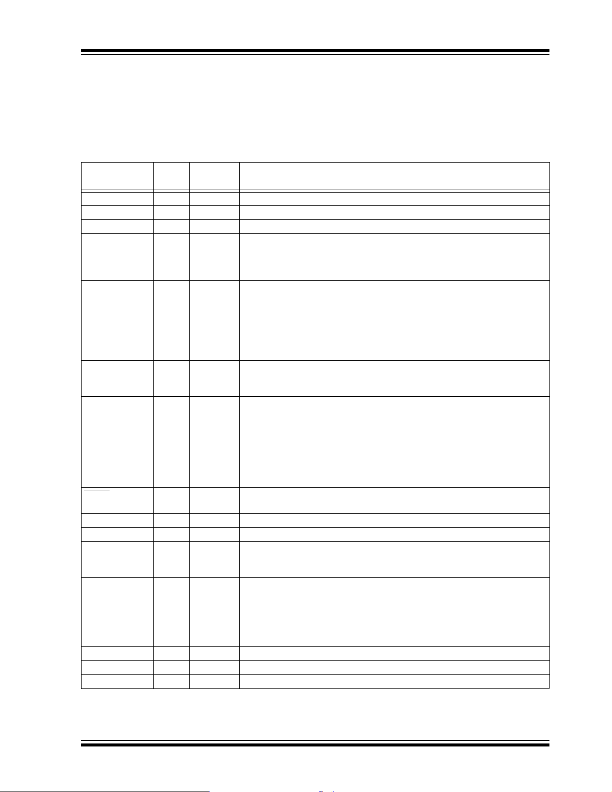
Table 1-1 provides a brief description of device I/O
pinouts for the ds PIC30F1010 and the functions that
may be multiple xed to a port pin. Mul tiple functio ns may
exist on one port pin. When multiplexing occurs, the
peripheral module’s functional requirements may force
an override of the data direction of the port pin.
TABLE 1-1: PINOUT I/O DESCRIPTIONS FOR dsPIC30F1010
Pin Name
AN0-AN5 I Analog Analog input channels.
DD P P Positive supply for analog module.
AV
AVSS P P Ground reference for analog module.
CLKI
CLKO
EMUD
EMUC
EMUD1
EMUC1
EMUD2
EMUC2
Pin
Type
I
O
I/O
I/O
I/O
I/O
I/O
I/O
Buffer
Type
ST/CMOS—External clock source input. Always associated with OSC1 pin function.
Oscillator crystal output. Connects to crystal or resonator in Crystal
Oscillator mode. Opti onally fu nctions a s CLKO in RC and EC mode s. Always
associated with OSC2 pin function.
ST
ST
ST
ST
ST
ST
ICD Primary Communication Channel data input/output pin.
ICD Primary Communication Channel clock input/output pin.
ICD Secondary Communication Channel data input/output pin.
ICD Secondary Communication Channel clock input/output pin.
ICD Tertiary Communication Channel data input/output pin.
ICD Tertiary Communication Channel clock input/output pin.
Description
INT0
INT1
INT2
SFLT1
SFLT2
SFLT3
PWM1L
PWM1H
PWM2L
PWM2H
MCLR
OC1 O — Compare outputs.
OCFLTA I ST Output Compare Fault Pin
OSC1
OSC2
PGD
PGC
PGD1
PGC1
PGD2
PGC2
RB0-RB7 I/O ST PORTB is a bidirectional I/O port.
RA9 I/O ST PORTA is a bidirectional I/O port.
RD0 I/O ST PORTD is a bidirectional I/O port.
Legend: CMOS = CMOS compati ble input or output Analog = Analog input
ST = Schmitt Trigger input with CMOS levels O = Output
I = Input P = Power
I
I
I
I
I
I
O
O
O
O
I/P ST Master Clear (Reset) input or programming voltage input. This pin is an
I
I/O
I/O
I
I/O
I
I/0
I
ST
ST
ST
ST
ST
ST
—
—
—
—
CMOS—Oscillator crystal input.
ST
ST
ST
ST
ST
ST
External interrupt 0
External interrupt 1
External interrupt 2
Shared Fault Pin 1
Shared Fault Pin 2
Shared Fault Pin 3
PWM 1 Low output
PWM 1 High output
PWM 2 Low output
PWM 2 High output
active low Reset to the device.
Oscillator cryst al outpu t. Conne cts t o crys tal or resonator in Crys tal O scillato r
mode. Optionally functions as CLKO in FRC and EC modes.
In-Circuit Serial Programming™ data input/outpu t pin.
In-Circuit Serial Programming clock input pin.
In-Circuit Serial Programming data input/output pin 1.
In-Circuit Serial Programming clock input pin 1.
In-Circuit Serial Programming data input/output pin 2.
In-Circuit Serial Programming clock input pin 2.
© 2006 Microchip Technology Inc. Preliminary DS70178C-page 11

dsPIC30F1010/202X
TABLE 1-1: PINOUT I/O DESCRIPTIONS FOR dsPIC30F1010 (CONTINUED)
Pin Name
RE0-RE7 I/O ST PORTE is a bidirectional I/O port.
RF6, RF7, RF8
SCK1
SDI1
SDO1
SCL
SDA
T1CK
T2CK
U1RX
U1TX
U1ARX
U1ATX
CMP1A
CMP1B
CMP1C
CMP1D
CMP2A
CMP2B
CMP2C
CMP2D
CN0-CN7 I ST Input Change notification inputs
DD P — Positive supply for logic and I/O pins.
V
VSS P — Ground reference for logic and I/O pins.
EXTREF I Analog External reference to Comparator DAC
Legend: CMOS = CMOS compati ble input or output Analog = Analog input
ST = Schmitt Trigger input with CMOS levels O = Output
I = Input P = Power
Pin
Type
I/O ST PORTF is a bidirectional I/O port.
I/O
I
O
I/O
I/O
I
I
I
O
I
O
I
I
I
I
I
I
I
I
Buffer
Type
ST
ST
—
ST
ST
ST
ST
ST
—
ST
—
Analog
Analog
Analog
Analog
Analog
Analog
Analog
Analog
Description
Synchronous serial clock input/output for SPI #1.
SPI #1 Data In.
SPI #1 Data Out.
Synchronous serial clock input/output for I2C™.
Synchronous serial data input/output for I
Timer1 external clock input.
Timer2 external clock input.
UART1 Receive.
UART1 Transmit.
Alternate UART1 Receiv e.
Alternate UART1 Transmit.
Comparator 1 Channel A
Comparator 1 Channel B
Comparator 1 Channel C
Comparator 1 Channel D
Comparator 2 Channel A
Comparator 2 Channel B
Comparator 2 Channel C
Comparator 2 Channel D
Can be software programmed for internal weak pull-ups on all inputs.
2
C.
DS70178C-page 12 Preliminary © 2006 Microchip Technology Inc.
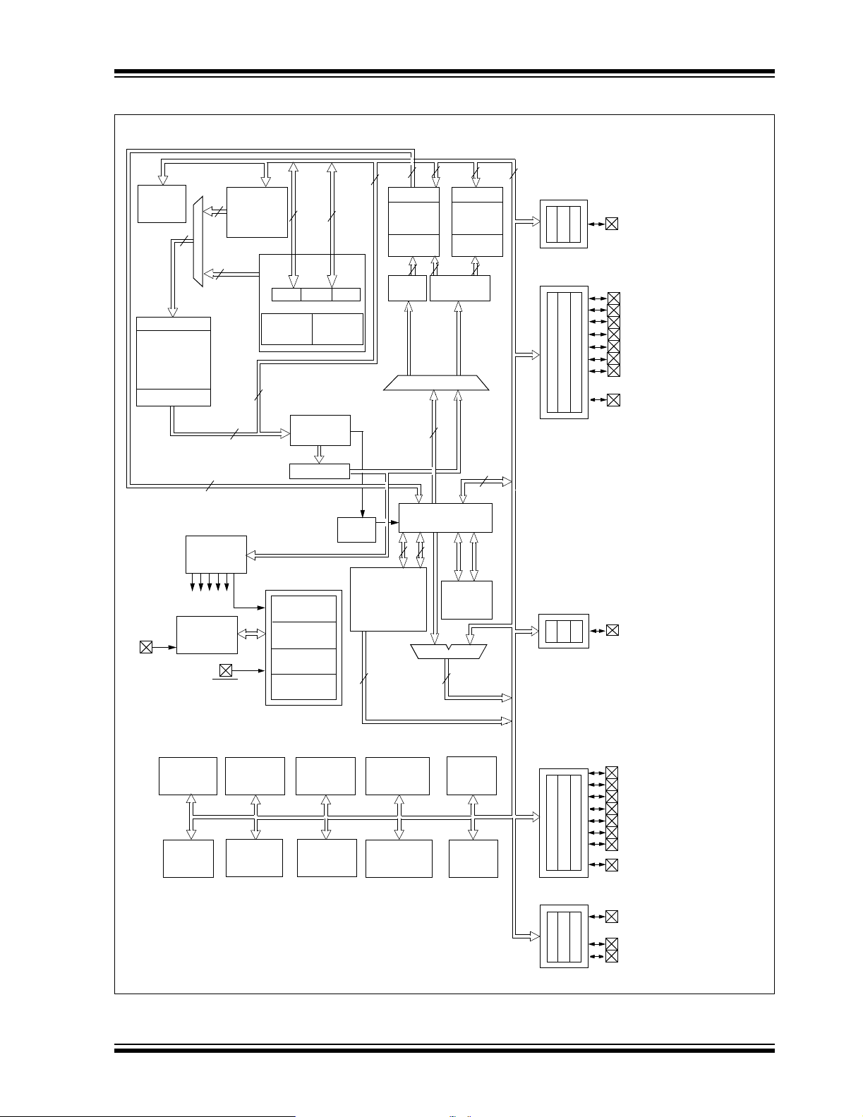
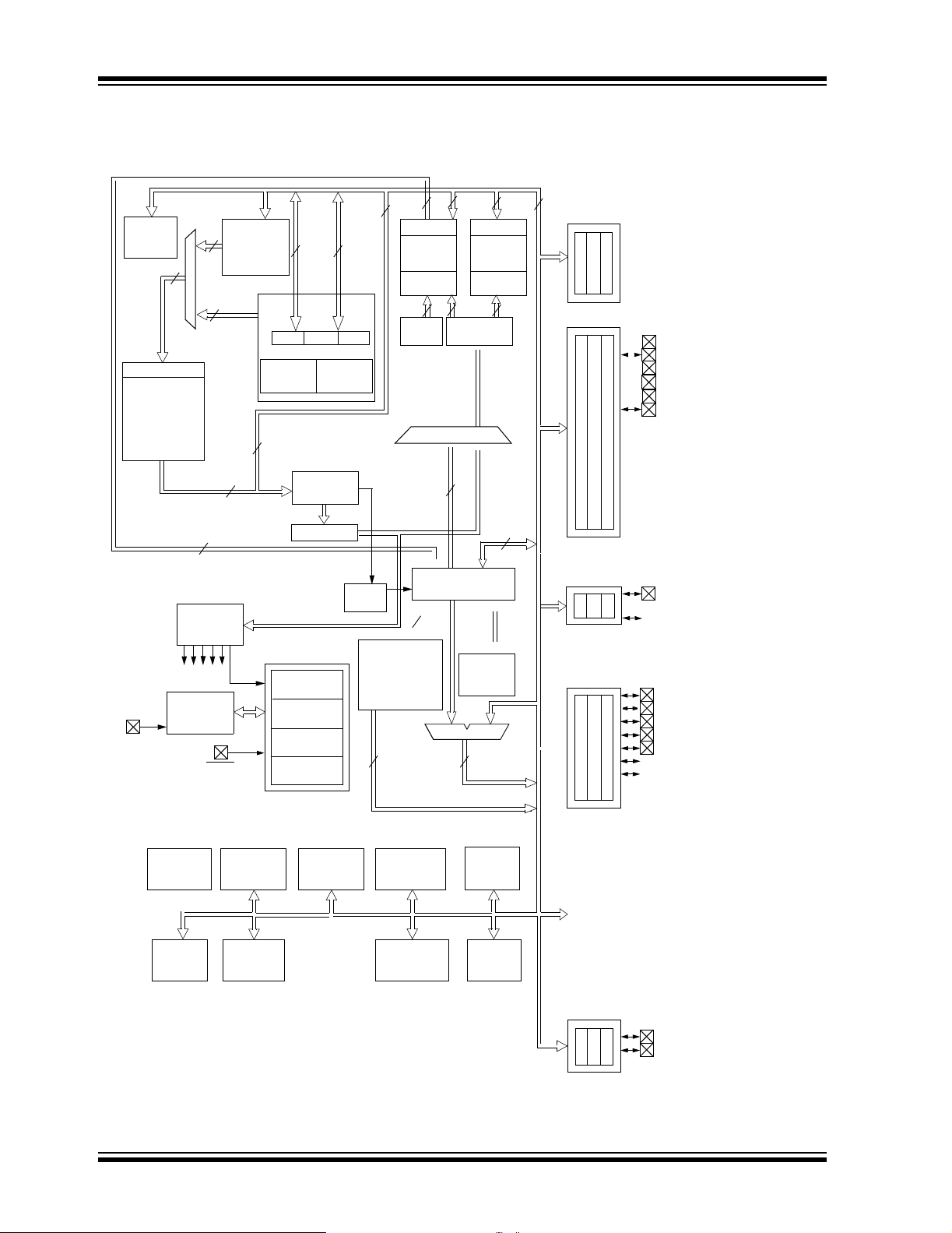
FIGURE 1-2: dsPIC30F2020 BLOCK DIAGRAM
/
dsPIC30F1010/202X
Interrupt
Controller
24
Address Latch
Program Memory
(12 Kbytes)
Data Latch
Instruction
Decode &
24
24
16
Control
PSV & Table
Data Access
Control Block
Stack
Control
16
24
Y Data Bus
8
16
PCH PCL
PCU
Program Counter
Logic
Loop
Control
Logic
ROM Latch
IR
Decode
16
16
Y Data
RAM
(256 bytes)
Address
Latch
Y AGU
Effective Address
16
X Data Bus
16
Data LatchData Latch
X Data
(256 bytes)
Address
16
16
X RAGU
X WAGU
16
16 x 16
W Reg Array
16
16
RAM
Latch
16
SFLT2/INT0/OCFLTA/RA9
16
16
PORTA
PORTB
AN0/CMP1A/CN2/RB0
AN1/CMP1B/CN3/RB1
AN2/CMP1C/CMP2A/CN4/RB2
AN3/CMP1D/CMP2B/CN5/RB3
AN4/CMP2C/CMP3A/CN6/RB4
AN5/CMP2D/CMP3B/CN7/RB5
AN6/CMP3C/CMP4A/
OSC1/CLKI/RB6
AN7/CMP3D/CMP4B/
OSC2/CLKO/RB7
Control Signals
to Various Blocks
OSC1/CLK1
Comparator
Module
Timing
Generation
MCLR
10-bit ADC
Timers
Power-up
Timer
Oscillator
Start-up Timer
POR
Reset
Watchdog
Timer
Input
Capture
Module
Input
Change
Notification
DSP
Engine
16
Compare
Module
SMPS
PWM
Output
Divide
Unit
ALU<16>
16
UART1SPI1
I2C™
PORTD
PORTE
PORTF
PGC2/EMUC2/OC1/SFLT1/IC1/
INT1/RD0
PWM1L/RE0
PWM1H/RE1
PWM2L/RE2
PWM2H/RE3
PWM3L/RE4
PWM3H/RE5
PGC1/EMUC1/EXTREF/PWM4L/
U1ARX/CN0/RE6
T1CK/
PGD1/EMUD1/PWM4H/T2CK/
U1ATX/CN1/RE7
PGD2/EMUD2/SCK1/SFLT3/OC2
INT2/RF6
PGC/EMUC/SDI1/SDA/U1RX/RF7
PGD/EMUD/SD01/SCL/U1TX/RF8
© 2006 Microchip Technology Inc. Preliminary DS70178C-page 13
dsPIC30F1010/202X
Table 1-2 provides a brief description of device I/O
pinouts for the ds PIC30F2020 and the functions that
may be multiple xed to a port pin. Mul tiple functio ns may
exist on one port pin. When multiplexing occurs, the
peripheral module’s functional requirements may force
an override of the data direction of the port pin.
TABLE 1-2: PINOUT I/O DESCRIPTIONS FOR dsPIC30F2020
Pin Name
AN0-AN7 I Analog Analog input channels.
DD P P Positive supply for analog module.
AV
AVSS P P Ground reference for analog module.
CLKI
CLKO
EMUD
EMUC
EMUD1
EMUC1
EMUD2
EMUC2
IC1 I ST Capture input.
INT0
INT1
INT2
SFLT1
SFLT2
SFLT3
PWM1L
PWM1H
PWM2L
PWM2H
PWM3L
PWM3H
PWM4L
PWM4H
MCLR
OC1-OC2
OCFLTA
OSC1
OSC2
PGD
PGC
PGD1
PGC1
PGD2
PGC2
Legend: CMOS = CMOS compatible input or output Analog = Analog input
ST = Schmitt Trigger input with CMOS levels O = Output
I = Input P = Power
Pin
Type
I
O
I/O
I/O
I/O
I/O
I/O
I/O
I
I
I
I
I
I
O
O
O
O
O
O
O
O
I/P ST Master Clear (Reset) input or programming voltage input. This pin is an
O
I
I
I/O
I/O
I
I/O
I
I/O
I
Buffer
Type
ST/CMOS—External clock source input. Always associated with OSC1 pin function.
Oscillator crystal output. Connects to crystal or resonator in Crystal
Oscillator mode. Opti onally fu nctions a s CLKO in RC an d EC modes. Al ways
associated with OSC2 pin function.
ST
ST
ST
ST
ST
ST
ST
ST
ST
ST
ST
ST
—
—
—
—
—
—
—
—
— Compare outputs.
CMOS—Oscillator crystal input.
ST
ST
ST
ST
ST
ST
ICD Primary Communication Channel data input/output pin.
ICD Primary Communication Channel clock input/output pin.
ICD Secondary Communication Channel data input/output pin.
ICD Secondary Communication Channel clock input/output pin.
ICD Tertiary Communication Channel data input/output pin.
ICD Tertiary Communication Channel clock input/output pin.
External interrupt 0
External interrupt 1
External interrupt 2
Shared Fault Pin 1
Shared Fault Pin 2
Shared Fault Pin 3
PWM 1 Low output
PWM 1 High output
PWM 2 Low output
PWM 2 High output
PWM 3 Low output
PWM 3 High output
PWM 4 Low output
PWM 4 High output
active low Reset to the device.
Output Compar e Fault pin
Oscillator cryst al outpu t. Conne cts t o crys tal or resonator in Crys tal O scillato r
mode. Optionally functions as CLKO in FRC and EC modes.
In-Circuit Serial Programming™ data input/outpu t pin.
In-Circuit Serial Programming clock input pin.
In-Circuit Serial Programming data input/output pin 1.
In-Circuit Serial Programming clock input pin 1.
In-Circuit Serial Programming data input/output pin 2.
In-Circuit Serial Programming clock input pin 2.
Description
DS70178C-page 14 Preliminary © 2006 Microchip Technology Inc.

dsPIC30F1010/202X
TABLE 1-2: PINOUT I/O DESCRIPTIONS FOR dsPIC30F2020 (CONTINUED)
Pin Name
RB0-RB7 I/O ST PORTB is a bidirectional I/O port.
RA9 I/O ST PORTA is a bidirectional I/O port.
RD0 I/O ST PORTD is a bidirectional I/O port.
RE0-RE7 I/O ST PORTE is a bidirectional I/O port.
RF6, RF7, RF8
SCK1
SDI1
SDO1
SCL
SDA
T1CK
T2CK
U1RX
U1TX
U1ARX
U1ATX
CMP1A
CMP1B
CMP1C
CMP1D
CMP2A
CMP2B
CMP2C
CMP2D
CMP3A
CMP3B
CMP3C
CMP3D
CMP4A
CMP4B
CN0-CN7 I ST Input Change notification inputs
DD P — Positive supply for logic and I/O pins.
V
VSS P — Ground reference for logic and I/O pins.
EXTREF I Analog External reference to Comparator DAC
Legend: CMOS = CMOS compatible input or output Analog = Analog input
ST = Schmitt Trigger input with CMOS levels O = Output
I = Input P = Power
Pin
Type
I/O ST PORTF is a bidirectional I/O port.
I/O
I
O
I/O
I/O
I
I
I
O
I
O
I
I
I
I
I
I
I
I
I
I
I
I
I
I
Buffer
Type
ST
ST
—
ST
ST
ST
ST
ST
—
ST
O
Analog
Analog
Analog
Analog
Analog
Analog
Analog
Analog
Analog
Analog
Analog
Analog
Analog
Analog
Description
Synchronous serial clock input/output for SPI #1.
SPI #1 Data In.
SPI #1 Data Out.
Synchronous serial clock input/output for I2C™.
Synchronous serial data input/output for I
Timer1 external clock input.
Timer2 external clock input.
UART1 Receive.
UART1 Transmit.
Alternate UART1 Receiv e.
Alternate UART1 Transmit.
Comparator 1 Channel A
Comparator 1 Channel B
Comparator 1 Channel C
Comparator 1 Channel D
Comparator 2 Channel A
Comparator 2 Channel B
Comparator 2 Channel C
Comparator 2 Channel D
Comparator 3 Channel A
Comparator 3 Channel B
Comparator 3 Channel C
Comparator 3 Channel D
Comparator 4 Channel A
Comparator 4 Channel B
Can be software programmed for internal weak pull-ups on all inputs.
2
C.
© 2006 Microchip Technology Inc. Preliminary DS70178C-page 15
dsPIC30F1010/202X
FIGURE 1-3: dsPIC30F2023 BL OC K DIAGR AM
Interrupt
Controller
24
Address Latch
Program Memory
(12 Kbytes)
Data Latch
Instruction
Decode &
24
24
16
Control
Y Data Bus
16
8
PCH PCL
PCU
Program Counter
16
24
ROM Latch
IR
Decode
Y AGU
Effective Address
X Data Bus
16
16 16
16
16
X RAGU
X WAGU
16
16 x 16
W Reg Array
16
16
16
16
PORTA
AN0/CMP1A/CN2/RB0
AN1/CMP1B/CN3/RB1
AN2/CMP1C/CMP2A/CN4/RB2
AN3/CMP1D/CMP2B/CN5/RB3
AN4/CMP2C/CMP3A/CN6/RB4
AN5/CMP2D/CMP3B/CN7/RB5
PORTB
PORTD
OSC1/CLK1
Timing
Generation
Comparator
MCLR
10-bit ADC
Timers
Power-up
Timer
Oscillator
Start-up Timer
POR
Reset
Watchdog
Timer
Input
Capture
Module
DSP
Engine
16
Output
Compare
Module
Power Supply
PWM
Divide
Unit
ALU<16>
16
UART1SPI1
I2C™
PORTE
PORTG
PWM1L/RE0
PWM1H/RE1
PWM2L/RE2
PWM2H/RE3
PWM3L/RE4
PWM3H/RE5
PGC1/EMUC1/PWM4L/T1CK/
SCL/RG2
SDA/RG3
DS70178C-page 16 Preliminary © 2006 Microchip Technology Inc.
dsPIC30F1010/202X
Table 1-3 provides a brief description of device I/O
pinouts for the ds PIC30F2023 and the functions that
may be multiple xed to a port pin. Mul tiple functio ns may
exist on one port pin. When multiplexing occurs, the
peripheral module’s functional requirements may force
an override of the data direction of the port pin.
TABLE 1-3: PINOUT I/O DESCRIPTIONS FOR dsPIC30F2023
Pin Name
AN0-AN11 I Analog Analog input channels.
DD P P Positive supply for analog module.
AV
AVSS P P Ground reference for analog module.
CLKI
CLKO
EMUD
EMUC
EMUD1
EMUC1
EMUD2
EMUC2
IC1 I ST Capture input.
INT0
INT1
INT2
SFLT1
SFLT2
SFLT3
SFLT4
IFLT2
IFLT4
PWM1L
PWM1H
PWM2L
PWM2H
PWM3L
PWM3H
PWM4L
PWM4H
SYNCO
SYNCI
MCLR
OC1-OC2
OCFLTA
OSC1
OSC2
Legend: CMOS = CMOS compatible input or output Analog = Analog input
ST = Schmitt Trigger input with CMOS levels O = Output
I = Input P = Power
Pin
Type
I
O
I/O
I/O
I/O
I/O
I/O
I/O
I
I
I
I
I
I
I
I
I
O
O
O
O
O
O
O
O
O
I
I/P ST Master Clear (Reset) input or programming voltage input. This pin is an
O
I
I
I/O
Buffer
Type
ST/CMOS—External clock source input. Always associated with OSC1 pin function.
Oscillator crystal output. Connects to crystal or resonator in Crystal
Oscillator mode. Opti onally fun ctions a s CLKO in RC and EC mode s. Always
associated with OSC2 pin function.
ST
ST
ST
ST
ST
ST
ST
ST
ST
ST
ST
ST
ST
ST
ST
—
—
—
—
—
—
—
—
—
ST
—
ST
CMOS—Oscillator crystal input.
ICD Primary Communication Channel data input/output pin.
ICD Primary Communication Channel clock input/output pin.
ICD Secondary Communication Channel data input/output pin.
ICD Secondary Communication Channel clock input/output pin.
ICD Tertiary Communication Channel data input/output pin.
ICD Tertiary Communication Channel clock input/output pin.
External interrupt 0
External interrupt 1
External interrupt 2
Shared Fault 1
Shared Fault 2
Shared Fault 3
Shared Fault 4
Independent Fault 2
Independent Fault 4
PWM 1 Low output
PWM 1 High output
PWM 2 Low output
PWM 2 High output
PWM 3 Low output
PWM 3 High output
PWM 4 Low output
PWM 4 High output
PWM SYNC output
PWM SYNC input
active low Reset to the device.
Compare outputs.
Output Compare Fault condi tion.
Oscillator cryst al outpu t. Conne cts t o crys tal or resonator in Crys tal O scillato r
mode. Optionally functions as CLKO in FRC and EC modes.
Description
© 2006 Microchip Technology Inc. Preliminary DS70178C-page 17

dsPIC30F1010/202X
TABLE 1-3: PINOUT I/O DESCRIPTIONS FOR dsPIC30F2023 (CONTINUED)
Pin Name
PGD
PGC
PGD1
PGC1
PGD2
PGC2
RA8-RA11 I/O ST PORTA is a bidirectional I/O port.
RB0-RB11 I/O ST PORTB is a bidirectional I/O port.
RD0,RD1 I/O ST PORTD is a bidirectional I/O port.
RE0-RE7 I/O ST PORTE is a bidirectional I/O port.
RF2, RF3,
RF6-RF8, RF14,
RF15
RG2, RG3 I/O ST PORTG is a bidirectional I/O port.
SCK1
SDI1
SDO1
SS1
SCL
SDA
T1CK
T2CK
U1RX
U1TX
U1ARX
U1ATX
CMP1A
CMP1B
CMP1C
CMP1D
CMP2A
CMP2B
CMP2C
CMP2D
CMP3A
CMP3B
CMP3C
CMP3D
CMP4A
CMP4B
CMP4C
CMP4D
CN0-CN7 I ST Input Change notification inputs
DD P — Positive supply for logic and I/O pins.
V
SS P — Ground reference for logic and I/O pins.
V
EXTREF I Analog External reference to Comparator DAC
Legend: CMOS = CMOS compatible input or output Analog = Analog input
ST = Schmitt Trigger input with CMOS levels O = Output
I = Input P = Power
Pin
Type
I/O
I
I/O
I
I/O
I
I/O ST PORTF is a bidirectional I/O port.
I/O
I
O
I
I/O
I/O
I
I
I
O
I
O
I
I
I
I
I
I
I
I
I
I
I
I
I
I
I
I
Buffer
Type
ST
ST
ST
ST
ST
ST
ST
ST
—
ST
ST
ST
ST
ST
ST
—
ST
—
Analog
Analog
Analog
Analog
Analog
Analog
Analog
Analog
Analog
Analog
Analog
Analog
Analog
Analog
Analog
Analog
Description
In-Circuit Serial Programming™ data input/outpu t pin.
In-Circuit Serial Programming clock input pin.
In-Circuit Serial Programming data input/output pin 1.
In-Circuit Serial Programming clock input pin 1.
In-Circuit Serial Programming data input/output pin 2.
In-Circuit Serial Programming clock input pin 2.
Synchronous serial clock input/output for SPI #1.
SPI #1 Data In.
SPI #1 Data Out.
SPI #1 Slave Synchronization.
2
Synchronous serial clock input/output for I
Synchronous serial data input/output for I
Timer1 external clock input.
Timer2 external clock input.
UART1 Receive.
UART1 Transmit.
Alternate UART1 Receiv e.
Alternate UART1 Transmit
Comparator 1 Channel A
Comparator 1 Channel B
Comparator 1 Channel C
Comparator 1 Channel D
Comparator 2 Channel A
Comparator 2 Channel B
Comparator 2 Channel C
Comparator 2 Channel D
Comparator 3 Channel A
Comparator 3 Channel B
Comparator 3 Channel C
Comparator 3 Channel D
Comparator 4 Channel A
Comparator 4 Channel B
Comparator 4 Channel C
Comparator 4 Channel D
Can be software programmed for internal weak pull-ups on all inputs.
C.
2
C.
DS70178C-page 18 Preliminary © 2006 Microchip Technology Inc.

dsPIC30F1010/202X
2.0 CPU ARCHITECTURE OVERVIEW
Note: This data sheet summarizes features of this g roup
of dsPIC30F devices and is not intended to be a complete
reference source. For more information on the CPU,
peripherals, register descriptions and general device
functionality, refer to the “dsPIC30F Family Reference
Manual” (DS70046). For more information on t he device
instruction set and programming, refer to the “dsPIC 30F/
33F Programmer’s Reference Manual” (DS70157).
2.1 Core Overview
The core has a 24-bit instruction word. The Program
Counter (PC) is 23 bits wide with the Least Significant
bit (LSb) always clear (see Section 3.1 “Program
Address Space ”), and the Most Significant bit (MSb)
is ignored during no rmal program exec ution, exce pt for
certain specialized instructions. Thus, the PC can
address up to 4M instruction words of user program
space. An instruction prefetch mechanism is used to
help maintain throughput. Program loop constructs,
free from loop count management overhead, are supported usin g the DO and REPEAT instructions, both of
which are interruptible at any point.
The working register array consists of 16x16-bit registers, each of which can act as data, address or offset
registers. One working register (W15) operates as a
software Stack Pointer for interrupts and calls.
The data space is 64 Kbytes (32K words) and is split
into two blocks, referred to as X and Y data memory.
Each block has its own independent Address Generation Unit (AGU). Most instructions operate solely
through the X memory AGU, which provides the
appearance of a single unified data space. The
Multiply-Accu mulate (MAC) class of dual s ource DSP
instructions operate through both the X and Y AGUs,
splitting the data address space into two parts (see
Section 3.2 “Data Address Space”). The X and Y
data space boundary is device-specific and cannot be
altered by the user . Each dat a word consis ts of 2 bytes,
and most instruct ions can address data eith er as words
or bytes.
There are two methods of accessing data stored in
program memory:
• The upper 32 Kbytes of data space memory can be
mapped into the lower half (user space) of program
space at any 16K program word boundary, defined
by the 8-bit Program Space Visibility Page
(PSVPAG) register. This lets any instruction access
program space as if it were data space, with a limitation that the access requires an additional cycle.
Moreover, only the lower 16 bits of each instruction
word can be accessed using this method.
• Linear indirect access of 32K word pages within
program space is als o possibl e using any work ing
register, via table read and write instructio ns.
Table read and write instructions can be used to
access all 24 bits of an instruction word.
Overhead-free circular buffers (modulo addressing)
are supported in both X and Y address spaces. This is
primarily intended to remove the loop overhead for
DSP algorithms.
The X AGU also supports Bit-Reversed Addressing
mode on destination effective addresses, to greatly
simplify input or output data reordering for radix-2 FFT
algorithms. Refer to Secti on 4.0 “Address Generator
Units” for details on modulo and Bit-Reversed
Addressing.
The core supports In here nt (n o op era nd), Relative, Literal, Memory Direct, Register Direct, Register Indirect,
Register Offset and Literal Offset Addressing modes.
Instructions are a ssociated w ith pred efined Addr essing
modes, depending upon their functional requirements.
For most i ns tru c ti o ns , the c or e i s c apa bl e of e xe c ut i ng
a data (or program data) memory read, a working register (data) read, a data memory write and a program
(instruction) memory read per instruction cycle. As a
result, 3-operand instructions are supported, allowing
C = A + B operations to be executed in a single cycle.
A DSP engine has been included to significantly
enhance the core arithmetic capability and throughput.
It features a high-speed 17-bit by 17-bit multiplier, a
40-bit ALU, two 40-bit saturating accumulators and a
40-bit bidirectional b arre l s hi fter. Data in the accum ul ator or any wor kin g regi ste r can be sh ifted up to 15 bi ts
right or 16 bits left in a single cycle. The DSP instructions operate seamles sly with all other in struct ion s and
have been desi gned for o ptimal re al-time p erformanc e.
The MAC class of instructions can concurrently fetch
two data operands from memory, while multiplying two
W registers. To enable this concurrent fetching of data
operands, the data space has been split for these
instructions and linear for all others. This has been
achieved in a transparent and flexible manner, by
dedicating certain working registers to each address
space for the MAC class of instructions.
The core does not support a multi-stage instruction
pipeline. However, a single stage instruction prefetch
mechanism is used, which accesses and partially
decodes instructions a cycle ahead of execution, in
order to maximize available execution time. Most
instructions execute in a single cycle, with certain
exceptions.
The core features a vectored exception processing
structure for traps and interrupts, with 62 independent
vectors. The exceptions consist of up to 8 traps (of
which 4 are reserved ) an d 54 int errup ts. Each interrupt
is prioritized based on a us er-assigned priori ty between
1 and 7 (1 being the lowest priority and 7 being the
highest) in conjunction with a predetermined ‘natural
order’. Traps have fi xed prio rities, ranging from 8 to 15.
© 2006 Microchip Technology Inc. Preliminary DS70178C-page 19

dsPIC30F1010/202X
2.2 Programmer’s Model
The programmer’s model is shown in Figure 2-1 and
consists of 16x16-bit working registers (W0 through
W15), 2x40-bit accumulators (ACCA and ACCB),
STATUS register (SR), Data Table Page register
(TBLPAG), Program Space Visibility Page register
(PSVPAG), DO and REPEAT registers (DOSTART,
DOEND, DCOUNT and RCOUNT), and Program
Counter (PC). The working registers can act as data,
address or offset registers. All registers are memory
mapped. W0 acts as the W register for file register
addressing.
Some of these registers have a shadow register associated with each of them, as shown in Figure 2-1. The
shadow register is used as a temp orary holding reg ister
and can transfer it s con ten ts to or from its host register
upon the occurrence of an event. None of the shadow
registers are accessible directly. The following rules
apply for transfer of registers into and out of shadows.
• PUSH.S and POP.S
W0, W1, W2, W3, SR (DC, N, OV, Z and C bits
only) are transferred.
• DO instruction
DOSTART, DOEND, DCOUNT shadows are
pushed on loop start, and popped on loop end.
When a byte operation is performed on a working register , only th e Least Significan t Byte (LSB) of th e targ et
register is affected. However, a benefit of memory
mapped working registers is that both the Least and
Most Significant Bytes (MSBs) can be manipulated
through byte wide data memory space accesses.
2.2.1 SOFTWARE STACK POINTER/ FRAME POINTER
The dsPIC® DSC devices contain a software stack.
W15 is the dedicated software Stack Pointer (SP), and
will be automatically modified by exception processing
and subroutine ca lls and return s. However , W15 can be
referenced by any instruction in the same manner as all
other W registers. This simplifies the reading, writing
and manipulation of the Stack Pointer (e.g., creating
stack frames).
Note: In order to protect against misaligned
stack accesses , W15<0> is always clear.
W15 is initialized to 0x0800 during a Reset. The user
may reprogram the SP during initialization to any
location within data space.
W14 has been dedicated as a Stack Frame Pointer as
defined by the LNK and ULNK instructions. However,
W14 can be referenced by any instruction in the same
manner as all other W registers.
2.2.2 STATUS REGISTER
The dsPIC D SC core has a 16-b it STATUS Registe r
(SR), the LSB of which is referred to as the SR Low
Byte (SRL) and the MSB as the SR High Byte (SRH).
See Figure 2-1 for SR layout.
SRL contains all the MCU ALU operation status flags
(including the Z bit), as wel l as the CPU Inter rupt Pri ority Level S t atus bits, IPL<2:0>, and the REPEAT active
Status bit, RA. During exception processing, SRL is
concatenated with the MSB of the PC to form a
complete word value, which is then stacked.
The upper byte of the STATUS register contains the
DSP Adder/Subtracter status bits, the DO Loop Active
bit (DA) and the Digit Carry (DC) Status bit.
2.2.3 PROGRAM COUNTER
The Program Counter is 23 bi ts wide. Bit 0 is a lways
clear. Therefore, the PC can address up to 4M
instruction words.
DS70178C-page 20 Preliminary © 2006 Microchip Technology Inc.
FIGURE 2-1: PROGRAMMER’S MODEL
DSP Operand
Registers
DSP Address
Registers
dsPIC30F1010/202X
W0/WREG
W1
W2
W3
W4
W5
W6
W7
W8
W9
W10
W11
W12/DSP Offset
W13/DSP Write Back
W14/Frame Pointer
W15/Stack Pointer
D0D15
PUSH.S Shadow
DO Shadow
Legend
Working Registers
DSP
Accumulators
PC22
7
22
22
TABPAG
TBLPAG
7
PSVPAG
PSVPAG
AD39 AD0AD31
ACCA
ACCB
0
Data Table Page Address
0
SPLIM Stack Pointer Limit Register
Program Space Visibility Page Address
15
RCOUNT
15
DCOUNT
DOSTART
DOEND
PC0
AD15
Program Counter
0
0
REPEAT Loop Counter
0
DO Loop Counter
0
DO Loop Start Address
DO Loop End Address
15
CORCON
OA OB SA SB
© 2006 Microchip Technology Inc. Preliminary DS70178C-page 21
OAB SAB
SRH
DA DC
IPL2 IPL1
RA
IPL0 OV
SRL
N
0
Core Configuration Register
C
Z
STATUS Register

dsPIC30F1010/202X
2.3 Divide Support
The dsPIC DSC devices feature a 16/16-bit signed
fractional divide ope rati on , as w ell as 32/16-bit and 16/
16-bit signed an d unsigned intege r divide operati ons, in
the form of single instruction iterative divides. The
following instructions and data sizes are supported:
1. DIVF – 16/16 signed fractional divide
2. DIV.sd – 32/16 signed divide
3. DIV.ud – 32/16 unsigned divide
4. DIV.sw – 16/16 signed divide
5. DIV.uw – 16/16 unsigned divide
The 16/16 divides are similar to the 32/16 (same number
of iterations), but the dividend is either zero-extended or
sign-extended during the first iteration.
The divide instructions must be executed within a
REPEAT loop. Any other form of exec ution (e.g. a serie s
of discrete divide instruc tions) w ill not function c orrectly
because the instruction flow depends on RCOUNT.
The divide instru ction does not automat icall y set up the
RCOUNT value, and it must, therefore, be explicitly
and correctly specified in the REPEAT instruction, as
shown in Table 2-1 (REPEAT will execute the target
instruction {operand value + 1} times). The REPEAT
loop count must be set up for 18 iterati ons of the DIV/
DIVF instruction. Thus, a complete divide operation
requires 19 cycles.
Note: The Divide flow is interruptible. However,
the user needs to save the context as
appropriate.
TABLE 2-1: DIVIDE INSTRUCTIONS
Instruction Function
DIVF Signed fractional divide: Wm/Wn → W0; Rem → W1
DIV.sd Signed divide: (Wm + 1:Wm)/Wn → W0; Rem → W1
DIV.ud Unsigned divide: (Wm + 1:Wm)/Wn → W0; Rem → W1
DIV.sw Signed divide: Wm / Wn → W0; Rem → W1
DIV.uw Unsigned divide: Wm / Wn → W0; Rem → W1
DS70178C-page 22 Preliminary © 2006 Microchip Technology Inc.
dsPIC30F1010/202X
2.4 DSP Engine
The DSP engine consists of a high speed 17-bit x
17-bit multiplier , a barrel s hifter , and a 40-bit adde r/subtracter (with two target accumulators, round and
saturation logic).
The DSP engine also has the capability to perform inherent accumulator-to-accumulator operations, which
require no additional data. These instructions are ADD,
SUB and NEG.
The DSP engine has various options selected through
various bits in the CPU Core Configuration Register
(CORCON), as listed below:
1. Fractional or integer DSP multiply (IF).
2. Signed or unsigned DSP multiply (US).
3. Conventional or convergent rounding (RND).
4. Automatic saturation on/off for ACCA (SATA).
5. Automatic saturation on/off for ACCB (SATB).
6. Automatic saturation on/off for writes to data
memory (SATDW).
7. Accumulator Saturation mode selection
(ACCSAT).
Note: For CORCON layout, see Table 3-3.
A block diagram of the DSP engine is shown in
Figure 2-2.
TABLE 2-2: DSP INSTRUCTION SUMMARY
Instruction Algebraic Operation ACC WB?
CLR A = 0 Yes
ED A = (x – y)
EDAC A = A + (x – y)
MAC A = A + (x * y) Yes
MAC A = A + x
MOVSAC No change in A Yes
MPY A = x * y No
MPY.N A = – x * y No
MSC A = A – x * y Yes
2
2
2
No
No
No
© 2006 Microchip Technology Inc. Preliminary DS70178C-page 23

dsPIC30F1010/202X
FIGURE 2-2: DSP ENGINE BLOCK DI AGR AM
40
Carry/Borrow Out
Carry/Borrow In
40-bit Accumulator A
40-bit Accumulator B
Saturate
Adder
Negate
40
Round
Logic
S
a
16
t
u
r
a
t
e
40
40
Barrel
Shifter
32
32
40
16
X Data Bus
16
Zero Backfill
40
Sign-Extend
Y Data Bus
33
17-bit
Multiplier/Scaler
16
To/From W Array
DS70178C-page 24 Preliminary © 2006 Microchip Technology Inc.
16

dsPIC30F1010/202X
2.4.1 MULTIPLIER
The 17x17-bit multiplier is capable of signed or
unsigned operati on and can mul tiplex i ts ou tput usi ng a
scaler to support either 1.31 fractional (Q31) or 32-bit
integer results. Unsigned operands are zero-extended
into the 17th bit of the multiplier input value. Signed
operands are sign-exten ded into the 17th bit of the mu ltiplier input value. The output of t he 17x17-bit multip lier/
scaler is a 33-bit value, which is sign-extended to 40
bits. Intege r data is inherently rep resented as a signed
two’s complement value, where the MSB is defined as
a sign bit. Generally speaking, the range of an N-bit
two’s complement integer is -2
bit integer, the data range is -32768 (0x8000) to 32767
(0x7FFF), including 0. For a 32-bit integer, the data
range is -2,147,483,648 (0x8000 0000) to
2,147,483,645 (0x7FFF FFFF).
When the multiplier is configured for fractional multiplication, the data is represented as a two’s complement
fraction, where the M SB is defined as a sign b it and the
radix point is impl ied to lie just after the sign b it (QX format). The range of an N-bit two’s complement fraction
with this implied radix point is -1.0 to (1-2
16-bit fraction, the Q15 data range is -1.0 (0x8000) to
0.999969482 (0x7FFF), including 0, and has a precision of 3.01518x1 0
tiply operation generates a 1.31 product, which has a
precision of 4.65661x10
The same multiplier is used to support the MCU multiply instructions, which include integer 16-bit signed,
unsigned and mixed sign multiplies.
The MUL instruction may be directed to use byte or
word sized operands. By te opera nds wil l direct a 16-bit
result, and word operands will direct a 32-bit result to
the specified register(s) in the W array.
-5
. In Fractional mode, a 16x16 mu l-
-10
N-1
N-1
to 2
– 1. For a 16-
1-N
). For a
.
2.4.2 DATA ACCUMULATORS AND ADDER/SUBTRACTER
The data accumulator consists of a 40-bit adder/
subtracter with automatic sign extension logic. It can
select one of two accumulators (A or B) as its preaccumulation source and post-accumulation destination. For the ADD and LAC instructions, the data to be
accumulated or load ed ca n be optio nally sca led v ia th e
barrel shifter, prior to accumulation.
2.4.2.1 Adder/Subtracter, Overflow and Saturation
The adder/subtracter is a 40-bit adder with an optional
zero input into one side and either true or complement
data into the other input. In the case of addition, the
carry/borrow
true data (not complemented), whereas in the case of
subtraction, the carry/bo rrow
other input is complemented. The adder/subtracter
generates overflow Status bits SA/SB and OA/OB,
which are latched an d reflected i n the ST ATUS register .
• Overflow from bit 39: this is a catastrophic
overflow in which the sign of the accumulator is
destroyed.
• Overflow into guard bits 32 through 39: this is a
recoverable overflow. This bit is set whenever all
the guard bits are not identical to each other.
The adder has an additional saturation block which
controls accumulator data saturation, if selected. It
uses the result of the adder, the overflow Status bits
described above, and the SATA/B (CORCON<7:6>)
and ACCSAT (CORCON<4>) mode control bits to
determine when and to what value to saturate.
Six STATUS register bits have been provided to
support saturation and overflow; they are:
1. OA:
ACCA overflowed into guard bits
2. OB:
ACCB overflowed into guard bits
3. SA:
ACCA saturated (bit 31 overflow and sa turation)
or
ACCA overflowed into guard bits and saturated
(bit 39 overflow and s aturation)
4. SB:
ACCB saturated (bit 31 overflow and sa turation)
or
ACCB overflowed into guard bits and saturated
(bit 39 overflow and s aturation)
5. OAB:
Logical OR of OA and OB
6. SAB:
Logical OR of SA and SB
The OA and OB bits are modified each time data
passes through the adder/subtracter. When set, they
indicate that the most recent operation has overflowed
into the accumulator guard bits (bits 32 through 39).
The OA and OB bits can also optionally generate an
arithmetic warning trap when set and the corresponding overflow trap flag enable bit (OVATE, OVBTE) in
the INTCON1 register (refer to Section 5.0 “Inter-
rupts”) is set. This allows the user to take immediate
action, for example, to correct system gain.
input is active high and the other input is
input is active low and the
© 2006 Microchip Technology Inc. Preliminary DS70178C-page 25

dsPIC30F1010/202X
The SA and SB bits are modified each ti me data pass es
through the adder/subtracter, but can only be cleared by
the user. When set, they indicate that the accumulator
has overflowed its maximum range (bit 31 for 32-bit saturation, or bit 39 for 40-bit saturation) and will be saturated (if saturation is enabled). When saturation is not
enabled, SA and SB default to bit 39 overflow and thus
indicate that a catastrophic overflow has occurred. If the
COVTE bit in the INTCON1 register is set, SA and SB
bits will generate an arithmetic warning trap when
saturation is disabled.
The overflow and saturation Status bits can optionally
be viewed in the STATUS Register (SR) as the logical
OR of OA and OB (in bit OAB) and the logical OR of SA
and SB (in bit SAB). This allows programmers to check
one bit in the STATUS Register to determine if either
accumulator has overflowed, or one bit to determine if
either accumulator has saturated. This is useful for
complex number arithmetic, which typically uses both
the accumulators.
The device supports three Saturation and Overflow
modes.
1. Bit 39 Overflow and Saturation:
When bit 39 overflow and saturation occurs, the
saturation logic loads the maximally positive 9.31
(0x7FFFFFFFFF) or maximally negative 9.31
value (0x8000000000) into the target accumulator. The SA or SB bit is set and remains set until
cleared by the user. This is referred to as ‘super
saturation’ and provides protection against erroneous data or unexpected algorithm problems
(e.g., gain calculations).
2. Bit 31 Overflow and Saturation:
When bit 31 overflow and saturation occurs, the
saturation logic then loads the maximally positive
1.31 value (0x007FFFFFFF) or maximally negative 1.31 value (0x0080000000) into the target
accumulator . The SA or SB bit is set and rem ains
set until cleared by the user . When this Saturation
mode is in effect, the guard bits are not used (so
the OA, OB or OAB bits are never set).
3. Bit 39 Catastrophic Overflow
The bit 39 overflow Status bit from the adder is
used to set the SA or SB bit, which remain set
until cleared by the user. No saturation operation
is performed and the accumulator is allowed to
overflow (destroying it s sign). If the C OVTE bit in
the INTCON1 register is set, a catastrophic
overflow can initiate a trap exception.
2.4.2.2 Accumulator ‘Write Back’
The MAC class of instructions (with the exception of
MPY, MPY.N, ED and EDAC) can optionally write a
rounded version of the high word (bits 31 through 16)
of the accumulator that is not targeted by the instructio n
into data spac e memory. The write is performed across
the X bus into combined X and Y address space. The
following addressing modes are supported:
1. W13, Register Direct:
The rounded contents of the non-target
accumulator are written into W13 as a 1.15
fraction.
2. [W13] + = 2, Register Indirect with Post-Increment: The rounded contents of the non-target
accumulator are wri tten into the ad dress pointed
to by W13 as a 1.15 fraction. W13 is then
incremented by 2 (for a word write).
2.4.2.3 Round Logic
The round logic is a combinational block, which performs a conventional (biased) or convergent (unbiased)
round function during an accumulator write (store). The
Round mode is determined by the state of the RND bit
in the CORCON register. It generates a 16-bit, 1.15 data
value which is passed to the data space write saturation
logic. If rounding is not indicated by the instruction, a
truncated 1.15 data value is stored and the least
significant word (lsw) is simply discarded.
Conventional rounding takes bit 15 of the accumulator,
zero-extends it and ad ds it to the AC CxH w ord (bi t s 16
through 31 of the accumulato r). If the ACCxL word (bit s
0 through 15 of the accumulator) is between 0x8000
and 0xFFFF (0x8000 included), ACCxH is incremented. If ACCxL is between 0x0000 and 0x7FFF,
ACCxH is left unchanged. A consequence of this
algorithm is that over a succ ession of ran dom roundin g
operations, the value will tend to be biased slightly
positive.
Convergent (or unbiased) rounding operates in the
same manner as conventional rounding, except when
ACCxL equals 0x8000. If this is the case, the LSb (bit
16 of the accumu lator) of ACCxH is examined. If it is ‘1’,
ACCxH is inc rement ed. If it is ‘0’, ACCxH is not modified. Assuming that bit 16 is effectively random in
nature, this scheme w i ll re mo ve any rou ndi ng b ias th at
may accumulate.
The SAC and SAC.R instructions store either a truncated (SAC) or rounded (SAC.R) version of the c ontents
of the target accumul ator to data mem ory , via the X bu s
(subject to data saturation, see Section 2.4.2.4 “Data
Space Write Saturation”). Note that for the MAC cl as s
of instructions, the accumulator write back operation
will function in the s ame mann er , a ddressing co mbine d
MCU (X and Y) data space though the X bus. For this
class of instructions, the data is always subject to
rounding.
DS70178C-page 26 Preliminary © 2006 Microchip Technology Inc.

dsPIC30F1010/202X
2.4.2.4 Data Space Write Saturation
In addition to adder/subtrac ter saturation, writes to dat a
space may also be saturated, but without affecting the
contents of the source accumulator. The data space
write saturation logic block accepts a 16-bit, 1.15 fractional value from the round logic block as its input,
together with overflow status from the original source
(accumulator) and the 16-bit round adder. These are
combined and used t o sele ct the a ppr opriate 1.15 fra ctional value as output to write to data space memory.
If the SATDW bit in the CORCON register is set, data
(after rounding or truncation) is tes te d for ove rflo w and
adjusted accordingly. For input data greater than
0x007FFF, data written to memo ry is forced to the maximum positi ve 1. 15 val ue, 0x 7FFF. For input data less
than 0xFF8000, da ta wr itten to me mory i s forced to th e
maximum negative 1.1 5 value, 0x8000. The MSb of the
source (bit 39) is used to determine the sign of the
operand being tested.
If the SA TDW bi t in the CORCON regis ter is not set , the
input data is always passed through unmodified under
all conditions.
2.4.3 BARREL SHIFTER
The barrel shifter is capable of performing up to 15-bit
arithmetic or logic right shifts, or up to 16-bit left shifts
in a single c ycle. The sou rce can be ei ther of th e two
DSP accumulators or the X bus (to support multi-bit
shifts of register or memory data).
The shifter requi res a signed binary value to determine
both the magnitude (num ber of bits) and direction of the
shift operation. A positive value will shift the operand
right. A negative value will shift the operand left. A
value of ‘0’ will not modify the operand.
The barrel shifter is 40 bits wide, thereby obtaining a
40-bit result for DSP shift operati ons and a 16- bit result
for MCU shift operations. Data from the X bus is presented to the barrel shifter between bit positions 16 to
31 for right shifts, and bit positio ns 0 to 15 for left shift s.
© 2006 Microchip Technology Inc. Preliminary DS70178C-page 27

dsPIC30F1010/202X
NOTES:
DS70178C-page 28 Preliminary © 2006 Microchip Technology Inc.

dsPIC30F1010/202X
3.0 MEMORY ORGANIZATION
Note: This data sheet summarizes features of this g roup
of dsPIC30F devices and is not intended to be a complete
reference source. For more information on the CPU,
peripherals, register descriptions and general device
functionality, refer to the “dsPIC30F Family Reference
Manual” (DS70046). For more information on t he device
instruction set and programming, refer to the “dsPIC 30F/
33F Programmer’s Reference Manual” (DS70157).
3.1 Program Address Space
The program address space is 4M instruction words. It
is addressable by a 24-bit value from either the 23-bit
PC, table instruction Effective Address (EA), or data
space EA, when program space is mapped into data
space, as defined by Table 3-1. Note that the program
space address i s incr ement ed by two betw een suc cessive program words, in order to provide compatibility
with data space addressing.
User program space access is restricted to the lower
4M instruction word address range (0x000000 to
0x7FFFFE), for all acce sses other than TBLRD/TBLWT,
which use TBLPAG<7> to determine user or configuration space access. In Table 3-1, Read/Write instructions, bit 23 allows access to the Device ID, the User ID
and the Configuration bits. Otherwise, bit 23 is always
clear.
FIGURE 3-1:
Space
User Memory
PROGRAM SPACE MEMORY
MAP FOR dsPIC3 0F1010/
202X
Reset – GOTO Instruction
Reset – Target Address
Reserved
Ext. Osc. Fail Trap
Address Error Trap
Stack Error Trap
Arithmetic Warn. Trap
Reserved
Reserved
Reserved
Vector 0
Vector 1
Vector 52
Vector 53
Alternate Vector Table
User Flash
Program Memory
(4K instructions)
Reserved
(Read 0’s)
000000
000002
000004
000014
00007E
000080
0000FE
000100
001FFE
002000
7FFFFE
800000
Vector Tables
Note: The address map shown in Figure 3-1 is
conceptual, and the actual memory configuration may vary across individual
devices depending on available memory.
Reserved
8005BE
Space
Configuration Memory
UNITID (32 instr.)
Reserved
Device Configuration
Registers
Reserved
8005C0
8005FE
800600
F7FFFE
F80000
F8000E
F80010
FEFFFE
DEVID (2)
© 2006 Microchip Technology Inc. Preliminary DS70178C-page 29
FF0000
FFFFFE

dsPIC30F1010/202X
TABLE 3-1: PROGRAM SPACE ADDRESS CONSTRUCTION
Access Type
Access
Space
<23> <22:16> <15> <14:1> <0>
Instruction Access User 0 PC<22:1> 0
TBLRD/TBLWT User
TBLPAG<7:0> Data EA <15:0>
(TBLPAG<7> = 0)
TBLRD/TBLWT Configuration
TBLPAG<7:0> Data EA <15:0>
(TBLPAG<7> = 1)
Program Space Visibility User 0 PSVPAG<7:0> Data EA <14:0>
FIGURE 3-2: DATA ACCESS FROM PROGRAM SPA CE A DDRESS GEN ERATION
23 bits
Using
Program
Counter
0
Program Space Address
0Program Counter
Select
Using
Program
Space
Visibility
Using
Table
Instruction
Note: Program Space Visibility cannot be used to access bits <23:16> of a word in program memory.
0
1/0
User/
Configuration
Space
Select
PSVPAG Reg
8 bits
TBLPA G Reg
8 bits
1
24-bit EA
EA
15 bits
EA
16 bits
Byte
Select
DS70178C-page 30 Preliminary © 2006 Microchip Technology Inc.

dsPIC30F1010/202X
3.1.1 DATA ACCESS FROM PROGRAM MEMORY USING TABLE INSTRUCTIONS
This architecture fetc hes 24 -bi t w ide prog ram me mo ry.
Consequently, instructions are always aligned. However, as the architecture is modified Harvard, data can
also be present in program space.
There are two methods by which program space can
be accessed; via special table instructions, or through
the remapping of a 16 K word program space page into
the upper half o f da ta space (see Section 3.1.2 “Data
Access from Program Memory Using Program
Space Visibility”). The TBLRDL and TBLWTL instruc-
tions offer a direct m ethod of reading or w riting the least
significant word (lsw) of any address within program
space, without going through data space. The TBLRDH
and TBLWTH instructions are the only method whereby
the upper 8 bits of a program space word can be
accessed as data.
The PC is incremented by two for each successive
24-bit program word. This allows program memory
addresses to directly map to data space addresses.
Program memory can thus be regarded as two 16-bit
word wide address sp ac es , res id ing sid e by si de, each
with the same address range. TBLRDL and TBLWTL
access the space which contains the Least Significant
Data Word, and TBLRDH and TBLWTH access the
space which contains the Most Significant Data Byte.
Figure 3-2 shows how the EA is created for table operations and data space accesses (PSV = 1). Here,
P<23:0> refers to a program space word, whereas
D<15:0> refers to a data space word.
A set of Table Instructions is prov ided to move by te o r
word sized data to and from program space.
1. TBLRDL: Table Read Low
Word: Read the lsw of the program address;
P<15:0> maps to D<15:0>.
Byte: Read one of the LSBs of the program
address;
P<7:0> maps to the destination byte when byte
select = 0;
P<15:8> maps to the d estination b yte when byte
select = 1.
2. TBLWTL: Tabl e Writ e Low (re fer to Section 7.0
“Flash Program Memory” for details on Flash
Programming).
3. TBLRDH: Table Read High
Word: Read the most significant word of the
program address;
P<23:16> maps to D<7:0>; D<15:8> always
be = 0.
Byte: Read one of the MSBs of the program
address;
P<23:16> maps to the destination byte when
byte select = 0;
The destination byte will al ways be = 0 when
byte select = 1.
4. TBLWTH: Table Write High (refer to Section 7.0
“Flash Program Memory” for details on Flash
Programming).
FIGURE 3-3: PROGRAM DATA T ABLE A CCESS (LEAST SI GNIFICANT WO RD)
PC Address
0x000000
0x000002
0x000004
0x000006
Program Memory
‘Phantom’ Byte
(Read as ‘0’).
00000000
00000000
00000000
00000000
23
TBLRDL.W
16
8
TBLRDL.B (Wn<0> = 0)
TBLRDL.B (Wn<0> = 1)
0
© 2006 Microchip Technology Inc. Preliminary DS70178C-page 31

dsPIC30F1010/202X
FIGURE 3-4: PROGRAM DATA T ABLE ACCESS (M OST SI GNIFICANT BYTE)
TBLRDH.W
PC Address
0x000000
0x000002
0x000004
0x000006
Program Memory
‘Phantom’ Byte
(Read as ‘0’)
00000000
00000000
00000000
00000000
23
TBLRDH.B (Wn<0> = 1)
3.1.2 DATA ACCESS FROM PROGRAM MEMORY USING PROGRAM SPACE VISIBILITY
The upper 32 Kbytes of data space may optionally be
mapped into any 16K word program space page. This
provides transparent access of stored constant data
from X data space, without the need to use special
instructions (i.e., TBLRDL/H, TBLWTL/H instructions).
Program space access through the data space occurs
if the MSb of the data space EA is set and program
space visibility is enabled, by setting the PSV bit in the
Core Control register (CORCON). The functions of
CORCON are discussed in Section 2.4 “DSP
Engine”.
Data accesses to this area add an additional cycle to
the instruction being executed, since two program
memory fetches are required.
Note that the upper half of addressable data space is
always part of the X data space. Therefore, when a
DSP operation uses program sp ace mapp ing to acc ess
this memory region , Y d at a space should typically contain state (variable) data for DSP operations, whereas
X data space should typically contain coefficient
(constant) data.
Although each da ta sp ace addres s, 0x8000 and higher ,
maps directly into a corresponding program memory
address (see Figure 3-5), only the lower 16-bits of the
24-bit program word are used to contain the data. The
upper 8 bits shoul d be progra mmed to forc e an illeg al
instruction to maintain machine robustness. Refer to
the “dsPIC30F/33F Programmer’s Reference Manual”
(DS70157) for details on instruction encoding.
16
TBLRDH.B (Wn<0> = 0)
Note that by incrementing the PC by 2 for each program memory word, the Least Significant 15 bits of
data space addresses directly map to the Least Significant 15 bits in the corresponding program space
addresses. The rem aining b its a re provid ed by th e Program Space Vis ibilit y Page regi ster, PSVPAG<7:0>, as
shown in Figure 3-5.
Note: PSV access is tempor arily dis abled d uring
Table Reads/Writes.
For instructions that use PSV which are executed
outside a REPEAT loop:
• The following instructions will require one instruction cycle in addition to the specified execution
time:
- MAC class of instructions with data operand
prefetch
- MOV instructions
- MOV.D instructions
• All other instructions will require two instruction
cycles in addition to the specified execution time
of the instruction.
For instructions that use PSV which are executed
inside a REPEAT loop:
• The following inst ances wi ll require two ins truction
cycles in addition to the specified execution time
of the instruction:
- Execution in the first iteration
- Execution in the last iteration
- Execution prior to exiting the loop due to an
interrupt
- Execution upon re-entering the loop after an
interrupt is serviced
• Any other iteration of the REPEAT loop will allow
the instruction, accessing data using PSV, to
execute in a single cycle.
8
0
DS70178C-page 32 Preliminary © 2006 Microchip Technology Inc.

dsPIC30F1010/202X
FIGURE 3-5 : DATA S PACE WINDOW INTO PRO GR AM S PACE OPERATION
Data
Space
EA
EA<15> =
16
EA<15> = 1
15
0
15
PSVPAG
(1)
23 15 0
3.2 Data Address Sp ace
The core has two data spaces. The data spaces can be
considered either separate (for some DSP instructions), or as one unified linear address range (for MCU
instructions). The dat a spaces are accessed using two
Address Generation Units (AGUs) and separate data
paths.
3.2.1 DATA SPACE MEMORY MAP
The data space memory is split into two blocks, X and
Y data space. A key element of this architectur e is th at
Y space is a subset of X space, and is fully contained
within X space. In order to provide an apparent linear
addressing space, X and Y spaces have contiguous
addresses.
© 2006 Microchip Technology Inc. Preliminary DS70178C-page 33
When executing any instruction other than one of the
MAC class of instructions, the X block consists of the
256 byte data address space (including all Y
addresses). When executing one of the MAC class of
instructions, the X block consists of the 256 bytes data
address space excluding the Y address block (for data
reads only). In other word s, all other i nstructions rega rd
the entire data memory as one composite address
space. The MAC class instructions extract the Y
address space from data space and address it using
EAs sourced from W10 and W11. The remaining X data
space is addressed using W8 and W9. Both address
spaces are concurrently accessed only with the MAC
class instructions.
A data space memory map is shown in Figure 3-6.

dsPIC30F1010/202X
FIGURE 3-6: DA TA SP ACE MEMO R Y MA P
SFR Space
(Note)
512 bytes
SRAM Space
MSB
Address
0x0001
0x07FF
0x0801
0x08FF
0x0901
0x09FF
0x8001
16 bits
SFR Space
X Data RAM (X)
256 bytes
Y Data RAM (Y)
256 bytes
(See Note)
LSB
Address
LSBMSB
0x0000
0x07FE
0x0800
2560 bytes
Near
Data
Space
0x08FE
0x0900
0x09FE
0x0A00
0x8000
X Data
Unimplemented (X)
Optionally
Mapped
into Program
Memory
0xFFFF
Note: Unimplemented SFR or SRAM locations read as ‘0’.
0xFFFE
DS70178C-page 34 Preliminary © 2006 Microchip Technology Inc.

dsPIC30F1010/202X
FIGURE 3-7: DATA SPACE FOR MCU AND DSP (MAC CLASS) INSTRUCTIONS
SFR SPACE
UNUSED
(Y SPACE)
X SPACE
Non-MAC Class Ops (Read/Write) MAC Class Ops Read-Only
MAC Class Ops (Wr i te)
Indirect EA using any W Indirect EA using W10, W11
Y SPACE
UNUSED
SFR SPACE
UNUSED
Indirect EA using W8, W9
X SPACE
X SPACE
© 2006 Microchip Technology Inc. Preliminary DS70178C-page 35

dsPIC30F1010/202X
3.2.2 DATA SPACES
The X data space is used by all instructions and supports all Addressing modes. There are separate read
and write data buses. The X read data bus is the return
data path for all inst ructions that view data spac e as
combined X and Y address space. It is also the X
address space data path for the dual operand read
instructions (MAC class). The X write data bus is the
only write path to data space for all instructions.
The X data space also suppo rt s modulo addre ssing for
all instructions, subject to Addressing mode restrictions. Bit-Reversed Addressing is only supported for
writes to X data space.
The Y data space is used in concert with the X data
space by the MAC class of instructions (CLR, ED,
EDAC, MAC, MOVSAC, MPY, MPY.N and MSC) to provide two concurrent data read paths. No writes occur
across the Y bus. This class of instructions dedicates
two W register pointers, W10 and W11, to always
address Y data space, independent of X data space,
whereas W8 and W9 always address X data space.
Note that during accumulator write back, the data
address space is con si dere d a c om bin ati on of X and Y
data spaces, so the write occurs across the X bus.
Consequently, the write can be to any address in the
entire data space.
The Y data space can only be used for the data
prefetch operation associated with the MAC class of
instructions. It also supports modulo addressing for
automated circular bu f fe rs. O f c ours e, all othe r ins tru ctions can access the Y dat a address sp ace through the
X data path, as part of the composite linear space.
The boundary between the X and Y data spaces is
defined as shown in Figure 3-6 and is not user programmable. Shoul d an EA poin t to d ata out side it s own
assigned address space, or to a location outside physical memory, an all-zero word/byte will be returne d. For
example, although Y address space is visible by all
non-MAC instructions using any Addressing mode, an
attempt by a MAC instruction to fetch data from that
space, usin g W8 or W9 (X spac e point ers), wi ll ret urn
0x0000.
3.2.3 DATA SPACE WIDTH
The core data width is 16 bits. All internal registers are
organized as 16-bit wide words. Data space memory is
organized in byte addressable, 16-bit wide blocks.
3.2.4 DATA ALIGNMENT
To help maintain backward compatibility with PIC
MCU devices and improve data space memory usage
efficiency, the dsPIC30F instruction set supports both
word and byte operation s. Data i s aligned in dat a memory and registers as words, but all data space EAs
resolve to bytes. Data byte reads will rea d the comp lete
word, which contain s the byte, usi ng the LSb of an y EA
to determine which byte to select. The selected byte is
placed onto the LSB of the X data path (no byte
accesses are possible fro m the Y data pa th as the MAC
class of instruction can only fetch words). That is, data
memory and registers are organized as two parallel
byte-wide entities with shared (word) address decode,
but separate write lines. Data byte writes only write to
the corresponding side of the array or register which
matches the byte address.
As a consequence of th is byte acce ssibility, all effective
address calculatio ns (in cl udi ng tho se ge nera ted by th e
DSP operations, which are restricted to word sized
data) are internal ly scaled to ste p through word-ali gned
memory. For example, the core would recognize that
Post-Modified Register Indirect Addressing mode,
[Ws++], will result in a value of Ws + 1 for byte
operations and Ws + 2 for word operations.
All word accesses m ust be al igned to an even addre ss.
Misaligned word data fetches are not supported, so
care must be taken when mixing byte and word operations, or translatin g from 8-bit MCU cod e. Should a misaligned read or write be attempted, an address error
trap will be generated. If the error occurred on a read,
the instruction underway is completed, whereas if it
occurred on a write, the ins truction wil l be execu ted but
the write will not occur. In either case, a trap will then
be executed, allow ing the syste m and /or user to exam ine the machine state prior to execution of the address
fault.
®
TABLE 3-2: EFFECT OF INVALID
MEMORY ACCESSES
Attempted Operation Data Returned
EA = an unimplemented address 0x0000
W8 or W9 used to access Y data
space in a MAC instruction
W10 or W11 used to access X
data space in a MAC instruction
All effective addresses are 16 bits wide and point to
bytes within the data space. Therefore, the data space
address range is 64 Kbytes or 32K words.
DS70178C-page 36 Preliminary © 2006 Microchip Technology Inc.
0x0000
0x0000
FIGURE 3-8: DATA ALIGNMENT
15 8 7 0
0001
0003
0005
Byte 1 Byte 0
Byte 3 Byte 2
Byte 5 Byte 4
LSBMSB
0000
0002
0004

dsPIC30F1010/202X
All byte loads into any W register are loaded into the
LSB. The MSB is not modified.
A Sign-Extend (SE) instruction is provided to allow
users to translate 8-bit signed data to 16-bit signed
values. Alternatively, for 16-bit unsigned data, users
can clear the MSB of any W register by executing a
Zero-Extend (ZE) instruction on the appropriate
address.
Although most ins truc tio ns a r e ca p ab le of operating on
word or byte data sizes, it should be noted that some
instructions, including the DSP instructions, operate
only on words.
3.2.5 NEAR DATA SPACE
An 8 Kbyte ‘near’ data space is reserved in X address
memory space between 0x0000 and 0x1FFF, which is
directly addressable via a 13- bit absolute address field
within all memory direct instructions. The remaining X
address space and all of the Y address space is
addressable indirec tly. Additionally , the whole o f X data
space is addressable using MOV instructions, which
support memory direct addressing with a 16-bit
address field.
3.2.6 SOFTWARE STACK
The dsPIC DSC de vice cont ain s a softwa re sta ck. W15
is used as the Stack Pointer.
The Stack Pointer always points to the first available
free word and grows from lower addresses towards
higher addresses. It pre-decrement s for stack pop s and
post-increments for stack pushes, as shown in
Figure 3-9. Note that for a PC push during any CALL
instruction, the M SB o f t he PC i s ze ro-extended before
the push, ensuring that the MSB is always clear.
Note: A PC push during exception processing
will concatenate the SRL register to the
MSB of the PC prior to the push.
There is a Stack Pointer Limit re gister (SPLIM) associated with the Stack Pointer. SPLIM is uninitialized at
Reset. As is the case for the Stack Pointer, SPLIM<0>
is forced to ‘0’, because all stack operations must be
word-aligned. Whenever an Effective Address (EA) is
generated using W15 as a source or destination
pointer, the address thus generated is compared with
the value in SPLIM. If the contents of the St ac k Po int er
(W15) and the SPLIM register are equal and a push
operation is performed , a sta ck error trap will not oc cur .
The stack error trap will occur on a subsequent push
operation. Thus, for example, if it is desirable to cause
a stack error trap when the stack grows beyond
address 0x2000 in RAM, initialize the SPLIM with the
value, 0x1FFE.
Similarly , a S tac k Pointer Underflow (stack erro r) trap is
generated when the Stack Pointer address is found to
be less than 0x0800, thus preventing the stack from
interfering with the Special Function Register (SFR)
space.
A write to the SPLIM regis ter should not be im mediately
followed by an indirect read operati on usi ng W15.
FIGURE 3-9: CALL STACK FRAME
0x0000
Stack Grows Towards
000000000
Higher Address
PC<15:0>
PC<22:16>
<Free Word>
015
W15 (before CALL)
W15 (after CALL)
POP: [--W15]
PUSH: [W15++]
3.2.7 DATA RAM PROTECTION
The dsPIC30F1010/202X devices support data RAM
protection features which enable segments of RAM to
be protected when us ed i n c onj unc ti on wi th Bo ot C od e
Segment Security. BSRAM (Secure RAM segment for
BS) is accessible only from the Boot Segment Flash
code when enabled. See Table 3-3 for the BSRAM
SFR.
© 2006 Microchip Technology Inc. Preliminary DS70178C-page 37

DS70178C-page 38 Preliminary © 2006 Microchip Technology Inc.
TA BLE 3-3: CORE REGISTER MAP
SFR Name Addr. Bit 15 Bit 14 Bit 13 Bit 12 Bit 11 Bit 10 Bit 9 Bit 8 Bit 7 Bit 6 Bit 5 Bit 4 Bit 3 Bit 2 Bit 1 Bit 0.2(it)-15.9H15.9H16(B)-4.2(it )-17.2(1)-2584(B)-6514(96 .D1c6)-1980.6it/F2-1S.2(it2)-24:.
dsPIC30F1010/202X

© 2006 Microchip Technology Inc. Preliminary DS70178C-page 39
TA BLE 3-3: CORE REGISTER MAP (CONTINUED)
SFR Name Addr. Bit 15 Bit 14 Bit 13 Bit 12 Bit 11 Bit 10 Bit 9 Bit 8 Bit 7 Bit 6 Bit 5 Bit 4 Bit 3 Bit 2 Bit 1 Bit 0 Reset State
MODCON 0046 XMODEN YMODEN — — BWM<3:0> YWM<3:0> XWM<3:0> 0000 0000 0000 0000
XMODSRT 0048 XS<15:1> 0 uuuu uuuu uuuu uuu0
XMODEND 004A XE<15:1> 1 uuuu uuuu uuuu uuu1
YMODSRT 004C YS<15:1> 0 uuuu uuuu uuuu uuu0
YMODEND 004E YE<15:1> 1 uuuu uuuu uuuu uuu1
XBREV 0050 BREN XB<14:0> uuuu uuuu uuuu uuuu
DISICNT 0052
BSRAM 0750
Legend: u = uninitialized bit
Note: Refer to the “dsPIC30F Family Reference Manual” (DS70046) for descriptions of register bit fields.
— — DISICNT<13:0> 0000 0000 0000 0000
— — — — — — — — — — — — —
IW_BSR
IR_BSR
RL_BSR
0000 0000 0000 0000
dsPIC30F1010/202X

dsPIC30F1010/202X
NOTES:
DS70178C-page 40 Preliminary © 2006 Microchip Technology Inc.

dsPIC30F1010/202X
4.0 ADDRESS GENERATOR UNITS
Note: This data sheet summarizes features of this g roup
of dsPIC30F devices and is not intended to be a complete
reference source. For more information on the CPU,
peripherals, register descriptions and general device
functionality, refer to the “dsPIC30F Family Reference
Manual” (DS70046). For more informat ion on the device
instruction set and programming, refer to the “dsPIC30F/
33F Programmer’s Reference Manual” (DS70157).
The dsPIC DSC core contains two independent
address generator unit s: the X AGU an d Y AGU. The Y
AGU supports word sized data reads for the DSP MAC
class of instructions only. The dsPIC DSC AGUs
support three types of data addressing:
• Linear Addressing
• Modulo (Circular) Addressing
• Bit-Reversed Addressing
Linear and Modulo Data Addressing modes can be
applied to data space or program space. Bit-Reversed
Addressing is only applicab le to dat a s pace a ddresses .
4.1 Instruction Addressing Modes
The Addressing modes in Table 4-1 form the basis of
the Addressing mode s optimized to support the sp ecific
features of individual instructions. The Addressing
modes provided in the MAC class of instructions are
somewhat different from those in the other instruction
types.
4.1.1 FILE REGISTER INSTRUCTIONS
Most file register ins truc tio ns use a 13-bit address field
(f) to directly address data present in the first 8192
bytes of data memory (near data space). Most file
register instructions employ a working register, W0,
which is de noted as WREG i n these instruc tions. The
destination is typically either the same file register, or
WREG (with the exception of the MUL instruction),
which writes the re sult t o a re gister or regi ster p air. The
MOV instruction allows additional flexibility and can
access the entire data space.
TABLE 4-1: FUNDAMENTAL ADDRESSING MODES SUPPORTED
Addressing Mode Description
File Register Direct The address of the file register is specified explicitly.
Register Direct The contents of a register are accessed directly.
Register Indirect The contents of Wn forms the EA.
Register Indirect Post-modified The contents of Wn forms the EA. Wn is post-modified (incremented or
decremented) by a constant value.
Register Indirect Pre-modified Wn is pre-modified (incremented or decremented) by a signed constant value
to form the EA.
Register Indirect with Register Offset The sum of Wn and Wb forms the EA.
Register Indirect with Literal Offset The sum of Wn and a literal forms the EA.
© 2006 Microchip Technology Inc. Preliminary DS70178C-page 41

dsPIC30F1010/202X
4.1.2 MCU INSTRUCTIONS
The three-operand MCU instructions are of the form:
Operand 3 = Operand 1 <function> Operand 2
where Operand 1 is alwa ys a work in g register (i.e., the
Addressing mode can only be register direct), which is
referred to as Wb. Operand 2 can be a W register,
fetched from data memory, or a 5-bit literal. The result
location can be either a W register or an address
location. The following Addressing modes are
supported by MCU instructions:
• Register Direct
• Register Indirect
• Register Indirect Post-modified
• Register Indirect Pre-modif ied
• 5-bit or 10-bit Literal
Note: Not all instructions support all the
Addressing modes gi ven above. Indivi dual
instructions may support different subsets
of these Addressing modes.
4.1.3 MOVE AND ACCUMULATOR
INSTRUCTIONS
Move instructions and the DSP Accumulator class of
instructions provide a greater degree of addressing
flexibility than other instructions. In addition to the
Addressing modes supported by most MCU instructions, move and accumulator instructions also support
Register Indirect with Register Offset Addressing
mode, also referred to as Register Indexed mode.
Note: For the MOV instructions, the Addressing
mode specified in the instruction can differ
for the source and destination EA. However , the 4 -bit Wb (Register Offs et) fie ld is
shared between both source and
destination (but typically only used by
one).
In summary, the following Addressing modes are
supported by move and accumulator instructions:
• Register Direct
• Register Indirect
• Register Indirect Post-modified
• Register Indirect Pre-modif ied
• Register Indirect with Register Offset (Indexed)
• Register Indirect with Literal Offset
• 8-bit Literal
• 16-bit Literal
Note: Not all instructions support all the
Addressing modes gi ven above. Indivi dual
instructions may support different subsets
of these Addressing modes.
4.1.4 MAC INSTRUCTIONS
The dual source operand DSP instructions (CLR, ED,
EDAC, MAC, MPY, MPY.N, MOVSAC and MSC), also
referred to as MAC instruction s, utilize a simplified set of
Addressing modes to allow the user to effectively
manipulate the data pointers through register indirect
tables.
The two source operand prefetch registers must be a
member of the set {W8, W9, W10, W11}. For data
reads, W8 and W9 will always be directed to the X
RAGU and W10 and W11 will always be directed to the
Y AGU. The effective add resses generated (bef ore and
after modification) must, therefore, be valid addresses
within X data space for W8 and W9 and Y data space
for W10 and W11.
Note: Register Indirect with Register Offset
Addressing is only available for W9 (in X
space) and W11 (in Y space).
In summary, the following Addressing modes are
supported by the MAC class of instructions:
• Register Indirect
• Register Indirect Post-modified by 2
• Register Indirect Post-modified by 4
• Register Indirect Post-modified by 6
• Register Indirect with Register Offset (Indexed)
4.1.5 OTHER INSTRUCTIONS
Besides the variou s Addressing mo des outli ned above,
some instructio ns use li teral con stant s of va rious siz es.
For example, BRA (branch) instructions use 16-bit
signed literals to spe cify the branc h destination directly,
whereas the DISI instruction uses a 14-bit unsigned
literal field. In some instructi ons , suc h as ADD Acc, the
source of an operand or result is im plied by the opcod e
itself. Cert ain opera tions, su ch as NOP, do not have any
operands.
DS70178C-page 42 Preliminary © 2006 Microchip Technology Inc.

dsPIC30F1010/202X
4.2 Modulo Addressing
Modulo addressing is a method of providing an automated means to support circular data buffers using
hardware. The objectiv e is to re move the need for software to perform data address boundary checks when
executing tightly looped code, as is typical in many
DSP algorithms.
Modulo addressing can operate in either data or program space (since the dat a pointer mechanism is e ssentially the same for both). One circular buffer can be
supported in each of the X (which also provides the
pointers into program space) and Y data sp aces. Modulo
addressing can operate on any W register poin ter. However, it is not advisable to use W14 or W15 for modulo
addressing, since these two registers are used as the
Stack Frame Pointer and St ack Pointer, respectively.
In general, any particular circular buffer can only be
configured to ope rate in one directio n, as ther e are certain restrictions on the buffer start address (for incrementing buffers) or end address (for decrementing
buffers) based upon the dire ct ion of the buf fer.
The only exception to the usage restrictions is for buffers which have a power-of-2 length. As these buffers
satisfy the start and end address criteria, they may
operate in a Bidirectional mode, (i.e., address boundary checks will be performed on both the lower and
upper address boundaries).
4.2.1 START AND END ADDRESS
The modulo addressing scheme requires that a
starting and an end address be specified and loaded
into the 16-bit modulo buffer address registers:
XMODSRT, XMODEND, YMODSRT and YMODEND
(see Table 3-3).
Note: Y-space modulo addressing EA calcula-
tions assume word sized data (LSb of
every EA is always clear).
The length of a ci rcular buf fer is not direc tly specifi ed. It
is determined by the difference between the corresponding start and end addresses. The maximum
possible length of the circular buffer is 32K words
(64 Kbytes).
4.2.2 W ADDRESS REGISTER SELECTION
The Modulo and Bit-Rev ers ed Add ress in g Co ntro l re gister MODCON<15:0 > c on t ai ns enable flags as well as
a W register field to specify the W address registers.
The XWM and YWM fields select which registers will
operate with modul o addressing. If XWM = 15, X RAGU
and X WAGU modulo addressing are disabled.
Similarly, if YWM = 15, Y AGU modulo addressing is
disabled.
The X Address Space Pointer W register (XWM) to
which modulo addressing is to be applied, is stored in
MODCON<3:0> (see Table 3-3). Modulo addressing is
enabled for X dat a space when XWM is set to any v alue
other than 15 and the XMODEN bit is set at
MODCON<15>.
The Y Address Space Pointer W register (YWM) to
which modulo addressing is to be applied, is stored in
MODCON<7:4>. Modulo addressing is enabled for Y
data space when YWM is set to any value other than 15
and the YMODEN bit is set at MODCON<14>.
© 2006 Microchip Technology Inc. Preliminary DS70178C-page 43

dsPIC30F1010/202X
FIGURE 4-1: MODULO ADDRESSING OPERATION EXA MPLE
Byte
Address
0x1100
0x1163
MOV #0x1100,W0
MOV W0, XMODSRT ;set modulo start address
MOV #0x1163,W0
MOV W0,MODEND ;set modulo end address
MOV #0x8001,W0
MOV W0,MODCON ;enable W1, X AGU for modulo
MOV #0x0000,W0 ;W0 holds buffer fill value
MOV #0x1110,W1 ;point W1 to buffer
DO AGAIN,#0x31 ;fill the 50 buffer locations
MOV W0, [W1++] ;fill the next location
AGAIN: INC W0,W0 ;increment the fill value
Start Addr = 0x1100
End Addr = 0x1163
Length = 0x0032 words
DS70178C-page 44 Preliminary © 2006 Microchip Technology Inc.

4.2.3 MODULO ADDRESSING APPLICABILITY
Modulo addressing can be applied to the Effective
Address (EA) calculation associated with any W register. It is important to realize that the address boundaries check for ad dre sses le ss th an or greater than the
upper (for incrementing buffers) and lower (for decrementing buffers) boundary addresses (not just equal
to). Address changes may, therefore, jump beyond
boundaries and still be adjusted correctly.
Note: The modu lo corr ected effective address is
written back to the re giste r only when PreModify or Post-Modify Addressing mode is
used to compute the Effective Address.
When an address offset (e.g., [W7 + W2])
is used, modulo add res s c orrec ti on i s p erformed, but the contents of the register
remains unchanged.
4.3 Bit-Reversed Addressing
Bit-Reversed Addressing is intended to simplify data
re-ordering for radix-2 FFT algorithms. It is supported
by the X AGU for data writ es only.
The modifier, which may be a constant value or register
contents, is regarded as having its bit order reversed.
The address source and dest ina tion are ke pt in norma l
order. Thus, the only operand requiring reversal is the
modifier.
4.3.1 BIT-REVERSED ADDRESSING IMPLEMENTATION
Bit-Reversed Addressing is enabled when:
1. BWM (W register selection) in the MODCON
register is any value other than 15 (the stack can
not be accessed using Bit-Reversed
Addressing) and
2. the BREN bit is set in the XBREV register and
3. the Addressing mode used is Register Indirect
with Pre-Increment or Post-Increment.
dsPIC30F1010/202X
N
If the length of a bit- reversed buffer is M = 2
then the last ‘N’ bits of the data b uffer start address
must be zeros.
XB<14:0> is the bit-revers ed ad dres s modifier or ‘pivot
point’ which is typically a constant. In the case of an
FFT computation, its value is equal to half of the FFT
data buffer size.
Note: All Bit-Reversed EA calculations assume
word sized data (LSb of every EA is
always clear). The XB value is scaled
accordingly to generate compatible (byte)
addresses.
When enabled, Bit-Reversed Addressing will only be
executed for register indirect with pre-increment or
post-increment add ressing an d word sized dat a wri tes.
It will not function for any ot her Addres sing m ode or for
byte sized data, and normal addresses will be generated instead. When Bit-Reversed Addr essin g is activ e,
the W Address Pointer will always be added to the
address modifier (XB) and the offset associated with
the register Indirect Addressing mode will be ignored.
In addition, as word sized data is a requirement, the
LSb of the EA is ignored (and always clear).
Note: Modulo addressing and Bit-Reversed
Addressing should not be enabled
together. In the event that the user
attempts to do th is, Bit-Reversed Addressing will assume priori ty when activ e for the
X WAGU, and X WAGU modulo addressing will be disabled. However, modulo
addressing will continue to function in the
X RAGU.
If Bit-Reversed Addressing has already been enabled
by setting the BREN (XBREV<15>) bit, then a write to
the XBREV register sho uld not be immedi ately followed
by an indirect read operation using the W register that
has been designated as the bit-reversed pointer.
bytes,
FIGURE 4-2: BIT-REVERSED ADDRESS EXAMPLE
Sequential Address
b15 b14 b13 b12
b15 b14 b13 b12
© 2006 Microchip Technology Inc. Preliminary DS70178C-page 45
b11 b10 b9 b8
b7 b6 b5 b4b11 b10 b9 b8
b7 b6 b5 b1
Pivot Point
b3 b2 b1 0
Bit Locations Swapped Left-to-Right
Around Center of Binary Value
b2 b3 b4 0
Bit-Reversed Address
XB = 0x0008 for a 16 word Bit-Reversed Buffer

dsPIC30F1010/202X
TABLE 4-2: BIT-REVERSED ADDRESS SEQUENCE (16-ENTRY)
Normal
Address
A3 A2 A1 A0 Decimal A3 A2 A1 A0 Decimal
0000 0 0000 0
0001 1 1000 8
0010 2 0100 4
0011 3 1100 12
0100 4 0010 2
0101 5 1010 10
0110 6 0110 6
0111 7 1110 14
1000 8 0001 1
1001 9 1001 9
1010 10 0101 5
1011 11 1101 13
1100 12 0011 3
1101 13 1011 11
1110 14 0111 7
1111 15 1111 15
Bit-Reversed
Address
TABLE 4-3: BIT-REVERSED ADDRESS MODIFIER VALUES FOR XBREV REGISTER
Buffer Size (Words)
32768 0x4000
16384 0x2000
8192 0x1000
4096 0x0800
2048 0x0400
1024 0x0200
512 0x0100
256 0x0080
128 0x0040
64 0x0020
32 0x0010
16 0x0008
80x0004
40x0002
20x0001
Note 1: Modifier values greater than 256 words exceed the data memory available on the dsPIC30F1010/202X device
XB<14:0> Bit-Reversed Address Modifier Value
(1)
DS70178C-page 46 Preliminary © 2006 Microchip Technology Inc.

dsPIC30F1010/202X
5.0 INTERRUPTS
Note: This data sheet summarizes features of this g roup
of dsPIC30F devices and is not intended to be a complete
reference source. For more information on the CPU,
peripherals, register descriptions and general device
functionality, refer to the “dsPIC30F Family Reference
Manual” (DS70046). For more information on t he device
instruction set and programming, refer to the “dsPIC 30F/
33F Programmer’s Reference Manual” (DS70157).
The dsPIC30F1010/202X dev ice has up to 35 in terrupt
sources and 4 processor exceptions (traps), which
must be arbitrated based on a priority scheme.
The CPU is responsible for reading the Interrupt Vector Table (IVT) and transferring the address contained
in the interrupt vector to the Program Counter (PC).
The interrupt vector is transferred from the program
data bus into the Program Counter, via a 24-bit wide
multiplexer on the input of the Program Counter.
The Interrupt Vector Table and Alternate Interrupt Vector Table (AIVT) are placed near the beginning of program memory (0x000004). The IVT and AIVT are
shown in Figure 5-1.
The interrupt controller is responsible for preprocessing the interrupts and processor exceptions,
prior to their being presented to the processor core.
The peripheral interrupts and traps are enabled, prioritized and controlled using centralized special function
registers:
• IFS0<15:0>, IFS1<15:0>, IFS2<15:0>
All interrupt request flags are maintained in these
three registers. The flags are set by their respective peripherals or external signals, and they are
cleared via software.
• IEC0<15:0>, IEC1<15:0>, IEC2<15:0>
All interrupt enable control bits are maintained in
these three registers. These control bits are used
to individually enable interrupts from the
peripherals or external signals.
• IPC0<15:0>... IPC11<7:0>
The user-assignable prio rity lev el assoc iate d with
each of these interrupts is held centrally in these
twelve registers.
• IPL<3:0> The current CPU priority level is explic-
itly stored in the IPL bits. IPL<3> is present in the
CORCON register , whereas IPL<2:0> are present
in the STATUS Register (SR) in the processor
core.
• INTCON1<15:0>, INTCON2<1 5:0>
Global interrupt co ntrol fu nctio ns are deriv ed from
these two registers. INTCON1 contains the control and status flags for the processor exceptions.
The INTCON2 register controls the external interrupt request signal behavior and the use of the
alternate vector table.
• The INTTREG register contains the associated
interrupt vector number and the new CPU interrupt priority level, which are latched into vector
number (VECNUM<6:0>) and Interrupt level
(ILR<3:0>) bit fields in th e INTTREG regi ster. The
new interrupt priority level is the priority of the
pending interrupt.
Note: Interrupt f lag bit s get se t when an In terrupt
condition occurs, regar dless of the st ate of
its corresponding enable bit. User software should ensure the appropriate interrupt flag bits are clear prior to enabling an
interrupt.
All interrupt sources can be user assigned to one of 7
priority levels, 1 through 7, via the IPCx registers.
Each interrupt source is associated with an interrupt
vector, as shown in Figure 5-1. Levels 7 and 1 represent the highest and lowest maskable priorities,
respectively.
Note: Assigning a priority level of 0 to an inter-
rupt source is equivalent to disabling that
interrupt.
If the NSTDIS bit (INTCON1<15>) is set, nesting of
interrupts is prev en ted . Th us , i f a n i nte rrupt is c urre ntl y
being serviced, processing of a new interrupt is
prevented, even if th e ne w inte rrup t is of hi ghe r priority
than the one currently being serviced.
Note: The IPL bits become read-only whenever
the NSTDIS bit has been set to ‘1’.
Certain interrupts have specialized control bits for
features like edge or level triggered interrupts, interrupt-on-change, etc. Control of these features remains
within the peripheral module that generates the
interrupt.
The DISI instruction can be used to disable the
processing of interrupts of priorities 6 and lower for a
certain number of instruc tions, during which the DISI bit
(INTCON2<14>) remains set.
When an interrupt is serviced, the PC is loaded with the
address stored in the vector locati on in Prog ram Memory that corresponds to the int errupt. There are 63 different vect ors wi thin th e IVT (ref er to F igure5-1). These
vectors are contained in locations 0x000004 through
0x0000FE of program memory (refer to Figure 5-1).
These locations c ontain 24-bit a ddresses, a nd, in ord er
to preserve robustness, an address error trap will take
place should the PC attempt to fetch any of these
words during normal execution. This prevents execution of random data as a result of ac cidentally decrementing a PC into vector space, accidentally mapping
a data space add ress int o vec tor sp ac e, or the PC rol ling over to 0x000000 after reaching the end of implemented program memory space. Execution of a GOTO
instructio n to this vector space wil l also generate an
address error trap.
© 2006 Microchip Technology Inc. Preliminary DS70178C-page 47

dsPIC30F1010/202X
5.1 Interrupt Priority
The user-assignable In terrupt Prio rity (IP<2 :0>) bit s for
each individual interru pt source are located in the Least
Significant 3 bits of each nibble, within the IPCx
register(s). Bit 3 of each nibble is not used and is read
as a ‘0’. These bits define the priority level assigned to
a particular interrupt by the user.
Note: The user selectable priority levels start at
0, as the lowest priori ty, and level 7, as the
highest priority.
Since more than one interrupt request source may be
assigned to a specific user specified priority level, a
means is provid ed to assign prio rity within a gi ven level.
This method is called “Natural Order Priority” and is
final.
Natural order priority is determined by the position of an
interrupt in the vector table, and only affects interrupt
operation when multiple interrupts with the same userassigned priority become pending at the same time.
Table 5-1 lists the interrupt numbers and interrupt
sources for the dsPIC DSC devices and their
associated vector numbers.
Note 1: The natural o rder priority sche me has 0
as the highest priority and 53 as the
lowest priority.
2: The natural order priority number is the
same as the INT number.
The ability for the user to assign every interrupt to one
of seven priority levels implies that the user can as sig n
a very high overall priority level to an interrupt with a
low natural order priority. The INT0 (external interrupt
0) may be assigned to priority level 1, thus giving it a
very low effective priority.
T ABLE 5-1: dsPIC30F1010/202X
INTERRUPT VECTOR TABLE
INT
Number
Highest Natural Order Priority
0 8 INT0 – External Interrupt 0
1 9 IC1 – Inpu t Ca pt ur e 1
2 10 OC1 – Output Compare 1
3 11 T1 – Timer 1
4 12 Reserved
5 13 OC2 – Output Compare 2
6 14 T2 – Timer 2
7 15 T3 – Timer 3
8 16 SPI1
9 17 U1RX – UART1 Receiver
10 18 U1TX – UART1 Transm itter
11 19 ADC – A DC Convert Done
12 20 NVM – NVM Write Complete
13 21 SI2C – I
14 22 MI2C – I
15 23 Reserved
16 24 INT1 – External Inte rrupt 1
17 25 INT2 – External Inte rrupt 2
18 26 PWM Special Event Trigger
19 27 PWM Gen#1
20 28 PWM Gen#2
21 29 PWM Gen#3
22 30 PWM Gen#4
23 31 Reserved
24 32 Reserved
25 33 Reserved
26 34 Reserved
27 35 CN – Input Change Noti fication
28 36 Reserved
29 37 Analog Comparator 1
30 38 Analog Comparator 2
31 39 Analog Comparator 3
32 40 Analog Comparator 4
33 41 Reserved
34 42 Reserved
35 43 Reserved
36 44 Reserved
37 45 ADC Pair 0 Conversion Done
38 46 ADC Pair 1 Conversion Done
39 47 ADC Pair 2 Conversion Done
40 48 ADC Pair 3 Conversion Done
41 49 ADC Pair 4 Conversion Done
42 50 ADC Pair 5 Conversion Done
43 51 Reserved
44 52 Reserved
45-53 53-61 Reserved
Lowest Natural Order Priority
Vector
Number
Interrupt Source
2
C™ Slave Event
2
C Master Event
DS70178C-page 48 Preliminary © 2006 Microchip Technology Inc.

dsPIC30F1010/202X
5.2 Reset Sequence
A Reset is not a true exception, because the interrupt
controller is not invo lved in the Reset pro cess. The processor initializes its registers in response to a Reset,
which forces the PC to zero. The process or then begins
program execution at location 0x000000. A GOTO
instruction is stored in the first program memory location, immediatel y follo wed by th e addres s t arget for the
GOTO instruction. The processor executes the GOTO to
the specified addres s and then begi ns op erat ion at the
specified target (start) address.
5.2.1 RESET SOURCES
In addition to External Reset and Power-on Reset
(POR), there are 6 sources of error conditions which
‘trap’ to the Reset vector.
• Watchdog Time-out:
The watchdog has ti med out, indicating that the
processor is no longer executin g the corre ct flo w
of code.
• Uninitialized W Register Trap:
An attempt to use an uninitialized W register as
an Address Pointer will cause a Reset.
• Illegal Instruction Trap:
Attempted execution of any unused opcodes will
result in an illegal instruction trap. Note that a
fetch of an illegal instruction does not result in an
illegal instruction trap if that instruction is flushed
prior to execution due to a flow change.
• Trap Lockout:
Occurrence of multiple Trap conditions
simultaneously will cause a Reset.
5.3 Traps
Traps can be considered as non-maskable interrupts
indicating a software or hardware error, which adhere
to a predefined priority as shown in Figure 5-1. They
are intended to provide the user a means to correct
erroneous operatio n d urin g debug and when operating
within the application.
Note: If the user does not intend to take correc-
tive action in the event of a T rap E rror condition, these vectors must be loaded with
the address of a default handler that simply contains the RESET instruction. If, on
the other hand, one of the vectors c ontai ning an invalid address is called, an
address error trap is generated.
Note that many of these trap conditions can only be
detected when they occur. Consequently , the qu estionable instruction is allowed to complete prior to trap
exception pr ocessing. If the user ch ooses to recover
from the error, the result of the erroneous action that
caused the trap may have to be corrected.
There are 8 fixed priority levels for traps: Level 8
through Level 15, whic h impl ies tha t the IP L3 is alw ays
set during processing of a trap.
If the user is not cur rentl y execu tin g a trap , and h e set s
the IPL<3:0> bit s t o a va lue of ‘0111’ (Lev el 7), t hen al l
interrupts are disabled, b ut traps c an still b e processe d.
5.3.1 TRAP SOURCES
The following traps are provided with increasing priority. However, since all traps can be nested, priority has
little effect.
Math Error Trap:
The Math Error trap executes under the following four
circumstances:
1. Should an attempt be made to divide by zero,
the divide operation will be aborted on a cycle
boundary and the trap taken.
2. If enabled, a Math Error trap will be taken when
an arithmetic operation on either accumulator A
or B causes an overflow from bit 31 and the
accumulator guard bits are not utilized.
3. If enabled, a Math Error trap will be taken when
an arithmetic operation on either accumulator A
or B causes a catastrophic overflow from bit 39
and all saturation is disabled.
4. If the shift amount specified in a shift instruction
is greater than the maximum allowed shift
amount, a trap will occur.
© 2006 Microchip Technology Inc. Preliminary DS70178C-page 49

dsPIC30F1010/202X
Address Error Trap:
This trap is initiated when any of the following
circumstances occurs:
1. A misaligned data word access is attempted.
2. A data fetch from our unimplemented data
memory location is attempted.
3. A data access of an unimplemented program
memory location is attempted.
4. An instruction fetch from vector space is
attempted.
Note: In the MAC class of instru ctions, wherein
the data space is split into X and Y data
space, unimplemented X space includes
all of Y space, and unimplemented Y
space includes all of X space.
5. Execution of a “BRA #literal” instruction or a
“GOTO #literal” instruction, whe re literal
is an unimplem ented progr am memo ry addr ess.
6. Executing instructions after modifying the PC to
point to unimplemented program memory
addresses. The PC may be modified by loading
a value into the stack and executing a RETURN
instruction.
Stack Error Trap:
This trap is initiated under the following conditions:
1. The Stack Pointer is loaded with a value which
is greater than the (user-programmable) limit
value written into the SPLIM register (stack
overflow).
2. The Stack Pointer is loaded with a value which
is less than 0x0800 (simple stack underflow).
Oscillator Fail Trap:
This trap is initiated if the external oscillator fails and
operation becomes reliant on an internal RC backup.
5.3.2 HARD AND SOFT TRAPS
It is possible that multiple traps can become active
within the same cycle (e.g., a misaligned word stack
write to an overflowed address). In such a case, the
fixed priority shown in Figure 5-1 is implemented,
which may requ ire the user to check if ot her traps are
pending, in order to completely correct the fault.
‘Soft’ traps incl ude excepti ons of priority level 8 through
level 11, inclusive. The arithmetic error trap (level 11)
falls into this category of traps.
‘Hard’ traps include exceptions of priority level 12
through level 15, inclusive. The address error (level
12), stack error (level 13) and oscillator error (level 14)
traps fall into this category.
Each hard trap that occurs must be acknowledged
before code execution of any type may continue. If a
lower priority hard trap occurs while a higher priority
trap is pending, acknowledged, or is being processed,
a hard trap conflict will occur.
The device is automatic ally Reset in a hard trap conflict
condition. The TRAPR Status bit (RCON<15>) is set
when the Reset occurs, so that the condition may be
detected in software.
FIGURE 5-1: TRAP VECTORS
Decreasing
Priority
AIVT
IVT
Reset - GOTO Instruction
Reset - GOTO Address
Reserved
Oscillator Fail Trap Vector
Address Error Trap Vector
Stack Error Trap Vector
Math Error Trap Vector
Reserved Vector
Reserved Vector
Reserved Vector
Interrupt 0 Vector
Interrupt 1 Vector
—
—
—
Interrupt 52 Vector
Interrupt 53 Vector
Reserved
Reserved
Reserved
Oscillator Fail Trap Vector
Stack Error Trap Vector
Address Error Trap Vector
Math Error Trap Vector
Reserved Vector
Reserved Vector
Reserved Vector
Interrupt 0 Vector
Interrupt 1 Vector
—
—
—
Interrupt 52 Vector
Interrupt 53 Vector
0x000000
0x000002
0x000004
0x000014
0x00007E
0x000080
0x000082
0x000084
0x000094
0x0000FE
DS70178C-page 50 Preliminary © 2006 Microchip Technology Inc.

dsPIC30F1010/202X
)
5.4 Interrupt Sequence
All interrupt event flags are sampled in the be ginning of
each instruction cycle by the IFSx registers. A pending
interrupt request (IR Q) is indic ated by the flag bit bein g
equal to a ‘1’ in an IFSx register. The IRQ will cause an
interrupt to occur if the corresp onding bit in the interru pt
enable (IECx) register is set. For the remainder of the
instruction cycle, the priorities of all pending interrupt
requests are evaluated.
If there is a pending IRQ with a priority level greater
than the current processor priority level in the IPL bits,
the processor will be interrupted.
The processor then stacks the current Program
Counter and the low byte of the processor STATUS
Register (SRL), as shown in Figure 5-2. The low byte
of the STATUS register contains the processor priority
level at the time, prior to the beginning of the interrupt
cycle. The processor then loads the priority level for
this interrupt into the STATUS register. This action will
disable al l lower prior ity i nterru pts unt il th e comple tion
of the Interrupt Service Routine (ISR).
FIGURE 5-2: INTERRUPT STACK
FRAME
0x0000
Higher Address
Stack Grows Towards
PC<15:0>
SRL IPL3 PC<22:16>
<Free Word>
015
W15 (before CALL
W15 (after CALL)
POP : [--W15]
PUSH : [W15++]
5.5 Alternate Vector Table
In Program Memory , the IVT is fol lowed by the AIVT, as
shown in Figure 5-1. Access to the Alternate Vector
Table is provided by the ALTIVT bit in the INTCON2
register . If the ALTIVT bit is set, all int errup t and exception processes will use the alternate vectors instead of
the default vecto rs. The alternate vectors are org anized
in the same manner as the default vectors. The AIVT
supports emulation and debugging efforts by providing
a means to switch between an application and a support environment, without requiring the interrupt vectors to be reprogrammed. This feature also enables
switching between applications for evaluation of
different software algorithms at run time.
If the AI VT is not requir ed, the p rogram m emory al located to the AIVT may be used for other purposes.
AIVT is not a protected section and may be freely
programmed by the user.
5.6 Fast Context Saving
A context saving option is available using shadow registers. Shadow registers are provided for the DC, N,
OV, Z and C bits i n SR, and th e registe rs W0 thro ugh
W3. The shadows are o nly one level dee p. The shadow
registers are accessible using the PUSH.S and POP.S
instructions only.
When the processor vectors to an interrupt, the
PUSH.S instruction can be used to store the current
value of the aforementioned registers into their
respective shadow registers.
If an ISR of a certain priority uses the PUSH.S and
POP.S instructions for fast context saving, then a
higher priority I SR shou ld no t inc lude the s ame instructions. Users must save the key registers in software
during a lower priorit y interrupt, if t he higher prio rity ISR
uses fast context saving.
Note 1: The user can always lower the priority
level by writing a new value into SR. The
Interrupt Service Routine must clear the
interrupt flag bits in the IFSx register
before lowering the processor interrupt
priority, in order to avoid recursive
interrupts.
2: The IPL3 bit (CORCON<3>) is always
clear when interrupts are being processed. It is set only during execution of
traps.
The RETFIE (Return from Interrupt) instruction will
unstack the Program Counter and status regist ers to
return the processor to its state prior to the interrupt
sequence.
© 2006 Microchip Technology Inc. Preliminary DS70178C-page 51
5.7 External Interrupt Requests
The interrupt controller supports three external interrupt request signals, INT0-IN T2. These inputs are edge
sensitive; they require a low-to-high or a high-to-low
transition to generate an interrupt request. The
INTCON2 register has thre e bits, IN T0EP-INT2EP, that
select the polarity of the edge detection circuitry.
5.8 Wake-up from Sleep and Idle
The interr upt controller may be used to wake-u p the
processor from either Sleep or Idle modes, if Sleep or
Idle mode is active when the interrupt is generated.
If an enabled interrupt request of sufficient priority is
received by the interrupt controller, then the standard
interrupt request is presented to the processor. At the
same time, the processor will wake-up from Sleep or
Idle and begin execution of the Interrupt Service
Routine needed to process the interrupt request.

dsPIC30F1010/202X
REGISTER 5-1: INTCON1: INTERRUPT CONTROL REGISTER 1
R/W-0 R/W-0 R/W-0 R/W-0 R/W-0 R/W-0 R/W-0 R/W-0
NSTDIS OVAERR OVBERR COVAERR COVBERR OVATE OVBTE COVTE
bit 15 bit 8
R/W-0 R/W-0 U-0 R/W-0 R/W-0 R/W-0 R/W-0 U-0
SFTACERR DIV0ERR
bit 7 bit 0
Legend:
R = Readable bit W = Writable bit U = Unimplemented bit, read as ‘0’
-n = Value at POR ‘1’ = Bit is set ‘0’ = Bit is cleared x = Bit is unknown
bit 15 NSTDIS: Interrupt Nesting Disable bit
1 = Interrupt nesting is disabled
0 = Interrupt nesting is enabled
bit 14 OVAERR: Accumulat or A Overflow Trap Flag bit
1 = Trap was caused by overflow of Accumulator A
0 = Trap was not caused by overflow of Accumulat or A
bit 13 OVBERR: Accumulator B Overflow Trap Flag bit
1 = Trap was caused by overflow of Accumulator B
0 = Trap was not caused by overflow of Accumulat or B
bit 12 COVAERR: Accumulator A Catastrophic Overflow Trap Enable bit
1 = Trap was caused by catastrophic overflow of Accumulator A
0 = Trap was not caused by catastrophic overflow of Accumulator A
bit 11 COVBERR: Accumulator B Catastrophic Overflow Trap Enable bit
1 = Trap was caused by catastrophic overflow of Accumulator B
0 = Trap was not caused by catastrophic overflow of Accumulator B
bit 10 OVATE: Accumulator A Overflow Trap Enable bit
1 = Trap overflow of Accumulator A
0 = Trap disabled
bit 9 OVBTE: Accumulator B Overflow Trap Enable bit
1 = Trap overflow of Accumulator B
0 = Trap disabled
bit 8 COVTE: Catastrophic Overflow Trap Enable bit
1 = Trap on catastrophic overflow of Accumulator A or B enabled
0 = Trap disabled
bit 7 SFTACERR: Shift Accumulator Error Status bit
1 = Math error trap was caused by an invalid accumulator shift
0 = Math error trap was not caused by an inv alid accumulat or shift
bit 6 DIV0ERR: Arithmetic Error Status bit
1 = Math error trap was caused by a divided by zero
0 = Math error trap was not caused by an inv alid accumulat or shift
bit 5 Unimplemented: Read as ‘0’
bit 4 MATHERR: Arithmetic Error Status bit
1 = Overflow trap has occurred
0 = Overflow trap has not occurred
bit 3 ADDRERR: Address Error Trap Status bit
1 = Address error trap has occurred
0 = Address error trap has not occurred
— MATHERR ADDRERR STKERR OSCFAIL —
DS70178C-page 52 Preliminary © 2006 Microchip Technology Inc.

dsPIC30F1010/202X
REGISTER 5-1: INTCON1: INTERRUPT CONTROL REGISTER 1 (CONTINUED)
bit 2 STKERR: Stack Error Trap Status bit
1 = Stack error trap has occurred
0 = Stack error trap has not occurred
bit 1 OSCFAIL: Oscillator Failure Trap Status bit
1 = Oscillator failure trap has occurred
0 = Oscillator failure trap has not occurred
bit 0 Unimplemented: Read as ‘0’
© 2006 Microchip Technology Inc. Preliminary DS70178C-page 53

dsPIC30F1010/202X
REGISTER 5-2: INTCON2: INTERRUPT CONTROL REGISTER 2
R/W-0 R-0 U-0 U-0 U-0 U-0 U-0 U-0
ALTIVT DISI — — — — — —
bit 15 bit 8
U-0 U-0 U-0 U-0 U-0 R/W-0 R/W-0 R/W-0
— — — — — INT2EP INT1EP INT0EP
bit 7 bit 0
Legend:
R = Readable bit W = Writable bit U = Unimplemented bit, read as ‘0’
-n = Value at POR ‘1’ = Bit is set ‘0’ = Bit is cleared x = Bit is unknown
bit 15 ALTIVT: Enable Alternate Interrupt Vector Table bit
1 = Use alternate vector table
0 = Use standard (default) vector table
bit 14 DISI: DISI Instruction Status bit
1 = DISI instruction is active
0 = DISI instruction is not active
bit 13-3 Unimplemented: Read as ‘0’
bit 2 INT2EP: External Interrupt 2 Edge Detect Polarity Select bit
1 = Interrupt on negative edge
0 = Interrupt on positive edge
bit 1 INT1EP: External Interrupt 1 Edge Detect Polarity Select bit
1 = Interrupt on negative edge
0 = Interrupt on positive edge
bit 0 INT0EP: External Interrupt 0 Edge Detect Polarity Select bit
1 = Interrupt on negative edge
0 = Interrupt on positive edge
DS70178C-page 54 Preliminary © 2006 Microchip Technology Inc.

dsPIC30F1010/202X
REGISTER 5-3: IFS0: INTERRUPT FLAG STATUS REGISTER 0
U-0 R/W-0 R/W-0 R/W-0 R/W-0 R/W-0 R/W-0 R/W-0
— MI2CIF SI2CIF NVMIF ADIF U1TXIF U1RXIF SPI1IF
bit 15 bit 8
R/W-0 R/W-0 R/W-0 U-0 R/W-0 R/W-0 R/W-0 R/W-0
T3IF T2IF OC2IF
bit 7 bit 0
Legend:
R = Readable bit W = Writable bit U = Unimplemented bit, read as ‘0’
-n = Value at POR ‘1’ = Bit is set ‘0’ = Bit is cleared x = Bit is unknown
bit 15 Unimplemented: Read as ‘0’
2
bit 14 MI2CIF: I
1 = Interrupt request has occurred
0 = Interrupt request has not occurred
bit 13 SI2CIF: I
1 = Interrupt request has occurred
0 = Interrupt request has not occurred
bit 12 NVMIF: Nonvolatile Memory Interrupt Flag Status bit
1 = Interrupt request has occurred
0 = Interrupt request has not occurred
bit 11 ADIF: ADC Conversion Complete Interrupt Flag Status bit
1 = Interrupt request has occurred
0 = Interrupt request has not occurred
bit 10 U1TXIF: UART1 Transmitter Interrupt Flag Status bit
1 = Interrupt request has occurred
0 = Interrupt request has not occurred
bit 9 U1RXIF: UART1 Receiver Interrupt Flag Status bit
1 = Interrupt request has occurred
0 = Interrupt request has not occurred
bit 8 SPI1IF: SPI1 Event Interrupt Flag St atu s bit
1 = Interrupt request has occurred
0 = Interrupt request has not occurred
bit 7 T3IF: Timer3 Interrupt Flag Status bit
1 = Interrupt request has occurred
0 = Interrupt request has not occurred
bit 6 T2IF: Timer2 Interrupt Flag Status bit
1 = Interrupt request has occurred
0 = Interrupt request has not occurred
bit 5 OC2IF: Output Compare Channel 2 Interrupt Flag Status bit
1 = Interrupt request has occurred
0 = Interrupt request has not occurred
bit 4 Unimplemented: Read as ‘0’
bit 3 T1IF: Timer1 Interrupt Flag Status bit
1 = Interrupt request has occurred
0 = Interrupt request has not occurred
C Master Events Interrupt Flag Status bit
2
C Slave Events Interrupt Flag Status bit
— T1IF OC1IF IC1IF INT0IF
© 2006 Microchip Technology Inc. Preliminary DS70178C-page 55

dsPIC30F1010/202X
REGISTER 5-3: IFS0: INTERRUPT FLAG STATUS REGISTER 0 (CONTINUED)
bit 2 OC1IF: Output Compare Channel 1 Interrupt Flag Status bit
1 = Interrupt request has occurred
0 = Interrupt request has not occurred
bit 1 IC1IF: Input Capture Channel 1 Interrupt Flag Status bit
1 = Interrupt request has occurred
0 = Interrupt request has not occurred
bit 0 INT0IF: External Interrupt 0 Flag Status bit
1 = Interrupt request has occurred
0 = Interrupt request has not occurred
DS70178C-page 56 Preliminary © 2006 Microchip Technology Inc.

dsPIC30F1010/202X
REGISTER 5-4: IFS1: INTERRUPT FLAG STATUS REGISTER 1
R/W-0 R/W-0 R/W-0 U-0 R/W-0 U-0 U-0 U-0
AC3IF AC2IF AC1IF — CNIF — — —
bit 15 bit 8
U-0 R/W-0 R/W-0 R/W-0 R/W-0 R/W-0 R/W-0 R/W-0
— PWM4IF PWM3IF PWM2IF PWM1IF PSEMIF INT2IF INT1IF
bit 7 bit 0
Legend:
R = Readable bit W = Writable bit U = Unimplemented bit, read as ‘0’
-n = Value at POR ‘1’ = Bit is set ‘0’ = Bit is cleared x = Bit is unknown
bit 15 AC3IF: Analog Comparator #3 Interrupt Flag Status bit
1 = Interrupt request has occurred
0 = Interrupt request has not occurred
bit 14 AC2IF: Analog Comparator #2 Interrupt Flag Status bit
1 = Interrupt request has occurred
0 = Interrupt request has not occurred
bit 13 AC1IF: Analog Comparator #1 Interrupt Flag Status bit
1 = Interrupt request has occurred
0 = Interrupt request has not occurred
bit 12 Unimplemented: Read as ‘0’
bit 11 CNIF: Input Change Notificatio n Interrupt Flag Status bit
1 = Interrupt request has occurred
0 = Interrupt request has not occurred
bit 10-7 Unimplemented: Read as ‘0’
bit 6 PWM4IF: Pulse Width Modulation Generator #4 Interrupt Flag Status bit
1 = Interrupt request has occurred
0 = Interrupt request has not occurred
bit 5 PWM3IF: Pulse Width Modulation Generator #3 Interrupt Flag Status bit
1 = Interrupt request has occurred
0 = Interrupt request has not occurred
bit 4 PWM2IF: Pulse Width Modulation Generator #2 Interrupt Flag Status bit
1 = Interrupt request has occurred
0 = Interrupt request has not occurred
bit 3 PWM1IF: Pulse Width Modulation Generator #1 Interrupt Flag Status bit
1 = Interrupt request has occurred
0 = Interrupt request has not occurred
bit 2 PSEMIF: PWM Special Event Match Interrupt Flag Status bit
1 = Interrupt request has occurred
0 = Interrupt request has not occurred
bit 1 INT2IF: External Interrupt 2 Flag Status bit
1 = Interrupt request has occurred
0 = Interrupt request has not occurred
bit 0 INT1IF: External Interrupt 1 Flag Status bit
1 = Interrupt request has occurred
0 = Interrupt request has not occurred
© 2006 Microchip Technology Inc. Preliminary DS70178C-page 57

dsPIC30F1010/202X
REGISTER 5-5: IFS2: INTERRUPT FLAG STATUS REGISTER 2
U-0 U-0 U-0 U-0 U-0 R/W-0 R/W-00 R/W-0
— — — — — ADCP5IF ADCP4IF ADCP3IF
bit 15 bit 8
R/W-0 R/W-0 R/W-0 U-0 U-0 U-0 U-0 R/W-0
ADCP2IF ADCP1IF ADCP0IF
bit 7 bit 0
Legend:
R = Readable bit W = Writable bit U = Unimplemented bit, read as ‘0’
-n = Value at POR ‘1’ = Bit is set ‘0’ = Bit is cleared x = Bit is unknown
bit 15-11 Unimplemented: Read as ‘0’
bit 10 ADCP5IF: ADC Pair 5 Conversion Done Interrupt Flag Status bit
1 = Interrupt request has occurred
0 = Interrupt request has not occurred
bit 9 ADCP4IF: ADC Pair 4 Conversion Done Interrupt Flag Status bit
1 = Interrupt request has occurred
0 = Interrupt request has not occurred
bit 8 ADCP3IF: ADC Pair 3 Conversion Done Interrupt Flag Status bit
1 = Interrupt request has occurred
0 = Interrupt request has not occurred
bit 7 ADCP2IF: ADC Pair 2 Conversion Done Interrupt Flag Status bit
1 = Interrupt request has occurred
0 = Interrupt request has not occurred
bit 6 ADCP1IF: ADC Pair 1 Conversion Done Interrupt Flag Status bit
1 = Interrupt request has occurred
0 = Interrupt request has not occurred
bit 5 ADCP0IF: ADC Pair 0 Conversion Done Interrupt Flag Status bit
1 = Interrupt request has occurred
0 = Interrupt request has not occurred
bit 4-1 Unimplemented: Read as ‘0’
bit 0 AC4IF: Analog Comparator #4 Interrupt Flag Status bit
1 = Interrupt request has occurred
0 = Interrupt request has not occurred
— — — —AC4IF
DS70178C-page 58 Preliminary © 2006 Microchip Technology Inc.

dsPIC30F1010/202X
REGISTER 5-6: IEC0: INTERRUPT ENABLE CONTROL REGISTER 0
U-0 R/W-0 R/W-0 R/W-0 R/W-0 R/W-0 R/W-0 R/W-0
— MI2CIE SI2CIE NVMIE ADIE U1TXIE U1RXIE SPI1IE
bit 15 bit 8
R/W-0 R/W-0 R/W-0 U-0 R/W-0 R/W-0 R/W-0 R/W-0
T3IE T2IE OC2IE
bit 7 bit 0
Legend:
R = Readable bit W = Writable bit U = Unimplemented bit, read as ‘0’
-n = Value at POR ‘1’ = Bit is set ‘0’ = Bit is cleared x = Bit is unknown
bit 15 Unimplemented: Read as ‘0’
2
bit 14 MI2CIE: I
1 = Interrupt request enabled
0 = Interrupt request not enabled
bit 13 SI2CIE: I
1 = Interrupt request enabled
0 = Interrupt request not enabled
bit 12 NVMIE: Nonvolatile Memory Interrupt Enable bit
1 = Interrupt request enabled
0 = Interrupt request not enabled
bit 11 ADIE: ADC Conversion Complete Interrupt Enable bit
1 = Interrupt request enabled
0 = Interrupt request not enabled
bit 10 U1TXIE: UART1 Transmitter Interrupt Enable bit
1 = Interrupt request enabled
0 = Interrupt request not enabled
bit 9 U1RXIE: UART1 Receiver Interrupt Enable bit
1 = Interrupt request enabled
0 = Interrupt request not enabled
bit 8 SPI1IE: SPI1 Event Interrupt Enable bit
1 = Interrupt request enabled
0 = Interrupt request not enabled
bit 7 T3IE: Timer3 Interrupt Enable bit
1 = Interrupt request enabled
0 = Interrupt request not enabled
bit 6 T2IE: Timer2 Interrupt Enable bit
1 = Interrupt request enabled
0 = Interrupt request not enabled
bit 5 OC2IE: Output Compare Channel 2 Interrupt Enable bit
1 = Interrupt request enabled
0 = Interrupt request not enabled
bit 4 Unimplemented: Read as ‘0’
bit 3 T1IE: Timer1 Interrupt Enable bit
1 = Interrupt request enabled
0 = Interrupt request not enabled
C Master Events Interrupt Enable bit
2
C Slave Events Interrupt Enable bit
— T1IE OC1IE IC1IE INT0IE
© 2006 Microchip Technology Inc. Preliminary DS70178C-page 59

dsPIC30F1010/202X
REGISTER 5-6: IEC0: INTERRUPT ENABLE CONTROL REGISTER 0 (CONTINUED)
bit 2 OC1IE: Output Compare Channel 1 Interrupt Enable bit
1 = Interrupt request enabled
0 = Interrupt request not enabled
bit 1 IC1IE: Input Capture Channel 1 Interrupt Enable bit
1 = Interrupt request enabled
0 = Interrupt request not enabled
bit 0 INT0IE: External Interrupt 0 Enable bit
1 = Interrupt request enabled
0 = Interrupt request not enabled
DS70178C-page 60 Preliminary © 2006 Microchip Technology Inc.

dsPIC30F1010/202X
REGISTER 5-7: IEC1: INTERRUPT ENABLE CONTROL REGISTER 1
R/W-0 R/W-0 R/W-0 U-0 R/W-0 U-0 U-0 U-0
AC3IE AC2IE AC1IE — CNIE — — —
bit 15 bit 8
U-0 R/W-0 R/W-0 R/W-0 R/W-0 R/W-0 R/W-0 R/W-0
— PWM4IE PWM3IE PWM2IE PWM1IE PSEMIE INT2IE INT1IE
bit 7 bit 0
Legend:
R = Readable bit W = Writable bit U = Unimplemented bit, read as ‘0’
-n = Value at POR ‘1’ = Bit is set ‘0’ = Bit is cleared x = Bit is unknown
bit 15 AC3IE: Analog Comparator #3 Interrupt Enable bit
1 = Interrupt request enabled
0 = Interrupt request not enabled
bit 14 AC2IE: Analog Comparator #2 Interrupt Enable bit
1 = Interrupt request enabled
0 = Interrupt request not enabled
bit 13 AC1IE: Analog Comparator #1 Interrupt Enable bit
1 = Interrupt request enabled
0 = Interrupt request not enabled
bit 12 Unimplemented: Read as ‘0’
bit 11 CNIE: Input Change Notification Interrupt Enable bit
1 = Interrupt request enabled
0 = Interrupt request not enabled
bit 10-7 Unimplemented: Read as ‘0’
bit 6 PWM4IE: Pulse Width Modulation Generator #4 Interrupt Enable bit
1 = Interrupt request enabled
0 = Interrupt request not enabled
bit 5 PWM3IE: Pulse Width Modulation Generator #3 Interrupt Enable bit
1 = Interrupt request enabled
0 = Interrupt request not enabled
bit 4 PWM2IE: Pulse Width Modulation Generator #2 Interrupt Enable bit
1 = Interrupt request enabled
0 = Interrupt request not enabled
bit 3 PWM1IE: Pulse Width Modulation Generator #1 Interrupt Enable bit
1 = Interrupt request enabled
0 = Interrupt request not enabled
bit 2 PSEMIE: PWM Special Event Match Interrupt Enable bit
1 = Interrupt request enabled
0 = Interrupt request not enabled
bit 1 INT2IE: External Interrupt 2 Enable bit
1 = Interrupt request enabled
0 = Interrupt request not enabled
bit 0 INT1IE: External Interrupt 1 Enable bit
1 = Interrupt request enabled
0 = Interrupt request not enabled
© 2006 Microchip Technology Inc. Preliminary DS70178C-page 61

dsPIC30F1010/202X
REGISTER 5-8: IEC2: INTERRUPT ENABLE CONTROL REGISTER 2
U-0 U-0 U-0 U-0 U-0 R/W-0 R/W-0 R/W-0
— — — — — ADCP5IE ADCP4IE ADCP3IE
bit 15 bit 8
R/W-0 R/W-0 R/W-0 U-0 U-0 U-0 U-0 R/W-0
ADCP2IE ADCP1IE ADCP0IE
bit 7 bit 0
Legend:
R = Readable bit W = Writable bit U = Unimplemented bit, read as ‘0’
-n = Value at POR ‘1’ = Bit is set ‘0’ = Bit is cleared x = Bit is unknown
bit 15-11 Unimplemented: Read as ‘0’
bit 10 ADCP5IE: ADC Pair 5 Conversion done Interrupt Enable bit
1 = Interrupt request enabled
0 = Interrupt request not enabled
bit 9 ADCP4IE: ADC Pair 4 Conversion done Interrupt Enable bit
1 = Interrupt request enabled
0 = Interrupt request not enabled
bit 8 ADCP3IE: ADC Pair 3 Conversion done Interrupt Enable bit
1 = Interrupt request enabled
0 = Interrupt request not enabled
bit 7 ADCP2IE: ADC Pair 2 Conversion done Interrupt Enable bit
1 = Interrupt request enabled
0 = Interrupt request not enabled
bit 6 ADCP1IE: ADC Pair 1 Conversion done Interrupt Enable bit
1 = Interrupt request enabled
0 = Interrupt request not enabled
bit 5 ADCP0IE: ADC Pair 0 Conversion done Interrupt Enable bit
1 = Interrupt request enabled
0 = Interrupt request not enabled
bit 4-1 Unimplemented: Read as ‘0’
bit 0 AC4IE: Analog Comparator #4 Interrupt Enable bit
1 = Interrupt request enabled
0 = Interrupt request not enabled
— — — —AC4IE
DS70178C-page 62 Preliminary © 2006 Microchip Technology Inc.

dsPIC30F1010/202X
REGISTER 5-9: IPC0: INTERRUPT PRIORITY CONTROL REGISTER 0
U-0 R/W-1 R/W-0 R/W-0 U-0 R/W-1 R/W-0 R/W-0
— T1IP<2:0> — OC1IP<2:0>
bit 15 bit 8
U-0 R/W-1 R/W-0 R/W-0 U-0 R/W-1 R/W-0 R/W-0
— IC1IP<2:0> — INT0IP<2:0>
bit 7 bit 0
Legend:
R = Readable bit W = Writable bit U = Unimplemented bit, read as ‘0’
-n = Value at POR ‘1’ = Bit is set ‘0’ = Bit is cleared x = Bit is unknown
bit 15 Unimplemented: Read as ‘0’
bit 14-12 T1IP<2:0>: Timer1 Interrupt Priority bits
111 = Interrupt is priority 7 (highest priority interrupt)
•
•
•
001 = Interrupt is priority 1
000 = Interrupt source is disabled
bit 11 Unimplemented: Read as ‘0’
bit 10-8 OC1IP<2:0>: Output Compare Channel 1 Interrupt Priority bits
111 = Interrupt is priority 7 (highest priority interrupt)
•
•
•
001 = Interrupt is priority 1
000 = Interrupt source is disabled
bit 7 Unimplemented: Read as ‘0’
bit 6-4 IC1IP<2:0>: Input Capture Chann el 1 Interrupt Priority bits
111 = Interrupt is priority 7 (highest priority interrupt)
•
•
•
001 = Interrupt is priority 1
000 = Interrupt source is disabled
bit 3 Unimplemented: Read as ‘0’
bit 2-0 INT0IP<2:0>: External Interrupt 0 Priority bits
111 = Interrupt is priority 7 (highest priority interrupt)
•
•
•
001 = Interrupt is priority 1
000 = Interrupt source is disabled
© 2006 Microchip Technology Inc. Preliminary DS70178C-page 63

dsPIC30F1010/202X
REGISTER 5-10: IPC1: INTERRUPT PRIORITY CONTROL REGISTER 1
U-0 R/W-1 R/W-0 R/W-0 U-0 R/W-1 R/W-0 R/W-0
— T3IP<2:0> — T2IP<2:0>
bit 15 bit 8
U-0 R/W-1 R/W-0 R/W-0 U-0 U-0 U-0 U-0
—OC2IP<2:0>— — — —
bit 7 bit 0
Legend:
R = Readable bit W = Writable bit U = Unimplemented bit, read as ‘0’
-n = Value at POR ‘1’ = Bit is set ‘0’ = Bit is cleared x = Bit is unknown
bit 15 Unimplemented: Read as ‘0’
bit 14-12 T3IP<2:0>: Timer3 Interrupt Priority bits
111 = Interrupt is priority 7 (highest priority interrupt)
•
•
•
001 = Interrupt is priority 1
000 = Interrupt source is disabled
bit 11 Unimplemented: Read as ‘0’
bit 10-8 T2IP<2:0>: Timer2 Interrupt Priority bits
111 = Interrupt is priority 7 (highest priority interrupt)
•
•
•
001 = Interrupt is priority 1
000 = Interrupt source is disabled
bit 7 Unimplemented: Read as ‘0’
bit 6-4 OC2IP<2:0>: Output Compare Channel 2 Interrupt Priority bits
111 = Interrupt is priority 7 (highest priority interrupt)
•
•
•
001 = Interrupt is priority 1
000 = Interrupt source is disabled
bit 3-0 Unimplemented: Read as ‘0’
DS70178C-page 64 Preliminary © 2006 Microchip Technology Inc.

dsPIC30F1010/202X
REGISTER 5-11: IPC2: INTERRUPT PRIORITY CONTROL REGISTER 2
U-0 R/W-1 R/W-0 R/W-0 U-0 R/W-1 R/W-0 R/W-0
— ADIP<2:0> — U1TXIP<2:0>
bit 15 bit 8
U-0 R/W-1 R/W-0 R/W-0 U-0 R/W-1 R/W-0 R/W-0
— U1RXIP<2:0> — SPI1IP<2:0>
bit 7 bit 0
Legend:
R = Readable bit W = Writable bit U = Unimplemented bit, read as ‘0’
-n = Value at POR ‘1’ = Bit is set ‘0’ = Bit is cleared x = Bit is unknown
bit 15 Unimplemented: Read as ‘0’
bit 14-12 ADIP<2:0>: ADC Conversion Complete Interrupt Priority bits
111 = Interrupt is priority 7 (highest priority interrupt)
•
•
•
001 = Interrupt is priority 1
000 = Interrupt source is disabled
bit 11 Unimplemented: Read as ‘0’
bit 10-8 U1TXIP<2:0 >: UART1 Transmitter Interrupt Priority bits
111 = Interrupt is priority 7 (highest priority interrupt)
•
•
•
001 = Interrupt is priority 1
000 = Interrupt source is disabled
bit 7 Unimplemented: Read as ‘0’
bit 6-4 U1RXIP<2:0>: UART1 Receiver Interrupt Priority bits
111 = Interrupt is priority 7 (highest priority interrupt)
•
•
•
001 = Interrupt is priority 1
000 = Interrupt source is disabled
bit 3 Unimplemented: Read as ‘0’
bit 2-0 SPI1IP<2:0>: SPI1 Event Interrupt Priority bits
111 = Interrupt is priority 7 (highest priority interrupt)
•
•
•
001 = Interrupt is priority 1
000 = Interrupt source is disabled
© 2006 Microchip Technology Inc. Preliminary DS70178C-page 65

dsPIC30F1010/202X
REGISTER 5-12: IPC3: INTERRUPT PRIORITY CONTROL REGISTER 3
U-0 U-0 U-0 U-0 U-0 R/W-1 R/W-0 R/W-0
— — — — —MI2CIP<2:0>
bit 15 bit 8
U-0 R/W-1 R/W-0 R/W-0 U-0 R/W-1 R/W-0 R/W-0
—SI2CIP<2:0>— NVMIP<2:0>
bit 7 bit 0
Legend:
R = Readable bit W = Writable bit U = Unimplemented bit, read as ‘0’
-n = Value at POR ‘1’ = Bit is set ‘0’ = Bit is cleared x = Bit is unknown
bit 15-11 Unimplemented: Read as ‘0’
2
bit 10-8 MI2CIP<2:0>: I
111 = Interrupt is priority 7 (highest priority interrupt)
•
•
•
001 = Interrupt is priority 1
000 = Interrupt source is disabled
bit 7 Unimplemented: Read as ‘0’
bit 6-4 SI2CIP<2:0>: I
111 = Interrupt is priority 7 (highest priority interrupt)
•
•
•
001 = Interrupt is priority 1
000 = Interrupt source is disabled
bit 3 Unimplemented: Read as ‘0’
bit 2-0 NVMIP<2:0>: Nonvolatile Memory Interru pt Priori ty bits
111 = Interrupt is priority 7 (highest priority interrupt)
•
•
•
001 = Interrupt is priority 1
000 = Interrupt source is disabled
C Master Events Interrupt Priority bits
2
C Slave Ev ents Interrupt Priority bits
DS70178C-page 66 Preliminary © 2006 Microchip Technology Inc.

dsPIC30F1010/202X
REGISTER 5-13: IPC4: INTERRUPT PRIORITY CONTROL REGISTER 4
U-0 R/W-1 R/W-0 R/W-0 U-0 R/W-1 R/W-0 R/W-0
— PWM1IP<2:0> — PSEMIP<2:0>
bit 15 bit 8
U-0 R/W-1 R/W-0 R/W-0 U-0 R/W-1 R/W-0 R/W-0
— INT2IP<2:0> — INT1IP<2:0>
bit 7 bit 0
Legend:
R = Readable bit W = Writable bit U = Unimplemented bit, read as ‘0’
-n = Value at POR ‘1’ = Bit is set ‘0’ = Bit is cleared x = Bit is unknown
bit 15 Unimplemented: Read as ‘0’
bit 14-12 PWM1IP<2:0>: PWM Generator #1 Interrupt Priority bits
111 = Interrupt is priority 7 (highest priority interrupt)
•
•
•
001 = Interrupt is priority 1
000 = Interrupt source is disabled
bit 11 Unimplemented: Read as ‘0’
bit 10-8 PSEMIP<2:0>: PWM Special Event Match Priority bits
111 = Interrupt is priority 7 (highest priority interrupt)
•
•
•
001 = Interrupt is priority 1
000 = Interrupt source is disabled
bit 7 Unimplemented: Read as ‘0’
bit 6-4 INT2IP<2:0>: External Interrupt 2 Priority bits
111 = Interrupt is priority 7 (highest priority interrupt)
•
•
•
001 = Interrupt is priority 1
000 = Interrupt source is disabled
bit 3 Unimplemented: Read as ‘0’
bit 2-0 INT1IP<2:0>: External Interrupt 1 Priority bits
111 = Interrupt is priority 7 (highest priority interrupt)
•
•
•
001 = Interrupt is priority 1
000 = Interrupt source is disabled
© 2006 Microchip Technology Inc. Preliminary DS70178C-page 67

dsPIC30F1010/202X
REGISTER 5-14: IPC5: INTERRUPT PRIORITY CONTROL REGISTER 5
U-0 U-0 U-0 U-0 U-0 R/W-1 R/W-0 R/W-0
— — — — — PWM4IP<2:0>
bit 15 bit 8
U-0 R/W-1 R/W-0 R/W-0 U-0 R/W-1 R/W-0 R/W-0
— PWM3IP<2:0> — PWM2IP<2:0>
bit 7 bit 0
Legend:
R = Readable bit W = Writable bit U = Unimplemented bit, read as ‘0’
-n = Value at POR ‘1’ = Bit is set ‘0’ = Bit is cleared x = Bit is unknown
bit 15-11 Unimplemented: Read as ‘0’
bit 10-8 PWM4IP<2:0>: PWM Generator #4 Interrupt Priority bits
111 = Interrupt is priority 7 (highest priority interrupt)
•
•
•
001 = Interrupt is priority 1
000 = Interrupt source is disabled
bit 7 Unimplemented: Read as ‘0’
bit 6-4 PWM3IP<2:0>: PWM Generator #3 Interrupt Priority bits
111 = Interrupt is priority 7 (highest priority interrupt)
•
•
•
001 = Interrupt is priority 1
000 = Interrupt source is disabled
bit 3 Unimplemented: Read as ‘0’
bit 2-0 PWM2IP<2:0>: PWM Generator #2 Interrupt Priority bits
111 = Interrupt is priority 7 (highest priority interrupt)
•
•
•
001 = Interrupt is priority 1
000 = Interrupt source is disabled
DS70178C-page 68 Preliminary © 2006 Microchip Technology Inc.

dsPIC30F1010/202X
REGISTER 5-15: IPC6: INTERRUPT PRIORITY CONTROL REGISTER 6
U-0 R/W-1 R/W-0 R/W-0 U-0 U-0 U-0 U-0
—CNIP<2:0>— — — —
bit 15 bit 8
U-0 U-0 U-0 U-0 U-0 U-0 U-0 U-0
— — — — — — — —
bit 7 bit 0
Legend:
R = Readable bit W = Writable bit U = Unimplemented bit, read as ‘0’
-n = Value at POR ‘1’ = Bit is set ‘0’ = Bit is cleared x = Bit is unknown
bit 15 Unimplemented: Read as ‘0’
bit 14-12 CNIP<2:0>: Change Notification Interrupt Priority bits
111 = Interrupt is priority 7 (highest priority interrupt)
•
•
•
001 = Interrupt is priority 1
000 = Interrupt source is disabled
bit 11-0 Unimplemented: Read as ‘0’
© 2006 Microchip Technology Inc. Preliminary DS70178C-page 69

dsPIC30F1010/202X
REGISTER 5-16: IPC7: INTERRUPT PRIORITY CONTROL REGISTER 7
U-0 R/W-1 R/W-0 R/W-0 U-0 R/W-1 R/W-0 R/W-0
— AC3IP<2:0> — AC2IP<2:0>
bit 15 bit 8
U-0 R/W-1 R/W-0 R/W-0 U-0 U-0 U-0 U-0
— AC1IP<2:0> — — — —
bit 7 bit 0
Legend:
R = Readable bit W = Writable bit U = Unimplemented bit, read as ‘0’
-n = Value at POR ‘1’ = Bit is set ‘0’ = Bit is cleared x = Bit is unknown
bit 15 Unimplemented: Read as ‘0’
bit 14-12 AC3IP<2:0>: Analog Comparator 3 Interrupt Priority bits
111 = Interrupt is priority 7 (highest priority interrupt)
•
•
•
001 = Interrupt is priority 1
000 = Interrupt source is disabled
bit 11 Unimplemented: Read as ‘0’
bit 10-8 AC2IP<2:0>: Analog Comparator 2 Interrupt Priority bits
111 = Interrupt is priority 7 (highest priority interrupt)
•
•
•
001 = Interrupt is priority 1
000 = Interrupt source is disabled
bit 7 Unimplemented: Read as ‘0’
bit 6-4 AC1IP<2:0>: Analog Comparator 1 Interrupt Priority bits
111 = Interrupt is priority 7 (highest priority interrupt)
•
•
•
001 = Interrupt is priority 1
000 = Interrupt source is disabled
bit 3-0 Unimplemented: Read as ‘0’
DS70178C-page 70 Preliminary © 2006 Microchip Technology Inc.

dsPIC30F1010/202X
REGISTER 5-17: IPC8: INTERRUPT PRIORITY CONTROL REGISTER 8
U-0 U-0 U-0 U-0 U-0 U-0 U-0 U-0
— — — — — — — —
bit 15 bit 8
U-0 U-0 U-0 U-0 U-0 R/W-1 R/W-0 R/W-0
— — — — — AC4IP<2:0>
bit 7 bit 0
Legend:
R = Readable bit W = Writable bit U = Unimplemented bit, read as ‘0’
-n = Value at POR ‘1’ = Bit is set ‘0’ = Bit is cleared x = Bit is unknown
bit 15-3 Unimplemented: Read as ‘0’
bit 2-0 AC4IP<2:0>: Analog Comparator 4 Interrupt Priority bits
111 = Interrupt is priority 7 (highest priority interrupt)
•
•
•
001 = Interrupt is priority 1
000 = Interrupt source is disabled
© 2006 Microchip Technology Inc. Preliminary DS70178C-page 71

dsPIC30F1010/202X
REGISTER 5-18: IPC9: INTERRUPT PRIORITY CONTROL REGISTER 9
U-0 R/W-1 R/W-0 R/W-0 U-0 R/W-1 R/W-0 R/W-0
— ADCP2IP<2:0> — ADCP1IP<2:0>
bit 15 bit 8
U-0 R/W-1 R/W-0 R/W-0 U-0 U-0 U-0 U-0
— ADCP0IP<2:0> — — — —
bit 7 bit 0
Legend:
R = Readable bit W = Writable bit U = Unimplemented bit, read as ‘0’
-n = Value at POR ‘1’ = Bit is set ‘0’ = Bit is cleared x = Bit is unknown
bit 15 Unimplemented: Read as ‘0’
bit 14-12 ADCP2IP<2:0>: ADC Pair 2 Conversion Done Interrupt Priority bits
111 = Interrupt is priority 7 (highest priority interrupt)
•
•
•
001 = Interrupt is priority 1
000 = Interrupt source is disabled
bit 11 Unimplemented: Read as ‘0’
bit 10-8 ADCP1IP<2:0>: ADC Pair 1 Conversion Done Interrupt Priority bits
111 = Interrupt is priority 7 (highest priority interrupt)
•
•
•
001 = Interrupt is priority 1
000 = Interrupt source is disabled
bit 7 Unimplemented: Read as ‘0’
bit 6-4 ADCP0IP<2:0>: ADC Pair 0 Conversion Done Interrupt Priority bits
111 = Interrupt is priority 7 (highest priority interrupt)
•
•
•
001 = Interrupt is priority 1
000 = Interrupt source is disabled
bit 3-0 Unimplemented: Read as ‘0’
DS70178C-page 72 Preliminary © 2006 Microchip Technology Inc.

dsPIC30F1010/202X
REGISTER 5-19: IPC10: INTERRUPT PRIORITY CONTROL REGISTER 10
U-0 U-0 U-0 U-0 U-0 R/W-1 R/W-0 R/W-0
— — — — — ADCP5IP<2:0>
bit 15 bit 8
U-0 R/W-1 R/W-0 R/W-0 U-0 R/W-1 R/W-0 R/W-0
— ADCP4IP<2:0> — ADCP3IP<2:0>
bit 7 bit 0
Legend:
R = Readable bit W = Writable bit U = Unimplemented bit, read as ‘0’
-n = Value at POR ‘1’ = Bit is set ‘0’ = Bit is cleared x = Bit is unknown
bit 15-11 Unimplemented: Read as ‘0’
bit 10 - 8 ADCP5IP<2:0>: ADC Pair 5 Conversion Done Interrupt Priority bits
111 = Interrupt is priority 7 (highest priority interrupt)
•
•
•
001 = Interrupt is priority 1
000 = Interrupt source is disabled
bit 7 Unimplemented: Read as ‘0’
bit 6-4 ADCP4IP<2:0>: ADC Pair 4 Conversion Done Interrupt Priority bits
111 = Interrupt is priority 7 (highest priority interrupt)
•
•
•
001 = Interrupt is priority 1
000 = Interrupt source is disabled
bit 3 Unimplemented: Read as ‘0’
bit 2-0 ADCP3IP<2:0>: ADC Pair 3 Conversion Done Interrupt Priority bits
111 = Interrupt is priority 7 (highest priority interrupt)
•
•
•
001 = Interrupt is priority 1
000 = Interrupt source is disabled
© 2006 Microchip Technology Inc. Preliminary DS70178C-page 73

dsPIC30F1010/202X
REGISTER 5-20: INTTREG: INTERRUPT CONTROL AND STATUS REGISTER
U-0 U-0 U-0 U-0 R-0 R-0 R-0 R-0
— — — —ILR<3:0>
bit 15 bit 8
U-0 R-0 R-0 R-0 R-0 R-0 R-0 R-0
— VECNUM<6:0>
bit 7 bit 0
Legend:
R = Readable bit W = Writable bit U = Unimplemented bit, read as ‘0’
-n = Value at POR ‘1’ = Bit is set ‘0’ = Bit is cleared x = Bit is unknown
bit 15-12 Unimplemented: Read as ‘0’
bit 11-8 ILR: New CPU Interrupt Priority Level bits
1111 = CPU Interrupt Priority Level is 15
•
•
•
0001 = CPU Interrupt Priority Level is 1
0000 = CPU Interrupt Priority Level is 0
bit 7 Unimplemented: Read as ‘0’
bit 6-0 VECNUM: Vector Number of Pending Interrupt bits
0111111 = Interrupt Vector pending is number 135
•
•
•
0000001 = Interrupt Vector pending is number 9
0000000 = Interrupt Vector pending is number 8
DS70178C-page 74 Preliminary © 2006 Microchip Technology Inc.

© 2006 Microchip Technology Inc. Preliminary DS70178C-page 75
TABLE 5-2: INTERRUPT CONTROLLER REGISTER MAP
SFR
Name
INTCON1
INTCON2
IFS0
IFS1
IFS2
IEC0
IEC1
IEC2
IPC0
IPC1
IPC2
IPC3
IPC4
IPC5
IPC6
IPC7
IPC8
IPC9
IPC10
INTTREG
Note: Refer to the “dsPIC30F/33F Family Reference Manual” (DS70157) for descriptions of register bit fields.
ADR Bit 15 Bit 14 Bit 13 Bit 12 Bit 11 Bit 10 Bit 9 Bit 8 Bit 7 Bit 6 Bit 5 Bit 4 Bit 3 Bit 2 Bit 1 Bit 0 Reset State
NSTDIS
0080
0082
0084
0086
0088
0094
0096
0098
00A4
00A6
00A8
00AA
00AC
00AE
00B0
00B2
00B4
00B6
00B8
00E0
OVAERR OVBERR COVAERR
ALTIVT DISI — — — — — — — — — — — INT2EP INT1EP
— MI2CIF SI2CIF NVMIF ADIF U1TXIF U1RXIF SPI1IF T3IF T2IF OC2IF — T1IF OC1IF IC1IF INT0IF
AC3IF AC2IF AC1IF —CNIF— — — — PWM4IF PWM3IF PWM2IF PWM1IF PSEMIF INT2IF INT1IF
— — — — — ADCP5IF ADCP4IF ADCP3IF A DCP2IF ADCP1IF ADCP0IF — — — —AC4IF
— MI2CIE SI2CIE NVMIE ADIE U1TXIE U1RXIE SPI1IE T3IE T2IE OC2IE — T1IE OC1IE IC1IE INT0IE
AC3IE AC2IE AC1IE — CNIE — — — — PWM4IE PWM3IE PWM2IE PWM1IE PSEMIE INT2IE INT1IE
— — — — — ADCP5IE ADCP4IE ADCP3IE ADCP2IE ADCP1IE ADCP0IE — — — —AC4IE
— T1IP<2:0> — OC1IP<2:0> — IC1IP<2:0> — INT0IP<2:0>
— T31P<2:0> — T2IP<2:0> —OC2IP<2:0>— — — —
— ADIP<2:0> — U1TXIP<2:0> — U1RXIP<2:0> — SPI1IP<2:0>
— — — — —MI2CIP<2:0> —SI2CIP<2:0>— NVMIP<2:0>
— PWM1IP<2:0> — PSEMIP<2:0> — INT2IP<2:0> — INT1IP<2:0>
— — — — — PWM4IP<2:0> — PWM3IP<2:0> — PWM2IP<2:0>
— CNIP<2:0> — — — — — — — — — — — —
— AC3IP<2:0> —AC2IP<2:0> —AC1IP<2:0>— — — —
— — — — — — — — — — — — — AC4IP<2:0>
— ADCP2IP<2:0> — ADCP1IP<2:0> — ADCP0IP<2:0> — — — —
— — — — — ADCP5IP<2:0> — ADCP4IP<2:0> — ADCP3IP<2:0>
— — — —ILR<3:0>— VECNUM<6:0>
COVBERR
OVATE OVBTE COVTE
SFTACERR
DIV0ERR —
MATHERR
ADDRERR
STKERR OSCFAIL
0000 0000 0000 0000
—
0000 0000 0000 0000
INT0EP
0000 0000 0000 0000
0000 0000 0000 0000
0000 0000 0000 0000
0000 0000 0000 0000
0000 0000 0000 0000
0000 0000 0000 0000
0100 0100 0100 0100
0100 0100 0100 0000
0100 0100 0100 0100
0000 0100 0100 0100
0100 0100 0100 0100
0000 0100 0100 0100
0100 0000 0000 0000
0100 0100 0100 0000
0000 0000 0000 0100
0100 0100 0100 0000
0000 0100 0100 0100
0000 0000 0000 0000
dsPIC30F1010/202X

dsPIC30F1010/202X
NOTES:
DS70178C-page 76 Preliminary © 2006 Microchip Technology Inc.

dsPIC30F1010/202X
6.0 I/O PORTS
Note: This data sheet summarizes features of this g roup
of dsPIC30F devices and is not intended to be a complete
reference source. For more information on the CPU,
peripherals, register descriptions and general device
functionality, refer to the “dsPIC30F Family Reference
Manual” (DS70046).
All of the device pins (except VDD, VSS, MCLR and
OSC1/CLKI) are shared between the peripherals and
the parallel I/O ports.
All I/O input ports feature Schmitt Trigger inputs for
improved noise immunity.
6.1 Paralle l I/O (P IO) Ports
When a peripheral is enabled and the peripheral is
actively driving an associated pin, the use of the pin as
a general purpose output pin is disabled. The I/O pin
may be read, but the output driver for the parallel port
bit will be disabled. If a peripheral is enabled, but the
peripheral is not actively driving a pin, that pin may be
driven by a port.
All port pins have three registers directly associated
with the operation of the port pin. The data direction
register (TRISx) determ ines whe ther the pin is an inp ut
or an output. If the data direction bit is a ‘1’, then the pin
is an input. All port pins are defined as inputs after a
Reset. Reads from the latch (LATx), read the latch.
Writes to the latch, write the latch (LATx). Reads from
the port (PORTx), read the port pins, and writes to the
port pins, write the latch (LATx).
Any bit and its associated data and control registers
that are not valid for a particular device will be
disabled. That means the corresponding LATx and
TRISx registers and the port pin will read as zeros.
When a pin is shared with another peripheral or function that is defined as an input only, it is nevertheless
regarded as a dedicated port because there is no
other competing source of outputs.
A Parallel I/O (PIO) port that shares a pin with a peripheral is, in general, subservient to the peripheral. The
peripheral’s output buffer data and control signals are
provided to a pair of multiplexers. The multiplexers
select whether the peripheral or the associated port
has ownership of the outp ut dat a and co ntro l sign als of
the I/O pad cell. Figu re 6-1 shows how ports are shared
with other periphe rals, and th e associa ted I/O ce ll (pad)
to which they are connected. Table 6-1 and Table 6-2
show the register formats for the shared ports, PORTA
through PORTF, for the dsPIC30F1010/2020 and
PORT A throug h PORTG for the dsPIC30F2023 dev ice,
respectively.
FIGURE 6-1: BLOCK DIAGRAM OF A SHARED PORT STRUCTURE
Output Multiplexers
1
Output Enable
0
1
Output Dat a
0
Data Bus
WR TRIS
WR LAT +
WR Port
Peripheral Module
Peripheral Input Data
Peripheral Module Enable
Peripheral Output Enable
Peripheral Output Data
PIO Module
Read TRIS
QD
CK
TRIS Latch
QD
CK
Data Latch
I/O Cell
I/O Pad
Read LAT
Read Port
© 2006 Microchip Technology Inc. Preliminary DS70178C-page 77
Input Data

dsPIC30F1010/202X
6.2 Configuring Analog Port Pins
The use of the ADPCFG and TRIS reg isters co ntrol the
operation of the A/D port pins. The port pins that are
desired as analog inputs must have their corresponding TRIS bit set (input). If the TRIS bit is cleared
(output), the digital output level (V
converted.
When reading the POR T regist er , all pins c onfigured as
analog input channe l will read as cleare d (a low lev el).
Pins configured as digi tal inputs will not convert an an alog input. Analog levels on any pin that is defined as a
digital input (including the ANx pins), may cause the
input buffer to consume current that exceeds the
device specifications.
6.2.1 I/O PORT WRITE/READ TIMING
One instruction cycle is required between a port
direction change or port write operation and a read
operation of the same port. Typically this instruction
would be a NOP.
EXAMPLE 6-1: PORT WRITE/READ
EXAMPLE
MOV 0xFF00, W0; Configure PORTB<15:8>
; as inputs
MOV W0, TRISBB; and PORTB<7:0> as outputs
NOP ; Delay 1 cycle
BTSS PORTB, #13; Next Instruction
OH or VOL) will be
6.3 Input Change Notification
The input change notification function of the I/O ports
allows the dsPIC30F1010/202X devices to generate
interrupt requests to the processor in response to a
change-of-state on selected input pins. This feature is
capable of detecting input change-of-states even in
Sleep mode, when the clocks are disabled. There are
8 external signals (CN0 through CN7) that can be
selected (enabled) for generating an interrupt request
on a change-of-state.
There are two control registers associated with the CN
module. The CNEN1 register contain the CN interrupt
enable (CNxIE) control bits for each of the CN input
pins. Setting any of these bits enables a CN interrupt
for the corresponding pins.
Each CN pin also has a weak pull-up connected to it.
The pull-ups act as a current source that is connected
to the pin and eliminate the need for external resistors
when push button or keypad devices are connected.
The pull-ups are enabled separately using the CNPU1
register, which contain the weak pull-up enable (CNxPUE) bits for each of the CN pins. Setting any of the
control bits enables the weak pull-ups for the
corresponding pins.
Note: Pull-ups on change notification pins should
always be disabled whenever the port pin is
configured as a digital output.
DS70178C-page 78 Preliminary © 2006 Microchip Technology Inc.

© 2006 Microchip Technology Inc. Preliminary DS70178C-page 79
TABLE 6-1: dsPIC30F1010/2020 PORT REGISTER MAP
SFR Name Addr. Bit 15 Bit 14 Bit 13
TRISA 02C0
PORTA 02C2
LATA 02C4
TRISB 02C6
PORTB 02C8
LATB 02CA
TRISD 02D2
PORTD 02D4
LATD 02D6
TRISE 02D8
PORTE 02DA
LATE 02DC
TRISF 02DE
PORTF 02E0
LATF 02E2
— — — — — —TRISA9 — — — — — — — — — 0000 0010 0000 0000
— — — — — —RA9 — — — — — — — — — 0000 0000 0000 0000
— — — — — —LAT9 — — — — — — — — — 0000 0000 0000 0000
— — — — — — — — TRISB7 TRISB6 TRISB5 TRISB4 TRISB3 TRISB2 TRISB1 TRISB0 0000 0000 0011 1111
— — — — — — — — RB7 RB6 RB5 RB4 RB3 RB2 RB1 RB0 0000 0000 0000 0000
— — — — — — — — LATB7 LATB6 LATB5 LATB4 LATB3 LATB2 LATB1 LATB0 0000 0000 0000 0000
— — — — — — — — — — — — — — —TRISD00000 0000 0000 0001
— — — — — — — — — — — — — — — RD0 0000 0000 0000 0000
— — — — — — — — — — — — — — —LATD00000 0000 0000 0000
— — — — — — — — TRSE7 TRSE6 TRISE5 TRISE4 TRISE3 TRISE2 TRISE1 TRISE0 0000 0000 1111 1111
— — — — — — — — RE7 RE6 RE5 RE4 RE3 RE2 RE1 RE0 0000 0000 0000 0000
— — — — — — — — LATE7 LATE6 LATE5 LATE4 LATE3 LATE2 LATE1 LATE0 0000 0000 0000 0000
— — — — — — — TRISF8 TRISF7 TRISF6 — — — — — — 0000 0001 1100 0000
— — — — — — — RF8 RF7 RF6 — — — — — — 0000 0000 0000 0000
— — — — — — — LATF8 LATF7 LATF6 — — — — — — 0000 0000 0000 0000
Note: Refer to the “dsPIC30F Family Reference Manual” (DS70046) for descriptions of register bit fields.
Bit 12Bit
11
Bit 10 Bit 9 Bit 8 Bit 7 Bit 6 Bit 5 Bit 4 Bit 3 Bit 2 Bit 1 Bit 0 Reset State
dsPIC30F1010/202X

DS70178C-page 80 Preliminary © 2006 Microchip Technology Inc.
dsPIC30F1010/202X
TABLE 6-2: dsPIC30F2023 PORT REGISTER MAP
SFR
Name
TRISA 02C0
PORTA 02C2
LATA 02C4
TRISB 02C6
PORTB 02C8
LATB 02CA
TRISD 02D2
PORTD 02D4
LATD 02D6
TRISE 02D8
PORTE 02DA
LATE 02DC
TRISF 02DE
PORTF 02E0
LATF 02E2
TRISG 02E4
PORTG 02E6
LATG 02E8
Addr. Bit 15 Bit 14 Bit 13
—
— — —
— — —
— — — —
— — — — RB11 RB10 RB9 RB8 RB7 RB6
— — — — LATB11 LATB10 LATB9 LATB8 LATB7 LATB6
— — — — — — — — — — — — — —
— — — — — — — — — — — — — —
— — — — — — — — — — — — — —
— — — — — — — —
— — — — — — — —RE7RE6
— — — — — — — —LATE7LATE6
TRISF15 TRISF14
RF15 RF14 — — — — — RF8 RF7 RF6 — —
LATF15 LATF14
— — — — — — — — — — — —
— — — — — — — — — — — —
— — — — — — — — — — — —
— —
Note: Refer to the “dsPIC30F Family Reference Manual” (DS70046) for descriptions of register bit fields.
Bit
Bit 11 Bit 10 Bit 9 Bit 8 Bit 7 Bit 6 Bit 5 Bit 4 Bit 3 Bit 2 Bit 1 Bit 0 Reset State
12
—
TRISA11 TRISA10
— RA11 RA10 RA9 RA8 — — — — — — — — 0000 0000 0000 0000
— LATA11 LATA10 LATA9 LATA8 — — — — — — — — 0000 0000 0000 0000
TRISB11 TRISB10 TRISB9 TRISB8 TRISB7 TRIS6
— — — — —TRISF8
— — — — — LATF8 LATF7 LATF6 — —
TRIS9 TRISA8 — — — — — — — — 0000 1111 0000 0000
0000 1111 1111 1111
0000 0000 0000 0000
0000 0000 0000 0000
0000 0000 0000 0000
RD0
0000 0000 0000 0000
0000 0000 1111 1111
0000 0000 0000 0000
0000 0000 0000 0000
TRSE7 TRSE6
TRISF7 TRISF6
TRISB5 TRISB4 TRISB3 TRISB2 TRISB1 TRISB0
RB5 RB4 RB3 RB2 RB1 RB0
LATB5 LATB4 LATB3 LATB2 LATB1 LATB0
TRISD1
LATD1
TRISE5 TRISE4 TRISE3 TRISE2 TRISE1 TRISE0
RE5 RE4 RE3 RE2 RE1 RE0
LATE5 LATE4 LATE3 LATE2 LATE1 LATE0
TRISF3
— —
TRISG3
TRISF2
RF3 RF2
LATF3 LATF2
TRISG2
RG3 RG2
LATG3 LATG2
TRISD0 0000 0000 0000 0011
RD1
LATD0
— — 1100 0001 1100 1100
— — 0000 0000 0000 0000
— — 0000 0000 0000 0000
— — 0000 0000 0000 1100
— — 0000 0000 0000 0000
— — 0000 0000 0000 0000
TABLE 6-3: dsPIC30F1010/202X INPUT CHANGE NOTIFICATION REGISTER MAP
SFR
Name
CNEN1 0060
CNPU1 0064
Addr. Bit 15 Bit 14 Bit 13
—
— — —
— —
Note: Refer to the “dsPIC30F Family Reference Manual” (DS70046) for descriptions of register bit fields.
Bit
Bit 11 Bit 10 Bit 9 Bit 8 Bit 7 Bit 6 Bit 5 Bit 4 Bit 3 Bit 2 Bit 1 Bit 0 Reset State
12
— — — — —
— — — — —
CN7IE CN6IE CN5IE CN4IE CN3IE CN2IE CN1IE CN0IE
CN7PUE CN6PUE CN5PUE CN4PUE CN3PUE CN2PUE CN1PUE CN0PUE
0000 0000 0000 0000
0000 0000 0000 0000

dsPIC30F1010/202X
7.0 FLASH PROGRAM MEMORY
Note: This data sheet summarizes features of this g roup
of dsPIC30F devices and is not intended to be a complete
reference source. For more information on the CPU,
peripherals, register descriptions and general device
functionality, refer to the “dsPIC30F Family Reference
Manual” (DS70046). For more information on t he device
instruction set and programming, refer to the “dsPIC 30F/
33F Programmer’s Reference Manual” (DS70157).
The dsPIC30F family of devices contains internal
program Flash memory for executing user code. There
are two methods by which the user can program this
memory:
1. In-Circuit Serial Programming™ (ICSP™)
programming capability
2. Run-Time Self-Programming (RTSP)
7.1 In-Circuit Serial Programming
(ICSP)
dsPIC30F devices c an be s erially prog rammed while in
the end application circu it. This is simply done wit h two
lines for Programming Clock and Programming Data
(which are named PGC and PGD respectively), and
three other lines for Power (V
Master Clear (MCLR
). This allows customers to manufacture boards with unprogrammed devices, and then
program the microcontroller just before shipping the
product. This also allows the most recent firmware or a
custom firmware to be programmed.
DD), Ground (VSS) and
7.2 Run-Time Self-Programming (RTSP)
RTSP is accomplished using TBLRD (table read) and
TBLWT (table write) instructions .
With RTSP, the user may erase program memory 32
instructions (96 bytes ) at a time and can write program
memory data 32 instructions (96 bytes) at a time.
7.3 Table Instruction Operation Summary
The TBLRDL and the TBLWTL instructions are used to
read or write to bits <15:0> of program memory.
TBLRDL and TBLWTL can access program memory in
Word or Byte mode.
The TBLRDH and TBLWTH i nstructio ns are used to read
or write to bits <23:16> of program memory. TBLRDH
and TBLWTH can access program memory in Word or
Byte mode.
A 24-bit program memory address i s formed usin g bit s
<7:0> of the TBLPAG register and the Effective
Address (EA) from a W register specified in the table
instruction, as shown i n Figure 7-1.
FIGURE 7-1: ADDRESSING FOR TABLE AND NVM REGISTERS
24 bits
Using
Program
Counter
Using
NVMADR
Addressing
Using
Table
Instruction
User/Configuration
Space Select
0
1/0
NVMADRU Reg
1/0
TBLPAG Reg
NVMADR Reg EA
8 bits 16 bits
Working Reg EA
8 bits
24-bit EA
16 bits
0Program Counter
Byte
Select
© 2006 Microchip Technology Inc. Preliminary DS70178C-page 81

dsPIC30F1010/202X
7.4 RTSP Operation
The dsPIC30F Flash program memory is organized
into rows and panels. Each row consists of 32 instructions, or 96 bytes. Each panel consists of 128 rows, or
4K x 24 instructi ons. RTSP allo ws the user to er ase one
row (32 instructions) at a time and to program 32
instructions at one tim e. RTSP may be us ed to program
multiple program memory panels, but the table pointer
must be changed at each panel boundary.
Each panel of program memory contains write latches
that hold 32 instructions of programming data. Prior to
the actual programming operation, the write data must
be loaded into the panel write latches. The data to be
programmed into the panel is loaded in sequential
order into t he write latche s; instruction ‘0’, instruction
‘1’, etc. The in struction wo rds loade d must alway s be
from a group of 32 boundary.
The basic sequence f or RTSP program ming is to set up
a table point er, then do a s eries o f TBLWT instructions
to load the write latc hes. Prog ramming is perfo rmed b y
setting the special bits in the NVMCON register. 32
TBLWTL and four TBLWTH instructions are required to
load the 32 instructions. If multiple panel programming
is required, the table pointer needs to be changed and
the next set of multiple write latches written.
All of the table write operations are single-word writes
(2 instruction cycles), because only the table latches
are written. A programming cycle is required for
programming each row.
The Flash Program Memory is readable, writable and
erasable during normal operation over the entire V
range.
DD
7.5 Control Registers
The four SFRs used to read and write the program
Flash memory are:
•NVMCON
• NVMADR
• NVMADRU
• NVMKEY
7.5.1 NVMCON REGISTER
The NVMCON register controls which blocks are to be
erased, which memory type is to be programmed and
the start of the programming cycle.
7.5.2 NVMADR REGISTER
The NVMADR register is used to hold the lower two
bytes of the effective address. The NVMADR register
captures the EA<15:0> of the last tab le instruction that
has been executed and selects the row to write.
7.5.3 NVMADRU REGISTER
The NVMADRU register is used to hold the upper byte
of the effective address. The NVMADRU register captures the EA<23:16> of the last table instruction that
has been executed.
7.5.4 NVMKEY REGISTER
NVMKEY is a write-only register that is used for write
protection. To start a programming or an erase
sequence, the user must consecutively write 0x55 and
0xAA to the NVMKEY register. Refer to Section 7.6
“Programming Operations” for further details.
Note: The user can also directly write to the
NVMADR and NVMADRU registers to
specify a program memory address for
erasing or programming.
DS70178C-page 82 Preliminary © 2006 Microchip Technology Inc.

dsPIC30F1010/202X
7.6 Programming Operations
A complete programming sequence is necessary for
programming or erasing the internal Flash in RTSP
mode. A programming operati on is nominally 2 ms ec in
duration and the processor stalls (waits) until the operation is fi nished. Setting t he WR bit (NVMCO N<15>)
starts the operation, and the WR bit is automatically
cleared when the operation is finished.
7.6.1 PROGRAMMING ALGORITHM FOR PROGRAM FLASH
The user can erase and program one row of program
Flash memory at a time. The general process is:
1. Read one row of program Flash (32 instruction
words) and store into data RAM as a data
“image”.
2. Update the data image with the desired new
data.
3. Erase program Flash row.
a) Setup NVMCON register for multi-word,
program Flash, erase and set WREN bit.
b) Write address of row to be erased into
NVMADRU/NVMDR.
c) Write ‘55’ to NVMKEY.
d) Write ‘AA’ to NVMKEY.
e) Set the WR bit. This will begin erase cycle.
f) CPU will stall for the duration of the erase
cycle.
g) The WR bit is cleared when erase cycle
ends.
4. Write 32 instruction words of data from data
RAM “image” into the program Flash write
latches.
5. Program 32 instruction words into program
Flash.
a) Setup NVMCON register for multi-word,
program Flash, program and set WREN bit.
b) Write ‘55’ to NVMKEY.
c) Write ‘AA’ to NVMKEY.
d) Set the WR bit. This will begin program
cycle.
e) CPU will stall for duration of the program
cycle.
f) The WR bit is cleared by the hardware
when program cycle ends.
6. Repeat steps 1 through 5 as needed to program
desired amount of program Flash memory.
7.6.2 ERASING A ROW OF PROGRAM
MEMORY
Example 7-1 shows a code sequence that can be used
to erase a row (32 instructions) of program memory.
EXAMPLE 7-1: ERASING A ROW OF PROGRAM MEMORY
; Setup NVMCON for erase operation, multi word write
; program memory selected, and writes enabled
; Init pointer to row to be ERASED
MOV #0x4041,W0 ;
MOV W0
MOV #tblpage(PROG_ADDR),W0 ;
MOV W0
MOV #tbloffset(PROG_ADDR),W0 ; Intialize in-page EA<15:0> pointer
MOV W0, NVMADR ; Intialize NVMADR SFR
DISI #5 ; Block all interrupts with priority <7
MOV #0x55,W0
MOV W0
MOV #0xAA,W1 ;
MOV W1
BSET NVMCON,#WR ; Start the erase sequence
NOP ; Insert two NOPs after the erase
NOP ; command is asserted
NVMCON ; Init NVMCON SFR
,
NVMADRU ; Initialize PM Page Boundary SFR
,
; for next 5 instructions
NVMKEY ; Write the 0x55 key
,
NVMKEY ; Write the 0xAA key
,
© 2006 Microchip Technology Inc. Preliminary DS70178C-page 83

dsPIC30F1010/202X
7.6.3 LOADING WRITE LATCHES
Example 7-2 shows a sequence of instructions that
can be used to load th e 96 bytes of write lat ches. 32
TBLWTL and 32 TBLWTH instructions are needed to
load the write latches selected by the table pointer.
EXAMPLE 7-2: LOADING WRITE LATCHES
; Set up a pointer to the first program memory location to be written
; program memory selected, and writes enabled
; Perform the TBLWT instructions to write the latches
; 0th_program_word
; 1st_program_word
; 2nd_program_word
; 31st_program_word
MOV #0x0000,W0 ;
MOV W0
MOV #0x6000,W0 ; An example program memory address
MOV #LOW_WORD_0,W2 ;
MOV #HIGH_BYTE_0,W3 ;
TBLWTL W2
TBLWTH W3
MOV #LOW_WORD_1,W2 ;
MOV #HIGH_BYTE_1,W3 ;
TBLWTL W2
TBLWTH W3
MOV #LOW_WORD_2,W2 ;
MOV #HIGH_BYTE_2,W3 ;
TBLWTL W2
TBLWTH W3
•
•
•
MOV #LOW_WORD_31,W2 ;
MOV #HIGH_BYTE_31,W3 ;
TBLWTL W2
TBLWTH W3
TBLPAG ; Initialize PM Page Boundary SFR
,
[W0] ; Write PM low word into program latch
,
[W0++] ; Write PM high byte into program latch
,
[W0] ; Write PM low word into program latch
,
[W0++] ; Write PM high byte into program latch
,
[W0] ; Write PM low word into program latch
,
[W0++] ; Write PM high byte into program latch
,
[W0] ; Write PM low word into program latch
,
[W0++] ; Write PM high byte into program latch
,
Note: In Example 7-2, the contents of the upper byte of W3 have no effect.
7.6.4 INITIATING THE PROGRAMMING SEQUENCE
For protection, the w rite i nitiate sequ ence for N VMKEY
must be used to allow any erase or program operation
to proceed. After the program ming comm and has been
executed, the user must wait for the programming time
until programming is complete. The two instructions
following the start of the programming sequence
should be NOPs.
EXAMPLE 7-3: INITIATING A PROGRAMMING SEQUENCE
DISI #5 ; Block all interrupts with priority <7
MOV #0x55,W0
MOV W0
MOV #0xAA,W1 ;
MOV W1
BSET NVMCON,#WR ; Start the erase sequence
NOP ; Insert two NOPs after the erase
NOP ; command is asserted
NVMKEY ; Write the 0x55 key
,
NVMKEY ; Write the 0xAA key
,
; for next 5 instructions
DS70178C-page 84 Preliminary © 2006 Microchip Technology Inc.

© 2006 Microchip Technology Inc. Preliminary DS70178C-page 85
TABLE 7-1: NVM REGISTER MAP
File Name Addr. Bit 15 Bit 14 Bit 13 Bit 12
NVMCON 0760 WR WREN WRERR
NVMADR 0762 NVMADR<15:0> uuuu uuuu uuuu uuuu
NVMADRU 0764
NVMKEY 0766
Legend: u = uninitialized bit
Note: Refer to the “dsPIC30F Family Reference Manual” (DS70046) for descriptions of register bit fields.
— — — — — — — — NVMADR<23:16> 0000 0000 uuuu uuuu
— — — — — — — — KEY<7:0> 0000 0000 0000 0000
Bit 11Bit
— — — —TWRI — PROGOP<6:0> 0000 0000 0000 0000
Bit 9 Bit 8 Bit 7 Bit 6 Bit 5 Bit 4 Bit 3 Bit 2 Bit 1 Bit 0 All RESETS
10
dsPIC30F1010/202X

dsPIC30F1010/202X
NOTES:
DS70178C-page 86 Preliminary © 2006 Microchip Technology Inc.

dsPIC30F1010/202X
8.0 TIMER1 MODULE
Note: This data sheet summarizes features of this g roup
of dsPIC30F devices and is not intended to be a complete
reference source. For more information on the CPU,
peripherals, register descriptions and general device
functionality, refer to the “dsPIC30F Family Reference
Manual” (DS70046).
This section describes the 16-bit General Purpose
Timer1 module and associated operational modes.
Figure 8-1 depicts the simplified block diagram of the
16-bit Timer1 Module.
Note: Timer1 is a ‘Type A’ timer. Please refer to
the specifications for a Type A timer in
Section 21.0 “Electrical Characteristics” of this document.
The following sec tions provid e a detailed description of
the operational modes of the timers, including setup
and control registers along with associated block
diagrams.
The Timer1 module is a 16-bit timer which can serve as
the time counter fo r the rea l-time clo ck, o r operate as a
free running interval timer/coun ter . The 16-bit timer ha s
the following modes:
• 16-bit Timer
• 16-bit Synchronous Counter
• 16-bit Asynchronous Counter
Further, the following operational characteristics are
supported:
• Timer gate operation
• Selectable prescaler settings
• Timer operation during CPU Idle and Sleep
modes
• Interrupt on 16-bit period regi ster match or falling
edge of external gate signal
These operating mode s are determined by s etting the
appropriate bit(s) in the 16-bit SFR, T1CON. Figure 8-1
presents a block diagram of the 16-bit timer module.
16-bit Timer Mode: In t he 16-bi t T imer m ode, the timer
increments on every instruction cycle up to a match
value, preloaded into the period register PR1, then
resets to 0 and continues to count.
When the CPU goes into the Idle mode, the timer will
stop incrementing, unless the TSIDL (T1CON<13>)
bit = 0. If TSIDL = 1, the timer module logic will resume
the incrementing sequence upon termination of the
CPU Idle mode.
16-bit Synchronous Counter Mode: In the 16-bit
Synchronous Counter mode, the timer increments on
the rising edge of the applied external clock signal,
which is synchronized with the internal phase clocks.
The timer counts up to a match value preloade d in PR1,
then resets to 0 and continues.
When the CPU goes into the Idle mode, the timer will
stop incrementing, unless the respective TSIDL bit = 0.
If TSIDL = 1, the timer module logic will resume the
incrementing sequence upon termination of the CPU
Idle mode.
16-bit Asynchronous Counter Mode: In the 16-bit
Asynchronous Counter mode, the timer increments on
every rising edge of the applied external clock signal.
The timer counts up to a match value preloade d in PR1,
then resets to ‘0’ and continues.
When the timer is co nfigured for the As ynchronous mod e
of operation and the CPU goes into the Idle mode, the
timer will stop incrementing if TSIDL = 1.
© 2006 Microchip Technology Inc. Preliminary DS70178C-page 87
dsPIC30F1010/202X
FIGURE 8-1: 16-BIT TIMER1 MODULE BLOCK DIAGRAM (TYPE A TIMER)
PR1
Equal
T1IF
Event Flag
T1CK
0
1
TGATE
Reset
Comparator x 16
TMR1
QDCKTGATE
Q
TCS
1 X
TSYNC
1
0
TGATE
TON
Sync
TCKPS<1:0>
2
8.1 Timer Gate Operation
The 16-bit timer can be pl aced in the Ga ted Ti me Accumulation mo de. This mode allow s the internal T
CY to
increment the respectiv e timer when the ga te input signal (T1CK pin) is asserted high. Control bit TGATE
(T1CON<6>) must be set to enable this mode. The
timer must be enabled (TON = 1) and the timer clock
source set to internal (TCS = 0).
When the CPU goes into the Idle mode, the timer will
stop incrementing, unless TSIDL = 0. If TSIDL = 1, the
timer will resume the incrementing sequence upon
termination of the CPU Idle mode.
8.2 Timer Prescaler
The input clock (FOSC/2 or external clock) to the 16-bit
Timer, has a prescale option of 1:1, 1:8, 1:64, and
1:256 selected by control bits TCKPS<1:0>
(T1CON<5:4>). The pres ca le r co unter is cleared when
any of the following occurs:
• a write to the TMR1 register
• clearing of the TON bit (T1CON<15>)
• device Reset such as POR
However, if the timer is disabled (TON = 0), then the
timer prescaler cannot be reset since the prescaler
clock is halt ed.
TMR1 is not cleared when T1CON is written. It is
cleared by writing to the TMR1 register.
Gate
Sync
T
CY
Prescaler
0 1
0 0
1, 8, 64, 256
8.3 Timer Operation During Sleep Mode
During CPU Sleep mode, the timer will operate if:
• The timer module is enabled (TON = 1) and
• The timer clock source is selected as external
(TCS = 1) and
• The TSYNC bit (T1CON<2>) is as serted to a logic
‘0’, which defines the external clock source as
asynchronous
When all three conditions are true, the timer will
continue to count up to th e perio d regis ter and be res et
to 0x0000.
When a match between the timer and the period register occurs, an interrupt can be generated, if the
respective timer interrupt enable bit is asserted.
DS70178C-page 88 Preliminary © 2006 Microchip Technology Inc.

8.4 Timer Interrupt
The 16-bit timer has the ability to ge nera t e an in terru pt
on period mat ch. When the timer count matches the
period register , th e T1IF bit is asse rted and an in terrupt
will be generated, if enabled. The T1IF bit must be
cleared in software. The timer interrupt flag T1IF is
located in the IFS0 control register in the Interrupt
Controller.
When the Gated Time Accumulation mode is enabled,
an interrupt will also be gen erated on the f alling edge of
the gate signal (at the end of the accumulation cycle).
Enabling an interrupt is accomplished via the respective timer interrupt enable bit, T1IE. The timer interrupt
enable bit is located in the IEC0 control register in the
Interrupt Controller.
dsPIC30F1010/202X
© 2006 Microchip Technology Inc. Preliminary DS70178C-page 89

DS70178C-page 90 Preliminary © 2006 Microchip Technology Inc.
TABLE 8-1: TIMER1 REGISTER MAP
SFR Name Addr. Bit 15 Bit 14 Bit 13 Bit 12 Bit 11 Bit 10 Bit 9 Bit 8 Bit 7 Bit 6 Bit 5 Bit 4 Bit 3 Bit 2 Bit 1 Bit 0 Reset State
TMR1 0100 Timer 1 Register uuuu uuuu uuuu uuuu
PR1 0102 Period Register 1 1111 1111 1111 1111
T1CON 0104 TON
Legend: u = uninitialized bit
Note: Refer to the “dsPIC30F Family Reference Manual” (DS70046) for descriptions of register bit fields.
—TSIDL— — — — — — TGATE TCKPS<1:0> —TSYNCTCS — 0000 0000 0000 0000
dsPIC30F1010/202X

dsPIC30F1010/202X
9.0 TIMER2/3 MODULE
Note: This data sheet summarizes features of this g roup
of dsPIC30F devices and is not intended to be a complete
reference source. For more information on the CPU,
peripherals, register descriptions and general device
functionality, refer to the “dsPIC30F Family Reference
Manual” (DS70046).
This section describes the 32-bit General Purpose
Timer module (Timer2/3) and associated operational
modes. Figure 9-1 depicts the simplifie d block diagra m
of the 32-bit Ti mer2/3 module. Fig ure 9-2 and Figure 93 show Timer2/3 configured as two independent 16-bit
timers: Timer2 and Timer3, respectively.
Note: The dsPIC30F1010 device does not fea-
ture Timer3. T imer2 is a ‘T y pe B’ timer an d
Timer3 is a ‘Type C’ timer. Please refer to
the appropriate timer typ e i n Section21.0
“Electrical Characteristics” of this
document.
The Timer2/3 modul e is a 32-bit timer, which can be
configured as two 16-bit tim ers, with s elect abl e operating modes. These timers are utilized by other
peripheral modules such as:
• Input Capture
• Output Compare/Simpl e PWM
The following sections provide a detailed description,
including setup and control registers, along with associated block diagrams for the ope rati ona l mod es of the
timers.
The 32-bit timer has the following modes:
• Two independent 16-bit timers (Timer2 and
Timer3) with all 16-bit operat ing modes (except
Asynchronous Counter mode)
• Single 32-bit Timer operation
• Single 32-bit Synchronous Counter
Further, the following operational characteristics are
supported:
• ADC Event Trigger
• Timer Gate Operation
• Selectable Prescaler Settings
• Timer Operation during Idle and Sleep modes
• Interrupt on a 32-bit Period Register Match
These operating modes are determined by setting the
appropriate bit(s) in the 16-bit T2CON and T3CON
SFRs.
For 32-bit timer/counter operation, Timer2 is the least
significant word and Tim er3 is the mos t significant w ord
of the 32-bit timer.
Note: For 32-bit timer operation, T3CON control
bits are ignored. Only T2CON control bits
are used for setup and control. Timer 2
clock and gate inputs are utilized for the
32-bit timer module, but an interrupt is
generated with the Timer3 interrupt flag
(T3IF) and the interrupt is en abled with the
Timer3 interrupt enable bit (T3IE).
16-bit Mode: In the 16-bit mode, Timer2 and Timer3
can be configured as two independent 16-bit timers.
Each timer can be set up in ei ther 16-bit Timer mode or
16-bit Synchronous Counter mode. See Section 8.0
“Timer1 Module” for details on these two operating
modes.
The only functional difference between Timer2 and
Timer3 is that Timer2 provides synchronization of the
clock prescaler output . This is useful for high-fre quency
external clock inputs.
32-bit Timer Mode: In t he 32-bi t T imer m ode, the timer
increments on every instruction cycle up to a match
value, preloaded int o the combi ned 32-bi t period register PR3/PR2, then resets to ‘0’ and continues to count.
For synchronous 32-bit reads of the Timer2/Timer3
pair, reading the least significant word (TMR2 register)
will cause the most significant word to be read and
latched into a 16-bit holding register, termed
TMR3HLD.
For synchronous 32-bit writes, the holding register
(TMR3HLD) must first be written to. When followed by
a write to the TMR2 regi ster, the contents of TMR3HLD
will be transferred and latched into the MSB of the
32-bit timer (TMR3).
32-bit Synchronous Counter Mode: In the 32-bit
Synchronous Counter mode, the timer increments on
the rising edge of the applied external clock signal,
which is synchronized with the internal phase clocks.
The timer counts up to a match value preloaded in the
combined 32 -bi t per i od re gi st er, PR3/PR 2 , th en re se ts
to ‘0’ and continues.
When the timer is configured for the Synchronous
Counter mode of operation and the CPU goes into the
Idle mode, the timer will stop incrementing, unless the
TSIDL (T2CON<13>) bit = 0. If TSIDL = 1, the timer
module logic will resume the increm enting sequence
upon termination of the CPU Idle mode.
© 2006 Microchip Technology Inc. Preliminary DS70178C-page 91

dsPIC30F1010/202X
FIGURE 9-1 : 32-BIT TIM ER2/3 BLOCK DIAGRAM
Data Bus<15:0>
Write TMR2
Read TMR2
ADC Event Trigger
T3IF
Event Flag
T2CK
0
1
TGATE
(T2CON<6>)
Reset
Equal
TMR3HLD
16
16
TMR3
MSB
Comparator x 32
PR3 PR2
16
TMR2
LSB
QD
CK
Q
TGATE(T2CON<6>)
1 X
TCS
Sync
TGATE
TON
TCKPS<1:0>
2
Gate
Sync
TCY
Note: Timer Configuration bit T32, (T2CON<3>) must be set to ‘1’ for a 32-bit timer/counter oper ation. All control
bits are respective to the T2CON register.
0 1
0 0
Prescaler
1, 8, 64, 256
DS70178C-page 92 Preliminary © 2006 Microchip Technology Inc.
FIGURE 9-2: 16-BIT TIMER2 BLOCK DIAGRAM
dsPIC30F1010/202X
T2IF
Event Flag
T2CK
0
1
TGATE
Equal
Reset
PR2
Comparator x 16
TMR2
QDCKTGATE
Q
Gate
Sync
CY
T
FIGURE 9-3: 16-BIT TIMER3 BLOCK DIAGRAM
TCS
1 X
0 1
0 0
Sync
TGATE
TON
TCKPS<1:0>
2
Prescaler
1, 8, 64, 256
ADC Event Trigger
T3IF
Event Flag
TGATE
Note: The dsPIC30F202X does not have an external pin input to TIMER3. The following modes should not be used:
1. TCS = 1
2. TCS = 0 and TGATE = 1 (gated time accumulation)
Equal
Reset
0
1
PR3
Comparator x 16
TMR3
QDCKTGATE
Q
Sync
T
CY
(1)
TCS
1 X
0 1
0 0
(2)
TGATE
TON
TCKPS<1:0>
2
Prescaler
1, 8, 64, 256
© 2006 Microchip Technology Inc. Preliminary DS70178C-page 93

dsPIC30F1010/202X
9.1 Timer Gate Operation
The 32-bit timer can be pl aced in the Ga ted Ti me Accumulation mo de. This mode allow s the internal T
increment the respectiv e timer when the ga te input signal (T2CK pin) is asserted high. Control bit TGATE
(T2CON<6>) must be set to en able this mode . When in
this mode, Timer2 is the originating clock source. The
TGA TE setting is ignored for T imer3. The timer must b e
enabled (TON = 1) and the timer cl ock source set to
internal (TCS = 0).
The falling edge of the external signal terminates the
count operation, but does not res et the time r. The user
must reset the timer in ord er to start count ing from zero.
CY to
9.2 ADC Event Trigger
When a match occurs between th e 32-bit timer (TMR 3/
TMR2) and the 32-bit combined period register (PR3/
PR2), a special ADC trigger event signal is generated
by Timer3.
9.3 Timer Prescaler
The input cloc k (FOSC/2 or external clock) to the timer
has a prescale option of 1:1, 1:8, 1:64, and 1:256
selected by control bits TCKPS<1:0> (T2CON<5:4>
and T3CON<5:4>). For the 32-bit timer operation, the
originating clock source is Timer2. The prescale r operation for Timer3 is not applicable in this mode. The
prescaler counter is cleared when any of the following
occurs:
• a write to the TMR2/TMR3 register
• clearing either of the TON (T2CON<15> or
T3CON<15>) bits to ‘0’
• device Reset such as POR
However, if the timer is disabled (TON = 0), then the
Timer 2 prescaler cannot be reset, since the prescaler
clock is halt ed.
TMR2/TMR3 is not cleared when T2CON/T3CON is
written.
9.4 Timer Operation During Sleep Mode
During CPU Sleep mode, the timer will not operate,
because the internal clocks are disabled.
9.5 Timer Interrupt
The 32-bit timer module can generate an interrupt on
period match, or on the fa lling edge of the external gate
signal. When the 32-bit timer count matches the
respective 32-bit period register, or the falling edge of
the external “gate” signal is detected, the T3IF bit
(IFS0<7>) is asserted a nd an interru pt will be gene rated if enabled. In this mode, the T3IF interrupt flag is
used as the source of the interrupt. The T3IF bit must
be cleared in software.
Enabling an interrupt is accomplished via the
respective timer interrupt enable bit, T3IE (IEC0<7>).
DS70178C-page 94 Preliminary © 2006 Microchip Technology Inc.

© 2006 Microchip Technology Inc. Preliminary DS70178C-page 95
TABLE 9-1: TIMER2/3 REGISTER MAP
SFR
Name
TMR2 0106 Timer2 Register uuuu uuuu uuuu uuuu
TMR3HLD 0108 Timer3 Holding Register (For 32-bit timer operations only) uuuu uuuu uuuu uuuu
TMR3 010A Timer3 Register uuuu uuuu uuuu uuuu
PR2 010C Period Register 2 1111 1111 1111 1111
PR3 010E Period Register 3 1111 1111 1111 1111
T2CON 0110 TON
T3CON 0112 TON
Legend: u = uninitialized bit
Note: Refer to the “dsPIC30F Family Reference Manual” (DS70046) for descriptions of register bit fields.
Addr. Bit 15 Bit 14 Bit 13 Bit 12 Bit 11
—TSIDL— — — — — — TGATE TCKPS<1:0> T32 —TCS — 0000 0000 0000 0000
—TSIDL— — — — — — TGATE TCKPS<1:0> — —TCS — 0000 0000 0000 0000
Bit
Bit 9 Bit 8 Bit 7 Bit 6 Bit 5 Bit 4 Bit 3 Bit 2 Bit 1 Bit 0 Reset State
10
dsPIC30F1010/202X

dsPIC30F1010/202X
NOTES:
DS70178C-page 96 Preliminary © 2006 Microchip Technology Inc.

dsPIC30F1010/202X
10.0 INPUT CAPTURE MODULE
The key operational features of the Input Capture
module are:
Note: This data sheet summarizes features of this g roup
of dsPIC30F devices and is not intended to be a complete
reference source. For more information on the CPU,
peripherals, register descriptions and general device
functionality, refer to the “dsPIC30F Family Reference
Manual” (DS70046).
This section describes the Input Capture module and
associated operational modes. The features provided
by this module are useful in applications requiring Frequency (Period) and Pulse measurement. Figure 10-1
• Simple Capture Event mode
• Timer2 and Timer3 mode selection
• Interrupt on input capture event
These operating modes are determined by setting the
appropriate bits in the ICxCON register (where x =
1,2,...,N). The dsPIC DSC devices contain up to 8
capture channels, (i.e., the maximum value of N is 8).
Note: The dsPIC30F1010 devices does not fea-
depicts a block diagram of the Input Capture module.
Input capture is useful for such modes as:
• Frequency/Period/Pulse Measurements
• Additional sources of External Interrupts
FIGURE 10-1: INPUT CAPTURE MODE BLOCK DIAGRAM
From General Purpose Timer Module
ICx
Pin
Prescaler
1, 4, 16
3
Synchronizer
ICM<2:0>
Mode Select
ICBNE, ICOV
ICxCON
Clock
ICI<1:0>
Edge
Detection
Logic
Interrupt
Logic
ture a Input Capture module. The
dsPIC30F202X devices have one capture
input – IC1. The naming of this capture
channel is intentional and preserves software compatibility with other dsPIC DSC
devices.
T2_CNT
FIFO
R/W
Logic
T3_CNT
16 16
10
ICxBUF
ICTMR
Set Flag
Data Bus
Set Flag
ICxIF
ICxIF
Note: Where ‘ x’ i s sh ow n, re fere nce is made to the reg is ters o r bits associated to the respe cti ve i npu t
capture channels 1 through N.
© 2006 Microchip Technology Inc. Preliminary DS70178C-page 97

dsPIC30F1010/202X
10.1 Simple Capture Event Mode
The simple capture events in the dsPIC30F product
family are:
• Capture every falling edge
• Capture every rising edge
• Capture every 4th rising edge
• Capture every 16th rising edge
• Capture every rising and falling edge
These simple Input Capture modes are configured by
setting the appropriate bits ICM<2:0> (ICxCON<2:0>).
10.1.1 CAPTURE PRESCALER
There are four input capture prescaler settings, specified by bits ICM<2:0> (ICxCON<2:0>). Whenever the
capture channel is turn ed of f, the pr esc aler coun ter will
be cleared. In addition, any Reset will clear the
prescaler counter.
10.1.2 CAPTURE BUFFER OPERATION
Each capture channel has an associated FIFO buffer,
which is four 16-bit words deep. There are two status
flags, which provide status on the FIFO buffer:
• ICBFNE – Input Capture Buffer Not Empty
• ICOV – Input Capture Overflow
The ICBFNE will be set on the first input capture event
and remain set until all capture events have been read
from the FIFO. As each word is read fro m the FIFO, the
remaining words are advanced by one position within
the buffer.
In the event that the FIFO is full with four capture
events and a fifth capture event occurs prior to a read
of the FIFO, an Overflow condition will occur and the
ICOV bit will be set to a lo gic ‘1’. The fifth capture event
is lost and is not stored in the FIFO. No additional
events will be captured until all four events have been
read from the buffer.
If a FIFO read is performed after the last read and no
new capture event has been received, the read will
yield indet erminate re sults.
10.1.3 TIMER2 AND TIMER3 SELECTION
MODE
The input capture modu le c onsis ts of up to 8 input capture channels. Each ch annel can select between one of
two timers for the time base, Timer2 or Timer3.
Selection of the timer resource is accomplished
through SFR bit ICTMR (ICxCON<7>). Timer3 is the
default timer resource available for the input capture
module.
10.1.4 HALL SENSOR MODE
When the input capture module is set for capture on
every edge, rising and fal ling, ICM <2:0> = 001, the fol-
lowing operations are performed by the input capture
logic:
• The input capture interrupt flag is set on every
edge, rising and falling.
• The Interrupt on Capture mode setting bits,
ICI<1:0>, are ignored, since every capture
generates an interrupt.
• A Capture Overflow con dition is not generated in
this mode.
DS70178C-page 98 Preliminary © 2006 Microchip Technology Inc.
 Loading...