

Page 1

dsPIC30F Data Sheet
General Purpose and Sensor Families
High-Performance
Digital Signal Controllers
2004 Microchip Technology Inc. Preliminary DS70083G
Page 2

Note the following details of the code protection feature on Microchip devices:
• Microchip products meet the specification contained in their particular Microchip Data Sheet.
• Microchip believes that its family of products is one of the most secure families of its kind on the market today, when used in the
intended manner and under normal conditions.
• There are dishonest and possibly illegal methods used to breach the code protection feature. All of these methods, to our
knowledge, require using the Microchip products in a manner outside the operating specifications contained in Microchip’s Data
Sheets. Most likely, the person doing so is engaged in theft of intellectual property.
• Microchip is willing to work with the customer who is concerned about the integrity of their code.
• Neither Microchip nor any other semiconductor manufacturer can guarantee the security of their code. Code protection does not
mean that we are guaranteeing the product as “unbreakable.”
Code protection is constantly evolving. We at Microchip are committed to continuously improving the code protection features of our
products. Attempts to break Microchip’s code protection feature may be a violation of the Digital Millennium Copyright Act. If such acts
allow unauthorized access to your software or other copyrighted work, you may have a right to sue for relief under that Act.
Information contained in this publication regarding device
applications and the like is intended through suggestion only
and may be superseded by updates. It is your responsibility to
ensure that your application meets with your specifications.
No representation or warranty is given and no liability is
assumed by Microchip Technology Incorporated with respect
to the accuracy or use of such information, or infringement of
patents or other intellectual property rights arising from such
use or otherwise. Use of Microchip’s products as critical
components in life support systems is not authorized except
with express written approval by Microchip. No licenses are
conveyed, implicitly or otherwise, under any intellectual
property rights.
Trademarks
The Microchip name and logo, the Microchip logo, Accuron,
dsPIC, K
EELOQ, microID, MPLAB, PIC, PICmicro, PICSTART,
PRO MATE, PowerSmart, rfPIC, and SmartShunt are
registered trademarks of Microchip Technology Incorporated
in the U.S.A. and other countries.
AmpLab, FilterLab, MXDEV, MXLAB, PICMASTER, SEEVAL,
SmartSensor and The Embedded Control Solutions Company
are registered trademarks of Microchip Technology
Incorporated in the U.S.A.
Analog-for-the-Digital Age, Application Maestro, dsPICDEM,
dsPICDEM.net, dsPICworks, ECAN, ECONOMONITOR,
FanSense, FlexROM, fuzzyLAB, In-Circuit Serial
Programming, ICSP, ICEPIC, Migratable Memory, MPASM,
MPLIB, MPLINK, MPSIM, PICkit, PICDEM, PICDEM.net,
PICLAB, PICtail, PowerCal, PowerInfo, PowerMate,
PowerTool, rfLAB, rfPICDEM, Select Mode, Smart Serial,
SmartTel and Total Endurance are trademarks of Microchip
Technology Incorporated in the U.S.A. and other countries.
SQTP is a service mark of Microchip Technology Incorporated
in the U.S.A.
All other trademarks mentioned herein are property of their
respective companies.
© 2004, Microchip Technology Incorporated, Printed in the
U.S.A., All Rights Reserved.
Printed on recycled paper.
Microchip received ISO/TS-16949:2002 quality system certification for
its worldwide headquarters, design and wafer fabrication facilities in
Chandler and Tempe, Arizona and Mountain View, California in
October 2003. The Company’s quality system processes and
procedures are for its PICmicro
devices, Serial EEPROMs, microperipherals, nonvolatile memory and
analog products. In addition, Microchip’s quality system for the design
and manufacture of development systems is ISO 9001:2000 certified.
®
8-bit MCUs, KEELOQ
®
code hopping
DS70083G-page ii Preliminary 2004 Microchip Technology Inc.
Page 3

dsPIC30F
dsPIC30F Enhanced Flash 16-bit Digital Signal Controllers
General Purpose and Sensor Families
Note: This data sheet summarizes features of this group
of dsPIC30F devices and is not intended to be a complete
reference source. For more information on the CPU,
peripherals, register descriptions and general device
functionality, refer to the dsPIC30F Family Reference
Manual (DS70046). For more information on the device
instruction set and programming, refer to the dsPIC30F
Programmer’s Reference Manual (DS70030).
High Performance Modified RISC CPU:
• Modified Harvard architecture
• C compiler optimized instruction set architecture
• 84 base instructions
• 24-bit wide instructions, 16-bit wide data path
• Linear program memory addressing up to 4M
instruction words
• Linear data memory addressing up to 64 Kbytes
• Up to 144 Kbytes on-chip Flash program space
• Up to 48K instruction words
• Up to 8 Kbytes of on-chip data RAM
• Up to 4 Kbytes of non-volatile data EEPROM
• 16 x 16-bit working register array
• Three Address Generation Units that enable:
- Dual data fetch
- Accumulator write back for DSP operations
• Flexible Addressing modes supporting:
- Indirect, Modulo and Bit-Reversed modes
• Two 40-bit wide accumulators with optional
saturation logic
• 17-bit x 17-bit single cycle hardware fractional/
integer multiplier
• Single cycle Multiply-Accumulate (MAC)
operation
• 40-stage Barrel Shifter
• Up to 30 MIPs operation:
- DC to 40 MHz external clock input
- 4 MHz-10 MHz oscillator input with
PLL active (4x, 8x, 16x)
• Up to 41 interrupt sources:
- 8 user selectable priority levels
• Vector table with up to 62 vectors:
- 54 interrupt vectors
- 8 processor exceptions and software traps
Peripheral Features:
• High current sink/source I/O pins: 25 mA/25 mA
• Up to 5 external interrupt sources
•Timer module with programmable prescaler:
- Up to five 16-bit timers/counters; optionally
pair up 16-bit timers into 32-bit timer modules
• 16-bit Capture input functions
• 16-bit Compare/PWM output functions:
- Dual Compare mode available
• Data Converter Interface (DCI) supports common
audio Codec protocols, including I
• 3-wire SPI™ modules (supports 4 Frame modes)
2
•I
C™ module supports Multi-Master/Slave mode
and 7-bit/10-bit addressing
• Addressable UART modules supporting:
- Interrupt on address bit
- Wake-up on Start bit
- 4 characters deep TX and RX FIFO buffers
• CAN bus modules
2
S and AC’97
Analog Features:
• 12-bit Analog-to-Digital Converter (A/D) with:
- 100 Ksps conversion rate
- Up to 16 input channels
- Conversion available during Sleep and Idle
• Programmable Low Voltage Detection (PLVD)
• Programmable Brown-out Detection and Reset
generation
2004 Microchip Technology Inc. Preliminary DS70083G-page 1
Page 4

dsPIC30F
Special Microcontroller Features:
• Enhanced Flash program memory:
- 10,000 erase/write cycle (min.) for
industrial temperature range, 100K (typical)
• Data EEPROM memory:
- 100,000 erase/write cycle (min.) for
industrial temperature range, 1M (typical)
• Self-reprogrammable under software control
• Power-on Reset (POR), Power-up Timer (PWRT)
and Oscillator Start-up Timer (OST)
• Flexible Watchdog Timer (WDT) with on-chip low
power RC oscillator for reliable operation
• Fail-Safe Clock Monitor operation:
- Detects clock failure and switches to on-chip
low power RC oscillator
• Programmable code protection
• In-Circuit Serial Programming™ (ICSP™) via
3 pins and power/ground
• Selectable Power Management modes:
- Sleep, Idle and Alternate Clock modes
CMOS Technology:
• Low power, high speed Flash technology
• Wide operating voltage range (2.5V to 5.5V)
• Industrial and Extended temperature ranges
• Low power consumption
DS70083G-page 2 Preliminary 2004 Microchip Technology Inc.
Page 5
dsPIC30F
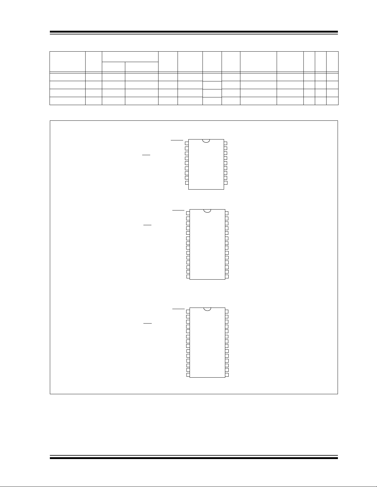
dsPIC30F Sensor Processor Family
Device Pins
Program Memory
Bytes Instructions
dsPIC30F2011 18 12K 4K 1024 0 3 2 2 8 ch 1 1 1
dsPIC30F3012 18 24K 8K 2048 1024 3 2 2 8 ch 1 1 1
dsPIC30F2012 28 12K 4K 1024 0 3 2 2 10 ch 1 1 1
dsPIC30F3013 28 24K 8K 2048 1024 3 2 2 10 ch 2 1 1
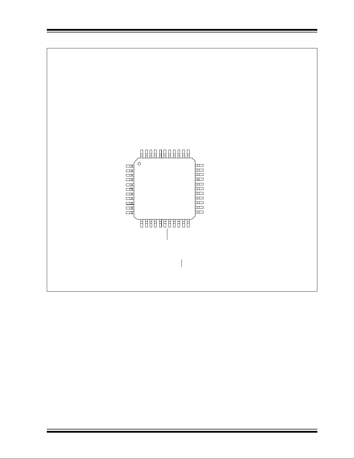
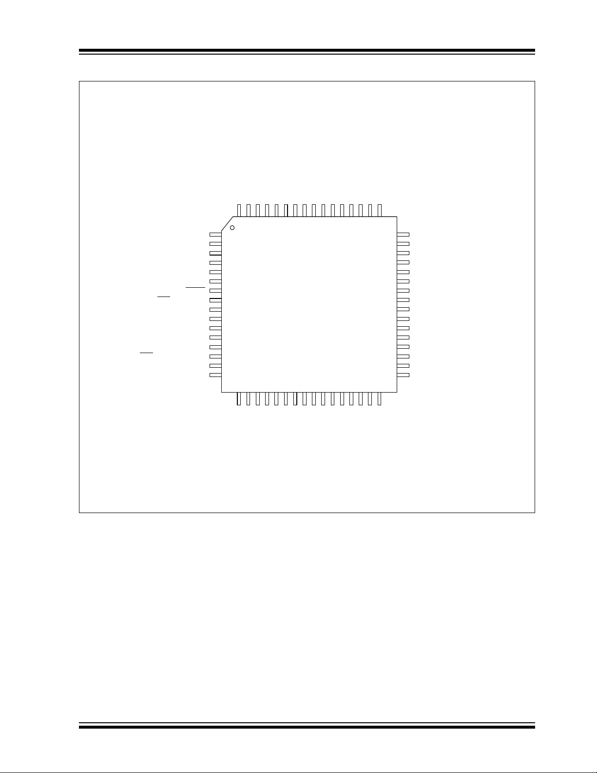
Pin Diagrams
18-Pin SOIC and PDIP
SRAM
Bytes
EEPROM
Bytes
Timer
16-bit
Input
Cap
Output Comp/
Std PWM
A/D 12-bit
100 Ksps
UART
™
SPI
C™
2
I
EMUD1/SOSCI/T2CK/U1ATX/CN1/RC13
EMUC1/SOSCO/T1CK/U1ARX/CN0/RC14
28-Pin PDIP and SOIC
EMUD3/AN0/VREF+/CN2/RB0
EMUC3/AN1/V
EMUD1/SOSCI/T2CK/U1ATX/CN1/RC13
EMUC1/SOSCO/T1CK/U1ARX/CN0/RC14
28-Pin PDIP and SOIC
EMUD3/AN0/VREF+/CN2/RB0
EMUC3/AN1/V
EMUD1/SOSCI/T2CK/U1ATX/CN1/RC13
EMUC1/SOSCO/T1CK/U1ARX/CN0/RC14
AN0/VREF+/CN2/RB0
AN1/V
AN2/SS1
/LVDIN/CN4/RB2
OSC2/CLKO/RC15
AN2/SS1/LVDIN/CN4/RB2
OSC2/CLKO/RC15
/LVDIN/CN4/RB2
AN2/SS1
OSC2/CLKO/RC15
MCLR
REF-/CN3/RB1
AN3/CN5/RB3
OSC1/CLKI
MCLR
REF-/CN3/RB1
AN3/CN5/RB3
AN4/CN6/RB4
AN5/CN7/RB5
OSC1/CLKI
IC2/INT2/RD9
MCLR
REF-/CN3/RB1
AN3/CN5/RB3
AN4/CN6/RB4
AN5/CN7/RB5
OSC1/CLKI
IC2/INT2/RD9
VSS
VDD
VSS
VDD
1
dsPIC30F2011
dsPIC30F3012
2
3
4
5
6
7
8
9
1
2
3
dsPIC30F2012
4
5
6
7
8
9
10
11
12
13
14
1
2
3
4
dsPIC30F3013
5
6
7
8
9
10
11
12
13
14
18
AV
DD
17
AVSS
16
AN6/SCK1/INT0/OCFA/RB6
15
EMUD2/AN7/OC2/IC2/INT2/RB7
14
VDD
13
V
SS
12
PGC/EMUC/AN5/U1RX/SDI1/SDA/CN7/RB5
11
PGD/EMUD/AN4/U1TX/SDO1/SCL/CN6/RB4
10
EMUC2/OC1/IC1/INT1/RD0
28
DD
AV
AVSS
27
AN6/OCFA/RB6
26
EMUD2/AN7/RB7
25
AN8/OC1/RB8
24
AN9/OC2/RB9
23
CN17/RF4
22
CN18/RF5
21
V
DD
20
SS
V
19
PGC/EMUC/U1RX/SDI1/SDA/RF2
18
PGD/EMUD/U1TX/SDO1/SCL/RF3
17
SCK1/INT0/RF6
16
EMUC2/IC1/INT1/RD8
15
28
AVDD
27
AVSS
AN6/OCFA/RB6
26
EMUD2/AN7/RB7
25
24
AN8/OC1/RB8
AN9/OC2/RB9
23
U2RX/CN17/RF4
22
21
U2TX/CN18/RF5
VDD
20
19
SS
V
PGC/EMUC/U1RX/SDI1/SDA/RF2
18
PGD/EMUD/U1TX/SDO1/SCL/RF3
17
16
SCK1/INT0/RF6
15
EMUC2/IC1/INT1/RD8
Note: For descriptions of individual pins, see Section 1.0.
2004 Microchip Technology Inc. Preliminary DS70083G-page 3
Page 6
dsPIC30F
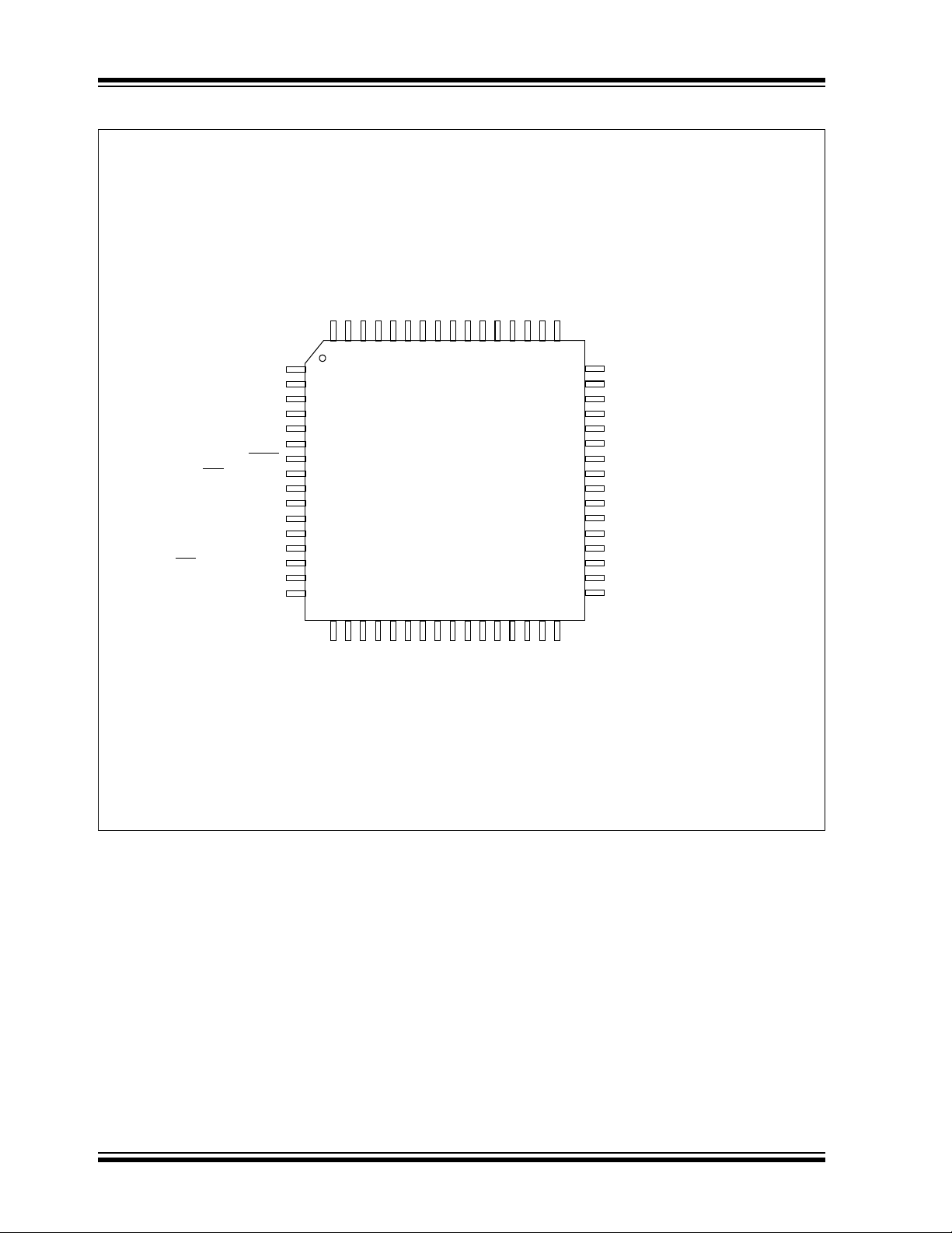
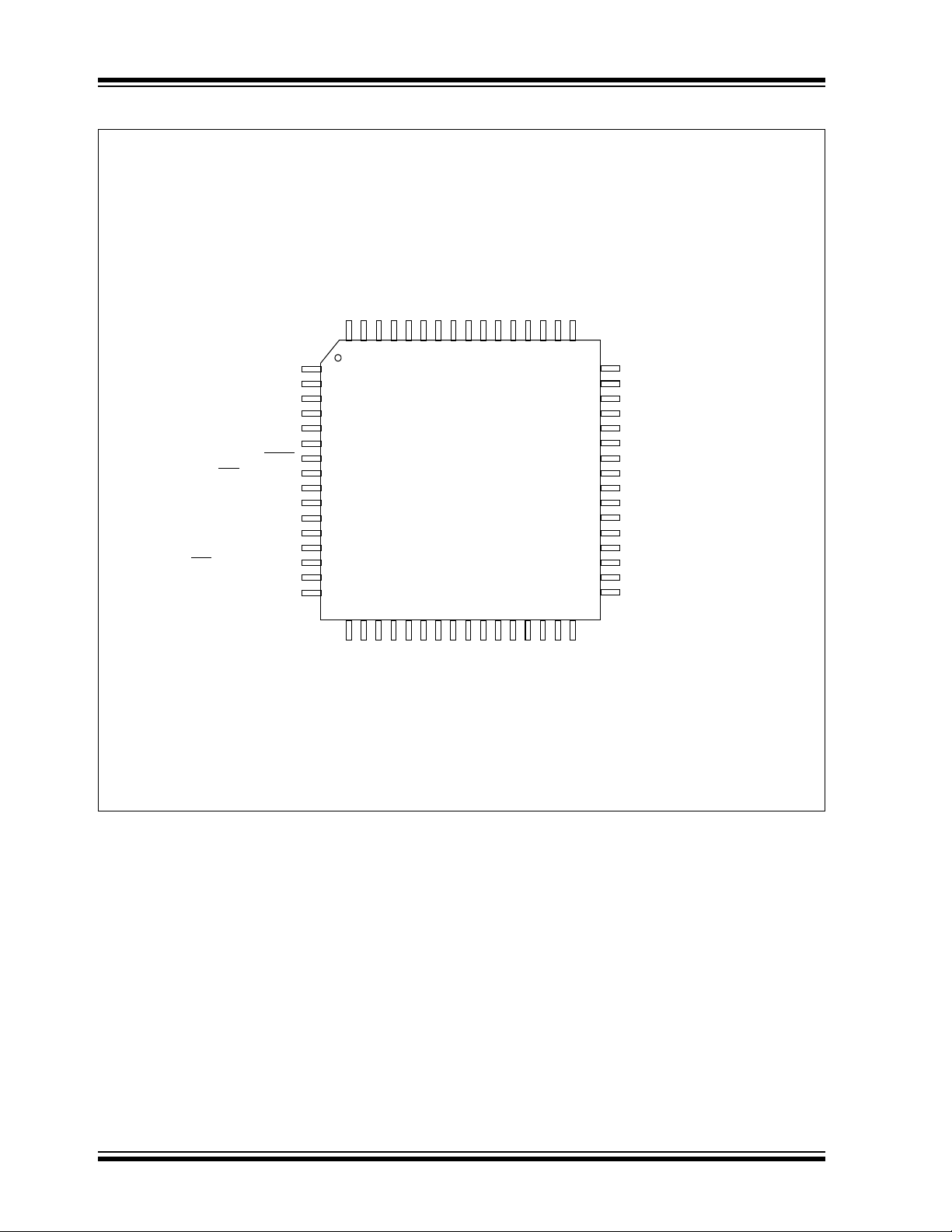
Pin Diagrams (Continued)
44-Pin QFN
PGD/EMUD/U1TX/SDO1/SCL/RF3
SCK1/INT0/RF6
NC
EMUC2/IC1/INT1/RD8
NC
NC
DD
EMUD1/SOSCI/T2CK / U1ATX / CN1 / RC13
EMUC1/SOSCO/T1CK / U1ARX / CN0 / RC14
NC
IC2/INT2/RD9
V
444342414039383736
PGC/EMUC/U1RX/SDI1/SDA/RF2
U2TX/CN18/RF5
U2RX/CN17/RF4
AN9/OC2/RB9
AN8/OC1/RB8
1
2 32
SS
V
3
NC
4
DD
V
5
NC
NC
NC
6
7
8
9
10
11
dsPIC30F3013
121314151617181920
NC
NC
AVSS
AN6/OCFA/RB6
EMUD2/AN7/RB7
Note: For descriptions of individual pins, see Section 1.0.
AVDD
MCLR
35
34
22
21
NC
REF-/CN3/RB1
REF+/CN2/RB0
EMUC3/AN1/V
EMUD3/AN0/V
33
OSC2/CLKO/RC15
OSC1/CLKI
VSS
31
30
SS
V
29
NC
NC
28
AN5/CN7/RB5
27
AN4/CN6/RB4
26
AN3/CN5/RB3
25
24
NC
23
AN2/SS1/LVDIN/CN4/RB2
NC
DS70083G-page 4 Preliminary 2004 Microchip Technology Inc.
Page 7
dsPIC30F
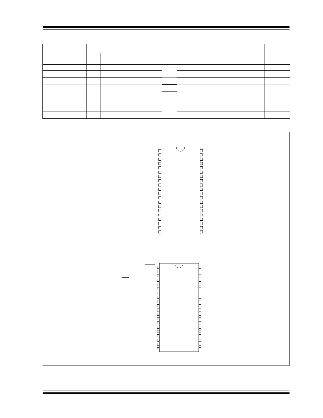
dsPIC30F General Purpose Controller Family
Program Memory
Device Pins
Bytes Instructions
SRAM
Bytes
EEPROM
Bytes
Timer
16-bit
dsPIC30F3014 40/44 24K 8K 2048 1024 3 2 2 — 13 ch 2 1 1 -
dsPIC30F4013 40/44 48K 16K 2048 1024 5 4 4 AC’97, I
dsPIC30F5011 64 66K 22K 4096 1024 5 8 8 AC’97, I
dsPIC30F6011 64 132K 44K 6144 2048 5 8 8 — 16 ch 2 2 1 2
dsPIC30F6012 64 144K 48K 8192 4096 5 8 8 AC’97, I
dsPIC30F5013 80 66K 22K 4096 1024 5 8 8 AC’97, I
dsPIC30F6013 80 132K 44K 6144 2048 5 8 8 — 16 ch 2 2 1 2
dsPIC30F6014 80 144K 48K 8192 4096 5 8 8 AC’97, I
Pin Diagrams
40-Pin PDIP
Input
Cap
Output
Comp/Std
PWM
Codec
Interface
A/D 12-bit
100 Ksps
2
S 13 ch 2 1 1 1
2
S 16 ch 2 2 1 2
2
S 16 ch 2 2 1 2
2
S 16 ch 2 2 1 2
2
S 16 ch 2 2 1 2
UART
™
SPI
C™
2
I
CAN
AN0/V
AN1/V
AN2/SS1
PGC/EMUC/AN6/OCFA/RB6
PGD/EMUD/AN7/RB7
EMUD1/SOSCI/T2CK/U1ATX/CN1/RC13
EMUC1/SOSCO/T1CK/U1ARX/CN0/RC14
OSC2/CLKO/RC15
40-Pin PDIP
AN0/V
AN1/V
AN2/SS1
/LVDIN/CN4/RB2
AN4/IC7/CN6/RB4
AN5/IC8/CN7/RB5
PGC/EMUC/AN6/OCFA/RB6
PGD/EMUD/AN7/RB7
EMUD1/SOSCI/T2CK/U1ATX/CN1/RC13
EMUC1/SOSCO/T1CK/U1ARX/CN0/RC14
OSC2/CLKO/RC15
MCLR
REF
+/CN2/RB0
REF
-/CN3/RB1
/LVDIN/CN4/RB2
AN3/CN5/RB3
AN4/CN6/RB4
AN5/CN7/RB5
AN8/RB8
V
DD
V
SS
OSC1/CLKI
INT0/RA11
IC2/INT2/RD9
RD3
V
SS
MCLR
REF
+/CN2/RB0
REF
-/CN3/RB1
AN3/CN5/RB3
AN8/RB8
V
DD
V
SS
OSC1/CLKI
INT0/RA11
IC2/INT2/RD9
OC4/RD3
V
SS
AV
1
2
3
4
5
6
7
8
9
10
11
12
13
14
15
16
17
18
19
20
1
2
3
4
5
6
7
8
9
10
11
12
13
14
15
16
17
18
19
20
dsPIC30F3014
40
39
38
37
36
35
dsPIC30F4013
34
33
32
31
30
29
28
27
26
25
24
23
22
21
DD
40
AV
SS
39
AN9/RB9
38
AN10/RB10
37
AN11/RB11
36
AN12/RB12
35
EMUC2/OC1/RD0
34
EMUD2/OC2/RD1
33
V
DD
32
SS
V
31
RF0
30
RF1
29
28
U2RX/CN17/RF4
U2TX/CN18/RF5
27
U1RX/SDI1/SDA/RF2
26
EMUD3/U1TX/SDO1/SCL/RF3
25
EMUC3/SCK1/RF6
24
IC1/INT1/RD8
23
RD2
22
V
DD
21
DD
AV
AV
SS
AN9/CSCK/RB9
AN10/CSDI/RB10
AN11/CSDO/RB11
AN12/COFS/RB12
EMUC2/OC1/RD0
EMUD2/OC2/RD1
V
DD
V
SS
C1RX/RF0
C1TX/RF1
U2RX/CN17/RF4
U2TX/CN18/RF5
U1RX/SDI1/SDA/RF2
EMUD3/U1TX/SDO1/SCL/RF3
EMUC3/SCK1/RF6
IC1/INT1/RD8
OC3/RD2
V
DD
Note: For descriptions of individual pins, see Section 1.0.
2004 Microchip Technology Inc. Preliminary DS70083G-page 5
Page 8
dsPIC30F
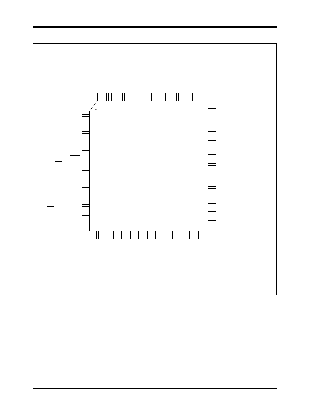
Pin Diagrams (Continued)
44-Pin TQFP
DD
EMUC3/SCK1/RF6
INT1/RD8
RD2
V
VSSRD3
IC2/INT2/RD1
38
39
37
dsPIC30F3014
1819202122
15
16
17
NC
DD
AVSS
AV
AN9/RB9
AN10/RB10
MCLR
REF+/CN2/RB0
AN0/V
EMUC1/SOSCO/T1CK/U1ARX/CN0/RC14
INT0/RA11
363435
REF-/CN3/RB1
/LVDIN/CN4/RB2
AN1/V
AN2/SS1
U1RX/SDI1/SDA/RF2
U2TX/CN18/RF5
U2RX/CN17/RF4
C1TX/RF1
C1RX/RF0
VSS
EMUD2/OC2/RD1
EMUC2/OC1/RD0
V
AN12/RB12
AN11/RB11
DD
EMUD3/U1TX/SDO1/SCL/RF3
4443424140
1
2
3
4
5
6
7
8
9
10
11
121314
NC
Note: For descriptions of individual pins, see Section 1.0.
NC
NC
33
EMUD1/SOSCI/T2CK/U1ATX/CN1/RC13
32
OSC2/CLKO/RC15
31
OSC1/CLKI
30
VSS
29
28
27
26
25
24
23
AN3/CN5/RB3
DD
V
AN8/RB8
PGD/EMUD/AN7/RB7
PGC/EMUC/AN6/OCFA/RB6
AN5/CN7/RB5
AN4/CN6/RB4
DS70083G-page 6 Preliminary 2004 Microchip Technology Inc.
Page 9
Pin Diagrams (Continued)
44-Pin TQFP
dsPIC30F
DD
EMUC3/SCK1/RF6
IC1/INT1/RD8
OC3/RD2
V
VSSOC4/RD3
IC2/INT2/RD1
38
39
37
1819202122
15
16
17
NC
DD
AVSS
AV
MCLR
AN9/CSCK/RB9
AN10/CSDI/RB10
REF+/CN2/RB0
AN0/V
EMUC1/SOSCO/T1CK/U1ARX/CN0/RC14
INT0/RA11
363435
REF-/CN3/RB1
/LVDIN/CN4/RB2
AN1/V
AN2/SS1
U1RX/SDI1/SDA/RF2
U2TX/CN18/RF5
U2RX/CN17/RF4
CTX1/RF1
CRX1/RF0
VSS
V
EMUD2/OC2/RD1
EMUC2/OC1/RD0
AN12/COFS/RB12
AN11/CSDO/RB11
DD
EMUD3/U1TX/SDO1/SCL/RF3
4443424140
1
2
3
4
5
dsPIC30F4013
6
7
8
9
10
11
121314
NC
Note: For descriptions of individual pins, see Section 1.0.
NC
NC
33
EMUD1/SOSCI/T2CK/U1ATX/CN1/RC13
32
OSC2/CLKO/RC15
31
OSC1/CLKI
30
VSS
29
V
28
27
26
25
24
23
AN3/CN5/RB3
DD
AN8/RB8
PGD/EMUD/TB7/AN7/RB7
PGC/EMUC/TB6/AN6/OCFA/RB6
AN5/IC8/CN7/RB5
AN4/IC7/CN6/RB4
2004 Microchip Technology Inc. Preliminary DS70083G-page 7
Page 10
dsPIC30F
Pin Diagrams (Continued)
44-Pin QFN
U1RX/SDI1/SDA/RF2
U2TX/CN18/RF5
U2RX/CN17/RF4
C1TX/RF1
C1RX/RF0
EMUD2/OC2/RD1
EMUC2/OC1/RD0
AN12/RB12
EMUD3/U1TX/SDO1/SCL/RF3
44
1
2 32
3
4
5
6
VSS
7
VDD
8
DD
V
9
10
11
121314151617181920
DD
EMUC3/SCK1/RF6
IC1/INT1/RD8
RD2
V
434241403938373635
dsPIC30F3014
SS
RD3
V
EMUC1/SOSCO/T1CK/U1ARX/CN0/RC14
EMUD1/SOSCI/T2CK/U1ATX/CN1/RC13
IC2/INT2/RD9
INT0/RA11
34
33
OSC2/CLKO/RC15
OSC1/CLKI
31
VSS
30
VSS
29
VDD
28
V
DD
AN8/RB8
27
PGD/EMUD/AN7/RB7
26
PGC/EMUC/AN6/OCFA/RB6
25
AN5/CN7/RB5
24
AN4/CN6/RB4
23
21
22
NC
AN11/RB11
DD
AVSS
AV
AN9/RB9
AN10/RB10
Note: For descriptions of individual pins, see Section 1.0.
MCLR
REF-/CN3/RB1
REF+/CN2/RB0
AN1/V
AN0/V
AN3/CN5/RB3
S1/LVDIN/CN4/RB2
AN2/S
DS70083G-page 8 Preliminary 2004 Microchip Technology Inc.
Page 11
Pin Diagrams (Continued)
44-Pin QFN
dsPIC30F
DD
EMUC3/SCK1/RF6
INT1/RD8
TOC3/RD2
V
VSSOC4/RD3
dsPIC30F4013
NC
DD
AVSS
AV
MCLR
AN9/CSCK/RB9
AN10/CSDI/RB10
IC2/INT2/RD1
REF+/CN2/RB0
AN0/V
U1RX/SDI1/SDA/RF2
U2TX/CN18/RF5
U2RX/CN17/RF4
CTX1/RF1
CRX1/RF0
VSS
VDD
DD
EMUD2/OC2/RD1
EMUC2/OC1/RD0
AN12/COFS/RB12
V
EMUD3/U1TX/SDO1/SCL/RF3
444342414039383736
1
2 32
3
4
5
6
7
8
9
10
11
121314151617181920
AN11/CSDO/RB11
Note: For descriptions of individual pins, see Section 1.0.
EMUC1/SOSCO/T1CK/U1ARX/CN0/RC14
EMUD1/SOSCI/T2CK/U1ATX/CN1/RC13
INT0/RA11
35
34
33
OSC2/CLKO/RC15
OSC1/CLKI
31
VSS
30
VSS
29
VDD
V
DD
28
AN8/RB8
27
PGD/EMUD/TB7/AN7/RB7
26
PGC/EMUC/TB6/AN6/OCFA/RB6
25
AN5/IC8/CN7/RB5
24
AN4/IC7/CN6/RB4
23
21
22
REF-/CN3/RB1
AN3/CN5/RB3
/LVDIN/CN4/RB2
AN1/V
AN2/SS1
2004 Microchip Technology Inc. Preliminary DS70083G-page 9
Page 12
dsPIC30F
Pin Diagrams (Continued)
64-Pin TQFP
AN5/IC8/CN7/RB5
AN4/IC7/CN6/RB4
AN2/SS1
AN1/V
AN0/V
COFS/RG15
T2CK/RC1
T3CK/RC2
SCK2/CN8/RG6
SDI2/CN9/RG7
SDO2/CN10/RG8
/LVDIN/CN4/RB2
MCLR
/CN11/RG9
SS2
AN3/CN5/RB3
REF-/CN3/RB1
REF+/CN2/RB0
VSS
VDD
CSDO/RG13
CSDI/RG12
CSCK/RG14
C2TX/RG1
C2RX/RG0
646362616059585756
1
2
3
4
5
6
7
8
9
10
11
12
13
14
15
16
171819202122232425
PGC/EMUC/AN6/OCFA/RB6
dsPIC30F5011
DD
AVSS
AV
AN8/RB8
PGD/EMUD/AN7/RB7
C1TX/RF1
VDD
C1RX/RF0
AN9/RB9
AN11/RB11
AN10/RB10
OC8/CN16/RD7
VSS
OC7/CN15/RD6
OC6/IC6/CN14/RD5
545352
55
28
27
26
SS
V
VDD
AN12/RB12
AN13/RB13
EMUD2/OC2/RD1
OC3/RD2
OC4/RD3
OC5/IC5/CN13/RD4
504951
48
47
46
45
44
43
42
41
40
39
38
37
36
35
34
33
32
31
30
29
AN14/RB14
U2TX/CN18/RF5
U2RX/CN17/RF4
AN15/OCFB/CN12/RB15
EMUC1/SOSCO/T1CK/CN0/RC14
EMUD1/SOSCI/T4CK/CN1/RC13
EMUC2/OC1/RD0
IC4/INT4/RD11
IC3/INT3/RD10
IC2/INT2/RD9
IC1/INT1/RD8
SS
V
OSC2/CLKO/RC15
OSC1/CLKI
DD
V
SCL/RG2
SDA/RG3
EMUC3/SCK1/INT0/RF6
U1RX/SDI1/RF2
EMUD3/U1TX/SDO1/RF3
Note: For descriptions of individual pins, see Section 1.0.
DS70083G-page 10 Preliminary 2004 Microchip Technology Inc.
Page 13
Pin Diagrams (Continued)
64-Pin TQFP
RG13
RG12
RG14
C2TX/RG1
C1TX/RF1
C2RX/RG0
SS
V
VDD
C1RX/RF0
OC8/CN16/RD7
OC4/RD3
OC7/CN15/RD6
OC6/IC6/CN14/RD5
OC5/IC5/CN13/RD4
EMUD2/OC2/RD1
OC3/RD2
dsPIC30F
SDO2/CN10/RG8
AN5/IC8/CN7/RB5
AN4/IC7/CN6/RB4
AN2/SS1
PGC/EMUC/AN1/V
PGD/EMUD/AN0/V
RG15
T2CK/RC1
T3CK/RC2
SCK2/CN8/RG6
SDI2/CN9/RG7
MCLR
SS2/CN11/RG9
VSS
VDD
AN3/CN5/RB3
/LVDIN/CN4/RB2
REF-/CN3/RB1
REF+/CN2/RB0
646362616059585756
1
2
3
4
5
6
7
8
9
10
11
12
13
14
15
16
171819202122232425
AN6/OCFA/RB6
DD
AVSS
AV
AN7/RB7
dsPIC30F6011
AN8/RB8
AN9/RB9
AN11/RB11
AN10/RB10
55
26
SS
V
VDD
545352
27
AN12/RB12
504951
31
30
29
28
AN13/RB13
AN14/RB14
U2RX/CN17/RF4
AN15/OCFB/CN12/RB15
EMUC1/SOSCO/T1CK/CN0/RC14
48
EMUD1/SOSCI/T4CK/CN1/RC13
47
EMUC2/OC1/RD0
46
45
IC4/INT4/RD11
IC3/INT3/RD10
44
43
IC2/INT2/RD9
42
IC1/INT1/RD8
SS
41
V
OSC2/CLKO/RC15
40
OSC1/CLKI
39
DD
V
38
SCL/RG2
37
SDA/RG3
36
EMUC3/SCK1/INT0/RF6
35
U1RX/SDI1/RF2
34
EMUD3/U1TX/SDO1/RF3
33
32
U2TX/CN18/RF5
Note: For descriptions of individual pins, see Section 1.0.
2004 Microchip Technology Inc. Preliminary DS70083G-page 11
Page 14
dsPIC30F
Pin Diagrams (Continued)
64-Pin TQFP
CSDO/RG13
CSDI/RG12
CSCK/RG14
C2RX/RG0
C2TX/RG1
C1TX/RF1
C1RX/RF0
SS
OC8/CN16/RD7
V
VDD
OC3/RD2
OC4/RD3
OC7/CN15/RD6
OC6/IC6/CN14/RD5
OC5/IC5/CN13/RD4
EMUD2/OC2/RD1
SDO2/CN10/RG8
AN5/IC8/CN7/RB5
AN4/IC7/CN6/RB4
AN2/SS1
PGC/EMUC/AN1/V
PGD/EMUD/AN0/V
COFS/RG15
T2CK/RC1
T3CK/RC2
SCK2/CN8/RG6
SDI2/CN9/RG7
MCLR
/CN11/RG9
SS2
AN3/CN5/RB3
/LVDIN/CN4/RB2
REF-/CN3/RB1
REF+/CN2/RB0
VSS
VDD
646362616059585756
1
2
3
4
5
6
7
8
9
10
11
12
13
14
15
16
171819202122232425
AN6/OCFA/RB6
DD
AVSS
AV
AN7/RB7
dsPIC30F6012
AN8/RB8
AN9/RB9
AN11/RB11
AN10/RB10
55
26
SS
V
VDD
545352
27
AN12/RB12
504951
31
30
29
28
AN13/RB13
AN14/RB14
U2RX/CN17/RF4
AN15/OCFB/CN12/RB15
48
47
46
45
44
43
42
41
40
39
38
37
36
35
34
33
32
U2TX/CN18/RF5
EMUC1/SOSCO/T1CK/CN0/RC14
EMUD1/SOSCI/T4CK/CN1/RC13
EMUC2/OC1/RD0
IC4/INT4/RD11
IC3/INT3/RD10
IC2/INT2/RD9
IC1/INT1/RD8
SS
V
OSC2/CLKO/RC15
OSC1/CLKI
DD
V
SCL/RG2
SDA/RG3
EMUC3/SCK1/INT0/RF6
U1RX/SDI1/RF2
EMUD3/U1TX/SDO1/RF3
Note: For descriptions of individual pins, see Section 1.0.
DS70083G-page 12 Preliminary 2004 Microchip Technology Inc.
Page 15

Pin Diagrams (Continued)
80-Pin TQFP
CSCK/RG14
CSDO/RG13
RA7/CN23
CSDI/RG12
RA6/CN22
C2RX/RG0
C2TX/RG1
C1TX/RF1
C1RX/RF0
DD
V
OC8/CN16/RD7
VSS
IC5/RD12
OC6/CN14/RD5
OC5/CN13/RD4
IC6/CN19/RD13
OC7/CN15/RD6
OC4/RD3
OC3/RD2
EMUD2/OC2/RD1
dsPIC30F
COFS/RG15
T2CK/RC1
T3CK/RC2
T4CK/RC3
T5CK/RC4
SCK2/CN8/RG6
SDI2/CN9/RG7
SDO2/CN10/RG8
MCLR
SS2/CN11/RG9
V
VDD
INT1/RA12
INT2/RA13
AN5/CN7/RB5
AN4/CN6/RB4
AN3/CN5/RB3
/LVDIN/CN4/RB2
AN2/SS1
PGC/EMUC/AN1/CN3/RB1
PGD/EMUD/AN0/CN2/RB0
80
79
1
2
3
4
5
6
7
8
9
10
SS
11
12
13
14
15
16
17
18
19
20
21
22
2324252627282930313233
REF-/RA9
AN7/RB7
V
AN6/OCFA/RB6
AVDD
VREF+/RA10
75
767877
AVSS
727473
7170696867666564636261
dsPIC30F5013
VSS
AN8/RB8
AN9/RB9
AN11/RB11
AN10/RB10
DD
V
AN12/RB12
36
35
34
AN13/RB13
AN14/RB14
60
59
58
57
56
55
54
53
52
51
50
49
48
47
46
45
44
43
42
41
40
39
38
37
IC7/CN20/RD14
IC8/CN21/RD15
U2TX/CN18/RF5
U2RX/CN17/RF4
EMUC1/SOSCO/T1CK/CN0/RC14
EMUD1/SOSCI/CN1/RC13
EMUC2/OC1/RD0
IC4/RD11
IC3/RD10
IC2/RD9
IC1/RD8
INT4/RA15
INT3/RA14
V
SS
OSC2/CLKO/RC15
OSC1/CLKI
DD
V
SCL/RG2
SDA/RG3
EMUC3/SCK1/INT0/RF6
SDI1/RF7
EMUD3/SDO1/RF8
U1RX/RF2
U1TX/RF3
AN15/OCFB/CN12/RB15
Note: For descriptions of individual pins, see Section 1.0.
2004 Microchip Technology Inc. Preliminary DS70083G-page 13
Page 16
dsPIC30F
Pin Diagrams (Continued)
80-Pin TQFP
DD
RG14
RA7/CN23
RA6/CN22
C2RX/RG0
RG13
RG12
C2TX/RG1
C1TX/RF1
C1RX/RF0
V
OC8/CN16/RD7
VSS
OC6/CN14/RD5
OC7/CN15/RD6
IC5/RD12
OC4/RD3
OC5/CN13/RD4
IC6/CN19/RD13
OC3/RD2
EMUD2/OC2/RD1
RG15
T2CK/RC1
T3CK/RC2
T4CK/RC3
T5CK/RC4
SCK2/CN8/RG6
SDI2/CN9/RG7
SDO2/CN10/RG8
MCLR
SS2/CN11/RG9
V
VDD
INT1/RA12
INT2/RA13
AN5/CN7/RB5
AN4/CN6/RB4
AN3/CN5/RB3
/LVDIN/CN4/RB2
AN2/SS1
PGC/EMUC/AN1/CN3/RB1
PGD/EMUD/AN0/CN2/RB0
80
79
1
2
3
4
5
6
7
8
9
10
SS
11
12
13
14
15
16
17
18
19
20
21
22
2324252627282930313233
AN7/RB7
VREF-/RA9
AN6/OCFA/RB6
DD
AV
VREF+/RA10
75
767877
AVSS
727473
7170696867666564636261
dsPIC30F6013
VSS
AN8/RB8
AN9/RB9
AN11/RB11
AN10/RB10
DD
V
AN12/RB12
36
35
34
AN13/RB13
AN14/RB14
60
59
58
57
56
55
54
53
52
51
50
49
48
47
46
45
44
43
42
41
40
39
38
37
IC8/CN21/RD15
IC7/CN20/RD14
U2TX/CN18/RF5
U2RX/CN17/RF4
EMUC1/SOSCO/T1CK/CN0/RC14
EMUD1/SOSCI/CN1/RC13
EMUC2/OC1/RD0
IC4/RD11
IC3/RD10
IC2/RD9
IC1/RD8
INT4/RA15
INT3/RA14
SS
V
OSC2/CLKO/RC15
OSC1/CLKI
DD
V
SCL/RG2
SDA/RG3
EMUC3/SCK1/INT0/RF6
SDI1/RF7
EMUD3/SDO1/RF8
U1RX/RF2
U1TX/RF3
AN15/OCFB/CN12/RB15
Note: For descriptions of individual pins, see Section 1.0.
DS70083G-page 14 Preliminary 2004 Microchip Technology Inc.
Page 17

Pin Diagrams (Continued)
80-Pin TQFP
CSCK/RG14
CSDO/RG13
RA7/CN23
CSDI/RG12
RA6/CN22
C2RX/RG0
C2TX/RG1
C1TX/RF1
C1RX/RF0
DD
V
OC8/CN16/RD7
VSS
IC5/RD12
OC6/CN14/RD5
OC5/CN13/RD4
IC6/CN19/RD13
OC7/CN15/RD6
OC4/RD3
OC3/RD2
EMUD2/OC2/RD1
dsPIC30F
COFS/RG15
T2CK/RC1
T3CK/RC2
T4CK/RC3
T5CK/RC4
SCK2/CN8/RG6
SDI2/CN9/RG7
SDO2/CN10/RG8
MCLR
SS2/CN11/RG9
V
VDD
INT1/RA12
INT2/RA13
AN5/CN7/RB5
AN4/CN6/RB4
AN3/CN5/RB3
/LVDIN/CN4/RB2
AN2/SS1
PGC/EMUC/AN1/CN3/RB1
PGD/EMUD/AN0/CN2/RB0
80
79
1
2
3
4
5
6
7
8
9
10
SS
11
12
13
14
15
16
17
18
19
20
21
22
2324252627282930313233
REF-/RA9
AN7/RB7
V
AN6/OCFA/RB6
AVDD
VREF+/RA10
75
767877
AVSS
727473
7170696867666564636261
dsPIC30F6014
VSS
AN8/RB8
AN9/RB9
AN11/RB11
AN10/RB10
DD
V
AN12/RB12
36
35
34
AN13/RB13
AN14/RB14
60
59
58
57
56
55
54
53
52
51
50
49
48
47
46
45
44
43
42
41
40
39
38
37
IC7/CN20/RD14
IC8/CN21/RD15
U2TX/CN18/RF5
U2RX/CN17/RF4
EMUC1/SOSCO/T1CK/CN0/RC14
EMUD1/SOSCI/CN1/RC13
EMUC2/OC1/RD0
IC4/RD11
IC3/RD10
IC2/RD9
IC1/RD8
INT4/RA15
INT3/RA14
V
SS
OSC2/CLKO/RC15
OSC1/CLKI
DD
V
SCL/RG2
SDA/RG3
EMUC3/SCK1/INT0/RF6
SDI1/RF7
EMUD3/SDO1/RF8
U1RX/RF2
U1TX/RF3
AN15/OCFB/CN12/RB15
Note: For descriptions of individual pins, see Section 1.0.
2004 Microchip Technology Inc. Preliminary DS70083G-page 15
Page 18

dsPIC30F
Table of Contents
1.0 Device Overview ........................................................................................................................................................................ 17
2.0 CPU Architecture Overview........................................................................................................................................................ 21
3.0 Memory Organization ................................................................................................................................................................. 35
4.0 Address Generator Units............................................................................................................................................................ 47
5.0 Interrupts .................................................................................................................................................................................... 55
6.0 Flash Program Memory.............................................................................................................................................................. 63
7.0 Data EEPROM Memory ............................................................................................................................................................. 69
8.0 I/O Ports ..................................................................................................................................................................................... 75
9.0 Timer1 Module ........................................................................................................................................................................... 81
10.0 Timer2/3 Module ........................................................................................................................................................................ 85
11.0 Timer4/5 Module ....................................................................................................................................................................... 91
12.0 Input Capture Module ................................................................................................................................................................. 95
13.0 Output Compare Module ............................................................................................................................................................ 99
14.0 SPI Module ............................................................................................................................................................................... 103
15.0 I2C Module ............................................................................................................................................................................... 107
16.0 Universal Asynchronous Receiver Transmitter (UART) Module .............................................................................................. 115
17.0 CAN Module ............................................................................................................................................................................. 123
18.0 Data Converter Interface (DCI) Module.................................................................................................................................... 135
19.0 12-bit Analog-to-Digital Converter (A/D) Module ...................................................................................................................... 145
20.0 System Integration ................................................................................................................................................................... 153
21.0 Instruction Set Summary .......................................................................................................................................................... 169
22.0 Development Support............................................................................................................................................................... 177
23.0 Electrical Characteristics .......................................................................................................................................................... 183
24.0 Packaging Information.............................................................................................................................................................. 223
Index .................................................................................................................................................................................................. 237
On-Line Support................................................................................................................................................................................. 243
Systems Information and Upgrade Hot Line ...................................................................................................................................... 243
Reader Response .............................................................................................................................................................................. 244
Product Identification System............................................................................................................................................................. 245
TO OUR VALUED CUSTOMERS
It is our intention to provide our valued customers with the best documentation possible to ensure successful use of your Microchip
products. To this end, we will continue to improve our publications to better suit your needs. Our publications will be refined and
enhanced as new volumes and updates are introduced.
If you have any questions or comments regarding this publication, please contact the Marketing Communications Department via
E-mail at docerrors@mail.microchip.com or fax the Reader Response Form in the back of this data sheet to (480) 792-4150.
We welcome your feedback.
Most Current Data Sheet
To obtain the most up-to-date version of this data sheet, please register at our Worldwide Web site at:
http://www.microchip.com
You can determine the version of a data sheet by examining its literature number found on the bottom outside corner of any page.
The last character of the literature number is the version number, (e.g., DS30000A is version A of document DS30000).
Errata
An errata sheet, describing minor operational differences from the data sheet and recommended workarounds, may exist for current
devices. As device/documentation issues become known to us, we will publish an errata sheet. The errata will specify the revision
of silicon and revision of document to which it applies.
To determine if an errata sheet exists for a particular device, please check with one of the following:
• Microchip’s Worldwide Web site; http://www.microchip.com
• Your local Microchip sales office (see last page)
• The Microchip Corporate Literature Center; U.S. FAX: (480) 792-7277
When contacting a sales office or the literature center, please specify which device, revision of silicon and data sheet (include
literature number) you are using.
Customer Notification System
Register on our web site at www.microchip.com/cn to receive the most current information on all of our products.
DS70083G-page 16 Preliminary 2004 Microchip Technology Inc.
Page 19

dsPIC30F
1.0 DEVICE OVERVIEW
Note: This data sheet summarizes features of this group
of dsPIC30F devices and is not intended to be a complete
reference source. For more information on the CPU,
peripherals, register descriptions and general device
functionality, refer to the dsPIC30F Family Reference
Manual (DS70046). For more information on the device
instruction set and programming, refer to the dsPIC30F
Programmer’s Reference Manual (DS70030).
This document contains device family specific
information for the dsPIC30F family of Digital Signal
Controller (DSC) devices. The dsPIC30F devices
contain extensive Digital Signal Processor (DSP)
functionality within a high performance 16-bit
microcontroller (MCU) architecture.
Figure 1-1 shows a sample device block diagram.
Note: The device(s) depicted in this block
diagram are representative of the
corresponding device family. Other
devices of the same family may vary in
terms of number of pins and multiplexing
of pin functions. Typically, smaller devices
in the family contain a subset of the
peripherals present in the device(s) shown
in this diagram.
2004 Microchip Technology Inc. Preliminary DS70083G-page 17
Page 20
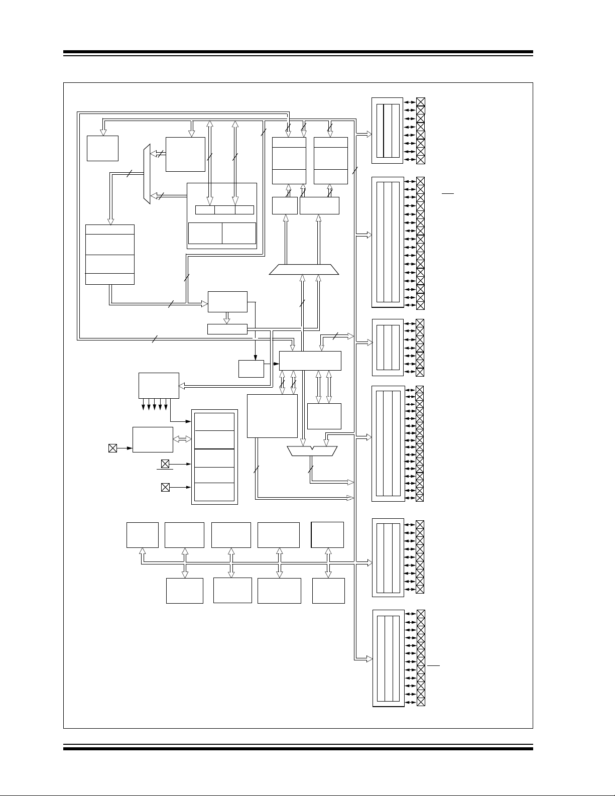
dsPIC30F
FIGURE 1-1: dsPIC30F5013/6013/6014 BLOCK DIAGRAM
Interrupt
Controller
Address Latch
Program Memory
(144 Kbytes)
Data EEPROM
(4 Kbytes)
Data Latch
Control Signals
to Various Blocks
OSC1/CLKI
24
Generation
24
24
16
Instruction
Decode &
Control
Timing
MCLR
VDD, V
AV
DD
, AV
PSV & Table
Data Access
Control Block
Stac k
Control
16
24
Start-up Timer
Low Voltage
SS
SS
Y Data Bus
16
8
PCH PCL
PCU
Program Counter
Logic
Power-up
Oscillator
POR/BOR
Watchdog
ROM Latch
IR
Timer
Reset
Timer
Detect
Loop
Control
Logic
Decode
16
Y AGU
DSP
Engine
16
X Data Bus
16
16
Y Data
RAM
(4 Kbytes)
Address
Latch
16
16
X RAGU
X WAGU
Effective Address
16
16 x 16
W Reg Array
16
16
ALU<16>
16
16
Data LatchData Latch
X Data
RAM
(4 Kbytes)
Address
Latch
16
16
Divide
Unit
16
PORTA
PORTB
PORTC
PORTD
CN22/RA6
CN23/RA7
V
REF
-/RA9
V
REF
+/RA10
INT1/RA12
INT2/RA13
INT3/RA14
INT4/RA15
PGD/EMUD/AN0/CN2/RB0
PGC/EMUC/AN1/CN3/RB1
AN2/SS1/LVDIN/CN4/RB2
AN3/CN5/RB3
AN4/CN6/RB4
AN5/CN7/RB5
AN6/OCFA/RB6
AN7/RB7
AN8/RB8
AN9/RB9
AN10/RB10
AN11/RB11
AN12/RB12
AN13/RB13
AN14/RB14
AN15/OCFB/CN12/RB15
T2CK/RC1
T3CK/RC2
T4CK/RC3
T5CK/RC4
EMUD1/SOSCI/CN1/RC13
EMUC1/SOSCO/T1CK/CN0/RC14
OSC2/CLKO/RC15
EMUC2/OC1/RD0
EMUD2/OC2/RD1
OC3/RD2
OC4/RD3
OC5/CN13/RD4
OC6/CN14/RD5
OC7/CN15/RD6
OC8/CN16/RD7
IC1/RD8
IC2/RD9
IC3/RD10
IC4/RD11
IC5/RD12
IC6/CN19/RD13
IC7/CN20/RD14
IC8/CN21/RD15
CAN1,
CAN2
12-bit ADC
Timers
Input
Capture
Module
DCI
Output
Compare
Module
SPI1,
SPI2
I2C
UART1,
UART2
PORTF
PORTG
C1RX/RF0
C1TX/RF1
U1RX/RF2
U1TX/RF3
U2RX/CN17/RF4
U2TX/CN18/RF5
EMUC3/SCK1/INT0/RF6
SDI1/RF7
EMUD3/SDO1/RF8
C2RX/RG0
C2TX/RG1
SCL/RG2
SDA/RG3
SCK2/CN8/RG6
SDI2/CN9/RG7
SDO2/CN10/RG8
/CN11/RG9
SS2
CSDI/RG12
CSDO/RG13
CSCK/RG14
COFS/RG15
DS70083G-page 18 Preliminary 2004 Microchip Technology Inc.
Page 21

dsPIC30F
Table 1-1 provides a brief description of device I/O
pinouts and the functions that may be multiplexed to a
port pin. Multiple functions may exist on one port pin.
When multiplexing occurs, the peripheral module’s
functional requirements may force an override of the
data direction of the port pin.
TABLE 1-1: PINOUT I/O DESCRIPTIONS
Pin Name
AN0-AN15 I Analog Analog input channels.
AV
DD P P Positive supply for analog module.
SS P P Ground reference for analog module.
AV
CLKI
CLKO
CN0-CN23 I ST Input change notification inputs.
COFS
CSCK
CSDI
CSDO
C1RX
C1TX
C2RX
C2TX
EMUD
EMUC
EMUD1
EMUC1
EMUD2
EMUC2
EMUD3
EMUC3
IC1-IC8 I ST Capture inputs 1 through 8.
INT0
INT1
INT2
INT3
INT4
LVDIN I Analog Low Voltage Detect Reference Voltage input pin.
MCLR
OCFA
OCFB
OC1-OC8
Pin
Typ e
I
O
I/O
I/O
I
O
I
O
I
O
I/O
I/O
I/O
I/O
I/O
I/O
I/O
I/O
I
I
I
I
I
I/P ST Master Clear (Reset) input or programming voltage input. This
I
I
O
Legend: CMOS = CMOS compatible input or output Analog = Analog input
ST = Schmitt Trigger input with CMOS levels O = Output
I = Input P = Power
Buffer
Typ e
AN0 and AN1 are also used for device programming data and
clock inputs, respectively.
ST/CMOS—External clock source input. Always associated with OSC1 pin
function.
Oscillator crystal output. Connects to crystal or resonator in
Crystal Oscillator mode. Optionally functions as CLKO in RC
and EC modes. Always associated with OSC2 pin
function.
Can be software programmed for internal weak pull-ups on all
inputs.
ST
ST
ST
—
ST
—
ST
—
ST
ST
ST
ST
ST
ST
ST
ST
ST
ST
ST
ST
ST
ST
ST
—
Data Converter Interface frame synchronization pin.
Data Converter Interface serial clock input/output pin.
Data Converter Interface serial data input pin.
Data Converter Interface serial data output pin.
CAN1 bus receive pin.
CAN1 bus transmit pin.
CAN2 bus receive pin.
CAN2 bus transmit pin
ICD Primary Communication Channel data input/output pin.
ICD Primary Communication Channel clock input/output pin.
ICD Secondary Communication Channel data
input/output pin.
ICD Secondary Communication Channel clock input/output pin.
ICD Tertiary Communication Channel data input/output pin.
ICD Tertiary Communication Channel clock input/output pin.
ICD Quaternary Communication Channel data
input/output pin.
ICD Quaternary Communication Channel clock input/output pin.
External interrupt 0.
External interrupt 1.
External interrupt 2.
External interrupt 3.
External interrupt 4.
pin is an active low Reset to the device.
Compare Fault A input (for Compare channels 1, 2, 3 and 4).
Compare Fault B input (for Compare channels 5, 6, 7 and 8).
Compare outputs 1 through 8.
Description
2004 Microchip Technology Inc. Preliminary DS70083G-page 19
Page 22

dsPIC30F
TABLE 1-1: PINOUT I/O DESCRIPTIONS (CONTINUED)
Pin Name
OSC1
OSC2
PGD
PGC
RA6-RA7
RA9-RA10
RA12-RA15
RB0-RB15 I/O ST PORTB is a bidirectional I/O port.
RC1-RC4
RC13-RC15
RD0-RD15 I/O ST PORTD is a bidirectional I/O port.
RF0-RF8 I/O ST PORTF is a bidirectional I/O port.
RG0-RG3
RG6-RG9
RG12-RG15
SCK1
SDI1
SDO1
SS1
SCK2
SDI2
SDO2
SS2
SCL
SDA
SOSCO
SOSCI
T1CK
T2CK
T3CK
T4CK
T5CK
U1RX
U1TX
U1ARX
U1ATX
U2RX
U2TX
DD P — Positive supply for logic and I/O pins.
V
SS P — Ground reference for logic and I/O pins.
V
V
REF+ I Analog Analog Voltage Reference (High) input.
REF- I Analog Analog Voltage Reference (Low) input.
V
Pin
Typ e
I
I/O
I/O
I
I/O
I/O
I/O
I/O
I/O
I/O
I/O
I/O
I/O
I
O
I
I/O
I
O
I
I/O
I/O
O
I
I
I
I
I
I
I
O
I
O
I
O
Legend: CMOS = CMOS compatible input or output Analog = Analog input
ST = Schmitt Trigger input with CMOS levels O = Output
I = Input P = Power
Buffer
Typ e
ST/CMOS—Oscillator crystal input. ST buffer when configured in RC mode;
CMOS otherwise.
Oscillator crystal output. Connects to crystal or resonator in
Crystal Oscillator mode. Optionally functions as CLKO in RC
and EC modes.
ST
ST
ST
ST
ST
ST
ST
ST
ST
ST
ST
ST
—
ST
ST
ST
—
ST
ST
ST
—
ST/CMOS
ST
ST
ST
ST
ST
ST
—
ST
—
ST
—
In-Circuit Serial Programming data input/output pin.
In-Circuit Serial Programming clock input pin.
PORTA is a bidirectional I/O port.
PORTC is a bidirectional I/O port.
PORTG is a bidirectional I/O port.
Synchronous serial clock input/output for SPI1.
SPI1 Data In.
SPI1 Data Out.
SPI1 Slave Synchronization.
Synchronous serial clock input/output for SPI2.
SPI2 Data In.
SPI2 Data Out.
SPI2 Slave Synchronization.
Synchronous serial clock input/output for I
Synchronous serial data input/output for I
32 kHz low power oscillator crystal output.
32 kHz low power oscillator crystal input. ST buffer when configured in RC mode; CMOS otherwise.
Timer1 external clock input.
Timer2 external clock input.
Timer3 external clock input.
Timer4 external clock input.
Timer5 external clock input.
UART1 Receive.
UART1 Transmit.
UART1 Alternate Receive.
UART1 Alternate Transmit.
UART2 Receive.
UART2 Transmit.
Description
2
C.
2
C.
DS70083G-page 20 Preliminary 2004 Microchip Technology Inc.
Page 23

dsPIC30F
2.0 CPU ARCHITECTURE OVERVIEW
Note: This data sheet summarizes features of this group
of dsPIC30F devices and is not intended to be a complete
reference source. For more information on the CPU,
peripherals, register descriptions and general device
functionality, refer to the dsPIC30F Family Reference
Manual (DS70046). For more information on the device
instruction set and programming, refer to the dsPIC30F
Programmer’s Reference Manual (DS70030).
2.1 Core Overview
The core has a 24-bit instruction word. The Program
Counter (PC) is 23-bits wide with the Least Significant
(LS) bit always clear (refer to Section 3.1), and the
Most Significant (MS) bit is ignored during normal program execution, except for certain specialized instructions. Thus, the PC can address up to 4M instruction
words of user program space. An instruction pre-fetch
mechanism is used to help maintain throughput. Program loop constructs, free from loop count management overhead, are supported using the DO and
REPEAT instructions, both of which are interruptible at
any point.
The working register array consists of 16 x 16-bit registers, each of which can act as data, address or offset
registers. One working register (W15) operates as a
software stack pointer for interrupts and calls.
The data space is 64 Kbytes (32K words) and is split
into two blocks, referred to as X and Y data memory.
Each block has its own independent Address Generation Unit (AGU). Most instructions operate solely
through the X memory, AGU, which provides the
appearance of a single unified data space. The
Multiply-Accumulate (MAC) class of dual source DSP
instructions operate through both the X and Y AGUs,
splitting the data address space into two parts (see
Section 3.2). The X and Y data space boundary is
device specific and cannot be altered by the user. Each
data word consists of 2 bytes, and most instructions
can address data either as words or bytes.
There are two methods of accessing data stored in
program memory:
• The upper 32 Kbytes of data space memory can
be mapped into the lower half (user space) of program space at any 16K program word boundary,
defined by the 8-bit Program Space Visibility Page
(PSVPAG) register. This lets any instruction
access program space as if it were data space,
with a limitation that the access requires an additional cycle. Moreover, only the lower 16 bits of
each instruction word can be accessed using this
method.
• Linear indirect access of 32K word pages within
program space is also possible using any working
register, via table read and write instructions.
Table read and write instructions can be used to
access all 24 bits of an instruction word.
Overhead-free circular buffers (modulo addressing) are
supported in both X and Y address spaces. This is primarily intended to remove the loop overhead for DSP
algorithms.
The X AGU also supports bit-reversed addressing on
destination effective addresses to greatly simplify input
or output data reordering for radix-2 FFT algorithms.
Refer to Section 4.0 for details on modulo and
bit-reversed addressing.
The core supports Inherent (no operand), Relative,
Literal, Memory Direct, Register Direct, Register
Indirect, Register Offset and Literal Offset Addressing
modes. Instructions are associated with predefined
Addressing modes, depending upon their functional
requirements.
For most instructions, the core is capable of executing
a data (or program data) memory read, a working register (data) read, a data memory write and a program
(instruction) memory read per instruction cycle. As a
result, 3-operand instructions are supported, allowing
C = A+B operations to be executed in a single cycle.
A DSP engine has been included to significantly
enhance the core arithmetic capability and throughput.
It features a high speed 17-bit by 17-bit multiplier, a
40-bit ALU, two 40-bit saturating accumulators and a
40-bit bidirectional barrel shifter. Data in the accumulator or any working register can be shifted up to 15 bits
right, or 16 bits left in a single cycle. The DSP instructions operate seamlessly with all other instructions and
have been designed for optimal real-time performance.
The MAC class of instructions can concurrently fetch
two data operands from memory while multiplying two
W registers. To enable this concurrent fetching of data
operands, the data space has been split for these
instructions and linear for all others. This has been
achieved in a transparent and flexible manner, by dedicating certain working registers to each address space
for the MAC class of instructions.
The core does not support a multi-stage instruction
pipeline. However, a single stage instruction pre-fetch
mechanism is used, which accesses and partially
decodes instructions a cycle ahead of execution, in
order to maximize available execution time. Most
instructions execute in a single cycle with certain
exceptions, as outlined in Section 2.3.
The core features a vectored exception processing
structure for traps and interrupts, with 62 independent
vectors. The exceptions consist of up to 8 traps (of
which 4 are reserved) and 54 interrupts. Each interrupt
is prioritized based on a user assigned priority between
1 and 7 (1 being the lowest priority and 7 being the
highest), in conjunction with a predetermined ‘natural
order’. Traps have fixed priorities ranging from 8 to 15.
2004 Microchip Technology Inc. Preliminary DS70083G-page 21
Page 24

dsPIC30F
2.2 Programmer’s Model
The programmer’s model is shown in Figure 2-1 and
consists of 16 x 16-bit working registers (W0 through
W15), 2 x 40-bit accumulators (AccA and AccB),
STATUS register (SR), Data Table Page register
(TBLPAG), Program Space Visibility Page register
(PSVPAG), DO and REPEAT registers (DOSTART,
DOEND, DCOUNT and RCOUNT) and Program
Counter (PC). The working registers can act as data,
address or offset registers. All registers are memory
mapped. W0 acts as the W register for file register
addressing.
Some of these registers have a shadow register associated with each of them, as shown in Figure 2-1. The
shadow register is used as a temporary holding register
and can transfer its contents to or from its host register
upon the occurrence of an event. None of the shadow
registers are accessible directly. The following rules
apply for transfer of registers into and out of shadows.
• PUSH.S and POP.S
W0, W1, W2, W3, SR (DC, N, OV, Z and C bits
only) are transferred.
• DO instruction
DOSTART, DOEND, DCOUNT shadows are
pushed on loop start, and popped on loop end.
When a byte operation is performed on a working register, only the Least Significant Byte of the target register is affected. However, a benefit of memory mapped
working registers is that both the Least and Most Significant Bytes can be manipulated through byte wide
data memory space accesses.
2.2.1 SOFTWARE STACK POINTER/
FRAME POINTER
The dsPIC® devices contain a software stack. W15 is
the dedicated software Stack Pointer (SP), and will be
automatically modified by exception processing and
subroutine calls and returns. However, W15 can be referenced by any instruction in the same manner as all
other W registers. This simplifies the reading, writing
and manipulation of the stack pointer (e.g., creating
stack frames).
Note: In order to protect against misaligned
stack accesses, W15<0> is always clear.
W15 is initialized to 0x0800 during a Reset. The user
may reprogram the SP during initialization to any
location within data space.
W14 has been dedicated as a stack frame pointer as
defined by the LNK and ULNK instructions. However,
W14 can be referenced by any instruction in the same
manner as all other W registers.
2.2.2 STATUS REGISTER
The dsPIC core has a 16-bit STATUS register (SR), the
LS Byte of which is referred to as the SR Low byte
(SRL) and the MS Byte as the SR High byte (SRH).
See Figure 2-1 for SR layout.
SRL contains all the MCU ALU operation status flags
(including the Z bit), as well as the CPU Interrupt Priority Level status bits, IPL<2:0> and the Repeat Active
status bit, RA. During exception processing, SRL is
concatenated with the MS Byte of the PC to form a
complete word value which is then stacked.
The upper byte of the STATUS register contains the
DSP Adder/Subtracter status bits, the DO Loop Active
bit (DA) and the Digit Carry (DC) status bit.
Most SR bits are read/write. Exceptions are:
1. The DA bit: DA is read and clear only because
accidentally setting it could cause erroneous
operation.
2. The RA bit: RA is a read only bit because accidentally setting it could cause erroneous operation. RA is only set on entry into a REPEAT loop,
and cannot be directly cleared by software.
3. The OV, OA, OB and OAB bits: These bits are
read only and can only be set by the DSP engine
overflow logic.
4. The SA, SB and SAB bits: These are read and
clear only and can only be set by the DSP
engine saturation logic. Once set, these flags
remain set until cleared by the user, irrespective
of the results from any subsequent DSP
operations.
Note 1: Clearing the SAB bit will also clear both
the SA and SB bits.
2: When the memory mapped STATUS reg-
ister (SR) is the destination address for
an operation which affects any of the SR
bits, data writes are disabled to all bits.
2.2.2.1 Z Status Bit
Instructions that use a carry/borrow input (ADDC,
CPB, SUBB and SUBBR) will only be able to clear Z (for
a non-zero result) and can never set it. A multiprecision sequence of instructions, starting with an
instruction with no carry/borrow input, will thus automatically logically AND the successive results of the
zero test. All results must be zero for the Z flag to
remain set by the end of the sequence.
All other instructions can set as well as clear the Z bit.
2.2.3 PROGRAM COUNTER
The program counter is 23-bits wide; bit 0 is always
clear. Therefore, the PC can address up to 4M
instruction words.
DS70083G-page 22 Preliminary 2004 Microchip Technology Inc.
Page 25
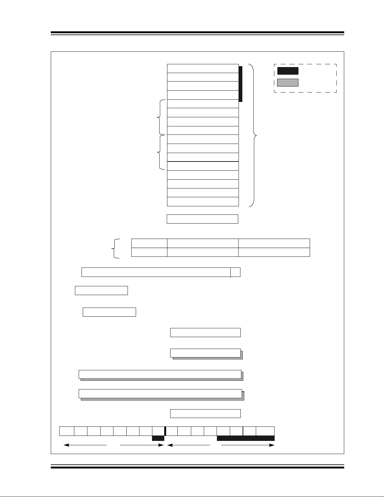
FIGURE 2-1: PROGRAMMER’S MODEL
DSP Operand
Registers
DSP Address
Registers
W0/WREG
W1
W2
W3
W4
W5
W6
W7
W8
W9
W10
W11
W12/DSP Offset
W13/DSP Write Back
W14/Frame Pointer
W15/Stack Pointer
dsPIC30F
D0D15
PUSH.S Shadow
DO Shadow
Legend
Working Registers
DSP
Accumulators
PC22
7
TABPAG
TBLPAG
7
22
22
PSVPAG
PSVPAG
AD39 AD0AD31
AccA
AccB
0
Data Table Page Address
0
SPLIM
Program Space Visibility Page Address
15
RCOUNT
15
DCOUNT
DOSTART
DOEND
PC0
Stack Pointer Limit Register
AD15
Program Counter
0
0
REPEAT Loop Counter
0
DO Loop Counter
0
DO Loop Start Address
DO Loop End Address
15
CORCON
OA OB SA SB
2004 Microchip Technology Inc. Preliminary DS70083G-page 23
OAB SAB
SRH
DA DC
IPL2 IPL1
RA
IPL0 OV
SRL
0
Core Configuration Register
N
C
Z
Status Register
Page 26

dsPIC30F
2.3 Instruction Flow
There are 8 types of instruction flows:
1. Normal one-word, one-cycle instructions: these
instructions take one effective cycle to execute
as shown in Figure 2-2.
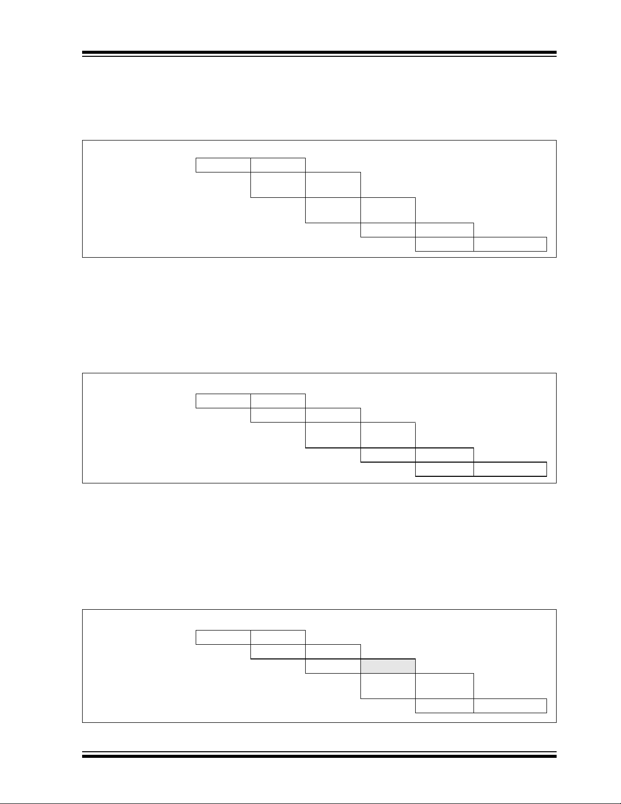
FIGURE 2-2: INSTRUCTION PIPELINE FLOW: 1-WORD, 1-CYCLE
TCY0TCY1TCY2TCY3TCY4TCY5
1. MOV.b #0x55,W0
2. MOV.b #0x35,W1
3. ADD.b W0,W1,W2
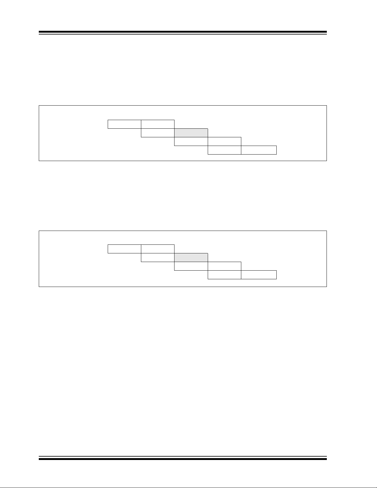
2. One-word, two-cycle (or three-cycle) instructions that are flow control instructions: these
instructions include the relative branches, relative call, skips and returns. When an instruction
changes the PC (other than to increment it), the
pipelined fetch is discarded. This causes the
instruction to take two effective cycles to execute as shown in Figure 2-3. Some instructions
that change program flow require 3 cycles, such
as the RETURN, RETFIE and RETLW instructions, and instructions that skip over 2-word
instructions.
Fetch 1 Execute 1
Fetch 2 Execute 2
Fetch 3 Execute 3
FIGURE 2-3: INSTRUCTION PIPELINE FLOW: 1-WORD, 2-CYCLE
TCY0TCY1TCY2TCY3TCY4TCY5
1. MOV #0x55,W0
2. BTSC W1,#3
3. ADD W0,W1,W2
4. BRA SUB_1
5. SUB W0,W1,W3
6. Instruction @ address SUB_1
Fetch 1 Execute 1
Fetch 2 Execute 2
Skip Taken
Fetch 3 Flush
Fetch 4 Execute 4
Fetch 5 Flush
Fetch SUB_1
DS70083G-page 24 Preliminary 2004 Microchip Technology Inc.
Page 27
dsPIC30F
3. One-word, two-cycle instructions that are not
flow control instructions: the only instructions of
this type are the MOV.D (load and store doubleword) instructions, as shown in Figure 2-4.
FIGURE 2-4: INSTRUCTION PIPELINE FLOW: 1-WORD, 2-CYCLE MOV.D OPERATIONS
TCY0TCY1TCY2TCY3TCY4TCY5
1. MOV W0,0x1234
2. MOV.D [W0++],W1
3. MOV W1,0x00AA
3a. Stall
4. MOV 0x0CC, W0
4. Table read/write instructions: these instructions
will suspend the fetching to insert a read or write
cycle to the program memory. The instruction
fetched while executing the table operation is
saved for 1 cycle and executed in the cycle
immediately after the table operation as shown
in Figure 2-5.
Fetch 1 Execute 1
Fetch 2 Execute 2
R/W Cycle 1
Fetch 3 Execute 2
R/W Cycle2
Stall Execute 3
Fetch 4 Execute 4
FIGURE 2-5: INSTRUCTION PIPELINE FLOW: 1-WORD, 2-CYCLE TABLE OPERATIONS
TCY0TCY1TCY2TCY3TCY4TCY5
1. MOV #0x1234,W0
2. TBLRDL [W0++],W1
3. MOV #0x00AA,W1
3a. Table Operation
4. MOV #0x0CC,W0
5. Two-word instructions for CALL and GOTO: in
these instructions, the fetch after the instruction
provides the remainder of the jump or call destination address. These instructions require 2
cycles to execute, 1 cycle to fetch the 2 instruction words (enabled by a high speed path on the
second fetch), and 1 cycle to flush the pipeline
as shown in Figure 2-6.
Fetch 1 Execute 1
Fetch 2 Execute 2
Fetch 3 Execute 2
Read Cycle
Bus Read Execute 3
Fetch 4 Execute 4
FIGURE 2-6: INSTRUCTION PIPELINE FLOW: 2-WORD, 2-CYCLE GOTO, CALL
TCY0TCY1TCY2TCY3TCY4TCY5
1. MOV #0x1234,W0
2. GOTO LABEL
2a. Second Word
3. Instruction @ address LABEL
4. BSET W1, #BIT3
Fetch 1 Execute 1
Fetch 2L Update PC
Fetch 2H NOP
Fetch
LABEL
Execute
LABEL
Fetch 4 Execute 4
2004 Microchip Technology Inc. Preliminary DS70083G-page 25
Page 28
dsPIC30F
6. Two-word instructions for DO: in these instructions, the fetch after the instruction contains an
address offset. This address offset is added to
the first instruction address to generate the last
loop instruction address. Therefore, these
instructions require 2 cycles as shown in
Figure 2-7.
FIGURE 2-7: INSTRUCTION PIPELINE FLOW: 2-WORD, 2-CYCLE DO, DOW
TCY0TCY1TCY2TCY3TCY4
1. PUSH DOEND
2. DO LABEL,#COUNT
2a. Second Word
3. 1st Instruction of Loop
7. Instructions that are subjected to a stall due to a
data dependency between the X RAGU and
X WAGU: an additional cycle is inserted to
resolve the resource conflict as shown in
Figure 2-7. Instruction stalls caused by data
dependencies are further discussed in
Section 4.0.
Fetch 1 Execute 1
Fetch 2L NOP
Fetch 2H Execute 2
Fetch 3 Execute 3
FIGURE 2-8: INSTRUCTION PIPELINE FLOW: 1-WORD, 2-CYCLE WITH INSTRUCTION STALL
TCY0TCY1TCY2TCY3TCY4TCY5
1. MOV.b W0,[W1]
2. MOV.b [W1],PORTB
2a. Stall (NOP)
3. MOV.b W0,PORTB
8. Interrupt recognition execution: refer to
Section 6.0 for details on interrupts.
Fetch 1 Execute 1
Fetch 2 NOP
Stall Execute 2
Fetch 3 Execute 3
DS70083G-page 26 Preliminary 2004 Microchip Technology Inc.
Page 29

dsPIC30F
2.4 Divide Support
The dsPIC devices feature a 16/16-bit signed fractional
divide operation, as well as 32/16-bit and 16/16-bit
signed and unsigned integer divide operations, in the
form of single instruction iterative divides. The following
instructions and data sizes are supported:
1. DIVF - 16/16 signed fractional divide
2. DIV.sd - 32/16 signed divide
3. DIV.ud - 32/16 unsigned divide
4. DIV.sw - 16/16 signed divide
5. DIV.uw - 16/16 unsigned divide
The 16/16 divides are similar to the 32/16 (same number
of iterations), but the dividend is either zero-extended or
sign-extended during the first iteration.
The quotient for all divide instructions is stored in W0,
and the remainder in W1. DIV and DIVF can specify
any W register for both the 16-bit dividend and divisor.
All other divides can specify any W register for the
16-bit divisor, but the 32-bit dividend must be in an
aligned W register pair, such as W1:W0, W3:W2, etc.
The non-restoring divide algorithm requires one cycle
for an initial dividend shift (for integer divides only), one
cycle per divisor bit, and a remainder/quotient correction cycle. The correction cycle is the last cycle of the
iteration loop but must be performed (even if the
remainder is not required) because it may also adjust
the quotient. A consequence of this is that DIVF will
also produce a valid remainder (though it is of little use
in fractional arithmetic).
The divide instructions must be executed within a
REPEAT loop. Any other form of execution (e.g., a
series of discrete divide instructions) will not function
correctly because the instruction flow depends on
RCOUNT. The divide instruction does not automatically
set up the RCOUNT value and it must, therefore, be
explicitly and correctly specified in the REPEAT instruction as shown in Table 2-1 (REPEAT will execute the target instruction {operand value+1} times). The REPEAT
loop count must be setup for 18 iterations of the DIV/
DIVF instruction. Thus, a complete divide operation
requires 19 cycles.
Note: The divide flow is interruptible. However,
the user needs to save the context as
appropriate.
TABLE 2-1: DIVIDE INSTRUCTIONS
Instruction Function
DIVF
DIV.sd Signed divide: (Wm+1:Wm)/Wn → W0; Rem → W1
DIV.sw or
DIV.s
DIV.ud Unsigned divide: (Wm+1:Wm)/Wn → W0; Rem → W1
DIV.uw or
DIV.u
Signed fractional divide: Wm/Wn → W0; Rem → W1
Signed divide: Wm/Wn → W0; Rem → W1
Unsigned divide: Wm/Wn → W0; Rem → W1
2004 Microchip Technology Inc. Preliminary DS70083G-page 27
Page 30

dsPIC30F
2.5 DSP Engine
Concurrent operation of the DSP engine with MCU
instruction flow is not possible, though both the MCU
ALU and DSP engine resources may be used concurrently by the same instruction (e.g., ED and EDAC
instructions).
The DSP engine consists of a high speed 17-bit x
17-bit multiplier, a barrel shifter and a 40-bit adder/
subtracter (with two target accumulators, round and
saturation logic).
Data input to the DSP engine is derived from one of the
following:
1. Directly from the W array (registers W4, W5, W6
or W7) via the X and Y data buses for the MAC
class of instructions (MAC, MSC, MPY,
MPY.N, ED, EDAC, CLR and MOVSAC).
2. From the X bus for all other DSP instructions.
3. From the X bus for all MCU instructions which
use the barrel shifter.
Data output from the DSP engine is written to one of the
following:
1. The target accumulator, as defined by the DSP
instruction being executed.
2. The X bus for MAC, MSC, CLR and MOVSAC
accumulator writes, where the EA is derived
from W13 only. (MPY, MPY.N, ED and EDAC
do not offer an accumulator write option.)
3. The X bus for all MCU instructions which use the
barrel shifter.
The DSP engine also has the capability to perform
inherent accumulator-to-accumulator operations,
which require no additional data. These instructions are
ADD, SUB and NEG.
The DSP engine has various options selected through
various bits in the CPU Core Configuration register
(CORCON), as listed below:
1. Fractional or integer DSP multiply (IF).
2. Signed or unsigned DSP multiply (US).
3. Conventional or convergent rounding (RND).
4. Automatic saturation on/off for AccA (SATA).
5. Automatic saturation on/off for AccB (SATB).
6. Automatic saturation on/off for writes to data
memory (SATDW).
7. Accumulator Saturation mode selection
(ACCSAT).
Note: For CORCON layout, see Table 4-3.
A block diagram of the DSP engine is shown in
Figure 2-9.
DS70083G-page 28 Preliminary 2004 Microchip Technology Inc.
Page 31

FIGURE 2-9: DSP ENGINE BLOCK DIAGRAM
40
Carry/Borrow Out
Carry/Borrow In
40-bit Accumulator A
40-bit Accumulator B
Saturate
Adder
Negate
40
dsPIC30F
S
a
16
Logic
t
u
r
a
t
e
Round
Y Data Bus
40
40
Sign-Extend
33
17-bit
Multiplier/Scaler
16
16
40
Barrel
Shifter
32
32
40
16
X Data Bus
16
Zero Backfill
To/From W Array
2004 Microchip Technology Inc. Preliminary DS70083G-page 29
Page 32

dsPIC30F
2.5.1 MULTIPLIER
The 17 x 17-bit multiplier is capable of signed or
unsigned operation and can multiplex its output using a
scaler to support either 1.31 fractional (Q31) or 32-bit
integer results. The respective number representation
formats are shown in Figure 2-10. Unsigned operands
are zero-extended into the 17th bit of the multiplier
input value. Signed operands are sign-extended into
the 17th bit of the multiplier input value. The output of
the 17 x 17-bit multiplier/scaler is a 33-bit value which
is sign-extended to 40 bits. Integer data is inherently
When the multiplier is configured for fractional multiplication, the data is represented as a two’s complement
fraction, where the MSB is defined as a sign bit and the
radix point is implied to lie just after the sign bit (QX
format). The range of an N-bit two’s complement fraction with this implied radix point is -1.0 to (1 – 2
a 16-bit fraction, the Q15 data range is -1.0 (0x8000)
to 0.999969482 (0x7FFF) including ‘0’ and has a
precision of 3.01518x10
16x16 multiply operation generates a 1.31 product
which has a precision of 4.65661 x 10
represented as a signed two’s complement value,
where the MSB is defined as a sign bit. Generally
speaking, the range of an N-bit two’s complement integer is -2
N-1
to 2
N-1
– 1. For a 16-bit integer, the data
range is -32768 (0x8000) to 32767 (0x7FFF) including
‘0’ (see Figure 2-10). For a 32-bit integer, the data
range is -2,147,483,648 (0x8000 0000) to
2,147,483,645 (0x7FFF FFFF).
FIGURE 2-10: 16-BIT INTEGER AND FRACTIONAL MODES
Different Representations of 0x4001
Integer:
0 1 0 0 0 0 0 0 0 0 0 0 0 0 0 1
14
0
2
0x4001 = 2
13 212 211
2
14
+ 20 = 16385
.... 2
1-N
). For
-5
. In Fractional mode, the
-10
.
0
2
1.15 Fractional:
0 1 0 0 0 0 0 0 0 0 0 0 0 0 0 1
0
-1
-2
. 2
0x4001 = 2-1 + 2
2
-2 2-3
-15
. . .
= 0.500030518
Certain multiply operations always operate on signed
data. These include the MAC/MSC, MPY[.N] and
ED[AC] instructions. The 40-bit adder/subtracter may
also optionally negate one of its operand inputs to
change the result sign (without changing the operands). This is used to create a multiply and subtract
(MSC), or multiply and negate (MPY.N) operation.
In the special case when both input operands are 1.15
fractions and equal to 0x8000 (-1
), the result of the
10
multiplication is corrected to 0x7FFFFFFF (as the
closest approximation to +1) by hardware before it is
used.
It should be noted that with the exception of DSP multiplies, the dsPIC30F ALU operates identically on integer and fractional data. Namely, an addition of two
integers will yield the same result (binary number) as
the addition of two fractional numbers. The only difference is how the result is interpreted by the user. However, multiplies performed by DSP operations are
-15
2
different. In these instructions, data format selection is
made with the IF bit (CORCON<0>) and US bits
(CORCON<12>), and it must be set accordingly (‘0’ for
Fractional mode, ‘1’ for Integer mode in the case of the
IF bit, and ‘0’ for Signed mode, ‘1’ for Unsigned mode
in the case of the US bit). This is required because of
the implied radix point used by dsPIC30F fractions. In
Integer mode, multiplying two 16-bit integers produces
a 32-bit integer result. However, multiplying two 1.15
values generates a 2.30 result. Since the dsPIC30F
uses 1.31 format for the accumulators, a DSP multiply
in Fractional mode also includes a left shift by one bit to
keep the radix point properly aligned. This feature
reduces the resolution of the DSP multiplier to 2
-30
, but
has no other effect on the computation.
DS70083G-page 30 Preliminary 2004 Microchip Technology Inc.
Page 33

dsPIC30F
The same multiplier is used to support the MCU multiply instructions which include integer 16-bit signed,
unsigned and mixed sign multiplies. Additional data
paths are provided to allow these instructions to write
the result back into the W array and X data bus (via the
W array). These paths are placed prior to the data
scaler. The IF bit in the CORCON register, therefore,
only affects the result of the MAC class of DSP instructions. All other multiply operations are assumed to be
integer operations. If the user executes a MAC instruction on fractional data without clearing the IF bit, the
result must be explicitly shifted left by the user program
after multiplication in order to obtain the correct result.
The MUL instruction may be directed to use byte or
word sized operands. Byte operands will direct a 16-bit
result, and word operands will direct a 32-bit result to
the specified register(s) in the W array.
2.5.2 DATA ACCUMULATORS AND
ADDER/SUBTRACTER
The data accumulator consists of a 40-bit adder/
subtracter with automatic sign extension logic. It can
select one of two accumulators (A or B) as its preaccumulation source and post-accumulation destination. For the ADD and LAC instructions, the data to be
accumulated or loaded can be optionally scaled via the
barrel shifter, prior to accumulation.
2.5.2.1 Adder/Subtracter, Overflow and
Saturation
The adder/subtracter is a 40-bit adder with an optional
zero input into one side and either true, or complement
data into the other input. In the case of addition, the
carry/borrow
true data (not complemented), whereas in the case of
subtraction, the carry/borrow
other input is complemented. The adder/subtracter
generates overflow status bits SA/SB and OA/OB,
which are latched and reflected in the STATUS register:
• Overflow from bit 39: this is a catastrophic
overflow in which the sign of the accumulator is
destroyed.
• Overflow into guard bits 32 through 39: this is a
recoverable overflow. This bit is set whenever all
the guard bits bits are not identical to each other.
The adder has an additional saturation block which
controls accumulator data saturation, if selected. It
uses the result of the adder, the overflow status bits
described above, and the SATA/B (CORCON<7:6>)
and ACCSAT (CORCON<4>) mode control bits to
determine when and to what value to saturate.
input is active high and the other input is
input is active low and the
Six STATUS register bits have been provided to
support saturation and overflow; they are:
1. OA:
AccA overflowed into guard bits
2. OB:
AccB overflowed into guard bits
3. SA:
AccA saturated (bit 31 overflow and saturation)
or
AccA overflowed into guard bits and saturated
(bit 39 overflow and saturation)
4. SB:
AccB saturated (bit 31 overflow and saturation)
or
AccB overflowed into guard bits and saturated
(bit 39 overflow and saturation)
5. OAB:
Logical OR of OA and OB
6. SAB:
Logical OR of SA and SB
The OA and OB bits are modified each time data
passes through the adder/subtracter. When set, they
indicate that the most recent operation has overflowed
into the accumulator guard bits (bits 32 through 39).
The OA and OB bits can also optionally generate an
arithmetic warning trap when set and the corresponding overflow trap flag enable bit (OVATEN, OVBTEN) in
the INTCON1 register (refer to Section 5.0) is set. This
allows the user to take immediate action, for example,
to correct system gain.
The SA and SB bits are modified each time data
passes through the adder/subtracter but can only be
cleared by the user. When set, they indicate that the
accumulator has overflowed its maximum range (bit 31
for 32-bit saturation, or bit 39 for 40-bit saturation) and
will be saturated (if saturation is enabled). When saturation is not enabled, SA and SB default to bit 39 overflow and thus indicate that a catastrophic overflow has
occurred. If the COVTE bit in the INTCON1 register is
set, SA and SB bits will generate an arithmetic warning
trap when saturation is disabled.
The overflow and saturation status bits can optionally
be viewed in the STATUS register (SR) as the logical
OR of OA and OB (in bit OAB) and the logical OR of SA
and SB (in bit SAB). This allows programmers to check
one bit in the STATUS register to determine if either
accumulator has overflowed, or one bit to determine if
either accumulator has saturated. This would be useful
for complex number arithmetic which typically uses
both the accumulators.
2004 Microchip Technology Inc. Preliminary DS70083G-page 31
Page 34

dsPIC30F
The device supports three saturation and overflow
modes:
1. Bit 39 Overflow and Saturation:
When bit 39 overflow and saturation occurs, the
saturation logic loads the maximally positive 9.31
(0x7FFFFFFFFF), or maximally negative 9.31
value (0x8000000000) into the target accumulator. The SA or SB bit is set and remains set until
cleared by the user. This is referred to as ‘super
saturation’ and provides protection against erroneous data, or unexpected algorithm problems
(e.g., gain calculations).
2. Bit 31 Overflow and Saturation:
When bit 31 overflow and saturation occurs, the
saturation logic then loads the maximally positive 1.31 value (0x007FFFFFFF), or maximally
negative 1.31 value (0x0080000000) into the
target accumulator. The SA or SB bit is set and
remains set until cleared by the user. When this
Saturation mode is in effect, the guard bits are
not used (so the OA, OB or OAB bits are never
set).
3. Bit 39 Catastrophic Overflow:
The bit 39 overflow status bit from the adder is
used to set the SA or SB bit which remain set
until cleared by the user. No saturation operation
is performed and the accumulator is allowed to
overflow (destroying its sign). If the COVTE bit in
the INTCON1 register is set, a catastrophic
overflow can initiate a trap exception.
2.5.2.2 Accumulator ‘Write Back’
The MAC class of instructions (with the exception of
MPY, MPY.N, ED and EDAC) can optionally write a
rounded version of the high word (bits 31 through 16)
of the accumulator that is not targeted by the instruction
into data space memory. The write is performed across
the X bus into combined X and Y address space. The
following Addressing modes are supported:
1. W13, Register Direct:
The rounded contents of the non-target
accumulator are written into W13 as a 1.15
fraction.
2. [W13]+=2, Register Indirect with Post-Increment:
The rounded contents of the non-target accumulator are written into the address pointed to by
W13 as a 1.15 fraction. W13 is then
incremented by 2 (for a word write).
2.5.2.3 Round Logic
The round logic is a combinational block which performs a conventional (biased) or convergent (unbiased) round function during an accumulator write
(store). The Round mode is determined by the state of
the RND bit in the CORCON register. It generates a 16bit, 1.15 data value which is passed to the data space
write saturation logic. If rounding is not indicated by the
instruction, a truncated 1.15 data value is stored and
the LS Word is simply discarded.
The two Rounding modes are shown in Figure 2-10.
Conventional rounding takes bit 15 of the accumulator,
zero-extends it and adds it to the ACCxH word (bits 16
through 31 of the accumulator). If the ACCxL word
(bits 0 through 15 of the accumulator) is between
0x8000 and 0xFFFF (0x8000 included), ACCxH is
incremented. If ACCxL is between 0x0000 and
0x7FFF, ACCxH is left unchanged. A consequence of
this algorithm is that over a succession of random
rounding operations, the value will tend to be biased
slightly positive.
Convergent (or unbiased) rounding operates in the
same manner as conventional rounding, except when
ACCxL equals 0x8000. If this is the case, the LS bit
(bit 16 of the accumulator) of ACCxH is examined. If it
is ‘1’, ACCxH is incremented. If it is ‘0’, ACCxH is not
modified. Assuming that bit 16 is effectively random in
nature, this scheme will remove any rounding bias that
may accumulate.
The SAC and SAC.R instructions store either a truncated (SAC) or rounded (SAC.R) version of the contents
of the target accumulator to data memory via the X bus
(subject to data saturation, see Section 2.5.2.4). Note
that for the MAC class of instructions, the accumulator
write back operation will function in the same manner,
addressing combined MCU (X and Y) data space
though the X bus. For this class of instructions, the data
is always subject to rounding.
DS70083G-page 32 Preliminary 2004 Microchip Technology Inc.
Page 35

dsPIC30F
2.5.2.4 Data Space Write Saturation
In addition to adder/subtracter saturation, writes to data
space may also be saturated but without affecting the
contents of the source accumulator. The data space
write saturation logic block accepts a 16-bit, 1.15 fractional value from the round logic block as its input,
together with overflow status from the original source
(accumulator) and the 16-bit round adder. These are
combined and used to select the appropriate 1.15
fractional value as output to write to data space
memory.
If the SATDW bit in the CORCON register is set, data
(after rounding or truncation) is tested for overflow and
adjusted accordingly, For input data greater than
0x007FFF, data written to memory is forced to the
maximum positive 1.15 value, 0x7FFF. For input data
less than 0xFF8000, data written to memory is forced
to the maximum negative 1.15 value, 0x8000. The MS
bit of the source (bit 39) is used to determine the sign
of the operand being tested.
If the SATDW bit in the CORCON register is not set, the
input data is always passed through unmodified under
all conditions.
2.5.3 BARREL SHIFTER
The barrel shifter is capable of performing up to 15-bit
arithmetic or logic right shifts, or up to 16-bit left shifts
in a single cycle. The source can be either of the two
DSP accumulators, or the X bus (to support multi-bit
shifts of register or memory data).
The shifter requires a signed binary value to determine
both the magnitude (number of bits) and direction of the
shift operation. A positive value will shift the operand
right. A negative value will shift the operand left. A
value of ‘0’ will not modify the operand.
The barrel shifter is 40-bits wide, thereby obtaining a
40-bit result for DSP shift operations and a 16-bit result
for MCU shift operations. Data from the X bus is presented to the barrel shifter between bit positions 16 to
31 for right shifts, and bit positions 0 to 15 for left shifts.
2004 Microchip Technology Inc. Preliminary DS70083G-page 33
Page 36

dsPIC30F
NOTES:
DS70083G-page 34 Preliminary 2004 Microchip Technology Inc.
Page 37
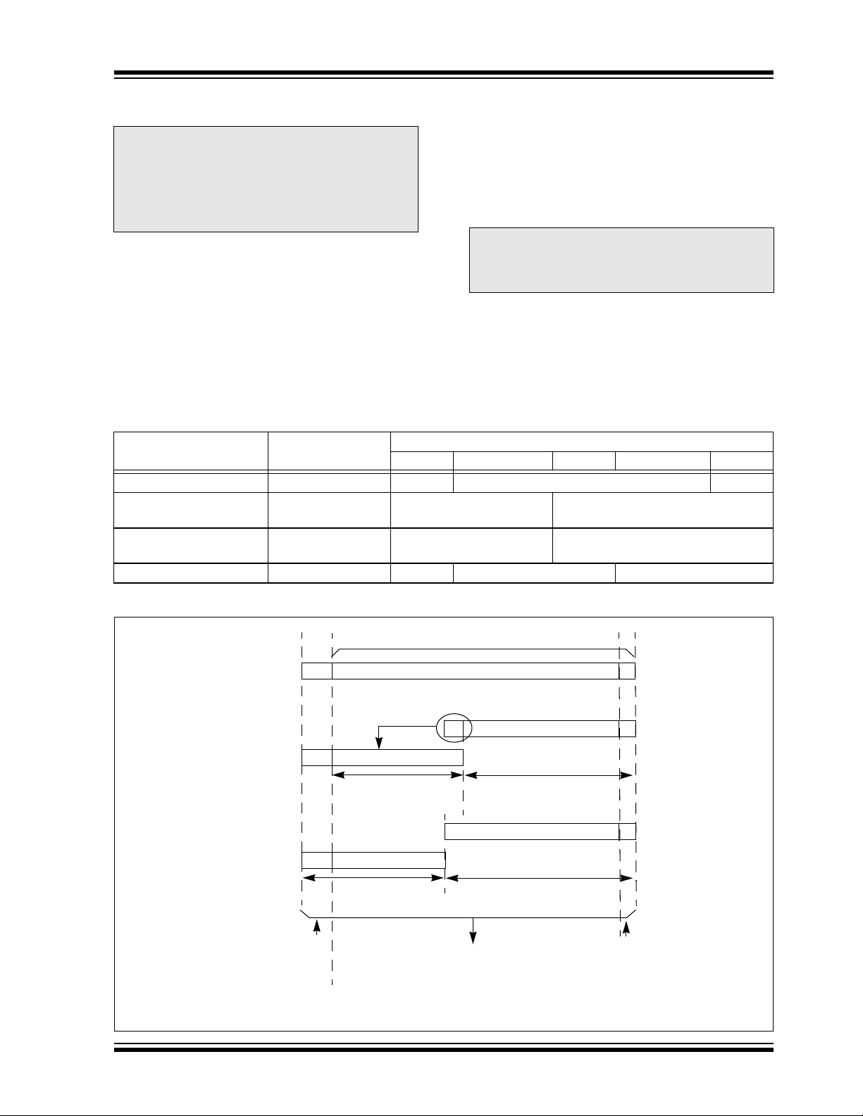
dsPIC30F
3.0 MEMORY ORGANIZATION
User program space access is restricted to the lower
4M instruction word address range (0x000000 to
Note: This data sheet summarizes features of this group
of dsPIC30F devices and is not intended to be a complete
reference source. For more information on the CPU,
peripherals, register descriptions and general device
functionality, refer to the dsPIC30F Family Reference
Manual (DS70046). For more information on the device
instruction set and programming, refer to the dsPIC30F
Programmer’s Reference Manual (DS70030).
0x7FFFFE) for all accesses other than TBLRD/TBLWT,
which use TBLPAG<7> to determine user or configuration space access. In Table 3-1, Program Space
Address Construction, bit 23 allows access to the
Device ID, the User ID and the configuration bits.
Otherwise, bit 23 is always clear.
Note: The address map shown in Figure 3-5 is
3.1 Program Address Space
The program address space is 4M instruction words. It
conceptual, and the actual memory configuration may vary across individual
devices depending on available memory.
is addressable by a 24-bit value from either the 23-bit
PC, table instruction EA, or data space EA, when pro-
gram space is mapped into data space as defined by
Table 3-1. Note that the program space address is
incremented by two between successive program
words in order to provide compatibility with data space
addressing.
TABLE 3-1: PROGRAM SPACE ADDRESS CONSTRUCTION
Access Type
Access
Space
<23> <22:16> <15> <14:1> <0>
Instruction Access User 0 PC<22:1> 0
TBLRD/TBLWT User
TBLPAG<7:0> Data EA<15:0>
(TBLPAG<7> = 0)
TBLRD/TBLWT Configuration
TBLPAG<7:0> Data EA<15:0>
(TBLPAG<7> = 1)
Program Space Visibility User 0 PSVPAG<7:0> Data EA<14:0>
Program Space Address
FIGURE 3-1: DATA ACCESS FROM PROGRAM SPACE ADDRESS GENERATION
23 bits
Using
Program
Counter
Using
Program
Space
Visibility
Using
Table
Instruction
User/
Configuration
Space
Select
0
0
PSVPAG Reg
1/0
TBLPAG Reg
8 bits
8 bits
Select
1
24-bit EA
EA
15 bits
EA
16 bits
Note: Program space visibility cannot be used to access bits <23:16> of a word in program memory.
0Program Counter
Byte
Select
2004 Microchip Technology Inc. Preliminary DS70083G-page 35
Page 38
dsPIC30F
3.1.1 PROGRAM SPACE ALIGNMENT
AND DATA ACCESS USING TABLE
INSTRUCTIONS
This architecture fetches 24-bit wide program memory.
Consequently, instructions are always aligned.
However, as the architecture is modified Harvard, data
can also be present in program space.
There are two methods by which program space can
be accessed: via special table instructions, or through
the remapping of a 16K word program space page into
the upper half of data space (see Section 3.1.2). The
TBLRDL and TBLWTL instructions offer a direct method
of reading or writing the LS Word of any address within
program space, without going through data space. The
TBLRDH and TBLWTH instructions are the only method
whereby the upper 8 bits of a program space word can
be accessed as data.
The PC is incremented by two for each successive
24-bit program word. This allows program memory
addresses to directly map to data space addresses.
Program memory can thus be regarded as two 16-bit
word wide address spaces, residing side by side, each
with the same address range. TBLRDL and TBLWTL
access the space which contains the LS Data Word,
and TBLRDH and TBLWTH access the space which
contains the MS Data Byte.
Figure 3-1 shows how the EA is created for table operations and data space accesses (PSV = 1). Here,
P<23:0> refers to a program space word, whereas
D<15:0> refers to a data space word.
A set of table instructions are provided to move byte or
word sized data to and from program space.
1. TBLRDL: Table Read Low
Word: Read the LS Word of the program address;
P<15:0> maps to D<15:0>.
Byte: Read one of the LS Bytes of the program
address;
P<7:0> maps to the destination byte when byte
select = 0;
P<15:8> maps to the destination byte when byte
select = 1.
2. TBLWTL: Table Write Low (refer to Section 6.0
for details on Flash Programming)
3. TBLRDH: Table Read High
Word: Read the MS Word of the program address;
P<23:16> maps to D<7:0>; D<15:8> will always
be = 0.
Byte: Read one of the MS Bytes of the program
address;
P<23:16> maps to the destination byte when
byte select = 0;
The destination byte will always be = 0 when
byte select = 1.
4. TBLWTH: Table Write High (refer to Section 6.0
for details on Flash Programming)
FIGURE 3-2: PROGRAM DATA TABLE ACCESS (LS WORD)
PC Address
0x000000
0x000002
0x000004
0x000006
Program Memory
‘Phantom’ Byte
(read as ‘0’)
00000000
00000000
00000000
00000000
23
TBLRDL.W
16
TBLRDL.B (Wn<0> = 1)
8
TBLRDL.B (Wn<0> = 0)
0
DS70083G-page 36 Preliminary 2004 Microchip Technology Inc.
Page 39

FIGURE 3-3: PROGRAM DATA TABLE ACCESS (MS BYTE)
TBLRDH.W
dsPIC30F
PC Address
0x000000
0x000002
0x000004
0x000006
Program Memory
‘Phantom’ Byte
(read as ‘0’)
00000000
00000000
00000000
00000000
23
TBLRDH.B (Wn<0> = 1)
3.1.2 PROGRAM SPACE VISIBILITY
FROM DATA SPACE
The upper 32 Kbytes of data space may optionally be
mapped into any 16K word program space page. This
provides transparent access of stored constant data
from X data space without the need to use special
instructions (i.e., TBLRDL/H, TBLWTL/H instructions).
Program space access through the data space occurs
if the MS bit of the data space EA is set and program
space visibility is enabled by setting the PSV bit in the
Core Control register (CORCON). The functions of
CORCON are discussed in Section 2.5, DSP Engine.
Data accesses to this area add an additional cycle to
the instruction being executed, since two program
memory fetches are required.
Note that the upper half of addressable data space is
always part of the X data space. Therefore, when a
DSP operation uses program space mapping to access
this memory region, Y data space should typically contain state (variable) data for DSP operations, whereas
X data space should typically contain coefficient
(constant) data.
Although each data space address, 0x8000 and
higher, maps directly into a corresponding program
memory address (see Figure 3-4), only the lower
16 bits of the 24-bit program word are used to contain
the data. The upper 8 bits should be programmed to
force an illegal instruction to maintain machine robustness. Refer to the Programmer’s Reference Manual
(DS70030) for details on instruction encoding.
16
TBLRDH.B (Wn<0> = 0)
Note that by incrementing the PC by 2 for each
program memory word, the LS 15 bits of data space
addresses directly map to the LS 15 bits in the corresponding program space addresses. The remaining
bits are provided by the Program Space Visibility Page
register, PSVPAG<7:0>, as shown in Figure 3-4.
Note: PSV access is temporarily disabled during
table reads/writes.
For instructions that use PSV which are executed
outside a REPEAT loop:
• The following instructions will require one
instruction cycle in addition to the specified
execution time:
- MAC class of instructions with data operand
pre-fetch
- MOV instructions
- MOV.D instructions
• All other instructions will require two instruction
cycles in addition to the specified execution time
of the instruction.
For instructions that use PSV which are executed
inside a REPEAT loop:
• The following instances will require two instruction
cycles in addition to the specified execution time
of the instruction:
- Execution in the first iteration
- Execution in the last iteration
- Execution prior to exiting the loop due to an
interrupt
- Execution upon re-entering the loop after an
interrupt is serviced
• Any other iteration of the REPEAT loop will allow
the instruction accessing data, using PSV, to
execute in a single cycle.
8
0
2004 Microchip Technology Inc. Preliminary DS70083G-page 37
Page 40
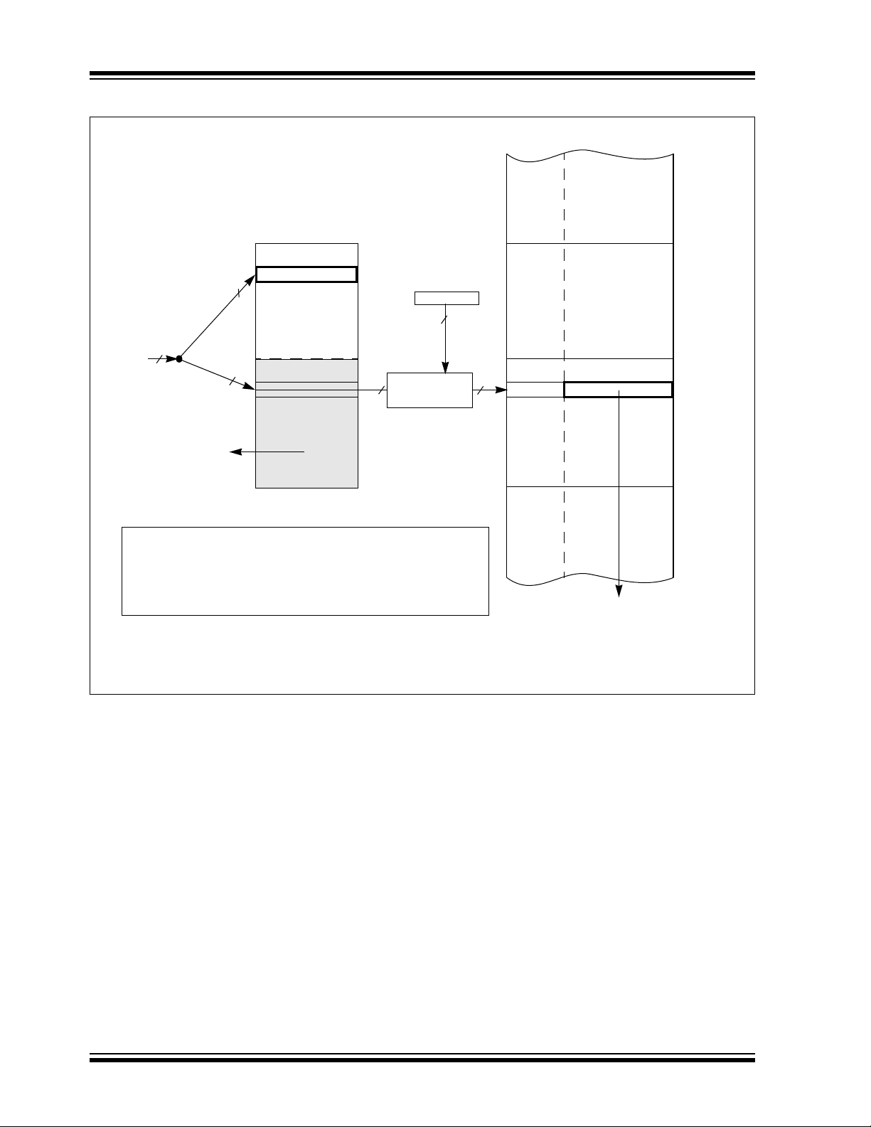
dsPIC30F
FIGURE 3-4: DATA SPACE WINDOW INTO PROGRAM SPACE OPERATION
Program Space
Data Space
0x0000
0x21
(1)
8
23 15 0
23
Data Read
0x108000
0x108200
0x10FFFF
EA<15> =
16
Data
Space
EA
EA<15> = 1
Upper Half of Data
Space is Mapped
into Program Space
BSET CORCON,#2 ; PSV bit set
MOV #0x21, W0 ; Set PSVPAG register
MOV W0, PSVPAG
MOV 0x8200, W0 ; Access program memory location
Note: PSVPAG is an 8-bit register, containing bits <22:15> of the program space address (i.e., it defines
the page in program space to which the upper half of data space is being mapped).
15
0
15
; using a data space access
0x8000
15
0xFFFF
PSVPAG
Address
Concatenation
DS70083G-page 38 Preliminary 2004 Microchip Technology Inc.
Page 41

dsPIC30F
FIGURE 3-5: SAMPLE PROGRAM
SPACE MEMORY MAP
Reset - GOTO Instruction
Reset - Target Address
Interrupt Vector Table
Alternate Vector Table
Space
User Memory
Space
Configuration Memory
Program Memory
(48K instructions)
UNITID (32 instr.)
Device Configuration
Reserved
User Flash
Reserved
(Read ‘0’s)
Data EEPROM
(4 Kbytes)
Reserved
Reserved
Registers
Reserved
000000
000002
000004
Vector Tables
00007E
000080
000084
0000FE
000100
017FFE
018000
7FEFFE
7FF000
7FFFFE
800000
8005BE
8005C0
8005FE
800600
F7FFFE
F80000
F8000E
F80010
3.2 Data Address Space
The core has two data spaces. The data spaces can be
considered either separate (for some DSP instructions), or as one unified linear address range (for MCU
instructions). The data spaces are accessed using two
Address Generation Units (AGUs) and separate data
paths.
3.2.1 DATA SPACES
The X data space is used by all instructions and supports all Addressing modes. There are separate read
and write data buses. The X read data bus is the return
data path for all instructions that view data space as
combined X and Y address space. It is also the X
address space data path for the dual operand read
instructions (MAC class). The X write data bus is the
only write path to data space for all instructions.
The X data space also supports modulo addressing for
all instructions, subject to Addressing mode restrictions. Bit-reversed addressing is only supported for
writes to X data space.
The Y data space is used in concert with the X data
space by the MAC class of instructions (CLR, ED,
EDAC, MAC, MOVSAC, MPY, MPY.N and MSC) to
provide two concurrent data read paths. No writes
occur across the Y bus. This class of instructions dedicates two W register pointers, W10 and W11, to always
address Y data space, independent of X data space,
whereas W8 and W9 always address X data space.
Note that during accumulator write back, the data
address space is considered a combination of X and Y
data spaces, so the write occurs across the X bus.
Consequently, the write can be to any address in the
entire data space.
The Y data space can only be used for the data prefetch operation associated with the MAC class of
instructions. It also supports modulo addressing for
automated circular buffers. Of course, all other instructions can access the Y data address space through the
X data path as part of the composite linear space.
The boundary between the X and Y data spaces is
defined as shown in Figure 3-8 and is not user programmable. Should an EA point to data outside its own
assigned address space, or to a location outside physical memory, an all zero word/byte will be returned. For
example, although Y address space is visible by all
non-MAC instructions using any Addressing mode, an
attempt by a MAC instruction to fetch data from that
space using W8 or W9 (X space pointers) will return
0x0000.
FEFFFE
DEVID (2)
Note: These address boundaries may vary from one
device to another.
2004 Microchip Technology Inc. Preliminary DS70083G-page 39
FF0000
FFFFFE
Page 42

dsPIC30F
TABLE 3-2: EFFECT OF INVALID
MEMORY ACCESSES
Attempted Operation Data Returned
EA = an unimplemented address 0x0000
W8 or W9 used to access Y data
space in a MAC instruction
W10 or W11 used to access X
data space in a MAC instruction
All effective addresses are 16 bits wide and point to
bytes within the data space. Therefore, the data space
address range is 64 Kbytes or 32K words.
0x0000
0x0000
3.2.2 DATA SPACE WIDTH
The core data width is 16 bits. All internal registers are
organized as 16-bit wide words. Data space memory is
organized in byte addressable, 16-bit wide blocks.
3.2.3 DATA ALIGNMENT
To help maintain backward compatibility with
PICmicro
usage efficiency, the dsPIC30F instruction set supports
both word and byte operations. Data is aligned in data
memory and registers as words, but all data space EAs
resolve to bytes. Data byte reads will read the complete
word which contains the byte, using the LS bit of any
EA to determine which byte to select. The selected byte
is placed onto the LS Byte of the X data path (no byte
accesses are possible from the Y data path as the MAC
class of instruction can only fetch words). That is, data
memory and registers are organized as two parallel
byte wide entities with shared (word) address decode
but separate write lines. Data byte writes only write to
the corresponding side of the array or register which
matches the byte address.
As a consequence of this byte accessibility, all effective
address calculations (including those generated by the
DSP operations which are restricted to word sized
data) are internally scaled to step through word aligned
memory. For example, the core would recognize that
Post-Modified Register Indirect Addressing mode
[Ws++] will result in a value of Ws+1 for byte operations
and Ws+2 for word operations.
All word accesses must be aligned to an even address.
Misaligned word data fetches are not supported so
care must be taken when mixing byte and word operations, or translating from 8-bit MCU code. Should a misaligned read or write be attempted, an address error
trap will be generated. If the error occurred on a read,
the instruction underway is completed, whereas if it
occurred on a write, the instruction will be executed but
the write will not occur. In either case, a trap will then
be executed, allowing the system and/or user to examine the machine state prior to execution of the address
fault.
®
devices and improve data space memory
FIGURE 3-6: DATA ALIGNMENT
15 8 7 0
0001
0003
0005
All byte loads into any W register are loaded into the LS
Byte. The MSB is not modified.
A sign-extend (SE) instruction is provided to allow
users to translate 8-bit signed data to 16-bit signed
values. Alternatively, for 16-bit unsigned data, users
can clear the MSB of any W register by executing a
zero-extend (ZE) instruction on the appropriate
address.
Although most instructions are capable of operating on
word or byte data sizes, it should be noted that some
instructions, including the DSP instructions, operate
only on words.
Byte1 Byte 0
Byte3 Byte 2
Byte5 Byte 4
LS ByteMS Byte
0000
0002
0004
3.2.4 DATA SPACE MEMORY MAP
The data space memory is split into two blocks, X and
Y data space. A key element of this architecture is that
Y space is a subset of X space, and is fully contained
within X space. In order to provide an apparent linear
addressing space, X and Y spaces have contiguous
addresses.
When executing any instruction other than one of the
MAC class of instructions, the X block consists of the 64Kbyte data address space (including all Y addresses).
When executing one of the MAC class of instructions,
the X block consists of the 64-Kbyte data address
space excluding the Y address block (for data reads
only). In other words, all other instructions regard the
entire data memory as one composite address space.
The MAC class instructions extract the Y address space
from data space and address it using EAs sourced from
W10 and W11. The remaining X data space is
addressed using W8 and W9. Both address spaces are
concurrently accessed only with the MAC class
instructions.
An example data space memory map is shown in
Figure 3-8.
DS70083G-page 40 Preliminary 2004 Microchip Technology Inc.
Page 43

dsPIC30F
3.2.5 NEAR DATA SPACE
An 8-Kbyte ‘near’ data space is reserved in X address
memory space between 0x0000 and 0x1FFF, which is
directly addressable via a 13-bit absolute address field
within all memory direct instructions. The remaining X
address space and all of the Y address space is
addressable indirectly. Additionally, the whole of X data
space is addressable using MOV instructions, which
support memory direct addressing with a 16-bit
address field.
The stack pointer always points to the first available
free word and grows from lower addresses towards
higher addresses. It pre-decrements for stack pops and
post-increments for stack pushes as shown in Figure 3-
7. Note that for a PC push during any CALL instruction,
the MSB of the PC is zero-extended before the push,
ensuring that the MSB is always clear.
Note: A PC push during exception processing
will concatenate the SRL register to the
MSB of the PC prior to the push.
3.2.6 SOFTWARE STACK
The dsPIC devices contain a software stack. W15 is
used as the stack pointer.
There is a Stack Pointer Limit register (SPLIM) associated with the stack pointer. SPLIM is uninitialized at
Reset. As is the case for the stack pointer, SPLIM<0>
is forced to ‘0’ because all stack operations must be
word aligned. Whenever an effective address (EA) is
generated using W15 as a source or destination
pointer, the address thus generated is compared with
the value in SPLIM. If the contents of the Stack Pointer
(W15) and the SPLIM register are equal and a push
operation is performed, a Stack Error Trap will not
occur. The Stack Error Trap will occur on a subsequent
push operation. Thus, for example, if it is desirable to
cause a Stack Error Trap when the stack grows beyond
address 0x2000 in RAM, initialize the SPLIM with the
value, 0x1FFE.
Similarly, a stack pointer underflow (stack error) trap is
generated when the stack pointer address is found to
be less than 0x0800, thus preventing the stack from
interfering with the Special Function Register (SFR)
space.
A write to the SPLIM register should not be immediately
followed by an indirect read operation using W15.
FIGURE 3-7: CALL STACK FRAME
0x0000
Higher Address
Stack Grows Towards
PC<15:0>
000000000
<Free Word>
PC<22:16>
015
W15 (before CALL)
W15 (after CALL)
POP : [--W15]
PUSH : [W15++]
2004 Microchip Technology Inc. Preliminary DS70083G-page 41
Page 44

dsPIC30F
FIGURE 3-8: SAMPLE DATA SPACE MEMORY MAP
2-Kbyte
SFR Space
8-Kbyte
SRAM Space
MS Byte
Address
0x0001
0x07FF
0x0801
0x17FF
0x1801
0x27FF 0x27FE
0x8001
16 bits
LSBMSB
SFR Space
X Data RAM (X)
Y Data RAM (Y)
LS Byte
Address
0x0000
0x07FE
0x0800
0x17FE
0x1800
0x1FFE 0x1FFF
0x28000x2801
0x8000
8-Kbyte
Near
Data
Space
X Data
Unimplemented (X)
Optionally
Mapped
into Program
Memory
0xFFFF
Note: The address map shown in Figure 3-8 is conceptual, and may vary across individual devices
depending on available memory.
0xFFFE
DS70083G-page 42 Preliminary 2004 Microchip Technology Inc.
Page 45

dsPIC30F
FIGURE 3-9: DATA SPACE FOR MCU AND DSP (MAC CLASS) INSTRUCTIONS EXAMPLE
SFR SPACE
UNUSED
(Y SPACE)
X SPACE
Non-MAC Class Ops (Read/Write)
MAC Class Ops (Write)
Indirect EA from any W Indirect EA from W8, W9 Indirect EA from W10, W11
Y SPACE
UNUSED
MAC Class Ops (Read)
SFR SPACE
UNUSED
X SPACE
X SPACE
2004 Microchip Technology Inc. Preliminary DS70083G-page 43
Page 46

dsPIC30F
uuuu uuuu uuuu uuu0
0
Bit 15 Bit 14 Bit 13 Bit 12 Bit 11 Bit 10 Bit 9 Bit 8 Bit 7 Bit 6 Bit 5 Bit 4 Bit 3 Bit 2 Bit 1 Bit 0 Reset State
(Home)
Address
SFR Name
TABLE 3-3: CORE REGISTER MAP
W2 0004 W2 0000 0000 0000 0000
W0 0000 W0 / WREG 0000 0000 0000 0000
W1 0002 W1 0000 0000 0000 0000
W5 000A W5 0000 0000 0000 0000
W4 0008 W4 0000 0000 0000 0000
W3 0006 W3 0000 0000 0000 0000
W10 0014 W10 0000 0000 0000 0000
W11 0016 W11 0000 0000 0000 0000
W9 0012 W9 0000 0000 0000 0000
W8 0010 W8 0000 0000 0000 0000
W7 000E W7 0000 0000 0000 0000
W6 000C W6 0000 0000 0000 0000
W12 0018 W12 0000 0000 0000 0000
W13 001A W13 0000 0000 0000 0000
W14 001C W14 0000 0000 0000 0000
ACCAL 0022 ACCAL 0000 0000 0000 0000
W15 001E W15 0000 1000 0000 0000
SPLIM 0020 SPLIM 0000 0000 0000 0000
ACCBU 002C Sign-Extension (ACCB<39>) ACCBU 0000 0000 0000 0000
PCL 002E PCL 0000 0000 0000 0000
ACCBH 002A ACCBH 0000 0000 0000 0000
ACCAU 0026 Sign-Extension (ACCA<39>) ACCAU 0000 0000 0000 0000
ACCBL 0028 ACCBL 0000 0000 0000 0000
ACCAH 0024 ACCAH 0000 0000 0000 0000
— — — — — — — — PSVPAG 0000 0000 0000 0000
PCH 0030
PSVPAG 0034
RCOUNT 0036 RCOUNT uuuu uuuu uuuu uuuu
TBLPAG 0032
— — — — — — — — — DOSTARTH 0000 0000 0uuu uuuu
— — — — — — — — — DOENDH 0000 0000 0uuu uuuu
DOSTARTL 003A DOSTARTL 0 uuuu uuuu uuuu uuu0
DOSTARTH 003C
DCOUNT 0038 DCOUNT uuuu uuuu uuuu uuuu
DOENDL 003E DOENDL
DOENDH 0040
SR 0042 OA OB SA SB OAB SAB DA DC IPL2 IPL1 IPL0 RA N OV Z C 0000 0000 0000 0000
Legend: u = uninitialized bit
— — — — — — — — — PCH 0000 0000 0000 0000
— — — — — — — —TBLPAG0000 0000 0000 0000
DS70083G-page 44 Preliminary 2004 Microchip Technology Inc.
Page 47

dsPIC30F
— — BWM<3:0> YWM<3:0> XWM<3:0> 0000 0000 0000 0000
Bit 15 Bit 14 Bit 13 Bit 12 Bit 11 Bit 10 Bit 9 Bit 8 Bit 7 Bit 6 Bit 5 Bit 4 Bit 3 Bit 2 Bit 1 Bit 0 Reset State
(Home)
Address
SFR Name
CORCON 0044 — — — US EDT DL2 DL1 DL0 SATA SATB SATDW ACCSAT IPL3 PSV RND IF 0000 0000 0010 0000
MODCON 0046 XMODEN YMODEN
XMODSRT 0048 XS<15:1> 0 uuuu uuuu uuuu uuu0
XMODEND 004A XE<15:1> 1 uuuu uuuu uuuu uuu1
TABLE 3-3: CORE REGISTER MAP (CONTINUED)
2004 Microchip Technology Inc. Preliminary DS70083G-page 45
YMODSRT 004C YS<15:1> 0 uuuu uuuu uuuu uuu0
— — DISICNT<13:0> 0000 0000 0000 0000
YMODEND 004E YE<15:1> 1 uuuu uuuu uuuu uuu1
Legend: u = uninitialized bit
XBREV 0050 BREN XB<14:0> uuuu uuuu uuuu uuuu
DISICNT 0052
Note: Refer to dsPIC30F Family Reference Manual (DS70046) for descriptions of register bit fields.
Page 48

dsPIC30F
NOTES:
DS70083G-page 46 Preliminary 2004 Microchip Technology Inc.
Page 49
dsPIC30F
4.0 ADDRESS GENERATOR UNITS
Note: This data sheet summarizes features of this group
of dsPIC30F devices and is not intended to be a complete
reference source. For more information on the CPU,
peripherals, register descriptions and general device
functionality, refer to the dsPIC30F Family Reference
Manual (DS70046). For more information on the device
instruction set and programming, refer to the dsPIC30F
Programmer’s Reference Manual (DS70030).
The dsPIC core contains two independent address
generator units: the X AGU and Y AGU. Further, the X
AGU has two parts: X RAGU (Read AGU) and X
WAGU (Write AGU). The X RAGU and X WAGU support byte and word sized data space reads and writes
for both MCU and DSP instructions. The Y AGU supports word sized data reads for the DSP MAC class of
instructions only. They are each capable of supporting
two types of data addressing:
• Linear Addressing
• Modulo (Circular) Addressing
In addition, the X WAGU can support:
• Bit-Reversed Addressing
Linear and Modulo Data Addressing modes can be
applied to data space or program space. Bit-reversed
addressing is only applicable to data space addresses.
4.1 Data Space Organization
Although the data space memory is organized as 16-bit
words, all effective addresses (EAs) are byte
addresses. Instructions can thus access individual
bytes as well as properly aligned words. Word
addresses must be aligned at even boundaries. Misaligned word accesses are not supported, and if
attempted, will initiate an address error trap.
When executing instructions which require just one
source operand to be fetched from data space, the X
RAGU and X WAGU are used to calculate the effective
address. The X RAGU and X WAGU can generate any
address in the 64-Kbyte data space. They support all
MCU Addressing modes and modulo addressing for
low overhead circular buffers. The X WAGU also supports bit-reversed addressing to facilitate FFT data
reorganization.
When executing instructions which require two source
operands to be concurrently fetched (i.e., the MAC class
of DSP instructions), both the X RAGU and Y AGU are
used simultaneously and the data space is split into two
independent address spaces, X and Y. The Y AGU supports register indirect post-modified and modulo
addressing only.
Note: The data write phase of the MAC class of
instructions does not split X and Y address
space. The write EA is calculated using
the X WAGU and the data space is
configured for full 64-Kbyte access.
In the Split Data Space mode, some W register address
pointers are dedicated to X RAGU, and others to Y
AGU. The EAs of each operand must, therefore, be
restricted within different address spaces. If they are
not, one of the EAs will be outside the address space
of the corresponding data space (and will fetch the bus
default value, 0x0000).
4.2 Instruction Addressing Modes
The Addressing modes in Table 4-1 form the basis of
the Addressing modes optimized to support the specific
features of individual instructions. The Addressing
modes provided in the MAC class of instructions are
somewhat different from those in the other instruction
types.
Some Addressing mode combinations may lead to a
one-cycle stall during instruction execution, or are not
allowed, as discussed in Section 4.3.
TABLE 4-1: FUNDAMENTAL ADDRESSING MODES SUPPORTED
Addressing Mode Description
File Register Direct The address of the File register is specified explicitly.
Register Direct The contents of a register are accessed directly.
Register Indirect The contents of Wn forms the EA.
Register Indirect Post-modified The contents of Wn forms the EA. Wn is post-modified (incremented or
decremented) by a constant value.
Register Indirect Pre-modified Wn is pre-modified (incremented or decremented) by a signed constant value
to form the EA.
Register Indirect with Register Offset The sum of Wn and Wb forms the EA.
Register Indirect with Literal Offset The sum of Wn and a literal forms the EA.
2004 Microchip Technology Inc. Preliminary DS70083G-page 47
Page 50

dsPIC30F
4.2.1 FILE REGISTER INSTRUCTIONS
Most File register instructions use a 13-bit address field
(f) to directly address data present in the first 8192
bytes of data memory. These memory locations are
known as File registers. Most File register instructions
employ a working register, W0, which is denoted as
WREG in these instructions. The destination is typically
either the same File register or WREG (with the exception of the MUL instruction), which writes the result to a
register or register pair. The MOV instruction can use a
16-bit address field.
4.2.2 MCU INSTRUCTIONS
The three-operand MCU instructions are of the form:
Operand 3 = Operand 1 <function> Operand 2
where Operand 1 is always a working register (i.e., the
Addressing mode can only be register direct) which is
referred to as Wb. Operand 2 can be the W register
fetched from data memory or 5-bit literal. In twooperand instructions, the result location is the same as
that of one of the operands. Certain MCU instructions
are one-operand operations. The following addressing
modes are supported by MCU instructions:
• Register Direct
• Register Indirect
• Register Indirect Post-modified
• Register Indirect Pre-modified
• 5-bit or 10-bit Literal
Note: Not all instructions support all the
Addressing modes given above. Individual
instructions may support different subsets
of these Addressing modes.
4.2.3 MOVE AND ACCUMULATOR
INSTRUCTIONS
Move instructions and the DSP accumulator class of
instructions provide a greater degree of addressing
flexibility than other instructions. In addition to the
Addressing modes supported by most MCU instructions, move and accumulator instructions also support
Register Indirect with Register Offset Addressing
mode, also referred to as Register Indexed mode.
Note: For the MOV instructions, the Addressing
mode specified in the instruction can differ
for the source and destination EA.
However, the 4-bit Wb (register offset)
field is shared between both source and
destination (but typically only used by
one).
In summary, the following Addressing modes are
supported by move and accumulator instructions:
• Register Direct
• Register Indirect
• Register Indirect Post-modified
• Register Indirect Pre-modified
• Register Indirect with Register Offset (Indexed)
• Register Indirect with Literal Offset
• 8-bit Literal
• 16-bit Literal
Note: Not all instructions support all the
Addressing modes given above. Individual
instructions may support different subsets
of these Addressing modes.
4.2.4 MAC INSTRUCTIONS
The dual source operand DSP instructions (CLR, ED,
EDAC, MAC, MPY, MPY.N, MOVSAC and MSC), also
referred to as MAC instructions, utilize a simplified set of
Addressing modes to allow the user to effectively
manipulate the data pointers through register indirect
tables.
The 2 source operand pre-fetch registers must be a
member of the set {W8, W9, W10, W11}. For data
reads, W8 and W9 will always be directed to the X
RAGU and W10 and W11 will always be directed to the
Y AGU. The effective addresses generated (before and
after modification) must, therefore, be valid addresses
within X data space for W8 and W9 and Y data space
for W10 and W11.
Note: Register indirect with register offset
addressing is only available for W9 (in X
space) and W11 (in Y space).
In summary, the following Addressing modes are
supported by the MAC class of instructions:
• Register Indirect
• Register Indirect Post-modified by 2
• Register Indirect Post-modified by 4
• Register Indirect Post-modified by 6
• Register Indirect with Register Offset (Indexed)
4.2.5 OTHER INSTRUCTIONS
Besides the various Addressing modes outlined above,
some instructions use literal constants of various sizes.
For example, BRA (branch) instructions use 16-bit
signed literals to specify the branch destination directly,
whereas the DISI instruction uses a 14-bit unsigned
literal field. In some instructions, such as ADD Acc, the
source of an operand or result is implied by the opcode
itself. Certain operations, such as NOP, do not have any
operands.
DS70083G-page 48 Preliminary 2004 Microchip Technology Inc.
Page 51
dsPIC30F
4.3 Instruction Stalls
4.3.1 INTRODUCTION
In order to maximize data space, EA calculation and
operand fetch time, the X data space read and write
accesses are partially pipelined. The latter half of the
read phase overlaps the first half of the write phase of
an instruction, as shown in Section 2.0.
Address register data dependencies, also known as
‘Read After Write’ (RAW) dependencies may, therefore, arise between successive read and write operations using common registers. They occur across
instruction boundaries and are detected by the
hardware.
An example of a RAW dependency is a write operation
(in the current instruction) that modifies W5, followed
by a read operation (in the next instruction) that uses
W5 as a source address pointer. W5 will not be valid for
the read operation until the earlier write completes.
This problem is resolved by stalling the instruction execution for one instruction cycle, thereby allowing the
write to complete before the next read is started.
4.3.2 RAW DEPENDENCY DETECTION
During the instruction pre-decode, the core determines
if any address register dependency is imminent across
an instruction boundary. The stall detection logic compares the W register (if any) used for the destination EA
of the instruction currently being executed, with the W
register to be used by the source EA (if any) of the prefetched instruction. As the W registers are also memory
mapped, the stall detection logic also derives an SFR
address from the W register being used by the destination EA, and determines whether this address is being
issued during the write phase of the instruction
currently being executed.
When it observes a match between the destination and
source registers, a set of rules is applied to decide
whether or not to stall the instruction by one cycle.
Table 4-2 lists out the various RAW conditions which
cause an instruction execution stall.
TABLE 4-2: RAW DEPENDENCY RULES (DETECTION BY HARDWARE)
Destination
Addressing Mode
Using Wn
Direct Direct No Stall ADD.w W0, W1, W2
Direct Indirect Stall ADD.w W0, W1, W2
Direct Indirect with Pre- or
Indirect Direct No Stall ADD.w W0, W1, [W2]
Indirect Indirect No Stall ADD.w W0, W1, [W2]
Indirect Indirect Stall ADD.w W0, W1, [W2] ; W2=0x0004 (mapped W2)
Indirect Indirect with Pre- or
Indirect Indirect with Pre- or
Indirect with Pre- or
Post-Modification
Indirect with Pre- or
Post-Modification
Indirect with Pre- or
Post-Modification
Source Addressing
Mode Using Wn
Post-Modification
Post-Modification
Post-Modification
Direct No Stall ADD.w W0, W1, [W2++]
Indirect Stall ADD.w W0, W1, [W2++]
Indirect with Pre- or
Post-Modification
Status
MOV.w W2, W3
MOV.w [W2], W3
Stall ADD.w W0, W1, W2
MOV.w [W2++], W3
MOV.w W2, W3
MOV.w [W2], W3
MOV.w [W2], W3 ; (i.e. if W2 = addr. of
W2)
No Stall ADD.w W0, W1, [W2]
MOV.w [W2++], W3
Stall ADD.w W0, W1, [W2] ; W2=0x0004 (mapped W2)
MOV.w [W2++], W3 ; (i.e. if W2 = addr. of
W2)
MOV.w W2, W3
MOV.w [W2], W3
Stall ADD.w W0, W1, [W2++]
MOV.w [W2++], W3
Examples
(Wn = W2)
2004 Microchip Technology Inc. Preliminary DS70083G-page 49
Page 52

dsPIC30F
4.4 Modulo Addressing
Modulo addressing is a method of providing an automated means to support circular data buffers using
hardware. The objective is to remove the need for software to perform data address boundary checks when
executing tightly looped code, as is typical in many
DSP algorithms.
Modulo addressing can operate in either data or program space (since the data pointer mechanism is
essentially the same for both). One circular buffer can
be supported in each of the X (which also provides the
pointers into program space) and Y data spaces. Modulo addressing can operate on any W register pointer.
However, it is not advisable to use W14 or W15 for modulo addressing since these two registers are used as
the stack frame pointer and stack pointer, respectively.
In general, any particular circular buffer can only be
configured to operate in one direction, as there are certain restrictions on the buffer start address (for incrementing buffers), or end address (for decrementing
buffers) based upon the direction of the buffer.
The only exception to the usage restrictions is for buffers which have a power-of-2 length. As these buffers
satisfy the start and end address criteria, they may
operate in a Bidirectional mode (i.e., address boundary
checks will be performed on both the lower and upper
address boundaries).
4.4.1 START AND END ADDRESS
The modulo addressing scheme requires that a starting
and an ending address be specified and loaded into the
16-bit Modulo Buffer Address registers: XMODSRT,
XMODEND, YMODSRT, YMODEND (see Table 3-3).
Note: The start and end addresses are the first
and last byte addresses of the buffer (irrespective of whether it is a word or byte
buffer, or an increasing or decreasing
buffer). Moreover, the start address must
be even and the end address must be odd
(for both word and byte buffers).
If the length of an incrementing buffer is greater than
N-1
M= 2
last ‘N’ bits of the data buffer start address must be
zeros. There are no such restrictions on the end
address of an incrementing buffer. For example, if the
buffer size (modulus value) is chosen to be 100 bytes
(0x64), then the buffer start address for an increment-
ing buffer must contain 7 Least Significant zeros. Valid
start addresses may, therefore, be 0xXX00 and
0xXX80, where ‘X’ is any hexadecimal value. Adding
the buffer length to this value and subtracting ‘1’ will
give the end address to be written into X/YMODEND.
, but not greater than M = 2N bytes, then the
For example, if the start address was chosen to be
0x2000, then the X/YMODEND would be set to
(0x2000 + 0x0064 – 1) = 0x2063.
Note: ‘Start address’ refers to the smallest
address boundary of the circular buffer.
The first access of the buffer may be at
any address within the modulus range
(see Section 4.4.4).
In the case of a decrementing buffer, the last ‘N’ bits of
the data buffer end address must be ones. There are
no such restrictions on the start address of a decrementing buffer. For example, if the buffer size (modulus
value) is chosen to be 100 bytes (0x64), then the buffer
end address for a decrementing buffer must contain
7 Least Significant ones. Valid end addresses may,
therefore, be 0xXXFF and 0xXX7F, where ‘X’ is any
hexadecimal value. Subtracting the buffer length from
this value and adding 1 will give the start address to be
written into X/YMODSRT. For example, if the end
address was chosen to be 0x207F, then the start
address would be (0x207F – 0x0064 + 1) = 0x201C,
which is the first physical address of the buffer.
Note: Y space modulo addressing EA calcula-
tions assume word sized data (LS bit of
every EA is always clear).
The length of a circular buffer is not directly specified. It
is determined by the difference between the corresponding start and end addresses. The maximum possible length of the circular buffer is 32K words
(64 Kbytes).
A write operation to the MODCON register should not
be immediately followed by an indirect read operation
using any W register.
Note 1: Using a POP instruction to pop the con-
tents of the top-of-stack (TOS) location
into MODCON also constitutes a write to
MODCON. Therefore, the instruction
immediately following such a POP cannot
be any instruction performing an indirect
read operation.
2: It should be noted that some instructions
perform an indirect read operation
implicitly. These are: POP, RETURN,
RETFIE, RETLW and ULNK.
DS70083G-page 50 Preliminary 2004 Microchip Technology Inc.
Page 53
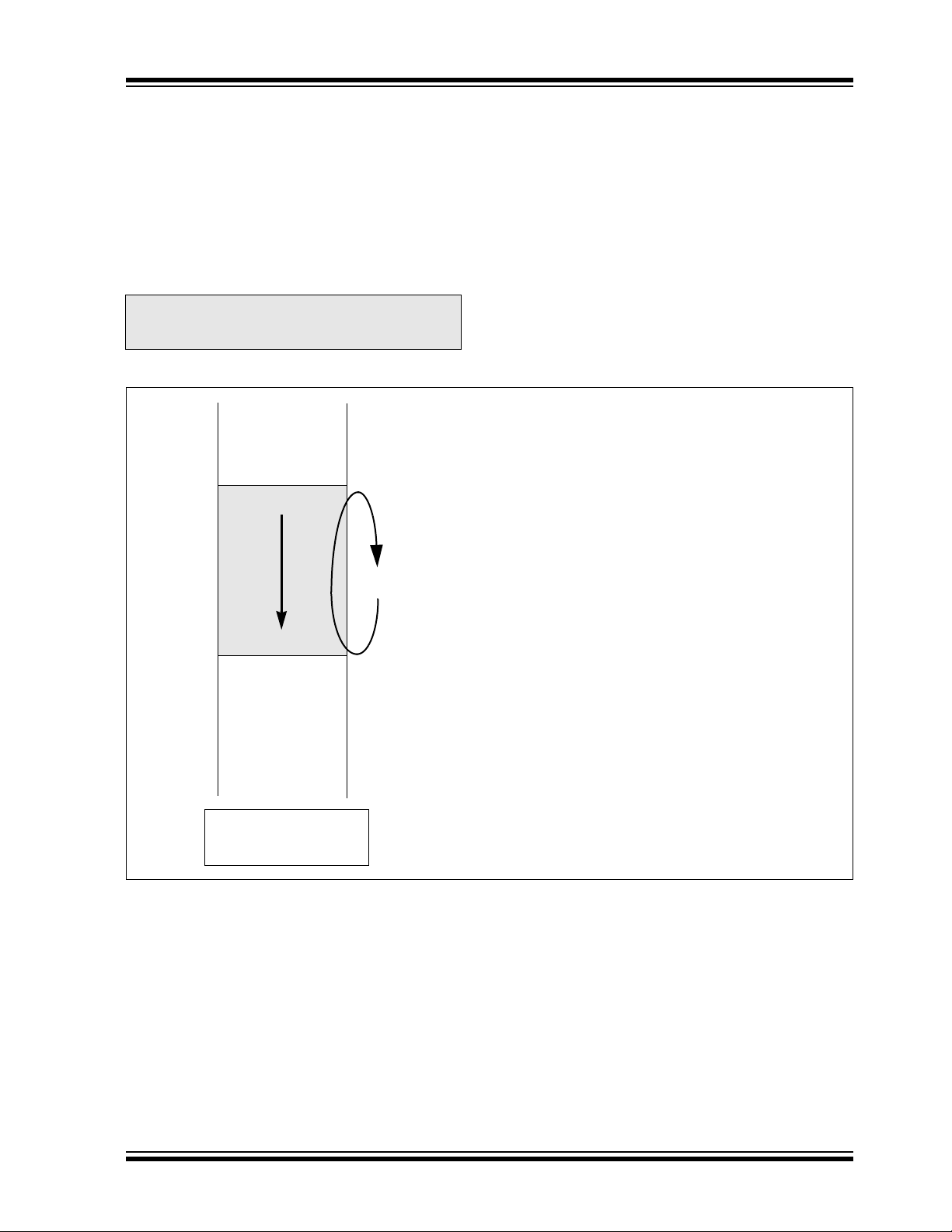
dsPIC30F
4.4.2 W ADDRESS REGISTER
SELECTION
The Modulo and Bit-Reversed Addressing Control register MODCON<15:0> contains enable flags as well as
a W register field to specify the W address registers.
The XWM and YWM fields select which registers will
operate with modulo addressing. If XWM = 15, X
RAGU and X WAGU modulo addressing is disabled.
Similarly, if YWM = 15, Y AGU modulo addressing is
disabled.
Note: The XMODSRT and XMODEND registers
and the XWM register selection are
shared between X RAGU and X WAGU.
The X Address Space Pointer W register (XWM), to
which modulo addressing is to be applied, is stored in
MODCON<3:0> (see Table 3-3). Modulo addressing is
enabled for X data space when XWM is set to any value
other than ‘15’ and the XMODEN bit is set at
MODCON<15>.
The Y Address Space Pointer W register (YWM), to
which modulo addressing is to be applied, is stored in
MODCON<7:4>. Modulo addressing is enabled for Y
data space when YWM is set to any value other than
‘15’ and the YMODEN bit is set at MODCON<14>.
FIGURE 4-1: INCREMENTING BUFFER MODULO ADDRESSING OPERATION EXAMPLE
Byte
Address
0x1100
MOV #0x1100,W0
MOV W0,XMODSRT ;set modulo start address
MOV #0x1163,W0
MOV W0,MODEND ;set modulo end address
MOV #0x8001,W0
MOV W0,MODCON ;enable W1, X AGU for modulo
MOV #0x0000,W0 ;W0 holds buffer fill value
MOV #0x1110,W1 ;point W1 to buffer
0x1163
DO AGAIN,#0x31 ;fill the 50 buffer locations
MOV W0,[W1++] ;fill the next location
AGAIN: INC W0,W0 ;increment the fill value
Start Addr = 0x1100
End Addr = 0x1163
Length = 0x0032 words
2004 Microchip Technology Inc. Preliminary DS70083G-page 51
Page 54
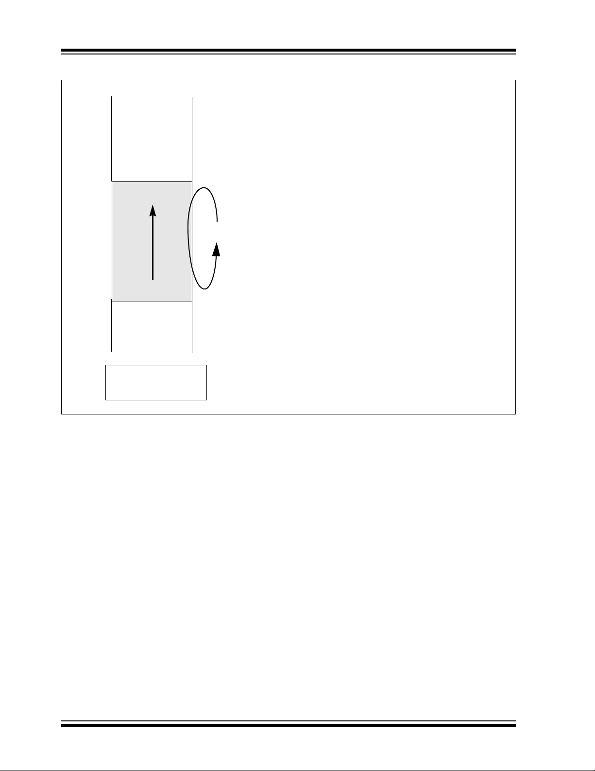
dsPIC30F
FIGURE 4-2: DECREMENTING BUFFER MODULO ADDRESSING OPERATION EXAMPLE
Byte
Address
MOV #0x11D0,W0
MOV #0,XMODSRT ;set modulo start address
MOV 0x11FF,W0
MOV W0,XMODEND ;set modulo end address
MOV #0x8001,W0
MOV W0,MODCON ;enable W1, X AGU for modulo
0x11D0
0x11FF
MOV #0x000F,W0 ;W0 holds buffer fill value
MOV #0x11E0,W1 ;point W1 to buffer
DO AGAIN,#0x17 ;fill the 24 buffer locations
MOV W0,[W1--] ;fill the next location
AGAIN: DEC W0,W0 ; decrement the fill value
Start Addr = 0x11D0
End Addr = 0x11FF
Length = 0x0018 words
DS70083G-page 52 Preliminary 2004 Microchip Technology Inc.
Page 55

dsPIC30F
4.4.3 MODULO ADDRESSING
APPLICABILITY
Modulo addressing can be applied to the effective
address (EA) calculation associated with any W register. It is important to realize that the address boundaries check for addresses less than, or greater than the
upper (for incrementing buffers), and lower (for decrementing buffers) boundary addresses (not just equal
to). Address changes may, therefore, jump over boundaries and still be adjusted correctly (see Section 4.4.4
for restrictions).
Note: The modulo corrected effective address is
written back to the register only when PreModify or Post-Modify Addressing mode is
used to compute the effective address.
When an address offset (e.g., [W7+W2]) is
used, modulo address correction is performed but the contents of the register
remain unchanged.
4.4.4 MODULO ADDRESSING
RESTRICTIONS
For an incrementing buffer, the circular buffer start
address (lower boundary) is arbitrary but must be at a
‘zero’ power-of-two boundary (see Section 4.4.1). For
a decrementing buffer, the circular buffer end address
is arbitrary but must be at a ‘ones’ boundary.
There are no restrictions regarding how much an EA
calculation can exceed the address boundary being
checked and still be successfully corrected.
Once configured, the direction of successive
addresses into a buffer should not be changed.
Although all EAs will continue to be generated correctly, irrespective of offset sign, only one address
boundary is checked for each type of buffer. Thus, if a
buffer is set up to be an incrementing buffer by choosing an appropriate starting address, then correction of
the effective address will be performed by the AGU at
the upper address boundary, but no address correction
will occur if the EA crosses the lower address boundary. Similarly, for a decrementing boundary, address
correction will be performed by the AGU at the lower
address boundary, but no address correction will take
place if the EA crosses the upper address boundary.
The circular buffer pointer may be freely modified in
both directions without a possibility of out-of-range
address access only when the start address satisfies
the condition for an incrementing buffer (last ‘N’ bits are
zeroes) and the end address satisfies the condition for
a decrementing buffer (last ‘N’ bits are ones). Thus, the
modulo addressing capability is truly bidirectional only
for modulo-2 length buffers.
4.5 Bit-Reversed Addressing
Bit-reversed addressing is intended to simplify data reordering for radix-2 FFT algorithms. It is supported by
the X WAGU only (i.e., for data writes only).
The modifier, which may be a constant value or register
contents, is regarded as having its bit order reversed. The
address source and destination are kept in normal order.
Thus, the only operand requiring reversal is the modifier.
4.5.1 BIT-REVERSED ADDRESSING
IMPLEMENTATION
Bit-reversed addressing is enabled when:
1. BWM (W register selection) in the MODCON
register is any value other than ‘15’ (the stack
cannot be accessed using bit-reversed
addressing) and
2. the BREN bit is set in the XBREV register and
3. the Addressing mode used is Register Indirect
with Pre-Increment or Post-Increment.
N
If the length of a bit-reversed buffer is M = 2
then the last ‘N’ bits of the data buffer start address
must be zeros.
XB<14:0> is the bit-reversed address modifier or ‘pivot
point’ which is typically a constant. In the case of an
FFT computation, its value is equal to half of the FFT
data buffer size.
Note: All bit-reversed EA calculations assume
word sized data (LS bit of every EA is
always clear). The XB value is scaled
accordingly to generate compatible (byte)
addresses.
When enabled, bit-reversed addressing will only be
executed for register indirect with pre-increment or
post-increment addressing and word sized data writes.
It will not function for any other Addressing mode or for
byte sized data, and normal addresses will be generated instead. When bit-reversed addressing is active,
the W address pointer will always be added to the
address modifier (XB) and the offset associated with
the Register Indirect Addressing mode will be ignored.
In addition, as word sized data is a requirement, the LS
bit of the EA is ignored (and always clear).
Note: Modulo addressing and bit-reversed
addressing should not be enabled together.
In the event that the user attempts to do
this, bit-reversed addressing will assume
priority when active for the X WAGU, and X
WAGU modulo addressing will be disabled.
However, modulo addressing will continue
to function in the X RAGU.
If bit-reversed addressing has already been enabled by
setting the BREN (XBREV<15>) bit, then a write to the
XBREV register should not be immediately followed by
an indirect read operation using the W register that has
been designated as the bit-reversed pointer.
bytes,
2004 Microchip Technology Inc. Preliminary DS70083G-page 53
Page 56
dsPIC30F
FIGURE 4-3: BIT-REVERSED ADDRESS EXAMPLE
Sequential Address
b15 b14 b13 b12
b11 b10 b9 b8
b7 b6 b5 b4
b3 b2 b1 0
Bit Locations Swapped Left-to-Right
Around Center of Binary Value
b15 b14 b13 b12
b11 b10 b9 b8
b7 b6 b5 b1
b2 b3 b4 0
Bit-Reversed Address
Pivot Point
XB = 0x0008 for a 16-word Bit-Reversed Buffer
TABLE 4-3: BIT-REVERSED ADDRESS SEQUENCE (16-ENTRY)
Normal Address Bit-Reversed Address
A3 A2 A1 A0 Decimal A3 A2 A1 A0 Decimal
0000 0 0000 0
0001 1 1000 8
0010 2 0100 4
0011 3 1100 12
0100 4 0010 2
0101 5 1010 10
0110 6 0110 6
0111 7 1110 14
1000 8 0001 1
1001 9 1001 9
1010 10 0101 5
1011 11 1101 13
1100 12 0011 3
1101 13 1011 11
1110 14 0111 7
1111 15 1111 15
TABLE 4-4: BIT-REVERSED ADDRESS MODIFIER VALUES
Buffer Size (Words) XB<14:0> Bit-Reversed Address Modifier Value
32768 0x4000
16384 0x2000
8192 0x1000
4096 0x0800
2048 0x0400
1024 0x0200
512 0x0100
256 0x0080
128 0x0040
64 0x0020
32 0x0010
16 0x0008
8 0x0004
4 0x0002
2 0x0001
DS70083G-page 54 Preliminary 2004 Microchip Technology Inc.
Page 57

dsPIC30F
5.0 INTERRUPTS
Note: This data sheet summarizes features of this group
of dsPIC30F devices and is not intended to be a complete
reference source. For more information on the CPU,
peripherals, register descriptions and general device
functionality, refer to the dsPIC30F Family Reference
Manual (DS70046). For more information on the device
instruction set and programming, refer to the dsPIC30F
Programmer’s Reference Manual (DS70030).
The dsPIC30F Sensor and General Purpose Family
has up to 41 interrupt sources and 4 processor exceptions (traps) which must be arbitrated based on a
priority scheme.
The CPU is responsible for reading the Interrupt Vector
Table (IVT) and transferring the address contained in
the interrupt vector to the program counter. The interrupt vector is transferred from the program data bus
into the program counter via a 24-bit wide multiplexer
on the input of the program counter.
The Interrupt Vector Table (IVT) and Alternate Interrupt
Vector Table (AIVT) are placed near the beginning of
program memory (0x000004). The IVT and AIVT are
shown in Table 5-2.
The interrupt controller is responsible for preprocessing the interrupts and processor exceptions
prior to them being presented to the processor core.
The peripheral interrupts and traps are enabled, prioritized and controlled using centralized Special Function
Registers:
• IFS0<15:0>, IFS1<15:0>, IFS2<15:0>
All interrupt request flags are maintained in these
three registers. The flags are set by their respective peripherals or external signals, and they are
cleared via software.
• IEC0<15:0>, IEC1<15:0>, IEC2<15:0>
All interrupt enable control bits are maintained in
these three registers. These control bits are used
to individually enable interrupts from the
peripherals or external signals.
• IPC0<15:0>... IPC10<7:0>
The user assignable priority level associated with
each of these 41 interrupts is held centrally in
these twelve registers.
• IPL<3:0>
The current CPU priority level is explicitly stored
in the IPL bits. IPL<3> is present in the CORCON
register, whereas IPL<2:0> are present in the
STATUS register (SR) in the processor core.
• INTCON1<15:0>, INTCON2<15:0>
Global interrupt control functions are derived from
these two registers. INTCON1 contains the control and status flags for the processor exceptions.
The INTCON2 register controls the external
interrupt request signal behavior and the use of
the alternate vector table.
Note: Interrupt flag bits get set when an interrupt
condition occurs, regardless of the state of
its corresponding enable bit. User software should ensure the appropriate interrupt flag bits are clear prior to enabling an
interrupt.
All interrupt sources can be user assigned to one of 7
priority levels, 1 through 7, via the IPCx registers. Each
interrupt source is associated with an interrupt vector,
as shown in Table 5-2. Levels 7 and 1 represent the
highest and lowest maskable priorities, respectively.
Note: Assigning a priority level of ‘0’ to an inter-
rupt source is equivalent to disabling that
interrupt.
If the NSTDIS bit (INTCON1<15>) is set, nesting of
interrupts is prevented. Thus, if an interrupt is currently
being serviced, processing of a new interrupt is prevented even if the new interrupt is of higher priority than
the one currently being serviced.
Note: The IPL bits become read only whenever
the NSTDIS bit has been set to ‘1’.
Certain interrupts have specialized control bits for features like edge or level triggered interrupts, interrupton-change, etc. Control of these features remains
within the peripheral module which generates the
interrupt.
The DISI instruction can be used to disable the processing of interrupts of priorities 6 and lower for a certain number of instructions, during which the DISI bit
(INTCON2<14>) remains set.
When an interrupt is serviced, the PC is loaded with the
address stored in the vector location in program memory that corresponds to the interrupt. There are 63 different vectors within the IVT (refer to Table 5-2). These
vectors are contained in locations 0x000004 through
0x0000FE of program memory (refer to Table 5-2).
These locations contain 24-bit addresses and in order
to preserve robustness, an address error trap will take
place should the PC attempt to fetch any of these
words during normal execution. This prevents execution of random data as a result of accidentally decrementing a PC into vector space, accidentally mapping
a data space address into vector space, or the PC rolling over to 0x000000 after reaching the end of implemented program memory space. Execution of a GOTO
instruction to this vector space will also generate an
address error trap.
2004 Microchip Technology Inc. Preliminary DS70083G-page 55
Page 58

dsPIC30F
5.1 Interrupt Priority
The user assignable interrupt priority (IP<2:0>) bits for
each individual interrupt source are located in the LS
3 bits of each nibble within the IPCx register(s). Bit 3 of
each nibble is not used and is read as a ‘0’. These bits
define the priority level assigned to a particular interrupt
by the user.
Note: The user selectable priority levels start at
0 as the lowest priority and level 7 as the
highest priority.
Since more than one interrupt request source may be
assigned to a specific user specified priority level, a
means is provided to assign priority within a given level.
This method is called “Natural Order Priority”.
Table 5-1 lists the interrupt numbers and interrupt
sources for the dsPIC device and their associated
vector numbers.
Note 1: The natural order priority scheme has 0
as the highest priority and 53 as the
lowest priority.
2: The natural order priority number is the
same as the INT number.
The ability for the user to assign every interrupt to one
of seven priority levels implies that the user can assign
a very high overall priority level to an interrupt with a
low natural order priority. For example, the PLVD (Low
Voltage Detect) can be given a priority of 7. The INT0
(External Interrupt 0) may be assigned to priority level
1, thus giving it a very low effective priority.
TABLE 5-1: NATURAL ORDER PRIORITY
INT
Number
Highest Natural Order Priority
10 18 U1TX - UART1 Transmitter
11 19 ADC - ADC Convert Done
12 20 NVM - NVM Write Complete
13 21 SI2C - I
14 22 MI2C - I
15 23 Input Change Interrupt
16 24 INT1 - External Interrupt 1
17 25 IC7 - Input Capture 7
18 26 IC8 - Input Capture 8
19 27 OC3 - Output Compare 3
20 28 OC4 - Output Compare 4
21 29 T4 - Timer 4
22 30 T5 - Timer 5
23 31 INT2 - External Interrupt 2
24 32 U2RX - UART2 Receiver
25 33 U2TX - UART2 Transmitter
26 34 SPI2
27 35 C1 - Combined IRQ for CAN1
28 36 IC3 - Input Capture 3
29 37 IC4 - Input Capture 4
30 38 IC5 - Input Capture 5
31 39 IC6 - Input Capture 6
32 40 OC5 - Output Compare 5
33 41 OC6 - Output Compare 6
34 42 OC7 - Output Compare 7
35 43 OC8 - Output Compare 8
36 44 INT3 - External Interrupt 3
37 45 INT4 - External Interrupt 4
38 46 C2 - Combined IRQ for CAN2
39-40 47-48 Reserved
41 49 DCI - Codec Transfer Done
42 50 LVD - Low Voltage Detect
43-53 51-61 Reserved
Lowest Natural Order Priority
Vector
Number
0 8 INT0 - External Interrupt 0
1 9 IC1 - Input Capture 1
2 10 OC1 - Output Compare 1
3 11 T1 - Timer 1
4 12 IC2 - Input Capture 2
5 13 OC2 - Output Compare 2
6 14 T2 - Timer 2
7 15 T3 - Timer 3
8 16 SPI1
9 17 U1RX - UART1 Receiver
Interrupt Source
2
C Slave Interrupt
2
C Master Interrupt
DS70083G-page 56 Preliminary 2004 Microchip Technology Inc.
Page 59

dsPIC30F
5.2 Reset Sequence
A Reset is not a true exception, because the interrupt
controller is not involved in the Reset process. The processor initializes its registers in response to a Reset
which forces the PC to zero. The processor then begins
program execution at location 0x000000. A GOTO
instruction is stored in the first program memory location immediately followed by the address target for the
GOTO instruction. The processor executes the GOTO to
the specified address and then begins operation at the
specified target (start) address.
5.2.1 RESET SOURCES
In addition to external Reset and Power-on Reset
(POR), there are 6 sources of error conditions which
‘trap’ to the Reset vector.
• Watchdog Time-out:
The watchdog has timed out, indicating that the
processor is no longer executing the correct flow
of code.
• Uninitialized W Register Trap:
An attempt to use an uninitialized W register as
an address pointer will cause a Reset.
• Illegal Instruction Trap:
Attempted execution of any unused opcodes will
result in an illegal instruction trap. Note that a
fetch of an illegal instruction does not result in an
illegal instruction trap if that instruction is flushed
prior to execution due to a flow change.
• Brown-out Reset (BOR):
A momentary dip in the power supply to the
device has been detected which may result in
malfunction.
• Trap Lockout:
Occurrence of multiple trap conditions
simultaneously will cause a Reset.
5.3 Traps
Traps can be considered as non-maskable, non-stable
interrupts, which adhere to a predefined priority, as
shown in Table 5-2. They are intended to provide the
user a means to correct erroneous operation during
debug and when operating within the application.
Note: If the user does not intend to take correc-
tive action in the event of a trap error condition, these vectors must be loaded with
the address of a default handler that simply contains the RESET instruction. If, on
the other hand, one of the vectors containing an invalid address is called, an
address error trap is generated.
Note that many of these trap conditions can only be
detected when they occur. Consequently, the questionable instruction is allowed to complete prior to trap
exception processing. If the user chooses to recover
from the error, the result of the erroneous action that
caused the trap may have to be corrected.
There are 8 fixed priority levels for traps: level 8 through
level 15, which implies that the IPL3 is always set
during processing of a trap.
If the user is not currently executing a trap, and he sets
the IPL<3:0> bits to a value of ‘0111’ (level 7), then all
interrupts are disabled but traps can still be processed.
5.3.1 TRAP SOURCES
The following traps are provided with increasing priority. However, since all traps can be nested, priority has
little effect.
• Math Error Trap:
The math error trap executes under the following
four circumstances:
1. Should an attempt be made to divide by
zero, the divide operation will be aborted on
a cycle boundary and the trap taken.
2. If enabled, a math error trap will be taken
when an arithmetic operation on either
accumulator A or B causes an overflow
from bit 31 and the accumulator guard bits
are not utilized.
3. If enabled, a math error trap will be taken
when an arithmetic operation on either
accumulator A or B causes a catastrophic
overflow from bit 39 and all saturation is
disabled.
4. If the shift amount specified in a shift
instruction is greater than the maximum
allowed shift amount, a trap will occur.
2004 Microchip Technology Inc. Preliminary DS70083G-page 57
Page 60

dsPIC30F
• Address Error Trap:
This trap is initiated when any of the following
circumstances occurs:
1. A misaligned data word access is
attempted.
2. A data fetch from and unimplemented data
memory location is attempted.
3. A data fetch from an unimplemented program memory location is attempted.
4. An instruction fetch from vector space is
attempted.
Note: In the MAC class of instructions, wherein
the data space is split into X and Y data
space, unimplemented X space includes
all of Y space, and unimplemented Y
space includes all of X space.
5. Execution of a “BRA #literal” instruction or a
“GOTO #literal” instruction, where literal
is an unimplemented program memory address.
6. Executing instructions after modifying the PC to
point to unimplemented program memory
addresses. The PC may be modified by loading
a value into the stack and executing a RETURN
instruction.
• Stack Error Trap:
This trap is initiated under the following
conditions:
1. The stack pointer is loaded with a value
which is greater than the (user programmable) limit value written into the SPLIM
register (stack overflow).
2. The stack pointer is loaded with a value
which is less than 0x0800 (simple stack
underflow).
• Oscillator Fail Trap:
This trap is initiated if the external oscillator fails
and operation becomes reliant on an internal RC
backup.
5.3.2 HARD AND SOFT TRAPS
It is possible that multiple traps can become active
within the same cycle (e.g., a misaligned word stack
write to an overflowed address). In such a case, the
fixed priority shown in Figure 5-2 is implemented,
which may require the user to check if other traps are
pending in order to completely correct the fault.
‘Soft’ traps include exceptions of priority level 8 through
level 11, inclusive. The arithmetic error trap (level 11)
falls into this category of traps. Soft traps can be treated
like non-maskable sources of interrupt that adhere to
the priority assigned by their position in the IVT. Soft
traps are processed like interrupts and require 2 cycles
to be sampled and Acknowledged prior to exception
processing. Therefore, additional instructions may be
executed before a soft trap is Acknowledged.
‘Hard’ traps include exceptions of priority level 12
through level 15, inclusive. The address error (level
12), stack error (level 13) and oscillator error (level 14)
traps fall into this category.
Like soft traps, hard traps can also be viewed as nonmaskable sources of interrupt. The difference between
hard traps and soft traps is that hard traps force the
CPU to stop code execution after the instruction causing the trap has completed. Normal program execution
flow will not resume until after the trap has been
Acknowledged and processed.
If a higher priority trap occurs while any lower priority
trap is in progress, processing of the lower priority trap
will be suspended and the higher priority trap will be
Acknowledged and processed. The lower priority trap
will remain pending until processing of the higher
priority trap completes.
Each hard trap that occurs must be Acknowledged
before code execution of any type may continue. If a
lower priority hard trap occurs while a higher priority
trap is pending, Acknowledged, or is being processed,
a hard trap conflict will occur. The conflict occurs
because the lower priority trap cannot be Acknowledged until processing for the higher priority trap
completes.
The device is automatically reset in a hard trap conflict
condition. The TRAPR status bit (RCON<15>) is set
when the Reset occurs so that the condition may be
detected in software.
In the case of a math error trap or oscillator failure trap,
the condition that causes the trap to occur must be
removed before the respective trap flag bit in the
INTCON1 register may be cleared.
DS70083G-page 58 Preliminary 2004 Microchip Technology Inc.
Page 61

dsPIC30F
5.4 Interrupt Sequence
All interrupt event flags are sampled in the beginning of
each instruction cycle by the IFSx registers. A pending
interrupt request (IRQ) is indicated by the flag bit being
equal to a ‘1’ in an IFSx register. The IRQ will cause an
interrupt to occur if the corresponding bit in the Interrupt
Enable (IECx) register is set. For the remainder of the
instruction cycle, the priorities of all pending interrupt
requests are evaluated.
If there is a pending IRQ with a priority level greater
than the current processor priority level in the IPL bits,
the processor will be interrupted.
The processor then stacks the current program counter
and the low byte of the processor STATUS register
(SRL), as shown in Figure 5-1. The low byte of the
STATUS register contains the processor priority level at
the time prior to the beginning of the interrupt cycle.
The processor then loads the priority level for this interrupt into the STATUS register. This action will disable
all lower priority interrupts until the completion of the
Interrupt Service Routine.
FIGURE 5-1: INTERRUPT STACK
FRAME
0x0000
PC<15:0>
SRL IPL3 PC<22:16>
<Free Word>
Higher Address
Stack Grows Towards
Note 1: The user can always lower the priority
level by writing a new value into SR. The
Interrupt Service Routine must clear the
interrupt flag bits in the IFSx register
before lowering the processor interrupt
priority, in order to avoid recursive
interrupts.
2: The IPL3 bit (CORCON<3>) is always
clear when interrupts are being processed. It is set only during execution of
traps.
The RETFIE (return from interrupt) instruction will
unstack the program counter and STATUS registers to
return the processor to its state prior to the interrupt
sequence.
015
W15 (before CALL)
W15 (after CALL)
POP : [--W15]
PUSH: [W15++]
FIGURE 5-2: EXCEPTION VECTORS
IVT
Priority
Decreasing
AIVT
Reset - GOTO Instruction
Reset - GOTO Address
Reserved
Oscillator Fail Trap Vector
Address Error Trap Vector
Stack Error Trap Vector
Math Error Trap Vector
Reserved Vector
Reserved Vector
Reserved Vector
Interrupt 0 Vector
Interrupt 1 Vector
~
~
~
Interrupt 52 Vector
Interrupt 53 Vector
Reserved
Reserved
Reserved
Oscillator Fail Trap Vector
Stack Error Trap Vector
Address Error Trap Vector
Math Error Trap Vector
Reserved Vector
Reserved Vector
Reserved Vector
Interrupt 0 Vector
Interrupt 1 Vector
~
~
~
Interrupt 52 Vector
Interrupt 53 Vector
0x000000
0x000002
0x000004
0x000014
0x00007E
0x000080
0x000082
0x000084
0x000094
0x0000FE
5.5 Alternate Vector Table
In program memory, the Interrupt Vector Table (IVT) is
followed by the Alternate Interrupt Vector Table (AIVT),
as shown in Table 5-2. Access to the alternate vector
table is provided by the ALTIVT bit in the INTCON2 register. If the ALTIVT bit is set, all interrupt and exception
processes will use the alternate vectors instead of the
default vectors. The alternate vectors are organized in
the same manner as the default vectors. The AIVT supports emulation and debugging efforts by providing a
means to switch between an application and a support
environment without requiring the interrupt vectors to
be reprogrammed. This feature also enables switching
between applications for evaluation of different
software algorithms at run time.
If the AIVT is not required, the program memory allocated to the AIVT may be used for other purposes.
AIVT is not a protected section and may be freely
programmed by the user.
2004 Microchip Technology Inc. Preliminary DS70083G-page 59
Page 62

dsPIC30F
5.6 Fast Context Saving
A context saving option is available using shadow registers. Shadow registers are provided for the DC, N,
OV, Z and C bits in SR, and the registers W0 through
W3. The shadows are only one level deep. The shadow
registers are accessible using the PUSH.S and POP.S
instructions only.
When the processor vectors to an interrupt, the
PUSH.S instruction can be used to store the current
value of the aforementioned registers into their
respective shadow registers.
If an ISR of a certain priority uses the PUSH.S and
POP.S instructions for fast context saving, then a
higher priority ISR should not include the same instructions. Users must save the key registers in software
during a lower priority interrupt if the higher priority ISR
uses fast context saving.
5.7 External Interrupt Requests
The interrupt controller supports up to five external
interrupt request signals, INT0-INT4. These inputs are
edge sensitive; they require a low-to-high or a high-tolow transition to generate an interrupt request. The
INTCON2 register has five bits, INT0EP-INT4EP, that
select the polarity of the edge detection circuitry.
5.8 Wake-up from Sleep and Idle
The interrupt controller may be used to wake-up the
processor from either Sleep or Idle modes, if Sleep or
Idle mode is active when the interrupt is generated.
If an enabled interrupt request of sufficient priority is
received by the interrupt controller, then the standard
interrupt request is presented to the processor. At the
same time, the processor will wake-up from Sleep or
Idle and begin execution of the Interrupt Service
Routine (ISR) needed to process the interrupt request.
DS70083G-page 60 Preliminary 2004 Microchip Technology Inc.
Page 63

dsPIC30F
0000 0000 0000 0000
0000 0000 0000 0000
0000 0000 0000 0000
0000 0000 0000 0000
0000 0000 0000 0000
0000 0000 0000 0000
0000 0000 0000 0000
0100 0100 0100 0100
0100 0100 0100 0100
0100 0100 0100 0100
0000 0000 0000 0000
0100 0100 0100 0100
0100 0100 0100 0100
0100 0100 0100 0100
0100 0100 0100 0100
0100 0100 0100 0100
0100 0100 0100 0100
0000 0100 0100 0100
0000 0100 0100 0000
— — — — OVATE OVBTE COVTE — — — MATHERR ADDRERR STKERR OSCFAIL —
— — — — — — — — — — INT4EP INT3EP INT2EP INT1EP INT0EP
— — — — — LVDIF DCIIF — — C2IF INT4IF INT3IF OC8IF OC7IF OC6IF OC5IF
ADR Bit 15 Bit 14 Bit 13 Bit 12 Bit 11 Bit 10 Bit 9 Bit 8 Bit 7 Bit 6 Bit 5 Bit 4 Bit 3 Bit 2 Bit 1 Bit 0 Reset State
SFR
Name
INTCON1 0080 NSTDIS
IFS0 0084 CNIF MI2CIF SI2CIF NVMIF ADIF U1TXIF U1RXIF SPI1IF T3IF T2IF OC2IF IC2IF T1IF OC1IF IC1IF INT0IF
IFS1 0086 IC6IF IC5IF IC4IF IC3IF C1IF SPI2IF U2TXIF U2RXIF INT2IF T5IF T4IF OC4IF OC3IF IC8IF IC7IF INT1IF
TABLE 5-2: INTERRUPT CONTROLLER REGISTER MAP
INTCON2 0082 ALTIVT
IFS2 0088
IEC0 008C CNIE MI2CIE SI2CIE NVMIE ADIE U1TXIE U1RXIE SPI1IE T3IE T2IE OC2IE IC2IE T1IE OC1IE IC1IE INT0IE
— — — — — LVDIE DCIIE — — C2IE INT4IE INT3IE OC8IE OC7IE OC6IE OC5IE
IEC1 008E IC6IE IC5IE IC4IE IC3IE C1IE SPI2IE U2TXIE U2RXIE INT2IE T5IE T4IE OC4IE OC3IE IC8IE IC7IE INT1IE
IEC2 0090
— T1IP<2:0> — OC1IP<2:0> — IC1IP<2:0> — INT0IP<2:0>
— T31P<2:0> — T2IP<2:0> — OC2IP<2:0> — IC2IP<2:0>
— ADIP<2:0> — U1TXIP<2:0> — U1RXIP<2:0> — SPI1IP<2:0>
IPC0 0094
IPC1 0096
IPC2 0098
— CNIP<2:0> — MI2CIP<2:0> — SI2CIP<2:0> — NVMIP<2:0>
— OC3IP<2:0> — IC8IP<2:0> — IC7IP<2:0> — INT1IP<2:0>
— INT2IP<2:0> — T5IP<2:0> — T4IP<2:0> — OC4IP<2:0>
IPC3 009A
IPC4 009C
IPC5 009E
— C1IP<2:0> — SPI2IP<2:0> — U2TXIP<2:0> — U2RXIP<2:0>
— IC6IP<2:0> — IC5IP<2:0> — IC4IP<2:0> — IC3IP<2:0>
— OC8IP<2:0> — OC7IP<2:0> — OC6IP<2:0> — OC5IP<2:0>
IPC6 00A0
IPC7 00A2
IPC8 00A4
— — — — — C2IP<2:0> — INT41IP<2:0> — INT3IP<2:0>
— — — — — LVDIP<2:0> — DCIIP<2:0> — — — —
IPC9 00A6
IPC10 00A8
Legend: u = uninitialized bit
Note: Refer to dsPIC30F Family Reference Manual (DS70046) for descriptions of register bit fields.
2004 Microchip Technology Inc. Preliminary DS70083G-page 61
Page 64

dsPIC30F
NOTES:
DS70083G-page 62 Preliminary 2004 Microchip Technology Inc.
Page 65
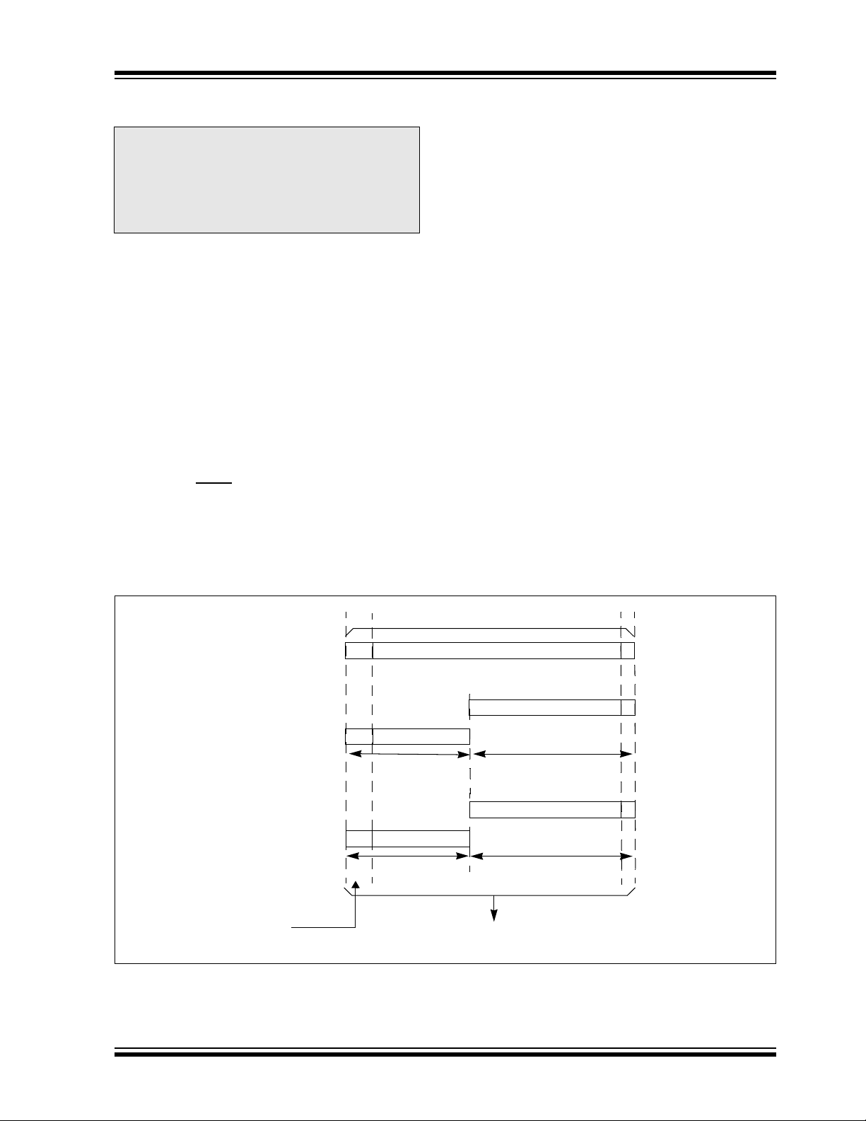
dsPIC30F
6.0 FLASH PROGRAM MEMORY
Note: This data sheet summarizes features of this group
of dsPIC30F devices and is not intended to be a complete
reference source. For more information on the CPU,
peripherals, register descriptions and general device
functionality, refer to the dsPIC30F Family Reference
Manual (DS70046). For more information on the device
instruction set and programming, refer to the dsPIC30F
Programmer’s Reference Manual (DS70030).
The dsPIC30F family of devices contains internal program Flash memory for executing user code. There are
two methods by which the user can program this
memory:
1. Run-Time Self-Programming (RTSP)
2. In-Circuit Serial Programming™ (ICSP™)
6.1 In-Circuit Serial Programming (ICSP)
dsPIC30F devices can be serially programmed while in
the end application circuit. This is simply done with two
lines for Programming Clock and Programming Data
(which are named PGC and PGD respectively), and
three other lines for Power (V
Master Clear (MCLR
). this allows customers to manufacture boards with unprogrammed devices, and then
program the microcontroller just before shipping the
product. This also allows the most recent firmware or a
custom firmware to be programmed.
DD), Ground (VSS) and
6.2 Run-Time Self-Programming (RTSP)
RTSP is accomplished using TBLRD (table read) and
TBLWT (table write) instructions. With RTSP, the user
may erase and program 32 instructions (96 bytes) at a
time.
6.3 Table Instruction Operation Summary
The TBLRDL and the TBLWTL instructions are used to
read or write to bits<15:0> of program memory.
TBLRDL and TBLWTL can access program memory in
Word or Byte mode.
The TBLRDH and TBLWTH instructions are used to read
or write to bits<23:16> of program memory. TBLRDH
and TBLWTH can access program memory in Word or
Byte mode.
A 24-bit program memory address is formed using
bits<7:0> of the TBLPAG register and the effective
address (EA) from a W register specified in the table
instruction, as shown in Figure 6-1.
FIGURE 6-1: ADDRESSING FOR TABLE AND NVM REGISTERS
24 bits
Using
Program
Counter
Using
NVMADR
Addressing
Using
Table
Instruction
User/Configuration
Space Select
0
1/0
NVMADRU Reg
1/0
TBLPAG Reg
8 bits 16 bits
8 bits
Program Counter
NVMADR Reg EA
Working Reg EA
16 bits
24-bit EA
0
Byte
Select
2004 Microchip Technology Inc. Preliminary DS70083G-page 63
Page 66

dsPIC30F
6.4 RTSP Operation
The dsPIC30F Flash program memory is organized
into rows and panels. Each row consists of 32 instructions or 96 bytes. Each panel consists of 128 rows or
4K x 24 instructions. RTSP allows the user to erase and
program one row (32 instructions) at a time. RTSP may
be used to program multiple program memory panels,
but the table pointer must be changed at each panel
boundary.
Each panel of program memory contains write latches
that hold 32 instructions of programming data. Prior to
the actual programming operation, the write data must
be loaded into the panel write latches. The data to be
programmed into the panel is loaded in sequential
order into the write latches: instruction 0, instruction 1,
etc. The instruction words loaded must always be from
a group of 32 boundary.
The basic sequence for RTSP programming is to set up
a table pointer, then do a series of TBLWT instructions
to load the write latches. Programming is performed by
setting the special bits in the NVMCON register. Four
TBLWTL and four TBLWTH instructions are required to
load the four instructions. To fully program a row of
program memory, eight cycles of four TBLWTL and four
TBLWTH are required. If multiple panel programming
is required, the table pointer needs to be changed and
the next set of multiple write latches written.
All of the table write operations are single word writes
(2 instruction cycles) because only the table latches are
written. A total of 32 programming passes, each writing
4 instruction words, are required per row.
The Flash program memory is readable, writable, and
erasable during normal operation over the entire V
range.
DD
6.5 Control Registers
The four SFRs used to read and write the program
Flash memory are:
•NVMCON
•NVMADR
• NVMADRU
•NVMKEY
6.5.1 NVMCON REGISTER
The NVMCON register controls which blocks are to be
erased, which memory type is to be programmed and
start of the programming cycle.
6.5.2 NVMADR REGISTER
The NVMADR register is used to hold the lower two
bytes of the effective address. The NVMADR register
captures the EA<15:0> of the last table instruction that
has been executed and selects the row to write.
6.5.3 NVMADRU REGISTER
The NVMADRU register is used to hold the upper byte
of the effective address. The NVMADRU register captures the EA<23:16> of the last table instruction that
has been executed.
6.5.4 NVMKEY REGISTER
NVMKEY is a write only register that is used for write
protection. To start a programming or an erase
sequence, the user must consecutively write 0x55 and
0xAA to the NVMKEY register. Refer to Section 6.6 for
further details.
DS70083G-page 64 Preliminary 2004 Microchip Technology Inc.
Page 67

dsPIC30F
6.6 Programming Operations
A complete programming sequence is necessary for
programming or erasing the internal Flash in RTSP
mode. A programming operation is nominally 2 msec in
duration and the processor stalls (waits) until the operation is finished. Setting the WR bit (NVMCON<15>)
starts the operation, and the WR bit is automatically
cleared when the operation is finished.
6.6.1 PROGRAMMING ALGORITHM FOR
PROGRAM FLASH
The user can erase one row of program Flash memory
at a time. The user can program one block
(4 instruction words) of Flash memory at a time. The
general process is:
1. Read one row of program Flash (32 instruction
words) and store into data RAM as a data
“image”.
2. Update the data image with the desired new
data.
3. Erase program Flash row.
a) Setup NVMCON register for multi-word,
program Flash, erase, and set WREN bit.
b) Write address of row to be erased into
NVMADRU/NVMADR.
c) Write ‘55’ to NVMKEY.
d) Write ‘AA’ to NVMKEY.
e) Set the WR bit. This will begin erase cycle.
f) CPU will stall for the duration of the erase
cycle.
g) The WR bit is cleared when erase cycle
ends.
4. Write 32 instruction words of data from data
RAM into the program Flash write latches.
5. Program 32 instruction words into program
Flash.
a) Setup NVMCON register for multi-word,
program Flash, program, and set WREN
bit.
b) Write ‘55’ to NVMKEY.
c) Write ‘AA’ to NVMKEY.
d) Set the WR bit. This will begin program
cycle.
e) CPU will stall for duration of the program
cycle.
f) The WR bit is cleared by the hardware
when program cycle ends.
6. Repeat steps 1 through 5 as needed to program
desired amount of program Flash memory.
6.6.2 ERASING A ROW OF PROGRAM
MEMORY
Example 6-1 shows a code sequence that can be used
to erase a row (32 instructions) of program memory.
EXAMPLE 6-1: ERASING A ROW OF PROGRAM MEMORY
; Setup NVMCON for erase operation, multi word write
; program memory selected, and writes enabled
MOV #0x4041,W0 ;
MOV W0
; Init pointer to row to be ERASED
MOV #tblpage(PROG_ADDR),W0 ;
MOV W0
MOV #tbloffset(PROG_ADDR),W0 ; Intialize in-page EA[15:0] pointer
MOV W0, NVMADR ; Initialize NVMADR SFR
DISI #5 ; Block all interrupts with priority <7 for
MOV #0x55,W0
MOV W0
MOV #0xAA,W1 ;
MOV W1
BSET NVMCON,#WR ; Start the erase sequence
NOP ; Insert two NOPs after the erase
NOP ; command is asserted
2004 Microchip Technology Inc. Preliminary DS70083G-page 65
NVMCON ; Init NVMCON SFR
,
NVMADRU ; Initialize PM Page Boundary SFR
,
; next 5 instructions
NVMKEY ; Write the 0x55 key
,
NVMKEY ; Write the 0xAA key
,
Page 68

dsPIC30F
6.6.3 LOADING WRITE LATCHES
Example 6-2 shows a sequence of instructions that can
be used to load the 96 bytes of write latches. Four
TBLWTL and four TBLWTH instructions are needed to
load the write latches selected by the table pointer.
EXAMPLE 6-2: LOADING WRITE LATCHES
; Set up a pointer to the first program memory location to be written
; program memory selected, and writes enabled
MOV #0x0000,W0 ;
MOV W0
MOV #0x6000,W0 ; An example program memory address
; Perform the TBLWT instructions to write the latches
; 0th_program_word
MOV #LOW_WORD_0,W2 ;
MOV #HIGH_BYTE_0,W3 ;
TBLWTL W2
TBLWTH W3
; 1st_program_word
MOV #LOW_WORD_1,W2 ;
MOV #HIGH_BYTE_1,W3 ;
TBLWTL W2
TBLWTH W3
; 2nd_program_word
MOV #LOW_WORD_2,W2 ;
MOV #HIGH_BYTE_2,W3 ;
TBLWTL W2
TBLWTH W3
•
•
•
; 31st_program_word
MOV #LOW_WORD_3,W2 ;
MOV #HIGH_BYTE_3,W3 ;
TBLWTL W2
TBLWTH W3
TBLPAG ; Initialize PM Page Boundary SFR
,
[W0] ; Write PM low word into program latch
,
[W0++] ; Write PM high byte into program latch
,
[W0] ; Write PM low word into program latch
,
[W0++] ; Write PM high byte into program latch
,
[W0] ; Write PM low word into program latch
,
[W0++] ; Write PM high byte into program latch
,
[W0] ; Write PM low word into program latch
,
[W0++] ; Write PM high byte into program latch
,
Note: In Example 6-2, the contents of the upper byte of W3 has no effect.
6.6.4 INITIATING THE PROGRAMMING
SEQUENCE
For protection, the write initiate sequence for NVMKEY
must be used to allow any erase or program operation
to proceed. After the programming command has been
executed, the user must wait for the programming time
until programming is complete. The two instructions following the start of the programming sequence should
be NOPs.
EXAMPLE 6-3: INITIATING A PROGRAMMING SEQUENCE
DISI #5 ; Block all interrupts with priority <7 for
MOV #0x55,W0 ;
MOV W0
MOV #0xAA,W1 ;
MOV W1
BSET NVMCON,#WR ; Start the erase sequence
NOP ; Insert two NOPs after the erase
NOP ; command is asserted
NVMKEY ; Write the 0x55 key
,
NVMKEY ; Write the 0xAA key
,
; next 5 instructions
DS70083G-page 66 Preliminary 2004 Microchip Technology Inc.
Page 69
dsPIC30F
— — — — — — — — NVMADR<23:16> 0000 0000 uuuu uuuu
— — — — — — — — KEY<7:0> 0000 0000 0000 0000
File Name Addr. Bit 15 Bit 14 Bit 13 Bit 12 Bit 11 Bit 10 Bit 9 Bit 8 Bit 7 Bit 6 Bit 5 Bit 4 Bit 3 Bit 2 Bit 1 Bit 0 All RESETS
NVMCON 0760 WR WREN WRERR — — — — TWRI — PROGOP<6:0> 0000 0000 0000 0000
TABLE 6-1: NVM REGISTER MAP
2004 Microchip Technology Inc. Preliminary DS70083G-page 67
NVMKEY 0766
NVMADRU 0764
Legend: u = uninitialized bit
Note: Refer to dsPIC30F Family Reference Manual (DS70046) for descriptions of register bit fields.
NVMADR 0762 NVMADR<15:0> uuuu uuuu uuuu uuuu
Page 70

dsPIC30F
NOTES:
DS70083G-page 68 Preliminary 2004 Microchip Technology Inc.
Page 71

dsPIC30F
7.0 DATA EEPROM MEMORY
Note: This data sheet summarizes features of this group
of dsPIC30F devices and is not intended to be a complete
reference source. For more information on the CPU,
peripherals, register descriptions and general device
functionality, refer to the dsPIC30F Family Reference
Manual (DS70046). For more information on the device
instruction set and programming, refer to the dsPIC30F
Programmer’s Reference Manual (DS70030).
The Data EEPROM Memory is readable and writable
during normal operation over the entire V
data EEPROM memory is directly mapped in the
program memory address space.
The four SFRs used to read and write the program
Flash memory are used to access data EEPROM
memory, as well. As described in Section 6.5, these
registers are:
•NVMCON
•NVMADR
• NVMADRU
•NVMKEY
The EEPROM data memory allows read and write of
single words and 16-word blocks. When interfacing to
data memory, NVMADR in conjunction with the
NVMADRU register are used to address the EEPROM
location being accessed. TBLRDL and TBLWTL
instructions are used to read and write data EEPROM.
The dsPIC30F devices have up to 8 Kbytes (4K
words) of data EEPROM with an address range from
0x7FF000 to 0x7FFFFE.
A word write operation should be preceded by an erase
of the corresponding memory location(s). The write typically requires 2 ms to complete but the write time will
vary with voltage and temperature.
A program or erase operation on the data EEPROM
does not stop the instruction flow. The user is responsible for waiting for the appropriate duration of time
before initiating another data EEPROM write/erase
operation. Attempting to read the data EEPROM while
a programming or erase operation is in progress results
in unspecified data.
DD range. The
Control bit WR initiates write operations similar to program Flash writes. This bit cannot be cleared, only set,
in software. They are cleared in hardware at the completion of the write operation. The inability to clear the
WR bit in software prevents the accidental or
premature termination of a write operation.
The WREN bit, when set, will allow a write operation.
On power-up, the WREN bit is clear. The WRERR bit is
set when a write operation is interrupted by a MCLR
Reset or a WDT Time-out Reset during normal operation. In these situations, following Reset, the user can
check the WRERR bit and rewrite the location. The
address register NVMADR remains unchanged.
Note: Interrupt flag bit NVMIF in the IFS0 regis-
ter is set when write is complete. It must be
cleared in software.
7.1 Reading the Data EEPROM
A TBLRD instruction reads a word at the current program word address. This example uses W0 as a
pointer to data EEPROM. The result is placed in
register W4 as shown in Example 7-1.
EXAMPLE 7-1: DATA EEPROM READ
MOV #LOW_ADDR_WORD,W0 ; Init Pointer
MOV #HIGH_ADDR_WORD,W1
MOV W1
TBLRDL [ W0 ], W4 ; read data EEPROM
TBLPAG
,
2004 Microchip Technology Inc. Preliminary DS70083G-page 69
Page 72

dsPIC30F
7.2 Erasing Data EEPROM
7.2.1 ERASING A BLOCK OF DATA
EEPROM
In order to erase a block of data EEPROM, the
NVMADRU and NVMADR registers must initially point
to the block of memory to be erased. Configure
NVMCON for erasing a block of data EEPROM, and
set the ERASE and WREN bits in the NVMCON
register. Setting the WR bit initiates the erase as
shown in Example 7-2.
EXAMPLE 7-2: DATA EEPROM BLOCK ERASE
; Select data EEPROM block, ERASE, WREN bits
MOV #4045,W0
MOV W0
; Start erase cycle by setting WR after writing key sequence
DISI #5 ; Block all interrupts with priority <7 for
MOV #0x55,W0 ;
MOV W0
MOV #0xAA,W1 ;
MOV W1
BSET NVMCON,#WR ; Initiate erase sequence
NOP
NOP
; Erase cycle will complete in 2mS. CPU is not stalled for the Data Erase Cycle
; User can poll WR bit, use NVMIF or Timer IRQ to determine erasure complete
NVMCON ; Initialize NVMCON SFR
,
; next 5 instructions
NVMKEY ; Write the 0x55 key
,
NVMKEY ; Write the 0xAA key
,
7.2.2 ERASING A WORD OF DATA
EEPROM
The TBLPAG and NVMADR registers must point to the
block. Select erase a block of data Flash, and set the
ERASE and WREN bits in the NVMCON register. Setting the WR bit initiates the erase as shown in
Example 7-3.
EXAMPLE 7-3: DATA EEPROM WORD ERASE
; Select data EEPROM word, ERASE, WREN bits
MOV #4044,W0
MOV W0
; Start erase cycle by setting WR after writing key sequence
DISI #5 ; Block all interrupts with priority <7 for
MOV #0x55,W0 ;
MOV W0
MOV #0xAA,W1 ;
MOV W1
BSET NVMCON,#WR ; Initiate erase sequence
NOP
NOP
; Erase cycle will complete in 2mS. CPU is not stalled for the Data Erase Cycle
; User can poll WR bit, use NVMIF or Timer IRQ to determine erasure complete
NVMCON
,
; next 5 instructions
NVMKEY ; Write the 0x55 key
,
NVMKEY ; Write the 0xAA key
,
DS70083G-page 70 Preliminary 2004 Microchip Technology Inc.
Page 73

dsPIC30F
7.3 Writing to the Data EEPROM
To write an EEPROM data location, the following
sequence must be followed:
1. Erase data EEPROM word.
a) Select word, data EEPROM erase, and set
WREN bit in NVMCON register.
b) Write address of word to be erased into
NVMADR.
c) Enable NVM interrupt (optional).
d) Write ‘55’ to NVMKEY.
e) Write ‘AA’ to NVMKEY.
f) Set the WR bit. This will begin erase cycle.
g) Either poll NVMIF bit or wait for NVMIF
interrupt.
h) The WR bit is cleared when the erase cycle
ends.
2. Write data word into data EEPROM write
latches.
3. Program 1 data word into data EEPROM.
a) Select word, data EEPROM program, and
set WREN bit in NVMCON register.
b) Enable NVM write done interrupt (optional).
c) Write ‘55’ to NVMKEY.
d) Write ‘AA’ to NVMKEY.
e) Set the WR bit. This will begin program
cycle.
f) Either poll NVMIF bit or wait for NVM
interrupt.
g) The WR bit is cleared when the write cycle
ends.
The write will not initiate if the above sequence is not
exactly followed (write 0x55 to NVMKEY, write 0xAA to
NVMCON, then set WR bit) for each word. It is strongly
recommended that interrupts be disabled during this
code segment.
Additionally, the WREN bit in NVMCON must be set to
enable writes. This mechanism prevents accidental
writes to data EEPROM due to unexpected code execution. The WREN bit should be kept clear at all times
except when updating the EEPROM. The WREN bit is
not cleared by hardware.
After a write sequence has been initiated, clearing the
WREN bit will not affect the current write cycle. The WR
bit will be inhibited from being set unless the WREN bit
is set. The WREN bit must be set on a previous instruction. Both WR and WREN cannot be set with the same
instruction.
At the completion of the write cycle, the WR bit is
cleared in hardware and the Non-Volatile Memory
Write Complete Interrupt Flag bit (NVMIF) is set. The
user may either enable this interrupt or poll this bit.
NVMIF must be cleared by software.
7.3.1 WRITING A WORD OF DATA
EEPROM
Once the user has erased the word to be programmed,
then a table write instruction is used to write one write
latch, as shown in Example 7-4.
EXAMPLE 7-4: DATA EEPROM WORD WRITE
; Point to data memory
MOV #LOW_ADDR_WORD,W0 ; Init pointer
MOV #HIGH_ADDR_WORD,W1
MOV W1
MOV #LOW(WORD),W2 ; Get data
TBLWTL W2
; The NVMADR captures last table access address
; Select data EEPROM for 1 word op
MOV #0x4004,W0
MOV W0
; Operate key to allow write operation
DISI #5 ; Block all interrupts with priority <7 for
MOV #0x55,W0
MOV W0
MOV #0xAA,W1
MOV W1
BSET NVMCON,#WR ; Initiate program sequence
NOP
NOP
; Write cycle will complete in 2mS. CPU is not stalled for the Data Write Cycle
; User can poll WR bit, use NVMIF or Timer IRQ to determine write complete
2004 Microchip Technology Inc. Preliminary DS70083G-page 71
TBLPAG
,
[ W0] ; Write data
,
NVMCON
,
; next 5 instructions
NVMKEY ; Write the 0x55 key
,
NVMKEY ; Write the 0xAA key
,
Page 74

dsPIC30F
7.3.2 WRITING A BLOCK OF DATA
EEPROM
To write a block of data EEPROM, write to all sixteen
latches first, then set the NVMCON register and
program the block.
EXAMPLE 7-5: DATA EEPROM BLOCK WRITE
MOV #LOW_ADDR_WORD,W0 ; Init pointer
MOV #HIGH_ADDR_WORD,W1
MOV W1
MOV #data1,W2 ; Get 1st data
TBLWTL W2
MOV #data2,W2 ; Get 2nd data
TBLWTL W2
MOV #data3,W2 ; Get 3rd data
TBLWTL W2
MOV #data4,W2 ; Get 4th data
TBLWTL W2
MOV #data5,W2 ; Get 5th data
TBLWTL W2
MOV #data6,W2 ; Get 6th data
TBLWTL W2
MOV #data7,W2 ; Get 7th data
TBLWTL W2
MOV #data8,W2 ; Get 8th data
TBLWTL W2
MOV #data9,W2 ; Get 9th data
TBLWTL W2
MOV #data10,W2 ; Get 10th data
TBLWTL W2
MOV #data11,W2 ; Get 11th data
TBLWTL W2
MOV #data12,W2 ; Get 12th data
TBLWTL W2
MOV #data13,W2 ; Get 13th data
TBLWTL W2
MOV #data14,W2 ; Get 14th data
TBLWTL W2
MOV #data15,W2 ; Get 15th data
TBLWTL W2
MOV #data16,W2 ; Get 16th data
TBLWTL W2
MOV #0x400A,W0 ; Select data EEPROM for multi word op
MOV W0
DISI #5 ; Block all interrupts with priority <7 for
MOV #0x55,W0
MOV W0
MOV #0xAA,W1
MOV W1
BSET NVMCON,#WR ; Start write cycle
NOP
NOP
TBLPAG
,
[ W0]++ ; write data
,
[ W0]++ ; write data
,
[ W0]++ ; write data
,
[ W0]++ ; write data
,
[ W0]++ ; write data
,
[ W0]++ ; write data
,
[ W0]++ ; write data
,
[ W0]++ ; write data
,
[ W0]++ ; write data
,
[ W0]++ ; write data
,
[ W0]++ ; write data
,
[ W0]++ ; write data
,
[ W0]++ ; write data
,
[ W0]++ ; write data
,
[ W0]++ ; write data
,
[ W0]++ ; write data. The NVMADR captures last table access address.
,
NVMCON ; Operate Key to allow program operation
,
; next 5 instructions
NVMKEY ; Write the 0x55 key
,
NVMKEY ; Write the 0xAA key
,
DS70083G-page 72 Preliminary 2004 Microchip Technology Inc.
Page 75

dsPIC30F
7.4 Write Verify
Depending on the application, good programming
practice may dictate that the value written to the memory should be verified against the original value. This
should be used in applications where excessive writes
can stress bits near the specification limit.
7.5 Protection Against Spurious Write
There are conditions when the device may not want to
write to the data EEPROM memory. To protect against
spurious EEPROM writes, various mechanisms have
been built-in. On power-up, the WREN bit is cleared;
also, the Power-up Timer prevents EEPROM write.
The write initiate sequence and the WREN bit together
help prevent an accidental write during brown-out,
power glitch, or software malfunction.
2004 Microchip Technology Inc. Preliminary DS70083G-page 73
Page 76

dsPIC30F
NOTES:
DS70083G-page 74 Preliminary 2004 Microchip Technology Inc.
Page 77

dsPIC30F
8.0 I/O PORTS
Note: This data sheet summarizes features of this group
of dsPIC30F devices and is not intended to be a complete
reference source. For more information on the CPU,
peripherals, register descriptions and general device
functionality, refer to the dsPIC30F Family Reference
Manual (DS70046).
All of the device pins (except VDD, VSS, MCLR, and
OSC1/CLKI) are shared between the peripherals and
the parallel I/O ports.
All I/O input ports feature Schmitt Trigger inputs for
improved noise immunity.
8.1 Parallel I/O (PIO) Ports
When a peripheral is enabled and the peripheral is
actively driving an associated pin, the use of the pin as
a general purpose output pin is disabled. The I/O pin
may be read but the output driver for the parallel port bit
will be disabled. If a peripheral is enabled but the
peripheral is not actively driving a pin, that pin may be
driven by a port.
All port pins have three registers directly associated
with the operation of the port pin. The Data Direction
register (TRISx) determines whether the pin is an input
or an output. If the data direction bit is a ‘1’, then the pin
is an input. All port pins are defined as inputs after a
Reset. Reads from the latch (LATx), read the latch.
Writes to the latch, write the latch (LATx). Reads from
the port (PORTx), read the port pins and writes to the
port pins, write the latch (LATx).
Any bit and its associated data and control registers
that are not valid for a particular device will be disabled. That means the corresponding LATx and TRISx
registers and the port pin will read as zeros.
When a pin is shared with another peripheral or function that is defined as an input only, it is nevertheless
regarded as a dedicated port because there is no
other competing source of outputs. An example is the
INT4 pin.
The format of the registers for PORTA are shown in
Ta bl e 8 -1 .
The TRISA (Data Direction Control) register controls
the direction of the RA<7:0> pins, as well as the INTx
pins and the V
REF pins. The LATA register supplies
data to the outputs and is readable/writable. Reading
the PORTA register yields the state of the input pins,
while writing the PORTA register modifies the contents
of the LATA register.
A parallel I/O (PIO) port that shares a pin with a peripheral is, in general, subservient to the peripheral. The
peripheral’s output buffer data and control signals are
provided to a pair of multiplexers. The multiplexers
select whether the peripheral or the associated port
has ownership of the output data and control signals of
the I/O pad cell. Figure 8-2 shows how ports are shared
with other peripherals and the associated I/O cell (pad)
to which they are connected. Table 8-2 through
Table 8-6 show the formats of the registers for the
shared ports, PORTB through PORTG.
Note: The actual bits in use vary between
devices.
FIGURE 8-1: BLOCK DIAGRAM OF A DEDICATED PORT STRUCTURE
Dedicated Port Module
Data Bus
WR TRIS
WR LAT +
WR Port
Read LAT
Read Port
Read TRIS
TRIS Latch
QD
CK
Data Latch
QD
CK
I/O Cell
I/O Pad
2004 Microchip Technology Inc. Preliminary DS70083G-page 75
Page 78

dsPIC30F
FIGURE 8-2: BLOCK DIAGRAM OF A SHARED PORT STRUCTURE
Data Bus
WR TRIS
WR LAT +
WR Port
Peripheral Module
Peripheral Input Data
Peripheral Module Enable
Peripheral Output Enable
Peripheral Output Data
PIO Module
Read TRIS
QD
CK
TRIS Latch
QD
CK
Data Latch
Read LAT
Output Multiplexers
1
Output Enable
0
1
Output Data
0
I/O Cell
I/O Pad
Input Data
Read Port
8.2 Configuring Analog Port Pins
The use of the ADPCFG and TRIS registers control the
operation of the A/D port pins. The port pins that are
desired as analog inputs must have their corresponding TRIS bit set (input). If the TRIS bit is cleared
(output), the digital output level (V
converted.
When reading the Port register, all pins configured as
analog input channels will read as cleared (a low level).
Pins configured as digital inputs will not convert an
analog input. Analog levels on any pin that is defined as
a digital input (including the ANx pins) may cause the
input buffer to consume current that exceeds the
device specifications.
OH or VOL) will be
8.2.1 I/O PORT WRITE/READ TIMING
One instruction cycle is required between a port
direction change or port write operation and a read
operation of the same port. Typically this instruction
would be a NOP.
EXAMPLE 8-1: PORT WRITE/READ
EXAMPLE
MOV 0xFF00, W0 ; Configure PORTB<15:8>
; as inputs
MOV W0, TRISB ; and PORTB<7:0> as outputs
NOP ; additional instruction
cylcle
btss PORTB, #13 ; bit test RB13 and skip if
set
DS70083G-page 76 Preliminary 2004 Microchip Technology Inc.
Page 79

1111 0110 1100 0000
0000 0000 0000 0000
0000 0000 0000 0000
dsPIC30F
— TRISA10 TRISA9 — TRISA7 TRISA6 — — — — — —
— RA10 RA9 — RA7 RA6 — — — — — —
— LATA10 LATA9 — L ATA7 LATA 6 — — — — — —
— — — — — — — — TRISC4 TRISC3 TRISC2 TRISC1 — 1110 0000 0001 1110
— — — — — — — — RC4 RC3 RC2 RC1 — 0000 0000 0000 0000
— — — — — — — — LATC4 LATC3 LATC2 LATC1 — 0000 0000 0000 0000
Addr. Bit 15 Bit 14 Bit 13 Bit 12 Bit 11 Bit 10 Bit 9 Bit 8 Bit 7 Bit 6 Bit 5 Bit 4 Bit 3 Bit 2 Bit 1 Bit 0 Reset State
SFR
Name
TRISA 02C0 TRISA15 TRISA14 TRISA13 TRISA12
PORTA 02C2 RA15 RA14 RA13 RA12
LATA 02C4 LATA15 LATA14 LATA13 LATA12
TABLE 8-1: PORTA REGISTER MAP
Legend: u = uninitialized bit
Addr. Bit 15 Bit 14 Bit 13 Bit 12 Bit 11 Bit 10 Bit 9 Bit 8 Bit 7 Bit 6 Bit 5 Bit 4 Bit 3 Bit 2 Bit 1 Bit 0 Reset State
SFR
Name
TRISB 02C6 TRISB15 TRISB14 TRISB13 TRISB12 TRISB11 TRISB10 TRISB9 TRISB8 TRISB7 TRISB6 TRISB5 TRISB4 TRISB3 TRISB2 TRISB1 TRISB0 1111 1111 1111 1111
PORTB 02C8 RB15 RB14 RB13 RB12 RB11 RB10 RB9 RB8 RB7 RB6 RB5 RB4 RB3 RB2 RB1 RB0 0000 0000 0000 0000
LATB 02CB LATB15 LATB14 LATB13 LATB12 LATB11 LATB10 LATB9 LATB8 LATB7 LATB6 LATB5 LATB4 LATB3 LATB2 LATB1 LATB0 0000 0000 0000 0000
TABLE 8-2: PORTB REGISTER MAP
Legend: u = uninitialized bit
Addr. Bit 15 Bit 14 Bit 13 Bit 12 Bit 11 Bit 10 Bit 9 Bit 8 Bit 7 Bit 6 Bit 5 Bit 4 Bit 3 Bit 2 Bit 1 Bit 0 Reset State
SFR
Name
PORTC 02CE RC15 RC14 RC13
LATC 02D0 LATC15 LATC14 LATC13
TABLE 8-3: PORTC REGISTER MAP
TRISC 02CC TRISC15 TRISC14 TRISC13
Legend: u = uninitialized bit
TABLE 8-4: PORTD REGISTER MAP
Addr. Bit 15 Bit 14 Bit 13 Bit 12 Bit 11 Bit 10 Bit 9 Bit 8 Bit 7 Bit 6 Bit 5 Bit 4 Bit 3 Bit 2 Bit 1 Bit 0 Reset State
SFR
Name
TRISD 02D2 TRISD15 TRISD14 TRISD13 TRISD12 TRISD11 TRISD10 TRISD9 TRISD8 TRISD7 TRISD6 TRISD5 TRISD4 TRISD3 TRISD2 TRISD1 TRISD0 1111 1111 1111 1111
PORTD 02D4 RD15 RD14 RD13 RD12 RD11 RD10 RD9 RD8 RD7 RD6 RD5 RD4 RD3 RD2 RD1 RD0 0000 0000 0000 0000
LATD 02D6 LATD15 LATD14 LATD13 LATD12 LATD11 LATD10 LATD9 LATD8 LATD7 LATD6 LATD5 LATD4 LATD3 LATD2 LATD1 LATD0 0000 0000 0000 0000
Legend: u = uninitialized bit
2004 Microchip Technology Inc. Preliminary DS70083G-page 77
Page 80
dsPIC30F
— — TRISG9 TRISG8 TRISG7 TRISG6 — — TRISG3 TRISG2 TRISG1 TRISG0 1111 0011 1100 1111
— — RG9 RG8 RG7 RG6 — — RG3 RG2 RG1 RG0 0000 0000 0000 0000
— — LATG9 LATG8 LATG7 LATG6 — — LATG3 LATG2 LATG1 LATG0 0000 0000 0000 0000
— — — — — — — TRISF8 TRISF7 TRISF6 TRISF5 TRISF4 TRISF3 TRISF2 TRISF1 TRISF0 0000 0001 1111 1111
— — — — — — — RF8 RF7 RF6 RF5 RF4 RF3 RF2 RF1 RF0 0000 0000 0000 0000
— — — — — — — LATF8 LATF7 LATF6 LATF5 LATF4 LATF3 LATF2 LATF1 LATF0 0000 0000 0000 0000
Addr. Bit 15 Bit 14 Bit 13 Bit 12 Bit 11 Bit 10 Bit 9 Bit 8 Bit 7 Bit 6 Bit 5 Bit 4 Bit 3 Bit 2 Bit 1 Bit 0 Reset State
SFR
Name
TRISF 02DE
PORTF 02E0
LATF 02E2
TABLE 8-5: PORTF REGISTER MAP
Legend: u = uninitialized bit
Addr. Bit 15 Bit 14 Bit 13 Bit 12 Bit 11 Bit 10 Bit 9 Bit 8 Bit 7 Bit 6 Bit 5 Bit 4 Bit 3 Bit 2 Bit 1 Bit 0 Reset State
SFR
Name
TRISG 02E4 TRISG15 TRISG14 TRISG13 TRISG12
PORTG 02E6 RG15 RG14 RG13 RG12
LATG 02E8 LATG15 LATG14 LATG13 LATG12
Legend: u = uninitialized bit
TABLE 8-6: PORTG REGISTER MAP
Note: Refer to dsPIC30F Family Reference Manual (DS70046) for descriptions of register bit fields.
DS70083G-page 78 Preliminary 2004 Microchip Technology Inc.
Page 81

dsPIC30F
8.3 Input Change Notification Module
The input change notification module provides the
dsPIC30F devices the ability to generate interrupt
requests to the processor, in response to a change of
state on selected input pins. This module is capable of
detecting input change of states even in Sleep mode,
when the clocks are disabled. There are up to 24 external signals (CN0 through CN23) that may be selected
(enabled) for generating an interrupt request on a
change of state.
TABLE 8-7: INPUT CHANGE NOTIFICATION REGISTER MAP (BITS 15-8)
SFR
Name
CNEN1 00C0 CN15IE CN14IE CN13IE CN12IE CN11IE CN10IE CN9IE CN8IE 0000 0000 0000 0000
CNEN2 00C2
CNPU1 00C4 CN15PUE CN14PUE CN13PUE CN12PUE CN11PUE CN10PUE CN9PUE CN8PUE 0000 0000 0000 0000
CNPU2 00C6
Legend: u = uninitialized bit
TABLE 8-8: INPUT CHANGE NOTIFICATION REGISTER MAP (BITS 7-0)
SFR
Name
CNEN1 00C0 CN7IE CN6IE CN5IE CN4IE CN3IE CN2IE CN1IE CN0IE 0000 0000 0000 0000
CNEN2 00C2 CN23IE CN22IE CN21IE CN20IE CN19IE CN18IE CN17IE CN16IE 0000 0000 0000 0000
CNPU1 00C4 CN7PUE CN6PUE CN5PUE CN4PUE CN3PUE CN2PUE CN1PUE CN0PUE 0000 0000 0000 0000
CNPU2 00C6 CN23PUE CN22PUE CN21PUE CN20PUE CN19PUE CN18PUE CN17PUE CN16PUE 0000 0000 0000 0000
Legend: u = uninitialized bit
Addr. Bit 15 Bit 14 Bit 13 Bit 12 Bit 11 Bit 10 Bit 9 Bit 8 Reset State
— — — — — — — — 0000 0000 0000 0000
— — — — — — — — 0000 0000 0000 0000
Addr. Bit 7 Bit 6 Bit 5 Bit 4 Bit 3 Bit 2 Bit 1 Bit 0 Reset State
Note: Refer to dsPIC30F Family Reference Manual (DS70046) for descriptions of register bit fields.
2004 Microchip Technology Inc. Preliminary DS70083G-page 79
Page 82

dsPIC30F
NOTES:
DS70083G-page 80 Preliminary 2004 Microchip Technology Inc.
Page 83
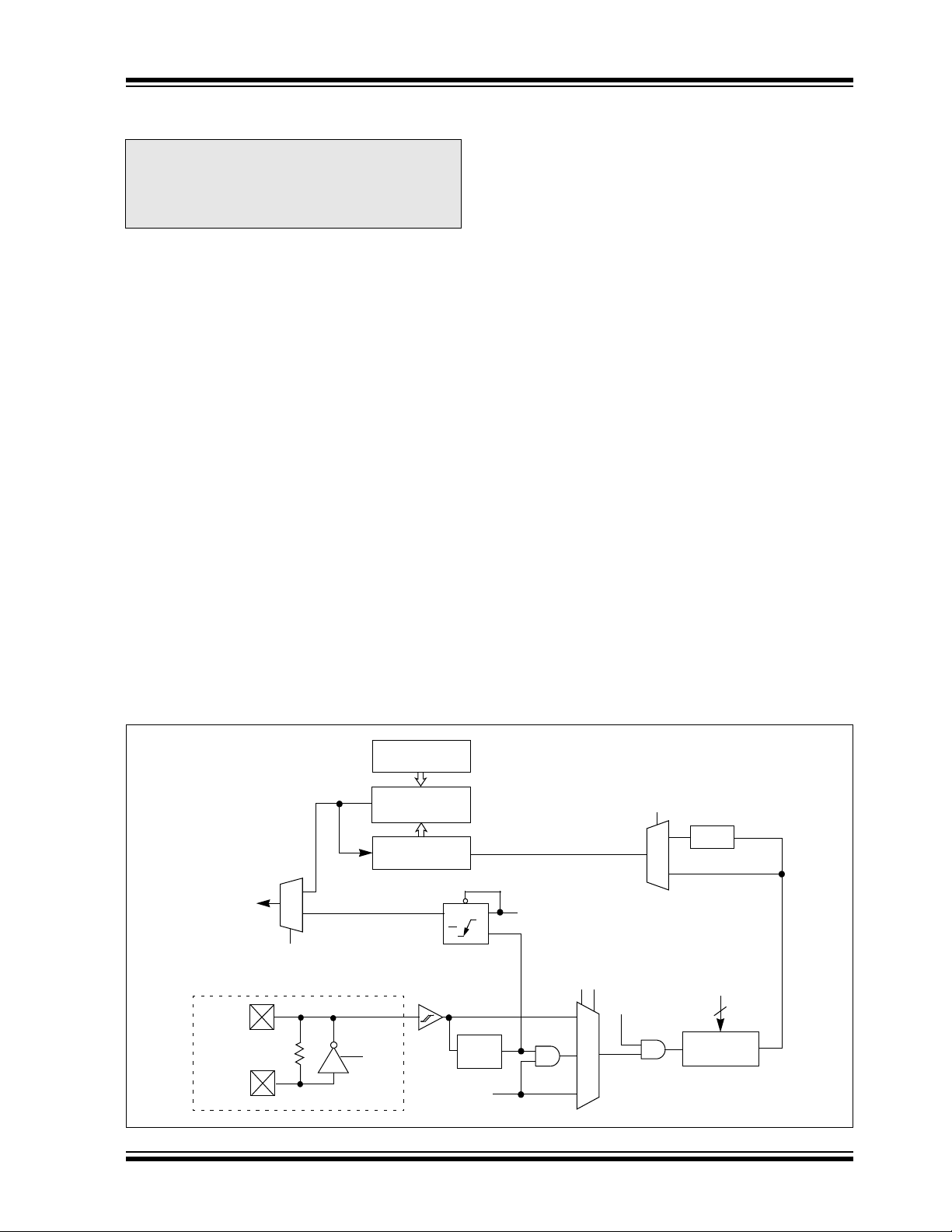
dsPIC30F
9.0 TIMER1 MODULE
Note: This data sheet summarizes features of this group
of dsPIC30F devices and is not intended to be a complete
reference source. For more information on the CPU,
peripherals, register descriptions and general device
functionality, refer to the dsPIC30F Family Reference
Manual (DS70046).
This section describes the 16-bit General Purpose
(GP) Timer1 module and associated Operational
modes. Figure 9-1 depicts the simplified block diagram
of the 16-bit Timer1 module.
The following sections provide a detailed description
including setup and control registers, along with associated block diagrams for the Operational modes of the
timers.
The Timer1 module is a 16-bit timer which can serve as
the time counter for the real-time clock, or operate as a
free-running interval timer/counter. The 16-bit timer has
the following modes:
• 16-bit Timer
• 16-bit Synchronous Counter
• 16-bit Asynchronous Counter
Further, the following operational characteristics are
supported:
• Timer gate operation
• Selectable prescaler settings
• Timer operation during CPU Idle and Sleep
modes
• Interrupt on 16-bit Period register match or falling
edge of external gate signal
These Operating modes are determined by setting the
appropriate bit(s) in the 16-bit SFR, T1CON. Figure 9-1
presents a block diagram of the 16-bit timer module.
16-bit Timer Mode: In the 16-bit Timer mode, the timer
increments on every instruction cycle up to a match
value preloaded into the Period register PR1, then
resets to ‘0’ and continues to count.
When the CPU goes into the Idle mode, the timer will
stop incrementing unless the TSIDL (T1CON<13>)
bit = 0. If TSIDL = 1, the timer module logic will resume
the incrementing sequence upon termination of the
CPU Idle mode.
16-bit Synchronous Counter Mode: In the 16-bit
Synchronous Counter mode, the timer increments on
the rising edge of the applied external clock signal
which is synchronized with the internal phase clocks.
The timer counts up to a match value preloaded in PR1,
then resets to ‘0’ and continues.
When the CPU goes into the Idle mode, the timer will
stop incrementing unless the respective TSIDL bit = 0.
If TSIDL = 1, the timer module logic will resume the
incrementing sequence upon termination of the CPU
Idle mode.
16-bit Asynchronous Counter Mode: In the 16-bit
Asynchronous Counter mode, the timer increments on
every rising edge of the applied external clock signal.
The timer counts up to a match value preloaded in PR1,
then resets to ‘0’ and continues.
When the timer is configured for the Asynchronous
mode of operation and the CPU goes into the Idle
mode, the timer will stop incrementing if TSIDL = 1.
FIGURE 9-1: 16-BIT TIMER1 MODULE BLOCK DIAGRAM
T1IF
Event Flag
SOSCO/
T1CK
SOSCI
TGATE
Equal
Reset
0
1
LPOSCEN
PR1
Comparator x 16
TMR1
Q
Q
D
CK
Gate
Sync
T
CY
TGATE
1 x
0 1
0 0
TCS
TGATE
TON
TSYNC
1
0
Sync
TCKPS<1:0>
2
Prescaler
1, 8, 64, 256
2004 Microchip Technology Inc. Preliminary DS70083G-page 81
Page 84
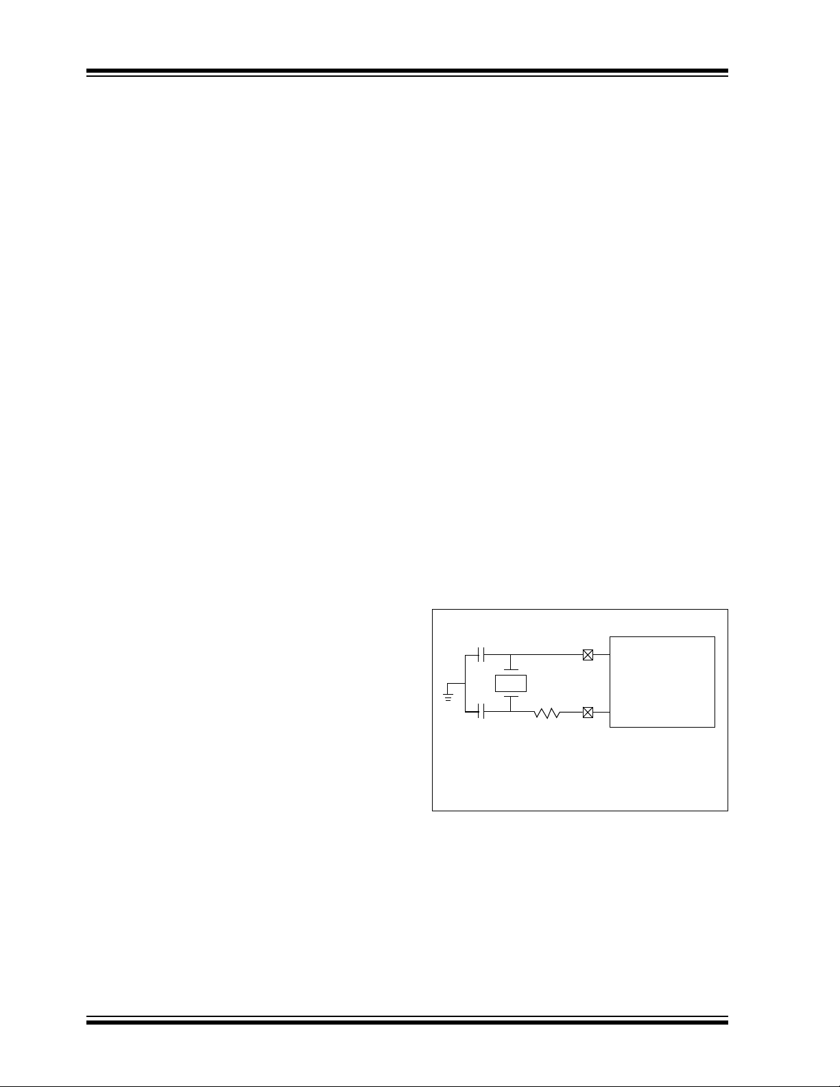
dsPIC30F
9.1 Timer Gate Operation
The 16-bit timer can be placed in the Gated Time Accumulation mode. This mode allows the internal T
increment the respective timer when the gate input signal (T1CK pin) is asserted high. Control bit TGATE
(T1CON<6>) must be set to enable this mode. The
timer must be enabled (TON = 1) and the timer clock
source set to internal (TCS = 0).
When the CPU goes into the Idle mode, the timer will
stop incrementing unless TSIDL = 0. If TSIDL = 1, the
timer will resume the incrementing sequence upon
termination of the CPU Idle mode.
CY to
9.2 Timer Prescaler
The input clock (FOSC/4 or external clock) to the 16-bit
Timer has a prescale option of 1:1, 1:8, 1:64 and 1:256,
selected by control bits TCKPS<1:0> (T1CON<5:4>).
The prescaler counter is cleared when any of the
following occurs:
• a write to the TMR1 register
• clearing of the TON bit (T1CON<15>)
• device Reset, such as POR and BOR
However, if the timer is disabled (TON = 0), then the
timer prescaler cannot be reset since the prescaler
clock is halted.
TMR1 is not cleared when T1CON is written. It is
cleared by writing to the TMR1 register.
9.3 Timer Operation During Sleep Mode
During CPU Sleep mode, the timer will operate if:
• The timer module is enabled (TON = 1) and
• The timer clock source is selected as external
(TCS = 1) and
• The TSYNC bit (T1CON<2>) is asserted to a logic
‘0’ which defines the external clock source as
asynchronous.
When all three conditions are true, the timer will continue to count up to the Period register and be reset to
0x0000.
When a match between the timer and the Period register occurs, an interrupt can be generated if the
respective timer interrupt enable bit is asserted.
9.4 Timer Interrupt
The 16-bit timer has the ability to generate an interrupt on
period match. When the timer count matches the Period
register, the T1IF bit is asserted and an interrupt will be
generated if enabled. The T1IF bit must be cleared in
software. The timer interrupt flag, T1IF, is located in the
IFS0 Control register in the interrupt controller.
When the Gated Time Accumulation mode is enabled,
an interrupt will also be generated on the falling edge of
the gate signal (at the end of the accumulation cycle).
Enabling an interrupt is accomplished via the respective timer interrupt enable bit, T1IE. The timer interrupt
enable bit is located in the IEC0 Control register in the
interrupt controller.
9.5 Real-Time Clock
Timer1, when operating in Real-Time Clock (RTC)
mode, provides time of day and event time-stamping
capabilities. Key operational features of the RTC are:
• Operation from 32 kHz LP oscillator
• 8-bit prescaler
•Low power
• Real-Time Clock interrupts
These Operating modes are determined by setting the
appropriate bit(s) in the T1CON Control register.
FIGURE 9-2: RECOMMENDED
COMPONENTS FOR
TIMER1 LP OSCILLATOR
RTC
C1
SOSCI
32.768 kHz
XTAL
C2
C1 = C2 = 18 pF; R = 100K
R
dsPIC30FXXXX
SOSCO
DS70083G-page 82 Preliminary 2004 Microchip Technology Inc.
Page 85

dsPIC30F
9.5.1 RTC OSCILLATOR OPERATION
When the TON = 1, TCS = 1 and TGATE = 0, the timer
increments on the rising edge of the 32 kHz LP oscillator output signal, up to the value specified in the Period
register and is then reset to ‘0’.
The TSYNC bit must be asserted to a logic ‘0’
(Asynchronous mode) for correct operation.
Enabling LPOSCEN (OSCCON<1>) will disable the
normal Timer and Counter modes and enable a timer
carry-out wake-up event.
When the CPU enters Sleep mode, the RTC will continue to operate provided the 32 kHz external crystal
oscillator is active and the control bits have not been
changed. The TSIDL bit should be cleared to ‘0’ in
order for RTC to continue operation in Idle mode.
9.5.2 RTC INTERRUPTS
When an interrupt event occurs, the respective interrupt
flag, T1IF, is asserted and an interrupt will be generated
if enabled. The T1IF bit must be cleared in software. The
respective Timer interrupt flag, T1IF, is located in the
IFS0 Status register in the interrupt controller.
Enabling an interrupt is accomplished via the respective timer interrupt enable bit, T1IE. The timer interrupt
enable bit is located in the IEC0 Control register in the
interrupt controller.
2004 Microchip Technology Inc. Preliminary DS70083G-page 83
Page 86
dsPIC30F
—TSIDL — — — — — — TGATE TCKPS1 TCKPS0 — TSYNC TCS — 0000 0000 0000 0000
SFR Name Addr. Bit 15 Bit 14 Bit 13 Bit 12 Bit 11 Bit 10 Bit 9 Bit 8 Bit 7 Bit 6 Bit 5 Bit 4 Bit 3 Bit 2 Bit 1 Bit 0 Reset State
TABLE 9-1: TIMER1 REGISTER MAP
DS70083G-page 84 Preliminary 2004 Microchip Technology Inc.
T1CON 0104 TON
TMR1 0100 Timer1 Register uuuu uuuu uuuu uuuu
PR1 0102 Period Register 1 1111 1111 1111 1111
Legend: u = uninitialized bit
Note: Refer to dsPIC30F Family Reference Manual (DS70046) for descriptions of register bit fields.
Page 87

dsPIC30F
10.0 TIMER2/3 MODULE
Note: This data sheet summarizes features of this group
of dsPIC30F devices and is not intended to be a complete
reference source. For more information on the CPU,
peripherals, register descriptions and general device
functionality, refer to the dsPIC30F Family Reference
Manual (DS70046).
This section describes the 32-bit General Purpose
(GP) Timer module (Timer2/3) and associated Operational modes. Figure 10-1 depicts the simplified block
diagram of the 32-bit Timer2/3 module. Figure 10-2
and Figure 10-3 show Timer2/3 configured as two
independent 16-bit timers, Timer2 and Timer3,
respectively.
The Timer2/3 module is a 32-bit timer (which can be
configured as two 16-bit timers) with selectable
Operating modes. These timers are utilized by other
peripheral modules, such as:
• Input Capture
• Output Compare/Simple PWM
The following sections provide a detailed description,
including setup and control registers, along with associated block diagrams for the Operational modes of the
timers.
The 32-bit timer has the following modes:
• Two independent 16-bit timers (Timer2 and
Timer3) with all 16-bit Operating modes (except
Asynchronous Counter mode)
• Single 32-bit timer operation
• Single 32-bit synchronous counter
Further, the following operational characteristics are
supported:
• ADC event trigger
• Timer gate operation
• Selectable prescaler settings
• Timer operation during Idle and Sleep modes
• Interrupt on a 32-bit period register match
These Operating modes are determined by setting the
appropriate bit(s) in the 16-bit T2CON and T3CON
SFRs.
For 32-bit timer/counter operation, Timer2 is the LS
Word and Timer3 is the MS Word of the 32-bit timer.
16-bit Timer Mode: In the 16-bit mode, Timer2 and
Timer3 can be configured as two independent 16-bit
timers. Each timer can be set up in either 16-bit Timer
mode or 16-bit Synchronous Counter mode. See
Section 9.0, Timer1 Module for details on these two
Operating modes.
The only functional difference between Timer2 and
Timer3 is that Timer2 provides synchronization of the
clock prescaler output. This is useful for high frequency
external clock inputs.
32-bit Timer Mode: In the 32-bit Timer mode, the timer
increments on every instruction cycle, up to a match
value preloaded into the combined 32-bit Period
register PR3/PR2, then resets to ‘0’ and continues to
count.
For synchronous 32-bit reads of the Timer2/Timer3
pair, reading the LS Word (TMR2 register) will cause
the MS word to be read and latched into a 16-bit
holding register, termed TMR3HLD.
For synchronous 32-bit writes, the holding register
(TMR3HLD) must first be written to. When followed by
a write to the TMR2 register, the contents of TMR3HLD
will be transferred and latched into the MSB of the
32-bit timer (TMR3).
32-bit Synchronous Counter Mode: In the 32-bit
Synchronous Counter mode, the timer increments on
the rising edge of the applied external clock signal
which is synchronized with the internal phase clocks.
The timer counts up to a match value preloaded in the
combined 32-bit period register PR3/PR2, then resets
to ‘0’ and continues.
When the timer is configured for the Synchronous
Counter mode of operation and the CPU goes into the
Idle mode, the timer will stop incrementing unless the
TSIDL (T2CON<13>) bit = 0. If TSIDL = 1, the timer
module logic will resume the incrementing sequence
upon termination of the CPU Idle mode.
Note: In some devices, one or more of the TxCK
pins may be absent. Therefore, for such
timers, the following modes should not be
used:
1. TCS = 1 (16-bit counter)
2. TCS = 0, TGATE = 1 (gated time
accumulation.
Note: For 32-bit timer operation, T3CON control
bits are ignored. Only T2CON control bits
are used for setup and control. Timer2
clock and gate inputs are utilized for the
32-bit timer module but an interrupt is generated with the Timer3 interrupt flag (T3IF)
and the interrupt is enabled with the
Timer3 interrupt enable bit (T3IE).
2004 Microchip Technology Inc. Preliminary DS70083G-page 85
Page 88
dsPIC30F
FIGURE 10-1: 32-BIT TIMER2/3 BLOCK DIAGRAM
Data Bus<15:0>
Write TMR2
Read TMR2
ADC Event Trigger
T3IF
Event Flag
TGATE
(T2CON<6>)
T2CK
TMR3HLD
16
16
Reset
Equal
0
1
TMR3 TMR2
Comparator x 32
PR3 PR2
16
Sync
LSB MSB
Q
D
TGATE (T2CON<6>)
CK
Q
TCS
1 x
TGATE
TON
TCKPS<1:0>
2
Gate
Sync
T
Note: Timer configuration bit T32 (T2CON<3>) must be set to ‘
bits are respective to the T2CON register.
CY
Prescaler
0 1
0 0
1, 8, 64, 256
1’ for a 32-bit timer/counter operation. All control
DS70083G-page 86 Preliminary 2004 Microchip Technology Inc.
Page 89
FIGURE 10-2: 16-BIT TIMER2 BLOCK DIAGRAM
dsPIC30F
T2IF
Event Flag
T2CK
0
1
TGATE
Equal
Reset
PR2
Comparator x 16
TMR2
Q
Q
D
CK
Gate
Sync
CY
T
FIGURE 10-3: 16-BIT TIMER3 BLOCK DIAGRAM
TGATE
TCS
1 x
0 1
0 0
TGATE
TON
Sync
TCKPS<1:0>
2
Prescaler
1, 8, 64, 256
ADC Event Trigger
T3IF
Event Flag
TGATE
T3CK
Equal
Reset
0
1
PR3
Comparator x 16
TMR3
Q
CK
Q
Sync
T
D
CY
TGATE
TCS
1 x
0 1
0 0
TGATE
TON
TCKPS<1:0>
2
Prescaler
1, 8, 64, 256
2004 Microchip Technology Inc. Preliminary DS70083G-page 87
Page 90

dsPIC30F
10.1 Timer Gate Operation
The 32-bit timer can be placed in the Gated Time Accumulation mode. This mode allows the internal T
increment the respective timer when the gate input signal (T2CK pin) is asserted high. Control bit TGATE
(T2CON<6>) must be set to enable this mode. When in
this mode, Timer2 is the originating clock source. The
TGATE setting is ignored for Timer3. The timer must be
enabled (TON = 1) and the timer clock source set to
internal (TCS = 0).
The falling edge of the external signal terminates the
count operation but does not reset the timer. The user
must reset the timer in order to start counting from zero.
CY to
10.2 ADC Event Trigger
When a match occurs between the 32-bit timer (TMR3/
TMR2) and the 32-bit combined period register (PR3/
PR2), or between the 16-bit timer (TMR3) and the 16bit period register (PR3), a special ADC trigger event
signal is generated by Timer3.
10.3 Timer Prescaler
The input clock (FOSC/4 or external clock) to the timer
has a prescale option of 1:1, 1:8, 1:64, and 1:256,
selected by control bits TCKPS<1:0> (T2CON<5:4>
and T3CON<5:4>). For the 32-bit timer operation, the
originating clock source is Timer2. The prescaler operation for Timer3 is not applicable in this mode. The
prescaler counter is cleared when any of the following
occurs:
• a write to the TMR2/TMR3 register
• clearing either of the TON (T2CON<15> or
T3CON<15>) bits to ‘0’
• device Reset, such as POR and BOR
However, if the timer is disabled (TON = 0), then the
Timer 2 prescaler cannot be reset since the prescaler
clock is halted.
TMR2/TMR3 is not cleared when T2CON/T3CON is
written.
10.4 Timer Operation During Sleep Mode
During CPU Sleep mode, the timer will not operate
because the internal clocks are disabled.
10.5 Timer Interrupt
The 32-bit timer module can generate an interrupt on
period match or on the falling edge of the external gate
signal. When the 32-bit timer count matches the
respective 32-bit period register, or the falling edge of
the external “gate” signal is detected, the T3IF bit
(IFS0<7>) is asserted and an interrupt will be generated if enabled. In this mode, the T3IF interrupt flag is
used as the source of the interrupt. The T3IF bit must
be cleared in software.
Enabling an interrupt is accomplished via the
respective timer interrupt enable bit, T3IE (IEC0<7>).
DS70083G-page 88 Preliminary 2004 Microchip Technology Inc.
Page 91
dsPIC30F
—TSIDL — — — — — — TGATE TCKPS1 TCKPS0 T32 —TCS — 0000 0000 0000 0000
—TSIDL — — — — — — TGATE TCKPS1 TCKPS0 — —TCS — 0000 0000 0000 0000
SFR Name Addr. Bit 15 Bit 14 Bit 13 Bit 12 Bit 11 Bit 10 Bit 9 Bit 8 Bit 7 Bit 6 Bit 5 Bit 4 Bit 3 Bit 2 Bit 1 Bit 0 Reset State
TMR2 0106 Timer2 Register uuuu uuuu uuuu uuuu
TMR3HLD 0108 Timer3 Holding Register (for 32-bit timer operations only) uuuu uuuu uuuu uuuu
TMR3 010A Timer3 Register uuuu uuuu uuuu uuuu
PR2 010C Period Register 2 1111 1111 1111 1111
PR3 010E Period Register 3 1111 1111 1111 1111
T2CON 0110 TON
T3CON 0112 TON
Legend: u = uninitialized bit
TABLE 10-1: TIMER2/3 REGISTER MAP
2004 Microchip Technology Inc. Preliminary DS70083G-page 89
Note: Refer to dsPIC30F Family Reference Manual (DS70046) for descriptions of register bit fields.
Page 92

dsPIC30F
NOTES:
DS70083G-page 90 Preliminary 2004 Microchip Technology Inc.
Page 93

dsPIC30F
11.0 TIMER4/5 MODULE
Note: This data sheet summarizes features of this group
of dsPIC30F devices and is not intended to be a complete
reference source. For more information on the CPU,
peripherals, register descriptions and general device
functionality, refer to the dsPIC30F Family Reference
Manual (DS70046).
This section describes the second 32-bit General Purpose (GP) Timer module (Timer4/5) and associated
Operational modes. Figure 11-1 depicts the simplified
block diagram of the 32-bit Timer4/5 module.
Figure 11-2 and Figure 11-3 show Timer4/5 configured
as two independent 16-bit timers, Timer4 and Timer5,
respectively.
The Timer4/5 module is similar in operation to the
Timer2/3 module. However, there are some differences
which are listed below:
• The Timer4/5 module does not support the ADC
event trigger feature
• Timer4/5 can not be utilized by other peripheral
modules, such as input capture and
output compare
FIGURE 11-1: 32-BIT TIMER4/5 BLOCK DIAGRAM
The Operating modes of the Timer4/5 module are
determined by setting the appropriate bit(s) in the
16-bit T4CON and T5CON SFRs.
For 32-bit timer/counter operation, Timer4 is the LS
Word and Timer5 is the MS Word of the 32-bit timer.
Note: For 32-bit timer operation, T5CON control
bits are ignored. Only T4CON control bits
are used for setup and control. Timer4
clock and gate inputs are utilized for the
32-bit timer module but an interrupt is generated with the Timer5 interrupt flag (T5IF)
and the interrupt is enabled with the
Timer5 interrupt enable bit (T5IE).
Note: In some devices, one or more of the TxCK
pins may be absent. Therefore, for such
timers, the following modes should not be
used:
1. TCS = 1 (16-bit counter)
2. TCS = 0, TGATE = 1 (gated time
accumulation)
T5IF
Event Flag
T4CK
Data Bus<15:0>
Write TMR4
Read TMR4
Reset
0
1
TGATE
(T4CON<6>)
Equal
TMR5HLD
16
16
TMR5
MSB
Comparator x 32
PR5 PR4
16
TMR4
LSB
Q
Q
D
TGATE (T4CON<6>)
CK
Gate
Sync
TCS
1 x
0
1
Sync
TGATE
TON
TCKPS<1:0>
2
Prescaler
1, 8, 64, 256
CY
T
Note: Timer configuration bit T32 (T4CON<3>) must be set to ‘1’ for a 32-bit timer/counter operation. All
control bits are respective to the T4CON register.
2004 Microchip Technology Inc. Preliminary DS70083G-page 91
0 0
Page 94

dsPIC30F
FIGURE 11-2: 16-BIT TIMER4 BLOCK DIAGRAM
T4IF
Event Flag
T4CK
0
1
TGATE
Equal
Reset
PR4
Comparator x 16
TMR4
Q
Q
D
CK
Gate
Sync
T
CY
FIGURE 11-3: 16-BIT TIMER5 BLOCK DIAGRAM
TGATE
TCS
1 x
0 1
0 0
TGATE
TON
Sync
TCKPS<1:0>
2
Prescaler
1, 8, 64, 256
ADC Event Trigger
T5IF
Event Flag
TGATE
T5CK
PR5
Equal
Reset
0
1
Comparator x 16
TMR5
Q
Q
D
CK
Sync
T
CY
TGATE
TCS
1 x
0 1
0 0
TGATE
TON
TCKPS<1:0>
2
Prescaler
1, 8, 64, 256
DS70083G-page 92 Preliminary 2004 Microchip Technology Inc.
Page 95

dsPIC30F
—TSIDL — — — — — — TGATE TCKPS1 TCKPS0 T45 —TCS— 0000 0000 0000 0000
—TSIDL — — — — — — TGATE TCKPS1 TCKPS0 — —TCS — 0000 0000 0000 0000
SFR Name Addr. Bit 15 Bit 14 Bit 13 Bit 12 Bit 11 Bit 10 Bit 9 Bit 8 Bit 7 Bit 6 Bit 5 Bit 4 Bit 3 Bit 2 Bit 1 Bit 0 Reset State
TMR4 0114 Timer 4 Register uuuu uuuu uuuu uuuu
TMR5HLD 0116 Timer 5 Holding Register (for 32-bit operations only) uuuu uuuu uuuu uuuu
TMR5 0118 Timer 5 Register uuuu uuuu uuuu uuuu
PR4 011A Period Register 4 1111 1111 1111 1111
PR5 011C Period Register 5 1111 1111 1111 1111
T4CON 011E TON
T5CON 0120 TON
Legend: u = uninitialized
TABLE 11-1: TIMER4/5 REGISTER MAP
2004 Microchip Technology Inc. Preliminary DS70083G-page 93
Note: Refer to dsPIC30F Family Reference Manual (DS70046) for descriptions of register bit fields.
Page 96

dsPIC30F
NOTES:
DS70083G-page 94 Preliminary 2004 Microchip Technology Inc.
Page 97
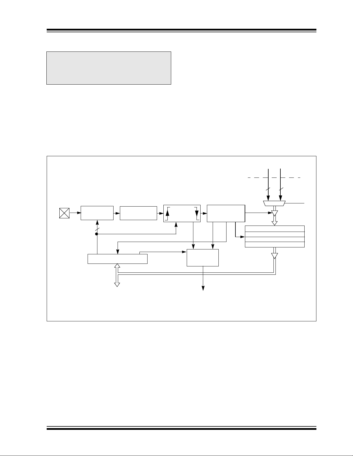
dsPIC30F
12.0 INPUT CAPTURE MODULE
The key operational features of the input capture
module are:
Note: This data sheet summarizes features of this group
of dsPIC30F devices and is not intended to be a complete
reference source. For more information on the CPU,
peripherals, register descriptions and general device
functionality, refer to the dsPIC30F Family Reference
Manual (DS70046).
This section describes the input capture module and
associated Operational modes. The features provided
by this module are useful in applications requiring fre-
• Simple Capture Event mode
• Timer2 and Timer3 mode selection
• Interrupt on input capture event
These Operating modes are determined by setting the
appropriate bits in the ICxCON register (where
x = 1,2,...,N). The dsPIC devices contain up to 8
capture channels (i.e., the maximum value of N is 8).
quency (period) and pulse measurement. Figure 12-1
depicts a block diagram of the input capture module.
Input capture is useful for such modes as:
• Frequency/Period/Pulse Measurements
• Additional Sources of External Interrupts
FIGURE 12-1: INPUT CAPTURE MODE BLOCK DIAGRAM
From GP Timer Module
ICx pin
Prescaler
1, 4, 16
3
Clock
Synchronizer
ICM<2:0>
Mode Select
ICBNE, ICOV
Edge
Detection
Logic
FIFO
R/W
Logic
T2_CNT
T3_CNT
16 16
10
ICxBUF
ICTMR
ICI<1:0>
ICxCON
Data Bus
Note: Where ‘x’ is shown, reference is made to the registers or bits associated to the respective input capture
channels 1 through N.
Interrupt
Logic
Set Flag
Set Flag
ICxIF
ICxIF
2004 Microchip Technology Inc. Preliminary DS70083G-page 95
Page 98

dsPIC30F
12.1 Simple Capture Event Mode
The simple capture events in the dsPIC30F product
family are:
• Capture every falling edge
• Capture every rising edge
• Capture every 4th rising edge
• Capture every 16th rising edge
• Capture every rising and falling edge
These simple Input Capture modes are configured by
setting the appropriate bits ICM<2:0> (ICxCON<2:0>).
12.1.1 CAPTURE PRESCALER
There are four input capture prescaler settings specified by bits ICM<2:0> (ICxCON<2:0>). Whenever the
capture channel is turned off, the prescaler counter will
be cleared. In addition, any Reset will clear the
prescaler counter.
12.1.2 CAPTURE BUFFER OPERATION
Each capture channel has an associated FIFO buffer
which is four 16-bit words deep. There are two status
flags which provide status on the FIFO buffer:
• ICBFNE - Input Capture Buffer Not Empty
• ICOV - Input Capture Overflow
The ICBFNE will be set on the first input capture event
and remain set until all capture events have been read
from the FIFO. As each word is read from the FIFO, the
remaining words are advanced by one position within
the buffer.
In the event that the FIFO is full with four capture
events and a fifth capture event occurs prior to a read
of the FIFO, an overflow condition will occur and the
ICOV bit will be set to a logic ‘1’. The fifth capture event
is lost and is not stored in the FIFO. No additional
events will be captured until all four events have been
read from the buffer.
If a FIFO read is performed after the last read and no
new capture event has been received, the read will
yield indeterminate results.
12.1.3 TIMER2 AND TIMER3 SELECTION
MODE
The input capture module consists of up to 8 input capture channels. Each channel can select between one of
two timers for the time base, Timer2 or Timer3.
Selection of the timer resource is accomplished
through SFR bit, ICTMR (ICxCON<7>). Timer3 is the
default timer resource available for the input capture
module.
12.1.4 HALL SENSOR MODE
When the input capture module is set for capture on
every edge, rising and falling, ICM<2:0> = 001, the following operations are performed by the input capture
logic:
• The input capture interrupt flag is set on every
edge, rising and falling.
• The interrupt on Capture mode setting bits,
ICI<1:0>, is ignored since every capture
generates an interrupt.
• A capture overflow condition is not generated in
this mode.
DS70083G-page 96 Preliminary 2004 Microchip Technology Inc.
Page 99

dsPIC30F
12.2 Input Capture Operation During Sleep and Idle Modes
An input capture event will generate a device wake-up
or interrupt, if enabled, if the device is in CPU Idle or
Sleep mode.
Independent of the timer being enabled, the input capture module will wake-up from the CPU Sleep or Idle
mode when a capture event occurs if ICM<2:0> = 111
and the interrupt enable bit is asserted. The same wakeup can generate an interrupt if the conditions for processing the interrupt have been satisfied. The wake-up
feature is useful as a method of adding extra external pin
interrupts.
12.2.1 INPUT CAPTURE IN CPU SLEEP
MODE
CPU Sleep mode allows input capture module operation with reduced functionality. In the CPU Sleep mode,
the ICI<1:0> bits are not applicable and the input capture module can only function as an external interrupt
source.
The capture module must be configured for interrupt
only on rising edge (ICM<2:0> = 111) in order for the
input capture module to be used while the device is in
Sleep mode. The prescale settings of 4:1 or 16:1 are
not applicable in this mode.
12.2.2 INPUT CAPTURE IN CPU IDLE
MODE
CPU Idle mode allows input capture module operation
with full functionality. In the CPU Idle mode, the Interrupt mode selected by the ICI<1:0> bits is applicable,
as well as the 4:1 and 16:1 capture prescale settings
which are defined by control bits ICM<2:0>. This mode
requires the selected timer to be enabled. Moreover,
the ICSIDL bit must be asserted to a logic ‘0’.
If the input capture module is defined as
ICM<2:0> = 111 in CPU Idle mode, the input capture
pin will serve only as an external interrupt pin.
12.3 Input Capture Interrupts
The input capture channels have the ability to generate
an interrupt based upon the selected number of capture events. The selection number is set by control bits
ICI<1:0> (ICxCON<6:5>).
Each channel provides an interrupt flag (ICxIF) bit. The
respective capture channel interrupt flag is located in
the corresponding IFSx Status register.
Enabling an interrupt is accomplished via the respective capture channel interrupt enable (ICxIE) bit. The
capture interrupt enable bit is located in the
corresponding IEC Control register.
2004 Microchip Technology Inc. Preliminary DS70083G-page 97
Page 100
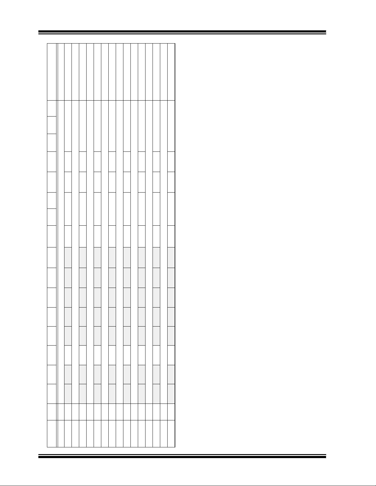
dsPIC30F
— —ICSIDL— — — — — ICTMR ICI<1:0> ICOV ICBNE ICM<2:0> 0000 0000 0000 0000
— —ICSIDL— — — — — ICTMR ICI<1:0> ICOV ICBNE ICM<2:0> 0000 0000 0000 0000
— —ICSIDL— — — — — ICTMR ICI<1:0> ICOV ICBNE ICM<2:0> 0000 0000 0000 0000
— —ICSIDL— — — — — ICTMR ICI<1:0> ICOV ICBNE ICM<2:0> 0000 0000 0000 0000
— —ICSIDL— — — — — ICTMR ICI<1:0> ICOV ICBNE ICM<2:0> 0000 0000 0000 0000
— —ICSIDL— — — — — ICTMR ICI<1:0> ICOV ICBNE ICM<2:0> 0000 0000 0000 0000
— —ICSIDL— — — — — ICTMR ICI<1:0> ICOV ICBNE ICM<2:0> 0000 0000 0000 0000
— —ICSIDL— — — — — ICTMR ICI<1:0> ICOV ICBNE ICM<2:0> 0000 0000 0000 0000
SFR Name Addr. Bit 15 Bit 14 Bit 13 Bit 12 Bit 11 Bit 10 Bit 9 Bit 8 Bit 7 Bit 6 Bit 5 B it 4 Bit 3 Bit 2 Bit 1 Bit 0 Reset State
IC1BUF 0140 Input 1 Capture Register uuuu uuuu uuuu uuuu
IC1CON 0142
IC2BUF 0144 Input 2 Capture Register uuuu uuuu uuuu uuuu
IC2CON 0146
IC3BUF 0148 Input 3 Capture Register uuuu uuuu uuuu uuuu
IC3CON 014A
IC4BUF 014C Input 4 Capture Register uuuu uuuu uuuu uuuu
IC4CON 014E
IC5BUF 0150 Input 5 Capture Register uuuu uuuu uuuu uuuu
IC5CON 0152
IC6BUF 0154 Input 6 Capture Register uuuu uuuu uuuu uuuu
IC6CON 0156
IC7BUF 0158 Input 7 Capture Register uuuu uuuu uuuu uuuu
IC7CON 015A
IC8BUF 015C Input 8 Capture Register uuuu uuuu uuuu uuuu
IC8CON 015E
Legend: u = uninitialized bit
TABLE 12-1: INPUT CAPTURE REGISTER MAP
Note: Refer to dsPIC30F Family Reference Manual (DS70046) for descriptions of register bit fields.
DS70083G-page 98 Preliminary 2004 Microchip Technology Inc.
 Loading...