

Page 1

dsPIC33CK Low-Voltage
Motor Control Board
User’s Guide
2020 Microchip Technology Inc. DS50002927A
Page 2

Note the following details of the code protection feature on Microchip devices:
• Microchip products meet the specification contained in their particular Microchip Data Sheet.
• Microchip believes that its family of products is one of the most secure families of its kind on the market today, when used in the
intended manner and under normal conditions.
• There are dishonest and possibly illegal methods used to breach the code protection feature. All of these methods, to our
knowledge, require using the Microchip products in a manner outside the operating specifications contained in Microchip’s Data
Sheets. Most likely, the person doing so is engaged in theft of intellectual property.
• Microchip is willing to work with the customer who is concerned about the integrity of their code.
• Neither Microchip nor any other semiconductor manufacturer can guarantee the security of their code. Code protection does not
mean that we are guaranteeing the product as “unbreakable.”
Code protection is constantly evolving. We at Microchip are committed to continuously improving the code protection features of our
products. Attempts to break Microchip’s code protection feature may be a violation of the Digital Millennium Copyright Act. If such acts
allow unauthorized access to your software or other copyrighted work, you may have a right to sue for relief under that Act.
Information contained in this publication regarding device
applications and the like is provided only for your convenience
and may be superseded by updates. It is your responsibility to
ensure that your application meets with your specifications.
MICROCHIP MAKES NO REPRESENTATIONS OR
WARRANTIES OF ANY KIND WHETHER EXPRESS OR
IMPLIED, WRITTEN OR ORAL, STATUTORY OR
OTHERWISE, RELATED TO THE INFORMATION,
INCLUDING BUT NOT LIMITED TO ITS CONDITION,
QUALITY, PERFORMANCE, MERCHANTABILITY OR
FITNESS FOR PURPOSE. Microchip disclaims all liability
arising from this information and its use. Use of Microchip
devices in life support and/or safety applications is entirely at
the buyer’s risk, and the buyer agrees to defend, indemnify and
hold harmless Microchip from any and all damages, claims,
suits, or expenses resulting from such use. No licenses are
conveyed, implicitly or otherwise, under any Microchip
intellectual property rights unless otherwise stated.
Trademarks
The Microchip name and logo, the Microchip logo, Adaptec,
AnyRate, AVR, AVR logo, AVR Freaks, BesTime, BitCloud, chipKIT,
chipKIT logo, CryptoMemory, CryptoRF, dsPIC, FlashFlex,
flexPWR, HELDO, IGLOO, JukeBlox, KeeLoq, Kleer, LANCheck,
LinkMD, maXStylus, maXTouch, MediaLB, megaAVR, Microsemi,
Microsemi logo, MOST, MOST logo, MPLAB, OptoLyzer,
PackeTime, PIC, picoPower, PICSTART, PIC32 logo, PolarFire,
Prochip Designer, QTouch, SAM-BA, SenGenuity, SpyNIC, SST,
SST Logo, SuperFlash, Symmetricom, SyncServer, Tachyon,
TempTrackr, TimeSource, tinyAVR, UNI/O, Vectron, and XMEGA
are registered trademarks of Microchip Technology Incorporated in
the U.S.A. and other countries.
APT, ClockWorks, The Embedded Control Solutions Company,
EtherSynch, FlashTec, Hyper Speed Control, HyperLight Load,
IntelliMOS, Libero, motorBench, mTouch, Powermite 3, Precision
Edge, ProASIC, ProASIC Plus, ProASIC Plus logo, Quiet-Wire,
SmartFusion, SyncWorld, Temux, TimeCesium, TimeHub,
TimePictra, TimeProvider, Vite, WinPath, and ZL are registered
trademarks of Microchip Technology Incorporated in the U.S.A.
Adjacent Key Suppression, AKS, Analog-for-the-Digital Age, Any
Capacitor, AnyIn, AnyOut, BlueSky, BodyCom, CodeGuard,
CryptoAuthentication, CryptoAutomotive, CryptoCompanion,
CryptoController, dsPICDEM, dsPICDEM.net, Dynamic Average
Matching, DAM, ECAN, EtherGREEN, In-Circuit Serial
Programming, ICSP, INICnet, Inter-Chip Connectivity, JitterBlocker,
KleerNet, KleerNet logo, memBrain, Mindi, MiWi, MPASM, MPF,
MPLAB Certified logo, MPLIB, MPLINK, MultiTRAK, NetDetach,
Omniscient Code Generation, PICDEM, PICDEM.net, PICkit,
PICtail, PowerSmart, PureSilicon, QMatrix, REAL ICE, Ripple
Blocker, SAM-ICE, Serial Quad I/O, SMART-I.S., SQI,
SuperSwitcher, SuperSwitcher II, Total Endurance, TSHARC,
USBCheck, VariSense, ViewSpan, WiperLock, Wireless DNA, and
ZENA are trademarks of Microchip Technology Incorporated in the
U.S.A. and other countries.
SQTP is a service mark of Microchip Technology Incorporated in
the U.S.A.
The Adaptec logo, Frequency on Demand, Silicon Storage
Technology, and Symmcom are registered trademarks of Microchip
Technology Inc. in other countries.
GestIC is a registered trademark of Microchip Technology Germany
II GmbH & Co. KG, a subsidiary of Microchip Technology Inc., in
other countries.
All other trademarks mentioned herein are property of their
respective companies.
© 2020, Microchip Technology Incorporated, All Rights Reserved.
For information regarding Microchip’s Quality Management Systems,
please visit www.microchip.com/quality.
ISBN: 978-1-5224-5762-6
DS50002927A-page 2 2020 Microchip Technology Inc.
Page 3

dsPIC33CK LOW-VOLTAGE
MOTOR CONTROL BOARD
USER’S GUIDE
Table of Contents
Preface ........................................................................................................................... 5
Chapter 1. Introduction.................................................................................................. 9
1.1 Overview ........................................................................................................ 9
1.2 Features ....................................................................................................... 10
1.3 Block Diagram .............................................................................................. 11
Chapter 2. Board Interface Description ..................................................................... 13
2.1 Introduction ................................................................................................... 13
2.2 Board Connectors ........................................................................................ 13
2.3 User Interface Hardware .............................................................................. 19
2.4 Pin Functions of the dsPIC DSC .................................................................. 25
Chapter 3. Hardware Description ............................................................................... 29
3.1 Introduction ................................................................................................... 29
3.2 Hardware Sections ....................................................................................... 29
Appendix A. Schematics and Layout......................................................................... 43
A.1 Board Schematics and Layout ..................................................................... 43
Appendix B. Electrical Specifications........................................................................ 55
B.1 Introduction .................................................................................................. 55
Appendix C. Design Details ........................................................................................ 57
C.1 Introduction .................................................................................................. 57
C.2 Current Amplifier Circuits ............................................................................. 57
C.3 Auxiliary Power Supply ................................................................................ 61
Worldwide Sales and Service .................................................................................... 66
2020 Microchip Technology Inc. DS50002927A-page 3
Page 4

dsPIC33CK Low-Voltage Motor Control Board User’s Guide
NOTES:
DS50002927A-page 4 2020 Microchip Technology Inc.
Page 5

dsPIC33CK LOW-VOLTAGE
MOTOR CONTROL BOARD
USER’S GUIDE
Preface
NOTICE TO CUSTOMERS
All documentation becomes dated, and this manual is no exception. Microchip tools and
documentation are constantly evolving to meet customer needs, so some actual dialogs and/
or tool descriptions may differ from those in this document. Please refer to our website
(www.microchip.com) to obtain the latest documentation available.
Documents are identified with a “DS” number. This number is located on the bottom of each
page, in front of the page number. The numbering convention for the DS number is
“DSXXXXXXXXA”, where “XXXXXXXX” is the document number and “A” is the revision level
of the document.
For the most up-to-date information on development tools, see the MPLAB
Select the Help menu, and then Topics to open a list of available online help files.
®
IDE online help.
INTRODUCTION
This preface contains general information that will be useful to know before using the
dsPIC33CK Low-Voltage Motor Control Board. Topics discussed in this preface
include:
• Document Layout
• Conventions Used in this Guide
• Recommended Reading
• The Microchip Website
• Product Change Notification Service
• Customer Support
• Document Revision History
DOCUMENT LAYOUT
The user’s guide describes the dsPIC33CK Low-Voltage Motor Control Board. The
document is organized as follows:
• Chapter 1. “Introduction” – This chapter introduces the board and provides a
brief overview of its features.
• Chapter 2. “Board Interface Description” – This chapter provides information
about the board input and output interfaces.
• Chapter 3. “Hardware Description” – This chapter describes the hardware
sections of the board.
• Appendix A. “Schematics and Layout” – This appendix provides board
schematics and layout.
• Appendix B. “Electrical Specifications” – This appendix summarizes the
electrical specifications.
• Appendix C. “Design Details” – This appendix provides design calculations for
certain hardware sections.
2020 Microchip Technology Inc. DS50002927A-page 5
Page 6

dsPIC33CK Low-Voltage Motor Control Board User’s Guide
CONVENTIONS USED IN THIS GUIDE
This manual uses the following documentation conventions:
DOCUMENTATION CONVENTIONS
Description Represents Examples
Arial font:
Italic characters Referenced books MPLAB
Emphasized text ...is the only compiler...
Initial caps A window the Output window
A dialog the Settings dialog
A menu selection select Enable Programmer
Quotes A field name in a window or
dialog
Underlined, italic text with
right angle bracket
Bold characters A dialog button Click OK
N‘Rnnnn A number in verilog format,
Text in angle brackets < > A key on the keyboard Press <Enter>, <F1>
Courier New font:
Plain Courier New Sample source code #define START
Italic Courier New A variable argument file.o, where file can be
Square brackets [ ] Optional arguments mcc18 [options] file
Curly braces and pipe
character: { | }
Ellipses... Replaces repeated text var_name [,
A menu path File>Save
A tab Click the Power tab
where N is the total number of
digits, R is the radix and n is a
digit.
Filenames autoexec.bat
File paths c:\mcc18\h
Keywords _asm, _endasm, static
Command-line options -Opa+, -Opa-
Bit values 0, 1
Constants 0xFF, ‘A’
Choice of mutually exclusive
arguments; an OR selection
Represents code supplied by
user
“Save project before build”
4‘b0010, 2‘hF1
any valid filename
[options]
errorlevel {0|1}
var_name...]
void main (void)
{ ...
}
®
IDE User’s Guide
DS50002927A-page 6 2020 Microchip Technology Inc.
Page 7

RECOMMENDED READING
This user’s guide describes how to use the dsPIC33CK Low-Voltage Motor Control
Board. The device-specific data sheets contain additional information on programming the
specific microcontroller or Digital Signal Controller (DSC) devices. Other useful
documents are listed below. The following Microchip documents are available and
recommended as supplemental reference resources:
dsPIC33CK256MP508 Family Data Sheet (DS70005349)
This document provides device-specific information for the dsPIC33CK256MP508
16-bit Digital Signal Controller with High-Resolution PWM and CAN Flexible Data
(CAN FD).
MCP2200 Data Sheet (DS50002106)
This document provides device-specific information for the MCP2200 USB 2.0 to
UART Protocol Converter with GPIO.
MPLAB® X IDE User’s Guide (DS50002027)
This document describes how to set up the MPLAB X IDE software and use it to
create projects and program devices.
Preface
AN1299, Single-Shunt Three-Phase Current Reconstruction Algorithm for
Sensorless FOC of a PMSM (DS01299)
AN1160, Sensorless BLDC Control with Back-EMF Filtering Using a
Majority Function (DS01160)
AN1078, Sensorless Field Oriented Control of a PMSM (DS01078)
AN1292, Sensorless Field Oriented Control (FOC) for a Permanent
Magnet Synchronous Motor (PMSM) Using a PLL Estimator and Field
Weakening (FW) (DS01292)
AN1017, Sinusoidal Control of PMSM Motors with dsPIC30F DSC
(DS01017)
Readme Files
For the latest information on using other tools, read the tool-specific Readme files in
the Readme subdirectory of the MPLAB X IDE installation directory. The Readme files
contain updated information and known issues that may not be included in this
user’s guide.
For step-by-step instructions to set up and run a motor control application using the
dsPIC33CK Low-Voltage Motor Control Board, refer to the Readme file provided along
with the motor control application code.
dsPIC33 Family Reference Manuals
Specific Family Reference Manuals (FRMs) are available for each module, which
explains the operation of the dsPIC
modules. The specifics of each device family are discussed in their data sheet.
To obtain any of these documents, visit the Microchip website at: www.microchip.com.
2020 Microchip Technology Inc. DS50002927A-page 7
®
DSC MCU family architecture and peripheral
Page 8

dsPIC33CK Low-Voltage Motor Control Board User’s Guide
THE MICROCHIP WEBSITE
Microchip provides online support via our website at www.microchip.com. This website
is used as a means to make files and information easily available to customers.
Accessible by using your favorite Internet browser, the website contains the following
information:
• Product Support – Data sheets and errata, application notes and sample
programs, design resources, user’s guides and hardware support documents,
latest software releases and archived software
• General Technical Support – Frequently Asked Questions (FAQs), technical
support requests, online discussion groups, Microchip consultant program
member listing
• Business of Microchip – Product selector and ordering guides, latest Microchip
press releases, listing of seminars and events, listings of Microchip sales offices,
distributors and factory representatives
PRODUCT CHANGE NOTIFICATION SERVICE
Microchip’s customer notification service helps keep customers current on Microchip
products. Subscribers will receive e-mail notification whenever there are changes,
updates, revisions or errata related to a specified product family or development tool of
interest.
To register, access the Microchip website at www.microchip.com, click on Product
Change Notification and follow the registration instructions.
CUSTOMER SUPPORT
Users of Microchip products can receive assistance through several channels:
• Distributor or Representative
• Local Sales Office
• Field Application Engineer (FAE)
• Technical Support
Customers should contact their distributor, representative or FAE for support. Local
sales offices are also available to help customers. A listing of sales offices and locations is included in the back of this document.
Technical support is available through the website at: http://support.microchip.com.
DOCUMENT REVISION HISTORY
Revision A (March 2020)
This is the initial released version of this document.
DS50002927A-page 8 2020 Microchip Technology Inc.
Page 9

dsPIC33CK LOW-VOLTAGE
MOTOR CONTROL BOARD
Chapter 1. Introduction
1.1 OVERVIEW
The dsPIC33CK Low-Voltage Motor Control Board is targeted to drive a low-voltage,
three-phase Permanent Magnet Synchronous Motor (PMSM) or Brushless DC (BLDC)
motor using the dsPIC33CK256MP508. This dsPIC
single-core 16-bit DSC with enhanced on-chip peripherals, such as
High-Resolution PWM (HRPWM),12-bit high-speed ADC cores, analog comparators with
DAC, op amps, QEI, CAN-FD, SENT, UART, SPI, I
In some instances of the document text, the dsPIC33CK Low-Voltage Motor Control Board
is also referred to as the ‘Motor Control Board’ to enhance readability. The Motor Control
Board is shown in Figure 1-1.
FIGURE 1-1: dsPIC33CK LOW-VOLTAGE MOTOR CONTROL BOARD
®
DSC features a 100 MIPS,
2
C, DMA, timers, etc.
USER’S GUIDE
2020 Microchip Technology Inc. DS50002927A-page 9
Page 10

dsPIC33CK Low-Voltage Motor Control Board User’s Guide
1.2 FEATURES
Key features of the Motor Control Board are as follows:
• Three-Phase Motor Control Power Stage with the Following Electrical Specifications:
- Input DC voltage: 12V to 48V
- Nominal phase RMS current: 10A at +25°C ambient temperature
• Motor Phase Current Feedbacks to Implement Field-Oriented Control (FOC) of a
PMSM/BLDC Motor
• DC Bus Current Feedback for Overcurrent Protection and to Implement Single
Shunt Current Reconstruction Algorithm
• DC Bus Voltage Feedback for Overvoltage Protection
• Phase Voltage Feedbacks to Implement Sensorless Trapezoidal Control
• Hall Sensor Interface
• Quadrature Encoder Interface (QEI)
• On-Board Temperature Sensor for Monitoring the MOSFET Temperature
• Optional External Temperature Sensor (thermistor) Interface
• Debug Serial Interface (USB to UART)
• PICkit™ On-Board (PKOB4) for Programming and Debugging
• Two mikroBUS™ Sockets to Support Connectivity, Sensors and Communication
Interfaces by Plugging in mikroBUS Add-On Boards
• User Interface Elements:
- Two debug LEDs
- One potentiometer
- Three push buttons
- PWM indication LEDs
- Power-on status indication LED
• Auxiliary Power Supply to Power External Interfaces and On-Board Circuitry
DS50002927A-page 10 2020 Microchip Technology Inc.
Page 11

1.3 BLOCK DIAGRAM
`
Debug
Interface
Push Buttons
LEDs
Potentiometer
DC-DC
Converter
(MIC28511)
DC-DC
Converter
(MCP16301)
+3.3V Output
LDO
(MCP1826)
Motor Terminal
Input Terminal
12-48 VDC, 24A
Input Jack
PKOB V4
MCLR
Push Button
ICSP Header
MIC4605 x 3
Half-Bridge MOSFET Drivers
Current
Sensing
Temp Sensor
for Thermal
Protection
Current
Sensing
Shunt
Position
Feedbacks
Quadrature
Encoder
Interface
Hall Sensor
Interface
Reset
Control
I/O Control – Analog, Digital, Pull-up, Pull -Down, Remappable, Change Notification
Program/
HR PWM
SCCP
DAC/
Comparators
QEI
Timer1
ADC – 2 x Dedicated Core and Shared Core
Op Amps
Clock
CLC
PTG
Interrupt
Control
Temperature
_
Current Shunt Feedbacks
Op Amps for
Phase
Currents
Amplification
I
A_EXT,
I
B_EXT,
I
C_EXT
Op Amp for
Bus Current
Amplification
I
BUS_EXT
Voltages
Scaling
Circuit
g
_A
,
_B
,
_C
I
BUS_FILT_EXT
p
g
DC Voltage
Scaling
Circuit
BUS
mikroBUS Socket-B
mikroBUS™ Socket-A
IA,
IB,
I
BUS
The block diagram of the dsPIC33CK Low-Voltage Motor Control Board is shown in
Figure 1-2. For more information on electrical specifications, refer to
Appendix B. “Electrical Specifications”.
FIGURE 1-2: THE MOTOR CONTROL BOARD BLOCK DIAGRAM
Introduction
Quadrature Encoder
Feedbacks
Speed/
EXT
TEMP
External
Interface
Hall Sensor Feedbacks
Three-Phase Inverter Bridge
J14
Connector
dsPIC33CK256MP508
V
V
V
es
Phase
Volta
MCP6024
Phase
PWMs
MCP651S
V
MOSFET Temperature
Three-Phase Inverter
Phase
Shunts
Bus
J2
Connector
MCP9700
CAN FD
PMP
WDT
SENT
DMT
UART
DMA
CRC
e
ut DC Volta
In
SPI
I2C
Other Interfaces
MCP2200
USB to UART Converter
+12V +5V
+12V Output
ICSP™
Debug
Auxiliary Power Supply
+5V Output
J1
Connector
12-24 VDC, 2.5A
User Interface
+3.3 VA
Program/
+3.3V
2020 Microchip Technology Inc. DS50002927A-page 11
Page 12

dsPIC33CK Low-Voltage Motor Control Board User’s Guide
NOTES:
DS50002927A-page 12 2020 Microchip Technology Inc.
Page 13

Chapter 2. Board Interface Description
2.1 INTRODUCTION
This chapter provides a more detailed description of the input and output interfaces of the
dsPIC33CK Low-Voltage Motor Control Board. This chapter covers the following topics:
• Board Connectors
• User Interface Hardware
• Pin Functions of the dsPIC DSC
2.2 BOARD CONNECTORS
This section summarizes the connectors on the Motor Control Board. The connectors
are intended for:
• Supplying input power to the Motor Control Board
• Delivering inverter outputs to the motor
• Interfacing motor position sensors, such as Hall sensors or the Quadrature
Encoder
• Enabling the user to program/debug the dsPIC33CK256MP508 device
• Interfacing the Click Boards™
• Establishing communication with the host PC
• Interfacing the external temperature sensor (thermistor)
The connectors on the Motor Control Board are shown in Figure 2-1 and summarized
in Ta b le 2 -1 .
dsPIC33CK LOW-VOLTAGE
MOTOR CONTROL BOARD
USER’S GUIDE
2020 Microchip Technology Inc. DS50002927A-page 13
Page 14

dsPIC33CK Low-Voltage Motor Control Board User’s Guide
J13
J10
J6
J3
J4
J11
J12
J9
J7
J8
J14
J16
J1
J2
FIGURE 2-1: CONNECTORS – dsPIC33CK LOW-VOLTAGE MOTOR CONTROL BOARD
TABLE 2-1: MOTOR CONTROL BOARD CONNECTORS
Connector
Designator
J1 3 Populated Input DC power supply jack
J2 2 Populated Input DC power supply – two-pin terminal connector (5 mm pitch,12-30 AWG wire insert)
J3 6 Not Populated UART interface connections
J4 2 Not Populated Erase jumper – used to switch PICkit™ On-Board (PKOB)
J6 5 Populated USB Micro-B connector for establishing the serial interface with the host PC
J7 6 Populated Hall sensor interface terminal connector (2.54 mm pitch, 20-30 AWG wire insert)
J8 6 Populated Quadrature Encoder Interface terminal connector (2.54 mm pitch,
J9 2 Not Populated External temperature sensor (thermistor) interface connector (2.5 mm pitch)
J10 6 Not Populated ICSP™ header – interfacing programming/debugging the dsPIC® DSC
J11 16 Populated mikroBUS™ socket for interfacing a Click Board™ with the Motor Control Board,
J12 16 Populated mikroBUS socket for interfacing a Click Board with the Motor Control Board, labeled
J13 5 Populated PICkit On-Board (PKOB) programmer/debugger interface connector (standard
J14 3 Populated Three-phase inverter output for connecting motor (5 mm pitch,
J16 2 Not Populated Jumper (2.54 mm pitch) which may be optionally used to connect the positive supply
No. of
Pins
Status Description
programmer/debugger to Boot Recovery mode through MPLAB
20-30 AWG wire insert)
labeled as ‘A’ on the board
as ‘B’ on the board
female USB Micro-B connector)
12-30 AWG wire insert)
DC
) input of connectors, J1 and J2; shorted by default on the board using PCB trace
(V
®
X IDE
DS50002927A-page 14 2020 Microchip Technology Inc.
Page 15

Board Interface Description
Auxiliary Power Supply
Three-Phase Inverter
VDC
NT1
Net Tie
J16
Jumper
Populated by Default
J2
J1
PGND
24A
2.5A
PGND
dsPIC33CK Low-Voltage Motor Control Board
Note 1: The Motor Control Board is designed to operate at a DC voltage range of 12V to 48V. When
powering the board through J1, limit the voltage to 24V Max. When the applied voltage is greater
than 24V, always use connector J2 to power the board.
2: When J1 and J2 are shorted through either J16 or NT1, always power the Motor Control Board
using only one connector, either J1 or J2.
2.2.1 Power Supply Connectors (J1, J2, J16)
The board is designed to operate in the DC voltage range of 12-48V. As shown in
Figure 2-2, the Motor Control Board can be powered through either coaxial plug J1 or
through terminal connector J2.
FIGURE 2-2: INPUT DC POWER SUPPLY CONNECTORS
(1,2)
If required, the power to the inverter can be disconnected by cutting the trace of the net
tie, NT1, and the rest of the circuitry can be powered through the supply connected to
the coaxial plug J1. The connection between the net tie can be bridged back by populating jumper J16, restoring the connection between J1 and J2, such that either input
connector, J1 or J2, can be used for powering the Motor Control Board. Connector J1
can carry current up to 2.5A and connector J2 can handle up to 24A. Ta bl e 2 -2 and
Ta bl e 2 -3 summarize the pin assignments of connectors, J1 and J2, respectively.
TABLE 2-2: PIN DESCRIPTION – CONNECTOR J1
Pin # Signal Name Pin Description
1VDC DC Input Supply Positive
2 PGND DC Input Supply Negative or PGND
3 PGND DC Input Supply Negative or PGND
Pin # Signal Name Pin Description
1 PGND DC Input Supply Negative or PGND
2VDC DC Input Supply Positive
TABLE 2-3: PIN DESCRIPTION – CONNECTOR J2
2020 Microchip Technology Inc. DS50002927A-page 15
Page 16

dsPIC33CK Low-Voltage Motor Control Board User’s Guide
2.2.2 UART Interface Header (J3)
A 5-pin header, J3, is a UART interface provided to connect an external UART-USB
converter or for accessing UART signals by disabling the MCP2200 device (see U13
in Figure A-5). Ta bl e 2 -4 summarizes the pin functions of connector J3.
TABLE 2-4: PIN DESCRIPTION – CONNECTOR J3
Pin # Signal Name Pin Description
1 +3.3V +3.3V Supply
2 DEBUG_TX UART Transmit Pin of dsPIC® DSC
3 DEBUG_RX UART Receive Pin of dsPIC DSC
4 DGND Digital Ground
5 MCP2200_RST Setting this Pin Low (connecting to Ground) will
Disable the MCP2200 (U13)
2.2.3 USB Serial Interface (J6)
The Motor Control Board uses an on-board MCP2200 device (see U13 in Figure A-5)
as a bridge between the UART and USB (see Table 2-5) for providing the host PC
interface.
TABLE 2-5: PIN DESCRIPTION – CONNECTOR J6
Pin # Signal Name Pin Description
0 No Connection Body is Connected to Digital Ground
1 5V_USB USB +5 V
2 UART_USB_N USB Data-
3 UART_USB_P USB Data+
4 No Connection —
5 GND Digital Ground
DC
2.2.4 Hall Sensor Interface Connector (J7)
Hall sensors are used to detect the rotor position and speed of the motor. Connector
J7 can be used to interface the Hall sensor outputs with the Motor Control Board,
enabling sensor-based BLDC motor control applications. Table 2-6 shows the pin
descriptions of connector J7. The connector provides two supply outputs, +5V and
+3.3V, which can be used as input supplies of the Hall sensors based on the sensor
specification.
TABLE 2-6: PIN DESCRIPTION – CONNECTOR J7
Pin # Signal Name Pin Description
1 +5V +5V Supply to Hall Sensors
2 +3.3V +3.3V Supply to Hall Sensors
3 DGND Digital Ground
4 HA Hall Sensor A Feedback from the Motor
5 HB Hall Sensor B Feedback from the Motor
6 HC Hall Sensor C Feedback from the Motor
DS50002927A-page 16 2020 Microchip Technology Inc.
Page 17

Board Interface Description
2.2.5 Quadrature Encoder Interface Connector (J8)
Quadrature Encoders are used to detect the rotor position and speed of the motor.
Connector J8 can be used to interface the encoder outputs with the Motor Control
Board, enabling sensor-based BLDC/PMSM motor control applications. Ta b le 2 -7
shows the pin description of connector J8. The connector provides two supply outputs,
+5V and +3.3V, which can be used as input supplies to the Quadrature Encoder based
on the encoder specification.
TABLE 2-7: PIN DESCRIPTION – CONNECTOR J8
Pin # Signal Name Pin Description
1 +5V +5V Supply to Quadrature Encoder
2 +3.3V +3.3V Supply to Quadrature Encoder
3 DGND Digital Ground
4 QEA Quadrature Encoder Phase A Feedback of the Motor
5 QEB Quadrature Encoder Phase B Feedback of the Motor
6 INDX Quadrature Encoder INDEX Feedback of the Motor
2.2.6 External Temperature Sensor Interface Connector (J9)
The 2-pin connector (2.5 mm pitch) J9 can be used for interfacing a thermistor to the
board. This is not populated by default. When needed, populate the connector with
Part Number B2B-EH-A(LF)(SN) or similar.
2.2.7 ICSP™ Header for Programmer/Debugger Interface (J10)
The 6-pin header J10 can be used for connecting the programmer/debugger, for
example, PICkit™ 3, for programming and debugging the dsPIC33CK256MP508.
This is not populated by default. When needed, populate the connector with
Part Number 68016-106HLF or similar. The pin details are provided in Table 2-8.
TABLE 2-8: PIN DESCRIPTION – CONNECTOR J10
Pin # Signal Name Pin Description
1MCLR
2DVDD Digital Supply Voltage
3 DGND Digital Ground
4 PGD Device Programming Data Line (PGD)
5 PGC Device Programming Clock Line (PGC)
6 No Connection —
Device Master Clear (MCLR)
2020 Microchip Technology Inc. DS50002927A-page 17
Page 18

dsPIC33CK Low-Voltage Motor Control Board User’s Guide
2.2.8 mikroBUS™ Sockets for Interfacing a Click Board™ (J11, J12)
Two mikroBUS sockets are provided on the Motor Control Board which can be used to
expand the functionality by attaching an add-on board, called a ‘Click Board’. The
mikroBUS sockets, J11 and J12, are labeled as ‘A’ and ‘B’, respectively. The
Motor Control Board implements the mikroBUS socket pinouts, as specified in the
“mikroBUS™ Standard Specifications v2.0” (refer to www.mikroe.com/mikrobus).
The pinout consists of three groups of communication pins (SPI, UART and I
additional pins (PWM, interrupt, analog input, Reset and chip select) and two power
groups (+3.3V-GND and 5V-GND).
For pin mapping information between the dsPIC DSC and the mikroBUS sockets, refer
to the schematics in Section A.1 “Board Schematics and Layout” or
Section 2.4 “Pin Functions of the dsPIC DSC”.
2.2.9 USB Connector for PKOB Interface (J13)
This is a standard female USB Micro-B connector that provides USB communication
when interfacing with the PICkit On-Board (PKOB) programming/debugging tool. Pin
assignments for connector J13 are shown in Ta bl e 2 -9 .
TABLE 2-9: PIN DESCRIPTION – CONNECTOR J13
Pin # Signal Name Pin Description
2
C), six
0 No Connection Body is Connected to GND
1VBUS USB 5V
2 D_N USB Data-
3 D_P USB Data+
4 No Connection —
5 GND PKOB Ground (GND)
2.2.10 Inverter Output Connector (J14)
The Motor Control Board can drive a three-phase PMSM/BLDC motor. Motor control
inverter outputs are available on connector J14. Pin assignments for connector J14 are
shown in Ta b le 2 - 10 .
TABLE 2-10: PIN DESCRIPTION – CONNECTOR J14
Pin # Signal Name Pin Description
1 PHASE C Phase 3 Output of Inverter
2 PHASE B Phase 2 Output of Inverter
3 PHASE A Phase 1 Output of Inverter
DS50002927A-page 18 2020 Microchip Technology Inc.
Page 19

Board Interface Description
LD1
LD2
LD3
LD11
LD10
LD4
LD5
LD7
LD6
LD9
LD8
2.3 USER INTERFACE HARDWARE
This section describes the LEDs, push buttons, potentiometer and test points available
on the Motor Control Board.
2.3.1 LEDs
The LEDs provided on the Motor Control Board are shown in Figure 2-3 and
summarized in Tab le 2- 11.
FIGURE 2-3: LEDs – dsPIC33CK LOW-VOLTAGE MOTOR CONTROL BOARD
TABLE 2-11: LEDs
LED
Designator
LD1 Yellow USB receive LED activity output. Refer to the “MCP2200 Data Sheet” for more details.
LD2 Green USB transmit LED activity output. Refer to the “MCP2200 Data Sheet” for more details.
LD3 Red Power-on status indication, connected to auxiliary supply output: +3.3V.
LD4 Green Indicates PWM1H (PWM_AH), used for controlling top MOSFET of the inverter Half-Bridge A.
LD5 Green Indicates PWM1L (PWM_AL), used for controlling bottom MOSFET of the inverter Half-Bridge A.
LD6 Green Indicates PWM2H (PWM_BH), used for controlling top MOSFET of the inverter Half-Bridge B.
LD7 Green Indicates PWM2L (PWM_BL), used for controlling bottom MOSFET of the inverter Half-Bridge B.
LD8 Green Indicates PWM4H (PWM_CH), used for controlling top MOSFET of the inverter Half-Bridge C.
LD9 Green Indicates PWM4L (PWM_CL), used for controlling bottom MOSFET of the inverter Half-Bridge C.
LD10 Yellow User-defined LED provided for debugging purposes (LED1).
LD11 Yellow User-defined LED provided for debugging purposes (LED2).
2020 Microchip Technology Inc. DS50002927A-page 19
LED
Color
LED Indication
Page 20

dsPIC33CK Low-Voltage Motor Control Board User’s Guide
SW1 SW2 SW3
SW4
MCLR
2.3.2 Push Buttons
The push buttons provided on the Motor Control Board are shown in Figure 2-4 and
summarized in Tab le 2- 12.
The push buttons, SW1, SW2 and SW3, are provided to control motor operations; for
example, starting or stopping the motor. The functions of these push buttons are
defined by the motor control application firmware.
FIGURE 2-4: PUSH BUTTONS – dsPIC33CK LOW-VOLTAGE MOTOR CONTROL BOARD
TABLE 2-12: PUSH BUTTONS
SI #
1 SW1 Push button provided for general purpose (BUTTON1).
2 SW2 Push button provided for general purpose (BUTTON2).
3 SW3 Push button provided for general purpose (BUTTON3).
4 SW4 This push button is tied to the MCLR
DS50002927A-page 20 2020 Microchip Technology Inc.
Push Button
Designator
will reset the dsPIC
®
DSC.
LED Indication
pin of the dsPIC33CK256MP508. Pressing this button
Page 21

Board Interface Description
POT1
2.3.3 Potentiometer
The potentiometer on the Motor Control Board (shown in Figure 2-5) is connected to
one of the analog inputs of the device and can be used for setting the speed reference.
FIGURE 2-5: POTENTIOMETER – dsPIC33CK LOW-VOLTAGE MOTOR CONTROL BOARD
2020 Microchip Technology Inc. DS50002927A-page 21
Page 22

dsPIC33CK Low-Voltage Motor Control Board User’s Guide
DGND
+12V
+5V
PGND
VDC
PGND
+3.3 VA
+3.3V
DGND
IBUS_EXT
IBUS_FILT_EXT
AGND
VBUS
IBUS
TP12
TP11
VB
VA
VC
IB_EXT
IA_EXT
IA
TP14
AGND
AL
AH
BH
BL
CH
CL
DGND
TP21
HALL_A
HALL_B
HALL_C
QEI_A
QEI_B
QEI_INDEX
QEI_HOME
HOME
DGND
LED1
LED2
IC_EXT
VREF
TP13
IB
2.3.4 Test Points
There are several test points on the Motor Control Board to monitor various signals,
such as motor feedback voltages, motor currents, auxiliary supply outputs, etc. These
test points are marked in Figure 2-6 and summarized in Table 2-13.
FIGURE 2-6: TEST POINTS – dsPIC33CK LOW-VOLTAGE MOTOR CONTROL BOARD
DS50002927A-page 22 2020 Microchip Technology Inc.
Page 23

Board Interface Description
TABLE 2-13: BOARD TEST POINTS
Test Point # Signal Description
Power Supply Inputs and Outputs
TP1 VDC Input DC Power Supply
TP3 +12V +12V Supply – output of on-board MIC28511 device-based
buck converter
TP7 PGND Power Ground
TP22 PGND Power Ground
TP4 +5V +5V Supply – output of on-board MCP16301 device-based buck converter
TP5 +3.3V +3.3V Digital Supply – output of on-board +3.3V LDO (MCP1826)
TP8 DGND Digital Ground
TP18 DGND Digital Ground
TP19 DGND Digital Ground
TP6 +3.3VA +3.3V Analog Supply
TP9 AGND Analog Ground
TP20 AGND Analog Ground
Analog Signals
TP17 V
IA IA Internal Amplifier (dsPIC33CK256MP508 Op Amp 1) output of Phase A leg
IA_EXT IA_EXT External Amplifier (MCP6024 U5A) output of Phase A leg current feedback of
IB IB Internal Amplifier (dsPIC33CK256MP508 Op Amp 2) output of Phase B leg
IB_EXT IB_EXT External Amplifier (MCP6024 U5B) output of Phase A leg current feedback of
IC_EXT IC_EXT External Amplifier (MCP6024 U5C) output of Phase A leg current feedback of
BUS IBUS Internal Amplifier (dsPIC33CK256MP508 Op Amp 3) output of bus current
I
IBUS_EXT IBUS_EXT External Amplifier (U15 MCP651S) output of bus current feedback of inverter
IBUS_FILT_EXT IBUS_FILT_EXT Filtered Bus Current Feedback of Inverter, which is amplified by MCP651S
VA VA Phase A Voltage Feedback
VB VB Phase B Voltage Feedback
VC VC Phase C Voltage Feedback
BUS VBUS DC Bus Voltage Feedback
V
TP14 TEMP_LOCAL MOSFET Temperature – output of on-board temperature sensor, MCP9700 (U14)
TP21 TEMP_EXT Output of External Temperature Sensor interfaced through connector J9
REF +1.65V Voltage Reference to bias op amp outputs
current feedback of inverter
inverter
current feedback of inverter
inverter
inverter
feedback of inverter
(U15); this output is connected to the negative input of one of the internal
comparators of dsPIC33CK256MP508 (U9) for overcurrent protection
2020 Microchip Technology Inc. DS50002927A-page 23
Page 24

dsPIC33CK Low-Voltage Motor Control Board User’s Guide
TABLE 2-13: BOARD TEST POINTS (CONTINUED)
Test Point # Signal Description
PWM Outputs
J15-1 AL PWM1L Output from dsPIC® DSC, which controls bottom MOSFET of the
Inverter Half-Bridge A
J15-2 AH PWM1H Output from dsPIC
Half-Bridge A
J15-3 BL PWM2L Output from dsPIC DSC, which controls bottom MOSFET of the
Inverter Half-Bridge B
J15-4 BH PWM2H Output from dsPIC DSC, which controls top MOSFET of the Inverter
Half-Bridge B
J15-5 CL PWM4L Output from dsPIC DSC, which controls bottom MOSFET of the
Inverter Half-Bridge C
J15-6 CH PWM4L Output from dsPIC DSC, which controls top MOSFET of the Inverter
Half-Bridge C
Hall Sensor Feedbacks
HALL_A HALL_A Hall Sensor A Feedback connected to dsPIC DSC input
HALL_B HALL_B Hall Sensor B Feedback connected to dsPIC DSC input
HALL_C HALL_C Hall Sensor C Feedback connected to dsPIC DSC input
Quadrature Encoder Feedbacks
QEI_A QEI_A Quadrature Encoder A Feedback connected to dsPIC DSC input
QEI_B QEI_B Quadrature Encoder B Feedback connected to dsPIC DSC input
QEI_INDEX QEI_INDEX Quadrature Encoder INDEX Feedback connected to dsPIC DSC input
QEI_HOME QEI_HOME Quadrature Encoder HOME Feedback connected to dsPIC DSC input
HOME HOME This test point can be optionally used to interface the HOME signal feedback
with the Motor Control Board
LEDs and General Purpose I/Os
LED1 LED1 LED1 Output from dsPIC
LED2 LED2 LED2 Output from dsPIC DSC
TP11 TP11 Connected to the port pin RE4 of the dsPIC DSC; this test point can be
optionally used as a general purpose input or output
TP12 TP12 Connected to the port pin RE5 of the dsPIC DSC; this test point can be
optionally used as a general purpose input or output
TP13 TP13 Connected to the port pin RE15 of the dsPIC DSC; this test point can be
optionally used as a general purpose input or output
DSC, which controls top MOSFET of the Inverter
®
DSC
DS50002927A-page 24 2020 Microchip Technology Inc.
Page 25

2.4 PIN FUNCTIONS OF THE dsPIC DSC
The on-board dsPIC33CK256MP508 device (see U9 in Figure A-2) enables the control
of various features of the Motor Control Board through its peripherals and CPU
capability. Pin functions of the dsPIC DSC are grouped according to their functionality
and presented in Ta bl e 2- 14 .
Board Interface Description
TABLE 2-14: dsPIC
Signal
dsPIC DSC Configuration – Supply, Reset, Clock and Programming
+3.3V 12, 31, 51, 71 V
DGND 11, 32, 50, 70 V
+3 .3VA 25 AV
AGND 26 AV
OSCI 34 OSCI/CLKI/AN5/RP32/
OSCO 35 OSCO/CLKO/AN6/RP33/
MCLR
PGD 55 PGD3/RP37/SDA2/PMA14/
PGC 56 PGC3/RP38/SCL2/RB6
dsPIC DSC Internal Amplifier Connections for Current Amplification
SHUNT_IA_P 20 OA1IN+/AN9/PMA6/RA2 Operational
SHUNT_IA_N 18 OA1IN-/ANA1/RA1
IA 16 OA1OUT/AN0/CMP1A/
SHUNT_IB_P 45 PGC2/OA2IN+/RP36/RB4 Operational
SHUNT_IB_N 43 PGD2/OA2IN-/AN8/RP35/
IB 41 OA2OUT/AN1/AN7/ANA0/
SHUNT_IBUS_P 29 OA3IN+/AN14/CMP2B/
SHUNT_IBUS_N 28 OA3IN-/AN13/CMP1B/
I
BUS
dsPIC® DSC
9MCLR Reset Connects to a push button (SW4), ICSP™
23 OA3OUT/AN4/CMP3B/
®
DSC PIN FUNCTIONS
Pin #
dsPIC DSC Pin Function
DD
SS
DD
SS
PMD10/PMA10/RB0
PMA1/PMALH/PSA1/RB1
PMCS1/PSCS/RB5
IBIAS0/RA0
RB3
CMP1D/CMP2D/CMP3D/
RP34/SCL3/INT0/RB2
ISRC1/RP50/PMD13/
PMA13/RC2
ISRC0/RP49/PMA7/RC1
IBIAS3/RA4
dsPIC DSC
Peripheral
Supply +3.3V digital supply to dsPIC DSC
Oscillator with PLL Connects to crystal (X2) on the board
In-Circuit Serial
Programming™
(ICSP™) or
In-Circuit Debugger
Amplifier 1
(Op Amp #1) and
Dedicated ADC
Core #0
Amplifier 2
(Op Amp #2) and
Dedicated ADC
Core #1
Operational
Amplifier 3
(Op Amp #3) and
Shared ADC Core
Remarks
Digital ground
+3.3V analog supply to dsPIC DSC
Analog Ground
header (J10) and PKOB circuit
Connects to ICSP header (J10) and
PKOB programming/debugging tool
Differential current feedback from shunt
resistor Rsh1 connects to noninverting and
inverting inputs of Op Amp #1 through input
resistors
Op Amp #1 output, which is amplified Phase A
current. For the output to be available, configure and enable Op Amp #1, populate the
resistor R125 (0R) in the amplifier feedback
and remove R121 if populated
Differential current feedback from shunt
resistor Rsh2 connects to noninverting and
inverting inputs of Op Amp #2 through input
resistors
Op Amp #2 output, which is amplified Phase B
current. For the output to be available, configure and enable Op Amp #2, populate the
resistor R133 (0R) in the amplifier feedback
and remove R129 if populated
Differential current feedback from shunt
resistor Rsh4 connects to noninverting and
inverting inputs of Op Amp #3 through input
resistors
Op Amp #3 output, which is amplified bus
current. For the output to be available, configure and enable Op Amp #3, populate the
resistor R141 (0R) in the amplifier feedback
and remove R137 if populated
2020 Microchip Technology Inc. DS50002927A-page 25
Page 26

dsPIC33CK Low-Voltage Motor Control Board User’s Guide
TABLE 2-14: dsPIC® DSC PIN FUNCTIONS (CONTINUED)
Signal
Amplified Currents from External Amplifiers: U5 and U15
IA_EXT 16 OA1OUT/AN0/CMP1A/
IB_EXT 41 OA2OUT/AN1/AN7/ANA0/
IBUS_EXT 23 OA3OUT/AN4/CMP3B/
Overcurrent Detection and Fault Output
IBUS_FILT_EXT 21 DACOUT1/AN3/CMP1C/RA3 High-Speed Analog
Voltage Feedbacks
V_BUS 33 AN15/CMP2A/IBIAS2/RP51/
V_A 30 AN17/ANN1/IBIAS1/RP54/
V_B 19 AN23/RE3 Shared ADC Core Phase B voltage feedback
V_C 17 AN22/RE2 Shared ADC Core Phase C voltage feedback
Temperature Feedbacks and Potentiometer (POT #1 – Speed Reference)
TEMP_LOCAL 15 AN12/ANN0/RP48/RC0 Shared ADC Core MOSFET die temperature sensed by
TEMP_EXT 58 TDO/AN2/CMP3A/RP39/
SPEED_
REFERENCE
Hall Sensor Feedbacks (Interfaced via Connector J7)
HALL_A 42 RE8 I/O Ports and
HALL_B 44 RE9
HALL_C 57 RE10
Quadrature Encoder Feedbacks (Interfaced via Connector J8)
QEI_A 5 RP60/PWM8H/PMD7/RC12 Remappable
QEI_B 6 RP61/PWM8L/PMA5/RC13
QEI_INDEX 7 RP62/PWM6H/PMA4/RC14
QEI_HOME 8 RP63/PWM6L/PMA3/RC15
Debug Interface (J6, J5 or PKOB)
DEBUG_RX 13 RP78/PCI21/RD14 Remappable
DEBUG_TX 14 ANN2/RP77/RD13
dsPIC® DSC
Pin #
61 PGC1/AN11/RP41/SDA1/RB9 Shared ADC Core Potentiometer (POT1) can be used for setting
dsPIC DSC Pin Function
IBIAS0/RA0
CMP1D/CMP2D/CMP3D/
RP34/SCL3/INT0/RB2
IBIAS3/RA4
PMD11/PMA11/RC3
PMD12/PMA12/RC6
SDA3/RB7
dsPIC DSC
Peripheral
Dedicated ADC
Core #0
Dedicated ADC
Core #1
Shared ADC Core Bus current amplified by the amplifier U15;
Comparator #1
(CMP #1) and
DAC #1
Shared ADC Core DC bus voltage feedback
Shared ADC Core Phase A voltage feedback
Shared ADC Core Feedback from external temperature sensor
Change
Notification (CN)
feature of I/O and
QEI
function of I/O and
UART
Phase Current A amplified by the amplifier
U5-A; when using this output, populate the
resistor R121 (0R), remove the resistor R125 if
populated and disable dsPIC DSC Operational
Amplifier #1
Phase Current B amplified by the amplifier
U5-B; when using this output, populate the
resistor R129 (0R), remove the resistor R133,
if populated and disable dsPIC DSC
Operational Amplifier #2
when using this output, populate the resistor
R137 (0R), remove the resistor R141, if populated and disable dsPIC DSC Operational
Amplifier #3
Amplified bus current is further filtered prior to
connecting to the positive input of the CMP #1
used for overcurrent detection. Overcurrent
threshold can be set through DAC. Comparator
output is internally available as Fault input of the
PWM Generators so that it can be used for
shutting down PWMs without CPU intervention.
MCP9700 (U14) can be used for thermal
protection
interfaced via connector J9
the speed reference in motor control application
Change Notification interrupt can be enabled
to identify the transitions of any of the Hall
sensor inputs
QEI module can be configured to read position
or speed information based on the encoder
signals as required by the motor control
application
These signals are connected to MCP2200
(U13), header J5 and PKOB; connect and
disconnect appropriate jumper resistors to
establish serial communication via any of
these channels
Remarks
DS50002927A-page 26 2020 Microchip Technology Inc.
Page 27

Board Interface Description
TABLE 2-14: dsPIC® DSC PIN FUNCTIONS (CONTINUED)
Signal
PWMs for Controlling Three-Phase Inverter (Q1 to Q6)
PWM_AH 1 RP46/PWM1H/PMD5/RB14 PWM Generator #1 Controls top MOSFET Q1 of the Inverter
PWM_AL 3 RP47/PWM1L/PMD6/RB15 Controls bottom MOSFET Q2 of the Inverter
PWM_BH 78 TDI/RP44/PWM2H/PMD3/
PWM_BL 80 RP45/PWM2L/PMD4/RB13 Controls bottom MOSFET Q4 of the Inverter
PWM_CH 73 RP65/PWM4H/RD1 PWM Generator #4 Controls top MOSFET Q5 of the Inverter
PWM_CL 74 RP64/PWM4L/PMD0/RD0 Controls bottom MOSFET Q6 of the Inverter
User Interface (LEDs, Push Buttons, General Purpose I/Os)
LED1 37 RE6 I/O Ports Connected to general purpose LED LD10
LED2 39 RE7 Connected to general purpose LED LD11
BUTTON1 59 RE11 Connected to push button SW1
BUTTON2 62 RE12 Connected to push button SW2
BUTTON3 64 RE13 Connected to push button SW3
TP11 22 RE4 Test point TP11 can be optionally used as a
TP12 24 RE5 Test point TP12 can be optionally used as a
TP13 79 RE15 Test point TP13 can be optionally used as a
Click Board™ Socket A Signals (J11)
CLICK_AN_A 4 AN21/RE1 Analog Channel or
CLICK_RST_A 77 RE14 GPIO
CLICK_CS_A 75 TMS/RP42/PWM3H/PMD1/
CLICK_SCK_A 27 RP76/RD12 Can be configured
CLICK_MISO_A 38 AN18/CMP3C/ISRC3/RP74/
CLICK_MOSI_A 36 AN19/CMP2C/RP75/PMA0/
CLICK_SDA_A 68 RP68/ASDA3/RD4 Alternate I
CLICK_SCL_A 69 RP67/ASCL3/RD3
CLICK_TX_A 40 AN16/ISRC2/RP55/PMD8/
CLICK_RX_A 52 RP71/PMD15/RD7
CLICK_INT_A 10 RP79/PCI22/PMA2/RD15 Can be configured
CLICK_PWM_A 76 TCK/RP43/PWM3L/PMD2/
dsPIC® DSC
Pin #
dsPIC DSC Pin Function
RB12
RB10
PMD9/PMA9/RD10
PMALL/PSA0/RD11
PMA8/RC7
RB11
dsPIC DSC
Peripheral
Phase A
Phase A
PWM Generator #2 Controls top MOSFET Q3 of the Inverter
GPIO
Remappable Pin or
PWM or GPIO
as SPI Input/
Output or Clock
through
Remappable
Feature
and Clock Pins of
2
I
C #3
Can be configured
as UART RX and
TX through
Remappable
Feature
as Interrupt Pin
through
Remappable
Feature
Can be configured
as SCCP Input or
Output or use PWM
Generator Output
2
C Data
Phase B
Phase B
Phase C
Phase C
general purpose input or output
general purpose input or output
general purpose input or output
Click Board socket is provided to extend the
feature by interfacing appropriated Click
Boards.
Pin feature requirement changes are based on
the Click Board inserted in the socket; the
signals are allocated as per the general
requirements.
Remarks
2020 Microchip Technology Inc. DS50002927A-page 27
Page 28

dsPIC33CK Low-Voltage Motor Control Board User’s Guide
TABLE 2-14: dsPIC® DSC PIN FUNCTIONS (CONTINUED)
Signal
Click Board™ Socket B Signals (J12)
CLICK_AN_B 2 AN20/RE0 Analog Input or
CLICK_RST_B 72 RP66/RD2 Remappable Pin or
CLICK_CS_B 48 RP73/PCI20/RD9 Remappable Pin or
CLICK_SCK_B 46 RP56/ASDA1/SCK2/RC8 Dedicated SPI #2
CLICK_MISO_B 49 RP72/SDO2/PCI19/RD8
CLICK_MOSI_B 47 RP57/ASCL1/SDI2/RC9
CLICK_SDA_B 63 RP52/PWM5H/ASDA2/RC4 Alternate I
CLICK_SCL_B 65 RP53/PWM5L/ASCL2/
CLICK_TX_B 54 RP69/PMA15/PMCS2/RD5 Can be configured
CLICK_RX_B 53 RP70/PMD14/RD6
CLICK_INT_B 67 RP59/PWM7L/RC11 Can be configured
CLICK_PWM_B 66 RP58/PWM7H/PMRD/
dsPIC® DSC
Pin #
dsPIC DSC Pin Function
PMWR/PMENB/PSWR/RC5
PMWR/PSRD/RC10
dsPIC DSC
Peripheral
GPIO
GPIO
PWM or GPIO
Pins
2
and Clock Pins of
2
I
C #2
as UART RX and
TX through
Remappable
Feature
as Interrupt Pin
through
Remappable
Feature
Can be configured
as SCCP Input or
Output or use as
PWM Generator
Output
C Data
Remarks
Click Board socket is provided to extend the
feature by interfacing appropriated Click
Boards.
Pin feature requirement changes based on the
Click Board inserted in the socket; the signals
are allocated as per the Click Board signal
generic requirements.
DS50002927A-page 28 2020 Microchip Technology Inc.
Page 29

Chapter 3. Hardware Description
3.1 INTRODUCTION
This chapter provides a detailed description of the hardware features of the
dsPIC33CK Low-Voltage Motor Control Board. The Motor Control Board is intended to
demonstrate the capability of the dsPIC33CK family of single core Digital Signal
Controllers (DSCs) for motor control applications.
The motor control inverter on the Motor Control Board is controlled by the highest pin
count variant dsPIC33CK256MP508 device from the dsPIC33CK family. The Motor
Control Board incorporates a Hall sensor/Quadrature Encoder Interface (QEI), and
sensing circuits to measure DC voltage, phase voltages, bus current and phase
currents, etc. In addition, a USB-UART interface, mikroBUS™ sockets and a PICkit™
On-Board (PKOB) programmer/debugger circuit are provided.
The motor control inverter can be operated by using an input voltage in the range of
12V to 48V and can deliver a continuous output phase current of 10A (RMS) in the
specified operating range. For more information on electrical specifications, see
Appendix B. “Electrical Specifications”.
dsPIC33CK LOW-VOLTAGE
MOTOR CONTROL BOARD
USER’S GUIDE
3.2 HARDWARE SECTIONS
This chapter covers the following hardware sections of the dsPIC33CK Low-Voltage
Motor Control Board:
• dsPIC33CK256MP508 and Auxiliary Circuits
• Power Supply
• Three-Phase Inverter Bridge
• Current Sensing Circuits
• Voltage Sensing Circuit
• Hall Sensor/Quadrature Encoder Interface
• External Temperature Sensor Interface
• User Interface
• Debug Serial UART Interface
• mikroBUS™ Sockets
• Programmer/Debugger Interface
Figure 3-1 and Ta b le 3 -1 describe the hardware sections of the Motor Control Board.
2020 Microchip Technology Inc. DS50002927A-page 29
Page 30

dsPIC33CK Low-Voltage Motor Control Board User’s Guide
1
11
9
8
10
4
4
1
8
4
4
3
6
7
2
5
FIGURE 3-1: HARDWARE SECTIONS
TABLE 3-1: HARDWARE SECTIONS
Section No. Hardware Sections
1 dsPIC33CK256MP508 and Auxiliary Circuits
2 Power Supply
3 Three-Phase Inverter Bridge
4 Current Sensing Circuits
5 Voltage Sensing Circuit
6 Hall Sensor/Quadrature Encoder Interface
7 External Temperature Sensor Interface
8 User Interface
9 Debug Serial UART Interface
10 mikroBUS™ Sockets
11 Programmer/Debugger Interface
DS50002927A-page 30 2020 Microchip Technology Inc.
Page 31

Hardware Description
3.2.1 dsPIC33CK256MP508 and Auxiliary Circuits
The dsPIC33CK Low-Voltage Motor Control Board features the dsPIC33CK256MP508
from Microchip’s dsPIC
®
DSC portfolio. dsPIC33C family devices implement a
100 MIPS high-performance dsPIC DSC core, and also integrate analog peripherals,
such as high-speed ADCs, op amps and analog comparators. The device also implements up to 16-channel, high-resolution Pulse-Width Modulators (PWMs) with built-in
Fault protection, triggering and synchronization features, which makes this dsPIC
device an ideal platform for the development of time-critical PMSM/BLDC motor control
applications.
The high-resolution PWM module in the dsPIC33C can generate, at specific instances,
multiple ADC triggers for measuring motor currents, phase voltages, inverter input voltage, total bus inverter current, etc. These feedbacks are required for implementing
motor control algorithms, such as sensor or sensorless Field-Oriented Control (FOC),
torque control, trapezoidal control, initial position detection, wind milling, flux
weakening and single-shunt current reconstruction. The PWM Control Input (PCI) of
the PWM module can be used for shutting down PWM outputs immediately when a
Fault is detected and synchronizing multiple PWM Generators (PGs) used for
controlling the three-phase inverter bridge.
The comparator module, along with the Digital-to-Analog Converter (DAC), can be
used for detecting overcurrent or overtemperature Faults to protect the inverter or
motor in case of malfunction. The dsPIC DSC has three operational amplifiers. These
can be configured by connecting an external input and feedback resistors for amplifying
currents sensed by shunt resistors.
The Change Notification (CN) feature of the I/O ports, along with the timer, can be used
for detection of Hall sensor state changes to obtain position and speed of the motor in
sensor-based BLDC motor control applications. Similarly, the Quadrature Encoder
Interface (QEI) in the dsPIC DSC can be configured to obtain the position/speed
information from the Quadrature Encoder feedbacks of the motor, which are required
for sensor-based Field-Oriented Control of PMSMs.
The dsPIC DSC also integrates several communication peripherals, such as CAN FD,
SENT, SPI, I
2
C and UART for communicating with the host PC, central controller or
master controller. Additionally, it features a Watchdog Timer, Deadman Timer, ECC
engine and BIST module required for safety-critical applications.
In the Motor Control Board, a provision is provided to mount an external crystal
oscillator to use its output as the dsPIC DSC clock input. Push button SW4 is tied to
the MCLR
pin of the device and is provided to reset the dsPIC DSC. One of the
program/debug pin pairs, PGC3/PGD3, of the dsPIC device is connected to the
programmer/debugger interfaces provided on the Motor Control Board, along with
MCLR
, to allow programming/debugging of the dsPIC33CK256MP508. Decoupling
capacitors are provided on all the power supply pins of the dsPIC DSC, including the
V
DD/GND and AVDD/AGND pairs.
2020 Microchip Technology Inc. DS50002927A-page 31
Page 32

dsPIC33CK Low-Voltage Motor Control Board User’s Guide
DC-DC
Converter
(MIC28511)
DC-DC
Converter
(MCP16301)
+3.3V Output
LDO
(MCP1826)
+5V
Input Terminal
Input Jack
MIC4605 x 3
Half-Bridge MOSFET Drivers
VDC
J16
Jumper
NT1
Net Tie
AGND
3.2.2 Power Supply
The Motor Control Board can be powered through coaxial plug J1 or terminal connector
J2. Connector J1 can carry current up to 2.5A and connector J2 can handle up to 24A.
The board is designed to operate in the DC voltage range of 12-48V. DC link capacitors
are placed in parallel with the input to minimize the effects of voltage variation, depending on the load, and to reduce ripple currents generated by the motor control inverter
during switching. The power supply block diagram is shown in Figure 3-2.
The input DC supply connects to the motor control inverter and auxiliary power supply.
The auxiliary power supply section consists of two DC-DC converters and an LDO voltage regulator. The MIC28511 synchronous buck converter generates +12V output,
which powers the three half-bridge gate drivers used for driving the MOSFETs of the
three-phase inverter. The MCP16301 buck converter generates a +5V output, which is
provided to power the speed/position sensors interfaced via connectors, J7 and J8, and
the Click Boards™ interfaced via the mikroBUS™ sockets, J11 and J12. The fixed 3.3V
LDO MCP1826 generates +3.3V, which powers all logical circuits, including the
dsPIC33CK256MP508, operational amplifiers, mikroBUS sockets, USB to UART
converter, user interface elements, temperature sensors, speed/position sensors and
programmer/debugger Interfaces.
FIGURE 3-2: POWER SUPPLY BLOCK DIAGRAM
Three-Phase Inverter
Three-Phase Inverter Bridge
J2
Connector
+12V
+3.3 VA
+3.3V
Auxiliary Power Supply
PGND
+12V Output
+5V Output
J1
Connector
DGND
The 3.3V digital and analog supply, and ground connections are logically separated
using jumper resistors. In the Motor Control Board design documents, the digital
supply, digital ground, analog supply and analog ground are labeled as +3.3V, DGND,
+3.3 VA and AGND, respectively.
When required, the power to the inverter can be separated by cutting the trace between
net tie NT1. Then, the rest of the circuitry can be powered through the coaxial plug J1
and only the three-phase inverter powered through connector J2. The connection
between the net tie can be bridged back by populating jumper J16, restoring
connections between J1 and J2.
For additional details, refer to C.3 “Auxiliary Power Supply”, Section 2.2.1 “Power
Supply Connectors (J1, J2, J16)” and Figure A-1.
DS50002927A-page 32 2020 Microchip Technology Inc.
Page 33

Hardware Description
+3.3 VA
R117
10k
R119
2.49k
U10
DNP
R120
7.5k
C74
DNP
C75
0.1 µF
AGND AGND AGND
R114
1k
C70
1000 pF
U5D
-D
+D
OUTD
MCP6024
R118
20R
V
REF
TP17
C72
0.1 µF
V
REF
13
12
14
1
32
3.2.3 Three-Phase Inverter Bridge
The three-phase motor power stage is implemented using six N-channel MOSFETs,
configured as three half-bridges. A resistor is connected across the gate and source of
each MOSFET to ensure a soft turn-off of the MOSFET when the gate signal is
disconnected. Low-ESR ceramic capacitors are provided across each half-bridge for
filtering high-frequency noise. The output of the three-phase inverter bridge is available
on connector J14.
Three half-bridge gate drivers (3 x MIC4605) are used for driving the low-side and
high-side MOSFETs of the motor control inverter. The high-side driver is powered by the
bootstrap circuit. The bootstrap circuit consists of an internal diode and an external
capacitor connected across to the gate driver HS and HB pins. The input pull-down resistors are internal to the gate driver. The gate drivers are powered by a +12V supply. Even
though the HS pin is rated for negative voltage, a diode resistor clamp is provided to
clamp the negative voltage on the HS pin to prevent excessive negative voltage from
damaging the driver. Depending upon the application and amount of negative voltage on
the switch node, a different resistor and diode can be selected. For more information,
refer to the “MIC4605 Data Sheet” (DS20005853) at: www.microchip.com.
3.2.4 Current Sensing Circuits
3.2.4.1 VOLTAGE REFERENCE CIRCUIT
The Reference Voltage (V
REF) is generated on the Motor Control Board; it is half the
analog supply voltage (+3.3 VA), that is, approximately +1.65V. This is used for providing a DC voltage shift on the op amp output, allowing measurement of positive and
negative current swings as a single supply amplifier is used for current amplification.
The reference circuit (see Figure 3-3) is built around one of the MCP6024 op amps
(labeled as ‘D’). The resistors, R117, R119 and R120, form the voltage divider circuit
and generate a voltage equal to half of the analog voltage (+3.3 VA). The op amp, U5D
(MCP6024-D), is used as a buffer. The resistors, R114, R118 and C70, form a compensation circuit to drive capacitive loads, where C70 acts as a high-frequency feedback
path and R114 is used as a feedback path for low-frequency signals. The reference
voltage is connected to the inputs of the current sensing amplifiers providing DC bias
to amplifier outputs.
FIGURE 3-3: VOLTAGE REFERENCE CIRCUIT
2020 Microchip Technology Inc. DS50002927A-page 33
Page 34

dsPIC33CK Low-Voltage Motor Control Board User’s Guide
3.2.4.2 CURRENT AMPLIFIERS
Field-Oriented Control (FOC) of the PMSM/BLDC motor requires the motor phase
current information for implementation. In the Motor Control Board, shunt resistors,
Rsh1, Rsh2 and Rsh3, are provided in each inverter leg to measure the amount of
current flowing through the motor phases. An additional shunt resistor, Rsh4, is
provided for sensing the total bus current as this information is necessary for overcurrent protection and current control of BLDC motors. The DC bus current information
can also be used for reconstruction of motor phase currents by appropriately sampling
currents during the PWM switching period, which is called a single-shunt reconstruction
algorithm.
Noninverting differential amplifier configuration is used for amplifying the voltage drop
across the shunt resistors proportional to the currents flowing through three-phase
Inverter Phases A, B and C, and bus current, respectively. The output voltage of the
amplifiers is shifted by Voltage Reference (V
current swings. The Common-mode and Differential-mode filters are added between
the input pins of all the amplifiers for noise filtering. It is also possible to add filters at
the output of the external amplifiers, U5-A, U5-B, U5-C
and U15.
The block diagram in Figure 3-4 illustrates the interconnections between the external
amplifiers and the dsPIC DSC analog peripherals, including internal amplifiers,
comparator, ADC, etc. The Motor Control Board enables phase and bus current amplification through external amplifiers, U5 and U15, and dsPIC DSC internal amplifiers,
Op Amp 1 (OA1), Op Amp 2 (OA2) and Op Amp 3 (OA3). The op amps, OA1, OA2 and
OA3, that are internal to dsPIC33CK256MP508, are used for Phase A, Phase B and
bus current amplification. Three out of four amplifiers (U5-A, U5-B and U5-C) in the
quad amplifier, MCP6024, are configured to amplify current flowing through Inverter
Phases A, B and C. Amplified Phase C current (IC_EXT) is connected directly to an
analog input of the dsPIC DSC. The selection between internal and external amplifier
outputs is done via resistor jumpers (see Table 3-2) for Phase A, Phase B and the bus
currents when they are used as current feedbacks.
The op amp, MCP651S (U15), is added for DC bus current amplification. This amplifier
is configured to sense bus current. The U15 amplifier output is further filtered
(IBUS_FILT_EXT) and is connected to the internal Comparator 1 positive input
(CMP1C). The Comparator 1 negative input is configured to use the internal DAC output to set the overcurrent threshold. The Comparator 1 output (CMP1) generates an
active-high output when overcurrent is detected. This comparator output is available to
the PWM Generators of the high-resolution PWM module as a Fault input. If the Fault
is enabled in the PWM Generators, and CMP1 is selected as an active-high Fault
source during an overcurrent Fault condition, the motor control PWMs will be disabled,
thus protecting the MOSFETs.
REF) +1.65V to allow positive and negative
DS50002927A-page 34 2020 Microchip Technology Inc.
Page 35

Hardware Description
TABLE 3-2: SELECTION BETWEEN EXTERNAL AND INTERNAL AMPLIFIER OUTPUTS
Jumper Resistor Settings
Current
Signal
Amplified Phase A
Currents
IA or IA_EXT
Amplified Phase B
Currents
IB or IB_EXT
Amplified Phase C
Currents
IC_EXT
Amplified Bus
Currents
IBUS or
IBUS_EXT
Populate Remove Populate Remove
R125 R121 R121 R125 In internal amplifier configuration,
configure and enable Op Amp 1 (OA1).
In external amplifier configuration,
ensure internal amplifier Op Amp 1
(OA1) is disabled.
R133 R129 R129 R133 In internal amplifier configuration,
configure and enable Op Amp 2 (OA2).
In external amplifier configuration,
ensure internal amplifier Op Amp 2
(OA2) is disabled.
Not Applicable Phase C current is amplified only by
external amplifier U5-C and its output
(IC_EXT) is connected directly to an
analog input of the dsPIC
R141 R137 R137 R141 In internal amplifier configuration,
configure and enable Op Amp 3 (OA3).
In external amplifier configuration,
ensure internal amplifier Op Amp 3
(OA3) is disabled.
RemarksInternal Amplifier Output External Amplifier Output
®
DSC.
The gain of the amplifier used for phase current and bus current sensing is set for
sensing 22A peak current by default. The gain of the amplifier can be changed, as
required by the application, by modifying the amplifier input and feedback resistors.
For more information, refer to C.2 “Current Amplifier Circuits”.
2020 Microchip Technology Inc. DS50002927A-page 35
Page 36

dsPIC33CK Low-Voltage Motor Control Board User’s Guide
PGND
Three-Phase Inverter Bridge
)
)
)
REF
REF
REF
REF
REF
REF
REF
DAC
REF
AGND
T
IB
0R
R125
IA
0R
R133
0R
R141
R137
I
BUS
Note 1: This is a representational diagram only; for detailed schematics, refer to Appendix A. “Schematics
and Layout”.
FIGURE 3-4: CURRENT SENSE CONFIGURATION
Phase A Current (-)
Phase A Current (+)
Phase B Current (-)
Phase B Current (+)
Phase C Current (-)
Phase C Current (+)
+1.65V (+3.3VA/2)
Phase A Current (+)
Phase A Current (-
V
(+1.65V)
V
(+1.65V)
V
(+1.65V)
V
(+1.65V)
Rsh1 (0.010ȍ)
Phase B Current (+)
Rsh1 (0.010ȍ)
Phase B Current (-
Bus Current (+)
Rsh1 (0.010ȍ)
Bus Current (-)
MCP6024
-
U5A
+
-
U5B
+
-
U5C
+
IA_EX
Phase A Current (-)
Phase A Current (+)
V
IB_EXT
Phase B Current (-)
Phase B Current (+)
V
IC_EXT
IBUS_EXT
Bus Current (-)
Bus Current (+)
V
-
U5D
+
(1)
VDC
Phase C Current (+)
Phase C Current (-)
(+1.65V)
(+1.65V)
(+1.65V)
Rsh1 (0.010ȍ
R121
DNP
R129
DNP
DNP
dsPIC33CK256MP508
-
OA1
+
-
OA2
+
ADC
-
OA3
+
HRPWM
PG1
PG2
PG4
Fault PCI I/P
Bus Current (-)
Bus Current (+)
V
(+1.65V)
DS50002927A-page 36 2020 Microchip Technology Inc.
MCP651S
-
U15
+
R108
IBUS_FILT_EXT
C66
-
CMP1
+
Page 37

3.2.5 Voltage Sensing Circuit
VBUS
301R
R83
V_BUS
DC Bus Voltage
VDC
3.3k
R87
0.1 μF
C52
V_A
V_B
PHASE_A
PHASE_B
V_C
PHASE_C
3.3k
R86
VB
301R
R82
3.3k
R84
VC
301R
R80
VA
301R
R81
3.3k
R85
1
2
3
BAS40-04
D6
1
2
3
BAS40-04
D5
1
2
3
BAS40-04
D4
1
2
3
BAS40-04
D7
AGND AGND AGND AGND
AGND
AGND
AGNDAGND
34k
R76
34k
R73
34k
R74
34k
R77
34k
R69
34k
R68
34k
R67
34k
R70
+3.3VA +3.3 VA
+3.3 VA
+3.3 VA
1000 pF
C51
1000 pF
C49
1000 pF
C50
A voltage sensing network is provided to scale down the DC supply voltage powering
the inverter to connect it to an analog channel of the dsPIC DSC for voltage measurement. The voltage divider network, formed by resistors, R69, R77 and R87, divides the
DC input voltage (V
DC input voltage (V_BUS) is connected to the analog input pin of the dsPIC DSC for
measurement.
FIGURE 3-5: VOLTAGE SENSING CIRCUIT
The Motor Control Board can also be to used to run BLDC motors with a trapezoidal
commutation scheme by monitoring back-EMF signals. For such an application, the
motor back-EMF is scaled down by voltage dividers before they are applied to the
analog channels of the dsPIC DSC. The filter capacitors are provided to filter the noise.
The voltage divider network divides phase voltages (PHASE_A, PHASE_B and
PHASE_C) at a voltage scaling ratio of 1:21.6 (see Figure 3-5). The scaled back-EMF
signals (V_A, V_B and V_C) are connected to analog input pins of the dsPIC DSC.
In case of any voltage transients, kickbacks or resistor failures, the clamping diodes are
provided at the scaled voltage outputs to ensure the voltages at the analog inputs do
not exceed the voltage limits of the dsPIC DSC inputs.
DC) at a voltage scaling ratio of 1:21.6 (see Figure 3-5). The scaled
Hardware Description
3.2.6 Hall Sensor/Quadrature Encoder Interface
The Motor Control Board can also be used to run PMSM/BLDC motor control
applications using the Hall sensor/Quadrature Encoder to determine rotor position and
speed. The connectors, J7and J8, are provided to interface Hall sensor feedback and
encoder feedback, respectively, with the Motor Control Board. The Hall sensor and
Quadrature Encoder Interface circuit supports either open-collector or push-pull
output sensors.
The Hall sensors and Quadrature Encoder can be powered by the +5V supply or +3.3V
supply available through the interface connector terminals. A capacitor is added to
each signal output to reduce the noise. The voltage divider can be configured to scale
down the sensor signal, from a +5V level to a +3.3V level, when push-pull output
sensors are powered by a +5V supply. For circuit details, refer to Figure A-6 in
Appendix A. “Schematics and Layout”.
The connector J7 and J8 pinouts are summarized in Section 2.2.4 “Hall Sensor
Interface Connector (J7)” and Section 2.2.5 “Quadrature Encoder Interface
Connector (J8)”.
2020 Microchip Technology Inc. DS50002927A-page 37
Page 38

dsPIC33CK Low-Voltage Motor Control Board User’s Guide
AGND
DNP
R98
AGND
TEMP_EXT
DNP
R93
DNP
C57
1
2
DNP
J9
+3.3 VA
TEMP_EXT
TP21
3.2.7 External Temperature Sensor Interface
The Motor Control Board provides an optional external temperature sensor interface
circuit. This circuit can be used to interface a thermistor for measuring motor winding
temperature, etc. As shown in Figure 3-6, the temperature sensor and resistor R98
form a +3.3V analog supply voltage divider, setting the voltage proportional to the
temperature at the analog input of the dsPIC DSC. To reduce the noise, temperature
feedback can be further filtered by the RC filter, R93 and C57. This circuit is not
populated by default. When used, populate the connector J9 with
Part Number B2B-EH-A(LF)(SN) or similar, and components, R98, R93 and C57,
appropriately.
FIGURE 3-6: EXTERNAL TEMPERATURE INTERFACE CIRCUIT
3.2.8 User Interface
The dsPIC33CK Low-Voltage Motor Control Board user interface has three
push buttons, along with a potentiometer and LEDs. The potentiometer (POT1) can be
used for setting the speed reference, LEDs (LD11, LD12) are for status indication and
the general purpose push buttons (SW1, SW2 and SW3) can be used to start and stop
the motor. The LEDs, LD4 to LD9, indicate the presence of PWM outputs, which are
used for controlling the motor control inverter. Additionally, test pads (TP11, TP12 and
TP13) are provided on the unused pins of the dsPIC33CK256MP508, which can be
configured and used as general purpose inputs or outputs based on application
requirements.
For details, refer to Section 2.3 “User Interface Hardware”.
DS50002927A-page 38 2020 Microchip Technology Inc.
Page 39

3.2.9 Debug Serial UART Interface
(U9)
(U13)
2
PKOB
Circuit
The board is equipped with a USB-UART interface based around the IC MCP2200. The
MCP2200 is a USB 2.0 to UART protocol converter with GPIO from the Microchip
‘Interfacing and Connectivity’ product portfolio. For a detailed description of these
products and the “MCP2200 Data Sheet” (DS20002228), visit the Microchip website:
www.microchip.com.
FIGURE 3-7: DEBUG SERIAL UART INTERFACE
Hardware Description
dsPIC33CK256MP508
DEBUG_TX
DEBUG_RX
R49 0R
R50 0R
The interconnections of debug serial UART Rx and Tx (labeled as DEBUG_RX and
DEBUG_TX) signals from the dsPIC33CK256MP508 are shown in Figure 3-7. These
signals are provided primarily to interface with MCP2200. To establish serial communication between the host PC and the Motor Control Board, connect a USB cable
between the host PC and Micro-B connector J6, which connects to the MCP2200
USB-UART converter. This USB-UART connection setup can support a baud rate of up
to 1 Mbps.
There is an additional header, J3, which is provided on the board to allow interfacing of
any other USB-UART serial converters. As shown in Figure 3-7, the UART Tx and Rx
signals between the dsPIC33CK256MP508 are connected to J3 (Pins #2 and #3).
When interfacing an external USB to UART converter through connector J3, disable
the on-board MCP2200 by holding its RST pin low. This can be done by connecting Pin
Number 5 of the J3 connector to DGND or removing resistor R153 (4.7k) and
populating R159 (4.7k).
The Rx and Tx signals of the dsPIC33CK256MP508 are connected to the PKOB circuit
by populating jumper resistors, R49 and R50, with 0 Ohms. This will allow the PICkit
On-Board (PKOB) programming/debugging tool to also be used as a debug serial
interface through the virtual COM port feature of the tool.
Collaterals, such as the USB driver, information related to driver installation and how to
access ports for operating systems (Linux
Microchip website (http://www.microchip.com/MCP2200). Under Windows OS, after
successful driver installation, the device will appear as the ‘COMx’ port object which
standard terminal programs can open to read and write data.
MCP2200
R157
0R
Rx
R158
0R
Tx
D+
D-
RST
+3.3V
R153
R159
DGND
®
, Mac® and Windows®) can be found on the
UART_USB_P
UART_USB_N
MCP2200_RST
DEBUG_TX
DEBUG_RX
J6
J3
5
3
2020 Microchip Technology Inc. DS50002927A-page 39
Page 40

dsPIC33CK Low-Voltage Motor Control Board User’s Guide
The MPLAB® X IDE hosts two plug-ins, which allow real-time diagnostics through a
serial USB-UART interface with external host PC. These are:
• X2C-Scope from the Linz Center of Mechatronics GmbH for use with the
X2C-Scope plug-in for MPLAB X IDE.
• RTDM from Microchip for use with the MPLAB DMCI plug-in.
3.2.10 mikroBUS™ Sockets
The Motor Control Board has two mikroBUS sockets, labeled ‘A’ and ‘B’. These
sockets are provided to attach mikroBUS add-on boards, called Click Boards™, to
expand the capability of the Motor Control Board by adding sensors, displays, storage
and communication interfaces. One hundred plus unique Click Boards are available
based on Microchip products (visit https://www.mikroe.com/brands/microchip) in categories, such as wireless connectivity (Wi-Fi, Bluetooth
position sensors, remote temperature, thermocouple, ECG, IrDA
LIN, Ethernet
®
, DALI™, EtherCAT), mixed signal (ADC, DAC), storage (EEPROM,
Flash, SRAM) and security, for example.
The mikroBUS socket comprises a pair of 1x8 female headers with an exclusive pin
configuration. The pinout consists of three communication interfaces, SPI, UART and
2
I
C, six additional pins for PWM, interrupt, analog input, Reset and chip select, and two
power groups, +3.3V and 5V. For available Click Boards, visit www.mikroe.com.
It is recommended that users verify that the connection requirement of the specific
Click Board is satisfied prior to interfacing. For pin mapping information between the
dsPIC DSC and the mikroBUS sockets, refer to the schematics in Section A.1 “Board
Schematics and Layout” or Section 2.4 “Pin Functions of the dsPIC DSC”. These
interfaces are not isolated from the input supply connected to the Motor Control Board.
®
, LoRa®), sensors (inductive
®
), interfaces (CAN,
DS50002927A-page 40 2020 Microchip Technology Inc.
Page 41

Hardware Description
3.2.11 Programmer/Debugger Interface
The board has a PICkit™ On-Board (PKOB) programming/debugging tool, which can
be used to program and debug the target device: dsPIC33CK256MP508 (U9). The
PKOB should automatically enumerate and be recognized by the MPLAB X IDE, v5.30
or later, when the dsPIC33CK Low-Voltage Motor Control Board is connected to the
host PC via the USB Micro-B connector, J13. No custom USB driver installation is
necessary as the PKOB relies on standard OS provided Human Interface Device (HID)
drivers, and therefore, the driver installation should be fully automatic. When plugged
in, the PKOB programmer/debugger tool can be selected from the MPLAB X IDE
project properties page by selecting the device under:
Hardware Tools>Microchip Kits>Starter Kits (PKOB)>Curiosity/Starter Kits(PKOB4)>
MPLAB PKoB 4,
as shown in Figure 3-8.
FIGURE 3-8: MPLAB PKoB 4 SELECTION IN MPLAB
®
X IDE
2020 Microchip Technology Inc. DS50002927A-page 41
Page 42

dsPIC33CK Low-Voltage Motor Control Board User’s Guide
Additionally, a 6-pin ICSP™ programming header, J10, is provided for connecting
the programmer/debugger (for example, PICkit™ 4 In-Circuit Debugger
Part Number: PG164140). For connector pin details, refer to Section 2.2.7 “ICSP™
Header for Programmer/Debugger Interface (J10)”.
The PKOB or ICSP programming header is not isolated from the input supply
connected to the Motor Control Board.
The debugger may need to be forced into Recovery Boot mode (reprogrammed) in rare
situations. In such situations, to use the Hardware Tool Emergency Boot Firmware
Recovery Utility, carefully follow the instructions found in MPLAB
main menu option Debug>Hardware Tool Emergency Boot Firmware Recovery
jumper connector J4 is provided in the PKOB Programming/Debugging Tool section of
the Motor Control Board to switch the PKOB to Recovery Boot mode. The location of
the J4 connector in the Motor Control Board is marked in Figure 2-1.
®
X IDE under the
. The
DS50002927A-page 42 2020 Microchip Technology Inc.
Page 43

Appendix A. Schematics and Layout
A.1 BOARD SCHEMATICS AND LAYOUT
This section provides schematics and PCB layout diagrams of the dsPIC33CK
Low-Voltage Motor Control Board. The Motor Control Board uses a four-layer FR4, 1.6
mm, Plated-Through-Hole (PTH) construction.
Ta bl e A - 1 summarizes the schematics of the Motor Control Board:
TABLE A-1: SCHEMATICS
Figure Index
Figure A-1 1 of 8 Input Power Supply Connections: +12V DC-DC Converter;
Figure A-2 2 of 8 dsPIC33CK256MP508 Interconnections: MCLR
Figure A-3 3 of 8 1.65V Voltage Reference Buffer: External Operational
Figure A-4 4 of 8 Motor Control Inverter: Gate Drivers; Three-Phase MOSFET
Figure A-5 5 of 8 Click Board Sockets (A, B); LED Indications; Push Buttons;
Figure A-6 6 of 8 Hall Sensor Interface Circuit; Quadrature Encoder Interface
Figure A-7 7 of 8 PKOB: Microcontroller; USB Port, etc.
Figure A-8 8 of 8 PKOB: Buffers
Schematics
Sheet No.
+5V DC-DC Converter; +3.3V LDO
ICSP™ Header; dsPIC
amplifying Bus Current and Phase Currents
Amplifiers for amplifying Bus Current and Phase Currents;
Potentiometer; DC Bus Voltage Sensing Circuit; Phase
Voltages Sensing Circuit; Temperature Sensing Circuits
Bridge
USB to UART Converter
Circuit
dsPIC33CK LOW-VOLTAGE
MOTOR CONTROL BOARD
USER’S GUIDE
Hardware Sections
®
DSC Operational Amplifiers for
Reset;
Ta bl e A - 2 summarizes the layout diagrams of the Motor Control Board:
TABLE A-2: PCB LAYERS
Figure Index Description
Figure A-9 Top Layer: Top Silk and Top Copper
Figure A-10 Mid Layer -1: Copper
Figure A-11 Mid Layer -2: Copper
Figure A-12 Bottom Layer: Bottom Silk and Bottom Copper
2020 Microchip Technology Inc. DS50002927A-page 43
Page 44

Designed with
Altium.com
PGND
MCP16301
BOOST
1
GND
2
V
FB
3
EN
4
SW
6
V
IN
5
U11
1N4148
D2
+5V
V
IN
1
GND
2
V
OUT
3
MCP1826S/3.3V
U12
+3.3 VA
2
3
1
POWER 2 mm
J1
1M
R16
V
DD
19
PV
DD
20
PV
IN
7
PV
IN
8
PV
IN
9
V
IN
17
FREQ
24
EN
16
DL (NC)
1
DH (NC)
3
SW
12
SW
21
(EPAD3) SW
27
LX
5
PV
IN
4
PVIN (EPAD1)
25
BST
6
I
LIM
18
FB
14
PGOOD
15
AGND
13
PGND
2
PGND
10
PGND
11
PGND
22
PGND
23
(EPAD2) PGND
26
MIC28511
U1
0.1uF
C2
0.1 μF
16V
C6
100k
R3
PGND
+12V
DNP
TP5
DNP
TP1
V
DC
DNP
TP4
+5V
DNP
TP6
0.1 μF
100V
C21
10 μF
25V
C23
10 μF
25V
C31
82R
R13
4.7R
R17
120 pF
100V
C33
MBRA140T3G
D3
52.3k
R14
10k
R18
1.21R
R2
2.2 μF
10V
C1
2.2 μF
10V
C3
100k
R8
100k
R7
DNP
R11
1.21R
R5
2.2 μF
100V
C15
22 μF
100V
C13
BAT46W
D1
10R
R1
DNP
C4
PGND
100 μH
L1
47 μF
35V
C7
2.2 μF
100V
C8
715R
R10
3300 pF
50V
C5
10 μF
16V
C100
10 μF
16V
C101
+12V
10 μF
16V
C104
10 μF
16V
C105
0R
0805
R15
0.1 μF
16V
C102
0.1 μF
16V
C103
0.1 μF
16V
C106
0.1 μF
16V
C22
0.1 μF
C39
PGND
PGND
0R
0805
R19
AGND
PGND
DGND
DGND
DNP
TP3
+12V
+3.3V
+3.3V
1k
R4
V
DC
PGND PGND
+3.3VA
DGND
AGND
Black TP
TP7
Black TP
TP8
Black TP
TP9
22 μH
L2
1
2
TERMINAL 1x2
J2
330 μF
63V
C10
330 μF
63V
C11
330 μF
63V
C12
330 μF
63V
C9
0.1 μF
C30
10k
R6
10k
R9
12
HDR-2.54 Male 1x2
J16
DGND
Black TP
TP18
DGND
Black TP
TP19
AGND
Black TP
TP20
Net Tie
0.5 mm
R12
Net Tie
5mm
NT1
PGND
Black TP
TP22
DS50002927A-page 44 2020 Microchip Technology Inc.
FIGURE A-1: SCHEMATICS PAGE 1 OF 8
dsPIC33CK Low-Voltage Motor Control Board User’s Guide
Page 45

2020 Microchip Technology Inc. DS50002927A-page 45
Internal Op Amp
OA2IN-
IB
OA2IN+
SHUNT_IB_N
SHUNT_IB_P
AGND
AGND
IB_EXT
VREF
OA3IN-
IBUS
OA3IN+
SHUNT_IBUS_N
SHUNT_IBUS_P
AGND
AGND
IBUS_EXT
VREF
OA1IN-
IA
OA1IN+
SHUNT_IA_N
VREF
+
-
+
-
+
-
0603
DNP
R137
0603
DNP
R129
IB
IBUS
OA2
OA3
OA1
The operational amplifiers, OA1, OA2 and OA3, are internal to dsPIC33CK256MP508
AGND
AGND
IA_EXT
0603
DNP
R121
SHUNT_IA_P
dsPIC33CK256MP508
MCLR
RP46/PWM1H/PMD5/RB14
1
AN20/RE0
2
RP47/PWM1L/PMD6/RB15
3
AN21/RE1
4
RP60/PWM8H/PMD7/RC12
5
RP61/PWM8L/PMA5/RC13
6
RP62/PWM6H/PMA4/RC14
7
RP63/PWM6L/PMA3/RC15
8
MCLR
9
RP79/PCI22/PMA2/RD15
10
Vඌඌ
11
Vൽൽ
12
RP78/PCI21/RD14
13
ANN2/RP77/RD13
14
AN12/ANN0/RP48/RC0
15
OA1OUT/AN0/CMP1A/IBIAS0/RA0
16
AN22/RE2
17
OA1IN-/ANA1/RA1
18
AN23/RE3
19
OA1IN+/AN9/PMA6/RA2
20
DACOUT1/AN3/CMP1C/RA3
21
RE4
22
OA3OUT/AN4/CMP3B/IBIAS3/RA4
23
RE5
24
AVൽൽ
25
AVඌඌ
26
RP76/RD12
27
OA3IN-/AN13/CMP1B/ISRC0/RP49/PMA7/RC1
28
OA3IN+/AN14/CMP2B/ISRC1/RP50/PMD13/PMA13/RC2
29
AN17/ANN1/IBIAS1/RP54/PMD12/PMA12/RC6
30
Vൽൽ
31
Vඌඌ
32
AN15/CMP2A/IBIAS2/RP51/PMD11/PMA11/RC3
33
OSCI/CLKI/AN5/RP32/PMD10/PMA10/RB0
34
OSCO/CLKO/AN6/RP33/PMA1/PMALH/PSA1/RB1
35
AN19/CMP2C/RP75/PMA0/PMALL/PSA0/RD11
36
RE6
37
AN18/CMP3C/ISRC3/RP74/PMD9/PMA9/RD10
38
RE7
39
AN16/ISRC2/RP55/PMD8/PMA8/RC7
40
OA2OUT/AN1/AN7/ANA0/CMP1D/CMP2D/CMP3D/RP34/SCL3/INT0/RB2
41
RE8
42
PGD2/OA2IN-/AN8/RP35/RB3
43
RE9
44
PGC2/OA2IN+/RP36/RB4
45
RP56/ASDA1/SCK2/RC8
46
RP57/ASCL1/SDI2/RC9
47
RP73/PCI20/RD9
48
RP72/SDO2/PCI19/RD8
49
Vඌඌ
50
Vൽൽ
51
RP71/PMD15/RD7
52
RP70/PMD14/RD6
53
RP69/PMA15/PMCS2/RD5
54
PGD3/RP37/SDA2/PMA14/PMCS1/PSCS/RB5
55
PGC3/RP38/SCL2/RB6
56
RE10
57
TDO/AN2/CMP3A/RP39/SDA3/RB7
58
RE11
59
PGD1/AN10/RP40/SCL1/RB8
60
PGC1/AN11/RP41/SDA1/RB9
61
RE12
62
RP52/PWM5H/ASDA2/RC4
63
RE13
64
RP53/PWM5L/ASCL2/PMWR/PMENB/PSWR/RC5
65
RP58/PWM7H/PMRD/PMWR/PSRD/RC10
66
RP59/PWM7L/RC11
67
RP68/ASDA3/RD4
68
RP67/ASCL3/RD3
69
Vඌඌ
70
Vൽൽ
71
RP66/RD2
72
RP65/PWM4H/RD1
73
RP64/PWM4L/PMD0/RD0
74
TMS/RP42/PWM3H/PMD1/RB10
75
TCK/RP43/PWM3L/PMD2/RB11
76
RE14
77
TDI/RP44/PWM2H/PMD3/RB12
78
RE15
79
RP45/PWM2L/PMD4/RB13
80
dsPIC33CK256MP508
U9
PWM_AL
OSCO
OSCI
OA2INOA2IN+
IB
OA3INOA3IN+
IBUS
OA1IN-
IA
OA1IN+
+3.3V
PWM_AH
PWM_BL
PWM_BH
PWM_CH
PWM_CL
CLICK_AN_B
CLICK_AN_A
QEI_A
QEI_B
QEI_INDEX
QEI_HOME
CLICK_INT_A
DEBUG_RX
DEBUG_TX
SPEED_REFERENCE
V_B
V_A
TEMP_EXT
CLICK_SCK_A
V_C
TEMP_LOCAL
CLICK_MOSI_A
LED1
CLICK_MISO_A
LED2 CLICK_TX_A
CLICK_SCK_B
CLICK_MOSI_B
CLICK_CS_B
CLICK_MISO_B
CLICK_RX_B
CLICK_TX_B
CLICK_RX_A
PGC
PGD
IBUS_FILT_EXT
BUTTON1
IC_EXT
V_BUS
BUTTON2
BUTTON3
CLICK_SDA_B
CLICK_SCL_B
CLICK_PWM_B
CLICK_INT_B
HALL_A
HALL_B
HALL_C
CLICK_RST_B
CLICK_RST_A
DNP
X2
OSCI OSCO
PIN 12
PIN 51
PIN 71
PIN 31
+3.3V
+3.3V
+3.3V
+3.3V
PIN25
PGC
PGD
+3.3V
4.7k
R142
+3.3V
14
23
PTS645SM43SMTR92 LFS
SW4
62R 1%
R144
1000 pF
50V
C96
470R 0.1%
R139
470R 0.1%
R145
62R 1%
R138
62R 1%
R134
1000 pF
50V
C87
470R 0.1%
R131
470R 0.1%
R135
62R 1%
R130
62R 1%
R126
1000 pF
50V
C80
470R 0.1%
R123
470R 0.1%
R127
62R 1%
R122
4.7 μF
10V
TANT-A
C77
0.1 μF
C78
0.1 μF
C81
0.1 μF
C85
0.1 μF
C89
0.1 μF
C92
0.1 μF
C99
0.1 μF
C97
DNP
C94
DNP
C95
IA
DNP
C76
DNP
C83
DNP
C84
DNP
C88
DNP
C91
DNP
C98
AGND
AGND
DGND
DGND
DGND
DGND
DGND
DGND
DGND DGND
DGND
+3.3 VA
+3.3 VA
0R
R125
0R
R133
0R
R141
10000 pF
C79
10000 pF
C82
10000 pF
C86
10000 pF
C90
10000 pF
C93
100R
R143
MCLR
MCLR
CLICK_CS_A
CLICK_PWM_A
CLICK_SCL_A
CLICK_SDA_A
DNP
TP11
DNP
TP12
DNP
TP13
4.02k
0.1%
R124
4.02k 0.1%
R132
4.02k
0.1%
R128
4.02k 0.1%
R136
4.02k 0.1%
R140
4.02k 0.1%
R146
1
2
3
4
5
6
ICSP™
MCLR
Vൽൽ
GND
PGD
PGC
AUX
DNP
J10
FIGURE A-2: SCHEMATICS PAGE 2 OF 8
Schematics and Layout
Page 46

DS50002927A-page 46 2020 Microchip Technology Inc.
External Op Amp
VREF
7.5k
R120
2.49k
R119
3
2
1
DNP
U10
0R
0603
R75
IA_EXT
IA_EXT
VREF
SHUNT_IA_P
SHUNT_IA_N
IB_EXT
SHUNT_IB_P
SHUNT_IB_N
IC_EXT
SHUNT_IC_P
SHUNT_IC_N
IBUS_EXT
SHUNT_IBUS_P
SHUNT_IBUS_N
IBUS_FILT_EXT
62R 1%
R71
62R 1%
R78
1000 pF
50V
C46
470R 0.1%
R72
470R 0.1%
R79
DNP
C48
DNP
C107
DNP
C47
-A
2
+A
3
OUTA
1
Vඌඌ
11
Vൽൽ
4
MCP6024
U5A
+B
5
-B
6
OUTB
7
OU
MCP6024
U5B
+C
10
-C
9
OUTC
8
C
C
OUTC
MCP6024
U5C
+D
12
-D
13
OUTD
14
D
D
OUTD
MCP6024
U5D
0R
0603
R94
IB_EXT
VREF
62R 1%
R90
62R 1%
R95
1000 pF
50V
C54
470R 0.1%
R91
470R 0.1%
R96
DNP
C59
DNP
C53
DNP
C56
0R
0603
R109
IC_EXT
VREF
62R 1%
R112
1000 pF
50V
C64
470R 0.1%
R106
470R 0.1%
R113
DNP
C69
62R 1%
R105
DNP
C62
DNP
C67
1k
R114
0R
0603
R107
VREF
62R 1%
R110
1000 pF
C63
470R 0.1%
R104
470R 0.1%
R111
DNP
C68
62R 1%
R103
DNP
C61
DNP
C65
+A
3
-A
4
OUTA
1
Vඌඌ
2
Vൽൽ
5
MCP651S
U15
0.1 μF
C73
0.1 μF
C71
0.1 μF
C72
1000 pF
C70
0.1 μF
C75
20R
R118
DNP
C74
Vඊඝඛ
301R
R83
V_BUS
DC Bus Voltage
VDC
3.3k
R87
0.1 μF
C52
V_A
V_B
Phase Voltage Feedbacks
PHASE_A
PHASE_B
V_C
PHASE_C
3.3k
R86
VB
301R
R82
3.3k
R84
VC
301R
R80
VA
301R
R81
3.3k
R85
AGND
DNP
R98
AGND
TEMP_EXT
Temperature Sensor Interface – External
DNP
R93
DNP
C57
GND
2
Vඈඎඍ
3
Vൽൽ
4
MCP9700
U14
TEMP_LOCAL
100R
R97
AGND
Temperature Sensor – MOSFET Thermal Protection
200R
R92
0.1 μF
C60
SPEED_REFERENCE
Speed Reference
0.1 μF
C58
1
2
3
BAS40-04
D6
1
2
3
BAS40-04
D5
1
2
3
BAS40-04
D4
1
2
3
BAS40-04
D7
1
2
DNP
J9
AGND
AGND
AGND
AGND
AGND
AGND
AGND
AGND
AGND
AGND
AGND AGND AGND
AGND
AGND
AGND
AGND
AGND AGND
AGNDAGND
AGND AGND AGND AGND
AGND
AGND
AGNDAGND
34k
R76
34k
R73
34k
R74
34k
R77
34k
R69
34k
R68
34k
R67
34k
R70
+3.3 VA
+3.3 VA
+3.3 VA
+3.3 VA
AGND
+3.3 VA
+3.3 VA
+3.3 VA
+3.3 VA
+3.3 VA
+3.3 VA
+3.3 VA
+3.3 VA
1 μF
C55
2
1
3
10k
POT1
IBUS_FILT_EXT
Voltage Reference
DC Bus Current Sensing Circuit
100R
R99
IBUS_EXT
1000 pF
C51
1000 pF
C49
1000 pF
C50
10k
R117
TEMP_EXT
TP21
TEMP_LOCAL
TP14
Vඋൾൿ
TP17
PGND
4.02k 0.1%
R66
4.02k 0.1%
R88
4.02k 0.1%
R89
4.02k 0.1%
R100
4.02k 0.1%
R102
4.02k 0.1%
R115
4.02k 0.1%
R101
4.02k 0.1%
R116
200R
R108
10000 pF
C66
FIGURE A-3: SCHEMATICS PAGE 3 OF 8
dsPIC33CK Low-Voltage Motor Control Board User’s Guide
-B
TB
-
-
Page 47

2020 Microchip Technology Inc. DS50002927A-page 47
HS_GATE_AHO_A
LS_GATE_ALO_A
HS_GATE_BHO_B
LS_GATE_BLO_B
HS_GATE_CHO_C
LS_GATE_CLO_C
SHUNT_IBUS_N
332k
R176
332k
R179
PHASE_A
SHUNT_IA_N
332k
R175
332k
R177
SHUNT_IB_P
332k
R174
332k
R178
SHUNT_IC_P
Vൽർ
PGND
SHUNT_IB_N
SHUNT_IC_N
SHUNT_IA_P
PGND PGND
HS_GATE_A
HS_GATE_B HS_GATE_C
LS_GATE_A
LS_GATE_B
LS_GATE_C
SHUNT_IBUS_P
PHASE_A
PHASE_B
PHASE_C
PHASE_B
PHASE_C
DNP
D10
DNP
D12
DNP
D8
DNP
D9
DNP
D11
DNP
D13
DNP
R198
HO_A
LO_A
1 μF
C138
PGND
PHASE_A
1 μF
C140
+12V
PGND
PWM_AH
PWM_AL
HO_B
LO_B
1 μF
C139
PGND
PHASE_B
PGND
1 μF
C141
+12V
PWM_BH
PWM_BL
HO_C
LO_C
1 μF
C136
PGND
PHASE_C
1 μF
C137
PGND
PWM_CH
PWM_CL
DNP
C132
2.2 μF
100V
C124
DNP
C125
DNP
C135
DNP
C130
DNP
C133
DNP
C131
DNP
C134
2.2 μF
100V
C126
DNP
C127
2.2 μF
100V
C128
DNP
C129
PGND PGND
PGND PGND
+12V
2.74R
R195
2.74R
R196
2.74R
R192
DNP
R197
DNP
R199
DNP
R200
DNP
R193
DNP
R194
DNP
R187
DNP
R191
DNP
R186
DNP
R190
DNP
R181
DNP
R183
VDC
HB
2
HO
3
HS
4
Vඌඌ
7
LI
6
LO8Vൽൽ
1
HI
5
MIC4605-1YM-TR
U16
HB
2
HO
3
HS
4
Vඌඌ
7
LI
6
LO8Vൽൽ
1
HI
5
MIC4605-1YM-TR
U17
HB
2
HO
3
HS
4
Vඌඌ
7
LI
6
LO8Vൽൽ
1
HI
5
MIC4605-1YM-TR
U18
0.01R
2512
±1%
Rsh2
0.01R
2512
±1%
Rsh3
0.01R
2512
±1%
Rsh4
4
1,2,3
5,6,7,8
SIR120DP
Q1
4
1,2,3
5,6,7,8
SIR120DP
Q2
4
1,2,3
5,6,7,8
SIR120DP
Q3
4
1,2,3
5,6,7,8
SIR120DP
Q4
4
1,2,3
5,6,7,8
SIR120DP
Q5
4
1,2,3
5,6,7,8
SIR120DP
Q6
1
2
3
TERMINAL 1x3
J14
0.01R
2512
±1%
Rsh1
PGNDPGND
PGNDPGND
PGNDPGND
VSSA210-E3/61T
D15
VSSA210-E3/61T
D16
VSSA210-E3/61T
D14
39R
0805
R185
39R
0805
R189
39R
0805
R188
39R
0805
R184
39R
0805
R182
39R
0805
R180
FIGURE A-4: SCHEMATICS PAGE 4 OF 8
Schematics and Layout
Page 48

DS50002927A-page 48 2020 Microchip Technology Inc.
1k
R161
1k
R162
1k
R163
1k
R164
PWM_AH
PWM_AL
LED1
LED2
1k
R165
1k
R166
PWM_BH
PWM_BL
1k
R167
1k
R168
PWM_CH
PWM_CL
BUTTON3
4.7k
R149
+3.3V
14
2
3
PTS645SM43SMTR92 LFS
SW3
BUTTON2
4.7k
R148
+3.3V
142
3
PTS645SM43SMTR92 LFS
SW2
BUTTON1
4.7k
R147
+3.3V
1
4
23
PTS645SM43SMTR92 LFS
SW1
GREEN
LD4
GREEN
LD5
GREEN
LD6
GREEN
LD7
GREEN
LD8
GREEN
LD9
RED
LD3
YELLOW
LD10
YELLOW
LD11
1k
R160
mikroBUS™ Interface A
+3.3V
CLICK_SCL_A
CLICK_SDA_A
CLICK_MISO_A
CLICK_MOSI_A
CLICK_SCK_A
CLICK_CS_A
CLICK_INT_A
CLICK_TX_A
CLICK_RX_A
CLICK_PWM_ACLICK_AN_A
CLICK_RST_A
AN
1
RST
2
CS
3
SCK
4
MISO
5
MOSI
6
+3.3V
7
GND
8
PWM
16
INT
15
RX
14
TX
13
SCL
12
SDA
11
+5V
10
GND
9
J11
Note:
PWM Indication LEDs
General Purpose LEDs
Power-on Status
DNP
R20
DNP
R21
+3.3V
+5V
I2C pull-ups are not populated, typically installed on mikroBUS daughter boards.
Diagnostics USB to UART Interface
ID
4
V
BUS
1
GND
5
D-
2
D+
3
0
USB Micro-B TH/SMT
J6
4.7k
R153
V
DD
1
OSC1
2
OSC2
3
RST
4
GP7/TxLED
5
GP6/RxLED
6
GP5
7
GP4
8
GP3
9
TX10RTS
11
RX
12
CTS
13
GP2
14
GP1
15
GP0
16
V
USB
17
D-
18
D+
19
V
SS
20
MCP2200
U13
2
3 1
12 MHz
X1
UART_USB_P
UART_USB_N
+3.3V+3.3V
5V_USB
UART_USB_N
UART_USB_P
1k
R154
1k
R156
GREEN
LD2
YELLOW
LD1
+3.3V +3.3V
MCP2200_RST
DNP
R159
0R
R158
DEBUG_RX 0R
R157
DEBUG_TX
5V_USB
12345
HDR-2.54 Male 1x5
DNP
J3
MCP2200_RST
DEBUG_RX
DEBUG_TX
+3.3V
mikroBUS™ Interface B
+3.3V CLICK_SCL_B
CLICK_SDA_B
CLICK_MISO_B
CLICK_MOSI_B
CLICK_SCK_B
CLICK_CS_B
CLICK_INT_B
CLICK_TX_B
CLICK_RX_B
CLICK_PWM_BCLICK_AN_B
CLICK_RST_B
AN
1
A
N
RST
2
CS
3
SCK
4
MISO
5
MOSI
6
+3.3V
7
GND
8
PWM
16
INT
15
RX
14
TX
13
SCL
12
SDA
11
+5V
10
GND
9
J12
Note:
DNP
R22
DNP
R169
+3.3V
+5V
I2C pull-ups are not populated, typically installed on mikroBUS daughter boards.
Push Buttons
+3.3V
0.1 μF
C108
0.1 μF
C116
0.1 μF
C117
DGND DGND
DGND DGND DGND
DGND
DGND DGND
DGND
DGND
DGND
DGND
DGND
DGND
DGND
DGND
DGND
DGND DGND
DGND DGND DGND DGND DGND DGND
DGND
DGND
100R
R150
100R
R151
100R
R152
LED2
TP16
LED1
TP15
PWM_CH
PWM_CL
PWM_BH
PWM_BL
PWM_AH
PWM_AL1
2
3
4
5
6
7
1
4
5
6
7
DNP
J15
DGND
0.1 μF
C118
0.1 μF
C119
0.1 μF
C120
0.1 μF
C121
0.1 μF
C122
0.1 μF
C123
0.1 μF
C142
FIGURE A-5: SCHEMATICS PAGE 5 OF 8
dsPIC33CK Low-Voltage Motor Control Board User’s Guide
3
Page 49

2020 Microchip Technology Inc. DS50002927A-page 49
+5V
HALL_A
HALL_C
HALL_A
HALL_B HALL_C
HAL L
100 pF
C109
100 pF
C110
100 pF
C111
HALL_B
4.7k
R170
4.7k
R171
4.7k
R172
Hall Sensor Interface
+5V
QEI_A
QEI_INDEX
QEI_A QEI_B QEI_INDEX QEI_HOME
QE I
QEI_B
QEI_HOME
+3.3V
+3.3V
Quadrature Encoder Interface
+3.3V
+3.3V
DGND DGND DGND DGND DGND DGND
DGND DGND DGND DGND DGND DGND DGND DGND
DGND
DGND
1
2
3
4
5
6
TERMINAL 1x6
J7
1
2
3
4
5
6
TERMINAL 1x6
J8
DNP
R202
DNP
R201
DNP
R52
100R
R173
100R
R204
100R
R203
2.2k
R62
2.2k
R63
2.2k
R64
2.2k
R65
1k
R58
1k
R59
1k
R60
1k
R61
DNP
R55
DNP
R57
DNP
R56
DNP
R54
10 pF
C112
10 pF
C113
10 pF
C143
10 pF
C144
Bumpon Hemisphere Black
PAD1 PAD2 PAD3 PAD4
SD103AW
D17
Fiducial
FD1
Fiducial
FD2
Fiducial
FD3
Fiducial
FD4
SD103AW
D18
SD103AW
D19
SD103AW
D20
SD103AW
D21
SD103AW
D22
SD103AW
D23
HOME
FIGURE A-6: SCHEMATICS PAGE 6 OF 8
Schematics and Layout
Page 50

DS50002927A-page 50 2020 Microchip Technology Inc.
D_P
D_N
ID
4
V
BUS
1
GND
5
D-
2
D+
3
0
USB MICRO-B FEMALE
J13
PICkit™ On-Board 4
PKOB USB Interface
3V3
DSC6011JI1A-012.0000
0.1 μF
25V
0603
C28
STB
1
GND2OUT
3
V
DD
4
12.00 MHz
X3
ATSAME70N21B-ANT
PA0/PWMC0_PWMH0/TIOA0/A17/BA1
72
PA1/PWMC0_PWML0/TIOB0/A18
70
PA2/PWMC0_PWMH1/DATRG
66
PA3/TWD0/LONCOL1/PCK2
64
PA4/TWCK0/TCLK0/UTXD1
55
PA5/WMC1_PWML3/ISI_D4/URXD1
52
PA7/XIN32
24
PA8/XOUT32
25
PA9/URXD0/ISI_D3/PWMC0_PWMFI0
54
PA10/UTXD0/PWMC0_PWMEXTRG0/RD
46
PA11/QCS/PWMC0_PWMH0/PWMC1_PWML0
44
PA12/QIO1/PWMC0_PWMH1/PWMC1_PWMH0
48
PA13/QIO0/PWMC0_PWMH2/PWMC1_PWML1
27
PA14/QSCK/PWMC0_PWMH3
34
PA15/D14/TIOA1/PWMC0_PWML3
33
PA16/D15/TIOB1/PWMC0_PWML2
30
PA17/QIO2/PCK1/PWMC0_PWMH3
16
PA18/PWMC1_PWMEXTRG1/PCK2/A14
15
PA19/PWMC0_PWML0/A15
14
PA20/PWMC0_PWML1/A16/BA0
13
PA21/RXD1/PCK1/PWMC1_PWMFI0
21
PA22/RK/PWMC0_PWMEXTRG1/NCS2
26
PA23/SCK1/PWMC0_PWMH0/A19
31
PA24/RTS1/PWMC0_PWMH1/A20
38
PA25/CTS1/PWMC0_PWMH2/A23
40
PA26/DCD1/TIOA2/MCDA2
42
PA27/DTR1/TIOB2/MCDA3
50
PA28/DSR1/TCLK1/MCCDA
79
PA30/PWMC0_PWML2/PWMC1_PWMEXTRG0
82
PA31/SPI0_NPCS1/PCK2/MCDA1
83
PB0/PWMC0_PWMH0/RXD0
12
PB1/PWMC0_PWMH1/GTSUCOMP/TXD0
11
PB2/CANTX0/CTS0
17
PB3/CANRX0/PCK2/RTS0
20
PB4/TDI/TWD1/PWMC0_PWMH2
74
PB5/TDO/TWCK1/PWMC0_PWML0
77
PB6/SWDIO/TMS
57
PB7/SWCLK/TCK
63
PB8/XOUT
98
PB9/XIN
99
PB12/ERASE/PWMC0_PWML1/GTSUCOMP
61
PB13/PWMC0_PWML2/PCK0/SCK0
100
PD0/GTXCK/PWMC1_PWML0/SPI1_NPCS1
1
PD1/GTXEN/PWMC1_PWMH0/SPI1_NPCS2
92
PD2/GTX0/PWMC1_PWML1/SPI1_NPCS3
91
PD3/GTX1/PWMC1_PWMH1/UTXD4
89
PD4/GRXDV/PWMC1_PWML2/TRACED0
88
PD5/GRX0/PWMC1_PWMH2/TRACED1
87
PD6/GRX1/PWMC1_PWML3/TRACED2
85
PD7/GRXER/PWMC1_PWMH3/TRACED3
84
PD8/GMDC/PWMC0_PWMFI1
80
PD9/GMDIO/PWMC0_PWMFI2/AFE1_ADTRG
78
PD10/PWMC0_PWML0/TD
71
PD11/GRX2/PWMC0_PWMH0/GTSUCOMP
69
PD12/GRX3/CANTX1/SPI0_NPCS2
65
PD13/GCOL/SDA10
62
PD14/GRXCK/SDCKE
59
PD15/GTX2/RXD2/NWR1/NBS1
75
PD16/GTX3/TXD2/RAS
56
PD17/GTXER/SCK2/CAS
53
PD18/NCS1/SDCS/RTS2/URXD4
49
PD19/NCS3/CTS2/UTXD4
47
PD20/PWMC0_PWMH0/SPI0_MISO/GTSUCOMP
45
PD21/PWMC0_PWMH1/SPI0_MOSI/TIOA11
43
PD22/PWMC0_PWMH2/SPI0_SPCK/TIOB11
41
PD24/PWMC0_PWML0/RF/TCLK11
37
PD25/PWMC0_PWML1/SPI0_NPCS1/URXD2
35
PD26/PWMC0_PWML2/TD/UTXD2
36
PD27/PWMC0_PWML3/SPI0_NPCS3/TWD2
32
PD28/URXD3/CANRX1/TWCK2
51
PD30/UTXD3
23
PD31/QIO3/UTXD3/PCK2
2
HSDP
95
HSDM
94
NRST
58
TST
60
JTAGSEL
73
V
REFP
9
V
REFN
6
VBG
97
U4A
UTIL_SDA
UTIL_SCL
ERASE
VPP_ON
VPP_GND
4.7k
0402
1%
R23
4.7k
0402
1%
R24
3V3
VDD_GND
PKOB4_SWDIO
PKOB4_SWCLK
PKOB4_TDO
DATA_EN
CLK_EN
PG_SYSTEM
((U)PDI_RXD1)
PDI_SCK1
((U)PDI_TXD1)
(TAUX_TAR)
(SPI0_NPCS0)
D_P
D_N
PKOB4_nRST
ICSP_SPI0_SPCK
ICSP_SPI0_MOSI
ICSP_SPI0_MISO
(ICSP_SDO)
(ICSP_SDI)
(ICSP_SCK)
(TDI_IN)
(TMS_IN)
(TAUX_IN)
MOSI
SCK
MISO
SCK_IN
CLK_EN
DATA_EN
ICSP™
ICSP
ISP_SPI1_MOSI
(TDI_TAR)
ISP_SPI1_SPCK
(SCK_IN)
SPI1_NPCS0
(TMS_TAR)
5.62k
0402
1%
R25
3V3
USB_VBIAS
STATUS
ACTIVE
TVDD_GOOD
ICSP_FORCE_SPI_SS
CTS0_SPI1_SS
ISP_SPI_SS
5V0_nUSBFLT
5V0_USBGOOD
TAUX_DIR
TDI_DIR
TMS_DIR
DW_TX
DW_RX
(DW_RX)
STRONG_PULLUP_EN
XIN
ISP_SPI1_MISO
PDI_RXD1
PDI_TXD1
TIOA0
PKOB4_REV0
PKOB4_REV1
PKOB4_REV2
PKOB4_REV3
PKOB4_REV4
3V3
DATA_EN
DGI_I2C_SCL
DGI_I2C_SDA
DGI_IO1
DGI_IO0
DGI_IO2
DGI_IO3
ISP_SPI1_SPCK
SYS_ID1
SYS_ID2
SYS_ID4
SYS_ID3
DGI_IO3_DIR
DGI_IO2_DIR
DGI_IO1_DIR
DGI_IO0_DIR
CLK_EN
ICSP_SPI0_SPCK
ICSP_SPI0_MOSI
ICSP_SPI0_MISO
STREAM_TXD2
STREAM_RXD2
STREAM_SCK2
VBUS_DETECT
VCP_UART_TX
VCP_UART_RX
VCP
VCP
ATSAME70N21B-ANT
V
DDOUT
4
V
DDIN
5
V
DDIO
19
V
DDIO
28
V
DDIO
68
V
DDIO
81
V
DDCORE
18
V
DDCORE
22
V
DDCORE
39
V
DDCORE
76
V
DDPLL
86
V
DDUTMII
93
V
DDUTMIC
96
V
DDPLLUSB
90
GND
3
GND
7
GND
8
GND
10
GND
29
GND
67
U4B
Vൽൽർඈඋൾ
3V3
3V3
Vൽൽർඈඋൾ
FB1
Vൽൽർඈඋൾ
3V3
FB2
4.7 μF
0603
16V
C34
3V3 Vൽൽർඈඋൾ
Vඌඌඑ Bypass Caps Vඌඌඋකඍ Bypass Caps
XIN
24LC256
A0
1
SDA
5
A2
3
A1
2
WP
7
V
SS
4
SCL
6
V
CC
8
U2
3V3
UTIL_SCL
UTIL_SDA
DNP
1
2
J4
3V3
ERASE
4.7 μF
0603
16V
C38
3V3
16V
1 μF
0603
C27
XIN
D_P
D_N
3V33V3
SWD
3V3
3V3
(TDI_PGD)
(TAUX)
(TDO_SWO)
(NMCLR)
(VDD_VIOREF)
(TMS_SWDIO)
DNP
1
2
3
4
5
6
7
8
J5
(TCK_PGC_SWDCLK)
100k
0402
1%
R26
100k
0402
1%
R27
100k
0402
1%
R28
PKOB4_SWDIO
PKOB4_SWCLK
PKOB4_nRST
PKOB4_TDO
PKOB4_nRST
UTIL_SDA
UTIL_SCL
3V3
31.6k
0402
1%
R43
TVDD_GOOD
47k
0402
1%
R44
ERASE
10k
0402
1%
R31
3V3
10k
0402
1%
R29
3V3
31.6k
0402
1%
R45
47k
0402
1%
R46
VBUS_DETECT
VBUS_DETECT
CLK_EN
DATA_EN
74LVC1G3157
B2
1
GND
2
B13A
4
V
CC
5
S
6
U3
ICSP_FORCE_SPI_SS
SPI1_NPCS0
CTS0_SPI1_SS
ISP_SPI_SS
3V3
PKOB4_SWCLK
PKOB4_SWDIO
PKOB4_TDO
5V
0.1 μF
25V
0603
C14
0.1 μF
25V
0603
C16
0.1 μF
25V
0603
C17
0.1 μF
25V
0603
C18
0.1 μF
25V
0603
C19
0.1 μF
25V
0603
C20
0.1 μF
25V
0603
C24
0.1 μF
25V
0603
C25
0.1 μF
25V
0603
C41
0.1 μF
25V
0603
C37
0.1 μF
25V
0603
C36
0.1 μF
25V
0603
C35
0.1 μF
25V
0603
C32
0.1 μF
25V
0603
C40
10k
0402
1%
R155
0.5A
1210
TH1
PKoB Revision 1
Reserved for PKOB4
FIGURE A-7: SCHEMATICS PAGE 7 OF 8
dsPIC33CK Low-Voltage Motor Control Board User’s Guide
Page 51

2020 Microchip Technology Inc. DS50002927A-page 51
74LVC1T45GW
DIR
5
A
3
B
4
GND
2
V
CCA
1
V
CCB
6
U6
3V3
330R
0402 1%
R34
330R
0402 1%
R35
74LVC1T45GW
DIR
5
A
3
B
4
GND
2
V
CCA
1
V
CCB
6
U7
3V3
330R
0402 1%
R36
CLK_EN
DATA_EN
330R
0402 1%
R37
22R
0603
1%
R41
22R
0603
1%
R40
MOSI
SCK
MISO
SCK_IN
CLK_EN
DATA_EN
ICSP
ICSP
ICSP_SPI0_SPCK
ICSP_SPI0_MOSI
ICSP_SPI0_MISO
ISP_SPI1_SPCK
ICSP_SPI0_MOSI
ICSP_SPI0_MISO
ICSP_SPI0_SPCK
(ICSP_SCK)
(SCK_IN)
(ICSP_SDO)
(ICSP_SDI)
ISP_SPI1_SPCK
4.7k
0402
1%
R38
4.7k
0402
1%
R39
Vඉඉ/MCLR
DATA_EN
CLK_EN
3.3k
0402
1%
R32
3.3k
0402
1%
R33
VPP_ON
74LVC1T45GW
DIR
5
A
3
B
4
GND
2
V
CCA
1
V
CCB
6
U8
1k
0603
1%
R42
3V3
PGC
PGD
10k
0402
1%
R30
Target ICSP™ Signals
PICkit™ On-Board 4 (buffers)
CLK_EN
DATA_EN
0.1 μF
25V
0603
C45
0.1 μF
25V
0603
C26
0.1 μF
25V
0603
C29
0.1 μF
25V
0603
C42
0.1 μF
25V
0603
C44
0.1 μF
25V
0603
C43
10k
0402
1%
R51
0R
0805
R48
0R
0805
R47
3V3
3V3
3V3
3V3
+3.3V
DGND
Power Supply Connection – PKOB
0R
R49
DEBUG_RX
0R
R50
DEBUG_TX
VCP_UART_TX
VCP_UART_RX
VCP
VCP
MCLR
To Application Vඉඉ/MCLR
FIGURE A-8: SCHEMATICS PAGE 8 OF 8
To Application PGD
To Application PGC
Schematics and Layout
Page 52

dsPIC33CK Low-Voltage Motor Control Board User’s Guide
FIGURE A-9: TOP LAYER: TOP SILK AND TOP COPPER
FIGURE A-10: MID LAYER -1: COPPER
DS50002927A-page 52 2020 Microchip Technology Inc.
Page 53

FIGURE A-11: MID LAYER -2: COPPER
Schematics and Layout
FIGURE A-12: BOTTOM LAYER: BOTTOM SILK AND BOTTOM COPPER
2020 Microchip Technology Inc. DS50002927A-page 53
Page 54

dsPIC33CK Low-Voltage Motor Control Board User’s Guide
NOTES:
DS50002927A-page 54 2020 Microchip Technology Inc.
Page 55

Appendix B. Electrical Specifications
B.1 INTRODUCTION
This section provides the electrical specifications for the dsPIC33CK Low-Voltage
Motor Control Board User’s Guide (see Table B-1).
dsPIC33CK LOW-VOLTAGE
MOTOR CONTROL BOARD
USER’S GUIDE
TABLE B-1: ELECTRICAL SPECIFICATIONS
Parameter Operating Range
Input DC Voltage 12-48V
Absolute Maximum Input DC Voltage 55V
Maximum Input Current through Connector J1 2.5A
Maximum Input Current through Connector J2 24A
Continuous Output Current per Phase @ +25°C 10A (RMS)
Note 1: At an ambient temperature (+25°C), the Motor Control Board remains within
thermal limits when operating with continuous output currents of up to 10A (RMS)
while operating in the permissible voltage range.
2: At an ambient temperature (+25°C), it is possible to increase the continuous per
phase output current delivery up to 20A (RMS) by an appropriate level of forced air
cooling using a fan.
3: When spinning the motor under certain conditions (field weakening or restarting of
motor with inertia load while coasting down, direction reversal when motor is spinning at higher speed), this may cause the DC bus voltage to rise beyond the
applied input DC voltage (if the DC power supply is non-receptive). Under such
conditions, ensure that the input DC voltage does not exceed the specified
‘Absolute Maximum Input DC Voltage’ (refer to Ta bl e B -1 ). Failure to ensure the DC
voltage will cause permanent damage to the Motor Control Board.
(1,2,3)
2020 Microchip Technology Inc. DS50002927A-page 55
Page 56

dsPIC33CK Low-Voltage Motor Control Board User’s Guide
NOTES:
DS50002927A-page 56 2020 Microchip Technology Inc.
Page 57

Appendix C. Design Details
Filter,
Feedback and
Bias Circuit
Filter,
Feedback and
Bias Circuit
Filter,
Feedback and
Bias Circuit
dsPIC33CK256MP508
IB
IA
IBUS
VREF
VREF
VREF
SHUNT_IBUS_N
SHUNT_IBUS_P
SHUNT_IB_N
SHUNT_IB_P
SHUNT_IA_N
SHUNT_IA_P
Op Amp 2
Op Amp 1
A
B
C
D
E
F
U9
A
B
C
A
B
C
E
D
D
E
16
F
F
20
18
41
45
43
23
29
28
Op Amp 3
C.1 INTRODUCTION
This chapter provides design details of the:
• Current Amplifier Circuits
• Auxiliary Power Supply
C.2 CURRENT AMPLIFIER CIRCUITS
Circuits used for amplifying motor phase currents and DC bus current using internal
amplifiers of the dsPIC33CK256MP508 are shown in Figure C-1. Circuits used for
amplifying motor phase currents and DC bus current using external amplifiers U5-A,
U5-B, U5-C and U15 are shown in Figure C-2. The detailed schematics of the block
“Filter, Feedback and Bias Circuit” used in Figure C-1 and Figure C-2 are shown in
Figure C-3.
dsPIC33CK LOW-VOLTAGE
MOTOR CONTROL BOARD
USER’S GUIDE
FIGURE C-1: dsPIC
®
DSC INTERNAL AMPLIFIERS
2020 Microchip Technology Inc. DS50002927A-page 57
Page 58
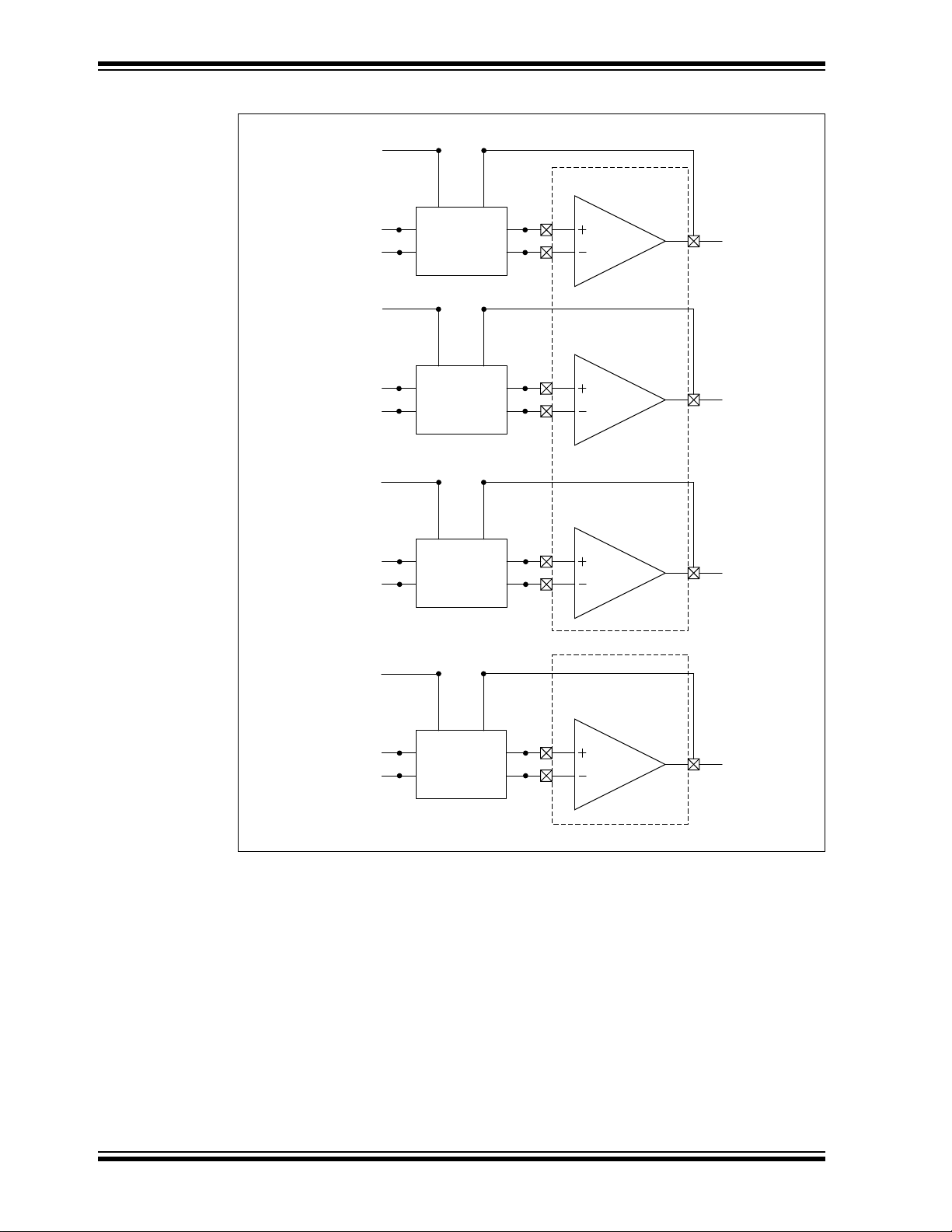
dsPIC33CK Low-Voltage Motor Control Board User’s Guide
Filter,
Feedback and
Bias Circuit
Filter,
Feedback and
Bias Circuit
Filter,
Feedback and
Bias Circuit
MCP6024
IB_EXT
IA_EXT
IC_EXT
VREF
VREF
VREF
SHUNT_IC_N
SHUNT_IC_P
SHUNT_IB_N
SHUNT_IB_P
SHUNT_IA_N
SHUNT_IA_P
Op Amp B
Op Amp A
A
B
D
E
F
U5
A
B
C
A
B
C
E
D
E
1
F
F
3
2
7
5
6
8
10
9
Op Amp C
Filter,
Feedback and
Bias Circuit
IBUS_EXT
VREF
SHUNT_IBUS_N
SHUNT_IBUS_P
F
A
B
CD
E
1
3
4
MCP651S
U15
FIGURE C-2: EXTERNAL CURRENT AMPLIFIERS (U5, U15)
C
D
DS50002927A-page 58 2020 Microchip Technology Inc.
Page 59

Design Details
C2
RIN
RIN
C1
C2
R
F
RF
RIN
RIN
A
B
C
D
E
F
R
IN2
R
IN1
R
IN1
R
IN2
Differential Amplifier Gain =
Rf
(R
IN1
+ R
IN2
)
Differential-mode f
–3dB
1
2(R
IN1
+ R
IN2
)
C2
2
+ C1
Common-mode f
–3dB
1
2(R
IN1
)(C2)
FIGURE C-3: FILTER, FEEDBACK AND BIAS CIRCUIT
Equation C-1 provides the amplifier gain calculations. Equation C-2 and Equation C-3
provide the equations to calculate cutoff frequencies of the Differential-mode and
Common-mode filters.
EQUATION C-1: AMPLIFIER GAIN
EQUATION C-2: CUTOFF FREQUENCY DIFFERENTIAL-MODE FILTER
EQUATION C-3: CUTOFF FREQUENCY COMMON-MODE FILTER
2020 Microchip Technology Inc. DS50002927A-page 59
Page 60

dsPIC33CK Low-Voltage Motor Control Board User’s Guide
Ta bl e C - 1 summarizes the amplifier gain and peak currents for various values of RF.
The customer can select different values, based on application requirements, ensuring
peak current is within the board operating range.
TABLE C-1: EXAMPLE CONFIGURATION – AMPLIFIER GAIN VS. PEAK
CURRENT
Table Summarizes Amplifier Gains and Peak Currents for Various Values of RF when
R
IN1 = 62R, RIN2 = 470R, RSHUNT = 0.01R
F Amplifier Gain
R
20.0 k 37.593 4.389 Amps Peak ERA-3AEB203V
10.0 k 18.796 8.778 Amps Peak ERA-3AEB103V
6.65 k 12.5 13.2 Amps Peak ERA-3AEB6651V
4.99 k 9.379 17.59 Amps Peak ERA-3AEB4991V
4.02 k 7.556 21.83 Amps Peak ERA-3AEB4021V
Peak Current @
1.65V
Rf Resistor Part Number
(use below part number
or similar)
DS50002927A-page 60 2020 Microchip Technology Inc.
Page 61

C.3 AUXILIARY POWER SUPPLY
VIN
+12V
+12V Output
DC-DC
Converter
(MIC28511)
PGND
+5V
+5V Output
DC-DC
Converter
(MCP16301)
DGND
+3.3 VA
+3.3V Output
LDO
(MCP1826)
AGND
+3.3V
DGND
Auxiliary Power Supply
PGND
V
DD
19
PV
DD
20
PV
IN
7
PV
IN
8
PV
IN
9
V
IN
17
FREQ
24
EN
16
DL (NC)
1
DH (NC)
3
SW
12
SW
21
(EPAD3) SW
27
LX
5
PV
IN
4
PVIN (EPAD1)
25
BST
6
I
LIM
18
FB
14
PGOOD
15
AGND
13
PGND
2
PGND
10
PGND
11
PGND
22
PGND
23
(EPAD2) PGND
26
MIC28511
U1
0.1 μF
C2
0.1 μF
C6
100k
R3
PGND
+12V
1.21R
R2
2.2 μF
C1
2.2 μF
C3
100k
R8
100k
R7
DNP
R11
1.21R
R5
2.2 μF
C15
22 μF
C13
BAT46W
D1
10R
R1
DNP
C4
PGND
100 μH
L1
47 μF
C7
2.2 μF
C8
715R
R10
3300 pF
C5
0.1 μF
C22
PGND
1k
R4
PGND
0.1 μF
C30
10k
R6
10k
R9
V
IN
The auxiliary power supply circuit consists of the following three stages (see
Figure C-4):
• +12V Output Power Supply
• +5V Output Power Supply
• +3.3V Output Power Supply
FIGURE C-4: AUXILIARY POWER SUPPLY
Design Details
C.3.1 +12V Output Power Supply
The +12V output power supply is a synchronous buck converter (see Figure C-5)
based on MIC28511. This power supply stage has the following specifications:
• Input Voltage (V
• Output Voltage (labeled as ‘+12V’) = +12V
FIGURE C-5: +12V POWER SUPPLY CIRCUIT
2020 Microchip Technology Inc. DS50002927A-page 61
IN) Range = +14V to +48V
Page 62

dsPIC33CK Low-Voltage Motor Control Board User’s Guide
0.8 R6
V
OUT – VFB
0.8 10k
11.2V
= 714.3
(ICLIM – IL(PP) 0.5) R
DS-ON
+ VCL
ICL
(2A – 0.2 0.5) 28 m + 14 mV
70 µA
= = 960
(VINMAX – VOUT)
IL ILMAX F
SW
= = 88.23 µH
V
OUT
VINMAX
(60V – 12V)
0.2 0.8A kHz
12V
60V
100 µH (0.8A +
(12 + 0.1)
2
– (12)
2
== 32 µF
0.8A 0.2
2
100 µH (0.88)
2
(12.1)2 – (12)
2
L IPK
2
(VOUT + VOUT)2 – VOUT
2
)
2
=
The major components of the +12V supply are:
• The capacitors, C13 and C15, are the input supply capacitors of the +12V power
supply stage.
• The EN pin of the MIC28511 has an on-board 100 k pull-up resistor (R8) to V
which allows the output to be turned on when PV
• The switching frequency of the converter is set by the resistors, R7 and R11.
When R11 is not populated, the switching frequency will typically be 680 kHz, as
is the case in this Motor Control Board. The resistor R7 is selected as 100 k.
• The output is determined by resistors, R6 and R10, where V
V
FB = 0.8V and R6 = 10k. Then, R10 is calculated as:
DD exceeds its UVLO threshold.
OUT = +12V,
IN,
• The MIC28511 uses the R
and a resistor connected from ILIM to the SW node
DS-ON
to decide the current limit. The current limit resistor R4 value is calculated as:
• The Power Good (PGOOD) pin is an open-drain output, which is pulled up with a
10 kΩ resistor (R9) to V
DD. This indicates a logic high when the output is
nominally 90% of its steady-state voltage.
• The bootstrap circuit, the diode D1, resistor R2 and capacitor C2. This circuit
supplies energy to the high-side drive circuit. In the Motor Control Board, D1 is
selected as BAT46W, R2 is set as 10Ω and C2 is selected as 0.1 µF to hold a
charge for approximately 1.25 µSec.
• In order to have some amount of voltage ripple at the voltage feedback pin, a
ripple injection method is applied for low output voltage ripple applications. In the
Motor Control Board, components C5 (3300 pF), R3 (100k) and C6 (0.1 µF) are
used for this purpose.
• The output stage of the synchronous buck converter is comprised of an inductor
and capacitor. In this case, inductor L1 and capacitors, C7 and C2, are the output
inductor and capacitor.
- The minimum value of the inductance at maximum input voltage (i.e., 60V),
considering 20% ripple current is as follows:
DS50002927A-page 62 2020 Microchip Technology Inc.
- The minimum value of the output capacitance can be calculated based on the
selected output inductance L1 (100 µH), which is:
In the Motor Control Board, output capacitors, C7 and C2, are set as 47 µF and
2.2 µF; setting total output capacitor value as greater than the calculated value.
For additional information and recommendations, refer to the “MIC28511 – 60 V
3A Synchronous Buck Regulator Data Sheet” (DS20005520) and “MIC28511-1YFL
Evaluation Board User’s Guide”.
IN,
Page 63

Design Details
DCLOCAL
CIN
MCP16301
V
IN
EN
GND
BOOST
SW
V
FB
DB
RBOOST CB
VBUCK
COUT
RTOP1
RBOT1
D
R
SNU
CSNU
L
R
TOP1
= R
BOT1
V
BUCK
V
FB
– 1
K = V
BUCK
/L
C.3.2 +5V Output Power Supply
The +5V output power supply is a buck converter (see Figure C-6) based on
MCP16301. This power supply stage has the following specifications:
• Input Voltage (V
• Output Voltage (labeled as ‘+5V’) = +5V
FIGURE C-6: +5V POWER SUPPLY
IN) = +12V
The component values used in this circuit are listed in Ta b le C - 2,and were chosen
using Equation C-4 with V
BUCK = +5V, VFB = 0.8V and K = 0.22V/H.
EQUATION C-4:
TABLE C-2: +5V POWER SUPPLY COMPONENT VALUES
Label Component Designator Component Value
R
BOT1 R18 10k
TOP1R14 52.5k
R
LL222 µH
RBOOST R13 82R
B C39 01. µF
C
C
IN C23, C31 20 µF
OUT C100 10 µF
C
SNU R17 4.7R
R
C
SNU C33 120 pF
2020 Microchip Technology Inc. DS50002927A-page 63
Page 64

dsPIC33CK Low-Voltage Motor Control Board User’s Guide
I
D(AVG)
=
V
BUCK
DC
LOCAL
1 –
I
OUT
A low forward drop Schottky diode is used for free-wheeling diode D. The average
diode current is calculated using Equation C-5. Based on these calculations, a
MBRA140T3G Schottky diode is selected.
EQUATION C-5:
A standard 1N4148 ultra-fast diode for boost diode D
B was selected based on
recommendations from the “MCP16301/H High-Voltage Input Integrated Switch
Step-Down Regulator Data Sheet” (DS20005004). For more information about the
snubber circuits, R
SNU and CSNU, and series boost resistor, RBOOST, refer to AN1466,
“Reduction of the High-Frequency Switching Noise in the MCP16301 High-Voltage
Buck Converter” (DS01466) application note.
C.3.3 +3.3V Output Power Supply
The second stage of the power supply has the following specifications:
• Input Voltage = +5.0V
• Output Voltage 1 (+3.3V and +3.3 VA) = +3.3V
The MCP1826 LDO is used for generating the +3.3V output. The input of the +3.3V
LDO is the output of the +5V Converter. In the Motor Control Board, digital supply +3.3V
and analog supply +3.3 VA (see Figure C-7) are separated by the jumper resistor R15.
Similarly, Digital Ground (DGND) and Analog Ground (AGND) are separated by the
jumper resistor R19. This is done to logically divide supply lines to analog and digital
circuits during the board layout design.
DS50002927A-page 64 2020 Microchip Technology Inc.
Page 65

FIGURE C-7: +3.3V POWER SUPPLY
V
IN
V
OUT
+5V
C100
10 µF
C101
10 µF
C102
0.1 µF
C103
0.1 µF
C104
10 µF
C105
10 µF
C106
0.1 µF
V
IN
V
OUT
GND
U12
MCP1826S/3.3V
13
2
DGND
R19
0R
0805
AGND
+3.3V +3.3 VA
R15
0R
0805
Design Details
2020 Microchip Technology Inc. DS50002927A-page 65
Page 66

Worldwide Sales and Service
AMERICAS
Corporate Office
2355 West Chandler Blvd.
Chandler, AZ 85224-6199
Tel: 480-792-7200
Fax: 480-792-7277
Technical Support:
http://www.microchip.com/
support
Web Address:
www.microchip.com
Atlanta
Duluth, GA
Tel: 678-957-9614
Fax: 678-957-1455
Austin, TX
Tel: 512-257-3370
Boston
Westborough, MA
Tel: 774-760-0087
Fax: 774-760-0088
Chicago
Itasca, IL
Tel: 630-285-0071
Fax: 630-285-0075
Dallas
Addison, TX
Tel: 972-818-7423
Fax: 972-818-2924
Detroit
Novi, MI
Tel: 248-848-4000
Houston, TX
Tel: 281-894-5983
Indianapolis
Noblesville, IN
Tel: 317-773-8323
Fax: 317-773-5453
Tel: 317-536-2380
Los Angeles
Mission Viejo, CA
Tel: 949-462-9523
Fax: 949-462-9608
Tel: 951-273-7800
Raleigh, NC
Tel: 919-844-7510
New York, NY
Tel: 631-435-6000
San Jose, CA
Tel: 408-735-9110
Tel: 408-436-4270
Canada - Toronto
Tel: 905-695-1980
Fax: 905-695-2078
ASIA/PACIFIC
Australia - Sydney
Tel: 61-2-9868-6733
China - Beijing
Tel: 86-10-8569-7000
China - Chengdu
Tel: 86-28-8665-5511
China - Chongqing
Tel: 86-23-8980-9588
China - Dongguan
Tel: 86-769-8702-9880
China - Guangzhou
Tel: 86-20-8755-8029
China - Hangzhou
Tel: 86-571-8792-8115
China - Hong Kong SAR
Tel: 852-2943-5100
China - Nanjing
Tel: 86-25-8473-2460
China - Qingdao
Tel: 86-532-8502-7355
China - Shanghai
Tel: 86-21-3326-8000
China - Shenyang
Tel: 86-24-2334-2829
China - Shenzhen
Tel: 86-755-8864-2200
China - Suzhou
Tel: 86-186-6233-1526
China - Wuhan
Tel: 86-27-5980-5300
China - Xian
Tel: 86-29-8833-7252
China - Xiamen
Tel: 86-592-2388138
China - Zhuhai
Tel: 86-756-3210040
ASIA/PACIFIC
India - Bangalore
Tel: 91-80-3090-4444
India - New Delhi
Tel: 91-11-4160-8631
India - Pune
Tel: 91-20-4121-0141
Japan - Osaka
Tel: 81-6-6152-7160
Japan - Tokyo
Tel: 81-3-6880- 3770
Korea - Daegu
Tel: 82-53-744-4301
Korea - Seoul
Tel: 82-2-554-7200
Malaysia - Kuala Lumpur
Tel: 60-3-7651-7906
Malaysia - Penang
Tel: 60-4-227-8870
Philippines - Manila
Tel: 63-2-634-9065
Singapore
Tel: 65-6334-8870
Taiwan - Hsin Chu
Tel: 886-3-577-8366
Taiwan - Kaohsiung
Tel: 886-7-213-7830
Taiwan - Taipei
Tel: 886-2-2508-8600
Thailand - Bangkok
Tel: 66-2-694-1351
Vietnam - Ho Chi Minh
Tel: 84-28-5448-2100
EUROPE
Austria - Wels
Tel: 43-7242-2244-39
Fax: 43-7242-2244-393
Denmark - Copenhagen
Tel: 45-4450-2828
Fax: 45-4485-2829
Finland - Espoo
Tel: 358-9-4520-820
France - Paris
Tel: 33-1-69-53-63-20
Fax: 33-1-69-30-90-79
Germany - Garching
Tel: 49-8931-9700
Germany - Haan
Tel: 49-2129-3766400
Germany - Heilbronn
Tel: 49-7131-72400
Germany - Karlsruhe
Tel: 49-721-625370
Germany - Munich
Tel: 49-89-627-144-0
Fax: 49-89-627-144-44
Germany - Rosenheim
Tel: 49-8031-354-560
Israel - Ra’anana
Tel: 972-9-744-7705
Italy - Milan
Tel: 39-0331-742611
Fax: 39-0331-466781
Italy - Padova
Tel: 39-049-7625286
Netherlands - Drunen
Tel: 31-416-690399
Fax: 31-416-690340
Norway - Trondheim
Tel: 47-7288-4388
Poland - Warsaw
Tel: 48-22-3325737
Romania - Bucharest
Tel: 40-21-407-87-50
Spain - Madrid
Tel: 34-91-708-08-90
Fax: 34-91-708-08-91
Sweden - Gothenberg
Tel: 46-31-704-60-40
Sweden - Stockholm
Tel: 46-8-5090-4654
UK - Wokingham
Tel: 44-118-921-5800
Fax: 44-118-921-5820
DS50002927A-page 66 2020 Microchip Technology Inc.
05/14/19
 Loading...