

Page 1

dsPIC33CK Curiosity
Development Board
User’s Guide
2019 Microchip Technology Inc. DS50002859A
Page 2

Note the following details of the code protection feature on Microchip devices:
YSTEM
CERTIFIED BY DNV
== ISO/TS 16949 ==
• Microchip products meet the specification contained in their particular Microchip Data Sheet.
• Microchip believes that its family of products is one of the most secure families of its kind on the market today, when used in the
intended manner and under normal conditions.
• There are dishonest and possibly illegal methods used to breach the code protection feature. All of these methods, to our
knowledge, require using the Microchip products in a manner outside the operating specifications contained in Microchip’s Data
Sheets. Most likely, the person doing so is engaged in theft of intellectual property.
• Microchip is willing to work with the customer who is concerned about the integrity of their code.
• Neither Microchip nor any other semiconductor manufacturer can guarantee the security of their code. Code protection does not
mean that we are guaranteeing the product as “unbreakable.”
Code protection is constantly evolving. We at Microchip are committed to continuously improving the code protection features of our
products. Attempts to break Microchip’s code protection feature may be a violation of the Digital Millennium Copyright Act. If such acts
allow unauthorized access to your software or other copyrighted work, you may have a right to sue for relief under that Act.
Information contained in this publication regarding device
applications and the like is provided only for your convenience
and may be superseded by updates. It is your responsibility to
ensure that your application meets with your specifications.
MICROCHIP MAKES NO REPRESENTATIONS OR
WARRANTIES OF ANY KIND WHETHER EXPRESS OR
IMPLIED, WRITTEN OR ORAL, STATUTORY OR
OTHERWISE, RELATED TO THE INFORMATION,
INCLUDING BUT NOT LIMITED TO ITS CONDITION,
QUALITY, PERFORMANCE, MERCHANTABILITY OR
FITNESS FOR PURPOSE. Microchip disclaims all liability
arising from this information and its use. Use of Microchip
devices in life support and/or safety applications is entirely at
the buyer’s risk, and the buyer agrees to defend, indemnify and
hold harmless Microchip from any and all damages, claims,
suits, or expenses resulting from such use. No licenses are
conveyed, implicitly or otherwise, under any Microchip
intellectual property rights unless otherwise stated.
Microchip received ISO/TS-16949:2009 certification for its worldwide
headquarters, design and wafer fabrication facilities in Chandler and
Tempe, Arizona; Gresham, Oregon and design centers in California
and India. The Company’s quality system processes and procedures
are for its PIC
devices, Serial EEPROMs, microperipherals, nonvolatile memory and
analog products. In addition, Microchip’s quality system for the design
and manufacture of development systems is ISO 9001:2000 certified.
®
MCUs and dsPIC® DSCs, KEELOQ
®
code hopping
QUALITY MANAGEMENT S
Trademarks
The Microchip name and logo, the Microchip logo, AnyRate, AVR,
AVR logo, AVR Freaks, BitCloud, chipKIT, chipKIT logo,
CryptoMemory, CryptoRF, dsPIC, FlashFlex, flexPWR, Heldo,
JukeBlox, KeeLoq, Kleer, LANCheck, LINK MD, maXStylus,
maXTouch, MediaLB, megaAVR, MOST, MOST logo, MPLAB,
OptoLyzer, PIC, picoPower, PICSTART, PIC32 logo, Prochip
Designer, QTouch, SAM-BA, SpyNIC, SST, SST Logo,
SuperFlash, tinyAVR, UNI/O, and XMEGA are registered
trademarks of Microchip Technology Incorporated in the U.S.A.
and other countries.
ClockWorks, The Embedded Control Solutions Company,
EtherSynch, Hyper Speed Control, HyperLight Load, IntelliMOS,
mTouch, Precision Edge, and Quiet-Wire are registered
trademarks of Microchip Technology Incorporated in the U.S.A.
Adjacent Key Suppression, AKS, Analog-for-the-Digital Age, Any
Capacitor, AnyIn, AnyOut, BodyCom, CodeGuard,
CryptoAuthentication, CryptoAutomotive, CryptoCompanion,
CryptoController, dsPICDEM, dsPICDEM.net, Dynamic Average
Matching, DAM, ECAN, EtherGREEN, In-Circuit Serial
Programming, ICSP, INICnet, Inter-Chip Connectivity,
JitterBlocker, KleerNet, KleerNet logo, memBrain, Mindi, MiWi,
motorBench, MPASM, MPF, MPLAB Certified logo, MPLIB,
MPLINK, MultiTRAK, NetDetach, Omniscient Code Generation,
PICDEM, PICDEM.net, PICkit, PICtail, PowerSmart, PureSilicon,
QMatrix, REAL ICE, Ripple Blocker, SAM-ICE, Serial Quad I/O,
SMART-I.S., SQI, SuperSwitcher, SuperSwitcher II, Total
Endurance, TSHARC, USBCheck, VariSense, ViewSpan,
WiperLock, Wireless DNA, and ZENA are trademarks of
Microchip Technology Incorporated in the U.S.A. and other
countries.
SQTP is a service mark of Microchip Technology Incorporated in
the U.S.A.
Silicon Storage Technology is a registered trademark of
Microchip Technology Inc. in other countries.
GestIC is a registered trademark of Microchip Technology
Germany II GmbH & Co. KG, a subsidiary of Microchip
Technology Inc., in other countries.
All other trademarks mentioned herein are property of their
respective companies.
© 2019, Microchip Technology Incorporated, All Rights Reserved.
ISBN: 978-1-5224-4357-5
DS50002859A-page 2 2019 Microchip Technology Inc.
Page 3

dsPIC33CK CURIOSITY
DEVELOPMENT BOARD
USER’S GUIDE
Table of Contents
Preface ........................................................................................................................... 5
Chapter 1. Overview....................................................................................................... 9
1.1 Introduction ..................................................................................................... 9
Chapter 2. Hardware .................................................................................................... 13
2.1 Powering the Board ...................................................................................... 13
2.1.1 USB Power ................................................................................................ 13
2.1.2 External Power .......................................................................................... 13
2.1.3 mikroBUS™ Power ................................................................................... 13
2.2 Using the Programmed Demo Firmware ...................................................... 13
2.3 Reprogramming and Debugging the dsPIC33CK256MP508 Device ........... 13
2.4 Using the USB-UART Interface .................................................................... 14
2.5 Circuit Details ............................................................................................... 15
2.5.1 Jumpers/Headers/Connectors ................................................................... 15
2.5.2 User Interface (UI) ..................................................................................... 15
2.5.3 ADC Op Amp Analog RC Section ............................................................. 16
Appendix A. Board Layout and Schematics.............................................................. 17
A.1 Pinout ........................................................................................................... 17
A.2 dsPIC33CK Curiosity Development Board Schematics ............................... 20
A.3 dsPIC33CK Curiosity Development Board PCB Layout .............................. 28
Appendix B. Bill of Materials (BOM)........................................................................... 31
B.1 Bill of Materials – dsPIC33CK Curiosity Development Board ...................... 31
Worldwide Sales and Service .................................................................................... 36
2019 Microchip Technology Inc. DS50002859A-page 3
Page 4

dsPIC33CK Curiosity Development Board User’s Guide
NOTES:
DS50002859A-page 4 2019 Microchip Technology Inc.
Page 5

dsPIC33CK CURIOSITY
DEVELOPMENT BOARD
USER’S GUIDE
Preface
NOTICE TO CUSTOMERS
All documentation becomes dated, and this manual is no exception. Microchip tools and
documentation are constantly evolving to meet customer needs, so some actual dialogs
and/or tool descriptions may differ from those in this document. Please refer to our website
(www.microchip.com) to obtain the latest documentation available.
Documents are identified with a “DS” number. This number is located on the bottom of each
page, in front of the page number. The numbering convention for the DS number is
“DSXXXXXXXXA”, where “XXXXXXXX” is the document number and “A” is the revision level
of the document.
For the most up-to-date information on development tools, see the MPLAB
Select the Help menu, and then Topics to open a list of available online help files.
®
IDE online help.
INTRODUCTION
This chapter contains general information that will be useful to know before using the
dsPIC33CK Curiosity Development Board. Items discussed in this chapter include:
• Document Layout
• Conventions Used in this Guide
• Recommended Reading
• The Microchip Website
• Product Change Notification Service
• Customer Support
• Document Revision History
DOCUMENT LAYOUT
This user’s guide provides an overview of the dsPIC33CK Curiosity Development
Board. The document is organized as follows:
• Chapter 1. “Overview” – This chapter introduces the dsPIC33CK Curiosity
Development Board and provides a brief overview of its various features.
• Chapter 2. “Hardware” – This chapter describes how to program/debug the
board using the on-board programmer and the main circuit elements of the board.
• Appendix A. “Board Layout and Schematics” – This appendix provides
schematic diagrams for the dsPIC33CK Curiosity Development Board.
• Appendix B. “Bill of Materials (BOM)” – This appendix provides the component
list used in assembling the board.
2019 Microchip Technology Inc. DS50002859A-page 5
Page 6

dsPIC33CK Curiosity Development Board User’s Guide
CONVENTIONS USED IN THIS GUIDE
This manual uses the following documentation conventions:
DOCUMENTATION CONVENTIONS
Description Represents Examples
Arial font:
Italic characters Referenced books MPLAB® IDE User’s Guide
Emphasized text ...is the only compiler...
Initial caps A window the Output window
A dialog the Settings dialog
A menu selection select Enable Programmer
Quotes A field name in a window or
dialog
Underlined, italic text with
right angle bracket
Bold characters A dialog button Click OK
N‘Rnnnn A number in verilog format,
Text in angle brackets < > A key on the keyboard Press <Enter>, <F1>
Courier New font:
Plain Courier New Sample source code #define START
Italic Courier New A variable argument file.o, where file can be
Square brackets [ ] Optional arguments mcc18 [options] file
Curly brackets and pipe
character: { | }
Ellipses... Replaces repeated text var_name [,
A menu path File>Save
A tab Click the Power tab
where N is the total number of
digits, R is the radix and n is a
digit.
Filenames autoexec.bat
File paths c:\mcc18\h
Keywords _asm, _endasm, static
Command-line options -Opa+, -Opa-
Bit values 0, 1
Constants 0xFF, ‘A’
Choice of mutually exclusive
arguments; an OR selection
Represents code supplied by
user
“Save project before build”
4‘b0010, 2‘hF1
any valid filename
[options]
errorlevel {0|1}
var_name...]
void main (void)
{ ...
}
DS50002859A-page 6 2019 Microchip Technology Inc.
Page 7

RECOMMENDED READING
This user’s guide describes how to use the dsPIC33CK Curiosity Development Board.
The device-specific data sheets contain current information on programming the
specific microcontroller or Digital Signal Controller (DSC) devices. The following
Microchip documents are recommended as supplemental reference resources:
MPLAB
This comprehensive guide describes the usage, operation and features of Microchip’s
MPLAB XC16 C compiler (formerly MPLAB C30) for use with 16-bit devices.
MPLAB
This document describes the installation and implementation of the MPLAB X IDE
software.
dsPIC33CK256MP508 Family Data Sheet (DS70005349)
Refer to this document for detailed information on the dsPIC33CK single core Digital
Signal Controllers (DSCs). Reference information found in this data sheet includes:
• Device memory maps
• Device pinout and packaging details
• Device electrical specifications
• List of peripherals included on the devices
and are available for download from the Microchip website (www.microchip.com).
®
XC16 C Compiler User’s Guide (DS50002071)
®
X IDE User’s Guide (DS50002027)
Preface
THE MICROCHIP WEBSITE
Microchip provides online support via our website at www.microchip.com. This website
is used as a means to make files and information easily available to customers.
Accessible by using your favorite Internet browser, the website contains the following
information:
• Product Support – Data sheets and errata, application notes and sample
programs, design resources, user’s guides and hardware support documents,
latest software releases and archived software
• General Technical Support – Frequently Asked Questions (FAQs), technical
support requests, online discussion groups, Microchip consultant program
member listing
• Business of Microchip – Product selector and ordering guides, latest Microchip
press releases, listing of seminars and events; and listings of Microchip sales
offices, distributors and factory representatives
PRODUCT CHANGE NOTIFICATION SERVICE
Microchip’s customer notification service helps keep customers current on Microchip
products. Subscribers will receive e-mail notification whenever there are changes,
updates, revisions or errata related to a specified product family or development tool of
interest.
To register, access the Microchip website at www.microchip.com, click on Product
Change Notification and follow the registration instructions.
2019 Microchip Technology Inc. DS50002859A-page 7
Page 8

dsPIC33CK Curiosity Development Board User’s Guide
CUSTOMER SUPPORT
Users of Microchip products can receive assistance through several channels:
• Distributor or Representative
• Local Sales Office
• Corporate Application Engineer (CAE)
• Embedded Solutions Engineer (ESE)
• Field Application Engineer (FAE)
Customers should contact their distributor, representative or Embedded Solutions
Engineer (ESE) for support. Local sales offices are also available to help customers.
A listing of sales offices and locations is included in the back of this document.
Technical support is available through the website at:
http://www.microchip.com/support.
DOCUMENT REVISION HISTORY
Revision A (April 2019)
This is the initial release of this document.
DS50002859A-page 8 2019 Microchip Technology Inc.
Page 9

1.1 INTRODUCTION
2
3
3
1
9
7
10
5
6
8
4
12
11
13
14
10
The dsPIC33CK Curiosity Development Board (DM330030) is intended as a
cost-effective development and demonstration platform for the dsPIC33CK256MP508
family of single core, high-performance Digital Signal Controllers (DSCs). The main
hardware features of the board are highlighted in Figure 1-1.
FIGURE 1-1: dsPIC33CK CURIOSITY DEVELOPMENT BOARD
dsPIC33CK CURIOSITY
DEVELOPMENT BOARD
USER’S GUIDE
Chapter 1. Overview
1. dsPIC33CK256MP508 single core, 16-bit Digital Signal Processor (DSP) target
device.
2. Integrated PICkit™ On-Board 4 (PKOB4) programmer/debugger.
3. 2x mikroBUS™ interfaces for hardware expansion, compatible with a wide range
of existing click boards™ from MikroElektronika (www.mikroe.com).
4. 1x Red/Green/Blue (RGB) LED.
5. 2x general purpose orange indicator LEDs.
6. 3x general purpose push buttons.
2019 Microchip Technology Inc. DS50002859A-page 9
7. 1x MCLR
8. 10k potentiometer.
9. USB to UART interface.
10. Female, 100 mil pitch, I/O pin access headers for probing and connecting to all
target microcontroller GPIO pins.
Reset push button.
Page 10

dsPIC33CK Curiosity Development Board User’s Guide
11. Configurable jumper (J11) for selecting +5V USB power or +5V external power.
12. Analog input section for dedicated ADC Core 0, Core 1 and shared core.
13. ADC reference generator MCP6021 op amp.
14. dsPIC33CK LDO.
Figure 1-2 and Figure 1-3 show the block diagrams of the dsPIC33CK Curiosity
Development Board and the PKOB main system. For more detailed schematics, refer
to Appendix A. “Board Layout and Schematics”.
DS50002859A-page 10 2019 Microchip Technology Inc.
Page 11

2019 Microchip Technology Inc. DS50002859A-page 11
T_ICSP
dsPIC_UART
Digital
Analog
MCLR
MCPINS
Control
T_ICSP
USB_PKOB
dsPIC_UART
PICkit™ On-Board
USB
ICSP™
dsPIC_UART
USB_PKOB
MCLR
Communication
+3.3V
+5V_USB
History
Analog
Digital
MCLR
Interfaces
MCPINS
Internal_OpAmp_RC
MCLR
USB_PGD
PG_SYSTEM
USB_POWER
03-10882_2.0_PKOB_USB_Power.SchDoc
USB_PGD
VPP_ON
PG_SYSTEM
TVDD_GOOD
dsPIC_UART
DBG_ICSP
USB_PKOB
PKOB4 MICRO
03-10882_2.0_PKOB_Main_Micro.SchDoc
TVDDTVPP
DBG_ICSP
TVDD_GOOD
T_ICSP
VPP_ON
DRIVER -BUILTIN
03-10882_2.0_PKOB_PinDriver.SchDoc
TVDD_GOOD
TVDDTVPP
TVDD_GOOD
T_ICSP
To Control
USB_PKOB
To Communication
Target ICSP™ Signals
0R 0402
R80P
TVDD
+3.3V
GND_PK
0R 0603
R81P
GND_U
PG_SYSTEM
VPP_ON
dsPIC_UART
FIGURE 1-2: dsPIC33CK CURIOSITY DEVELOPMENT BOARD BLOCK DIAGRAM
FIGURE 1-3: PKOB MAIN SYSTEM INTERCONNECT
Overview
Page 12

dsPIC33CK Curiosity Development Board User’s Guide
NOTES:
DS50002859A-page 12 2019 Microchip Technology Inc.
Page 13

Chapter 2. Hardware
2.1 POWERING THE BOARD
2.1.1 USB Power
This board is intended to be primarily powered from the USB Micro-B connector, J7.
The official “USB 2.0 Specification” restricts USB applications to consuming no more
than 500 mA of USB V
2.1.2 External Power
An external +5 VDC may optionally be connected through the J2, J4 100 mil connector,
and the 2-pin jumper should be moved from +5V USB to +5V external power on the J11
3-pin connector.
An external +3.3 V
connector to power an external circuit from the dsPIC33CK LDO. However, a maximum
of 50 mA consumption is recommended.
dsPIC33CK CURIOSITY
DEVELOPMENT BOARD
USER’S GUIDE
BUS power from the host.
DC may optionally be connected through the J1, J3 100 mil
2.1.3 mikroBUS™ Power
An external +5 VDC may optionally be connected through the J2, J4 100 mil connector.
In this case, the 2-pin jumper should be moved from +5V USB to +5V external power
on the J11 3-pin connector. A maximum of 400 mA is recommended to be supplied to
the mikroBUS click boards™.
The mikroBUS +3.3 V
can supply up to 500 mA.
DC power is connected to the +3V3PK on the PKOB4 LDO, which
2.2 USING THE PROGRAMMED DEMO FIRMWARE
The development board comes programmed with some basic demo firmware, which
exercises several of the board hardware features. The demo project for the dsPIC33CK
Curiosity Development Board implements an RGB color mixing application. In the
demo, the potentiometer can be used to adjust each color channel intensity
independently, while the push buttons are used to select the channel to be adjusted.
The source code for the demo can be obtained from:
www.microchip.com/dspic33ckcuriosity
2.3 REPROGRAMMING AND DEBUGGING THE dsPIC33CK256MP508 DEVICE
The board has a PICkit™ On-Board (PKOB) programmer/debugger circuit, which can
be used to program and debug the dsPIC33CK256MP508 target device (U1).
Alternatively, an external programmer/debugger tool can be connected to the board via
the 6-pin in-line connector J8, using a male-male 100 mil pitch 6-pin header.
2019 Microchip Technology Inc. DS50002859A-page 13
Page 14
dsPIC33CK Curiosity Development Board User’s Guide
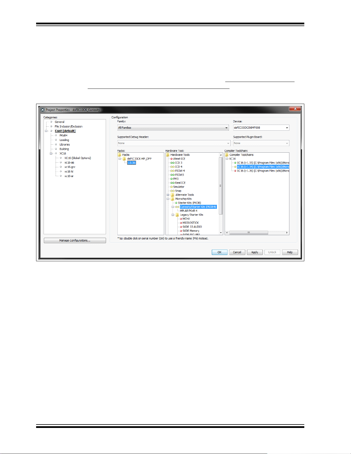
The PKOB circuit should automatically enumerate and be recognized by the
MPLAB
the host via the USB Micro-B connector, J7. No custom USB driver installation is
necessary as the PKOB circuit relies on standard OS provided Human Interface Device
(HID) drivers, and therefore, the driver installation should be fully automatic. When
plugged in, the PKOB programmer/debugger tool can be selected from the MPLAB X
project properties page by selecting the device under: Hardware Tools>Microchip
Kits>Starter Kits (PKOB)>Curiosity/Starter Kits (PKOB4), as shown in Figure 2-1.
FIGURE 2-1: dsPIC33CK CURIOSITY PKOB TOOL SELECTION
®
X IDE, v5.05 or later, when the dsPIC33CK Curiosity Board is connected to
2.4 USING THE USB-UART INTERFACE
The board is equipped with a USB-UART interface based around the MCP2221A chip.
The MCP2221A chip implements the standard Communication Device Class (CDC) –
Abstract Control Model (ACM) protocol, and therefore, can use standard USB drivers
that are provided with modern Windows
most operating systems, the USB driver installation will be fully automatic. Under certain older operating systems, or if the device is attached to an older than Windows 10
machine without an active Internet connection, manual installation of the drivers may
be necessary. In this case, the driver package can be downloaded from:
www.microchip.com/mcp2221a
Details on how to access the serial port from Mac and Linux operating systems can also
be found in the associated collateral for the MCP2221A. Under Windows, after
successful USB driver installation, the device will appear as a “COMx” port object,
which standard serial terminal programs can open/read/write to and from.
DS50002859A-page 14 2019 Microchip Technology Inc.
®
, Mac® and Linux® operating systems. Under
Page 15

2.5 CIRCUIT DETAILS
This section highlights some of the circuit elements and provides an explanation for
their intent and function.
2.5.1 Jumpers/Headers/Connectors
J1, J3 – These are populated 2x25-pin, 100 mil jumper headers, in which a power
module or any other custom designed board may optionally be inserted to access the
microcontroller’s digital pins. Use the triangle alignment mark on J1, pin 1 (underneath
V
REF, see Figure 1-1) to connect the dsPIC33CK Curiosity Development Board to other
boards.
J2, J4 – These are populated 2x25-pin, 100 mil jumper headers, in which a power
module or any other custom designed board may optionally be inserted to access the
microcontroller’s analog and digital pins.
J5, J6 – These are female headers that implement the mikroBUS Interfaces A and B,
which are used to attach hardware daughter boards to expand the functionality of the
development board.
J7 – This is a standard female USB Micro-B connector, which connects to the
MCP2221A USB-UART converter chip and the on-board MPLAB PKOB4
programmer/debugger. This USB interface has a data interface and supplies power to
the rest of the board, as well as to the mikroBUS A and B, up to 400 mA.
J8 – This is an unpopulated 6-pin staggered header interface that can optionally be
used to connect an external programmer/debugger to the target microcontroller, U1.
The J8 header connects to the debug port, PGx3. The holes are slightly staggered,
which provides some friction retention force without requiring physical soldering when
a straight male-male or right-angle male-male header is installed into J8.
J9 – This is an unpopulated 2-pin, 100 mil jumper header, which may optionally be used
to insert a current meter in series with the U1 V
microcontroller’s current consumption. In order to measure the U1 current, the trace
(NT1) on the bottom of the PCB, that shorts the two pins of J1, should be cut and a
2-pin jumper should be soldered into J9.
J10, J12 – These are populated 2x2-pin, 100 mil jumper headers, which may optionally
be used to insert GND_D of a power module or any other custom designed boards that
access the microcontroller’s analog and digital pins. Also, it has the purpose of a
mechanical key that will prevent reverse connection.
DD current path to measure the
2.5.2 User Interface (UI)
The dsPIC33CK Curiosity Board contains a User Interface (UI), easily accessible on
the right side (see Figure 1-1). The UI has the following elements:
• One RGB LED
• A 10K Potentiometer
• Three Push Buttons
• Two Debug Orange LEDs
Each element can be programed for any purpose to create the desired interaction
between the user and the board behavior.
2019 Microchip Technology Inc. DS50002859A-page 15
Page 16

dsPIC33CK Curiosity Development Board User’s Guide
F
c
1
2RC
-------------- -=
t
r
2.197=
2.5.3 ADC Op Amp Analog RC Section
The board contains three RC filter components for each individual ADC core of the
microcontroller, U1. They are identical; the only difference is that one connects to the
dedicated ADC Core 1, another to the dedicated ADC Core 0 and the third one to the
shared ADC core.
The default configuration is the internal op amp variant, in which all passive
components, R and C, are populated for the filter, feedback and bias circuits.
To use the external op amp, remove R59, R75 and R81 resistors and populate C24,
C25 and C26 with 5600 pF, 50V, 0603, COG resistors to enable an RC filter of
F
C = 506 kHz.
There is an on-board MCP6021 op amp to power the internal V
op amps with 1.65V (V
V
REF_EXT can also be used from connector J2 by removing, R30, 75 Ohm, and moving
it into the R31 place (default DNP).
The RC filters have a cutoff frequency:
EQUATION 2-1:
DD/2) voltage reference.
REF for the three
where R is the resistance and C is the capacitor of the filter.
Example: R = 56 Ohms and C = 5600 pF, then F
Rise/fall time, with a steady state of 10% to 90%, is proportional to the time constant:
= RC.
EQUATION 2-2:
For example: R = 56 Ohms and C = 5600 pF, then t
C = 507509 [Hz] or 507 [kHz].
= 0.68 µs.
r
DS50002859A-page 16 2019 Microchip Technology Inc.
Page 17

dsPIC33CK CURIOSITY
DEVELOPMENT BOARD
USER’S GUIDE
Appendix A. Board Layout and Schematics
This appendix contains the pinout, the schematics and the board layouts for the
dsPIC33CK Curiosity Board. The topics covered in this appendix include:
• Pinout
• dsPIC33CK Curiosity Development Board Schematics
• dsPIC33CK Curiosity Development Board PCB Layout
A.1 PINOUT
Ta bl e A -1 and Tab le A -2 show the pinout and the electrical parameters for connectors,
J1 and J2, respectively.
TABLE A-1: PINOUT AND ELECTRICAL PARAMETERS, J1
Name J1 dsPIC® DSC Pin Function/Description Remark
VREF_EXT 1 NC — —
+3.3V 2 12, 31, 51, 71 dsPIC DSC VDD Supply Output Limit 50 mA
NC 3 NC — —
GND_A 4 26 Analog Ground —
AN12_RP48 5 15 Analog Input —
IA_AN0_OA1OUT 6 16 Analog Input, 56R, Cap = DNP F
IB_AN1_OA2OUT 7 41 Analog Input, 56R, Cap = DNP FC = 507 kHz, tr = 0.68 μs
S_ANA1_OA2IN- 8 18 Analog Input 2 k in series
S_AN8_OA2IN- 9 43 Analog Input 2 k in series
S_AN9_OA1IN+ 10 20 Analog Input 2 k in series
S_RB4_OA2IN+ 11 45 Analog Input 2 k in series
AN17_RP54 12 30 Analog Input —
AN2_CMP3A 13 58 Analog Input Comparator 3
IBUS_AN4_OA3OUT 14 23 Analog Input, 56R Cap = DNP F
AN10_PGD1 15 60 Analog Input —
S_AN13_OA3IN- 16 28 Analog Input 2 k in series
AN15_CMP2A 17 33 Analog Input Comparator 2
S_AN14_OA3IN+ 18 29 Analog Input 2 k in series
AN18_CMP3C 19 38 Analog Input Comparator 3
AN3_DACOUT1 20 21 Analog Input DAC output
AN20_RE0 21 2 MikroA Analog Pin —
AN6_RP33 22 35 Analog Input —
AN22_RE2 23 17 MikroB Analog Pin —
AN11_PGC1 24 61 MikroA Reset —
RP77_ANN2 25 14 Analog Input —
AN16_RP55 26 40 Temp. Input, RC Filtered F
NC 27 NC Not Connected Reserved for future use
AN19_CMP2C 28 36 Analog Input Comparator 2
C = 507 kHz, t
C = 507 kHz, t
C = 159 Hz, t
= 0.68 μs
r
= 0.68 μs
r
= 2.1 ms
r
2019 Microchip Technology Inc. DS50002859A-page 17
Page 18

dsPIC33CK Curiosity Development Board User’s Guide
TABLE A-1: PINOUT AND ELECTRICAL PARAMETERS, J1 (CONTINUED)
Name J1 dsPIC® DSC Pin Function/Description Remark
NC 29 NC Not Connected Reserved for future use
AN21_RE1 30 4 VBUS Input, RC Filtered FC = 1.4 kHz, tr = 24 μs
NC 31 NC Not Connected Reserved for future use
AN23_RE3 32 19 Pot. Input, RC Filtered F
NC 33 — Not Connected Reserved for future use
NC 34 — Not Connected Reserved for future use
NC 35 — Not Connected Reserved for future use
NC 36 — Not Connected Reserved for future use
NC 37 — Not Connected Reserved for future use
NC 38 — Not Connected Reserved for future use
NC 39 — Not Connected Reserved for future use
NC 40 — Not Connected Reserved for future use
NC 41 — Not Connected Reserved for future use
2
ASCL1_RP57 42 47 mikroBUS™ I
ASDA1_RP56 43 46 mikroBUS I2C, SDA Parallel MikroA, MikroB
NC 44 NC Not Connected Reserved for future use
NC 45 NC Not Connected Reserved for future use
SCL2_PGC3 46 56 Program/Debug PGC
SDA2_PGD3 47 55 Program/Debug PGD
MCLR
GND_D 49 11, 32, 50, 70 Digital Ground —
GND_D 50 11, 32, 50, 70 Digital Ground —
48 9 Device Reset 0R series resistance
C, SCL Parallel MikroA, MikroB
C = 4.8 kHz, t
= 72 μs
r
TABLE A-2: PINOUT AND ELECTRICAL PARAMETERS, J2
Name J2 dsPIC® DSC Pin Function/Description Remark
RP47_PWM1L 1 3 PWM Output 75R series resistance
RP46_PWM1H 2 1 PWM Output 75R series resistance
RP45_PWM2L 3 80 PWM Output 75R series resistance
RP44_PWM2H 4 78 PWM Output 75R series resistance
RP43_PWM3L 5 76 PWM Output 75R series resistance
RP42_PWM3H 6 75 PWM Output 75R series resistance
RP64_PWM4L 7 74 PWM Output 75R series resistance
RP65_PWM4H 8 73 PWM Output 75R series resistance
RP53_PWM5L 9 65 PWM Output 75R series resistance
RP52_PWM5H 10 63 PWM Output 75R series resistance
RP63_PWM6L 11 8 PWM Output 75R series resistance
RP62_PWM6H 12 7 PWM Output 75R series resistance
RP59_PWM7L 13 67 PWM Output 75R series resistance
RP58_PWM7H 14 66 PWM Output 75R series resistance
RP61_PWM8L 15 6 PWM Output 75R series resistance
RP60_PWM8H 16 5 PWM Output 75R series resistance
NC 17 — Not Connected Reserved for future use
NC 18 — Not Connected Reserved for future use
NC 19 — Not Connected Reserved for future use
DS50002859A-page 18 2019 Microchip Technology Inc.
Page 19

Board Layout and Schematics
TABLE A-2: PINOUT AND ELECTRICAL PARAMETERS, J2 (CONTINUED)
Name J2 dsPIC® DSC Pin Function/Description Remark
NC 20 — Not Connected Reserved for future use
NC 21 — Not Connected Reserved for future use
NC 22 — Not Connected Reserved for future use
NC 23 — Not Connected Reserved for future use
RE15_RGB_R 24 79 RGB LED Red —
RP79_RD15 25 10 MikroA UART RX —
RE14_RGB_G 26 77 RGB LED Green —
RP78_RD14 27 13 MikroA UART TX —
RE13_RGB_B 28 64 RGB LED Blue —
RP76_RD12 29 27 MikroB UART RX 100 in series
RE12_MikroB_INT 30 62 MikroB Interrupt 1 k in series
RP73_RD9 31 48 MikroB UART TX —
RE11_MikroA_INT 32 59 MikroA Interrupt 1 k in series
RP72_RD8 33 49 mikroBUS™ SPI SCK Parallel MikroA, MikroB
RE10_MikroB_CS 34 57 MikroB CS Chip Select —
RP71_RD7 35 52 mikroBUS SPI MISO Parallel MikroA, MikroB
RE9_S3 36 44 User Switch S3 —
RP70_RD6 37 53 mikroBUS SPI MOSI Parallel MikroA, MikroB
RE8_S2 38 42 User Switch S2 —
RP69_RD5 39 54 Digital General Purpose —
RE7_S1 40 39 User Switch S1 —
RP68_RD4_UART_TX 41 68 UART Transmit MCP2221A —
RE6_LED1 42 37 Debug LED1 —
RP67_RD3_UART_RX 43 69 UART Receive MCP2221A —
RE5_LED2 44 24 Debug LED2 —
RP66_RD2_MikroA_CS 45 72 MikroA CS Chip Select —
RE4 46 22 MikroB Reset —
+5V_EXT 47 — Input External Power Selectable via J11
+5V_EXT 48 — Input External Power Selectable via J11
GND_D 49 11, 32, 50, 70 Digital Ground —
GND_D 50 11, 32, 50, 70 Digital Ground —
2019 Microchip Technology Inc. DS50002859A-page 19
Page 20

Designed with
Altium.com
GND_S
+5V_USB
USB_N
USB_P
GND_U GND_U
VDD33
1
VDD33
9
VDD33
18
XTALIN/CLKIN
22
XTALOUT
21
OCS_N1
8
OCS_N2
12
USBDM_UP
19
USBDP_UP
20
NON_REM1/SMBDATA
13
SUSP_IND/NON-REM0
17
RESET_N
15
CFG_SEL0/SMBCLK
14
Vss/PAD
25
VBUS_DET
16
PRTPWR1
7
PRTPWR2
11
USBDM_DN1
2
USBDP_DN1
3
USBDM_DN2
4
USBDP_DN2
5
CRFILT
10
PLLFILT
23
RBIAS
24
NC
6
USB2422T-I/MJ
U60
USB_UART_D_P
USB_UART_D_N
GND_U
USB_PKOB_D_P
USB_PKOB_D_N
USB_PKOB
USB_PKOB_D_P
USB_PKOB_D_N
USB_PKOB
GND_U GND_U
GND_U
GND_U
3V3PK
3V3PK
1M
0603
1%
R157
10 μF
10V
0603
C42
GND_U
To Control
To PKOB
USB/UART Interface
2-Port USB HUB
0.1 μF
16V
0402
C112
1%330R
0603
R160
1%330R
0603
R161
GND_U
GND_U
0.1 μF
16V
0402
C29
1%
10k 0402
R29
dsPIC_UART
dsPIC_UART_TX
dsPIC_UART_RX
dsPIC_UART
USB_UART_D_P
USB_UART_D_N
USB_PKOB_D_P
USB_PKOB_D_N
USB_PKOB_D_P
USB_PKOB_D_NUSB_N
USB_P
For bypassing the USB hub
15R
0603
1%
DNP
R64
15R
0603
1%
DNP
R65
GND_UGND_U
3V3PK
GND_U
V
DD
16
GP0
1
GP1
2
RST
3
UART RX
4
UART TX
5
GP2
6
GP3
7
SDA
8
SCL
9
V
USB
10
D-
11
D+
12
Vss
13
EP
17
NC
14
NC
15
MCP2221A
U4
GREEN
0603
LD3
YELLOW
0603
LD4
3V3PK
1 2 3 4 50
DNGV5+-D+DDI
Micro-AB Receptacle
J7
USB 2.0 MICRO-B FEMALE
1
2
3
4
5
6
82400152
D1
USB Port
600R 0603
1A
FB3
GND_U
GND_D
MCLR
10 μF
10V
0603
C14
10 μF
10V
0603
C20
MCLR
To Control
+3.3V LDO
TP PAD PCB 1.2x0.7
TP3
TP PAD PCB 1.2x0.7
TP4
GND_D
+5V_USB
GREEN
0603
LD1
+5V_EXT
GREEN
0603
LD2
PWRGD is an open-drain output
Place close to the DSP
V
IN
1
SHDN
3
GND
2
PWRGD
4
V
OUT
5
MCP1755/3.3V SOT-23
U2
+3.3V
123
HDR-2.54 Male 1x3
J11
Shunt 2.54 mm 1x2 Handle
JP1
+5V
To be placed on pin 2-3
GND_U GND_D
0R 0603
R66
USBD_N
USBD_P
24 MHz
Y2
0.1 μF
16V
0402
C31
0.1 μF
16V
0402
C32
0.1 μF
16V
0402
C33
1 μF
16V
0402
C30
1 μF
16V
0402
C28
1 μF
16V
0402
C27
18 pF
50V
0402
C41
18 pF
50V
0402
C39
56k
0402
1%
R67
56k
0402
1%
R68
56k
0402
1%
R69
100k
0402
1%
R72
100k
0402
1%
R71
GND_D
Bottom_Shield GND_D
0R 0603
R86
GND_U
10k
0402
1%
R159
10k
0402
1%
R70
15R 0603
R150
15R 0603
R151
3.3k
0402
1%
R32
3.3k
0402
1%
R33
470R
0402
R55
470R
0402
R54
DS50002859A-page 20 2019 Microchip Technology Inc.
A.2 dsPIC33CK CURIOSITY DEVELOPMENT BOARD SCHEMATICS
Figure A-1 through Figure A-8 show the board schematics.
FIGURE A-1: dsPIC33CK CURIOSITY DEVELOPMENT BOARD SCHEMATICS, REV. 2.0 (PAGE 1 OF 8)
dsPIC33CK Curiosity Development Board User’s Guide
Page 21

2019 Microchip Technology Inc. DS50002859A-page 21
Designed with
Altium.com
12
DNP
J9
Net Tie
NT1
VPP/MCLR
V
DD
GND
ICSPCLK
NC
ICSPDAT
Current measurement point
(Local VDD/VSS bypass/decoupling for U1)
RP46/PWM1H/PMD5/RB14
1
AN20/RE0
2
RP47/PWM1L/PMD6/RB15
3
AN21/RE1
4
RP60/PWM8H/PMD7/RC12
5
RP61/PWM8L/PMA5/RC13
6
RP62/PWM6H/PMA4/RC14
7
RP63/PWM6L/PMA3/RC15
8
MCLR
9
RP79/PCI22/PMA2/RD15
10
Vss
11
V
DD
12
RP78/PCI21/RD14
13
ANN2/RP77/RD13
14
AN12/ANN0/RP48/RC0
15
OA1OUT/AN0/CMP1A/IBIAS0/RA0
16
AN22/RE2
17
OA1IN-/ANA1/RA1
18
AN23/RE3
19
OA1IN+/AN9/PMA6/RA2
20
DACOUT1/AN3/CMP1C/RA3
21
RE4
22
OA3OUT/AN4/CMP3B/IBIAS3/RA4
23
RE5
24
AV
DD
25
AVss
26
RP76/RD12
27
OA3IN-/AN13/CMP1B/ISRC0/RP49/PMA7/RC1
28
OA3IN+/AN14/CMP2B/ISRC1/RP50/PMD13/PMA13/RC2
29
AN17/ANN1/IBIAS1/RP54/PMD12/PMA12/RC6
30
V
DD
31
Vss
32
AN15/CMP2A/IBIAS2/RP51/PMD11/PMA11/RC3
33
OSCI/CLKI/AN5/RP32/PMD10/PMA10/RB0
34
OSCO/CLKO/AN6/RP33/PMA1/PMALH/PSA1/RB1
35
AN19/CMP2C/RP75/PMA0/PMALL/PSA0/RD11
36
RE6
37
AN18/CMP3C/ISRC3/RP74/PMD9/PMA9/RD10
38
RE7
39
AN16/ISRC2/RP55/PMD8/PMA8/RC7
40
OA2OUT/AN1/AN7/ANA0/CMP1D/CMP2D/CMP3D/RP34/SCL3/INT0/RB2
41
RE8
42
PGD2/OA2IN-/AN8/RP35/RB3
43
RE9
44
PGC2/OA2IN+/RP36/RB4
45
RP56/ASDA1/SCK2/RC8
46
RP57/ASCL1/SDI2/RC9
47
RP73/PCI20/RD9
48
RP72/SDO2/PCI19/RD8
49
Vss
50
V
DD
51
RP71/PMD15/RD7
52
RP70/PMD14/RD6
53
RP69/PMA15/PMCS2/RD5
54
PGD3/RP37/SDA2/PMA14/PMCS1/PSCS/RB5
55
PGC3/RP38/SCL2/RB6
56
RE10
57
TDO/AN2/CMP3A/RP39/SDA3/RB7
58
RE11
59
PGD1/AN10/RP40/SCL1/RB8
60
PGC1/AN11/RP41/SDA1/RB9
61
RE12
62
RP52/PWM5H/ASDA2/RC4
63
RE13
64
RP53/PWM5L/ASCL2/PMWR/PMENB/PSWR/RC5
65
RP58/PWM7H/PMRD/PMWR/PSRD/RC10
66
RP59/PWM7L/RC11
67
RP68/ASDA3/RD4
68
RP67/ASCL3/RD3
69
Vss
70
V
DD
71
RP66/RD2
72
RP65/PWM4H/RD1
73
RP64/PWM4L/PMD0/RD0
74
TMS/RP42/PWM3H/PMD1/RB10
75
TCK/RP43/PWM3L/PMD2/RB11
76
RE14
77
TDI/RP44/PWM2H/PMD3/RB12
78
RE15
79
RP45/PWM2L/PMD4/RB13
80
dsPIC33CK256MP508
U1
ICSP™ Programming
Master Programming/Debug (also connects to PKOB)
GND_D
GND_D
GND_D GND_D GND_D
GND_D
+3.3V
+3.3V
SCL2_PGC3
SDA2_PGD3
T_ICSP
TARGET_PGD1
TARGET_PGC1
TARGET_MCLR
T_ICSP
GND_A
GND_A
10uF
10V
0603
C10
600R
0603
1A
FB1
0R
0603
R11
RB0_CLKI
RE9_S3
RE8_S2
RE7_S1
RP69_RD5
RP70_RD6
RP71_RD7
RP72_RD8
RP73_RD9
AN18_CMP3C
AN19_CMP2C
RP76_RD12
RP67_RD3_UART_RX
RP68_RD4_UART_TX
RP64_PWM4L
RP65_PWM4H
RP77_ANN2
RP78_RD14
RP79_RD15
RP66_RD2_MikroA_CS
AN20_RE0
AN21_RE1
AN22_RE2
AN23_RE3
RE4
RE5_LED2
RE6_LED1
RE10_MikroB_CS
RE11_MikroA_INT
RE12_MikroB_INT
RE13_RGB_B
RE14_RGB_G
RE15_RGB_R
AN0_OA1OUT
ANA1_OA1INAN9_OA1IN+
AN3_DACOUT1
AN4_OA3OUT
AN6_RP33
AN1_OA2OUT
AN8_OA2INRB4_OA2IN+
SDA2_PGD3
SCL2_PGC3
AN2_CMP3A
AN10_PGD1
AN11_PGC1
RP42_PWM3H
RP43_PWM3L
RP44_PWM2H
RP45_PWM2L
RP46_PWM1H
RP47_PWM1L
AN12_RP48
AN13_OA3INAN14_OA3IN+
AN15_CMP2A
RP52_PWM5H
RP53_PWM5L
AN17_RP54
AN16_RP55
ASDA1_RP56
ASCL1_RP57
RP58_PWM7H
RP59_PWM7L
RP60_PWM8H
RP61_PWM8L
RP62_PWM6H
RP63_PWM6L
+3.3V
Potentiometer
10k
P090S
20%
2
1
3
R17
0.1 μF
16V
0402
C2
AN23_RE3
75R
R51
75R
R50
75R
R43
75R
R42
75R
R44
75R
R45
75R
R46
75R
R47
75R
R48
75R
R49
75R
R37
75R
R36
75R
R38
75R
R39
75R
R40
75R
R41
dsPIC_UART
dsPIC_UART_TX
dsPIC_UART_RX
MCLR
0.1 μF
16V
0402
C18
fc = 1.4 kHz at 1.1k
Thevenin Resistance
AN21_RE1 AN21_VBUS
0.1uF
16V
0402
C19
fc = 160 Hz
for R = 10k
temperature
AN16_RP55 AN16_TEMP
Temperature Sensor
V
BUS
Debug LEDs
GND_D GND_D
YELLOW
0603
LED1
YELLOW
0603
LED2
RE6_LED1
RE5_LED2
2
1
4
3
GREEN
RED
BLUE
5
6
LED3
LED_RGB
RGB LED
330R
R15
GND_D
330R
R14
330R
R13
RE13_RGB_B
RE14_RGB_G
RE15_RGB_R
1 4
2 3
S2
1 4
2 3
S1
10k
1%
R5
10k
1%
R3
+3.3V
+3.3V
Buttons
10k
1%
R7
1 4
2 3
S3
+3.3V
1k
0603
1%
R8
1k
0603
1%
R6
1k
0603
1%
R4
GND_D
GND_D
GND_D
RE9_S3
RE8_S2
RE7_S1
14
23
S4
+3.3V
MCLR
Reset
GND_D
10k
1%
R9
8 MHz Oscillator
STB
1
GND
2
OUT
3
V
DD
4
DSC6011JI1A-008.0000
X1
GND_D
+3.3V
75R
0402
R52
RB0_CLKI
10k
R19
GND_A
GND_A GND_A GND_A
Main micro
GND_D
100R 0603
R18
VPP/MCLR
VPP/MCLR
0.1 μF
16V
0402
C1
0.1 μF
16V
0402
C6
0.1 μF
16V
0402
C7
0.1 μF
16V
0402
C8
0.1 μF
16V
0402
C9
0.1uF
16V
0402
C11
+3.3 VDD
GND_A
GND_D
I2C Pull-ups (DNP)
Note: Not populated, typically installed on
mikroBUS™ daughter boards instead.
DNP
R22
DNP
R23
ASCL1_RP57
ASDA1_RP56
Digital
RP60_PWM8H
RP58_PWM7H
RP62_PWM6H
RP52_PWM5H
RP65_PWM4H
RP42_PWM3H
RP44_PWM2H
RP46_PWM1H
RP59_PWM8L
RP59_PWM7L
RP53_PWM5L
RP63_PWM6L
RP64_PWM4L
RP43_PWM3L
RP47_PWM1L
RP45_PWM2L
RE15
RE14
RE13
RE12
RE11
RE10
RE9_S3
RE8_S2
RE7_S1
RE6
RE5
RE4
RP79_RD15
RP78_RD14
RP76_RD12
RP73_RD9
RP72_RD8
RP71_RD7
RP69_RD5
RP70_RD6
RP66_RD2
MikroA_PWM
MikroB_PWM
UART_RX
UART_TX
RP43_PWM3L
RP45_PWM2L
RP47_PWM1L
RP53_PWM5L
RP59_PWM7L
RP61_PWM8L
RP63_PWM6L
RE9_S3
RE8_S2
RE7_S1
RP64_PWM4L
RE4
RE5_LED2
RE6_LED1
RE10_MikroB_CS
RE11_MikroA_INT
RE12_MikroB_INT
RE13_RGB_B
RE14_RGB_G
RE15_RGB_R
RP42_PWM3H
RP44_PWM2H
RP46_PWM1H
RP52_PWM5H
RP58_PWM7H
RP60_PWM8H
RP62_PWM6H
RP69_RD5
RP70_RD6
RP71_RD7
RP72_RD8
RP73_RD9
RP76_RD12
RP65_PWM4H
RP78_RD14
RP79_RD15
RP66_RD2_MikroA_CS
MCPINS
To Internal_Op-Amp
ANA1_OA1IN-
AN9_OA1IN+
AN0_OA1OUT
PGD2_OA2INPGC2_OA2IN+
AN1_OA2OUT
AN13_OA3INAN14_OA3IN+
AN4_OA3OUT
SHUNT_OA1IN-
SHUNT_OA1IN+
SHUNT_OA2IN-
SHUNT_OA2IN+
IMONITOR2
IMONITOR1
IBUS
VREF
VREF_EXT
SHUNT_OA3IN-
SHUNT_OA3IN+
MCPINS
AN0_OA1OUT
AN1_OA2OUT
AN4_OA3OUT
AN9_OA1IN+
ANA1_OA1IN-
AN13_OA3INAN14_OA3IN+
AN8_OA2INRB4_OA2IN+
IA_AN0_OA1OUT
IB_AN1_OA2OUT
IBUS_AN4_OA3OUT
VREF
VREF_EXT
S_AN9_OA1IN+
S_ANA1_OA1IN-
S_RB4_OA2IN+
S_AN8_OA2IN-
S_AN14_OA3IN+
S_AN13_OA3IN-
To Interfaces
1
2
3
4
5
6
HDR-2.54 Male 1X6 STAGGERED
DNP
J8
470 pF
50V
0603
C5
MCLR
3V3PK
0R
0603
R53
MCLR
75R
R20
75R
R21
MikroA_PWM
MikroB_PWM
MikroA_PWM
MikroB_PWM
RP67_RD3_UART_RX
RP68_RD4_UART_TX
Analog
AN1_OA2OUT
AN12_RP48
AN23_RE3
AN21_VBUS
AN19_CMP2C
AN16_TEMP
AN11_PGC1
AN6_RP33
AN3_DACOUT1
AN14_OA3IN+
AN4_OA3OUT
AN13_OA3IN-
AN17_RP54
AN9_OA1IN+
AN0_OA1OUT
ANA1_OA1IN-
PGD2_OA2INPGC2_OA2IN+
VREF_EXT
AN10_PGD1
AN15_CMP2A
AN18_CMP3C
AN20_RE0
AN22_RE2
RP77_ANN2
AN2_CMP3A
ASDA1_RP56
ASCL1_RP57
SCL2_PGC3
SDA2_PGD3
VREF
AN0_OA1OUT
ANA1_OA1INAN9_OA1IN+
AN3_DACOUT1
AN4_OA3OUT
AN6_RP33
SCL2_PGC3
AN11_PGC1
AN13_OA3INAN14_OA3IN+
AN17_RP54
AN16_TEMP
ASCL1_RP57
AN19_CMP2C
RP67_RD3_UART_RX
AN21_VBUS
AN23_RE3
AN1_OA2OUT
AN8_OA2INRB4_OA2IN+
SDA2_PGD3
AN2_CMP3A
AN10_PGD1
AN12_RP48
AN15_CMP2A
ASDA1_RP56
AN18_CMP3C
RP68_RD4_UART_TX
RP77_ANN2
AN20_RE0
AN22_RE2
VREF_EXT
VREF
470R
0402
1%
R1
470R
0402
1%
R2
330R
0402
1%
R16
FIGURE A-2: dsPIC33CK CURIOSITY DEVELOPMENT BOARD SCHEMATICS, REV. 2.0 (PAGE 2 OF 8)
Board Layout and Schematics
Page 22

DS50002859A-page 22 2019 Microchip Technology Inc.
Designed with
Altium.com
A
B
CD
E
F
Filter, Feedback and Bias Circuit
p
Ext Op Amp
Int Op Amp
30k
0603
R74
30k
0603
R75
1k
0603
R76
470 pF
50V
0603
C35
470 pF
50V
0603
C36
1k
0603
R78
1k
0603
R77
1k
0603
R79
A
B
CD
E
F
Filter, Feedback and Bias Circuit
30k
0603
R80
30k
0603
R81
1k
0603
R82
470pF
50V
0603
C40
1k
0603
R84
1k
0603
R83
1k
0603
R85
A
B
CD
E
F
Filter, Feedback and Bias Circuit
OA1IN-/ANA1/RA1
OA1IN+/AN9/PMA6/RA2
GND_A GND_A
GND_A GND_A
GND_A GND_A
Int Op Amp
Int Op Amp
OA1OUT/AN0/CMP1
PGD2/OA2IN-/AN8
PGC2/OA2IN+/RP36/RB4
OA2OUT/AN1/AN7/A
OA3IN-/AN13/CMP
OA3IN+/AN14/CMP2B/ISRC
OA3OUT/AN4/CMP3
fc = 506 kHz for 56R
5600 pF COG
dedicated core , max
50 kHz PWM
MCPINS
ANA1_OA1INAN9_OA1IN+
AN0_OA1OUT
PGD2_OA2INPGC2_OA2IN+
AN1_OA2OUT
AN13_OA3INAN14_OA3IN+
AN4_OA3OUT
SHUNT_OA1INSHUNT_OA1IN+
SHUNT_OA2INSHUNT_OA2IN+
IMONITOR2
IMONITOR1
IBUS
VREF
VREF_EXT
SHUNT_OA3INSHUNT_OA3IN+
MCPINS
To Control
fc = 506 kHz for 56R
with 5600 pF COG
dedicated core , max
50 kHz PWM
fc = 506 kHz for 56R
5600 pF COG
dedicated core , max
50 kHz PWM
Ext Op Amp
Ext Op Amp
AN9_OA1IN+
ANA1_OA1IN-
AN0_OA1OUT
AN1_OA2OUT
VREF
VREF
VREF
AN13_OA3IN-
AN14_OA3IN+
AN4_OA3OUT
AN0_OA1OUT
AN1_OA2OUT
AN4_OA3OUT
IA_AN0_OA1OUT
IB_AN1_OA2OUT
IBUS_AN4_OA3OUT
S_RB4_OA2IN+
S_AN8_OA2IN-
S_AN9_OA1IN+
S_ANA1_OA1IN-
S_AN14_OA3IN+
S_AN13_OA3IN-
Dedicated ADC Core 0
Dedicated ADC Core 1
Shared ADC Core
AN8_OA2IN-
RB4_OA2IN+
AN9_OA1IN+
ANA1_OA1IN-
AN13_OA3INAN14_OA3IN+
AN8_OA2INRB4_OA2IN+
Default Internal Op Amp Variant
GND_A
+3.3V
VREF_EXT
VREF
+A
3
-A
4
OUTA
1
Vss
2
V
DD
5
MCP6021
U3
Internal Op Amp V
REF
56R 0603
R24
56R 0603
R25
56R 0603
R26
GND_A
GND_A
GND_A
IA_AN0_OA1OUT
IB_AN1_OA2OUT
IBUS_AN4_OA3OUT
VREF
VREF_EXT
S_AN9_OA1IN+
S_ANA1_OA1IN-
S_RB4_OA2IN+
S_AN8_OA2IN-
S_AN14_OA3IN+
S_AN13_OA3IN-
5600pF
50V
0603
DNP
C24
5600pF
50V
0603
DNP
C25
5600pF
50V
0603
DNP
C26
Pin: 41
Pin: 45
Pin: 42
Pin: 23
Pin: 29
Pin: 28
Pin: 16
Pin: 20
Pin: 18
GND_A
0.1 μF
16V
0402
C21
0.1 μF
16V
0402
C22
10k
0402
1%
R27
10k
0402
1%
R28
75R
0402
1%
R30
0R
0402
DNP
R31
0.1 μF
16V
0402
C23
0402 DNP
R73
0402 DNP
C43
Net Tie
NT2
30k
0603
R58
30k
0603
R59
1k
0603
R60
1000 pF
50V
0603
C15
470 pF
50V
0603
C16
470 pF
50V
0603
C17
1k
0603
R62
1k
0603
R61
1k
0603
R63
470pF
50V
0603
C38
1000 pF
50V
0603
C34
1000pF
50V
0603
C37
FIGURE A-3: dsPIC33CK CURIOSITY DEVELOPMENT BOARD SCHEMATICS, REV. 2.0 (PAGE 3 OF 8)
dsPIC33CK Curiosity Development Board User’s Guide
dsPIC33CK256 Int.Op Am
Page 23

2019 Microchip Technology Inc. DS50002859A-page 23
PCB Top Side Access Headers
mikroBUS™ Interface A
3V3PK
1k
R34
1 μF
16V
0603
C4
1 μF
16V
0603
C3
AN
1
RST
2
CS
3
SCK
4
MISO
5
MOSI
6
+3.3V
7
GND
8
PWM
16
INT
15
RX
14
TX
13
SCL
12
SDA
11
+5V
10
GND
9
mikroBUS HOST
J5
PCB Bottom Side Access Headers
AN
1
RST
2
CS
3
SCK
4
MISO
5
MOSI
6
+3.3V
7
GND
8
PWM
16
INT
15
RX
14
TX
13
SCL
12
SDA
11
+5V
10
GND
9
mikroBUS HOST
J6
mikroBUS™ Interface B
3V3PK
1k
R35
100R
R12
1 μF
16V
0603
C13
1 μF
16V
0603
C12
AN3_DACOUT1
AN6_RP33
SDA2_PGD3
SCL2_PGC3
AN2_CMP3A
AN10_PGD1
AN11_PGC1
AN12_RP48
AN15_CMP2A
AN17_RP54
AN16_TEMP
ASDA1_RP56
ASCL1_RP57
AN18_CMP3C
AN19_CMP2C
RP67_RD3_UART_RX
RP68_RD4_UART_TX
RP77_ANN2
AN20_RE0
AN21_VBUS
AN22_RE2
AN23_RE3
MCLR
VREF_EXT
RE11_MikroA_INTAN11_PGC1
AN20_RE0
RP70_RD6
RP71_RD7
RP72_RD8
RE12_MikroB_INT
MikroA_PWM
RP78_RD14
RP79_RD15
RE4
AN22_RE2
RP73_RD9
ASDA1_RP56
ASCL1_RP57
S_RB4_OA2IN+
S_ANA1_OA1IN-
S_AN9_OA1IN+
S_AN13_OA3IN-
IA_AN0_OA1OUT
IB_AN1_OA2OUT
IBUS_AN4_OA3OUT
S_AN14_OA3IN+
S_AN8_OA2IN-
(Mirrored Pinout)
+5V +5V
GND_DGND_DGND_D GND_D GND_DGND_DGND_DGND_D
Reserved_A5
Reserved_A4
Reserved_A6
Reserved_A7
Reserved_A8
Reserved_A2
Reserved_A9
Reserved_A10
Reserved_A11
Reserved_A12
Reserved_A3
Reserved_A13
GND_A
+3.3V from dsPIC® LDO 50 mA max.
+3.3V
GND_D
Reserved_A1
To Internal_Control
1 2
3 4
5 6
7 8
9 10
11 12
13 14
15
16
17 18
1920212223 24
25 26
27 28
29 30
313233 34
353637 38
394041 42
43 44
45 46
47 48
49 50
HDR-2.54 Female 2x25
J1
Analog Connector
GND_A
+3.3V
12
3
4
56
78
910
1112
13
141516
1718
1920
21222324
2526
2728
29303132
3334
35363738
39
40
4142
4344
4546
4748
49
50
HDR-2.54 Female 2x25
J3
Analog Connector
AN3_DACOUT1
AN6_RP33
AN11_PGC1
AN17_RP54
AN16_TEMP
AN19_CMP2C
AN21_VBUS
S_ANA1_OA1IN-
S_AN9_OA1IN+
S_AN13_OA3IN-
IA_AN0_OA1OUT
IBUS_AN4_OA3OUT
S_AN14_OA3IN+
VREF_EXT
Reserved_A1
AN12_RP48
IB_AN1_OA2OUT
S_AN8_OA2IN-
S_RB4_OA2IN+
AN2_CMP3A
AN10_PGD1
AN15_CMP2A
AN18_CMP3C
AN20_RE0
AN22_RE2
RP77_ANN2
Reserved_A2
Reserved_A3
Digital Connector Digital Connector
+5V_EXT
GND_D
123456
78910
1112
131415161718
19
2021222324
2526
2728293031
32
3334
35363738
3940
4142
4344
4546
4748
4950
HDR-2.54 Female 2x25
J4
RP42_PWM3H RP43_PWM3L
RP44_PWM2H RP45_PWM2L
RP46_PWM1H RP47_PWM1L
RP52_PWM5H RP53_PWM5L
RP58_PWM7H RP59_PWM7L
RP60_PWM8H RP61_PWM8L
RP62_PWM6H RP63_PWM6L
RE9_S3
RE8_S2
RE7_S1RP69_RD5
RP70_RD6
RP71_RD7
RP72_RD8
RP73_RD9
RP76_RD12
RP64_PWM4LRP65_PWM4H
RP78_RD14
RP79_RD15
RP66_RD2_MikroA_CS RE4
RE5_LED2
RE6_LED1
RE10_MikroB_CS
RE11_MikroA_INT
RE12_MikroB_INT
RE13_RGB_B
RE14_RGB_G
RE15_RGB_R
Reserved_D1
Reserved_D2
Reserved_A14
Reserved_A15
Reserved_D6
Reserved_D5
Reserved_D3
Reserve
d_D4
+5V_EXT
Reserved_D7
GND_D
1
2
3 4
56789 10
111213 14
15
16
17 18
192021
22
232425 26
27 28
29 30
313233 34
353637 38
394041 42
43 44
45 46
474849 50
HDR-2.54 Female 2x25
J2
RP42_PWM3H RP43_PWM3L
RP44_PWM2H RP45_PWM2L
RP46_PWM1H RP47_PWM1L
RP52_PWM5H RP53_PWM5L
RP58_PWM7H RP59_PWM7L
RP60_PWM8H RP61_PWM8L
RP62_PWM6H RP63_PWM6L
RE9_S3
RE8_S2
RE7_S1RP69_RD5
RP70_RD6
RP71_RD7
RP72_RD8
RP73_RD9
RP76_RD12
RP64_PWM4LRP65_PWM4H
RP78_RD14
RP79_RD15
RP66_RD2_MikroA_CS RE4
RE5_LED2
RE6_LED1
RE10_MikroB_CS
RE11_MikroA_INT
RE12_MikroB_INT
RE13_RGB_B
RE14_RGB_G
RE15_RGB_R
Reserved_D1
Reserved_D2
Reserved_D6
Reserved_D5
Reserved_D3
Reserved_D4
Reserved_D7
12
3
4
HDR-2.54 Female 2x2
J10
1 2
3 4
HDR-2.54 Female 2x2
J12
GND_D
MikroBUS_A_INT
MikroB_PWM
MikroBUS_B_INT
MikroBUS_B_RX
RP70_RD6
RP71_RD7
RP72_RD8
ASDA1_RP56
ASCL1_RP57
RP76_RD12
MCLR
MCLR
Digital
RP66_RD2_MikroA_CS RE10_MikroB_CS
RP67_RD3_UART_RX
RP68_RD4_UART_TX
SDA2_PGD3
SCL2_PGC3
ASDA1_RP56
ASCL1_RP57
AN23_RE3
MCLR
Reserved_A5
Reserved_A4
Reserved_A6
Reserved_A7
Reserved_A8
Reserved_A9
Reserved_A10
Reserved_A11
Reserved_A12
Reserved_A13
Reserved_A14
Reserved_A15
Analog
AN1_OA2OUT
AN12_RP48
AN23_RE3
AN21_VBUS
AN19_CMP2C
AN16_TEMP
AN11_PGC1
AN6_RP33
AN3_DACOUT1
AN14_OA3IN+
AN4_OA3OUT
AN13_OA3IN-
AN17_RP54
AN9_OA1IN+
AN0_OA1OUT
ANA1_OA1IN-
PGD2_OA2INPGC2_OA2IN+
VREF_EXT
AN10_PGD1
AN15_CMP2A
AN18_CMP3C
AN20_RE0
AN22_RE2
RP77_ANN2
AN2_CMP3A
ASDA1_RP56
ASCL1_RP57
SCL2_PGC3
SDA2_PGD3
VREF
AN0_OA1OUT
ANA1_OA1INAN9_OA1IN+
AN3_DACOUT1
AN4_OA3OUT
AN6_RP33
SCL2_PGC3
AN11_PGC1
AN13_OA3INAN14_OA3IN+
AN17_RP54
AN16_TEMP
ASCL1_RP57
AN19_CMP2C
AN21_VBUS
AN23_RE3
AN1_OA2OUT
AN8_OA2INRB4_OA2IN+
SDA2_PGD3
AN2_CMP3A
AN10_PGD1
AN12_RP48
AN15_CMP2A
ASDA1_RP56
AN18_CMP3C
RP77_ANN2
AN20_RE0
AN22_RE2
VREF_EXT
VREF
RP60_PWM8H
RP58_PWM7H
RP62_PWM6H
RP52_PWM5H
RP65_PWM4H
RP42_PWM3H
RP44_PWM2H
RP46_PWM1H
RP59_PWM8L
RP59_PWM7L
RP53_PWM5L
RP63_PWM6L
RP64_PWM4L
RP43_PWM3L
RP47_PWM1L
RP45_PWM2L
RE15
RE14
RE13
RE12
RE11
RE10
RE9_S3
RE8_S2
RE7_S1
RE6
RE5
RE4
RP79_RD15
RP78_RD14
RP76_RD12
RP73_RD9
RP72_RD8
RP71_RD7
RP69_RD5
RP70_RD6
RP66_RD2
MikroA_PWM
MikroB_PWM
UART_RX
UART_TX
RP43_PWM3L
RP45_PWM2L
RP47_PWM1L
RP53_PWM5L
RP59_PWM7L
RP61_PWM8L
RP63_PWM6L
RE9_S3
RE8_S2
RE7_S1
RP64_PWM4L
RE4
RE5_LED2
RE6_LED1
RE10_MikroB_CS
RE11_MikroA_INT
RE12_MikroB_INT
RE13_RGB_B
RE14_RGB_G
RE15_RGB_R
RP42_PWM3H
RP44_PWM2H
RP46_PWM1H
RP52_PWM5H
RP58_PWM7H
RP60_PWM8H
RP62_PWM6H
RP69_RD5
RP70_RD6
RP71_RD7
RP72_RD8
RP73_RD9
RP76_RD12
RP65_PWM4H
RP78_RD14
RP79_RD15
RP66_RD2_MikroA_CS
MikroA_PWM
MikroB_PWM
RP67_RD3_UART_RX
RP68_RD4_UART_TX
FIGURE A-4: dsPIC33CK CURIOSITY DEVELOPMENT BOARD SCHEMATICS, REV. 2.0 (PAGE 4 OF 8)
Board Layout and Schematics
Page 24

Designed with
Altium.com
GND_PK
+5V
10 μF
10V
0603
C2P
GND_PK
GND_PK
GND_PK
GND_PKGND_PK
GND_PK
TP PAD PCB 1 mm
+5VP
MIC2042
V
BIAS
7
V
IN
8
V
IN
12
EN
2
/FAULT
3
SLEW
9
ILIM
6
V
OUT
10
V
OUT
11
V
OUT
14
PGREF
13
PWRGD
1
UVLOIN
4
GND
5
U1P
24.3k
0402
1%
R5P
GND_PK
3V3PK
5V0_USBGOOD
5V0_nUSBFLT
3V3PK
10k
0402
1%
R1P
10k
0402
1%
R8P
10k
0402
1%
R2P
442k
0402
1%
R3P
GND_PK
95.3k
0402
1%
R4P
5.62k
0402
1%
R6P
5V0
470R
0402
1%
R7P
47k
0402
5%
R10P
+5V
31.6k
0402
1%
R9P
GND_PK
PKOB USB Power
5V0_USBGOOD
5V0_nUSBFLT
5V0_USBGOOD
5V0_nUSBFLT
VBUS_DETECT
USB_PGD
USB_PGD
VBUS_DETECT
GND_PK
4.7 μF
16V
0603
C25P
GND_PK
5V0
10k
0402
1%
R25P
MCP1727/3.3V
V
IN
1
V
IN
2
SHDN
3
GND
4
PWRGD
5
C
DELAY
6
SENSE
7
V
OUT
8
EP
9
U5P
3V3PK
GND_PK
TP PAD PCB 1 mm
3V3P
4.7 μF
16V
0603
C27P
GND_PK
PG_SYSTEM
PG_SYSTEM
100k
0402
1%
R29P
3V3PK
0.1 μF
16V
0402
C4P
0.1 μF
16V
0402
C1P
0.022 μF
16V
0402
C3P
1000 pF
50V
0603
C26P
3 ms slew rate adjusted
650 mA min current limit adjusted
(22% tolerance)
4.4V power good threshold
3.3V LDO
PIC
®
MCU V
DD
C
DELAY
C = (140 na/.42v) * t or
t = (C * 0.42)/140 na = 3 ms
DS50002859A-page 24 2019 Microchip Technology Inc.
FIGURE A-5: dsPIC33CK CURIOSITY DEVELOPMENT BOARD SCHEMATICS, REV. 2.0 (PAGE 5 OF 8)
dsPIC33CK Curiosity Development Board User’s Guide
4.1V undervoltage in shutdown threshold
Page 25

2019 Microchip Technology Inc. DS50002859A-page 25
Designed with
Altium.com
ATSAME70N21B-ANT
PA0/PWMC0_PWMH0/TIOA0/A17/BA1
72
PA1/PWMC0_PWML0/TIOB0/A18
70
PA2/PWMC0_PWMH1/DATRG
66
PA3/TWD0/LONCOL1/PCK2
64
PA4/TWCK0/TCLK0/UTXD1
55
PA5/WMC1_PWML3/ISI_D4/URXD1
52
PA7/XIN32
24
PA8/XOUT32
25
PA9/URXD0/ISI_D3/PWMC0_PWMFI0
54
PA10/UTXD0/PWMC0_PWMEXTRG0/RD
46
PA11/QCS/PWMC0_PWMH0/PWMC1_PWML0
44
PA12/QIO1/PWMC0_PWMH1/PWMC1_PWMH0
48
PA13/QIO0/PWMC0_PWMH2/PWMC1_PWML1
27
PA14/QSCK/PWMC0_PWMH3
34
PA15/D14/TIOA1/PWMC0_PWML3
33
PA16/D15/TIOB1/PWMC0_PWML2
30
PA17/QIO2/PCK1/PWMC0_PWMH3
16
PA18/PWMC1_PWMEXTRG1/PCK2/A14
15
PA19/PWMC0_PWML0/A15
14
PA20/PWMC0_PWML1/A16/BA0
13
PA21/RXD1/PCK1/PWMC1_PWMFI0
21
PA22/RK/PWMC0_PWMEXTRG1/NCS2
26
PA23/SCK1/PWMC0_PWMH0/A19
31
PA24/RTS1/PWMC0_PWMH1/A20
38
PA25/CTS1/PWMC0_PWMH2/A23
40
PA26/DCD1/TIOA2/MCDA2
42
PA27/DTR1/TIOB2/MCDA3
50
PA28/DSR1/TCLK1/MCCDA
79
PA30/PWMC0_PWML2/PWMC1_PWMEXTRG0
82
PA31/SPI0_NPCS1/PCK2/MCDA1
83
PB0/PWMC0_PWMH0/RXD0
12
PB1/PWMC0_PWMH1/GTSUCOMP/TXD0
11
PB2/CANTX0/CTS0
17
PB3/CANRX0/PCK2/RTS0
20
PB4/TDI/TWD1/PWMC0_PWMH2
74
PB5/TDO/TWCK1/PWMC0_PWML0
77
PB6/SWDIO/TMS
57
PB7/SWCLK/TCK
63
PB8/XOUT
98
PB9/XIN
99
PB12/ERASE/PWMC0_PWML1/GTSUCOMP
61
PB13/PWMC0_PWML2/PCK0/SCK0
100
PD0/GTXCK/PWMC1_PWML0/SPI1_NPCS1
1
PD1/GTXEN/PWMC1_PWMH0/SPI1_NPCS2
92
PD2/GTX0/PWMC1_PWML1/SPI1_NPCS3
91
PD3/GTX1/PWMC1_PWMH1/UTXD4
89
PD4/GRXDV/PWMC1_PWML2/TRACED0
88
PD5/GRX0/PWMC1_PWMH2/TRACED1
87
PD6/GRX1/PWMC1_PWML3/TRACED2
85
PD7/GRXER/PWMC1_PWMH3/TRACED3
84
PD8/GMDC/PWMC0_PWMFI1
80
PD9/GMDIO/PWMC0_PWMFI2/AFE1_ADTRG
78
PD10/PWMC0_PWML0/TD
71
PD11/GRX2/PWMC0_PWMH0/GTSUCOMP
69
PD12/GRX3/CANTX1/SPI0_NPCS2
65
PD13/GCOL/SDA10
62
PD14/GRXCK/SDCKE
59
PD15/GTX2/RXD2/NWR1/NBS1
75
PD16/GTX3/TXD2/RAS
56
PD17/GTXER/SCK2/CAS
53
PD18/NCS1/SDCS/RTS2/URXD4
49
PD19/NCS3/CTS2/UTXD4
47
PD20/PWMC0_PWMH0/SPI0_MISO/GTSUCOMP
45
PD21/PWMC0_PWMH1/SPI0_MOSI/TIOA11
43
PD22/PWMC0_PWMH2/SPI0_SPCK/TIOB11
41
PD24/PWMC0_PWML0/RF/TCLK11
37
PD25/PWMC0_PWML1/SPI0_NPCS1/URXD2
35
PD26/PWMC0_PWML2/TD/UTXD2
36
PD27/PWMC0_PWML3/SPI0_NPCS3/TWD2
32
PD28/URXD3/CANRX1/TWCK2
51
PD30/UTXD3
23
PD31/QIO3/UTXD3/PCK2
2
HSDP
95
HSDM
94
NRST
58
TST
60
JTAGSEL
73
V
REFP
9
V
REFN
6
V
BG
97
U2PA
GND_PK
UTIL_SDA
UTIL_SCL
ERASE
VPP_ON
4.7k
0402
1%
R14P
4.7k
0402
1%
R15P
3V3PK
PKOB4_SWDIO
PKOB4_SWCLK
PKOB4_TDO
DATA_EN
CLK_EN
PG_SYSTEM
((U)PDI_RXD1)
((U)PDI_TXD1)
(TAUX_TAR)
(SPI0_NPCS0)
UTIL_SDA
UTIL_SCL
Main_Micro_Misc
03-10882_3.0_PKOB_Main_Micro_Misc.SchDoc
UTIL_SDA
UTIL_SCL
PKOB4_nRST
PCB_REV0
PCB_REV3
PCB_REV4
PCB_REV1
PCB_REV2
ICSP_SPI0_SPCK
ICSP_SPI0_MOSI
ICSP_SPI0_MISO
STREAM_TXD2
STREAM_RXD2
(ICSP_SDO)
(ICSP_SDI)
(ICSP_SCK)
(TDI_IN)
(TMS_IN)
MOSI
SCK
MISO
SCK_IN
CLK_EN
DATA_EN
ICSP™
DBG_ICSP
5.62k
0402
1%
R16P
GND_PK
PKOB4 Micro
3V3PK3V3PK
SWD
3V3PK
PKOB4_nRST
3V3PK
PKOB4_TDO
PKOB4_SWCLK
PKOB4_SWDIO
(TDI_PGD)
(TAUX)
(TDO_SWO)
(NMCLR)
(VDD_VIOREF)
(TMS_SWDIO)
GND_PK
DNP
1
2
3
4
5
6
7
8
J2P
(TCK_PGC_SWDCLK)
100k
0402
1%
R11P
100k
0402
1%
R12P
100k
0402
1%
R13P
3V3PK
USB_VBIAS
GND_PK
GREEN
0603
D3P
YELLOW
0603
D4P
ACTIVE
STATUS
330R
0402
1%
R17P
330R
0402
1%
R18P
GND_PK
DSC6011JI1A-012.0000
STB
1
GND2OUT
3
V
DD
4
Y1P
3V3PK
GND_PK
STATUS
ACTIVE
(TVDD_EN)
TP PAD PCB 1 mm
TP1P
(DGI_IO0)
(DGI_IO1)
(DGI_IO2)
(DGI_IO3)
TVDD_GOOD
ICSP_FORCE_SPI_SS
CTS0_SPI1_SS
3V3PK
GND_PK
DNP
12
J3P
GND_PK
5V0_nUSBFLT
5V0_USBGOOD
TAUX_DIR
TDI_DIR
TMS_DIR
3V3PK
ERASE
DW_RX
(TIOA0)
STRONG_PULLUP_EN
TP PAD PCB 1 mm
TP2P
XIN
B2
1
GND
2
B13A
4
V
CC
5
S
6
74LVC1G3157
U3P
ICSP_FORCE_SPI_SS
SPI1_NPCS0
CTS0_SPI1_SS
ISP_SPI_SS
VBUS_DETECT
5V0_USBGOOD
5V0_nUSBFLT
5V0_USBGOOD
5V0_nUSBFLT
VBUS_DETECT
USB_PGD
USB_PGD
USB_PKOB_D_P
USB_PKOB_D_N
USB_PKOB_D_P
USB_PKOB_D_N
USB_PKOB
USB_PKOB
SPI1_NPCS0
(DGI_I2C_SCL)
(DGI_I2C_SDA)
DW_TX
DW_RX
12.00 MHz
XIN
PDI_TXD1
ISP_SPI1_SPCK
(SCK_IN)
DATA_EN
CLK_EN
GND_PK
Board ID Revision
3V3PK
0.1 μF
16V
0402
C7P
0.1 μF
16V
0402
C5P
330R
0402
R19P
ISP_SPI_SS
PG_SYSTEM
TVDD_GOOD
VPP_ON
To Control
dsPIC_UARTdsPIC_UART_TX
dsPIC_UART_RX
dsPIC_UART
330R
DNP
R57
330R
DNP
R56
FIGURE A-6: dsPIC33CK CURIOSITY DEVELOPMENT BOARD SCHEMATICS, REV. 2.0 (PAGE 6 OF 8)
Board Layout and Schematics
Page 26

DS50002859A-page 26 2019 Microchip Technology Inc.
ATSAME70N21B-ANT
V
DDOUT
4
V
DDIN
5
V
DDIO
19
V
DDIO
28
V
DDIO
68
V
DDIO
81
V
DDCORE
18
V
DDCORE
22
V
DDCORE
39
V
DDCORE
76
V
DDPLL
86
V
DDUTMII
93
V
DDUTMIC
96
V
DDPLLUSB
90
GND
3
GND
7
GND
8
GND
10
GND
29
GND
67
U2PB
V
DDCORE
3V3PK
3V3PK
GND_PK
3V3PK
V
DDCORE
FB2P
GND_PK
4.7 μF
0603
16V
C11P
GND_PK
4.7 μF
0603
16V
C13P
V
DDCORE
3V3PK
GND_PK
GND_PK
3V3PK
GND_PK
V
DDCORE
V
DDIO
Bypass Caps
V
DDCORE
Bypass Caps
GND_PKGND_PK GND_PK
24LC256
A0
1
SDA
5
A2
3
A1
2
WP
7
Vss
4
SCL
6
V
CC
8
U4P
3V3PK
GND_PK GND_PK
GND_PK
3V3PK
UTIL_SCL
UTIL_SDA
FB3P
0.1 μF
16V
0402
C15P
0.1 μF
16V
0402
C16P
0.1 μF
16V
0402
C17P
0.1 μF
16V
0402
C18P
0.1 μF
16V
0402
C19P
0.1 μF
16V
0402
C20P
0.1 μF
16V
0402
C21P
0.1 μF
16V
0402
C22P
0.1 μF
16V
0402
C9P
0.1 μF
16V
0402
C10P
0.1 μF
16V
0402
C12P
0.1 μF
16V
0402
C14P
10000 pF
16V
0402
C8P
UTIL_SDA
UTIL_SCL
FIGURE A-7: dsPIC33CK CURIOSITY DEVELOPMENT BOARD SCHEMATICS, REV. 2.0 (PAGE 7 OF 8)
dsPIC33CK Curiosity Development Board User’s Guide
Page 27

DBG_ICSP
47k
0402
5%
R58P
31.6k
0402
1%
R57P
GND_PK
TVDD_GOOD
TVDD
TVPP
TVDD
TVPP
TARGET_PGC1
TARGET_PGD1
T_ICSP
TARGET_PGD1
TARGET_PGC1
TARGET_MCLR
T_ICSP
74LVC1T45GW
DIR
5
A3B
4
GND
2
V
CCA
1
V
CCB
6
U6P
3V3PK
330R
0402 1%
R34P
330R
0402 1%
R35P
74LVC1T45GW
DIR
5
A3B
4
GND
2
V
CCA
1
V
CCB
6
U7P
330R
0402 1%
R36P
CLK_EN
DATA_EN
330R
0402 1%
R37P
22R
0603
1%
R41P
22R
0603
1%
R40P
MOSI
SCK
MISO
SCK_IN
CLK_EN
DATA_EN
ICSP
ICSP_SPI0_SPCK
ICSP_SPI0_MOSI
ICSP_SPI0_MISO
ISP_SPI1_SPCK
ICSP_SPI0_MOSI
ICSP_SPI0_MISO
ICSP_SPI0_SPCK
(ICSP_SCK)
(SCK_IN)
(ICSP_SDO)
(ICSP_SDI)
ICSP™
ISP_SPI1_SPCK
TVDD
TVDD
4.7k
0402
1%
R38P
4.7k
0402
1%
R39P
DATA_EN
CLK_EN
3.3k
0402
1%
R32P
3.3k
0402
1%
R33P
VPP Switch
VPP/MCLR
VPP_ON
74LVC1T45GW
DIR
5
A3B
4
GND
2
V
CCA
1
V
CCB
6
U8P
330R
0402 1%
R30P
1k
0603
1%
R42P
47k
0402
5%
R27P
3.3k
0402
5%
R28P
TVDD
TARGET_PGC1
TARGET_PGD1
TVDD
GND_PK
GND_PK
GND_PK
GND_PK
GND_PK
GND_PK
GND_PK
GND_PK
GND_PK
GND_PK
GND_PK
VPP/MCLR
3V3PK
3V3PK
3V3PK
3V3PK
3V3PK
0.1 μF
16V
0402
C28P
0.1 μF
16V
0402
C29P
0.1 μF
16V
0402
C23P
10k
0402
1%
R31P
TVDD_GOOD
VPP_ON
Buffer voltage range is 1.2V to 5..5V
To Application VPP/MCLR
2019 Microchip Technology Inc. DS50002859A-page 27
FIGURE A-8: dsPIC33CK CURIOSITY DEVELOPMENT BOARD SCHEMATICS, REV. 2.0 (PAGE 8 OF 8)
Board Layout and Schematics
Page 28

dsPIC33CK Curiosity Development Board User’s Guide
Top Silkscreen
Top Copper
A.3 dsPIC33CK CURIOSITY DEVELOPMENT BOARD PCB LAYOUT
The dsPIC33CK Curiosity Board is a four-layer FR4, 1.6 mm, Plated-Through-Hole (PTH) PCB
construction. Figure A-9 through Figure A-10 illustrate the PCB layers.
FIGURE A-9: dsPIC33CK CURIOSITY DEVELOPMENT BOARD TOP SILKSCREEN AND TOP COPPER
DS50002859A-page 28 2019 Microchip Technology Inc.
Page 29

Board Layout and Schematics
Bottom Silkscreen
Bottom Copper
FIGURE A-10: dsPIC33CK CURIOSITY DEVELOPMENT BOARD BOTTOM SILKSCREEN AND
BOTTOM COPPER
2019 Microchip Technology Inc. DS50002859A-page 29
Page 30

dsPIC33CK Curiosity Development Board User’s Guide
NOTES:
DS50002859A-page 30 2019 Microchip Technology Inc.
Page 31

dsPIC33CK CURIOSITY
DEVELOPMENT BOARD
USER’S GUIDE
Appendix B. Bill of Materials (BOM)
This appendix contains the Bill of Materials (BOMs) for the dsPIC33CK Curiosity
Development Board.
• Bill of Materials – dsPIC33CK Curiosity Development Board
B.1 BILL OF MATERIALS – dsPIC33CK CURIOSITY DEVELOPMENT BOARD
Ta bl e B -1 shows the Bill of Materials for the dsPIC33CK Curiosity Board.
TABLE B-1: dsPIC33CK CURIOSITY DEVELOPMENT BOARD BOM
Qty Designator Description_ Manufacturer
37 C1, C1P, C2, C4P,
C5P, C6, C7, C7P, C8,
C8P, C9, C9P, C10P,
C11, C12P, C14P,
C15P, C16P, C17P,
C18, C18P, C19, C19P,
C20P, C21, C21P, C22,
C22P, C23, C23P,
C28P, C29, C29P, C31,
C32, C33, C112
4 C11P, C13P, C25P,
C27P
4 C15, C26P, C34, C37 Capacitor, Ceramic, 1000 pF,
5 C2P, C10, C14, C20,
C42
7 C3, C4, C12, C13,
C27, C28, C30
2 C39, C41 Capacitor, Ceramic, 18 pF, 50V,
1 C3P Capacitor, Ceramic, 0.022 µF,
7 C5, C16, C17, C35,
C36, C38, C40
1 D1 Diode, TVS Array, 82400152,
4 D3P, LD1, LD2, LD3 Diode LED Green, 2V, 30 mA,
4 D4P, LD4, LED1, LED2 Diode LED Yellow, 2.1V, 20 mA,
2 FB1, FB3 Ferrite, 600R at 100 MHz, 1A,
2 FB2P, FB3P Ferrite, 2A, 600R, SMD, 0805 TDK Corporation MPZ2012S601AT000
Capacitor, Ceramic, 0.1 µF,
16V, 10%, X7R, SMD, 0402
Capacitor, Ceramic, 4.7 µF,
16V, 10%, X5R, SMD, 0603
50V, 20%, X7R, SMD, 0603
Capacitor, Ceramic, 10 µF, 10V,
20%, X5R, SMD, 0603
Capacitor, Ceramic, 1 µF, 16V,
10%, X5R, SMD, 0402
5%, C0G, SMD, 0402
16V, 10%, X7R, SMD, 0402
Capacitor, Ceramic, 470 pF,
50V, 10%, X7R, SMD, 0603
5V, USB 2.0, SMD, SOT-563
35 mcd, Clear, SMD, 0603
6 mcd, Clear, SMD, 0603
SMD, 0603
Murata Electronics
TDK Corporation C1608X5R1C475K080AC
KEMET C0603C102M5RACTU
Samsung Group CL10A106MP8NNNC
Murata Electronics GRM155R61C105KE01D
Murata Electronics GRM1555C1H180JA01D
Samsung Group CL05B223KO5NNNC
Johanson Dielectrics 500R14W471KV4T
Wurth Elektronik 82400152
®
Lite-On
Lite-On, Inc. LTST-C190YKT
Bourns®, Inc. MH1608-601Y
, Inc. LTST-C190KGKT
®
Manufacturer Part
Number
GRM155R71C104KA88D
2019 Microchip Technology Inc. DS50002859A-page 31
Page 32

dsPIC33CK Curiosity Development Board User’s Guide
TABLE B-1: dsPIC33CK CURIOSITY DEVELOPMENT BOARD BOM (CONTINUED)
Qty Designator Description_ Manufacturer
Manufacturer Part
Number
4 J1, J2, J3, J4 Connector, Header-2.54,
Female, 2x25, Gold, 8.75 mm,
SMD, Vertical
2 J10, J12 Connector, Header-2.54,
Female, 2x2, Gold, 8.75 mm,
SMD, Vertical
1 J11 Connector, Header-2.54, Male,
1x3, Gold, 5.8 mm, SMD,
Verti cal
4 J5, J6 Socket, microBUS™, Host,
DIP, 16, TH
1 J7 Connector, USB 2.0 Micro-B,
Female, TH/SMD, R/A
1 LED3 Diode, LED Tri Red, Green,
Blue, 2.1V, 3.0V, 3.2V, 50 mA,
35 mA, 35 mA, SMD, 6-PLCC
5 R1, R2, R7P, R54, R55 Resistor, TKF, 470R, 1%,
1/16W, MF, 0402
3 R10P, R27P, R58P Resistor, TKF, 47k, 5%, 1/10W,
SMD, 0402
6 R11, R53, R66, R80P,
R81P, R86
6 R11P, R12P, R13P,
R29P, R71, R72
2 R12, R18 Resistor, TKF, 100R, 1%,
5 R13, R14, R15, R160,
R161
4 R14P, R15P, R38P,
R39P
2 R150, R151 Resistor, TKF, 15R, 1%, 1/16W,
1 R157 Resistor, TKF, 1M, 1%, 1/10W,
9 R16, R17P, R18P,
R19P, R30P, R34P,
R35P, R36P, R37P
1 R17 Resistor, Variable, 10K, 20%,
10 R1P, R2P, R8P, R25P,
R27, R28, R29, R31P,
R70, R159
20 R20, R21, R30, R36,
R37, R38, R39, R40,
R41, R42, R43, R44,
R45, R46, R47, R48,
R49, R50, R51, R52
3 R24, R25, R26 Resistor, TKF, 56R, 1%, 1/10W,
Resistor, TKF, 0R, 1/10W,
SMD, 0603
Resistor, TKF, 100k, 1%,
1/10W, SMD, 0402
1/10W, SMD, 0603
Resistor, TKF, 330R, 1%,
1/10W, SMD, 0603
Resistor, TKF, 4.7k, 1%, 1/16W,
SMD, 0402
SMD, 0603
SMD, 0603
Resistor, TKF, 330R, 1%,
1/16W, SMD, 0402
TH, P090S
Resistor, TKF, 10k, 1%, 1/10W,
SMD, 0402
Resistor, TKF, 75R, 1%, 1/16W,
SMD, 0402
SMD, 0603
4UCON Technology Inc. 21382
4UCON Technology Inc. 20943
Harwin Plc. M20-8770342
Sullins Connector
Solutions
FCI 10118194-0001LF
Cree, Inc. CLX6D-FKB-CMPQS-
Yageo Corporation RC0402FR-07470RL
Panasonic
Panasonic - ECG ERJ-3GSY0R00V
Panasonic - ECG ERJ-2RKF1003X
Panasonic - ECG ERJ-3EKF1000V
Panasonic - ECG ERJ-3EKF3300V
Yageo Corporation RC0402FR-074K7L
Stackpole Electronics,
Inc.
Panasonic - ECG ERJ-3EKF1004V
Yageo Corporation RC0402FR-07330RL
TT Electronics Plc. P090S-14T20BR10K
Panasonic - ECG ERJ-2RKF1002X
Yageo Corporation RC0402FR-0775RL
Panasonic - ECG ERJ-3EKF56R0V
®
- ECG ERJ-2GEJ473X
PPTC081LFBN-RC
GKBB7A363
RMCF0603FT15R0
DS50002859A-page 32 2019 Microchip Technology Inc.
Page 33

Bill of Materials (BOM)
TABLE B-1: dsPIC33CK CURIOSITY DEVELOPMENT BOARD BOM (CONTINUED)
Qty Designator Description_ Manufacturer
Manufacturer Part
Number
5 R28P, R32, R32P, R33,
R33P
5 R3, R5, R7, R9, R19 Resistor, TKF, 10k, 1%, 1/10W,
1 R3P Resistor, TKF, 442k, 1%,
18 R4, R6, R8, R34, R35,
R42P, R60, R61, R62,
R63, R76, R77, R78,
R79, R82, R83, R84,
R85
2 R40P, R41P Resistor, TKF, 22 Ohm, 1%,
1 R4P Resistor, TKF, 95.3k, 1%,
6 R58, R59, R74, R75,
R80, R81
1 R5P Resistor, TKF, 24.3k, 1%,
3 R67, R68, R69 Resistor, TKF, 56k, 1%, 1/16W,
2 R6P, R16P Resistor TKF, 5.62k, 1%,
2 R9P, R57P Resistor, TKF, 31.6k, 1%,
4 S1, S2, S3, S4
1 U3P IC, Switch, SPDT,
3 U6P, U7P, U8P IC Transceiver,
1 Y2 Crystal, 24 MHz, 6 pF, SMD,
1 U2 Microchip Analog LDO, 3.3V,
1 U5P Microchip Analog LDO, 3.3V,
1 U3 Microchip Analog Op Amp,
1 U1P Microchip Analog Power
1 Y1P Microchip Clock Oscillator,
Resistor, TKF, 3.3k, 1%, 1/10W,
SMD, 0402
SMD, 0603
1/16W, SMD, 0402
Resistor, TKF, 1k, 1%, 1/10W,
SMD, 0603
1/10W, SMD, 0603
1/16W, SMD, 0402
Resistor, TKF, 30k, 1%, 1/10W,
SMD, 0603
1/16W, SMD, 0402
SMD 0402
1/16W, SMD, 0402
1/10W, SMD, 0402
Switch. Tact., SPST, 12V, 50 mA,
PTS645SM43SMTR92, LFS,
SMD
74LVC1G3157, SC-70-6
74LVC1T45GW, Single Bit
Voltage Translator, SOT-363
L2.0W1.6H0.7
MCP1755T-3302E/OT,
SOT-23-5
MCP1727T-3302E/MF, DFN-8
1-Ch, 10 MHz,
MCP6021T-E/OT, SOT-23-5
Switch, 5.5V, 3A,
MIC2042-1YTS, TSSOP-14
Single, 12.000 MHz,
DSC6011JI1A-012.0000, VLGA
Panasonic® - ECG ERJ-2RKF3301X
Panasonic - ECG ERJ-3EKF1002V
Samsung Group RC1005F4423CS
Panasonic - ECG ERJ-3EKF1001V
Yageo Corporation RC0603FR-0722RL
ROHM Semiconductor MCR01MRTF9532
Stackpole Electronics,
Inc.
Samsung Group RC1005F2432CS
ROHM Semiconductor MCR01MZPF5602
Vishay Intertechnology,
Inc.
Panasonic - ECG ERJ-2RKF3162X
Wurth Elektronik 430182043816
Texas Instruments SN74LVC1G3157DCKR
NXP Semiconductors 74LVC1T45GW,125
Murata Electronics
Microchip Technology
Inc.
Microchip Technology
Inc.
Microchip Technology
Inc.
Microchip Technology
Inc.
Microchip Technology
Inc.
RMCF0603FT30K0
CRCW04025K62FKED
®
XRCGB24M000F0L00R0
MCP1755T-3302E/OT
MCP1727T-3302E/MF
MCP6021T-E/OT
MIC2042-1YTS
DSC6011JI1A-012.0000
2019 Microchip Technology Inc. DS50002859A-page 33
Page 34

dsPIC33CK Curiosity Development Board User’s Guide
TABLE B-1: dsPIC33CK CURIOSITY DEVELOPMENT BOARD BOM (CONTINUED)
Qty Designator Description_ Manufacturer
Manufacturer Part
Number
1 X1 Microchip Clock Oscillator,
Single, 8.000 MHz,
DSC6011JI1A-008.0000,
VDFN-4
1 U60 Microchip Interface USB 2.0,
High Speed, 2 Port HUB
Controller, QFN-24
1 U4 Microchip Interface, USB,
I2C/UART, MCP2221A-I/ML,
QFN-16
1 U1 Microchip MCU, 16-Bit,
256 Kbyte Flash, 24 Kbyte,
dsPIC33CK256MP508-I/PT,
TQFP-80
1 U2P Microchip MCU, 32-Bit,
300 MHz, 2 Mbyte, 384 Kbyte,
ATSAME70N21B-ANT,
LQFP-100
1 U4P Microchip Memory Serial
EEPROM, 256k, I
24LC256T-E/ST, TSSOP-8
2
C,
Microchip Technology
Inc.
Microchip Technology
Inc.
Microchip Technology
Inc.
Microchip Technology
Inc.
Microchip Technology
Inc.
Microchip Technology
Inc.
DSC6011JI1A-008.0000
USB2422T-I/MJ
MCP2221A-I/ML
dsPIC33CK256MP508 I/PT
ATSAME70N21B-ANT
24LC256T-E/ST
DS50002859A-page 34 2019 Microchip Technology Inc.
Page 35

NOTES:
Bill of Materials (BOM)
2019 Microchip Technology Inc. DS50002859A-page 35
Page 36

Worldwide Sales and Service
AMERICAS
Corporate Office
2355 West Chandler Blvd.
Chandler, AZ 85224-6199
Tel: 480-792-7200
Fax: 480-792-7277
Technical Support:
http://www.microchip.com/support
Web Address:
www.microchip.com
Atlanta
Duluth, GA
Tel: 678-957-9614
Fax: 678-957-1455
Austin, TX
Tel: 512-257-3370
Boston
Westborough, MA
Tel: 774-760-0087
Fax: 774-760-0088
Chicago
Itasca, IL
Tel: 630-285-0071
Fax: 630-285-0075
Dallas
Addison, TX
Tel: 972-818-7423
Fax: 972-818-2924
Detroit
Novi, MI
Tel: 248-848-4000
Houston, TX
Tel: 281-894-5983
Indianapolis
Noblesville, IN
Tel: 317-773-8323
Fax: 317-773-5453
Tel: 317-536-2380
Los Angeles
Mission Viejo, CA
Tel: 949-462-9523
Fax: 949-462-9608
Tel: 951-273-7800
Raleigh, NC
Tel: 919-844-7510
New York, NY
Tel: 631-435-6000
San Jose, CA
Tel: 408-735-9110
Tel: 408-436-4270
Canada - Toronto
Tel: 905-695-1980
Fax: 905-695-2078
ASIA/PACIFIC
Australia - Sydney
Tel: 61-2-9868-6733
China - Beijing
Tel: 86-10-8569-7000
China - Chengdu
Tel: 86-28-8665-5511
China - Chongqing
Tel: 86-23-8980-9588
China - Dongguan
Tel: 86-769-8702-9880
China - Guangzhou
Tel: 86-20-8755-8029
China - Hangzhou
Tel: 86-571-8792-8115
China - Hong Kong SAR
Tel: 852-2943-5100
China - Nanjing
Tel: 86-25-8473-2460
China - Qingdao
Tel: 86-532-8502-7355
China - Shanghai
Tel: 86-21-3326-8000
China - Shenyang
Tel: 86-24-2334-2829
China - Shenzhen
Tel: 86-755-8864-2200
China - Suzhou
Tel: 86-186-6233-1526
China - Wuhan
Tel: 86-27-5980-5300
China - Xian
Tel: 86-29-8833-7252
China - Xiamen
Tel: 86-592-2388138
China - Zhuhai
Tel: 86-756-3210040
ASIA/PACIFIC
India - Bangalore
Tel: 91-80-3090-4444
India - New Delhi
Tel: 91-11-4160-8631
India - Pune
Tel: 91-20-4121-0141
Japan - Osaka
Tel: 81-6-6152-7160
Japan - Tokyo
Tel: 81-3-6880- 3770
Korea - Daegu
Tel: 82-53-744-4301
Korea - Seoul
Tel: 82-2-554-7200
Malaysia - Kuala Lumpur
Tel: 60-3-7651-7906
Malaysia - Penang
Tel: 60-4-227-8870
Philippines - Manila
Tel: 63-2-634-9065
Singapore
Tel: 65-6334-8870
Taiwan - Hsin Chu
Tel: 886-3-577-8366
Taiwan - Kaohsiung
Tel: 886-7-213-7830
Taiwan - Taipei
Tel: 886-2-2508-8600
Thailand - Bangkok
Tel: 66-2-694-1351
Vietnam - Ho Chi Minh
Tel: 84-28-5448-2100
EUROPE
Austria - Wels
Tel: 43-7242-2244-39
Fax: 43-7242-2244-393
Denmark - Copenhagen
Tel: 45-4450-2828
Fax: 45-4485-2829
Finland - Espoo
Tel: 358-9-4520-820
France - Paris
Tel: 33-1-69-53-63-20
Fax: 33-1-69-30-90-79
Germany - Garching
Tel: 49-8931-9700
Germany - Haan
Tel: 49-2129-3766400
Germany - Heilbronn
Tel: 49-7131-67-3636
Germany - Karlsruhe
Tel: 49-721-625370
Germany - Munich
Tel: 49-89-627-144-0
Fax: 49-89-627-144-44
Germany - Rosenheim
Tel: 49-8031-354-560
Israel - Ra’anana
Tel: 972-9-744-7705
Italy - Milan
Tel: 39-0331-742611
Fax: 39-0331-466781
Italy - Padova
Tel: 39-049-7625286
Netherlands - Drunen
Tel: 31-416-690399
Fax: 31-416-690340
Norway - Trondheim
Tel: 47-7288-4388
Poland - Warsaw
Tel: 48-22-3325737
Romania - Bucharest
Tel: 40-21-407-87-50
Spain - Madrid
Tel: 34-91-708-08-90
Fax: 34-91-708-08-91
Sweden - Gothenberg
Tel: 46-31-704-60-40
Sweden - Stockholm
Tel: 46-8-5090-4654
UK - Wokingham
Tel: 44-118-921-5800
Fax: 44-118-921-5820
DS50002859A-page 36 2019 Microchip Technology Inc.
08/15/18
 Loading...