

Page 1
ATSAMA5D2-ICP
SAMA5D2 Industrial Connectivity Platform (ICP) User's
Guide
Scope
This user’s guide describes how to use the SAMA5D2 Industrial Connectivity Platform (SAMA5D2-ICP) kit.
The SAMA5D2-ICP is a hardware and software platform that demonstrates the rich wired and wireless connectivity
solutions around Microchip's SAMA5D2 Arm Cortex-A based microprocessors. It offers customers a starting point for
their applications that include either EtherCAT, Ethernet 10/100 and 10/100/1000, CAN, Wi-Fi®, Bluetooth® or USB
communications, or any combination of these. The board also features three mikroBUS™ click interface headers to
support over 450 MikroElektronika Click boards™.
Figure 1. SAMA5D2-ICP Board
© 2020 Microchip Technology Inc.
User Guide
DS60001592A-page 1
Page 2

ATSAMA5D2-ICP
Table of Contents
Scope............................................................................................................................................................. 1
1. Introduction............................................................................................................................................. 3
1.1. Document Layout......................................................................................................................... 3
1.2. Reference Documents..................................................................................................................3
2. Product Overview....................................................................................................................................4
2.1. SAMA5D2-ICP Features.............................................................................................................. 4
2.2. SAMA5D2-ICP Kit Content...........................................................................................................5
2.3. Evaluation Kit Specifications........................................................................................................ 5
2.4. Power Sources............................................................................................................................. 5
3. Board Components................................................................................................................................. 6
3.1. Board Overview............................................................................................................................6
3.2. Function Blocks............................................................................................................................ 8
3.3. External Interfaces..................................................................................................................... 43
3.4. Debugging Capability................................................................................................................. 45
3.5. PIO Usage on Expansion Connectors........................................................................................50
4. Board Layout.........................................................................................................................................55
5. Installation and Operation..................................................................................................................... 57
5.1. System and Configuration Requirements...................................................................................57
5.2. Board Setup............................................................................................................................... 57
6. Revision History.................................................................................................................................... 58
6.1. Rev. A - 02/2020.........................................................................................................................58
The Microchip Website.................................................................................................................................59
Product Change Notification Service............................................................................................................59
Customer Support........................................................................................................................................ 59
Product Identification System.......................................................................................................................60
Microchip Devices Code Protection Feature................................................................................................ 60
Legal Notice................................................................................................................................................. 60
Trademarks.................................................................................................................................................. 60
Quality Management System....................................................................................................................... 61
Worldwide Sales and Service.......................................................................................................................62
© 2020 Microchip Technology Inc.
User Guide
DS60001592A-page 2
Page 3

1. Introduction
1.1 Document Layout
The document is organized as follows:
• Introduction
• Product Overview—Important information about the kit
• Board Components—Kit specifications and high-level description of the major components and interfaces
• Board Layout—Drawings
• Installation and Operation—Information on requirements and setup
1.2 Reference Documents
The following reference data sheets are available on www.microchip.com:
Table 1-1. SAMA5D2-ICP Component Data Sheets
Document Title Available Document Ref.
ATSAMA5D2-ICP
Introduction
SAMA5D2 Series https://www.microchip.com/ATSAMA5D27 DS60001476
MCP16502 https://www.microchip.com/MCP16502 DS20006275
PAC1932/3/4 https://www.microchip.com/PAC1934 DS20005850
SST26VF064B/SST26VF064BA https://www.microchip.com/
SST26VF064B
24AA02E48/24AA025E48/24AA02E64/24AA025E64 https://www.microchip.com/24AA025E48 DS20002124
MCP2542FD/4FD, MCP2542WFD/4WFD https://www.microchip.com/MCP2542FD DS20005514
USB2534 https://www.microchip.com/USB2534 DS00001713
MIC2026/2076 https://www.microchip.com/MIC2026 M9999-060410-B
LAN7850 https://www.microchip.com/LAN7850 DS00001993
KSZ8563R https://www.microchip.com/KSZ8563 DS00002418
LAN9252 https://www.microchip.com/LAN9252 DS00001909
24AA512/24LC512/24FC512 https://www.microchip.com/24FC512 DS21754
ATWILC3000-MR110CA https://www.microchip.com/ATWILC3000 DS70005327
93AA66A/B/C, 93LC66A/B/C, 93C66A/B/C https://www.microchip.com/93AA66A DS21795
ATECC608A https://www.microchip.com/ATECC608A DS40001977
DS20005119
© 2020 Microchip Technology Inc.
User Guide
DS60001592A-page 3
Page 4

2. Product Overview
The SAMA5D2 Industrial Connectivity Platform (SAMA5D2-ICP) provides a versatile Total System Solutions platform
that highlights Microchip’s MPU and connectivity ICs for industrial networking applications.
The board features three mikroBUS click interface headers to support over 450 MikroElektronika Click boards and
provisions to solder a Microchip ATWILC3000-MR110CA or a ATWILC3000-MR110UA WiFi/BT module.
2.1 SAMA5D2-ICP Features
Table 2-1. SAMA5D2-ICP Features
Characteristics Specifications Components
ATSAMA5D2-ICP
Product Overview
Processor
External Clocks
Memory
SD/MMC One standard SD card interface SD card connector
USB
CAN Two CAN interfaces Microchip MCP2542FDT
Ethernet
Wi-Fi/BT
Debug port
SAMA5D27-CU (289-ball BGA), 14x14 mm body, 0.8 mm
pitch
MPU: 12 MHz, 32.768 kHz
Misc osc: 12, 24, 25 MHz
Two 16-bit, 2-Gbit DDR3L (total of 512 Mbytes)
One QSPI Flash
Three EEPROMs
One USB host switch 4 ports with power switch
One USB device type Micro-AB
One Gigabit Ethernet PHY through HSIC
One ETH switchport
One EtherCAT interface
Footprint for IEEE® 802.11 b/g/n Wi-Fi plus Bluetooth
Module (Wi-Fi/BT), suitable for Microchip WILC3000MR110CA or WILC3000-MR110UA
One J-Link-OB/J-Link-CDC
One JTAG interface
_
Oscillators and optional crystal
Winbond® W632GU6MB
Microchip SST26VF064B
Microchip 24AA025E48
Microchip USB2534
Microchip LAN7850T-I/8JX
Microchip KSZ8563RNXI
Microchip LAN9252I/ML
–
Embedded J-Link-OB and J-LinkCDC (ATSAM3U4C TFBGA100)
One RGB (Red, Green, Blue) LED
Board monitor
Expansion
Power management
Board supply From J16 and from external connector
Power saving SuperCap 220 mF@3.3V
© 2020 Microchip Technology Inc.
DisableBoot, Reset, WakeUp, 2 x User Free push button
switches
One PIOBU/PIO connector
Three mikroBUS sockets
One PMIC
One power consumption measurement device
User Guide
Common anode RGB LED
5 push button switches
–
–
Microchip MCP16502
Microchip PAC1934
µUSB and 2.1mm/5.5mm jack
connector
DS60001592A-page 4
Page 5

2.2 SAMA5D2-ICP Kit Content
The SAMA5D2-ICP kit includes the following:
• one SAMA5D2-ICP board
• one USB male A to USB male Micro-B cable
2.3 Evaluation Kit Specifications
Table 2-2. Evaluation Kit Specifications
Characteristic Specification
Board SAMA5D2-ICP
Board supply voltage External and USB-powered
ATSAMA5D2-ICP
Product Overview
Temperature
Relative humidity 0 to 90% (non-condensing)
Main board dimensions 150 × 100 × 20 mm
RoHS status Compliant
Board identification SAMA5D2-ICP Industrial Connectivity Platform
2.4 Power Sources
Two options are available to power up the SAMA5D2-ICP board:
• Through an external AC to DC +5V wall adapter connector (J1 – default configuration)
• Through the USB Micro-AB connector on the J-Link-OB Embedded Debugger interface (J16)
Table 2-3. Electrical Characteristics
Operating: 0°C to +70°C
Storage: –40°C to +85°C
Electrical Parameter Value
Input voltage 5VCC
Maximum input voltage (limits) 6VCC
Maximum DC 3.3V current available 1.2A
I/O voltage 3.3V only
© 2020 Microchip Technology Inc.
User Guide
DS60001592A-page 5
Page 6
3. Board Components
This section covers the specifications of the SAMA5D2-ICP and provides a high-level description of the board’s major
components and interfaces. This document is not intended to provide a detailed documentation about the processor
or about any other component used on the board. For detailed device documentation, refer to Reference Documents.
3.1 Board Overview
The fully-featured SAMA5D2-ICP board integrates multiple peripherals and interface connectors as shown in the
figure below. J2, indicated in red below, offers current measurement connectivity. J19 and J20, indicated in blue, are
configuration items.
Figure 3-1. Board Overview
ATSAMA5D2-ICP
Board Components
3.1.1 Default Jumper Settings
The following table shows the default jumper settings.
Table 3-1. SAMA5D2-ICP Jumper Settings
Jumper Default Function
J2 Closed VDDBU current measurement
J17 Open
J19 Open Enables JTAG-OB (closed=disables JTAG-OB)
J20 Open Enables JTAG-CDC (closed=disables JTAG-CDC)
© 2020 Microchip Technology Inc.
Erases SAM3U firmware (not populated, reserved for factory configuration, should never be
used by the end user).
User Guide
DS60001592A-page 6
Page 7

3.1.2 On-Board Connectors
The following table describes the interface connectors on the SAMA5D2-ICP.
Table 3-2. SAMA5D2-ICP Board Interface Connectors
Connector Interfaces to Connector Interfaces to
J1 External power jack J14 EtherCAT RJ45 port B
ATSAMA5D2-ICP
Board Components
J3 PMIC Vout4 J15
J4
J5 Standard SDMMC connector J18 JTAG, 10-pin IDC connector
J6 Dual CAN J21 mikroBUS1 connector
J7 Stacked USB type B (USB hub) J22 mikroBUS2 connector
J8 Stacked USB type B (USB hub) J23 mikroBUS3 connector
J9 USB Micro-AB (USB-A) J24 Tampers and PIOs
J10 Ethernet 10/100/1000 RJ45 (HSIC) J25 WILC3000 UART debug
J11 Ethernet 10/100 RJ45 (Etherswitch Port1) J26 WILC3000 user-free GPIOs
J12 Ethernet 10/100 RJ45 (Etherswitch Port2) J27 ETH switch user-free GPIOs
J13 EtherCAT RJ45 port A –
Used for one-time programming of the
EtherCAT EEPROM
J16 USB Micro-AB J-Link-OB/J-Link-CDC
PCB connector for factory-programming
the J-Link-OB
© 2020 Microchip Technology Inc.
User Guide
DS60001592A-page 7
Page 8
3.2 Function Blocks
Memory interface
Power generation
Power M easurement
Clock
Module Wifi
DEBUG connectors
User Interface
EtherCAT
USB Host switch
Dual Ethernet port switch
HSIC to Gigabit ETH
MikroBUS
ATSAMA5D27C-CU
5V input
USB µAB Device
to 4 port USB
QSPI Serial Flash
Serial EEPROM
2x16bit 2Gb DDR3L
SDMMC
Wi-Fi Module
Figure 3-2. SAMA5D2-ICP Block Diagram
ATSAMA5D2-ICP
Board Components
3.2.1 Power Supply Topology and Power Distribution
3.2.1.1 Input Power Options
Two options are available to power up the SAMA5D2-ICP board:
1. an external AC to DC +5V wall adapter connected via a 2.1 mm center-positive plug into the board’s power
jack (J1). The recommended output voltage of the power adapter is 5V at 2A.
2. the USB J-Link-OB port (J16)
The +5V from the wall adapter is protected through an NCP349 positive overvoltage controller switch. The controller
is able to disconnect the system from its output pin when incorrect input operating conditions are detected (5.83V
max).
The USB-powered operation comes from the USB J-Link-OB port connected to a PC or a 5V DC supply. The USB
supply is sufficient to power the board in most applications. It is important to note that when the USB supply is used,
the USB port has limited power. If the USB host port is required for the application, it is recommended to use the
external DC supply.
The red D3 ON LED indicates the presence of a 5V power supply from the wall adapter or from USB.
The figure below shows the input power supply topology.
© 2020 Microchip Technology Inc.
User Guide
DS60001592A-page 8
Page 9
2.1mm
2
3
1
J1
10k
R12
100k
0402
R13
GND
1uF
16V
0603
C1
GND
0.1uF
16V
C6
0.1uF
16V
0402
C19
GND
100k
0402
R11
0.1uF
16V
0402
C4
GND
VBUS_JLINK
VDD_MAIN_5V
GND
IN
1
IN_PAD
7
EN
6
GND
2
FLAG
3
OUT2
5
OUT1
4
NCP349MNAETBG
U1
GND
RED
D3
2.2k
R14
220uF
10V
AL-D8
C290
GND
2
71
6
Q1A
SIA923AEDJ-T1-GE3
5
8 4
3
Q1B
SIA923AEDJ-T1-GE3
2
71
6
Q2A
SIA923AEDJ-T1-GE3
5
8 4
3
Q2B
SIA923AEDJ-T1-GE3
180R
FB26
Earth USB GND
VBUS_JLINK
ID
4
VBUS
1
GND
5
D-
2
D+
3
0
0475890001
J16
USB MicroAB
USBD_JLINK_P
USBD_JLINK_N
ATSAMA5D2-ICP
Board Components
Figure 3-3. Input Powering
USB-powered operation eliminates additional wires and batteries. It is the preferred mode of operation for any project
that requires only a 5V source at up to 500 mA.
Figure 3-4. Power Supply Connector and USB J-Link-OB Port Location
3.2.1.2 Power Supply Requirements and Restrictions
Detailed information on the device power supplies is provided in tables “SAMA5D2 Power Supplies” and “Power
Supply Connections” in the SAMA5D2 Series data sheet.
© 2020 Microchip Technology Inc.
User Guide
DS60001592A-page 9
Page 10

3.2.1.3 Power-Up and Power-Down Considerations
Power-up and power-down considerations are described in section “Power Considerations” in the SAMA5D2 Series
data sheet.
3.2.1.4 Power Management
The board power management uses a Microchip PMIC, MCP16502. This is a complete, cost-effective and highlyefficient power management solution, optimized to provide a single-chip power solution and voltage sequencing for
Microchip’s MPU series.
The MCP16502AA features:
• Four DC-DC buck regulators. Each buck channel can support loads up to 1A. Each DC-DC regulator is
optimized for its target load, namely:
– Buck 1: 3.3V for I/Os and other analog loads
– Buck 2: 1.35V for DDR3L voltage
– Buck 3: 1.25V for core voltage
– Buck 4 is unused for this application, can be accessed by users via J3 connector.
• Two 300 mA LDOs, 2.5V for VDDFUSE and 3.3V for RGB LEDs
• Support of Hibernate, Low-Power and High-Performance modes
• Interrupt flag, control PIOs and I2C interface
The default power channel sequencing is built-in, according to the requirements of the MPU. A dedicated pin (LPM)
facilitates the transition to Low-Power modes. The MCP16502 features a low no-load operational quiescent current
and draws less than 10 µA in full shutdown. Active discharge resistors are provided on each output. All buck
channels support safe start-up into pre-biased outputs.
ATSAMA5D2-ICP
Board Components
3.2.1.4.1 Configuration
Buck 2 default voltage is selected by means of the hardwired SELV2 pin and cannot be changed on-the-fly during
operation (high-Z 1.35V DDR3L).
LDO1 default voltage is selected by means of the hardwired SELVL1 pin and cannot be changed on-the-fly during
operation (high-Z 2.5V VDDFUSE).
3.2.1.4.2 Interfacing Signals
The MCP16502 is interfaced to the host MPU by means of the following signals:
• nSTRTO (open-drain output)
• nRSTO (open-drain output)
• nINTO (open-drain output)
• PWRHLD (input)
• LPM (input) and HPM (input)
• SDA and SCL (I2C interface pins)
Note: The MCP16502 is a slave-only device without clock stretching capability. Therefore, the SCL pin is an input
only.
3.2.1.4.3 nSTRT, nSTRTO, PWRHLD Functionality
The nSTRT (push button input) serves as an external initialization input to the PMIC. nSTRT is internally pulled up to
SVIN and monitored. When the nSTRT is pulled/detected LOW (SW3 pressed), the MCP16502 initiates the turn-on
sequence.
The nSTRTO signal is asserted LOW whenever the nSTRT is detected to be LOW, and it is high-Z otherwise
(nSTRTO has an external pull-up resistor).
While nSTRT is LOW during the power-up sequence, the MCP16502 expects the assertion of the PWRHLD signal
(power-hold) from the MPU to continue the sequence.
PWRHLD may be already HIGH in a typical application using a backup supply. If PWRHLD has NOT been asserted
HIGH by the MPU before completion of the start-up sequence (i.e., when nRSTO is asserted high), the MCP16502
automatically initiates a turn-off sequence.
After the assertion of PWRHLD, nSTRT should be released before the long-press time-out timer expires.
© 2020 Microchip Technology Inc.
User Guide
DS60001592A-page 10
Page 11

During run time (PWRHLD=HIGH), the nSTRT (thus nSTRTO) can be asserted LOW again. No automatic action is
taken by the MCP16502 in this case unless the push button interrupt assertion time-out delay expires without any
action from the MPU.
3.2.1.4.4 nSTRT / PWRHLD Typical Use Cases
The MPU can assert the PWRHLD pin via the SHDN command (which is a VDDBU-powered I/O) to shut down all
regulators and enter Backup mode. All regulators are also shut down by the action of the SHDN signal. NRST is
asserted low.
Depending on the presence of a backup supply (supercap populated) and by action on the wakeup signal connected
at nSTRT (SW1 push button), the MCP16502 initiates a turn-on sequence.
3.2.1.4.5 PWRHLD, LPM, HPM and Power States Definitions
PWRHLD, LPM and HPM define different power states.
Other logic combinations of PWRHLD, LPM and HPM (after HPM unmasking) are forbidden.
The initial state is the OFF state (shutdown).
Table 3-3. PMIC Power States for Configurations of PWRHLD, LPM and HPM
PWRHLD LPM HPM Buck1 Buck2 Buck3 Buck4 LDO1 LDO2 nRSTO Power State
0 0 0 OFF OFF OFF OFF OFF OFF LOW OFF
0 1 0 OFF
ON
Auto PFM
OFF OFF OFF OFF LOW HIBERNATE
ATSAMA5D2-ICP
Board Components
1 1 0
1 0 0
1 0 1
ON
Auto PFMONAuto PFMONAuto PFM
ON
FPWMONFPWMONFPWMONFPWM
ON
FPWMONFPWMONFPWMONFPWM
3.2.1.4.6 I2C Interface Description
The figure below depicts MCP16502 power management.
ON
Auto PFM
OFF
Low-Power mode 1 (default Low-Power
mode)
ON OFF High-Z
Low-Power mode 2 (achieved through I2C
programming)
ON OFF High-Z Active
ON OFF High-Z High-Performance Active
© 2020 Microchip Technology Inc.
User Guide
DS60001592A-page 11
Page 12
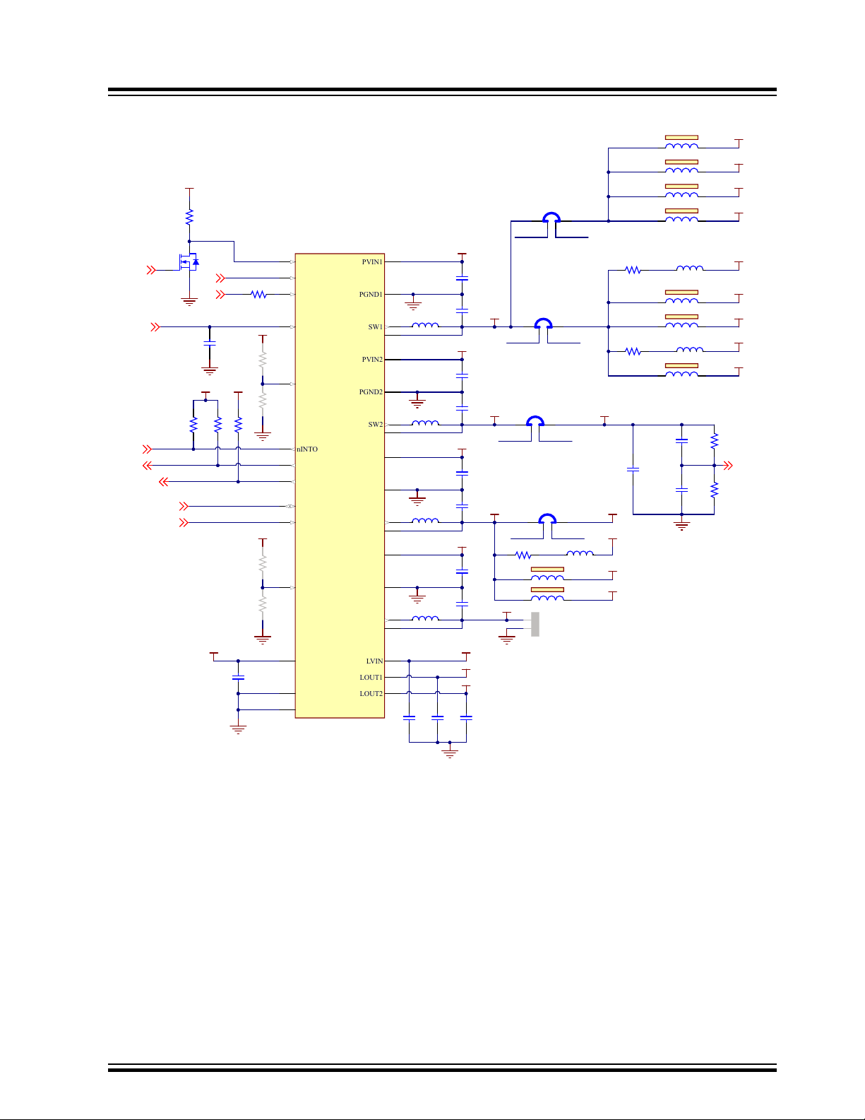
Figure 3-5. Board Power Management
GND
GND
GND
GND
GND
4.7uF
10V
0402
C11
4.7uF
10V
0402
C13
4.7uF
10V
0402
C15
4.7uF
10V
0402
C17
2.2uF
10V
0402
C3
2.2uF
10V
0402
C8
2.2uF
10V
0402
C9
2.2uF
10V
0402
C10
GND
VDD_MAIN_5V
VDD_MAIN_5V
VDD_MAIN_5V
VDD_MAIN_5V
VDD_MAIN_5V
GND
VDD_MAIN_5V
PC28_MCP16502
PC29_MCP16502
0R
0402
R10
DNP
VDD_MAIN_5V
GND
0R
0402
R8
DNP
VDD_MAIN_5V
PC31
PB18
10kR110k
R2
3V3
3V3
WAKE_UP
NRST
180R
FB3
180R
FB4
180R
FB5
180R
FB6
VDDIOP1
VDDIOP0
VDDIOP2
VDDISC
180R
FB7
180R
FB8
180R
FB9
2.2R
R20
2.2R
R21
VDDANA
VDDAUDIOPLL
VDDUTMII
VDDOSC
VDDSDHC
180R
FB1
180R
FB2
2.2R
R19
VDDHSIC
VDDUTMIC
VDDPLLA
1V35
1V25
Vout4
VDD_LED
VDDIODDR
VDDCORE
SENSE1_P
SENSE2_P
SENSE3_P
SENSE4_P
SENSE1_N
SENSE2_N
SENSE3_N
SENSE4_N
SHDN
NSTART
1k
R6
4.7uF
10V
0402
C23
GND
0.1uF
16V
0402
C26
0.1uF
16V
0402
C25
DDR_REF
2.2k
1%
R25
2.2k
1%
R26
LVIN
20
LOUT1
19
LOUT2
21
nINTO
1
PGND2
13
SW2
14
PGND1
12
SW1
11
PVIN1
10
PVIN2
15
EP
33
OUT1
9
OUT2
16
PGND4
29
SW4
30
PGND3
28
SW3
27
PVIN3
26
PVIN4
31
OUT3
25
OUT4
32
nRSTO
2
SGND
3
SVIN
4
SDA
5
SCL
6
nSTRTO
7
PWRHLD
8
LPM
22
HPM
23
nSTRT
24
SELVL1
18
SELV2
17
U2
MCP16502AA
10uH
L6
0.1uF
16V
0402
C2
GND
10uH
L7
10uH
L5
1 2
HDR-2.54 Male 1x2
J3
DNP
GND
0R
0402
R9
DNP
0R
0402
R7
DNP
1 2
3
4
0.01R
12061%
R15
1 2
3
4
0.01R
12061%
R16
1 2
3
4
0.01R
12061%
R17
1 2
3
4
0.01R
12061%
R18
22uF
10V
0805
C12
22uF
10V
0805
C14
22uF
10V
0805
C16
22uF
10V
0805
C18
1.5uH
VLS3012HBX-1R5M
L1
1.5uH
VLS3012HBX-1R5M
L2
1.5uH
VLS3012HBX-1R5M
L3
1.5uH
VLS3012HBX-1R5M
L4
VDDFUSE
PIOBU7
100k
0402
1%
R72
10k
R256
VDDBU
3
1
2
BSS138
Q6
GND
VDD_MAIN_5V
ATSAMA5D2-ICP
Board Components
DS60001592A-page 12
The MCP16502 is a Fast mode Plus device, supporting data transfers at up to 1 Mbit/s as described in the I2C Bus
specification. The MCP16502 is a slave-only device without clock stretching capability. The MCP16502 assumes that
the I2C logic levels on the bus are generated by a device operating from a nominal supply voltage of 3.3V (with ±10%
tolerance). This is typically the I/O voltage generated by Buck1 (VDDIO). Therefore, VIH and VIL are not related to
the SVIN voltage value. The SDA and SCL lines should not be pulled up to the MCP16502 SVIN voltage, but to the
I2C master interface supply voltage (3.3V nominal). The MCP16502 I2C interface is always accessible, even in the
OFF state, as long as the SVIN pin is powered. In the OFF state, the VDDIO voltage from Buck1 is turned off and
therefore the I2C pullup rail must be provided externally.
For more information, refer to the PMIC MCP16502 data sheet.
© 2020 Microchip Technology Inc.
User Guide
Page 13
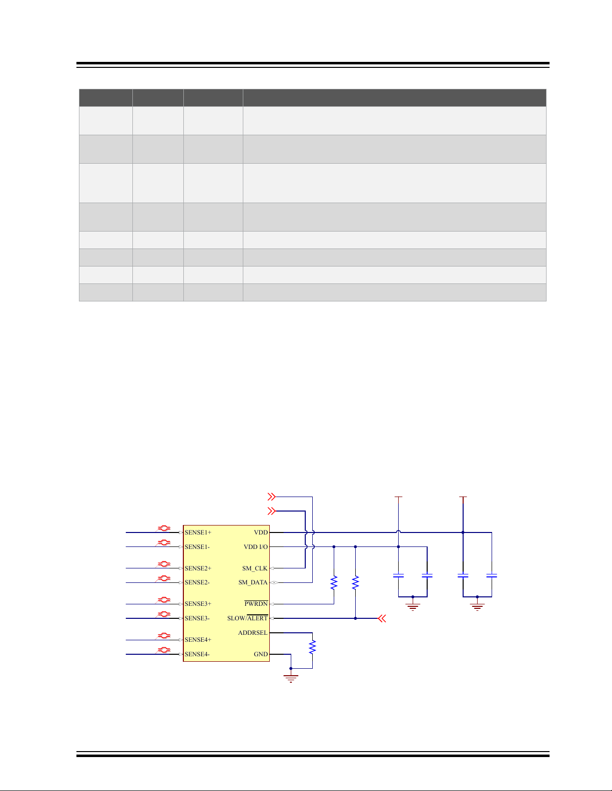
Table 3-4. PMIC Signal Descriptions
2.2uF
10V
0402
C20
0.1uF
16V
0402
C21
2.2uF
10V
0402
C22
0.1uF
16V
0402
C24
GND
GND GND
VDD_MAIN_5V3V3
10k
R23
10k
R24
PB17
PC28_PAC1934
PC29_PAC1934
SENSE2+
A1
SENSE1-
A2
SENSE1+
A3
VDD
A4
SENSE2-
B1
VDD I/O
B2
PWRDN
B3
GND
B4
SENSE3-
C1
ADDRSEL
C2
SLOW/ALERT
C3
SM_CLK
C4
SENSE3+
D1
SENSE4-
D2
SENSE4+
D3
SM_DATA
D4
PAC1934
U3
SENSE1_P
SENSE1_N
SENSE4_P
SENSE4_N
SENSE3_P
SENSE3_N
SENSE2_P
SENSE2_N
0R
0402
R22
PIO Mnemonic Shared PIO Signal Description
ATSAMA5D2-ICP
Board Components
PIOBU7 LPM –
PC31 HPM –
SHDN PWRHLD –
PB_NSTRT nSTRT –
PB18 nINT0 – Active low, open-drain interrupt output
NRST nRSTO NRST Active low, open-drain reset output
PC28 TWD POWER TWI TWI interface serial data
PC29 TWCK POWER TWI TWI interface serial clock
3.2.1.5 Current Measurement
The SAMA5D2-ICP board embeds one PAC1934. The PAC1934 is a four-channel DC power/energy monitor with
accumulator. A 16-bit ADC is used to measure voltages across a current sense resistor, connected by a differential
multiplexer to (+) and (-) inputs for each channel.
Four current sense resistors (10 mΩ) are populated on-board for measuring voltage on power rails:
• 3.3V VDDIOP group (SENSE1_P and SENSE1_N)
• 3.3V VDDOSC, VDDUTMII, VDDANA, VDDAUDIOPLL, VDDSDHC (SENSE2_P and SENSE2_N)
• 1.35V VDDIODDR (SENSE4_P and SENSE4_N)
• 1.25V VDDCORE (SENSE3_P and SENSE3_N)
The PAC1934 communicates with the MPU via a TWI bus.
The figure below shows the current measurement.
Figure 3-6. PAC1934 Current Measurement
Low-Power mode input pin. In combination with PWRHLD and HPM, this
pin defines the power mode status of the MCP16502.
High-Performance mode input pin. In combination with PWRHLD and
LPM, this pin defines the power mode status of the MCP16502.
Power hold input. Typically asserted high by the MPU to maintain power
after the initial startup triggered by nSTRT. PWRHLD will be asserted low
by the MPU to initiate a PMIC shutdown sequence.
Start event input. Drive nSTRT low to initiate a start-up sequence. nSTRT
is internally pulled up.
© 2020 Microchip Technology Inc.
User Guide
DS60001592A-page 13
Page 14

Table 3-5. PAC1934 Signal Descriptions
PIO Mnemonic Shared PIO Signal Description
PC28 PC28_PAC1934 POWER TWI TWI data
PC29 PC29_PAC1934 POWER TWI TWI clock
PB17 INT_PAC1934 – Interrupt
3.2.2 Processor
The Microchip SAMA5D2 Series is a high-performance, power-efficient embedded MPU based on the Arm® Cortex®A5 processor running up to 500 MHz, with support for multiple memories such as DDR2, DDR3, DDR3L, LPDDR1,
LPDDR2, LPDDR3, and QSPI Flash. The devices integrate powerful peripherals for connectivity and user interface
applications, and offer advanced security functions (Arm TrustZone®, tamper detection, secure data storage, etc.), as
well as high-performance cryptoprocessors AES, SHA and TRNG.
For more information about the SAMA5D27 MPU, refer to the SAMA5D2 Series data sheet.
3.2.2.1 Supply Group Configuration
The main regulators provide all power supplies required by the SAMA5D27 device:
• 1.25V VDDCORE, VDDPLLA, VDDUTMIC, VDDHSIC
• 1.35V VDDIODDR
• 2.5V VDDFUSE
• 3.3V VDDIOP0, VDDIOP1, VDDIOP2, VDDISC
• 3.3V VDDOSC, VDDUTMI, VDDANA, VDDAUDIOPLL, VDDSDHC
• 3.3V VDDBU
ATSAMA5D2-ICP
Board Components
© 2020 Microchip Technology Inc.
User Guide
DS60001592A-page 14
Page 15
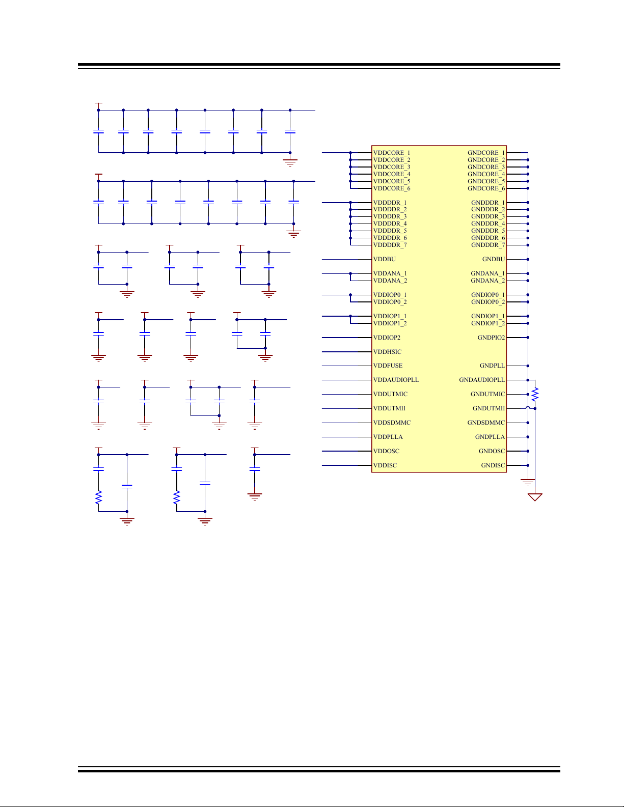
Figure 3-7. Processor Power Lines Supplies
GND
GNDUTMII
VDDCORE
VDDIODDR
VDDBU
VDDIOP0
VDDIOP1
VDDIOP2
VDDANA
VDDHSIC
VDDFUSE
VDDAUDIOPLL
VDDUTMIC
VDDUTMII
VDDSDHC
VDDPLLA
VDDOSC
VDDISC
VDDCORE
10uF
16
0805
C29
10uF
16
0805
C32
GNDVDDIODDR
10uF
16
0805
C30
GND
GND
VDDIOP1
GND
VDDANA
GND
VDDIOP0
GND
VDDBU
GND
VDDIOP2
GND
VDDHSIC
GND
VDDFUSE
GND
VDDUTMIC
VDDCORE
VDDIODDR
VDDBU
VDDANA
VDDIOP0 VDDIOP1
VDDIOP2VDDHSIC VDDFUSE
VDDUTMIC
GND
VDDAUDIOPLL
4.7uF
10V
0402
C57
VDDAUDIOPLL
GND
VDDUTMII
VDDUTMII
GND
VDDPLLA
4.7uF
10V
0402
C69
VDDPLLA
1R
0402
R76
GND
VDDOSC
4.7uF
10V
0402
C71
VDDOSC
1R
0402
R77
GND
VDDISC
VDDISC
GND
VDDSDHC
VDDSDHC
VDDCORE_1
D7
VDDCORE_2
D9
VDDCORE_3
H3
VDDCORE_4
K13
VDDCORE_5
N5
VDDCORE_6
N9
VDDDDR_1
D11
VDDDDR_2
D12
VDDDDR_3
D15
VDDDDR_4
E15
VDDDDR_5
H15
VDDDDR_6
J15
VDDDDR_7
L15
VDDBU
N7
VDDANA_1
K3
VDDANA_2
L5
VDDIOP0_1
E6
VDDIOP0_2
F7
VDDIOP1_1
N13
VDDIOP1_2
R14
VDDIOP2
F10
VDDHSIC
R9
VDDFUSE
M12
VDDAUDIOPLL
T3
VDDUTMIC
P7
VDDUTMII
P8
VDDSDMMC
P11
VDDPLLA
U4
VDDISC
F4
VDDOSC
T7
GNDCORE_1
E7
GNDCORE_2
E9
GNDCORE_3
H4
GNDCORE_4
K12
GNDCORE_5
M5
GNDCORE_6
M9
GNDDDR_1
D14
GNDDDR_2
E11
GNDDDR_3
E12
GNDDDR_4
E14
GNDDDR_5
H14
GNDDDR_6
J14
GNDDDR_7
L14
GNDBU
N6
GNDANA_1
L3
GNDANA_2
K5
GNDIOP0_1
F6
GNDIOP0_2
G7
GNDIOP1_1
M13
GNDPIO2
F9
GNDIOP1_2
P14
GNDPLL
T5
GNDAUDIOPLL
T4
GNDUTMIC
R7
GNDUTMII
P9
GNDSDMMC
R11
GNDPLLA
U5
GNDOSC
T6
GNDISC
G4
ATSAMA5D27C
U4G
0.1uF
16V
0201
C35
0.1uF
16V
0201
C39
0.1uF
16V
0201
C42
0.1uF
16V
0201
C44
0.1uF
16V
0201
C48
0.1uF
16V
0201
C53
0.1uF
16V
0201
C36
0.1uF
16V
0201
C40
0.1uF
16V
0201
C43
0.1uF
16V
0201
C45
0.1uF
16V
0201
C49
0.1uF
16V
0201
C54
0.1uF
16V
0201
C31
0.1uF
16V
0201
C34
0.1uF
16V
0201
C37
0.1uF
16V
0201
C41
0.1uF
16V
0201
C46
0.1uF
16V
0201
C50
0.1uF
16V
0201
C56
0.1uF
16V
0201
C64
0.1uF
16V
0201
C65
0.1uF
16V
0201
C55
0.1uF
16V
0201
C47
0.1uF
16V
0201
C38
0.1uF
16V
0201
C61
0.1uF
16V
0201
C66
4.7uF
10V
0402
C62
0.1uF
16V
0201
C33
0.1uF
16V
0201
C72
0.1uF
16V
0201
C70
0R
0201
R79
0.1uF
16V
0201
C73
ATSAMA5D2-ICP
Board Components
3.2.3 Clock Circuitry
© 2020 Microchip Technology Inc.
The embedded MPU generates the necessary clocks based on two oscillators: one slow clock (SLCK) crystal running
at 32.768 kHz and one main clock oscillator running at 12 MHz. An optional 12 MHz crystal is available as an
alternative to the DSC1001DL5-012.0000 oscillator.
Note: PIOBU0 can be used to disable the 12 MHz main oscillator (Y3).
User Guide
DS60001592A-page 15
Page 16
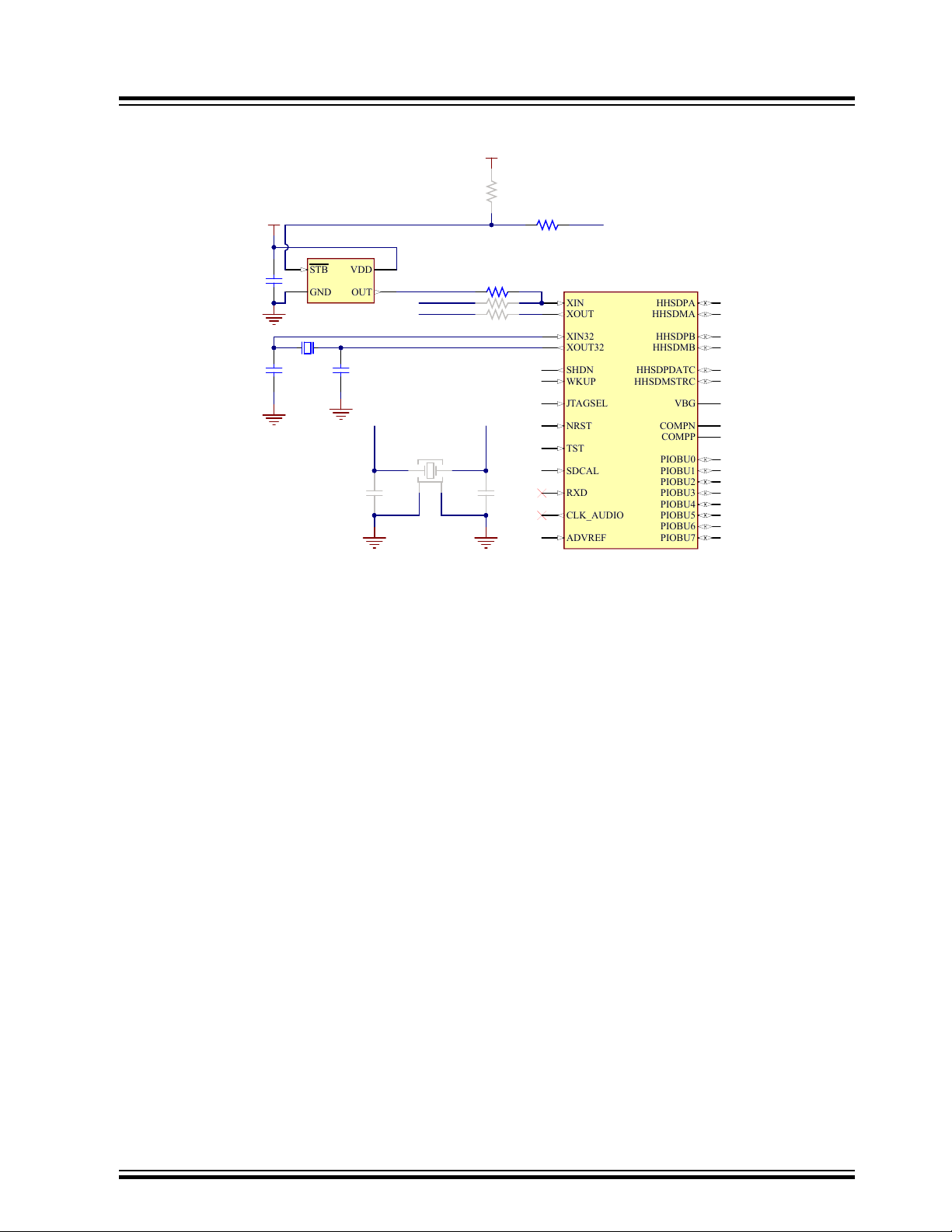
Figure 3-8. MPU Clock Circuitry
0.1uF
16V
0402
C52
GND
3V3
32.768kHz
Y1
GND
GND
Xin_32
Xout_32
GND GND
Xout
Xin
0R
R69
0R
R70
DNP
0R
R71
DNP
Xin
Xout
XIN
U7
XOUT
U6
XIN32
P1
XOUT32
P2
SHDN
R1
WKUP
P4
JTAGSEL
T2
NRST
U2
TST
P3
SDCAL
T10
RXD
N4
CLK_AUDIO
U3
ADVREF
M6
HHSDPA
T8
HHSDMA
R8
HHSDPB
U8
HHSDMB
U9
HHSDPDATC
T9
HHSDMSTRC
U10
VBG
R6
COMPN
U1
COMPP
T1
PIOBU0
R3
PIOBU1
N8
PIOBU2
R2
PIOBU3
R5
PIOBU4
R4
PIOBU5
P5
PIOBU6
P6
PIOBU7
M8
ATSAMA5D27C
U4F
18pF
50V
0402
C299
18pF
50V
0402
C51
12Mhz
1 3
CX3225SB12000H0PSTC1
Y4
DNP
18pF
50V
0402
C67
DNP
18pF
50V
0402
C60
DNP
3V3
0R
0402
R185
0R
0402
R166
DNP
PIOUB0
12.00 MHz
DSC1001DL5-012.0000
STB
1
GND2OUT
3
VDD
4
Y3
ATSAMA5D2-ICP
Board Components
3.2.3.1 Reset Circuitry
The reset sources for the SAMA5D2-ICP board are:
© 2020 Microchip Technology Inc.
• Power-on Reset from the PMIC MCP16502
• Push button reset SW1
• External JTAG or J-Link-OB reset from an in-circuit emulator
User Guide
DS60001592A-page 16
Page 17
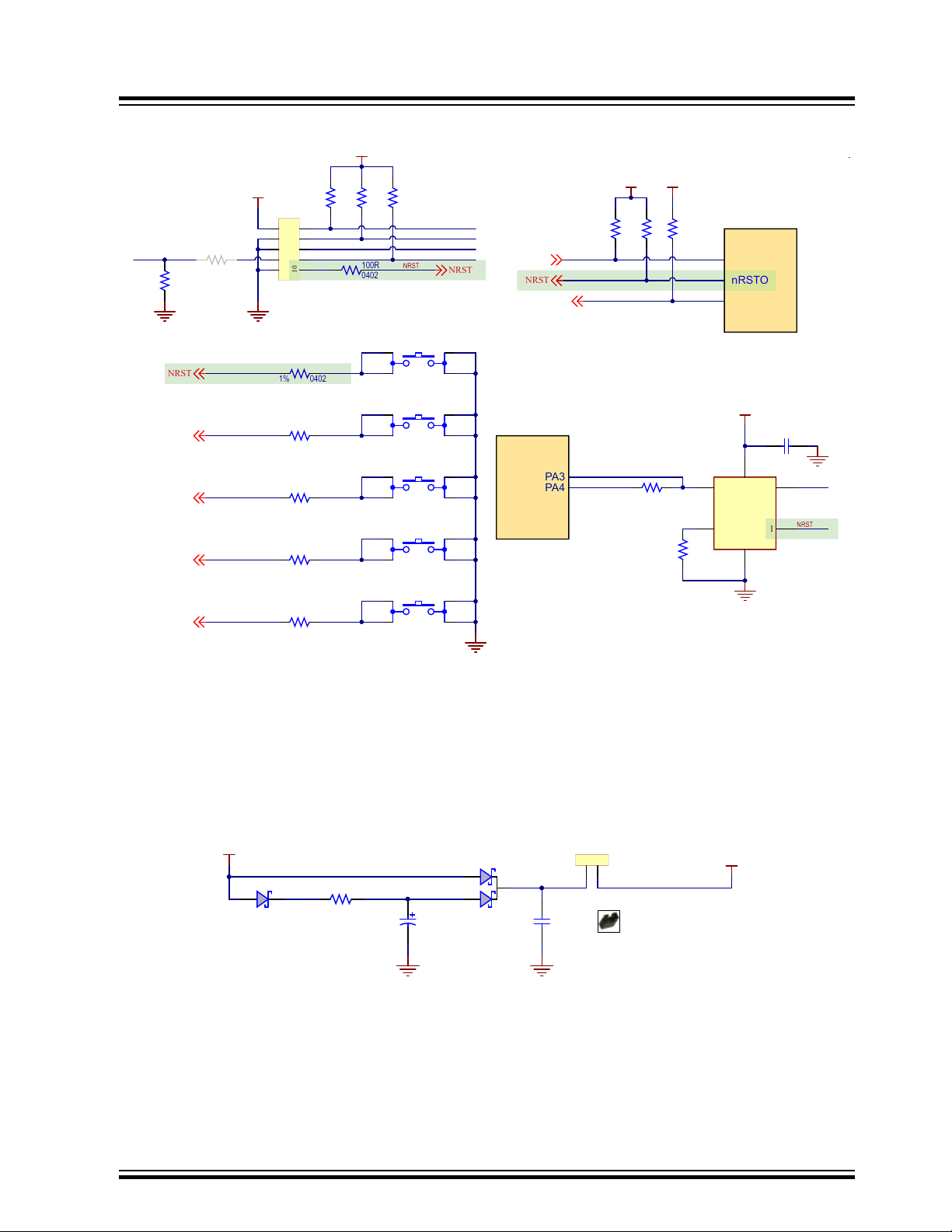
Figure 3-9. Reset Circuitry
1 4
2 3
TACT SPST
SW4
1 4
2 3
TACT SPST
SW1
NRST
1 4
2 3
TACT SPST
SW2
DIS_BOOT
100R
04021%
R252
1 4
2 3
TACT SPST
SW3
GND
100R
04021%
R251
100R
04021%
R250
NSTART
1 4
2 3
TACT SPST
SW5
PIOBU1
PD0
100R
04021%
R254
0R
0603
R255
1
2
3
4
5
6
7
8
9
10
FTSH-105-01-F-DV-K
J18
10k
R208
100R
0402
R210
0R
0603
R209
DNP
100k
0402
R211
100k
0402
R212
100k
0402
R213
NRST
GND GND
3V3
3V3
RTCKIN CON_JTAG_TDI
CON_JTAG_TDO
CON_JTAG_TCK
CON_JTAG_TMS
NRST
1 4
2 3
TACT SPST
SW4
1 4
2 3
TACT SPST
SW1
NRST
1 4
2 3
TACT SPST
SW2
DIS_BOOT
100R
04021%
R252
1 4
2 3
TACT SPST
SW3
GND
100R
04021%
R251
100R
04021%
R250
NSTART
1 4
2 3
TACT SPST
SW5
PIOBU1
PD0
100R
04021%
R254
0R
0603
R255
A
3
B0
4
VCC
1
GND
5
B1
2
S
6
NLAS3157MX3TC
U28
NRST
GND
VDD_3V3_JLINK
150R
R215
1k
R216
TRESIN
TRESOUT PA26_3U
0.1uF
16V0402
C273
GND
PA3
PA4
U27
PB18
10kR110k
R2
3V3
WAKE_UP
NRST
10k
R256
VDDBU
nRSTO
nSTRTO
nINTO
U2
RB160M-60TR
D1
1
2
3
BAT54C
D2
220mF
3.3V
P4.6D4.8H1.66
C5
3V3
VDDBU
0.1uF
16V
0402
C7
GND
100R
08055%
R3
GND
12
HDR-2.54 Male 1x2
J2
Shunt 2.54mm 1x2
JP2
ATSAMA5D2-ICP
Board Components
3.2.3.2 Power Backup Supply
The SAMA5D2-ICP board requires a power source in order to permanently power the backup part of the SAMA5D27
device (refer to the SAMA5D2 Series data sheet). A super capacitor sustains such permanent power to VDDBU
when all system power sources are off.
Figure 3-10. VDDBU Powering Option
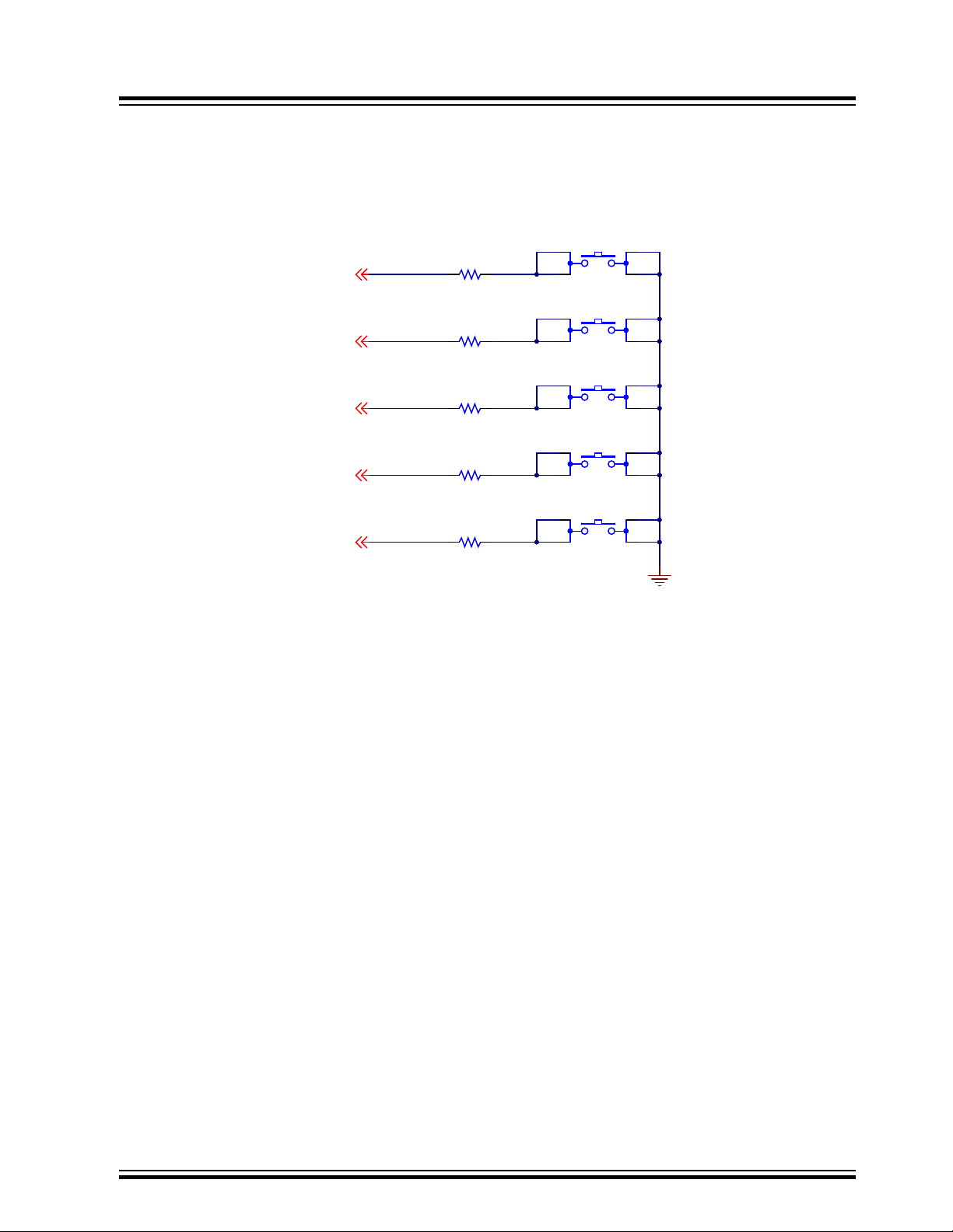
3.2.4 Push Button Switches
The SAMA5D2-ICP features five push buttons:
• One reset push button (SW1). When pressed and released, it causes a general reset of the board
© 2020 Microchip Technology Inc.
User Guide
DS60001592A-page 17
Page 18
1 4
2 3
TACT SPST
SW4
1 4
2 3
TACT SPST
SW1
NRST
1 4
2 3
TACT SPST
SW2
DIS_BOOT
100R
04021%
R252
1 4
2 3
TACT SPST
SW3
GND
100R
04021%
R251
100R
04021%
R250
NSTART
1 4
2 3
TACT SPST
SW5
PIOBU1
PD0
100R
04021%
R254
0R
0603
R255
ATSAMA5D2-ICP
Board Components
• One wake-up push button (SW3) connected to the nSTRT pin of the PMIC, used to signal to the PMIC to initiate
a power-on sequence and to make the processor exit Low-Power mode
• One disable boot push button (SW2) used to invalidate the boot memories (see the section CS Disable)
• Two user push buttons (SW4 and SW5) connected to PIO PD0 and PIOBU1
Figure 3-11. System Push Buttons
3.2.5 Memory
3.2.5.1 Memory Organization
The SAMA5D27 features a DDR/SDR memory interface and an External Bus Interface (EBI) to enable interfacing to
a wide range of external memories and to a wide range of parallel peripherals.
This section describes the memory devices mounted on the SAMA5D2-ICP board:
• Two DDR3L SDRAMs
• One QSPI Flash
• Three serial EEPROMs
Additional memory can be added to the board by:
• Installing an SD or MMC card in the SD/MMC slot
• Using the USB ports
Support is dependent upon driver support in the OS.
3.2.5.2 DDR3L SDRAM
Two DDR3L SDRAMs (W632GU6MB 2 Gbits = 16, 777,216 words x 8 banks x 16 bits) are used as main system
memory, totalling 4 Gbits of SDRAM on the board. The memory bus is 32 bits wide and operates with a frequency of
up to 166 MHz.
© 2020 Microchip Technology Inc.
User Guide
DS60001592A-page 18
Page 19
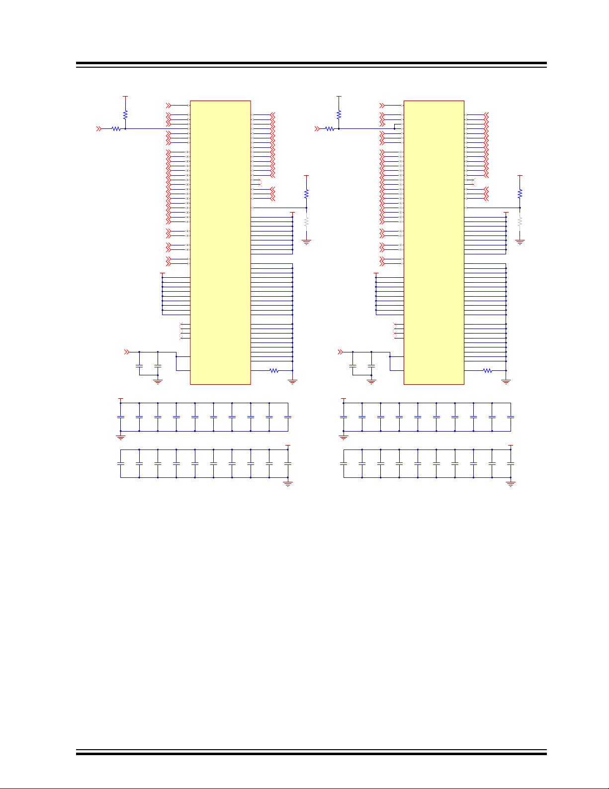
Figure 3-12. DDR3L SDRAM Implementation
DDR_D0
DDR_D1
DDR_D2
DDR_D3
DDR_D4
DDR_D5
DDR_D6
DDR_D7
DDR_D8
DDR_D9
DDR_D10
DDR_D11
DDR_D12
DDR_D13
DDR_D14
DDR_D15
DDR_A0
DDR_A1
DDR_A2
DDR_A3
DDR_A4
DDR_A5
DDR_A6
DDR_A7
DDR_A8
DDR_A9
DDR_A10
DDR_A11
DDR_A12
DDR_A13
DDR_BA0
DDR_BA1
DDR_BA2
DDR_CLK_N
DDR_CKE
DDR_RAS
DDR_CAS
DDR_WE
DDR_CLK_P
DDR_DQS1_P
DDR_DQS1_N
DDR_DQS0_P
DDR_DQS0_N
DDR_DQM1
DDR_DQM0
GND
0R
0402
R86
0R
0402
R87
DNP
GND
CK
J7
CK#
K7
CKE
K9
CS#
L2
RAS#
J3
CAS#
K3
WE#
L3
A0
N3
A1
P7
A2
P3
A3
N2
A4
P8
A5
P2
A6
R8
A7
R2
A8
T8
A9
R3
A10/AP
L7
A11
R7
A12/BC#
N7
A13
T3
NC5
T7
BA0
M2
BA1
N8
BA2
M3
DQL0
E3
DQL1
F7
DQL2
F2
DQL3
F8
DQL4
H3
DQL5
H8
DQL6
G2
DQL7
H7
ODT
K1
VSS1
A9
VSS2
B3
VSS3
E1
VSS4
G8
VSSQ4
D8
VSSQ3
D1
VSSQ2
B9
VSSQ1
B1
VSSQ5
E2
VDDQ1
A1
VDDQ2
A8
VDDQ3
C1
VDDQ4
C9
VDDQ5
D2
VDD1
B2
VDD2
G7
DQSU#
B7
DMU
D3
DML
E7
DQSL#
G3
DQSU
C7
DQSL
F3
DQU0
D7
DQU2
C8
DQU3
C2
DQU6
B8
DQU4
A7
DQU7
A3
DQU5
A2
VDD9
D9
VSSQ6
E8
VDDQ6
E9
VDDQ7
F1
VSSQ7
F9
VSSQ8
G1
VSSQ9
G9
VREFDQ
H1
VDDQ8
H2
VDDQ9
H9
NC1
J1
NC2
J9
VSS5
J2
VSS6
J8
VDD4
K2
VDD5
K8
NC3
L1
ZQ
L8
NC4
L9
VSS7
M1
NC6
M7
VREFCA
M8
VSS8
M9
VDD6
N1
VDD7
N9
VSS9
P1
VSS10
P9
VDD8
R1
VDD3
R9
VSS11
T1
RESET#
T2
VSS12
T9
DQU1
C3
W632GU6MB-12
U6
W632GU6MB
DDR_RESETN
240R
0402 1%
R85
DDR_A0
DDR_A1
DDR_A2
DDR_A3
DDR_A4
DDR_A5
DDR_A6
DDR_A7
DDR_A8
DDR_A9
DDR_A10
DDR_A11
DDR_A12
DDR_A13
DDR_BA0
DDR_BA1
DDR_BA2
DDR_CLK_N
DDR_CKE
DDR_CS
DDR_RAS
DDR_CAS
DDR_WE
DDR_CLK_P
DDR_DQS3_P
DDR_DQS3_N
DDR_DQS2_P
DDR_DQS2_N
DDR_DQM3
DDR_DQM2
0R
0402
R94
0R
0402
R95
DNP
CK
J7
CK#
K7
CKE
K9
CS#
L2
RAS#
J3
CAS#
K3
WE#
L3
A0
N3
A1
P7
A2
P3
A3
N2
A4
P8
A5
P2
A6
R8
A7
R2
A8
T8
A9
R3
A10/AP
L7
A11
R7
A12/BC#
N7
A13
T3
NC5
T7
BA0
M2
BA1
N8
BA2
M3
DQL0
E3
DQL1
F7
DQL2
F2
DQL3
F8
DQL4
H3
DQL5
H8
DQL6
G2
DQL7
H7
ODT
K1
VSS1
A9
VSS2
B3
VSS3
E1
VSS4
G8
VSSQ4
D8
VSSQ3
D1
VSSQ2
B9
VSSQ1
B1
VSSQ5
E2
VDDQ1
A1
VDDQ2
A8
VDDQ3
C1
VDDQ4
C9
VDDQ5
D2
VDD1
B2
VDD2
G7
DQSU#
B7
DMU
D3
DML
E7
DQSL#
G3
DQSU
C7
DQSL
F3
DQU0
D7
DQU2
C8
DQU3
C2
DQU6
B8
DQU4
A7
DQU7
A3
DQU5
A2
VDD9
D9
VSSQ6
E8
VDDQ6
E9
VDDQ7
F1
VSSQ7
F9
VSSQ8
G1
VSSQ9
G9
VREFDQ
H1
VDDQ8
H2
VDDQ9
H9
NC1
J1
NC2
J9
VSS5
J2
VSS6
J8
VDD4
K2
VDD5
K8
NC3
L1
ZQ
L8
NC4
L9
VSS7
M1
NC6
M7
VREFCA
M8
VSS8
M9
VDD6
N1
VDD7
N9
VSS9
P1
VSS10
P9
VDD8
R1
VDD3
R9
VSS11
T1
RESET#
T2
VSS12
T9
DQU1
C3
W632GU6MB-12
U8
W632GU6MB
DDR_RESETN
240R
0402 1%
R92
DDR_REF
DDR_D16
DDR_D17
DDR_D18
DDR_D19
DDR_D20
DDR_D21
DDR_D22
DDR_D23
DDR_D24
DDR_D25
DDR_D26
DDR_D27
DDR_D28
DDR_D29
DDR_D30
DDR_D31
100k
0402
R89
0R
0402
R184
DDR_CS
100k
0402
R178
0R
0402
R4
GND
DDR_REF
0.1uF
16V
0402
C291
GND
0.1uF
16V
0402
C292
0.1uF
16V
0402
C293
0.1uF
16V
0402
C294
VDDIODDRVDDIODDR
VDDIODDR
VDDIODDR
VDDIODDRVDDIODDR
GND
VDDIODDR
0.1uF
16V
0402
C76
2.2uF
10V
0402
C75
0.1uF
16V
0402
C77
0.1uF
16V
0402
C79
0.1uF
16V
0402
C80
0.1uF
16V
0402
C81
0.1uF
16V
0402
C82
0.1uF
16V
0402
C83
0.1uF
16V
0402
C84
0.1uF
16V
0402
C86
GND
0.1uF
16V
0402
C88
2.2uF
10V
0402
C87
0.1uF
16V
0402
C89
0.1uF
16V
0402
C90
0.1uF
16V
0402
C91
0.1uF
16V
0402
C93
0.1uF
16V
0402
C94
0.1uF
16V
0402
C95
0.1uF
16V
0402
C96
0.1uF
16V
0402
C97
GND
VDDIODDRVDDIODDR
0.1uF
16V
0402
C101
2.2uF
10V
0402
C99
0.1uF
16V
0402
C103
0.1uF
16V
0402
C105
0.1uF
16V
0402
C107
0.1uF
16V
0402
C110
0.1uF
16V
0402
C112
0.1uF
16V
0402
C114
0.1uF
16V
0402
C117
0.1uF
16V
0402
C120
GND
VDDIODDR
0.1uF
16V
0402
C102
2.2uF
10V
0402
C100
0.1uF
16V
0402
C104
0.1uF
16V
0402
C106
0.1uF
16V
0402
C108
0.1uF
16V
0402
C111
0.1uF
16V
0402
C113
0.1uF
16V
0402
C115
0.1uF
16V
0402
C118
0.1uF
16V
0402
C121
GND
VDDIODDR
GND
VDDIODDR
ATSAMA5D2-ICP
Board Components
3.2.5.3 DDR_CAL Analog Input
One specific analog input, DDR_CAL, is used to calibrate all DDR I/Os.
© 2020 Microchip Technology Inc.
User Guide
DS60001592A-page 19
Page 20

Figure 3-13. DDR Signals and CAL Analog Input
DDR_D0
DDR_D1
DDR_D2
DDR_D3
DDR_D4
DDR_D5
DDR_D6
DDR_D7
DDR_D8
DDR_D9
DDR_D10
DDR_D11
DDR_D12
DDR_D13
DDR_D14
DDR_D15
DDR_A0
DDR_A1
DDR_A2
DDR_A3
DDR_A4
DDR_A5
DDR_A6
DDR_A7
DDR_A8
DDR_A9
DDR_A10
DDR_A11
DDR_A12
DDR_A13
DDR_BA0
DDR_BA1
DDR_BA2
DDR_CLK_N
DDR_CKE
DDR_CS
DDR_RAS
DDR_CAS
DDR_WE
DDR_CLK_P
DDR_DQS1_P
DDR_DQS1_N
DDR_DQS0_P
DDR_DQS0_N
DDR_DQM1
DDR_DQM0
0.1uF
16V
0402
C28
GND
100k
0402
R65
VDDIODDR
GND
DDR_RESETN
DDR_REF
DDR_D16
DDR_D17
DDR_D18
DDR_D19
DDR_D20
DDR_D21
DDR_D22
DDR_D23
DDR_D24
DDR_D25
DDR_D26
DDR_D27
DDR_D28
DDR_D29
DDR_D30
DDR_D31
DDR_DQM2
DDR_DQM3
DDR_DQS2_P
DDR_DQS2_N
DDR_DQS3_P
DDR_DQS3_N
DDR_A0
F12
DDR_A1
C17
DDR_A2
B17
DDR_A3
B16
DDR_A4
C16
DDR_A5
G14
DDR_A6
F14
DDR_A7
F11
DDR_A8
C14
DDR_A9
D13
DDR_A10
C15
DDR_A11
A16
DDR_A12
A17
DDR_A13
G11
DDR_BA0
H12
DDR_BA1
H13
DDR_BA2
F17
DDR_RAS
F13
DDR_CAS
G12
DDR_CLK
E17
DDR_CLKN
D17
DDR_CKE
F16
DDR_CS
G13
DDR_WE
F15
DDR_CAL
E13
DDR_RESETN
E16
DDR_VREF
D16
DDR_D0
B12
DDR_D1
A12
DDR_D2
C12
DDR_D3
A13
DDR_D4
A14
DDR_D5
C13
DDR_D6
A15
DDR_D7
B15
DDR_D8
G17
DDR_D9
G16
DDR_D10
H17
DDR_D11
K17
DDR_D12
K16
DDR_D13
J13
DDR_D14
K14
DDR_D15
K15
DDR_D16
B8
DDR_D17
B9
DDR_D18
C9
DDR_D19
A9
DDR_D20
A10
DDR_D21
D10
DDR_D22
B11
DDR_D23
A11
DDR_D24
J12
DDR_D25
H10
DDR_D26
J11
DDR_D27
K11
DDR_D28
L13
DDR_D29
L11
DDR_D30
L12
DDR_D31
M17
DDR_DQM0
C11
DDR_DQM1
G15
DDR_DQM2
C8
DDR_DQM3
H11
DDR_DQS0
B13
DDR_DQSN0
B14
DDR_DQS1
J17
DDR_DQSN1
J16
DDR_DQS2
C10
DDR_DQSN2
B10
DDR_DQS3
L17
DDR_DQSN3
L16
DDR_VREF
H16
ATSAMA5D27C
U4E
DDR_CAL
22pF
25V
0201
C27
23.2k
0402
1%
R64
DIFF100
DIFF100
DIFF100
DIFF100
DIFF100
DIFF100
DIFF100
DIFF100
DIFF100
DIFF100
ATSAMA5D2-ICP
Board Components
3.2.6 Additional Memories
3.2.6.1 QSPI Serial Flash
The SAMA5D27 provides one Quad Serial Peripheral Interface (QSPI).
A QSPI is a synchronous serial data link that provides communication with external devices in Master mode.
The QSPI can be used in SPI mode to interface with serial peripherals such as ADCs, DACs, LCD controllers, CAN
controllers and sensors, or in Serial Memory mode to interface with serial Flash memories.
The QSPI allows the system to execute code directly from a serial Flash memory (XIP, or eXecute In Place,
technology) without code shadowing to RAM. The serial Flash memory mapping is seen in the system as other
memories (ROM, SRAM, DRAM, embedded Flash memory, etc.).
With the support of the Quad SPI protocol, the QSPI allows the system to use high-performance serial Flash
memories which are small and inexpensive, instead of larger and more expensive parallel Flash memories.
The figure below illustrates a socket implementation for the QSPI Flash memory.
© 2020 Microchip Technology Inc.
User Guide
DS60001592A-page 20
Page 21

CE
1
SO/SIO1
2
WP/SIO2
3
VSS
4
SI/SIO0
5
SCK
6
HOLD/SIO3
7
VDD
8
SST26VF064B
U7
10k
R84
3V3
10k
R88
3V3
0.1uF
16V0402
C85
GND
GND
PA11_CS PA10_IO3PA8_IO1
PA6_SCK
PA7_IO0
PA9_IO2
10k
R83
3V3
3V3
0.1uF
16V
0402
C78
GND
10k
R80
3V3
GND
DIS_BOOT
NL17SZ126-D
OE
1
A
2
Y
4
GND
3
VCC
5
U5
ATSAMA5D2-ICP
Board Components
Figure 3-14. QSPI Serial Flash
Table 3-6. QSPI Signal Description
PIO Mnemonic Shared PIO Signal Description
PA6 QSPI0_SCK WILC3000 QSPI clock
PA11 QSPI0_CS – Chip select
PA7 QSPI0_IO0 WILC3000 Data0
PA8 QSPI0_IO1 – Data1
PA9 QSPI0_IO2 WILC3000 Data2
PA10 QSPI0_IO3 WILC3000 Data3
3.2.6.1.1 CS Disable
The on-board push button SW2 controls the selection (CS#) of the bootable memory components (QSPI) using a
non-inverting 3-state buffer.
The rule of operation is:
SW2 (DISABLE_BOOT) pressed = booting from QSPI is disabled when a reset occurs
Refer to the SAMA5D2 Series data sheet for more information on standard boot strategies and sequencing.
3.2.6.2 CryptoAuthentication
The ECC608A is a member of the Microchip CryptoAuthentication family of high-security cryptographic devices which
combine world-class hardware-based key storage with hardware cryptographic accelerators to implement various
authentication and encryption protocols.
The ECC608A includes an EEPROM array which can be used for storage of up to 16 keys, certificates,
miscellaneous read/write, read-only or secret data, consumption logging, and security configurations. Access to the
various sections of memory can be restricted in a variety of ways and then the configuration can be locked to prevent
changes.
Table 3-7. ECC608A PIO Signal Descriptions
PIO Mnemonic Shared Signal Description
PD19 TWD1 EEPROM TWI TWI Data
™
PD20 TWCK1 EEPROM TWI TWI Clock
ATECC608A-SSHDA is placed on the same TWI bus as the EEPROM memories and the three mikroBUS
connectors.
© 2020 Microchip Technology Inc.
User Guide
DS60001592A-page 21
Page 22

Figure 3-15. ATECC608A-SSHDA Implementation
GND4SDA
5
SCL
6
VCC
8
ATECC608A-SSHDA
U34
3V3
0.1uF
16V
0402
C241
GND
PD20_ECC608
PD19_ECC608
Figure 3-16. ATECC608A Location
ATSAMA5D2-ICP
Board Components
3.2.6.3 Serial EEPROM with Unique MAC Address
The SAMA5D2-ICP board embeds three Microchip 24AA025E48 I2C serial EEPROMs using the TWI1 interface.
The TWI interface is I2C compatible; it uses only two lines, namely serial data (SDA) and serial clock (SCL).
According to the standard, the TWI clock rate is limited to 400 kHz in Fast mode and 100 kHz in Normal mode, but a
configurable baud rate generator permits the output data rate to be adapted to a wide range of core clock
frequencies. The TWI supports both Master and Slave modes.
The 24AA025E48 provides 2048 bits of serial Electrically-Erasable Programmable Read-Only Memory (EEPROM)
organized as two blocks of 128 x 8-bit memory. In addition, the 24AA025E48 incorporates an easy and inexpensive
method to obtain a globally unique MAC or EUI address (EUI-48™).
The EUI-48 addresses can be assigned as the actual physical address of a system hardware device or node, or it
can be assigned to a software instance. These addresses are factory-programmed by Microchip and guaranteed
unique.
© 2020 Microchip Technology Inc.
User Guide
DS60001592A-page 22
Page 23

CAUTION
10k
R91
0.1uF
16V
0402
C92
3V3
PD20_EEPROM1
PD19_EEPROM1
10k
R97
GND
0.1uF
16V
0402
C98
3V3
3V3
PD20_EEPROM2
PD19_EEPROM2
0.1uF
16V
0402
C109
PD20_EEPROM3
PD19_EEPROM3
10k
R98
A0
5
A1
4
SDA
3
SCL
1
VCC
6
VSS
2
24AA025E48
U9
GND
GND
3V3
A0
5
A1
4
SDA
3
SCL
1
VCC
6
VSS
2
24AA025E48
U10
A0
5
A1
4
SDA
3
SCL
1
VCC
6
VSS
2
24AA025E48
U11
3V3
GND
GND
ATSAMA5D2-ICP
Board Components
One EEPROM device at the address 50h is used as a “software label” to store board information such as
chip type, manufacturer name and production date, using the last two 16-byte blocks in memory. The
information contained in these blocks should not be modified.
Table 3-8. EEPROM TWI Address
Address + Offset + R/W Bit Component
Base (1010) + Offset (001) + R/W EEPROM1(U9)
Base (1010) + Offset (011) + R/W EEPROM2 (U10)
Base (1010) + Offset (000) + R/W EEPROM3 (U11)
Table 3-9. EEPROM PIO Signal Descriptions
PIO Mnemonic Shared Signal Description
PD19 TWD1 EEPROM TWI TWI Data
PD20 TWCK1 EEPROM TWI TWI Clock
The figure below illustrates the implementation of the three EEPROM memories.
Figure 3-17. EEPROM 24AA025E48
3.2.7 Secure Digital Multimedia Card (SDMMC) Interface
The SD (Secure Digital) Card is a non-volatile memory card format used as mass storage memory in mobile devices.
3.2.7.1 Secure Digital Multimedia (SDMMC) Controller
The SAMA5D2-ICP board has one Secure Digital Multimedia Card (SDMMC) interface that supports the MultiMedia
Card (e.MMC) Specification V4.41, the SD Memory Card Specification V3.0, and the SDIO V3.0 specification. It is
compliant with the SD Host Controller Standard V3.0 specification.
The SDMMC0 interface is connected to a standard SD card connector.
3.2.7.2 SD Card Socket
A standard MMC/SD card connector, connected to SDMMC0, is mounted on the bottom side of the board. The
SDMMC0 communication is based on an 8-pin interface (clock, command, four data and power lines). It includes a
card detection switch.
The figure below illustrates the implementation for the SDMMC0 interface.
© 2020 Microchip Technology Inc.
User Guide
DS60001592A-page 23
Page 24

Figure 3-18. SDMMC0 Interface and the Standard SD Socket
123
45
678
68k
1206
5%
R101
10k
R103
10k
R104
10k
R102
0R
0603
R106
0.1uF
16V
0402
C119
10uF
16
0805
C116
GND
3V3
PA5
PA13
PA12
PA1
PA0
PA2
PA3
PA4
DAT3
1
CMD
2
VSS1
3
VDD
4
CLK
5
VSS2
6
DAT0
7
DAT1
8
DAT2
9
CD
10
WP
11
SHIELD
12
SD
J5
ATSAMA5D2-ICP
Board Components
The table below describes the pin assignment of SD/MMC connector J5.
Table 3-10. Standard SD Socket J5 Pin Assignment Signal Description
Function Pin Shared Signal Description
PA5 1 – SDMMC0_DAT3_PA5
PA1 2 – SDMMC0_CMD_PA1
GND 3 – Ground
VCC 4 – VDDSDHC (3v3)
PA0 5 – SDMMC0_CK_PA0
PA13 6 – SDMMC0_CD_PA13 (card detect)
PA2 7 – SDMMC0_DAT0_PA2
PA3 8 – SDMMC0_DAT1_PA3
PA4 9 – SDMMC0_DAT2_PA4
PA13 10 – SDMMC0_CD_PA13
PA12 11 – SDMMC0_WP_PA12
GND 12 – Ground
3.2.8 Communication Interfaces
The SAMA5D2-ICP embeds many communication interfaces and focuses on the following networking features:
• Dual port 10/100 Ethernet switch (Microchip KSZ8563)
• 1-Gbit Ethernet port (Microchip LAN7850)
• EtherCAT dual port (Microchip LAN9252)
• USB hub 4 ports (Microchip USB2534)
• USB device high-speed port
© 2020 Microchip Technology Inc.
User Guide
DS60001592A-page 24
Page 25

• Optional Wi-Fi/BT interface (Microchip WILC3000)
• Dual CAN interface (Microchip MCP2542)
• Serial links
3.2.8.1 Clock Generator
The clock sources of choice for the communication peripherals are MEMS oscillators.
The DSC1001 is a silicon MEMS-based CMOS oscillator offering excellent jitter and stability performance over a wide
range of supply voltages and temperatures.
The DSC6000 family of MEMS oscillators combines industry-leading low power consumption with ultra-small
packages.
Each communication interface uses its own source oscillator:
• One DSC1001DI5-025.0000 (25 MHz) oscillator used for the Ethernet dual switch
• One DSC1001DI5-025.0000 (25 MHz) oscillator used for the Ethernet HSIC interface
• One DSC1001DI5-025.0000 (25 MHz) oscillator used for the EtherCAT interface
• One DSC1001CI5-024.0000 (24 MHz) oscillator used for the USB hub chip
• One DSC6011JI1A-012.0000 oscillator used for the J-Link-OB (12 MHz)
• One DSC1001DL5-012.0000 oscillator used for the SAMA5D27 main clock (12 MHz)
3.2.8.2 10/100 Ethernet Switch
The KSZ8563 is a highly-integrated, IEEE 802.3 compliant networking device that incorporates a layer-2+ managed
Ethernet switch, two 10Base-T/100Base-TX physical layer transceivers (PHYs) and associated MAC units, and one
MAC port with a configurable RGMII/MII/RMII interface for direct connection to a host processor/ controller, another
Ethernet switch, or an Ethernet PHY transceiver. KSZ8563 also implements IEEE 1588v2 Precision Timing Protocol
one-step operation.
Additionally, for monitoring and control purposes, an LED functionality is carried on the RJ45 connectors to indicate
activity, link, and speed status information.
For more information about the Ethernet controller device, refer to the KSZ8563 controller manufacturer's data sheet.
ATSAMA5D2-ICP
Board Components
3.2.8.2.1 External Chip Reset
When the Reset push button switch is pressed, the device places all pins into their default state. An additional PIO
resets the KSZ8563.
The figure below illustrates the implementation of the Ethernet switch interface.
© 2020 Microchip Technology Inc.
User Guide
DS60001592A-page 25
Page 26

Figure 3-19. Ethernet Switch
51R
0603
R148
TX1_P
TX1_N
RX1_P
RX1_N
LED1_1
LED1_0
TX2_P
TX2_N
RX2_P
RX2_N
LED2_1
LED2_0
PD13
PD14
PD5
PD6
PD1
PD11
PD12
PD15
PD16
PD7
PD8
PD9
PD10
PD2
DVDDL
AVDDL
VDDIO
AVDDH
6.04k
0402
R149
GND
PC16
PD3
GND
A
1
B
2
GND
3
Y
4
VCC
5
SN74LVC1G08DBVR
U20
0.1uF
16V0402
C184
GND
3V3
PD4
NRST
1 3
25MHz
Y8
DNP
22pF
50V
0402
C189
DNP
GND GND
Xo1
Xi1
22pF
50V
0402
C183
DNP
0R
R147
DNP
0R
R146
DNP
Xo1
Xi1
VDDIO
1
2
3
HDR-2.54 Male 1x3
J27
DNP
GND
1k
R136
4.7k
0402
R266
4.7k
0402
R157
4.7k
0402
R156
4.7k
0402
R155
4.7k
0402
R259
4.7k
0402
R267
GND
10k
0402
1%
R153
10k
0402
1%
R177
i
Ethernet_SIG
PB28
PB29
PB30
PC0
3V3
10k
0402
1%
R263
10k
0402
1%
R264
3V3
3V3
GND
10k
0402
1%
R265
3V3
STB
1
GND2OUT
3
VDD
4
DSC1001DI5-025.0000
Y7
3V3
GND
0.1uF
16V
0402
C182
3V3
GND
RX2P
12
TX2M
10
TX2P
9
LED1_1
56
LED1_0
55
RX1M
6
RX1P
5
TX1M
3
TX1P
2
POWER
RX2M
13
LED2_0
43
LED2_1
44
ETH PORT1
ETH PORT2
XI
62
XO
61
INTRP_N
46
PME_N
45
ISET
64
GPIO_1
40
GPIO_2
41
RXD0
21
GPIO
OTHER SIGNALS
OSC
AVDDH1AVDDH8AVDDH
15
AVDDL60AVDDL7AVDDL11AVDDL
14
DVDDL31DVDDL34DVDDL42DVDDL54DVDDL
59
VDDIO23VDDIO36VDDIO38VDDIO51VDDIO
57
RXD1
20
RXD2
19
RXD3
18
TXD0
29
TXD1
28
TXD2
27
TXD3
26
TX_ER
33
SDO
48
SCS_N
52
AVDDL
4
GND
16
DVDDL
17
GND35GND37GND39GND50GND58GND
63
RX_CLK / REFCLKO
22
RX_DV / CRS_DV / RX_CTL
24
RX_ER
25
TX_CLK / REFCLKI
30
TX_EN / TX_CTL
32
SCL / MDC
53
RESET_N
47
SDI / SDA / MDIO
49
P_GND
65
KSZ8563RNX
U21
GND
ATSAMA5D2-ICP
Board Components
Table 3-11. 10/100 Mb/s Ethernet Switch Signal Descriptions
PIO Mnemonic Shared Signal Description
PD9 ETH_GTXCK – Transmit clock
PD10 ETH_GTXEN – Transmit enable
PD2 ETH_GTXER – Transmit error
PD15 ETH_GTX0 – Transmit data 0
PD16 ETH_GTX1 – Transmit data 1
PD7 ETH_GTX2 – Transmit data 2
PD8 ETH_GTX3 – Transmit data 3
PD1 ETH_GRXCK – Receive clock
PD11 ETH_GRXDV – Receive data valid
PD12 ETH_GRXER – Receive error
PD13 ETH_GRX0 – Receive data 0
PD14 ETH_GRX1 – Receive data 1
PD5 ETH_GRX2 – Receive data 2
PD6 ETH_GRX3 – Receive data 3
PB30 ETH_GMDC – Management data clock
© 2020 Microchip Technology Inc.
User Guide
DS60001592A-page 26
Page 27

TX1_N
RX1_N
RX1_P
330R
0603
R158
LED1_1
PORT 1
0.1uF
16V 0402
C214
3V3
330R
0603
R159
LED1_0
TX1_P
0.1uF
16V 0402
C213
GND
GND ETH
DIFF100
DIFF100
DIFF100
DIFF100
TD-
2
TCT
4
TD+
1
RD-
6
RCT
5
RD+
3
4X 75R
1nF,2kV
1 TX+
2 TX3 RX+
6 RX4
5
7
8
SHLD
8
NC
7
Right
12
11
9
10
Left
SHLD
13
SHLD
14
RJ45
J00-0045NL
J11
TX2_N
TX2_P
RX2_N
RX2_P
PORT 2
LED2_1
LED2_0
330R
0603
R160
0.1uF
16V 0402
C216
3V3
330R
0603
R161
0.1uF
16V 0402
C215
GND
GND ETH
DIFF100
DIFF100
DIFF100
DIFF100
TD-
2
TCT
4
TD+
1
RD-
6
RCT
5
RD+
3
4X 75R
1nF,2kV
1 TX+
2 TX3 RX+
6 RX4
5
7
8
SHLD
8
NC
7
Right
12
11
9
10
Left
SHLD
13
SHLD
14
RJ45
J00-0045NL
J12
ATSAMA5D2-ICP
Board Components
...........continued
PIO Mnemonic Shared Signal Description
PB28 ETH_GMDIO – Management data in/out
PD3 ETH_GTX_INT – Interrupt (open drain)
PD4 ETH_RST – PIO reset
PC16 ETH_PME_N – Power management event
Figure 3-20. Ethernet Switch Connectors J11 and J12
© 2020 Microchip Technology Inc.
User Guide
DS60001592A-page 27
Page 28

Figure 3-21. Ethernet Switch RJ45 Connectors J11 and J12 Location
ATSAMA5D2-ICP
Board Components
The table below describes the pin assignment of Ethernet connectors J11 and J12.
Table 3-12. Ethernet Switch RJ45 Connectors J11 and J12 Pin Assignment Signal Descriptions
Pin No Mnemonic Signal Description
1 TX+ Transmit
2 TX- Transmit
3 RX+ Receive
4 Decoupling capacitor –
5 Decoupling capacitor –
6 RX- Receive
7 NC –
8 EARTH / GND Common ground
9 ACT LED LED activity
10 ACT LED LED activity
11 LINK LED LED link connection
12 LINK LED LED link connection
13 EARTH / GND Common ground
14 EARTH / GND Common ground
© 2020 Microchip Technology Inc.
User Guide
DS60001592A-page 28
Page 29

3.2.8.3 1-Gbit Ethernet HSIC
The Microchip LAN7850 is a USB 2.0 Gigabit Ethernet Controller with HSIC interface. The LAN7850 supports
10Base/100Base-TC/1000Base-T Ethernet (full duplex support), is configured for operation through internal default
settings and supports custom configuration through the external 4-Kbit EEPROM device or interval one-time
programmable (OTP) memory.
The LAN7850 contains an integrated 10/100/1000 Ethernet MAC and PHY, Filtering Engine, USB PHY (with HSIC
interface), high-speed USB 2.0 device controller, TAP controller, EEPROM controller, and a FIFO controller with
internal packet buffering.
The Ethernet controller supports auto-negotiation, auto-polarity correction and HP Auto-MDIX, and is compliant with
the IEEE 802.3, IEEE 802.3u, IEEE 802.3ab, and 802.3az (Energy Efficient Ethernet) standards. ARP and NS offload
are also supported.
An internal EEPROM controller exists to load various USB and Ethernet configuration parameters. For EEPROM-less
applications, the LAN7850 provides 1 Kbyte of OTP memory that can be used to preload this same configuration data
before enumeration.
3.2.8.3.1 External EEPROM / Internal OTP
At power-up, the LAN7850 searches for an external EEPROM. If an external EEPROM (93AA66A) is detected, the
LAN7850 configuration is loaded from it. If no EEPROM is found, the device checks the OTP. If there is no OTP, the
device uses default CSR settings. The EEPROM stores the default values for the USB descriptors and the MAC
address.
3.2.8.3.2 Enable Link Status LEDs
When configured with the default internal register settings, the Ethernet link status LEDs are not enabled. To enable
those LEDs, enable the EEPROM.
Each LED is detailed below:
• Link1000: yellow LED (RJ45 J10) is ON with a valid 1000 Mbps link.
• Link100: green LED (RJ45 J10) is ON with a valid 100 Mbps link.
• Link/Act: RGB LED (LD5) is ON and green with network activity.
• Duplex/Collision: RGB LED (LD5) is ON and red in Full Duplex mode. LED is OFF in Half-Duplex mode. LED
blinks red during collision.
• Suspend: RGB LED (LD5) is ON and blue in Suspend mode.
ATSAMA5D2-ICP
Board Components
3.2.8.3.3 External Chip Reset
When the Reset push button switch is pressed, the device places all pins into their default state and the entire
contents of the EEPROM or OTP are reloaded. An additional PIO (PC2) allows the LAN7850 to be reset by software.
The figure below illustrates the implementation of the Ethernet HSIC interface.
© 2020 Microchip Technology Inc.
User Guide
DS60001592A-page 29
Page 30

Figure 3-22. Ethernet HSIC Interface
REF_REXT
REF_FILT
TR0_P
TR0_N
TR1_P
TR1_N
TR2_P
TR2_N
TR3_P
TR3_N
1uF
0603
C159
2k
0402
1%
R139
GND
LED1
LED0
1k
R137
1k
R152
2.2k
R138
3V3
HSIC_STROBE
35
USB_DP
36
USB_DM
37
HSIC_DATA
38
USB_RBIAS
43
VBUS_DET
27
XI
46
X0
47
TEST
40
EECS/GPIO1
21
EEDI/GPIO2
22
EEDO/GPIO3
23
EECLK/GPIO4
24
TDI
14
TDO
15
TCK/GPIO0
16
TMS
17
TR0P
1
TR0N
2
TR1P
4
TR1N
5
TR2P
7
TR2N
8
TR3P
10
TR3N
11
REF_REXT
55
REF_FILT
56
RESET_N/PME_CLEAR
41
PME_N
39
LED1/GPIO9
49
LED2/GPIO10
50
LED3/GPIO11
51
SUSPEND_N/GPIO5
28
HSIC_SEL
30
CONNECT/GPIO6
29
LED0/GPIO7
31
PME_MODE/GPIO8
32
LAN7850T
U19A
LAN7850 QFN-56
LED2
LED3
LED3
LED2
SUSPEND_N
SUSPEND_N
51R
06031%
R135
12k
R133
GND
10k
R131
10k
R132
3V3
PC1
HSIC_DATA
HSIC_STROBE
GND
A
1
B
2
GND
3
Y
4
VCC
5
SN74LVC1G08DBVR
U18
0.1uF
16V0402
C156
GND
3V3PC2
NRST
PC22
PC24
PC23
GND ETH3GND
68R
0603
R145
LED1
68R
0603
R144
LED0
3V3
3V3
10k
R134
10k
R150
10k
R151
3V3
180R
FB21
GND ETH3GND
CS
1
CLK
2
DI
3
DO
4
VSS
5
ORG
6
NC
7
VCC
8
93AA66A
U33
0.1uF
16V
0402
C167
GND
3V3
3V3
STB
1
GND2OUT
3
VDD
4
DSC1001DI5-025.0000
Y6
GND
0.1uF
16V
0402
C155
3V3
GND
10k
R268
DNP
GND
3
1
2
5
6
4
J8
J7
J5
J4
0
J6
J3
J2
J1
1nF,2kV
4X 75R
0.1uF
0.1uF
0.1uF
0.1uF
Right
Left
7
8
9
10
11
12
13
14
CON MODULAR JACK RJ45 10/100/1000 MAGNETICS
J10
GREEN
BLUE
2
1
RED
4
3
RED, GREEN, BLUE
LD5
LED_RGB_CLV1A
i
HSIC_SIG
DIFF100
DIFF100
DIFF100
DIFF100
DIFF100
DIFF100
DIFF100
DIFF100
ATSAMA5D2-ICP
Board Components
Table 3-13. Ethernet HSIC Signal Description
PIO Mnemonic Shared Signal Description
– HSIC_STROBE – Bidirectional data strobe signal
– HSIC_DATA –
PC22 VBUS_DETECT – Sets the state of the upstream bus power
PC23 PME_N –
PC24 PME_MODE –
© 2020 Microchip Technology Inc.
Bidirectional Double Data Rate (DDR) data signal that is synchronous to the
strobe signal
effect
Indicates Power Management Event when the PME mode of operation is in
Serves as the Power Management Event mode selection input when the PME
mode of operation is in effect
User Guide
DS60001592A-page 30
Page 31

Figure 3-23. Ethernet HSIC RJ45 Connector J10 Location
ATSAMA5D2-ICP
Board Components
3.2.8.4 EtherCAT
The LAN9252 is a 2-port EtherCAT Slave Controller (ESC) with dual integrated Ethernet PHYs. Each PHY contains a
full-duplex transceiver and supports 100 Mbps (100Base-TX) operation.
PORT0 of LAN9252 is connected to the host processor through the PIOs in HBI Indexed mode. The HBI supports
8/16-bit operation with Big, Little, and Mixed Endian operations. Two process data RAM FIFOs interface the HBI to
the EtherCAT slave controller and facilitate the transferring of process data information between the host CPU and
the EtherCAT slave. A configurable host interrupt pin allows the device to inform the host CPU of any internal
interrupts.
Several PIOs are shared with the Wi-Fi/BT WILC3000 interface. When the WILC3000 interface is enabled, the
LAN9252 (NCS1 PC6) is disabled via the WILC3K_CE PC15 signal.
The LAN9252 is connected to two RJ45 Ethernet jacks with integrated magnetics for 100Base-TX connectivity.
Additionally, for monitoring and control purposes, LED functionality is carried on the RJ45 connectors to indicate
activity and link status information.
For more information about the Ethernet controller device, refer to the Microchip LAN9252 controller data sheet.
3.2.8.4.1 External Chip Reset
When the Reset push button switch is pressed, the device places all pins into their default state. An additional PIO
(PB16) allows the LAN9252 to be reset by software.
The figure below illustrates the implementation of the EtherCAT interface.
© 2020 Microchip Technology Inc.
User Guide
DS60001592A-page 31
Page 32

Figure 3-24. EtherCAT Interface
0.1uF
16V
0402
C231
1uF
16V
0603
C226
GND
0.1uF
16V
0402
C218
3V3
0.1uF
16V
0402
C232
1uF
16V
0603
C227
GND
VDD33TXRX1
VDD33TXRX2
VDD33BIAS
VDD33BIAS
0.1uF
16V
0402
C234
GND
VDD12TX
GND
0.1uF
16V
0402
C219
0.1uF
16V
0402
C220
0.1uF
16V
0402
C223
0.1uF
16V
0402
C225
0.1uF
16V
0402
C228
0.1uF
16V
0402
C230
GND
3V3
0.1uF
16V
0402
C237
0.1uF
16V
0402
C238
0.1uF
16V
0402
C239
GND
0.1uF
16V
0402
C233
3V3
GND
12.1k
04021%
R174
VDDCR
4.7k
0402
R176
4.7k
0402
R179
0.1uF
16V
0402
C235
GND
3V3
GND
3V3
GND
51R
06031%
R168
10k 0402
R180
GND
10k 0402
R181
GND
txa_n
txa_p
rxa_n
rxa_p
txb_n
txb_p
rxb_n
GPOI2
PA22_D0
PA23
PA24
PA25
PA26
PA27
PA28_D6
PA29
PB3
PB4
PB5
PB6
PB7
PB8
PB9
PB10
PB12
PB13
PB14
PB15
FX_Los_Strap
FX_Mode_Strap
220R
FB22
220R
FB23
220R
FB24
220R
FB25
A0
1
SDA
5
A2
3
A1
2
WP
7
VSS
4
SCL
6
VCC
8
24FC512
U25
I2C EEPROM
PB16
PB11
10k
R171
3V3
GND
A
1
B
2
GND
3
Y
4
VCC
5
SN74LVC1G08DBVR
U22
0.1uF
16V0402
C217
3V3
NRST
0R
R169
DNP
0R
R170
DNP
1 3
25MHz
Y10
DNP
22pF
50V
0402
C229
DNP
GND GND
22pF
50V
0402
C222
DNP
3V3
GND
GND
3V3
EESCL
EESDA
EESCL
EESDA
GPIO1
GPIO0
rxb_p
0R
R165
VDD33TXRX2
VDD33TXRX1
VDDCR
0.1uF
16V
0402
C287
1uF
16V
0603
C286
GND
1uF
16V
0603
C236
0.1uF
16V
0402
C288
0.1uF
16V
0402
C289
GND
VDD12TX
i
EtherCAT_SIG
3V3
GPOI2
10k
R172
GREEN
D91kR173
0.1uF
16V 0402
C224
1
2
3
HDR-1.27 Male 1x3
J4
DNP
GND
J4 is used for one
time programming of
the EEPROM
STB
1
GND2OUT
3
VDD
4
DSC1001DI5-025.0000
Y9
GND
GND
3V3
VDD33
5
VDD33BIAS
58
REG_EN
7
VDD33TXRX264VDD33TXRX1
51
ePad
65
VDDIO114VDDIO220VDDIO332VDDIO437VDDIO5
47
VDDCR16VDDCR224VDDCR3
38
VDD12TX156VDD12TX2
59
POWER
PORT0
PORT1
I2C
RBIAS
57
TESTMODE
41
D0/AD0/WD_STATE/SI/SIO0
17
D1/AD1/EOF/SO/SIO1
13
D2/AD2/SOF/SIO2
12
D3/AD3/WD_TRIG/SIO3
35
D4/AD4/DIGIO3/GPI3/GPO3/MII_LINK
49
D5/AD5/OUTVALID/SCS#
50
D6/AD6/DIGIO0/GPI0/GPO0/MII_RXCLK
36
D7/AD7/DIGIO1/GPI1/GPO1/MII_MDC
39
D8/AD8/DIGIO2/GPI2/GPO2/MII_MDIO
40
D9/AD9/LATCH_IN/SCK
19
D10/AD10/DIGIO4/GPI4/GPO4/MII_TXEN
23
D11/AD11/DIGIO5/GPI5/GPO5/MII_TXD0
22
D12/AD12/DIGIO6/GPI6/GPO6/MII_TXD1
21
D13/AD13/DIGIO7/GPI7/GPO7/MII_TXD2/TX_SHIFT0
16
D14/AD14/DIGIO8/GPI8/GPO8/MII_TXD3/TX_SHIFT1
15
A0/D15/AD15/DIGIO9/GPI9/GPO9/MII_RXER
33
A1/ALELO/OE_EXT/MII_CLK25
25
A3/DIGIO11/GPI11/GPO11/MII_RXDV
26
A4/DIGIO12/GPI12/GPO12/MII_RXD0
27
RD/RD_WR/DIGIO15/GPI15/GPO15/MII_RXD3
31
WR/ENB/DIGIO14/GPI14/GPO14/MII_RXD2
30
CS/DIGIO13/GPI13/GPO13/MII_RXD1
28
GPIO
OTHER SIGNALS
OSC
RST_n
11
IRQ
44
LINKACTLED0/TDO/CHIP_MODE0
48
LINKACTLED1/TDI/CHIP_MODE1
46
EESCL/TCK
43
EESDA/TMS
42
FXLOSEN
8
FXSDB/FXLOSB/FXSDENB
10
RXPB
60
RXNB
61
TXPB
62
TXNB
63
FXSDA/FXLOSA/FXSDENA
9
TXNA
52
TXPA
53
RXNA
54
RXPA
55
OSCI
1
OSCO
2
OSCVDD12
3
OSCVSS
4
SYNC1/LATCH1
18
SYNC0/LATCH0
34
RUNLED/E2PSIZE
45
A2/ALEHI/DIGIO10/GPI10/GPO10/LINKACTLED2/MII_LINKPOL
29
LAN9252I/ML
U24
DIFF100
DIFF100
DIFF100
DIFF100
DIFF100
DIFF100
DIFF100
DIFF100
10k
R175
GND
Loss Of signal mode is enabled
FX_Los_Strap
for both PHY A and PHY B
GND
PB2
PA30
PC6_NCS1
PC6
10k
R167
3V3
3V3
0.1uF
16V
0402
C221
GND
GND
PC6_NCS1
PC15 OE
1
A
2
Y
4
GND
3
VCC
5
NL17SZ125-D
U23
ATSAMA5D2-ICP
Board Components
The table below shows the signal assignment on the HBI interface between SAMA5D27 and LAN9252.
Table 3-14. EBI Signal Description
PIO Mnemonic Shared Signal Description
PA22 D0 WILC3000 Data
PA23 D1 – Data
PA24 D2 – Data
© 2020 Microchip Technology Inc.
User Guide
DS60001592A-page 32
Page 33

ATSAMA5D2-ICP
Board Components
...........continued
PIO Mnemonic Shared Signal Description
PA25 D3 – Data
PA26 D4 – Data
PA27 D5 – Data
PA28 D6 WILC3000 Data
PA29 D7 – Data
PB3 D8 – Data
PB4 D9 – Data
PB5 D10 – Data
PB6 D11 – Data
PB7 D12 – Data
PB8 D13 – Data
PB9 D14 – Data
PB10 A0/D15 – Data
PB12 A1 – Address
PB13 A2 – Address
PB14 A3 – Address
PB15 A4 – Address
PB2 RD – Read
PA30 WR – Write
PC6 CS – Chip select
PB11 IRQ – Interrupt
PB16 RESET – Reset chip
The figure below depicts the connection between LAN9252 and the two EtherCAT connectors.
© 2020 Microchip Technology Inc.
User Guide
DS60001592A-page 33
Page 34

49.9R
0402
0.1%
R182
49.9R
0402
0.1%
R188
49.9R
0402
0.1%
R190
49.9R
0402
0.1%
R194
0.022uF
50V
0603
C248
10pF
50V
0402
C240
GNDGND
VDD33TXRX1
10pF
50V
0402
C242
10pF
50V
0402
C244
10pF
50V
0402
C246
PORT A
49.9R
0402
0.1%
R193
49.9R
0402
0.1%
R195
49.9R
0402
0.1%
R197
49.9R
0402
0.1%
R260
0.022uF
50V
0603
C181
10pF
50V
0402
C162
GNDGND
VDD33TXRX2
10pF
50V
0402
C164
10pF
50V
0402
C165
10pF
50V
0402
C166
PORT B
txa1_p
txa1_n
rxa1_p
rxa1_n
txb1_p
txb1_n
rxb1_p
rxb1_n
1k
R82
GPIO1
GPIO0
1k
R164
Earth ETH1
Green = Link/ACT
Yellow = Speed NA for EtherCAT
txa_n
txa_p
rxa_n
rxa_p
0R
R140
0R
R141
0R
R142
0R
R143
D19
GND
GND
D20
B0520WS
D11
B0520WS
D12
B0520WS
D13
B0520WS
D14
Earth ETH1
D21
0R
R183
0R
R189
0R
R191
0R
R192
GND
D22
GND
txb_p
txb_n
rxb_p
rxb_n
B0520WS
D15
B0520WS
D17
B0520WS
D16
B0520WS
D18
GND
10k
0402
R261
GND
GND
10k
0402
R262
GND
TD-
2
TCT
4
TD+
1
RD-
6
RCT
5
RD+
3
4X 75R
1nF,2kV
1 TX+
2 TX3 RX+
6 RX4
5
7
8
SHLD
8
NC
7
Right
12
11
9
10
Left
SHLD
13
SHLD
14
RJ45
J00-0045NL
J13
TD-
2
TCT
4
TD+
1
RD-
6
RCT
5
RD+
3
4X 75R
1nF,2kV
1 TX+
2 TX3 RX+
6 RX4
5
7
8
SHLD
8
NC
7
Right
12
11
9
10
Left
SHLD
13
SHLD
14
RJ45
J00-0045NL
J14
DIFF100
DIFF100
DIFF100
DIFF100
DIFF100
DIFF100
DIFF100
DIFF100
Figure 3-25. EtherCAT Connectors J13 and J14
ATSAMA5D2-ICP
Board Components
The position of the two connectors is shown in the picture below
© 2020 Microchip Technology Inc.
User Guide
DS60001592A-page 34
Page 35

Figure 3-26. RJ45 Connectors J13 and J14 Location
ATSAMA5D2-ICP
Board Components
3.2.8.5 USB Host/Device Ports
The USB (Universal Serial Bus) is a hot-pluggable general-purpose high-speed I/O standard for computer
peripherals. The standard defines connector types, cabling, and communication protocols for interconnecting a wide
variety of electronic devices. The USB 2.0 Specification defines data transfer rates as high as 480 Mbps (also known
as High-speed USB). A USB host bus connector uses four pins: a power supply pin (5V), a differential pair (D+ and
D- pins) and a ground pin.
The SAMA5D2-ICP board features three USB communication ports, designated USB-A to USB-C:
• USB-A interface connected to a standard Micro-AB connector with a VBUS detection function
• USB-B (host port B high- and full-speed interface) connected to a USB2534 hub, with four ports connected to
two stacked USB type A connectors
• USB-C high-speed host port with an HSIC interface, connected to Ethernet Gigabit interface LAN7850
USB IO lines are not controlled by any PIO controller. The embedded USB high-speed physical transceivers are
controlled by the USB host controller.
3.2.8.6 USB-A Interface
The USB Host Port controller is fully compliant with the Enhanced HCI specification. It handles the Open HCI (Open
Host Controller Interface) protocol as well as the Enhanced HCI (Enhanced Host Controller Interface) protocol. The
USB Host Port User interface can be found in the Enhanced HCI Rev 1.0 Specification.
© 2020 Microchip Technology Inc.
User Guide
DS60001592A-page 35
Page 36

Figure 3-27. Micro-AB Type USB Connector J9 Location
Earth USBGND
HHSA_p
HHSA_n
100k
R130
200k
0402
1%
R129
22pF
50V
0402
C152
PD23
ID
4
VBUS
1
GND
5
D-
2
D+
3
0
0475890001
J9
USB MicroAB
GND
ATSAMA5D2-ICP
Board Components
The figure below shows the USB implementation on the USB-A port terminated on a Micro-AB type USB connector.
Figure 3-28. USB-A and VBUS Detection
The table below describes the pin assignment of the USB-B downstream connectors.
Table 3-15. USB-A Connector Signal Descriptions
Pin No Mnemonic Signal Description
1 VBUS 5V power
2 DM Data minus
3 DP Data plus
4 NC Not connected
5 GND Common ground
3.2.8.6.1 USB-A VBUS Detection
The USB-A port (J9) features a VBUS (+5V) insert detection function through ladder-type resistors R129 and R130.
© 2020 Microchip Technology Inc.
User Guide
DS60001592A-page 36
Page 37

Table 3-16. USB-A PIO Signal Descriptions
USBD1_n
USBD2_n
USBD3_n
USBD4_n
USBD1_p
USBD2_p
USBD3_p
USBD4_p
CMD_PWR1
CMD_PWR2
CMD_PWR3
CMD_PWR4
OCS#1
OCS#2
OCS#3
OCS#4
100k
R120
100k
R121
100k
R122
100k
R123
GND
GND
3V3
A
1
B
2
GND
3
Y
4
VCC
5
SN74LVC1G08DBVR
U12
0.1uF
16V0402
C123
GND
3V3
10k
R111
DNP
GND
0.1uF
16V
0402
C135
10k
R113
GND
3V3
0.1uF
16V
0402
C128
0.1uF
16V
0402
C134
0.1uF
16V
0402
C133
0.1uF
16V
0402
C126
0.1uF
16V
0402
C127
3V3
GND
GND
PC17
51R
0603
1%
R108
SWAP_USBDN1_DM/PRT_DIS_M1
1
SWAP_USBDN1_DP/PRT_DIS_P1
2
USBDN2_DM/PRT_DIS_M2
3
USBDN2_DP/PRT_DIS_P2
4
NC1
5
USBDN3_DM/PRT_DIS_M3
6
USBDN3_DP/PRT_DIS_P3
7
USBDN4_DM/PRT_DIS_M4
8
USBDN4_DP/PRT_DIS_P4
9
VDDA33
10
LED0
11
PRTPWR1/PRTCTL1/BC_EN1
12
OCS1_N
13
VDDCR12
14
VDD33
15
PRTPWR2/PRTCTL2/BC_EN2
16
OCS2_N
17
PRTPWR3/PRTCTL3/BC_EN3
18
UART_RX/OCS3_N
19
PRTPWR4/PRTCTL4/BC_EN4
20
UART_TX/OCS4_N
21
SDA/SMBDATA/NON_REM1
22
VDD33
23
SCL/SMBCLK/CFG_SEL0
24
HS_IND/CFG_SEL1
25
RESET_N
26
VBUS_DET
27
SUSP_IND/LOCAL_PWR/NON_REM0
28
VDDA33
29
FLEX_USBUP_DM
30
FLEX_USBUP_DP
31
XTAL2
32
XTAL1/REFCLK
33
NC2
34
RBIAS
35
VDDA33
36
EP
37
PORT1
PORT2
PORT3
PORT4
USB2534I-1080AEN
U15
NRST
RED
D4
1k
R124
HHSB_p
HHSB_n
12k
R112
1uF
16V
0603
C146
0.1uF
16V
0402
C122
GND
3V3
GND
2
OUT
3
VDD
4
STB
1
24MHz
DSC1001CI5-024.0000
Y5
3V3
DIFF90
DIFF90
DIFF90
DIFF90
DIFF90
DIFF90
DIFF90
DIFF90
PIO Mnemonic Shared Signal Description
PD23 USBA_VBUS_5V – VBUS insertion detection
3.2.8.7 USB-B Hub Interface
The USB2534 is a low-power, full-featured, OEM configurable, high-speed USB 2.0 compliant hub with four
downstream ports
All downstream USB 2.0 ports include a high current port power controller with LED indicator. Downstream port
power is distributed by four independent power switches MIC2026 at up to 500 mA per port.
Note: Make sure the connected devices' current requirement does not exceed the total current available from 5V
DC (500 mA per port).
3.2.8.7.1 External Chip Reset
When the Reset push button switch is pressed, the device places all pins into their default state. An additional PIO
(PC17) resets the USB2534.
The figure below shows the USB hub implementation.
Figure 3-29. USB Hub Interface
ATSAMA5D2-ICP
Board Components
The picture below shows the location of the two double stacked connectors, J7 and J8.
© 2020 Microchip Technology Inc.
User Guide
DS60001592A-page 37
Page 38

Figure 3-30. Connectors J7 and J8 Location
ATSAMA5D2-ICP
Board Components
3.2.8.7.2 Port Power LEDs
LD1 to LD4 indicate when 5V DC port power is available to the associated downstream USB port(s).
3.2.8.7.3 Connectors
The USB2534 interface provides four connectors of type A for downstream ports. For more details on the pinout of
these connectors, refer to the USB2534 schematics.
© 2020 Microchip Technology Inc.
User Guide
DS60001592A-page 38
Page 39

Figure 3-31. USB Hub Power and Connections
GREEN
LD3
150R
06035%
R127
GREEN
LD4
150R
06035%
R128
GND
GREEN
LD1
150R
06035%
R125
GREEN
LD2
150R
06035%
R126
GND
PWR1
PWR2
PWR3
PWR4
PWR1
PWR2
180R
FB14
GND
PWR3
PWR4
VDD_MAIN_5V
0.1uF
16V0402
C144
GND
CMD_PWR1
CMD_PWR2
OCS#1
OCS#2
180R
FB10
180R
FB11
0.1uF
16V
0402
C148
0.1uF
16V
0402
C153
GND
GND
PWR1
PWR2
180R
FB12
180R
FB13
0.1uF
16V
0402
C149
0.1uF
16V
0402
C154
GND
PWR3
PWR4
CMD_PWR3
CMD_PWR4
OCS#3
OCS#4
VBUS1
1
GND1
4
D1-
2
D1+
3
0
J7A
VBUS2
5
GND2
8
D2-
6
D2+
7
USB2.0 STD-A DUAL FEMALE
J7B
Earth USBGND
GND
VBUS1
1
GND1
4
D1-
2
D1+
3
0
J8A
VBUS2
5
GND2
8
D2-
6
D2+
7
USB2.0 STD-A DUAL FEMALE
J8B
Earth USBGND
FLGB
3
ENB
4
ENA
1
FLGA
2
GND
6
OUTB
5
OUTA
8
IN
7
MIC2026-1YM
U16
VDD_MAIN_5V
0.1uF
16V0402
C145
GND
GND
FLGB
3
ENB
4
ENA
1
FLGA
2
GND
6
OUTB
5
OUTA
8
IN
7
MIC2026-1YM
U17
USBD1_n
USBD2_n
USBD3_n
USBD4_n
USBD1_p
USBD2_p
USBD3_p
USBD4_p
22uF
10V
0603
C151
22uF
10V
0603
C147
GND
22uF
10V
0603
C281
22uF
10V
0603
C150
GND
100uF
16V
1210
C282
47uF
10V
1206
C284
100uF
16V
1210
C295
47uF
10V
1206
C297
100uF
16V
1210
C283
47uF
10V
1206
C285
100uF
16V
1210
C296
47uF
10V
1206
C298
ATSAMA5D2-ICP
Board Components
3.2.8.8 Wi-Fi/BT
The SAMA5D2-ICP is ready to host either a ATWILC3000-MR110CA or a ATWILC3000-MR110UA WiFi/BT module.
These modules are designed to achieve reliable and power-efficient physical layer communication as specified by
IEEE 802.11 b/g/n in Single Stream mode with 20 MHz bandwidth.
The main difference between these modules is that ATWILC3000-MR110CA features a chip antenna, while
ATWILC3000-MR110UA hosts a u.FL connector which can connect to any WiFi/BT external antenna that has a u.FL
mating connector.
Advanced algorithms have been employed to achieve maximum throughput in a real-world communication
environment with impairments and interference. The PHY implements all the required functions such as FFT, filtering,
FEC (Viterbi decoder), frequency and timing acquisition and tracking, channel estimation and equalization, carrier
sensing and clear channel assessment, as well as automatic gain control.
These modules are available in a fully certified, 22.428 x 17.732 mm, 36-pin module package. For more details on
the module, refer to the product web page.
The figure below illustrates the implementation of the WILC3000 Wi-Fi/BT module. Note that it is not populated, thus
the customer may choose the most suitable option. Application note AN_3227, How to Manually Solder the
ATWILC3000 Module on an MPU Board, offers guidance on how to add the ATWILC3000 module to the board.
© 2020 Microchip Technology Inc.
User Guide
DS60001592A-page 39
Page 40

Figure 3-32. Wi-Fi/BT Module
VBAT
18
VDDIO
12
BT_TXD
8
BT_RXD
9
BT_RTS
10
BT_CTS
11
NC
3
NC
4
NC
5
NC
6
GND1GND13GND21GND28GND36PADDLE
37
GPIO21
35
GPIO0
34
GPIO17
29
GPIO18
30
GPIO19
31
GPIO3
14
GPIO20
32
GPIO4
15
SD_CLK/GPIO8
22
SD_CMD/SPI_SCK
23
SD_DAT0/SPI_MISO
24
SD_DAT1/SPI_SSN
25
SD_DAT2/SPI_MOSI
26
SD_DAT3/GPIO7
27
SDIO/SPI_CFG
2
RTC_CLK
20
CHIP_EN
19
IRQN
33
RESETN
7
UART_TXD
16
UART_RXD
17
ATWILC3000-MR110CA
U32
DNP
GND
PA18
PA19
PA20
PA21
PA22_CK
SDMMC1_DAT3
SDMMC1_DAT2
SDMMC1_DAT1
SDMMC1_DAT0
SDMMC1_CMD
SDMMC1_CK
PA28_CMD
0R
R248
GND
2 1
43
GREEN
RED
RED, GREEN
LD8
100R
0402
R257
100R
0402
R258
3V3
3V3
GND
GPIO20
GPIO20
GND
GND
3V3
PC15
PA8_W3K_RST
10k
R249
3V3
PC14
GND
2
NC
3
VDD4Output
1
32.768Hz
DSC6083CE2A-032K768
Y12
WILC3K_INT
WILC3K_RST
PA6_TXD
PA7_RXD
PA9_CTS
PA10_RTS
TXD_WILC3K
RXD_WILC3K
RTS_WILC3K
CTS_WILC3K
WILC3K_PWR_EN
i WILC3000_SIG
0.1uF
16V
0402
C277
GND
VDD_MAIN_5V
VIN
1
VIN
2
SHDN
3
GND
4
PWRGD
5
CDELAY
6
SENSE
7
VOUT
8
EP
9
MCP1725/3.3V
U37
2.2uF
16V
0603
C303
2.2uF
16V
0603
C305
1000pF
25V
0402
C304
GND
VDD_3V3_WILC
3V3
180R
FB27
2.2uF
16V
0603
C302
0.1uF
50V
0402
C278
0.1uF
50V
0402
C301
100k
0402
5%
R247
47uF
16V
1206
C279
47uF
16V
1206
C300
DNP
WILC3K_CE
10k
R271
DNP
GND
1
2
3
4
5
6
7
8
HDR-2.54 Male 1x8
J26
DNP
1
2
3
HDR-1.27 Male 1x3
J25
DNP
VDD_3V3_WILC
ATSAMA5D2-ICP
Board Components
Table 3-17. Wi-Fi/BT Signal Descriptions
PIO Mnemonic Shared Signal Description
PA18 SDIO_DATA0 – SDIO data
PA19 SDIO_DATA1 – SDIO data
PA20 SDIO_DATA2 – SDIO data
PA21 SDIO_DATA3 – SDIO data
PA28 SDIO_CMD EtherCAT SDIO command
PA22 SDIO_CLK EtherCAT SDIO clock
PA6 BT_TXD QSPI Bluetooth serial TX
PA7 BT_RXD QSPI Bluetooth serial RX
PA10 BT_RTS QSPI Bluetooth serial RTS
PA9 BT_CTS QSPI Bluetooth serial CTS
PA8 RESET_N – Module reset
PC14 IRQ_N – Interrupt
PC15 CHIP_EN – Chip enable
© 2020 Microchip Technology Inc.
User Guide
DS60001592A-page 40
Page 41

Figure 3-33. WILC3000 Location
ATSAMA5D2-ICP
Board Components
3.2.8.9 CAN Interface
The dual Controller Area Network (CAN) interface is equipped with two MCP2542 transceivers. The MCP2542 is a
high-speed CAN transceiver that provides the interface between the CAN protocol controller and the physical twowire bus. Input/output signals from the transceiver are connected to a screw connector (J6).
3.2.8.9.1 Normal Mode
A low level on the STBY pin (PB25) together with a high level on pin TXD selects the Normal mode. In this mode, the
transceiver is able to transmit and receive data via the bus lines.
3.2.8.9.2 Standby Mode
A high level on the STBY pin (PB25) selects Standby mode. In this mode, the transceiver is not able to transmit or
receive data via the bus lines. The transmitter and the high-speed comparator are switched off to reduce the power
current consumption.
For more details on the module, refer to the product web page.
The figure below illustrates the implementation of the dual CAN interface.
© 2020 Microchip Technology Inc.
User Guide
DS60001592A-page 41
Page 42

Figure 3-34. Dual CAN Interface
1
2
3
4
5
TERMINAL 1x5
J6
GND
GND
GND
10k
R107
0R
0603
R109
VDD_MAIN_5V
0.1uF
16V0402
C131
GND
3V3
PC11
PC10
GND
0R
0603
R110
VDD_MAIN_5V
0.1uF
16V0402
C132
GND
3V3
PC27
PC26
0.1uF
16V0402
C129
0.1uF
16V0402
C130
GND
15pF
50V
0603
C125
15pF
50V
0603
C124
GND
L2L2'
L1L1'
B82789S223N2
L8
L2L2'
L1L1'
B82789S223N2
L9
100pF
100V
0603
C140
DNP
4700pF
100V
0805
C142
GND
100pF
100V
0603
C141
DNP
4700pF
100V
0805
C143
100pF
100V 0603
C137
GND
100pF
100V 0603
C139
GND
100pF
100V 0603
C138
GND
100pF
100V 0603
C136
GND
MCP2542
RXD
4
TXD1VSS
2
VDD
3
VIO5CANL
6
CANH
7
STBY
8
EP
9
U13
MCP2542
RXD
4
TXD1VSS
2
VDD
3
VIO5CANL
6
CANH
7
STBY
8
EP
9
U14
62R
0805
5%
R116
62R
0805
5%
R114
DNP
62R
0805
5%
R117
62R
0805
5%
R118
62R
0805
5%
R115
DNP
62R
0805
5%
R119
PB25
ATSAMA5D2-ICP
Board Components
The following tables describe the signals related to the CAN interface.
Table 3-18. CAN Signal Descriptions
PIO Mnemonic Shared Signal Description
PB25 CAN_STBY – Dual CAN standby
PC10 CANTX0 – CAN transmit port 0
PC11 CANRX0 – CAN receive port 0
PC26 CANTX1 – CAN transmit port 1
PC27 CANRX1 – CAN receive port 1
Table 3-19. CAN Connector J6 Signal Description
Pin No Mnemonic Signal Description
1 CAN0H Differential positive port 0
2 CAN0L Differential negative port 0
3 GND Common ground
4 CAN1H Differential positive port 1
5 CAN1L Differential negative port 1
© 2020 Microchip Technology Inc.
User Guide
DS60001592A-page 42
Page 43

Figure 3-35. CAN Connector J6 Location
ATSAMA5D2-ICP
Board Components
3.3 External Interfaces
3.3.1 On-Board LEDs
The board features signaling LEDs for the USB Hub, the Ethernet HSIC, the on-board J-Link, the EtherCAT interface
and the WILC3000 module. It also provides an RGB LED that is connected directly to the GPIOs of the MPU.
Table 3-20. On-Board LED Signal Descriptions
LED STATE Signal Description
D3 Red Main power +5V
D4 Red Hub USB2534 “SUSPEND”
LD1 Green Power enabled on USB3
LD2 Green Power enabled on USB4
LD3 Green Power enabled on USB1
LD4 Green Power enabled on USB2
LD5 Red Ethernet HISC LAN7850 “DUPLEX/COLLISION”
LD5 Green Ethernet HISC LAN7850 “LINK/ACTIVITY”
LD5 Blue Ethernet HISC LAN7850 “SUSPEND”
LD6 Red J-Link-OB/J-Link-CDC
© 2020 Microchip Technology Inc.
User Guide
DS60001592A-page 43
Page 44

...........continued
LED STATE Signal Description
LD6 Green J-Link-OB/J-Link-CDC
LD7 Red User
LD7 Green User
LD7 Blue User
LD8 Red WILC3000 status
LD8 Green WILC3000 status
D9 Green EtherCAT LAN9252 “RUNLED”
The picture below shows the positions of LEDs described above
Figure 3-36. On-Board LEDs
ATSAMA5D2-ICP
Board Components
3.3.1.1 RGB LED
The SAMA5D2-ICP board features one RGB LED. The three LED cathodes are controlled via GPIO PWM pins.
© 2020 Microchip Technology Inc.
User Guide
DS60001592A-page 44
Page 45

Figure 3-37. RGB LED Connection to the MPU
1k
R245
1k
R244
2.2k
R246
3
1
2
BSS138N
Q5
100R
0402
R241
10k
R243
GND
3
1
2
BSS138N
Q4
GND
3
1
2
BSS138N
Q3
GND
100R
0402
R240
100R
0402
R239
10k
R242
GND
GND
PB0
PB1
PA31
VDD_LED
RED, GREEN, BLUE
LD7
LED_RGB_CLV1A
ATSAMA5D2-ICP
Board Components
The connection of the LEDs to the MPU and the function of each GPIO is depicted in the table below.
Table 3-21. RGB LED PIOs
Signal PIO Function
LED_RED PB0 PWMH1
LED_GREEN PB1 PWML1
LED_BLUE PA31 PWML0
3.4 Debugging Capability
The SAMA5D2-ICP includes two main debugging interfaces to provide debug level access to the SAMA5D27:
• One UART through the USB J-Link-CDC
• Two JTAG interfaces, one connected directly to the MPU using connector J18 and one through the J-Link-OB
interface USB port J16
3.4.1 Debug JTAG
A 10-pin JTAG header (J18) is provided on the SAMA5D2-ICP board to facilitate software development and debug by
using various JTAG emulators. The interface signals have a voltage level of 3.3V.
© 2020 Microchip Technology Inc.
User Guide
DS60001592A-page 45
Page 46

Figure 3-38. JTAG Interface
1
2
3
4
5
6
7
8
9
10
FTSH-105-01-F-DV-K
J18
10k
R208
100R
0402
R210
0R
0603
R209
DNP
100k
0402
R211
100k
0402
R212
100k
0402
R213
NRST
GND GND
3V3
3V3
RTCKIN CON_JTAG_TDI
CON_JTAG_TDO
CON_JTAG_TCK
CON_JTAG_TMS
NRST
The location of the JTAG connector is shown in the picture below.
Figure 3-39. JTAG Connector J18 Location
ATSAMA5D2-ICP
Board Components
The table below describes the pin assignment of JTAG connector J18.
Table 3-22. JTAG/ICE Connector J18 Pin Assignment Signal Descriptions
Pin No Mnemonic Signal Description
1 VTref. 3.3V power Target reference voltage (main 3.3V)
2 TMS (Test Mode Select) JTAG mode set input into target CPU
3 GND Common ground
© 2020 Microchip Technology Inc.
User Guide
DS60001592A-page 46
Page 47

GND
OE1
1
OE2
7
IN1
2
OUT2
3
GND
4
VCC
8
OUT1
6
IN2
5
NL27WZ125USG
U29
GND
0.1uF
16V0402
C274
GND
0.1uF
16V0402
C275
GNDOE1
1
OE2
7
IN1
2
OUT2
3
GND
4
VCC
8
OUT1
6
IN2
5
NL27WZ126USG
U30
RX_3U
TX_3U
PB27
PB26
PA25_3U
PB27_UTXD0
PB26_URXD0
3V3
3V3
ATSAMA5D2-ICP
Board Components
...........continued
Pin No Mnemonic Signal Description
TCK Test clock - Output timing signal, for
4
5 GND Common ground
6
7
synchronizing test logic and control register
access
JTAG TDO (Test Data Output) - Serial data input
from the target
RTCK - Input Return test clock signal from the
target
JTAG clock signal into target CPU
JTAG data output from target CPU
Some targets with a system clock that is too slow must
synchronize the JTAG inputs to internal clocks. In the
present case, such synchronization is unneeded and
TCK merely looped back into RTCK.
8
TDI (Test Data Input) - Serial data output line,
sampled on the rising edge of the TCK signal
9 GND Common ground
10 nSRST RESET Active-low reset signal. Target CPU reset signal.
3.4.1.1 Debug COM Port Interface
The debug interface is enabled by default and can be disabled by placing a jumper on connector J19. The UART
signals can be accessed via the mikroBUS1 connector or via the integrated USB-UART bridge provided by J-LinkOB.
Figure 3-40. Debug COM Port Interface
JTAG data input into target CPU
The table below describes the COM port debug interface signals.
Table 3-23. Debug COM Port PIOs Signal Descriptions
PIO Mnemonic Shared Signal Description
User Guide
PB26 URXD0 DEBUG Receive data
PB27 UTXD0 DEBUG Transmit data
© 2020 Microchip Technology Inc.
DS60001592A-page 47
Page 48

3.4.2 Embedded Debugger (J-Link-OB) Interface
PD27
PD28
PD29
PD30
BOT TOP
SideSide
1 2
3 4
7 8
9 10
11 12
13
15
14
16
J15
pads on PCB
A
3
B0
4
VCC
1
GND
5
B1
2
S
6
NLAS3157MX3TC
U28
150R
R222
6.8k
R206
39R
R204
2.2uF
10V
0603
C252
VDD_MAIN_5V
GND GND
2.2uF
10V
0603
C253
0.1uF
16V
0402
C256
VDD_3V3_JLINK
180R
FB26
Earth USB GND
VBUS_JLINK
39R
R203
VDD_3V3_JLINK
100k
R207
0.1uF
16V
0402
C250
GND
51R
0603
R202
VDD_3V3_JLINK
10pF
C255
0R
R205
DNP
GND
VDD_3V3_JLINK
10000pF
C254
GND
VDD_3V3_JLINK
10k
R199
100R
R201
10000pF
C251
GND
PMEG6010ER
D10
VDD_3V3_JLINK
GND GND
VDD_3V3_JLINK VDD_3V3_JLINK
VDD_3V3_JLINK
0.1uF
16V
0402
C261
0.1uF
16V
0402
C271
0.1uF
16V
0402
C259
0.1uF
16V
0402
C265
0.1uF
16V
0402
C267
0.1uF
16V
0402
C269
4.7uF
16V
0603
C263
0.1uF
16V
0402
C257
GND
VDDout
0.1uF
16V
0402
C264
0.1uF
16V
0402
C272
0.1uF
16V
0402
C262
0.1uF
16V
0402
C266
0.1uF
16V
0402
C268
0.1uF
16V
0402
C270
4.7uF
16V
0603
C258
0.1uF
16V
0402
C260
GND
VDDout
GND
TRSTIN
TRSTOUT
RX_3U
TX_3U
TDIIN
TMSIN
TCKOUT
TMSOUT
TDIOUT
TDOIN
TCKIN
ENSPI
TCKOUT
PA25_3U
PA26_3U
LED1_3U
LED2_3U
RTCKIN
ENSPI
CON_JTAG_TMS
CON_JTAG_TCK
CON_JTAG_TDO
CON_JTAG_TDI
GND
TDOIN
TDIOUT
TDIIN
VDD_3V3_JLINK
GND
150R
R221
TCKIN
TCKOUT
150R
R223
TMSIN
TMSOUT
0.1uF
16V
0402
C276
VDD_3V3_JLINK
GND
NRST
GND
VDD_3V3_JLINK
150R
R215
1k
R216
TRESIN
TRESOUT
220R
R214
GND
10k
R217
VDD_3V3_JLINK
10k
R220
2 1
43
GREEN
RED
RED, GREEN
LD6
100R
0402
R218
100R
0402
R219
VDD_3V3_JLINK
PA26_3U
ID
4
VBUS
1
GND
5
D-
2
D+
3
0
0475890001
J16
USB MicroAB
VDDANA
K2
ADVREF
J3
GNDANA
K3
AD12BVREF
K4
PA22/PGMD14
H4
PA30
J4
PB3J5PB4
K5
VDDCORE_3
E7
PA13/PGMD5
H5
GND2
F6
PA15/PGMD7
H6
PA16/PGMD8
J6
PA17/PGMD9
K7
PB16F7PB15
G7
PA18/PGMD10
H7
PA19/PGMD11
J7
PA20/PGMD12
K8
PA21/PGMD13
J8
PA23/PGMD15
K9
XIN32
A10
PA24
H8
PA25
K10
PA26
J9
PA0/PGMNCMD
J10
PA1/PGMRDY
H9
PA2/PGMNOE
H10
PA3/PGMNVALID
G8
PA4/PGMM0
G10
PA5/PGMM1
G9
PA6/PGMM2
F8
NRST
B7
VDDCORE_4
H1
GND1
E2
VDDIO_3
E6
VDDCORE_5
G5
DFSDM
D1
GND3
G6
VDDUTMIB3VDDIN
A8
FWUP
D8
ERASE
D6
TEST
D7
XIN
A2
XOUT32
B10
TDI
B9
VDDOUT
A9
PA12/PGMD4
D10
TDO/TRACESWO
B8
TMS/SWDIO
C7
TCK/SWCLK
A7
PA7/PGMM3
F10
PB24
B6
PA8/PGMD0
E10
VDDIO_2
F5
PA14/PGMD6
K6
PB23A6PB22
C6
PB14C4PB10
B4
PB9
E4
GNDPLL
C3
PB8J2PB7K1PB6
J1
PB13G4PB12
F2
PB11
G1
PB2G2PB1F1PB0
G3
PA10/PGMD2
E8
VDDIO_1
F3
VDDCORE_1
B1
PA31
F4
PA29
E1
PA28
E3
VDDCORE_2
D4
GNDUTMI
B2
DFSDP
C1
DHSDM
D2
DHSDP
C2
NRSTB
C8
XOUT
A3
VDDPLL
D3
PA11/PGMD3
D9
PA9/PGMD1
E9
PB20D5PB19C5PB18B5PB17
A4
PB5
H2
PA27
H3
PB21
A5
VDDBU
C10
GNDBU
E5
VBG
A1
JTAGSEL
C9
VDDCORE_6
F9
ATSAM3U4CA-CU
U27
ATSAM3U4CA-CU TFBGA-100
PA26_3U
PA26_3U
0.1uF
16V0402
C273
GND
USBD_JLINK_P
USBD_JLINK_N
12
HDR-2.54 Male 1x2
J17
DNP
12
HDR-2.54 Male 1x2
J19
12
HDR-2.54 Male 1x2
J20
100R
R200
STB
1
GND2OUT
3
VDD
4
12.00 MHz
DSC6011JI1A-012.0000
Y11
VDD_3V3_JLINK
Shunt 2.54mm 1x2
JP20
Shunt 2.54mm 1x2
JP19
EP
7
VIN6VOUT
1
GND
3
EN
4
NC
5
VOUT
2
MIC5528 3V3
U26
GND
NCA
1
A-B IN
2
NOB
3
COMB
4
NCB5GND6NOC7COMC
8
NCC
9
C-D IN
10
NOD
11
COMD
12
NCD
13
VCC
14
NOA
15
COMA
16
EP
17
NLAS3899B
U31
1
2
3
4
5
6
7
8
9
10
FTSH-105-01-F-DV-K
J18
10k
R208
100R
0402
R210
0R
0603
R209
100k
0402
R211
100k
0402
R212
100k
0402
R213
NRST
GND GND
3V3
3V3
RTCKIN CON_JTAG_TDI
CON_JTAG_TDO
CON_JTAG_TCK
CON_JTAG_TMS
NRST
The figure below illustrates the implementation of the J-Link-OB and J-Link-CDC interface.
Figure 3-41. J-Link-OB Interface
ATSAMA5D2-ICP
Board Components
3.4.2.1 Disabling J-Link-OB
The SAMA5D2-ICP includes a built-in SEGGER J-Link-On-Board device. The functionality is implemented with an
ATSAM3U4C microcontroller in an TFBGA100 package. The ATSAM3U4C provides the functions of JTAG and a
bridge USB/Serial debug port (CDC). One two-colored LED (LD6) mounted on the main board shows the status of
the J-Link-On-Board device.
The J-Link-OB-ATSAM3U4C was designed in order to provide an efficient, on-board alternative to the standard JLink.
The USB J-Link-OB port is used as a secondary power source and as a communication link for the board, and
derives power from the PC over the USB cable. This port is limited in most cases to 500 mA. A single PC USB port is
sufficient to power the board.
Jumper JP19 disables the J-Link-OB-ATSAM3U4C JTAG functionality. When the jumper is installed, it grounds pin
PA26 of the SAM3U4C that is normally pulled high. A quad analog switch (U31) is used to select the JTAG interface.
• Jumper JP19 not installed: J-Link-OB-ATSAM3U4C is enabled and fully functional.
• Jumper JP19 installed: J-Link-OB-ATSAM3U4C is disabled and an external JTAG controller can be used
through the 10-pin JTAG port J18
© 2020 Microchip Technology Inc.
User Guide
DS60001592A-page 48
Page 49

Jumper JP19 disables only the J-Link functionality. The debug serial com port that is emulated through a
Communication Device Class (CDC) of the same USB connector remains operational (if JP20 is open).
Table 3-24. J-Link-OB and CDC LED LD6 Status
LED LD6 State USB Cable Connected
RED Off J-Link not programmed or JP19 and JP20 installed
GREEN Off J-Link not programmed or JP19 and JP20 installed
GREEN Flashing USB port not connected
GREEN On J-Link-OB connected and available
3.4.2.2 Hardware UART via CDC
In addition to the J-Link-OB functionality, the SAM3U4C microcontroller provides a bridge to a debug serial port
(DBGU) of the processor on a main board. The port is made accessible over the same USB connection used by
JTAG by implementing Communication Device Class (CDC), which allows terminal communication with the target
device.
This feature is enabled only if the microcontroller pin 25 is not grounded. The pin is normally pulled high and
controlled by jumper JP20.
• Jumper JP20 not installed: J-Link-CDC is enabled and fully functional.
• Jumper JP20 installed: J-Link-CDC is disabled.
The USB Communications Device Class (CDC) enables conversion of the USB device into a serial communication
device. The target device running USB-Device CDC is recognized by the host as a serial interface (USB2COM,
virtual COM port), without the need to install a special host driver (since the CDC is standard). Any PC software using
a COM port works without modifications with this virtual COM port. Under Windows®, the device shows up as a COM
port; under Linux®, as a /dev/ACMx device. This enables the user to use host software which was not designed to be
used with USB, such as a terminal program, giving access to UART0 on the SAMA5D27.
ATSAMA5D2-ICP
Board Components
© 2020 Microchip Technology Inc.
User Guide
DS60001592A-page 49
Page 50

Figure 3-42. J-Link-OB and CDC USB Connector J16 Location
1
2
3
4
5
6
7
8
9
10
HDR-2.54 Male 2x5
J24
DNP
330R
R224
330R
R225
330R
R226
0R
R234
330R
R232
330R
R233
0R
R227
0R
R235
0R
R228
PIOBU2 PIOBU3
PIOBU4 PIOBU5
PIOBU6
PD31
PC25PC9
GND
PC30
ATSAMA5D2-ICP
Board Components
3.4.2.3 Board Edge Connector (J15)
This connector is used to upgrade or download code to the SAM3U4C microcontroller J-Link-OB. Use only for factory
programming.
3.5 PIO Usage on Expansion Connectors
3.5.1 PIOBU Interface
The SAMA5D2-ICP board features five tamper pins for static or dynamic intrusion detections and PIO pins for free
use.
For a description of intrusion detection, refer to the SAMA5D2 data sheet, section “Security Module”.
Contact a Microchip Sales Representative for further details.
Figure 3-43. PIOBU Connector
The table below describes the pin assignment of PIOBU connector J24.
© 2020 Microchip Technology Inc.
User Guide
DS60001592A-page 50
Page 51

ATSAMA5D2-ICP
Table 3-25. PIOBU Connector J24 Pin Assignment
Signal Pin No. Signal
PIOBU2 1 2 PIOBU3
PIOBU4 3 4 PIOBU5
PIOBU6 5 6 PC30
PC9 7 8 PC25
PD31 9 10 GND
The PIOBU connector is not populated and its position on the board is depicted below.
Figure 3-44. PIOBU Connector J24 Location
Board Components
3.5.2 mikroBUS Interface
The SAMA5D2-ICP hosts three pairs of 8-pin female headers (J21, J22, J23) for the mikroBUS interfaces. The
mikroBUS defines mainboard sockets and add-on boards used for interfacing microprocessors with integrated
modules with proprietary pin configuration and silkscreen markings. The pinout consists of three groups of
communication pins (SPI, UART and TWI), four additional pins (PWM, interrupt, analog input and reset) and two
power groups (+3.3V and GND on the left, and 5V and GND on the right 1x8 header).
The figures below illustrates the implementation of the mikroBUS interfaces.
© 2020 Microchip Technology Inc.
User Guide
DS60001592A-page 51
Page 52

Figure 3-45. mikroBUS1 Interface
PD26
MikroBus1 AN
TWCK0
TWD0
URXD0
UTXD0
PC3
PC4
PC5
PC18
PC19
PC20
PC21
MikroBus1 PWM
MikroBus1 RST
MikroBus1 CS
MikroBus1 SCK
MikroBus1 MISO
MikroBus1 MOSI
MikroBus1 INT
GND GND
VDD_MAIN_5V3V3
MIKROBUS1
PB27_UTXD0
PB26_URXD0
PD21_MKBUS1
PD22_MKBUS1
0R
0603
R229
0R
0603
R236
AN
1
RST
2
CS
3
SCK
4
MISO
5
MOSI
6
+3.3V
7
GND
8
PWM
16
INT
15
RX
14
TX
13
SCL
12
SDA
11
+5V
10
GND
9
mikroBUS HOST
J21
PD25
PC12
PC13
URXD3
UTXD3
PB22
PB23
PB24
MikroBus2 AN
MikroBus2 RST
MikroBus2 CS
MikroBus2 SCK
MikroBus2 MISO
MikroBus2 MOSI
MikroBus2 PWM
MikroBus2 INT
PB28
PB29
PB30
PB31
GND GND
MIKROBUS2
TWCK0
TWD0
VDD_MAIN_5V3V3
PD21_MKBUS2
PD22_MKBUS2
0R
0603
R230
0R
0603
R237
AN
1
RST
2
CS
3
SCK
4
MISO
5
MOSI
6
+3.3V
7
GND
8
PWM
16
INT
15
RX
14
TX
13
SCL
12
SDA
11
+5V
10
GND
9
mikroBUS HOST
J22
Table 3-26. mikroBUS1 Connector J21 Pin Assignment
ATSAMA5D2-ICP
Board Components
SAMA5D27
Function PIO PIO Function
MBUS Signal Pin No. MBUS Signal
SAMA5D27
Analog input PD26 AN 1 16 PWM PC4 PWM
Reset PC5 RST 2 15 INT PC3 Interrupt
SPI CS PC21 SPI_NPCS 3 14 UART_RX PB26 UART receive
SPI clock PC18 SPI_SPCK 4 13 UART_TX PB27 UART transmit
SPI MISO PC19 SPI_MISO 5 12 TWI_SCL PD22 TWI clock
SPI MOSI PC20 SPI_MOSI 6 11 TWI_SDA PD21 TWI data
3.3VCC – 3.3V supply 7 10 5V supply – 5VDD
Ground – GND 8 9 GND – Ground
Figure 3-46. mikroBUS2 Interface
Table 3-27. mikroBUS2 Connector J22 Pin Assignment
MBUS Signal Pin No. MBUS Signal
User Guide
SAMA5D27
DS60001592A-page 52
© 2020 Microchip Technology Inc.
SAMA5D27
Function PIO PIO Function
Analog input PD25 AN 1 16 PWM PB23 PWM
Page 53

...........continued
PD24
PC7
PC8
URXD1
UTXD1
PB19
PB20
PB21
PA15
PA16
PA14
PA17
MikroBus3 AN
MikroBus3 RST
MikroBus3 CS
MikroBus3 SCK
MikroBus3 MISO
MikroBus3 MOSI
MikroBus3 PWM
MikroBus3 INT
GND GND
MIKROBUS3
TWCK0
TWD0
VDD_MAIN_5V3V3
PD21_MKBUS3
PD22_MKBUS3
0R
0603
R231
0R
0603
R238
AN
1
RST
2
CS
3
SCK
4
MISO
5
MOSI
6
+3.3V
7
GND
8
PWM
16
INT
15
RX
14
TX
13
SCL
12
SDA
11
+5V
10
GND
9
mikroBUS HOST
J23
SAMA5D27
ATSAMA5D2-ICP
Board Components
SAMA5D27
Function PIO PIO Function
MBUS Signal Pin No. MBUS Signal
Reset PB24 RST 2 15 INT PB22 Interrupt
SPI CS PB31 SPI_NPCS 3 14 UART_RX PC12 UART receive
SPI clock PB30 SPI_SPCK 4 13 UART_TX PC13 UART transmit
SPI MISO PB29 SPI_MISO 5 12 TWI_SCL PD22 TWI clock
SPI MOSI PB28 SPI_MOSI 6 11 TWI_SDA PD21 TWI data
3.3VCC – 3.3V supply 7 10 5V supply – 5VDD
Ground – GND 8 9 GND – Ground
Figure 3-47. mikroBUS3 Interface
Table 3-28. mikroBUS3 Connector J23 Pin Assignment
SAMA5D27
Function PIO PIO Function
MBUS Signal Pin No. MBUS Signal
SAMA5D27
Analog input PD24 AN 1 16 PWM PB20 PWM
Reset PB21 RST 2 15 INT PB19 Interrupt
SPI CS PA17 SPI_NPCS 3 14 UART_RX PC7 UART receive
SPI clock PA14 SPI_SPCK 4 13 UART_TX PC8 UART transmit
SPI MISO PA16 SPI_MISO 5 12 TWI_SCL PD22 TWI clock
SPI MOSI PA15 SPI_MOSI 6 11 TWI_SDA PD21 TWI data
3.3VCC – 3.3V supply 7 10 5V Supply – 5VDD
Ground – GND 8 9 GND – Ground
User Guide
DS60001592A-page 53
© 2020 Microchip Technology Inc.
Page 54

Figure 3-48. mikroBUS Connectors Location
ATSAMA5D2-ICP
Board Components
© 2020 Microchip Technology Inc.
User Guide
DS60001592A-page 54
Page 55

4. Board Layout
0
0
7
5
1
1
3
2
3
1
9
3
1
7
5
1
3
1
2
4
0
2
1
3
5 1
5
7
3
5 8
0
0
4
2
4
5
1
12
16
5
1
5
1
2
5
3
6
10
12
12
16
1 2
12
11
9
11
9
2
1
0
11
13
2
2
8
10
8
4
6
6
8
2 3
2 1
2
0
4
0
4
0
1
0
8
6
7
2
3
3
0
0
0
9
10
11
14
15
8
7
6
3
2
8
6
7
2
3
78 34
1
3
6
4
8
2
1
8
7
2
9
10
12
11
9
11
9
10
11
14
15
0
12
1
6
2
76 8 547
13
4
4
7
4
5
13
12
16
12
14
12
14
10
14
12
13
13
10
3
0
0
2
51 3
0
0
6
9
11
10
15
14
13
14
0
0
0
6
13
13
14
5
4
3
2
A10
C10
D10
E10
F10
H10
J10
K10
A7A8
C7D7C8
D8
E7F7E8
F8
H7J7H8
J8
K7K8
2
A5A6
C5D5C6
D6
E5F5E6
F6
H5J5H6
J6
K5K6
2
1
A2A3
C2D2C3
D3
E2F2E3
F3
H2J2H3
J3
K2K3
1
2
1
A1
C1
D1
E1
F1
H1
J1
K1
2
1221
4
1 2
2
1
4
5
6
7
8
2
2
1
3231
1
1
2
2
16
14
13
12
11
9
8
7
6
4
3
2
1
2928 27
1
2
1
21201918
60616263
2
1
21
18
17
22
21
20
25
24
2
26252423
56555758
2
1
2 1
2
2
2
1
2
1
31302928
535251 50
1
33
38
37
36
35
43
42
41
40
48
47
46
45
1
A4
B4
C4
2
A1A2
B1B2
C1C2
2
1
2
1
1
2
2
1
1
1
5
2
3
4
7 6
3
4
3
4
2
1
2
1
2
1
2
1
1
6
6
1
2
36
35
33
32
31
29
28
2
1
2
3
4
4
8
2
1
2
1
2
1
6 5
2
1
2
1
2
1
11
10
15
14
13
18
17
21
21
2
R1 R2
T1 T2
N1 N2
P1 P2
K1 K2
L1 L2
G1 G2
H1 H2
E1 E2
F1 F2
B1 B2
C1 C2
A1 A2
1
R3 R4
T3 T4
N3 N4
P3 P4
K3 K4
L3 L4
G3 G4
H3 H4
E3 E4
F3 F4
B3 B4
C3 C4
A3 A4
1
R6 R7
T6 T7
N6 N7
P6 P7
K6 K7
L6 L7
G6 G7
H6 H7
E6 E7
F6 F7
B6 B7
C6 C7
A6 A7
2
R8 R9
T8 T9
N8 N9
P8 P9
K8 K9
L8 L9
G8 G9
H8 H9
E8 E9
F8 F9
B8 B9
C8 C9
A8 A9
R11 R12
T11 T12
N11 N12
P11 P12
K11 K12
L11 L12
G11 G12
H11 H12
E11 E12
F11 F12
B11 B12
C11 C12
A11 A12
R14 R15
T14 T15
N14 N15
P14 P15
K14 K15
L14 L15
G14 G15
H14 H15
E14 E15
F14 F15
B14 B15
C14 C15
A14 A15
R16 R17
T16 T17
N16 N17
P16 P17
K16 K17
L16 L17
G16 G17
H16 H17
E16 E17
F16 F17
B16 B17
C16 C17
A16 A17
111
2
1
2
2
C2C3B2
B3
B8 C8
B7 C7
21
C1B1
C2C3B2
B3
B8 C8
B7 C7
1
D3 E 3
D2 E 2
E7D7
E8D8
12
D1 E 1
D3 E 3
D2 E 2
E7D7
E8D8
2
G2H3H2
G3
H7H8G7
G8
1 2
H1G1
G2H3H2
G3
H7H8G7
G8
1
2
K3J3
K2J2
K8
K7J7
J8
1
K1J1
K3J3
K2J2
K8
K7J7
J8
1
M2 N2
N3M3
M8 N8
N7M7
1
N1M1
M2 N2
N3M3
M8 N8
N7M7
2
2
1
R3
R2P2
P3
R7
R8P8
P7
2
R1P1
R3
R2P2
P3
R7
R8P8
P7
2
2
1
2
1
2
2
2
2
2
5
4
2
3
21
2
3
1
7 8
2 1
4
2
2
1
4
2
1
1
2
36353433
2
2
1
40393837
2
1
1
2
44434241
1
2
1
2
2
484746
2
1
3
2
21
4
1
12
212
1
2
2
3
2
567
2
2
2
2
4
1
1
1
1
1
1
1
12
1
2
2
1
2
1 2
1
B10
G10B7G7B8G8B5G5B6G6B2G2B3G3
2
B1
G1
2 1
4
3
2
1
1112
1
2
2
9
1
1
9
1516 17
1
545556
1
109
5
2
1819 20 21
50515253
15
10
5
141312
3
5
2223 24 25
46474849
1
4
16
23
19
6
2 1
2627 28
434445
1
2
3
1
2
2
8
1
1
2
44
39
34
2
D41D1D2
212
1
1
32
1
2
1
2
1
2
1
2
2
6
1
1
34
30
4
3
3
1
1
2625 24
432
1
2
43
1
2221 20
876
2
16
12
U1 U2
1
1
J1 J2
M1 M2
D1 D2
2
U3 U4
2
1
J3 J4
M3 M4
D3 D4
U6 U7
2
2
J6 J7
M6 M7
D6 D7
U8 U9
1
J8 J9
M8 M9
D8 D9
4
U11 U12
3
J11 J12
M11 M12
D11 D12
U14 U15
J14 J15
M14 M15
D14 D15
U16 U17
J16 J17
M16 M17
D16 D17
2 2
1
2
1
1
4 53
1
3
1
C1B1
C9B9
1
C9B9
1
D1 E 1
D9 E 9
1
D9 E 9
1
H1G1
H9G9
2
1
H9G9
1
22
K1J1
2
K9J9
2
1
K9J9
1 2
N1M1
1
2
N9M9
2
2
N9M9
2
3
1 2
R1P1
1
R9P9
2
1
R9P9
3
1
2
1
2
115
5
2
2
1
1
1615 14 13
3
2
1211 10 9
4
1
8 7 6 5 3 2 1
1
2
2
1
2
1
1
1
2
2 3 4
9
1
2
2
2
2
2
2
1
1
1
1
2
1
2
1
13 11 10 8 6 5 3 1
16 1012 8 24
2
101624
4 3 1
3
4 2
8 6 5
25 27 28 30 32 33 35
A9
C9
D9
E9
F9
H9
J9
K9
1
2
1
1
1
A4
C4
D4
3
E4
F4
H4
J4
16
K4
1
13
14
15
1
3 4
2 1
3
2
14
13
12
11
10
9
8
7
6
5
4
3
2
1
2
2
1
1
32
2
1
2217
2
5964
1
1 2
8
7
5
4
3
30 26
1
2
1
1
1
2
29
30
31
32
33
34
35
36
37
38
39
40
41
42
3
3227
54 49
21
21
2
A3
B3
C3
2
1
1
423
1
1
1
1
2
2
2
2
1
2
2
7
6
5
1
3
4
8 5
12
2
5
5
1
7
2
1 1
R5
T5
N5
P5
K5
L5
G5
H5
E5
F5
B5
C5
A5
1
2
8
R10 R13
T10 T13
N10 N13
P10 P13
K10 K13
L10 L13
G10 G13
H10 H13
E10 E13
F10 F13
B10 B13
C10 C13
A10 A13
2
1
2
1
2
1
22
F3A3
A2 F2
A7F8F7
A8
F1A1
F3A3
A2 F2
A7F8F7
A8
212
1
2
T2L3L2
T3
L7
T8L8
T7
1
1
L1 T1
T2L3L2
T3
L7
T8L8
T7
112
6
2
2
1
3
1
1
1
1
1
1
2
1
1
1
2
1
1
31
30
29
27
26
25
23
22
21
19
18
17
2 1
12
1
2
1
45
52
51
50
56
55
54
60
59
58
64
63
62
2
2
1
1
23
20
8
18
16
2
15
2
1
1
1
2
2
1
0
0
B9
G9
2
2
B4
G4
1
2
7 1
2
2
2
10
1
2
41
2
2
1 4
3
1 21
1511
6
2
2 4
1 3
2
7
2
4
2
2
21
D3
43
1
2
1
1
2
1
1
1
8
4
9
41
3
L1'
L1
2
1
27 23
51
5
2
2
9
2
L2'L1'
L1 L2
19
9
U5
1
2
2
2 2
1
J5
M5
D5
4
6
10
1
U10 U13
2
J10 J13
M10 M13
D10 D13
1
0
2
2
2
11
12 2 2
F1A1
A9 F9
2 2 2
A9 F9
1
1
1
L1 T1
L9 T9
L9 T9
1
1
1
2
2
2
32
28
24
20
43
3
3
4
61
57
53
49
4
24
22
19
21
1
1
14
17
1
1
2
2
2
1
1
7912
2
24
14
8 2
57
1 21
33
2
1
4
2
2 274
26 29 31 3634
7
3
4
17
65
37
L2'
L2
0
3
5
9
3
65
1
4
37
Figure 4-1. Board Assembly Drawing - Top
ATSAMA5D2-ICP
Board Layout
User Guide
DS60001592A-page 55
© 2020 Microchip Technology Inc.
Page 56

Figure 4-2. Board Assembly Drawing - Bottom
0
0
7
5
1
1
3
2
3
1
9
3
1
7
5
1
3
1
2
4
0
2
1
3
51
5
7
3
58
0
0
4
2
4
5
1
12
16
5
1
5
1
2
5
3
6
10
12
12
16
12
1 2
11
9
11
9
2
1
0
11
13
2
2
8
10
8
4
6
6
8
23
21
2
0
4
0
4
0
1
0
8
6
7
2
3
3
0
0
0
9
10
11
14
15
8
7
6
3
2
8
6
7
2
3
7 83 4
1
3
6
4
8
2
1
8
7
2
9
10
12
11
9
11
9
10
11
14
15
0
1 2
1
6
2
7 68547
13
4
4
7
4
5
13
12
16
12
14
12
14
10
14
12
13
13
10
3
0
0
2
5 13
0
0
6
9
11
10
15
14
13
14
0
0
0
6
13
13
14
1
2
2
1
2
1
1
2
1
2 1
2
1
1
1
4
5
6
1
2
2
1
2
2
2
1
2
2
21
1 2
12
1 2
2
1
2
12
732
1
1
2
3
2
2
12
1
2
1
1
4
5
6
2
2
1
2
2
1
1
2
3
1
1
2
1
1
2
4
5
6
1
1
1
1
1
2
1
21
1 2
1
21
21
21
21
21
1 2
1
2
2
1
2
1
2
2
2
2
1
1
1
1
2
1
2
1
2
1
1
1
4
5
12
12
2
2
1
2
1
2
2
2
2
1
1
2
1
2
2
1
2
1
2
7
6
5
2
2
1
1
1
1
2
2
2
2
2
1
2
2
1
12
2
1
1
1
2
1
2
1
12
12
12
12
1
1
1
1
1
1
2
2
1
2
1
2
1
2
1
1
2
1
1
2
2 1
1
1
1
2
2112
1
2
1
1
2
2
1
22
212
1
1
2
1
2
1 2
1 2
1
1
212
1
2
2
2
1
1
2
1
2
12
2122
2
2
2
2
1
1
12
2
2
2 1
1
1
2
1
1
1
2
2
1
1
2
1
2
2
2
1
1
2
1
2
2
2
2
2
2
2
2
2
2
1
1
1
2
1
2
1
231
2
1
1
2
1
1
1
2
2
2
2
1 2
1 2
1
2
2
2
2
2
1
1
1
1
1
1
2
2
1
112
2
1
21
2
1
1
1
1
2
1 2
1 2
1
1
2
7
1
12
2
2
2
2
1
1
1
2
1
2
1
1
2
2
21
21
1
2
2
2
1
2
1
2
2
1
2
1
1
2
1
1
12
12
2
2
4
2
5
2
2
1
1
4
5
2
1
2
2
7
8
2
2
2
1
8
1
2
1
2
2
1
2
2
2
2
1
1
1
12
12
2
1
2
2
2
1
2
1
2
2
1
2
2
2
1
2
4
5
2
1
2
2
3
6
11
1
2
1
8
1
1
2
1
2
2
1
1
21
2
21
12
2
2
12
1
2
2
1
1
2
2
2
2
1
2 1
2
2 1
2
1
2
91110
2
2
2
356
1
5
2
2
1
4
8
43
56
1
2
1
7
2
1
1
2
1
1
12
11
1
2
2
2
2
2
21
2
2
2
2
1
1
1
1
2
1
2
1
112
2
1
1511971 3
12
2
1
21
2 1
1
1
22
1
2
1
2
2
1
2
1
2
3
2
1
1
1
2
2
1
1
1
1
5
4
2
1256
1
787
8
1
2 2
1
2
1
1
2
1
2
2
1
1
2
2
1
1
2
2
1
1
2
1
1
2
3
1
2
1
2
1
2
2
1
2
1
2
2
1
1
213
1
2
2
3
4
1
1
1
2
1
2
4
1
11
2
2
2
2
1
2
2
2
2 1
2
1
1
12
2
1
2
11
2
2
1
1
2
1
2
1
1
2
2
1
2 1
1
1
2
1
1
1
2
2
1
2
2
2
1
1
1
1
2
2
1
1
1
1
2
1
15
6
5
4
1
1
1
1
1
1
1
2
1
1
2
3
2
2
1
2
1
2
2
1
1
2
1 1
2
1
1 1
2
2 2
1
1
2
2
1
2 1
2 1
2 1
2
2
2
1
2
21
21
2
1
2
2
6
34
1 1
2
1
2
2
2
2
2
1
2
1
1
2
2
122
1
3
2
2
1
1
1
2
3
6
1
1
1
1
1
3
1
2
1
12 1 2
22
1
1
1
2
12
1
1
2
1
12
211
2
1
22
1
1
2
2
11
2 1
12
2 1
2
2
2
2
7
2 1
2
1
1
2
1 2
1
3
1
1 1
1
2
1
2
4
6
2
1
24
1
1
3
11
7
1
2
1
8
2 2
2 2
1
2
21
1
1
1
2
2
2
13
1
2
7
5
1
2
3
1
6
8
1
2
12
2
ATSAMA5D2-ICP
Board Layout
© 2020 Microchip Technology Inc.
User Guide
DS60001592A-page 56
Page 57

5. Installation and Operation
5.1 System and Configuration Requirements
The SAMA5D2-ICP requires the following:
• Personal computer
• USB A-to-USB-Micro-B cable (provided with the kit)
5.2 Board Setup
Follow these steps to verify proper operation of the kit:
1. Unpack the baseboard, taking care to avoid electrostatic discharge.
2. Check the default jumper settings.
3. Connect the USB Micro-B cable to connector J16 (JLINK-OB).
4. Connect the other end of the cable to a free port of your PC.
5. Open a terminal (console 115200, N, 8, 1) on your Personal Computer.
6. Reset the baseboard. A start-up message appears on the console.
ATSAMA5D2-ICP
Installation and Operation
© 2020 Microchip Technology Inc.
User Guide
DS60001592A-page 57
Page 58

6. Revision History
6.1 Rev. A - 02/2020
First issue.
ATSAMA5D2-ICP
Revision History
© 2020 Microchip Technology Inc.
User Guide
DS60001592A-page 58
Page 59

ATSAMA5D2-ICP
The Microchip Website
Microchip provides online support via our website at http://www.microchip.com/. This website is used to make files
and information easily available to customers. Some of the content available includes:
• Product Support – Data sheets and errata, application notes and sample programs, design resources, user’s
guides and hardware support documents, latest software releases and archived software
• General Technical Support – Frequently Asked Questions (FAQs), technical support requests, online
discussion groups, Microchip design partner program member listing
• Business of Microchip – Product selector and ordering guides, latest Microchip press releases, listing of
seminars and events, listings of Microchip sales offices, distributors and factory representatives
Product Change Notification Service
Microchip’s product change notification service helps keep customers current on Microchip products. Subscribers will
receive email notification whenever there are changes, updates, revisions or errata related to a specified product
family or development tool of interest.
To register, go to http://www.microchip.com/pcn and follow the registration instructions.
Customer Support
Users of Microchip products can receive assistance through several channels:
• Distributor or Representative
• Local Sales Office
• Embedded Solutions Engineer (ESE)
• Technical Support
Customers should contact their distributor, representative or ESE for support. Local sales offices are also available to
help customers. A listing of sales offices and locations is included in this document.
Technical support is available through the website at: http://www.microchip.com/support
© 2020 Microchip Technology Inc.
User Guide
DS60001592A-page 59
Page 60

ATSAMA5D2-ICP
Product Identification System
To order or obtain information, e.g., on pricing or delivery, refer to the factory or the listed sales office.
Microchip Devices Code Protection Feature
Note the following details of the code protection feature on Microchip devices:
• Microchip products meet the specification contained in their particular Microchip Data Sheet.
• Microchip believes that its family of products is one of the most secure families of its kind on the market today,
when used in the intended manner and under normal conditions.
• There are dishonest and possibly illegal methods used to breach the code protection feature. All of these
methods, to our knowledge, require using the Microchip products in a manner outside the operating
specifications contained in Microchip’s Data Sheets. Most likely, the person doing so is engaged in theft of
intellectual property.
• Microchip is willing to work with the customer who is concerned about the integrity of their code.
• Neither Microchip nor any other semiconductor manufacturer can guarantee the security of their code. Code
protection does not mean that we are guaranteeing the product as “unbreakable.”
Code protection is constantly evolving. We at Microchip are committed to continuously improving the code protection
features of our products. Attempts to break Microchip’s code protection feature may be a violation of the Digital
Millennium Copyright Act. If such acts allow unauthorized access to your software or other copyrighted work, you
may have a right to sue for relief under that Act.
Legal Notice
Information contained in this publication regarding device applications and the like is provided only for your
convenience and may be superseded by updates. It is your responsibility to ensure that your application meets with
your specifications. MICROCHIP MAKES NO REPRESENTATIONS OR WARRANTIES OF ANY KIND WHETHER
EXPRESS OR IMPLIED, WRITTEN OR ORAL, STATUTORY OR OTHERWISE, RELATED TO THE INFORMATION,
INCLUDING BUT NOT LIMITED TO ITS CONDITION, QUALITY, PERFORMANCE, MERCHANTABILITY OR
FITNESS FOR PURPOSE. Microchip disclaims all liability arising from this information and its use. Use of Microchip
devices in life support and/or safety applications is entirely at the buyer’s risk, and the buyer agrees to defend,
indemnify and hold harmless Microchip from any and all damages, claims, suits, or expenses resulting from such
use. No licenses are conveyed, implicitly or otherwise, under any Microchip intellectual property rights unless
otherwise stated.
Trademarks
The Microchip name and logo, the Microchip logo, Adaptec, AnyRate, AVR, AVR logo, AVR Freaks, BesTime,
BitCloud, chipKIT, chipKIT logo, CryptoMemory, CryptoRF, dsPIC, FlashFlex, flexPWR, HELDO, IGLOO, JukeBlox,
KeeLoq, Kleer, LANCheck, LinkMD, maXStylus, maXTouch, MediaLB, megaAVR, Microsemi, Microsemi logo, MOST,
MOST logo, MPLAB, OptoLyzer, PackeTime, PIC, picoPower, PICSTART, PIC32 logo, PolarFire, Prochip Designer,
QTouch, SAM-BA, SenGenuity, SpyNIC, SST, SST Logo, SuperFlash, Symmetricom, SyncServer, Tachyon,
TempTrackr, TimeSource, tinyAVR, UNI/O, Vectron, and XMEGA are registered trademarks of Microchip Technology
Incorporated in the U.S.A. and other countries.
APT, ClockWorks, The Embedded Control Solutions Company, EtherSynch, FlashTec, Hyper Speed Control,
HyperLight Load, IntelliMOS, Libero, motorBench, mTouch, Powermite 3, Precision Edge, ProASIC, ProASIC Plus,
ProASIC Plus logo, Quiet-Wire, SmartFusion, SyncWorld, Temux, TimeCesium, TimeHub, TimePictra, TimeProvider,
Vite, WinPath, and ZL are registered trademarks of Microchip Technology Incorporated in the U.S.A.
Adjacent Key Suppression, AKS, Analog-for-the-Digital Age, Any Capacitor, AnyIn, AnyOut, BlueSky, BodyCom,
CodeGuard, CryptoAuthentication, CryptoAutomotive, CryptoCompanion, CryptoController, dsPICDEM,
dsPICDEM.net, Dynamic Average Matching, DAM, ECAN, EtherGREEN, In-Circuit Serial Programming, ICSP,
© 2020 Microchip Technology Inc.
User Guide
DS60001592A-page 60
Page 61

ATSAMA5D2-ICP
INICnet, Inter-Chip Connectivity, JitterBlocker, KleerNet, KleerNet logo, memBrain, Mindi, MiWi, MPASM, MPF,
MPLAB Certified logo, MPLIB, MPLINK, MultiTRAK, NetDetach, Omniscient Code Generation, PICDEM,
PICDEM.net, PICkit, PICtail, PowerSmart, PureSilicon, QMatrix, REAL ICE, Ripple Blocker, SAM-ICE, Serial Quad
I/O, SMART-I.S., SQI, SuperSwitcher, SuperSwitcher II, Total Endurance, TSHARC, USBCheck, VariSense,
ViewSpan, WiperLock, Wireless DNA, and ZENA are trademarks of Microchip Technology Incorporated in the U.S.A.
and other countries.
SQTP is a service mark of Microchip Technology Incorporated in the U.S.A.
The Adaptec logo, Frequency on Demand, Silicon Storage Technology, and Symmcom are registered trademarks of
Microchip Technology Inc. in other countries.
GestIC is a registered trademark of Microchip Technology Germany II GmbH & Co. KG, a subsidiary of Microchip
Technology Inc., in other countries.
All other trademarks mentioned herein are property of their respective companies.
©
2020, Microchip Technology Incorporated, Printed in the U.S.A., All Rights Reserved.
ISBN: 978-1-5224-5122-8
AMBA, Arm, Arm7, Arm7TDMI, Arm9, Arm11, Artisan, big.LITTLE, Cordio, CoreLink, CoreSight, Cortex, DesignStart,
DynamIQ, Jazelle, Keil, Mali, Mbed, Mbed Enabled, NEON, POP, RealView, SecurCore, Socrates, Thumb,
TrustZone, ULINK, ULINK2, ULINK-ME, ULINK-PLUS, ULINKpro, µVision, Versatile are trademarks or registered
trademarks of Arm Limited (or its subsidiaries) in the US and/or elsewhere.
Quality Management System
For information regarding Microchip’s Quality Management Systems, please visit http://www.microchip.com/quality.
© 2020 Microchip Technology Inc.
User Guide
DS60001592A-page 61
Page 62

Worldwide Sales and Service
AMERICAS ASIA/PACIFIC ASIA/PACIFIC EUROPE
Corporate Office
2355 West Chandler Blvd.
Chandler, AZ 85224-6199
Tel: 480-792-7200
Fax: 480-792-7277
Technical Support:
http://www.microchip.com/support
Web Address:
http://www.microchip.com
Atlanta
Duluth, GA
Tel: 678-957-9614
Fax: 678-957-1455
Austin, TX
Tel: 512-257-3370
Boston
Westborough, MA
Tel: 774-760-0087
Fax: 774-760-0088
Chicago
Itasca, IL
Tel: 630-285-0071
Fax: 630-285-0075
Dallas
Addison, TX
Tel: 972-818-7423
Fax: 972-818-2924
Detroit
Novi, MI
Tel: 248-848-4000
Houston, TX
Tel: 281-894-5983
Indianapolis
Noblesville, IN
Tel: 317-773-8323
Fax: 317-773-5453
Tel: 317-536-2380
Los Angeles
Mission Viejo, CA
Tel: 949-462-9523
Fax: 949-462-9608
Tel: 951-273-7800
Raleigh, NC
Tel: 919-844-7510
New York, NY
Tel: 631-435-6000
San Jose, CA
Tel: 408-735-9110
Tel: 408-436-4270
Canada - Toronto
Tel: 905-695-1980
Fax: 905-695-2078
Australia - Sydney
Tel: 61-2-9868-6733
China - Beijing
Tel: 86-10-8569-7000
China - Chengdu
Tel: 86-28-8665-5511
China - Chongqing
Tel: 86-23-8980-9588
China - Dongguan
Tel: 86-769-8702-9880
China - Guangzhou
Tel: 86-20-8755-8029
China - Hangzhou
Tel: 86-571-8792-8115
China - Hong Kong SAR
Tel: 852-2943-5100
China - Nanjing
Tel: 86-25-8473-2460
China - Qingdao
Tel: 86-532-8502-7355
China - Shanghai
Tel: 86-21-3326-8000
China - Shenyang
Tel: 86-24-2334-2829
China - Shenzhen
Tel: 86-755-8864-2200
China - Suzhou
Tel: 86-186-6233-1526
China - Wuhan
Tel: 86-27-5980-5300
China - Xian
Tel: 86-29-8833-7252
China - Xiamen
Tel: 86-592-2388138
China - Zhuhai
Tel: 86-756-3210040
India - Bangalore
Tel: 91-80-3090-4444
India - New Delhi
Tel: 91-11-4160-8631
India - Pune
Tel: 91-20-4121-0141
Japan - Osaka
Tel: 81-6-6152-7160
Japan - Tokyo
Tel: 81-3-6880- 3770
Korea - Daegu
Tel: 82-53-744-4301
Korea - Seoul
Tel: 82-2-554-7200
Malaysia - Kuala Lumpur
Tel: 60-3-7651-7906
Malaysia - Penang
Tel: 60-4-227-8870
Philippines - Manila
Tel: 63-2-634-9065
Singapore
Tel: 65-6334-8870
Taiwan - Hsin Chu
Tel: 886-3-577-8366
Taiwan - Kaohsiung
Tel: 886-7-213-7830
Taiwan - Taipei
Tel: 886-2-2508-8600
Thailand - Bangkok
Tel: 66-2-694-1351
Vietnam - Ho Chi Minh
Tel: 84-28-5448-2100
Austria - Wels
Tel: 43-7242-2244-39
Fax: 43-7242-2244-393
Denmark - Copenhagen
Tel: 45-4450-2828
Fax: 45-4485-2829
Finland - Espoo
Tel: 358-9-4520-820
France - Paris
Tel: 33-1-69-53-63-20
Fax: 33-1-69-30-90-79
Germany - Garching
Tel: 49-8931-9700
Germany - Haan
Tel: 49-2129-3766400
Germany - Heilbronn
Tel: 49-7131-72400
Germany - Karlsruhe
Tel: 49-721-625370
Germany - Munich
Tel: 49-89-627-144-0
Fax: 49-89-627-144-44
Germany - Rosenheim
Tel: 49-8031-354-560
Israel - Ra’anana
Tel: 972-9-744-7705
Italy - Milan
Tel: 39-0331-742611
Fax: 39-0331-466781
Italy - Padova
Tel: 39-049-7625286
Netherlands - Drunen
Tel: 31-416-690399
Fax: 31-416-690340
Norway - Trondheim
Tel: 47-72884388
Poland - Warsaw
Tel: 48-22-3325737
Romania - Bucharest
Tel: 40-21-407-87-50
Spain - Madrid
Tel: 34-91-708-08-90
Fax: 34-91-708-08-91
Sweden - Gothenberg
Tel: 46-31-704-60-40
Sweden - Stockholm
Tel: 46-8-5090-4654
UK - Wokingham
Tel: 44-118-921-5800
Fax: 44-118-921-5820
© 2020 Microchip Technology Inc.
User Guide
DS60001592A-page 62
 Loading...