

Page 1
ATSAMA5D27-WLSOM1-EK1
UART Debug Interfaces
Wi-Fi/BT Antenna
mikroBUS™ Click Interfaces
System & User Buttons
LCD & Camera Interfaces
10/100 Ethernet
SD-CARD Interface
USB Host
USB Device
WKUP Button
Backup Battery
JTAG Interface
SAMA5D27C-LD2G (SiP)
PTC Interface
Wi-Fi®/BT® Module
PTC Interface
Disable Boot
ATSAMA5D27-WLSOM1-EK1 User's Guide
Scope
This user's guide provides detailed information on the overall design of the ATSAMA5D27-WLSOM1-EK1 and
describes how to use the kit.
The kit is the evaluation platform for the SAMA5D27 System-In-Package (SiP) and SAMA5D27 Wireless System-OnModule (WLSOM1), and comprises:
• a baseboard
• an ATSAMA5D27-WLSOM1 soldered on the baseboard
• an ATSAMA5D27C-LD2G-CU soldered on the SOM
• a USB cable
For the kit overview, see the figure below.
Figure 1. ATSAMA5D27-WLSOM1-EK1 Kit Overview
© 2019 Microchip Technology Inc.
User Guide
DS50002931A-page 1
Page 2

ATSAMA5D27-WLSOM1-EK1
Table of Contents
Scope............................................................................................................................................................. 1
1. Introduction............................................................................................................................................. 3
1.1. Document Layout......................................................................................................................... 3
1.2. Reference Documents..................................................................................................................3
2. Product Overview....................................................................................................................................4
2.1. Kit Contents..................................................................................................................................4
2.2. Features....................................................................................................................................... 4
2.3. Kit Specification............................................................................................................................5
2.4. Power Source...............................................................................................................................5
3. Baseboard Components......................................................................................................................... 6
3.1. Baseboard Overview.................................................................................................................... 6
3.2. Default Jumper Settings............................................................................................................... 7
3.3. Baseboard Connectors.................................................................................................................8
3.4. Function Blocks............................................................................................................................ 9
3.5. External Interfaces..................................................................................................................... 21
3.6. Debugging Capabilities.............................................................................................................. 28
3.7. PIO Usage on Expansion Connectors........................................................................................34
3.8. Extra Features............................................................................................................................41
4. Installation and Operation..................................................................................................................... 44
4.1. System and Configuration Requirements...................................................................................44
4.2. How to Mount the Wireless Antenna on the Kit..........................................................................44
4.3. Baseboard Setup........................................................................................................................46
5. Appendix: Schematics and Layouts...................................................................................................... 47
6. Ordering Information ............................................................................................................................ 56
7. Revision History.................................................................................................................................... 57
7.1. Rev. A - 10/2019.........................................................................................................................57
The Microchip Web Site............................................................................................................................... 58
Customer Change Notification Service........................................................................................................ 58
Customer Support........................................................................................................................................ 58
Product Identification System.......................................................................................................................59
Microchip Devices Code Protection Feature................................................................................................ 59
Legal Notice................................................................................................................................................. 59
Trademarks.................................................................................................................................................. 59
Quality Management System Certified by DNV........................................................................................... 60
Worldwide Sales and Service.......................................................................................................................61
© 2019 Microchip Technology Inc.
User Guide
DS50002931A-page 2
Page 3
1. Introduction
1.1 Document Layout
The document is organized as follows:
• Introduction
• Product Overview – Important information about the kit
• Board Components – Specifications of the kit and high-level description of the major components and interfaces
• Installation and Operation – Instructions on how to get started with the kit
• Appendix: Schematics and Layouts – Kit schematics and layout diagrams
1.2 Reference Documents
The following Microchip reference data sheets are available on https://www.microchip.com/ and recommended as
supplemental reference resources.
Table 1-1. Reference Data Sheets
Document Title Available Document Ref.
ATSAMA5D27-WLSOM1-EK1
Introduction
SAMA5D2 Series
ATSAMA5D27-WLSOM1
ATWILC3000-MR110UA
SAMA5D2 System-In-Package (SiP)
with LPDDR2
https://www.microchip.com/wwwproducts/en/
ATSAMA5D27
https://www.microchip.com/wwwproducts/en/
ATSAMA5D27-WLSOM1
https://www.microchip.com/wwwproducts/en/
ATWILC3000
https://www.microchip.com/wwwproducts/en/
ATSAMA5D27C-LD2G
DS60001476
DS60001590
DS70005327
DS60001484
© 2019 Microchip Technology Inc.
User Guide
DS50002931A-page 3
Page 4
2. Product Overview
2.1 Kit Contents
The kit includes the following:
• One baseboard with soldered ATSAMA5D27-WLSOM1
• One USB cable
• Wireless antenna set
2.2 Features
The kit comprises a baseboard with a soldered ATSAMA5D27-WLSOM1 module. The module features a
SAMA5D27-LD2G-CU SiP embedding a 2-Gbit LPDDR2 SDRAM. The ATSAMA5D27-WLSOM1 module offers a
reliable and cost-effective embedded platform for building end products, as well as a small form factor,
complemented by many connectivity interfaces. The ATSAMA5D27-WLSOM1 module is a fully-featured industriallycertified single board computer designed for integration into customer applications.
The ATSAMA5D27-WLSOM1 module is a purpose-built small footprint hardware platform equipped with a wide array
of high-speed connectivity engineered to support various applications such as IoT endpoints, wearables, appliances
or industrial equipment.
The ATSAMA5D27-WLSOM1 module integrates a 2-Gbit LPDDR2 SDRAM, a Secure Element device, a Power
Management IC, a Wi-Fi®/Bluetooth® module, a QSPI memory and a 10/100 Mbps Ethernet Phy.
94 GPIO pins are provided by the ATSAMA5D27-WLSOM1 module for general use in the system. All GPIO pins are
independent and can be configured as inputs or outputs, with or without pull-up/pull-down resistors.
The baseboard features a wide range of peripherals, as well as a user interface and expansion options, including two
mikroBUS™ click interface headers to support over 700 MikroElektronika Click boards™.
Table 2-1. Baseboard Features
ATSAMA5D27-WLSOM1-EK1
Product Overview
Characteristics Specifications Components
USB Com Port One USB Device
One USB Host
One USB HSIC
Ethernet One Ethernet interface RJ45 connector
Video One LCD RGB 18-bit interface
One ISC 12-bit camera interface
Storage One standard SD card interface With 3.3V/1.8V power switch
Debug Port One JTAG interface
One UART Interface
One WILC UART Interface
Board Monitor One RGB (Red, Green, Blue) LED
Four push button switches
Micro-AB type USB connector
Type A connector
2 U.FL connectors (Not populated)
50-pin FPC connector
2x15 male connector (Not populated)
2x10 male connector
2x6 male connector
2x6 male connector (Not populated)
–
nSTART_SOM, Reset, Wakeup, User-free
© 2019 Microchip Technology Inc.
User Guide
DS50002931A-page 4
Page 5
ATSAMA5D27-WLSOM1-EK1
...........continued
Characteristics Specifications Components
Product Overview
Expansion One tamper connector
Board Supply From USB A 5 VDC
Power Saving 5.5V SuperCap –
Refer to www.microchip.com for:
• Sample code and technical support
• Linux® software and demos
2.3 Kit Specification
Table 2-2. Kit Specification
Characteristics Specifications
Board supply voltage USB-powered
Temperature Operating: 0°C to +70°C
Relative humidity 0 to 90% (non-condensing)
Baseboard dimensions 120 × 120 × 20 mm
Two mikroBUS interfaces
Two Xpro PTC Connectors
10-pin male connector
2x8-pin female connector
Two 2x10 male connectors
Storage: –40°C to +85°C
RoHS status Compliant
Board marking SAMA5D27-WLSOM1-EK1
2.4 Power Source
The kit can only be supplied by USB Port Device (J10) interface.
Table 2-3. Electrical Characteristics
Electrical Parameter Value
Maximum Input Voltage 5.5V
Typical Input Voltage 5.0V
Maximum Input Current 2A
I/O Voltage (on-board signals) 3.3V
© 2019 Microchip Technology Inc.
User Guide
DS50002931A-page 5
Page 6
3. Baseboard Components
This section covers the specifications of the ATSAMA5D27-WLSOM1-EK1 and provides a high-level description of
the baseboard's major components and interfaces. This document is not intended to provide a detailed
documentation about the processor or about any other component used on the baseboard. It is expected that the
user will refer to the appropriate documents of these devices to access detailed information.
3.1 Baseboard Overview
The fully-featured ATSAMA5D27-WLSOM1-EK1 integrates multiple peripherals and interface connectors, as shown
in the figure below.
Figure 3-1. ATSAMA5D27-WLSOM1-EK1 Baseboard Overview
ATSAMA5D27-WLSOM1-EK1
Baseboard Components
The following picture illustrates the kit block diagram.
© 2019 Microchip Technology Inc.
User Guide
DS50002931A-page 6
Page 7
Figure 3-2. ATSAMA5D27-WLSOM1-EK1 Block Diagram
MAIN
5.0V
&
SuperCap
JTAG & DBGU Interfaces
Disable Boot
DEBUG
2 * USB
ATSAMA5D27-WLSOM1
2 * mikroBUS
ISC
2
*
X
P
R
O
TAMPER
User Buttons
RBG LEDS
SYSTEM
UART
WILC
DEBUG
E
T
H
L
C
D
S
D
C
A
R
D
ATSAMA5D27-WLSOM1-EK1
Baseboard Components
3.2 Default Jumper Settings
The figure below shows the default jumper settings. Jumpers in red are configuration items and current measurement
points. The following table describes the functionality of the jumpers.
© 2019 Microchip Technology Inc.
User Guide
DS50002931A-page 7
Page 8
Figure 3-3. Default Jumper Settings
ATSAMA5D27-WLSOM1-EK1
Baseboard Components
Table 3-1. Default Jumper Settings
Jumper Default Function
J2 Closed VDD_3V3 WLSOM1 Current Measurement
J8 Open Disable QSPI Boot Memory
J16 Closed VDD_MAIN WLSOM1 Current Measurement
J17 Closed VDDBU WLSOM1 Current Measurement
3.3 Baseboard Connectors
The following table describes the interface connectors on the ATSAMA5D27-WLSOM1-EK1.
Table 3-2. Baseboard Interface Connectors
Connector Interfaces to
J1 SHDN Signal Supervising (Not populated)
J2 VDD_3V3 WLSOM1 Current Measurement
J3 RXD Signal Input (Not populated)
J4 CLK_AUDIO Signal Supervising (Not populated)
© 2019 Microchip Technology Inc.
User Guide
DS50002931A-page 8
Page 9

...........continued
Connector Interfaces to
J5 VTH Signal Supervising (Not populated)
J6 Ethernet RJ45 connector
J8 Disable QSPI Boot Memory (closed=disabled)
J9 Standard SDMMC0 connector
J10 USB-A MicroAB connector
J11 USB-B type A connector
J12 HSIC Strobe Line U.FL connector (Not populated)
J13 HSIC Data Line U.FL connector (Not populated)
J14 VLDO2 Voltage Measurement (Not populated)
J15 VDD_1V8 Voltage Measurement (Not populated)
J16 VDD_MAIN WLSOM1 Current Measurement
J17 VDDBU WLSOM1 Current Measurement
J18 ISC connector (Not populated)
ATSAMA5D27-WLSOM1-EK1
Baseboard Components
J19 mikroBUS1 connectors
J20 mikroBUS2 connectors
J21 Expansion TFT LCD connector for display module
J22 Tamper and analog comparator connector
J23 Expansion XPRO 1 connector for PTC features
J24 Expansion XPRO 2 connector for PTC features
J25 JTAG Debug Connector
J26 UART FTDI Debug Connector
J27 WILC FTDI Debug Connector (Not populated)
3.4 Function Blocks
3.4.1 Wireless SOM (ATSAMAD27-WLSOM1)
The ATSAMA5D27-WLSOM1 main features are listed below.
Refer to the ATSAMA5D27-WLSOM1 data sheet for more information.
3.4.1.1 Features
• System-In-Package (ATSAMA5D27C-LD2G-CU) Including:
– Arm® Cortex®-A5 processor-based SAMA5D27 MPU
– 2 Gbit LPDDR2 SDRAM
• On-Board Power Management Unit (MCP16502AC-E/S8B)
• 64 Mb Serial Quad I/O Flash Memory (SST26VF064BEUIT-104I/MF) with Embedded EUI-48™ and EUI-64
MAC Addresses
• IEEE® 802.11 b/g/n Wi-Fi plus Bluetooth (Wi-Fi/BT) Module (ATWILC3000-MR110UA)
• 10Base-T/100Base-TX Ethernet PHY (KSZ8081RNAIA)
• ATECC608A Secure Element
™
© 2019 Microchip Technology Inc.
User Guide
DS50002931A-page 9
Page 10
• MEMS Oscillators for Clock Generation
VDD_MAIN
JP3
12
HDR-2.54 Male 1x2
J16
10uF
10V
0603
C12
GND
10000pF
50V
0402
C10
GND
VBUS_USBA
120R
BLM18PG121SN1D
FB4
100uF
10V
1210
C24
22uF
10V
1206
C25
0.1uF
10V
0402
C26
GND
• 40.8 x 40.8 mm Module, Pitch 0.8mm, Solderable Manually for Prototyping
• 94 I/Os
• Up to 7 Tamper Pins
• One USB Device, one USB Host and one HSIC Interface
• Shutdown and Reset Control Pins
• Operational Specifications:
– Main operating voltage: 3.0V to 5.5V ± 5%
– Temperature range: 0°C to +70°C
– Integrated oscillators, internal voltage regulators
– Multiple interfaces and I/Os for easy application development
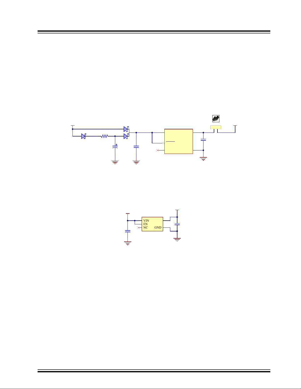
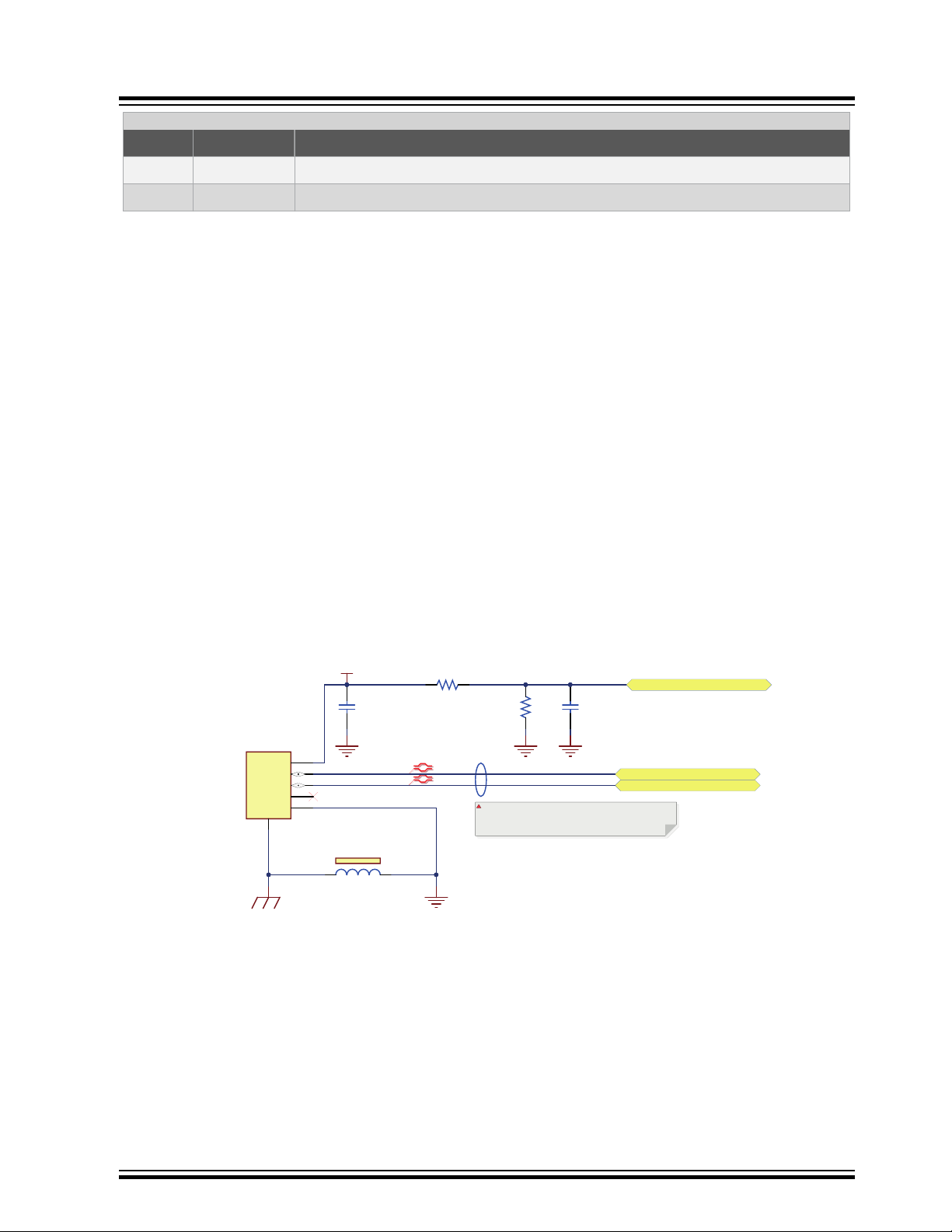
3.4.2 Power Supply Topology
3.4.2.1 Input Power
The ATSAMA5D27-WLSOM1-EK1 power source can come through a USB connector (J10) connected to a PC. This
USB power source is sufficient to supply the board in most applications.
Important: In case of an external device connected through the USB-B port, it is recommended to use
the 5V power supply input with an AC/DC wall adapter for the entire system rather than a PC or a USB
hub, which are limited to 500 mA typical.
ATSAMA5D27-WLSOM1-EK1
Baseboard Components
Jumper J16 is used to perform VDD_MAIN current measurements on the baseboard.
The following figure is a schematic of the power source.
Figure 3-4. VDD_MAIN Input Powering
3.4.2.2 Power Supply Requirements and Restrictions
Detailed information on the device power supplies is provided in tables “SAMA5D2 Power Supplies” and “Power
Supply Connections” in the SAMA5D2 Series datasheet.
3.4.2.3 Power-up and Power-down Considerations
Power-up and power-down considerations are described in section “Power Considerations” of the SAMA5D2 Series
datasheet.
Note: The power-up and power-down sequences provided in the SAMA5D2 Series datasheet must be respected for
reliable operation of the device. These are respected by the on-board MCP16502.
3.4.2.3.1 LPDDR2 Power-Off Sequence
The LPDDR2 power-off sequence must be controlled by software to preserve the LPDDR2 device.
In this sequence, the CKE signal should be low during the full period the power rails are powering down.
The power failure can be controlled by the embedded Voltage Supervisor (MIC842) and handled at system level (IRQ
on PD31). The LPDDR2 power-off sequence is applied using the bit LPDDR2_LPDDR3_PWOFF in the MPDDRC
Low-Power register (MPDDRC_LPR).
© 2019 Microchip Technology Inc.
User Guide
DS50002931A-page 10
Page 11
For more information, refer to the following documents:
JP4
RB160M-60TR
D6
1
2
3
BAT54C
D7
100R
04025%
R92
0.1uF
10V
0402
C15
VDD_MAIN
VIN
1
SHDN
3
GND
2
NC
4
VOUT
5
MCP1711/1.8V
U6
0.1uF
10V
0402
C18
VDDBU
0.22F
5.5V
C13
12
HDR-2.54 Male 1x2
J17
VDD_3V3
1uF
10V
0402
C17
1uF
10V
0402
C14
VDDFUSE
VIN
1
GND
2
EN
3
NC
4
VOUT
5
MIC5366-2.5YC5-TR
U4
• SAMA5D2 Series Data sheet available on https://www.microchip.com/, sections LPDDR2 Power Fail
Management and MPDDRC Low-Power Register
• Jedec Standard Low Power Double Data Rate 2 (LPDDR2), JESD209-2B
Note: An uncontrolled power-off sequence can be applied only up to 400 times in the life of an LPDDR2 device.
3.4.2.4 Backup Power Supply
The ATSAMA5D27-WLSOM1-EK1 features a power source in order to permanently power the backup area of the
SAMA5D2 device (refer to the SAMA5D2 Series datasheet). A super capacitor (C13) sustains such permanent power
to VDDBU when all system power sources are off.
Figure 3-5. VDDBU Powering Options
ATSAMA5D27-WLSOM1-EK1
Baseboard Components
3.4.2.5 VDDFUSE Regulator
The ATSAMA5D27-WLSOM-EK1 board embeds an LDO that delivers 2.5V to VDDFUSE for Fuse box programming
and for Secure Mode switching.
Figure 3-6. VDDFUSE Powering Options
3.4.3 Push Button Switches
The ATSAMA5D27-WLSOM1-EK1 features four push buttons:
• SW1– Wake-up push button connected to the SAMA5D27 WKUP pin, used to exit the processor from Backup
mode.
• SW2 – Reset push button. When pressed and released, the baseboard is reset.
• SW3 – Power-on/off button
• SW4 – User momentary push button connected to PIO PB2
© 2019 Microchip Technology Inc.
User Guide
DS50002931A-page 11
Page 12
Figure 3-7. System and User Push Buttons
1 4
2 3
TACT SPST
SW1
WKUP
1 4
2 3
TACT SPST
SW2
1 4
2 3
TACT SPST
SW3
nSTART_SOM
USER_BUTTON_PB 02
GND
1 4
2 3
TACT SPST
SW4
100R
04025%
R70
100R
04025%
R71
100R
04025%
R72
100R
04025%
R73
10k
0402
R74
NRST
100k
0402
R156
VDDBU
VDDBU
OE
1
A
2
Y
4
GND
3
VCC
5
NL17SZ125-D
U2
JP2
1
2
J8
10k
0402
1%
R77
VDD_3V3
0.1uF
10V 0402
C3
10k
0402
R82
DNP
QSPI_CS_PB6
NCS_QSPI
Jumper on = Disable
ATSAMA5D27-WLSOM1-EK1
Baseboard Components
3.4.4 Disable Boot
One jumper (J8) controls the selection (CS#) of the bootable memory components (QSPI) using a noninverting 3state buffer.
Figure 3-8. QSPI CS Disable Boot
3.4.5 Secure Digital Multimedia Card (SDMMC) Interface
3.4.5.1 Secure Digital Multimedia Card (SDMMC) Controller
The rule of operation is:
• SW2 (RESET) pressed and J8 open = booting from QSPI on WLSOM1
• SW2 (RESET) pressed and J8 closed = booting from external QSPI. The QSPI on WLSOM1 is disabled.
Refer to the SAMA5D2 Series data sheet for more information on standard boot strategies and sequencing.
The SD (Secure Digital) Card is a non-volatile memory card format used as a mass storage memory in mobile
devices.
The ATSAMA5D27-WLSOM1-EK1 features two Secure Digital Multimedia Card (SDMMC) interfaces that support the
MultiMedia Card (e.MMC) Specification V4.41, the SD Memory Card Specification V3.0, and the SDIO V3.0
specification. It is compliant with the SD Host Controller Standard V3.0 Specification.
© 2019 Microchip Technology Inc.
User Guide
DS50002931A-page 12
Page 13
• The SDMMC0 interface is connected to a standard SD card interface.
GND
i
SDMMC
Matched Net Lengths [Tolerance = 0.25mm]
68k
0402
5%
R81
4.7uF
10V
0402
C5
DAT3
1
CMD
2
VSS1
3
VDD
4
CLK
5
VSS2
6
DAT0
7
DAT1
8
DAT2
9
CD
10
WP
11
SHIELD
12
SD
J9
GND
VDD_3V3
10k
0402
1%
R84
10k
0402
1%
R83
10k
0402
1%
R76
68k
0402
5%
R80
68k
0402
5%
R79
68k
0402
5%
R78
VDDSDHC
SDMMC0_WP_PA12
SDMMC0_DAT2_PA04
SDMMC0_CMD_PA01
SDMMC0_DAT3_PA05
SDMMC0_CLK_PA00
SDMMC0_DAT0_PA02
SDMMC0_DAT1_PA03
SDMMC0_CD_PA13
10000pF
50V
0402
C23
22R 0402 1%
R75
22R 0402 1%
R94
22R 0402 1%
R96
22R 0402 1%
R157
22R 0402 1%
R158
22R 0402 1%
R159
0.1uF
10V
0402
C4
50Ω ± 10% single-ended trace impedance
10k
0402
1%
R93
0.1uF
10V
0402
C16
VDD_3V3
GNDGND
GND
VDD_3V3 VDDSDHCVDD_1V8
SDMMC0_VDDSEL_PA11 IN
1
VDD
2
GND
3
S1
4
D
5
S2
6
ADG849
U5
1uF
10V
0402
C28
IN=0: S1 Closed
IN=1: S2 Closed
• The SDMMC1 interface is connected to a WILC3000.
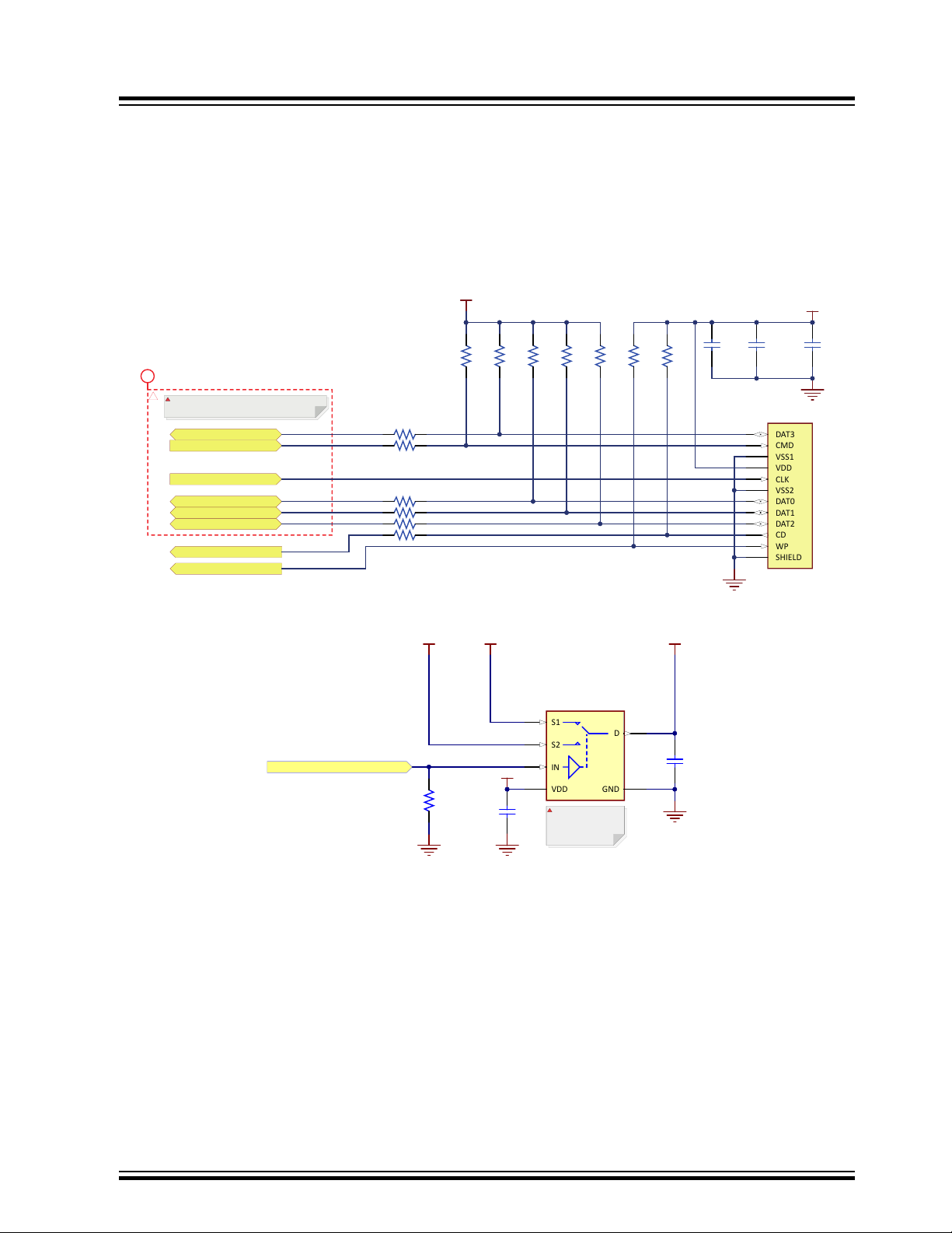
3.4.5.2 SDMMC0 Card Connector (J9)
The board provides a standard MMC/SD card connector, connected to SDMMC0. The SDMMC0 communication is
based on an 8-pin interface (clock, command, write protect, power switch and data (4)). A card detection switch is
included.
The figure below illustrates the SDMMC0 interface implementation.
Figure 3-9. SDMMC0 Schematic
ATSAMA5D27-WLSOM1-EK1
Baseboard Components
Figure 3-10. VDDSDHC Power Switch Schematic
© 2019 Microchip Technology Inc.
DS50002931A-page 13
User Guide
Page 14
Figure 3-11. Standard SD Socket J9 Location
ATSAMA5D27-WLSOM1-EK1
Baseboard Components
The table below describes the pin assignment of SD-CARD connector J9.
Table 3-3. SD-CARD Connector Pin Assignment
Pin No Mnemonic PIO Signal Description
1 DAT3 PA5 Data Line
2 CMD PA1 Command/Response Line
3 VSS1 – GROUND
4 VDDSDHC – Power Line (3.3V/1.8V)
5 CLK PA0 Clock Line
6 VSS2 – GROUND
7 DAT0 PA2 Data Line
8 DAT1 PA3 Data Line
9 DAT2 PA4 Data Line
10 CD PA13 Card Detect
© 2019 Microchip Technology Inc.
User Guide
DS50002931A-page 14
Page 15
...........continued
470R
04025%
R67
EARTH_ETH
GND_ETH
VDD_3V3
EARTH_ETH
EARTH_ETH
ETH_TX_P
ETH_TX_N
ETH_RX_P
ETH_RX_N
i
ETHERNET
ETH_LED0
GND
GND_ETH
0R
0402
R69
0.1uF
10V
0402
C2
0.1uF
10V
0402
C1
120R
BLM18PG121SN1D
FB5
DIFF100
DIFF100
DIFF100
DIFF100
TD+
TD-
RD-
RD+
TCT
RCT
1nF
75R75R
75R
75R
TX+
TX-
RX+
RX-
Green
Yellow
1
2
3
4
5
6
7
8
Right
Lift
3
1
2
5
6
4
10
9
8
SHD
11
12
JD2-0010NL
J6
C
ON RJ-45 JD2-0010NL
100Ω ±5Ω differential trace impedance
Routing top or bottom
Pin No Mnemonic PIO Signal Description
11 WP PA12 Write Protect
12 SHIELD – GROUND
3.4.6 Communication Interfaces
This section describes the signals and connectors related to the ETH and USB communication interfaces.
3.4.6.1 Ethernet 10/100 (GMAC) Port
The on-board ATSAMA5D27-WLSOM1 module integrates a 10/100 Mbps Ethernet Phy (KSZ8081RNA) allowing
direct connection to any 10/100 Mbps Ethernet-based Local Area Network, for full interaction with local servers and
wide area networks such as the Internet.
ETH signals from the WLSOM1 are connected to a RJ45 MagJack. Additionally, for monitoring and control purposes,
a LED functionality is carried on the RJ45 connector to indicate link status.
Figure 3-12. Ethernet 10/100 Interface Schematic
ATSAMA5D27-WLSOM1-EK1
Baseboard Components
© 2019 Microchip Technology Inc.
User Guide
DS50002931A-page 15
Page 16
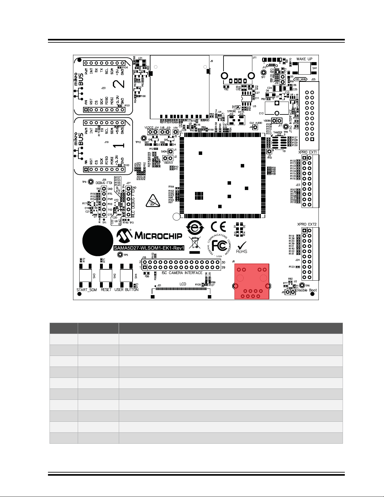
Figure 3-13. Ethernet 10/100 Connector J6 Location
ATSAMA5D27-WLSOM1-EK1
Baseboard Components
The table below describes the pin assignment of Ethernet connector J6.
Table 3-4. Ethernet RJ45 Connector Pin Assignment
Pin No Mnemonic Signal Description
1 TD+ Transmit positive differential pair
2 TCT Transmit differential pair decoupling capacitor
3 TD- Transmit negative differential pair
4 RD+ Receive positive differential pair
5 RCT Receive differential pair decoupling capacitor
6 RD- Receive negative differential pair
8 EARTH GROUND
9 YA Yellow LED anode. Connected to ETH_LED0
10 YK Yellow LED cathode. Connected to VDD_3V3 through 470R resistor.
11 GA Green LED anode (Not connected)
© 2019 Microchip Technology Inc.
User Guide
DS50002931A-page 16
Page 17
...........continued
USBA_N
USBA_P
GNDEARTH_USB_A
ID
4
VBUS
1
GND
5
D-
2
D+
3
0
0475890001
CON USB2.0 MICRO-AB FEMALE SMD R/A
J10
20pF
50V
0402
C6
VBUS_USBA
GND
200k
0402
1%
R86
100k
0402
R85
GND
0.1uF
10V
0402
C7
GND
USB_DETECT_PA16
USBA
120R
BLM18PG121SN1D
FB1
DIFF90
DIFF90
90Ω ±10% differential trace impedance
Routing top or bottom
Pin No Mnemonic Signal Description
12 GK Green LED cathode (Not connected)
SHD EARTH GROUND
3.4.6.2 USB Interfaces
The USB (Universal Serial Bus) is a hot-pluggable general-purpose high-speed I/O standard for computer
peripherals. The standard defines connector types, cabling, and communication protocols for interconnecting a wide
variety of electronic devices. The USB 2.0 Specification defines data transfer rates as high as 480 Mbps (also known
as High-Speed USB). A USB host bus connector uses four pins: a power supply pin (5V), a differential pair (D+ and
D- pins) and a ground pin.
The ATSAMA5D27-WLSOM1-EK1 features three USB communication ports named USB-A to USB-C:
• USB-A device interface
– One USB device standard Micro-AB connector
– Offers a VBUS detection function through the R81-R83 resistor ladder
– Used as a secondary power source and as a communication link for the ATSAMA5D27-WLSOM1-EK1, and
derives power from the PC over the USB cable. In most cases, this port is limited to 500 mA.
• USB-B (host port B high- and full-speed interface)
– One USB host type C connector
– Equipped with a 500 mA high-side power switch
• USB-C (High-Speed Inter-Chip/HSIC port)
– One USB high-speed host port with an HSIC interface
– Connected to 2 U.FL connectors
ATSAMA5D27-WLSOM1-EK1
Baseboard Components
3.4.6.3 USB-A Interface
The figure below shows the USB implementation on the USB-A port terminated on a Micro-AB type USB connector.
Figure 3-14. USB-A Device Interface Schematic
© 2019 Microchip Technology Inc.
User Guide
DS50002931A-page 17
Page 18
Figure 3-15. USB-A Device Connector J10 Location
ATSAMA5D27-WLSOM1-EK1
Baseboard Components
The table below describes the pin assignment of USB-A connector J10.
Table 3-5. USB-A Pin Assignment
Pin No Mnemonic PIO Signal Description
1 VBUS_USBA – Main 5V Input Supply
2 USBA_N HHSDMA USB Host Port A High Speed Data -
3 USBA_P HHSDPA USB Host Port A High Speed Data +
4 ID – Not connected
5 GND – GROUND
– USB_DETECT PA16 VBUS Insertion Detection
3.4.6.4 USB-B Interface and Power Switch
The figure below shows the USB implementation on the USB-B port terminated on USB Type A connector J11.
© 2019 Microchip Technology Inc.
User Guide
DS50002931A-page 18
Page 19
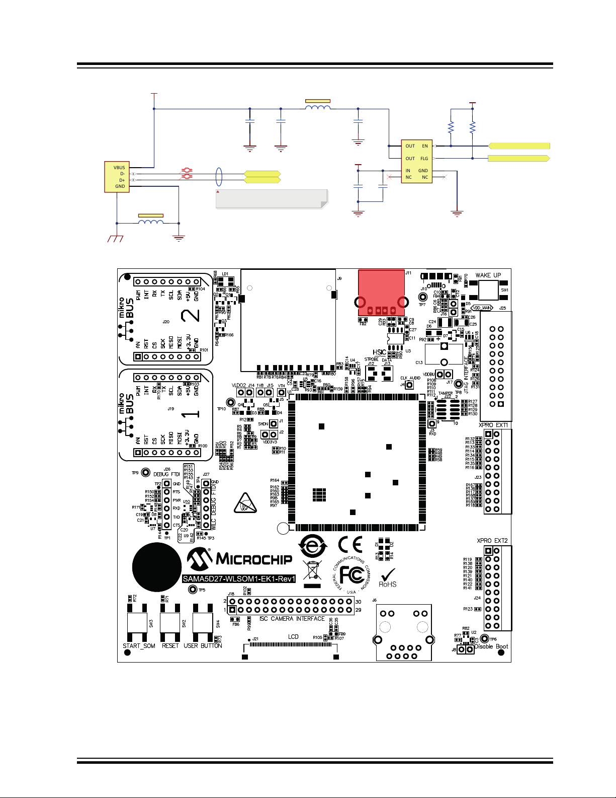
Figure 3-16. USB-B Host Interface Schematic
10k
0402
1%
R90
VBUS
1
GND
4
D-
2
D+
3
0
USB2.0 STD-A FEMALE
J11
GNDEARTH_USB_B
USBB_N
USBB_P
EN
1
FLG
2
GND
3
NC
4
NC
5
OUT
6
IN
7
OUT
8
USB Power Switch
MIC2025-1YM
U3
0.1uF
10V
0402
C8
GND
10uF
10V
0603
C9
GND
GND
0.1uF
10V
0402
C11
VDD_MAIN
USBB_POWER_EN_PA10
USBB_OVCUR_PA15
USB
B
10k
0402
1%
R89
VDD_3V3
120R
BLM18PG121SN1D
FB2
120R
BLM18PG121SN1D
FB3
10uF
10V
0603
C27
GND
10uF
10V
0603
C29
GND
VBUS_USBB
DIFF90
DIFF90
90Ω ±10% differential trace impedance
Routing top or bottom
Figure 3-17. USB-B Host Connector J11 Location
ATSAMA5D27-WLSOM1-EK1
Baseboard Components
The table below describes the pin assignment of USB-B connector J11.
© 2019 Microchip Technology Inc.
User Guide
DS50002931A-page 19
Page 20

Table 3-6. USB-B Pin Assignment
RF Coaxial U.FL Male
J12
U.FL
DNP
GND
RF Coaxial U.FL Male
J13
U.FL
DNP
GND
DATA
STROBE
i
HSIC
Matched Net Lengths [Tolerance = 0.25mm]
50Ω ± 10% single-ended trace impedance
Pin No Mnemonic PIO Signal Description
1 VBUS_USBB – Main 5V Input Supply
2 USBB_N HHSDMB USB Host Port B High Speed Data -
3 USBB_P HHSDPB USB Host Port B High Speed Data +
4 GND – GROUND
– USBB_POWER_EN PA14 USBB Power Switch Enable
– USBB_OVCUR PA15 VBUS Over Current Interrupt
3.4.6.5 HSIC Interface
High-Speed Inter-Chip (HSIC) is a standard for USB chip-to-chip interconnect with a 2-signal (strobe, data) source
synchronous serial interface using 240 MHz DDR signaling to provide only high-speed 480 Mbps data rate.
The interface operates at high speed, 480 Mbps, and is fully compatible with existing USB software stacks. It meets
all data transfer needs through a single unified USB software stack.
The HSIC port is connected to 2 U.FL connectors (not populated by default).
Figure 3-18. HSIC Interface Schematic
ATSAMA5D27-WLSOM1-EK1
Baseboard Components
© 2019 Microchip Technology Inc.
User Guide
DS50002931A-page 20
Page 21

Figure 3-19. HSIC Connectors J12 and J13 Location
ATSAMA5D27-WLSOM1-EK1
Baseboard Components
3.5 External Interfaces
3.5.1 LCD TFT Interface
The ATSAMA5D27-WLSOM1-EK1 provides an FPC connector with 18 bits of data and control signals to the LCD
interface.
This connector is used to connect to an LCD display type AC320005-5.
A 50-pin FPC (J21) header is provided on the baseboard to interface the LCD module with the 18-bit parallel RGB
mode and is used to connect to an LCD display type AC320005-5.
The connector provides two PIOs as interrupts, one SPI and a TWI port to interface the MaXTouch® touch controller
or QTouch® button controller embedded on the LCD module.
In order to operate correctly from the processor with various LCD modules, two voltage lines are available: 3.3V and
5VCC (default). Both are selected by 0R resistors R107 and FB9.
© 2019 Microchip Technology Inc.
User Guide
DS50002931A-page 21
Page 22

Figure 3-20. LCD Interface Schematic
I2C Signals Distribution
TWCK1_LCD_PD20
TWD1_LCD_PD19
22R 0402 1%
R54
22R 0402 1%
R55
2.2k
0402
5%
R49
2.2k
0402
5%
R48
VDD_3V3
PD19
PD20
ISC/LCD Signals Distribution
22R 0402 1%
R15
22R 0402 1%
R16
22R 0402 1%
R18
22R 0402 1%
R19
22R 0402 1%
R20
22R 0402 1%
R21
22R 0402 1%
R17
LCD_D2_PC10
LCD_D3_PC11
LCD_D4_PC12
LCD_D5_PC13
LCD_D6_PC14
LCD_D7_PC15
LCD_D10_PC16
LCD_D11_PC17
LCD_D12_PC18
LCD_D13_PC19
LCD_D14_PC20
LCD_D15_PC21
LCD_D18_PC22
LCD_D19_PC23
LCD_D20_PC24
LCD_ID_PC09
22R 0402 1%
R22
22R 0402 1%
R23
22R 0402 1%
R24
22R 0402 1%
R27
22R 0402 1%
R28
22R 0402 1%
R29
22R 0402 1%
R26
22R 0402 1%
R25
PC21
PC22
100R 0402 5%
R31
22R 0402 1%
R30PC25
LCD_D21_PC25
PC09
PC10
PC11
PC12
PC13
PC14
PC15
PC16
PC17
PC18
PC19
PC20
PC23
PC24
SPI1 Signals Distribution
PC01
PC02
PC03
SPI1_SPCK_LCD_PC01
SPI1_MISO_LCD_PC03
SPI1_MOSI_LCD_PC02
SPI1_NPCS2_LCD_PC06
22R 0402 1%
R6
22R 0402 1%
R9
22R 0402 1%
R12PC06
39R 0402 1%
R3
LCD INTERFACE
TWCK1_LCD_PD20
TWD1_LCD_PD19
1
2
3
4
5
6
7
8
9
10
11
12
13
14
15
16
17
18
19
20
21
22
23
24
25
26
27
28
29
30
31
32
33
34
35
36
37
38
39
40
41
42
43
44
45
46
47
48
49
50
MNT
FFC
FFC/FPC 50P Female
J21
GND
0R 0402
R105
LCD_nRST
NRST
LCD_D2_PC10
LCD_D3_PC11
LCD_D4_PC12
LCD_D5_PC13
LCD_D6_PC14
LCD_D7_PC15
LCD_D10_PC16
LCD_D11_PC17
LCD_D12_PC18
LCD_D13_PC19
LCD_D14_PC20
LCD_D15_PC21
LCD_D22_PC26
LCD_D23_PC27
LCD_EN_PC29
LCD_IRQ1_PB04
LCD_PWM_PC28
LCD_VSYNC_PC30
LCD_HSYNC_PC31
LCD_DATA_EN_PD01
CD_PCLK_PD00
LCD_D18_PC22
LCD_D19_PC23
LCD_D20_PC24
LCD_D21_PC25
LCD_ID_PC09
SPI1_SPCK_LCD_PC01
SPI1_MISO_LCD_PC03
SPI1_MOSI_LCD_PC02
SPI1_NPCS2_LCD_PC06
VDD_MAIN
VDD_3V3
0R 0402
DNP
R107
DNP
LCD_IRQ2_PA17
i
LCD
Matched Net Lengths [Tolerance = 1.27mm]
1k
BLM18AG102SN1D
FB8
0.1uF
10V
0402
C32
DNP
27pF
50V
0402
C33
DNP
1uF
10V
0402
C34
DNP
100R
0402
1%
R106
DNP
GND GNDGND
30R
FB9
0.1uF
10V
0402
C35
GND
1uF
10V
0402
C36
GND
ATSAMA5D27-WLSOM1-EK1
Baseboard Components
© 2019 Microchip Technology Inc.
DS50002931A-page 22
User Guide
Page 23

Figure 3-21. LCD Connector J21 Location
ATSAMA5D27-WLSOM1-EK1
Baseboard Components
The table below describes the pin assignment of LCD connector J21.
Table 3-7. LCD Connector Pin Assignment
Pin No Signal PIO Signal RGB Interface Function
1 ID PC9 ID –
2 – – GND Ground
3 NC – NC Not connected
4 NC – NC Not connected
5 LCDDAT2 PC10 D2 Data Line (BLUE 2)
6 LCDDAT3 PC11 D3 Data Line (BLUE 3)
7 – – GND Ground
8 LCDDAT4 PC12 D4 Data Line (BLUE 4)
9 LCDDAT5 PC13 D5 Data Line (BLUE 5)
10 LCDDAT6 PC14 D6 Data Line (BLUE 6)
© 2019 Microchip Technology Inc.
User Guide
DS50002931A-page 23
Page 24

ATSAMA5D27-WLSOM1-EK1
Baseboard Components
...........continued
Pin No Signal PIO Signal RGB Interface Function
11 LCDDAT7 PC15 D7 Data Line (BLUE 7)
12 – – GND Ground
13 NC – NC Not connected
14 NC – NC Not connected
15 LCDDAT10 PC16 D10 Data Line (GREEN 2)
16 LCDDAT11 PC17 D11 Data Line (GREEN 2)
17 – – GND Ground
18 LCDDAT12 PC18 D12 Data Line (GREEN 4)
19 LCDDAT13 PC19 D13 Data Line (GREEN 5)
20 LCDDAT14 PC20 D14 Data Line (GREEN 6)
21 LCDDAT15 PC21 D15 Data Line (GREEN 7)
22 – – GND Ground
23 NC – NC Not connected
24 NC – NC Not connected
25 LCDDAT18 PC22 D18 Data Line (RED 2)
26 LCDDAT19 PC23 D19 Data Line (RED 3)
27 – – GND Ground
28 LCDDAT20 PC24 D20 Data Line (RED 4)
29 LCDDAT21 PC25 D21 Data Line (RED 5)
30 LCDDAT22 PC26 D22 Data Line (RED 6)
31 LCDDAT23 PC27 D23 Data Line (RED 7)
32 – – GND Ground
33 LCDPCK PD0 PCLK Pixel Clock
34 LCDVSYNC PC30 VSYNC/CS Vertical Synchro
35 LCDHSYNC PC31 HSYNC/WE Horizontal Synchro
36 LCDDEN PD1 DATA_ENABLE Data Enable
37 SPI_SPCK PC1 SPI CLOCK SPI Clock
38 SPI_MOSI PC2 SPI MOSI SPI Master OUT Slave IN
39 SPI_MISO PC3 SPI MISO SPI Master IN Slave OUT
40 SPI_NPCS0 PC6 SPI CS SPI Chip Select
41 LCDDISP PC29 ENABLE Display Enable Signal
42 TWD PD19 TWI_DATA I²C Data Line (maXTouch)
43 TWCK PD20 TWI_CLOCK I²C clock Line (maXTouch)
44 GPIO PB4 IRQ1 maXTouch Interrupt Line
45 GPIO PA17 IRQ2 Interrupt Line for other I²C devices
© 2019 Microchip Technology Inc.
User Guide
DS50002931A-page 24
Page 25

...........continued
ISC CAMERA INTERFACE
TWCK1_ISC_PD20
ISC_D5_PC14
ISC_D7_PC16
ISC_D9_PC18
ISC_D11_PC20
VDD_3V3
1
2
3
4
5
6
7
8
9
10
11
12
13
14
15
16
17
18
19
20
22
2123
24
25
26
27
28
29
30
J18
DNP
TWD1_ISC_PD19
ISC_MCK_PC24
ISC_VSYNC_PC22
ISC_HSYNC_PC23
ISC_PCK_PC21
ISC_D4_PC13
ISC_D6_PC15
ISC_D8_PC17
ISC_D10_PC19
ISC_PWD_XPRO_LED_15_PC07
39R 0402 1%
R102
39R 0402 1%
R99
120R
BLM18PG121SN1D
FB6
ISC_NRST_PA09
ISC_D1_PC10
ISC_D3_PC12
ISC_D0_PC09
ISC_D2_PC11
I2C Signals Distribution
TWD1_ISC_PD19
TWCK1_ISC_PD20
22R 0402 1%
R56
22R 0402 1%
R57
2.2k
0402
5%
R49
2.2k
0402
5%
R48
VDD_3V3
PD19
PD20
ISC/LCD Signals Distribution
22R 0402 1%
R35
22R 0402 1%
R36
22R 0402 1%
R37
22R 0402 1%
R38
ISC_D5_PC14
ISC_D7_PC16
ISC_D9_PC18
ISC_D11_PC20
ISC_PCK_PC21
ISC_VSYNC_PC22
ISC_HSYNC_PC23
ISC_MCK_PC24
ISC_D4_PC13
ISC_D6_PC15
ISC_D8_PC17
ISC_D10_PC19
22R 0402 1%
R39
22R 0402 1%
R40
22R 0402 1%
R41
22R 0402 1%
R44
22R 0402 1%
R45
22R 0402 1%
R46
22R 0402 1%
R43
22R 0402 1%
R42
PC13
PC14
PC15
PC16
PC17
PC18
PC19
PC20
PC23
PC24
PC21
PC22
i
ISC
Matched Net Lengths [Tolerance = 1.27mm]
22R 0402 1%
R47
22R 0402 1%
R32
22R 0402 1%
R33
22R 0402 1%
R34
ISC_D1_PC10
ISC_D3_PC12
ISC_D0_PC09
ISC_D2_PC11
PC09
PC10
PC11
PC12
Pin No Signal PIO Signal RGB Interface Function
46 LCDPWM PC28 PWM Backlight Control
47 RESET NRST RESET Reset for both display and maXTouch
48 Main_5V/3.3V – VCC 3.3V or 5V supply (5V by default)
49 Main_5V/3.3V – VCC 3.3V or 5V supply (5V by default)
50 – – GND Ground
3.5.2 Image Sensor (ISC) Interface
This section describes the signals and connectors related to the ISC interface.
The Image Sensor Controller (ISC) system manages incoming data from a parallel or serial CSI-2 based CMOS/CCD
sensor. The system supports a single active interface, as well as the ITU-R BT 656/1120 422 protocol with an 8-bit or
10-bit data width and raw Bayer format. The internal image processor includes adjustable white balance, color filter
array interpolation, color correction, gamma correction, 12-bit to 10-bit compression, programmable color space
conversion, as well as horizontal and vertical chrominance subsampling module.
Figure 3-22. Image Sensor Camera Interface Schematic
ATSAMA5D27-WLSOM1-EK1
Baseboard Components
© 2019 Microchip Technology Inc.
User Guide
DS50002931A-page 25
Page 26

Figure 3-23. ISC Connector J18 Location
ATSAMA5D27-WLSOM1-EK1
Baseboard Components
The table below describes the pin assignment of ISC connector J18.
Table 3-8. ISC Connector Pin Assignment
Function PIO Signal Pin No Signal PIO Function
3.3V – VDD_3V3 1 2 GND – GROUND
3.3V – VDD_3V3 3 4 GND – GROUND
Reset PA9 ISC_nRST 5 6 ISC_PWD PC7 Power Down
TWI Clock PD20 TWCK 7 8 TWD PD19 TWI Data
GROUND – GND 9 10 ISC_MCK PC24 Master Clock
GROUND – GND 11 12 ISC_VSYNC PC22 Vertical Synchro
GROUND – GND 13 14 ISC_HSYNC PC23 Horizontal Synchro
GROUND – GND 15 16 ISC_PCK PC21 Clock
GROUND – GND 17 18 ISC_D0 PC9 Data0
Data1 PC10 ISC_D1 19 20 ISC_D2 PC11 Data2
© 2019 Microchip Technology Inc.
User Guide
DS50002931A-page 26
Page 27

...........continued
GREEN
BLUE
2
1
RED
4
3
RED, GREEN, BLUE
LD1
LED_RGB_CL
V1A
VDD_3V3
3
1
2
BSS138
Q1
GND
100R
04025%
R62
3
1
2
BSS138
Q2
GND
100R
04025%
R63
3
1
2
BSS138
Q3
GND
100R
04025%
R64
2.2k
04025%
R65
2.2k
04025%
R66
1k
04025%
R68
RED_LED_PA06
GREEN_LED_PA07
BLUE_LED_PA08
10k
0402
1%
R95
10k
0402
1%
R166
GND
GND
Function PIO Signal Pin No Signal PIO Function
Data3 PC12 ISC_D3 21 22 ISC_D4 PC13 Data4
Data5 PC14 ISC_D5 23 24 ISC_D6 PC15 Data6
Data7 PC16 ISC_D7 25 26 ISC_D8 PC17 Data8
Data9 PC18 ISC_D9 27 28 ISC_D10 PC19 Data10
Data11 PC20 ISC_D11 29 30 GND – GROUND
3.5.3 RGB LED
The ATSAMA5D27-WLSOM1-EK1 features one RGB LED which can be controlled by the user. The three LED
cathodes are controlled via GPIOs or Timer/Counter pins (only for red and green LEDs).
Figure 3-24. RGB LED Schematic
ATSAMA5D27-WLSOM1-EK1
Baseboard Components
© 2019 Microchip Technology Inc.
User Guide
DS50002931A-page 27
Page 28

Figure 3-25. RGB LED Device Location
ATSAMA5D27-WLSOM1-EK1
Baseboard Components
The table below describes the pin assignment of RGB LED.
Table 3-9. RGB LED Pin Assignment
Signal PIO Function
RED_LED PA6 GPIO/TIOA5
GREEN_LED PA7 GPIO/TIOB5
BLUE_LED PA8 GPIO
3.6 Debugging Capabilities
The ATSAMA5D27-WLSOM1-EK1 includes two main debugging interfaces to provide debug-level access to the
SAMA5D2:
• One JTAG interface connected from the MPU using connector J25.
• One UART interface connected from the MPU using connector J26.
3.6.1 Debug JTAG
This section describes the signals and connectors related to the JTAG interface.
© 2019 Microchip Technology Inc.
User Guide
DS50002931A-page 28
Page 29

100k
0402
R124
100R
R125
100k
0402
R126
100k
0402
R131
JTAG_TMS_PD30
JTAG_TCK_PD27
JTAG_TDO_PD29
JTAG_TDI_PD28
NRST
VDD_3V3
1
2
3
4
5
6
7
8
9
10
11
12
13
14
15
16
17
18
19
20
HDR-2.54 Male 2x10
J25
ATSAMA5D27-WLSOM1-EK1
Baseboard Components
A 20-pin JTAG header is provided on the baseboard to facilitate software development and debugging using various
JTAG emulators. The interface signals have a voltage level of 3.3V.
Figure 3-26. JTAG Interface Schematic
Figure 3-27. JTAG Connector J25 Location
User Guide
The table below describes the pin assignment of JTAG connector J25.
© 2019 Microchip Technology Inc.
DS50002931A-page 29
Page 30

ATSAMA5D27-WLSOM1-EK1
Baseboard Components
Table 3-10. JTAG Connector Pin Assignment
Pin No Function PIO Signal
1 3.3V Supply Voltage – VDD_3V3
2 3.3V Supply Voltage – VDD_3V3
3 Not used – NC
4 GROUND – GND
5 JTAG data input into target processor PD28 JTAG TDI
6 GROUND – GND
7 JTAG mode set input into target processor PD30 JTAG TMS
8 GROUND – GND
9 JTAG clock signal into target processor PD27 JTAG TCK
10 GROUND – GND
11 Not used – NC
12 GROUND – GND
13 JTAG data output from target processor PD29 JTAG TDO
14 GROUND – GND
15 Active-low reset signal. Target processor reset signal. NRST NRST
16 GROUND – GND
17 Not used – NC
18 GROUND – GND
19 Not used – NC
20 GROUND – GND
3.6.2 Debug UART
The ATSAMA5D27-WLSOM1-EK1 board has a dedicated serial port for debugging, which is accessible through the
6-pin male header J26. Various interfaces can be used as a USB/Serial DBGU port bridge, such as FTDI TTL-232R
USB to TTL serial cable or basic breakout board for the RS232/USB converter.
© 2019 Microchip Technology Inc.
User Guide
DS50002931A-page 30
Page 31

Figure 3-28. SAMA5D2 Debug FTDI Interface Schematic
1
2
3
4
5
6
HDR-2.54 Male 1x6
J26
68k
0402
R148
68k
0402
DNP
R150
DNP
68k
0402
R146
68k
0402
DNP
R144
DNP
0R
0402
DNP
R152
DNP
0R
0402
DNP
R154
DNP
VDD_3V3 VDD_MAIN
OE
1
A
2
Y
4
GND
3
VCC
5
NL17SZ126-D
U7
0.1uF
10V 0402
C21
VDD_3V3
DBGU_TXD
DBGU_RXD
DBGU_TX_PB27
OE
1
A
2
Y
4
GND
3
VCC
5
NL17SZ126-D
U8
0.1uF
10V
0402
C19
VDD_3V3
DBGU_RX_PB26
DBGU_RXD
DBGU_TXD
DBGU_CTS
DBGU_RTS
TP2
TP1
100k
0402
R171
ATSAMA5D27-WLSOM1-EK1
Baseboard Components
Two Tri-State Buffers are available on TX and RX lines in order to protect the system against any leakage when an
FTDI connector is present and when the system is not started yet.
R152 and R154 are optional (not implemented) resistors that can be used for power selection. Power can be
delivered either by the ATSAMA5D27-WLSOM1-EK1 board or by the debug interface tool. To avoid malfunction
between the debug interface (e.g., FTDI) and the on-board power system, ensure that the voltage level selected
corresponds to the application requirements.
© 2019 Microchip Technology Inc.
User Guide
DS50002931A-page 31
Page 32

Figure 3-29. FTDI Debug Connector J26 Location
ATSAMA5D27-WLSOM1-EK1
Baseboard Components
The table below describes the pin assignment of FTDI connector J26.
Table 3-11. FTDI Connector Pin Assignment
Pin No Mnemonic PIO Signal Description
1 DBGU_CTS RFU Handshake Input
2 DBGU_TXD PB27 RS232 serial data output signal
3 DBGU_RXD PB26 RS232 serial data input signal
4 VDD – 3.3V or 5V Supply
5 DBGU_RTS RFU Handshake Output
6 GND – GROUND
3.6.3 WILC3000 Debug UART
The ATSAMA5D27-WLSOM1-EK1 has a dedicated serial port for WILC3000 Module debugging, which is accessible
through the 6-pin male header J27 (not populated by default).
© 2019 Microchip Technology Inc.
User Guide
DS50002931A-page 32
Page 33

Figure 3-30. WILC3000 Debug FTDI Interface Schematic
1
2
3
4
5
6
HDR-2.54 Male 1x6
J26
68k
0402
R148
68k
0402
DNP
R150
DNP
68k
0402
R146
68k
0402
DNP
R144
DNP
0R
0402
DNP
R152
DNP
0R
0402
DNP
R154
DNP
VDD_3V3 VDD_MAIN
OE
1
A
2
Y
4
GND
3
VCC
5
NL17SZ126-D
U7
0.1uF
10V 0402
C21
VDD_3V3
DBGU_TXD
DBGU_RXD
DBGU_TX_PB27
OE
1
A
2
Y
4
GND
3
VCC
5
NL17SZ126-D
U8
0.1uF
10V
0402
C19
VDD_3V3
DBGU_RX_PB26
DBGU_RXD
DBGU_TXD
DBGU_CTS
DBGU_RTS
TP2
TP1
100k
0402
R171
ATSAMA5D27-WLSOM1-EK1
Baseboard Components
© 2019 Microchip Technology Inc.
User Guide
DS50002931A-page 33
Page 34

Figure 3-31. FTDI WILC Connector J27 Location
ATSAMA5D27-WLSOM1-EK1
Baseboard Components
The table below describes the pin assignment of WILC3000 FTDI connector J27.
Table 3-12. WILC3000 FTDI Connector Pin Assignment
Pin No Mnemonic PIO Signal Description
1 WILCFTDI_CTS RFU Handshake Input
2 WILCFTDI_TXD TXD_WILC_DBGU RS232 serial data output signal
3 WILCFTDI_RXD RXD_WILC_DBGU RS232 serial data input signal
4 VDD – 3.3V or 5V Supply
5 WILCFTDI_RTS RFU Handshake Output
6 GND – GROUND
3.7 PIO Usage on Expansion Connectors
This section describes the signals and connectors related to the PIO usage on expansion connectors.
© 2019 Microchip Technology Inc.
User Guide
DS50002931A-page 34
Page 35

The baseboard includes numerous peripherals. Many of these are connected to the GPIO block so that the I/O pins
1
2
3
4
5
6
7
8
9
10
FTS-105-01-L-DV
J22
330R
R108
330R
R109
330R
R110
330R
R111
330R
R127
330R
R128
0R
R112
0R
R129
0R
R130
COMP_N
COMP_P
PIOBU2
PIOBU4
PIOBU6
PIOBU7
PIOBU3
PIOBU5
PIOBU1
can be configured to carry out many alternative functions. This provides great flexibility to select a function
multiplexing scheme for the pins that satisfy the interface need for a particular application.
Note that most pins are configured as GPIO inputs, with a 100 KOhm pull-up resistor, after reset.
3.7.1 Tamper Interface
The ATSAMA5D27-WLSOM1-EK1 features seven tamper pins for static or dynamic intrusion detection and two
analog pins for comparison.
For a description of intrusion detection, refer to the SAMA5D2 data sheet, chapter “Security Module (SECUMOD)”.
Figure 3-32. Tamper Interface Schematic
Figure 3-33. Tamper Connector J22 Location
ATSAMA5D27-WLSOM1-EK1
Baseboard Components
The table below describes the pin assignment of Tamper connector J22.
© 2019 Microchip Technology Inc.
User Guide
DS50002931A-page 35
Page 36

Table 3-13. Tamper Connector Pin Assignment
TWCK1_mBUS1_PD20
TWD1_mBUS1_PD19
MikroBus1 AN
TWCK
TWD
URXD
UTXD
MikroBus1 PWM
MikroBus1 RST
MikroBus1 CS
MikroBus1 SCK
MikroBus1 MISO
MikroBus1 MOSI
MikroBus1 INT
MIKROBUS1
AN
1
RST
2
CS
3
SCK
4
MISO
5
MOSI
6
+3.3V
7
GND
8
PWM
16
INT
15
RX
14
TX
13
SCL
12
SDA
11
+5V
10
GND
9
mikroBUS HOST
J19
INT_mBUS1_PD02
RST_mBUS1_PB31
AN_mBUS1_PD25
URXD3_mBUS1_PB11
SPI1_SPCK_mBUS1_PC01
SPI1_MOSI_mBUS1_PC02
SPI1_MISO_mBUS1_PC03
SPI1_NPCS1_mBUS1_PC05
PWM_mBUS1_PA30
VDD_MAIN
VDD_3V3
0R
0402
R103
0R
0402
R100
UTXD3_mBUS1_PB12
100k
0402
R170
VDD_3V3
Signal Pin No Signal
COMP_N 1 2 PIOBU1
COMP_P 3 4 PIOBU4
PIOBU5 5 6 PIOBU6
PIOBU3 7 8 PIOBU2
PIOBU7 9 10 GND
3.7.2 mikroBUS Interfaces
The ATSAMA5D27-WLSOM1-EK1 hosts two pairs of 8-pin female headers acting as mikroBUS interfaces. The
mikroBUS standard defines the main board sockets and add-on boards, or Click boards, used for interfacing
microprocessors with integrated modules having proprietary pin configuration and silkscreen markings. The pinout
consists of three groups of communication pins (SPI, UART and TWI), four additional pins (PWM, interrupt, analog
input and reset) and two power groups (+3.3V and GND on the left, and 5V and GND on the right 1x8 header).
Figure 3-34. mikroBUS1 Interface Schematic
ATSAMA5D27-WLSOM1-EK1
Baseboard Components
© 2019 Microchip Technology Inc.
User Guide
DS50002931A-page 36
Page 37

Figure 3-35. mikroBUS1 Connector J19 Location
ATSAMA5D27-WLSOM1-EK1
Baseboard Components
The table below describes the pin assignment of mikroBUS1 connector J19.
Table 3-14. mikroBUS1 Connector Pin Assignment
Function PIO Signal Pin No Signal PIO Function
Analog Input PD25 mikroBUS1_AN 1 16 mikroBUS1_PWM PA30 PWM
Reset PB31 mikroBUS1_RST 2 15 mikroBUS1_INT PD2 Interrupt
SPI Chip Select PC5 mikroBUS1_CS 3 14 URXD PB12 UART Receive
SPI Clock PC1 mikroBUS1_SCK 4 13 UTXD PB11 UART Transmit
SPI MISO PC3 mikroBUS1_MISO 5 12 TWCK PD20 TWI Clock
SPI MOSI PC2 mikroBUS1_MOSI 6 11 TWD PD19 TWI Data
3.3V – VDD_3V3 7 10 VDD_MAIN – 5V
GROUND – GND 8 9 GND – GROUND
© 2019 Microchip Technology Inc.
User Guide
DS50002931A-page 37
Page 38

Figure 3-36. mikroBUS2 Interface Schematic
TWCK1_mBUS2_PD20
TWD1_mBUS2_PD19
URXD
UTXD
MikroBus2 AN
MikroBus2 RST
MikroBus2 CS
MikroBus2 SCK
MikroBus2 MISO
MikroBus2 MOSI
MikroBus2 PWM
MikroBus2 INT
MIKROBUS2
TWCK
TWD
AN
1
RST
2
CS
3
SCK
4
MISO
5
MOSI
6
+3.3V
7
GND
8
PWM
16
INT
15
RX
14
TX
13
SCL
12
SDA
11
+5V
10
GND
9
mikroBUS HOST
J20
AN_mBUS2_PD26
URXD0_mBUS2_PB29
SPI1_NPCS0_mBUS2_PC04
SPI1_SPCK_mBUS2_PC01
SPI1_MOSI_mBUS2_PC02
SPI1_MISO_mBUS2_PC03
INT_mBUS2_PB03
PWM_mBUS2_PA31
VDD_MAINVDD_3V3
0R
0402
R104
0R
0402
R101
UTXD0_mBUS2_PB28
RST_mBUS2_PC00
Figure 3-37. mikroBUS2 Connector J20 Location
ATSAMA5D27-WLSOM1-EK1
Baseboard Components
The table below describes the pin assignment of mikroBUS2 connector J20.
Table 3-15. mikroBUS2 Connectors Pin Assignment
Function PIO Signal Pin No Signal PIO Function
Analog Input PD26 mikroBUS2_AN 1 16 mikroBUS2_PWM PA31 PWM
© 2019 Microchip Technology Inc.
User Guide
DS50002931A-page 38
Page 39

...........continued
XPRO EXT1
0R
R113
XPRO EXT2
0R
R114
0R
R116
0R
R117
DNP
100R
R115
100R
R118
0R
R136
0R
R137
0R
R132
0R
R133
0R
R135
100R
R134
VDD_3V3
0R
R119
0R
R120
0R
R122
100R
R123
0R
R138
0R
R139
0R
R141
VDD_3V3
PTC_COL2_PD13
PTC_COL0_PD11
XPRO_LED_7_PB30
PTC_COL4_PD15
PTC_COL6_PD17
XPRO_LED_17_PB01
PTC_COL6_PD17
PTC_COL7_PD18
PTC_COL5_PD16
XPRO_LED_8_PB00
PTC_COL3_PD14
PTC_COL1_PD12
0R
R121
0R
R140
PTC_ROW0_PD03
PTC_ROW2_PD05
PTC_ROW4_PD07
PTC_ROW6_PD09
PTC_ROW1_PD04
PTC_ROW3_PD06
PTC_ROW5_PD08
PTC_ROW7_PD10
ISC_PWD_XPR
O_LED_15_PC07
TWCK1_XPRO_PD20TWD1_XPRO_PD19
1
2
3
4
5
6
7
8
9
10
11
12
13
14
15
16
17
18
19
20
HDR-2.54 Male 2x10 RA Rotated 180
J24
1
2
3
4
5
6
7
8
9
10
11
12
13
14
15
16
17
18
19
20
HDR-2.54 Male 2x10 RA Rotated 180
J23
XPRO_LED_2_PA14
0R
R167
0R
R168
DNP
0R
R169
DNP
Function PIO Signal Pin No Signal PIO Function
Reset PC0 mikroBUS2_RST 2 15 mikroBUS2_INT PB3 Interrupt
SPI Chip Select PC4 mikroBUS2_CS 3 14 URXD PB28 UART Receive
SPI Clock PC1 mikroBUS2_SCK 4 13 UTXD PB29 UART Transmit
SPI MISO PC3 mikroBUS2_MISO 5 12 TWCK PD20 TWI Clock
SPI MOSI PC2 mikroBUS2_MOSI 6 11 TWD PD19 TWI Data
3.3V – VDD_3V3 7 10 VDD_MAIN – 5V
GROUND – GND 8 9 GND – GROUND
3.7.3 Expansion Header Interfaces
The ATSAMA5D27-WLSOM1-EK1 can host two connectors to interface with standard Xplained Pro extensions and,
in particular, with QT Xplained Pro Extension boards.
The following QT Xplained Pro Extensions boards are compatible with the interfaces:
• QT1 Xplained Pro Extension Kit (ATQT1-XPRO)
• QT2 Xplained Pro Extension Kit (ATQT2-XPRO)
• QT6 Xplained Pro Extension Kit (ATQ6-XPRO)
Figure 3-38. Expansion Header Interface Schematic
ATSAMA5D27-WLSOM1-EK1
Baseboard Components
© 2019 Microchip Technology Inc.
User Guide
DS50002931A-page 39
Page 40

Figure 3-39. XPRO Connectors J23 and J24 Location
ATSAMA5D27-WLSOM1-EK1
Baseboard Components
The table below describes the pin assignment of XPRO_EXT1 connector J23.
Table 3-16. EXT_XPRO_1 Connector Pin Assignment
Function PIO Signal Pin No Signal PIO Function
NC – NC 1 2 GND – GROUND
PTC COL PD11 PTC_COL0_PD11 3 4 PTC_COL1_PD12 PD12 PTC COL
PTC COL PD13 PTC_COL2_PD13 5 6 PTC_COL3_PD14 PD14 PTC COL
PTC LED PB30 XPRO_LED_7_PB30 7 8 XPRO_LED_17_PB01 PB1 PTC LED
PTC COL PD15 PTC_COL4_PD115 9 10 PTC_COL5_PD16 PD16 PTC COL
TWI Data PD19 TWD1_XPRO_PD19 11 12 TWCK1_XPRO_PD20 PD20 TWI Clock
NC – NC 13 14 NC – NC
PTC LED PA14 XPRO_LED_2_PA14
PTC COL
© 2019 Microchip Technology Inc.
(1)
PD17 PTC_COL0_PD11 PTC_COL7_PD18 PD18 PTC COL
15 16
User Guide
PTC_COL6_PD17 PD17 PTC COL
DS50002931A-page 40
(1)
Page 41

ATSAMA5D27-WLSOM1-EK1
Baseboard Components
...........continued
Function PIO Signal Pin No Signal PIO Function
PTC LED PB0 XPRO_LED_8_PB00 17 18
PTC_COL7_PD18 PD18 PTC COL
PTC_COL6_PD17 PD17 PTC COL
GROUND – GND 19 20 VDD_3V3 – 3.3V
Note:
1. Not the default setting.
The table below describes the pin assignment of XPRO_EXT2 connector J24.
Table 3-17. EXT_XPRO_2 Connector Pin Assignment
Function PIO Signal Name Pin No Signal Name PIO Function
NC – NC 1 2 GND – GROUND
PTC ROW PD3 PTC_ROW0_PD03 3 4 PTC_ROW1_PD04 PD4 PTC ROW
PTC ROW PD5 PTC_ROW2_PD05 5 6 PTC_ROW3_PD06 PD6 PTC ROW
PTC ROW PD7 PTC_ROW4_PD07 7 8 PTC_ROW5_PD08 PD8 PTC ROW
PTC ROW PD9 PTC_ROW6_PD09 9 10 PTC_ROW7_PD10 PD10 PTC ROW
NC – NC 11 12 NC – NC
NC – NC 13 14 NC – NC
PTC LED PC7 ISC_PWD_XPRO_LED_15_PC07 15 16 NC – NC
NC – NC 17 18 NC – NC
(1)
GROUND – GND 19 20 VDD_3V3 – 3.3V
Important: These two connectors are compatible with QT1, QT2 and QT6 Xplained Pro Extension Kits.
Other extension boards are not compatible.
3.8 Extra Features
3.8.1 VLDO2 Power Measurement Connector
The ATSAMA5D27-WLSOM1 module embeds an LDO with capacities of:
• Output voltage from 1.2V to 3.3V by 50 mV steps
• Output current capability up to 300 mA
A 2-pin connector (J14), not populated by default, is available on the baseboard to measure output current capability
of the VLDO2 regulator.
Note: The maximum current available on VLDO2 node is approximately 300 mA max @ 1.2V to 3.3V.
© 2019 Microchip Technology Inc.
User Guide
DS50002931A-page 41
Page 42

Figure 3-40. VLDO2 Load Connector
3
1
2
BSS13
8
Q4
GND
RED
D3
VDD_MAIN
VLDO2
1
2
DN
P
J1
4
DNP
GND
1k
0402
5%
R87
3
1
2
BSS13
8
Q5
GND
RED
D4
VDD_MAIN
1
2
DN
P
J1
5
DNP
GND
VDD_1V8
1k
0402
5%
R88
3.8.2 VDD_1V8 Power Measurement Connector
The ATSAMA5D27-WLSOM1 module embeds an LDO with capacities of:
• Output voltage @ 1.8V only
• Output current capability up to 900mA
A 2-pin connector (J15), not populated by default, is available on the baseboard to measure output current capability
of the VDD_1V8 regulator.
Note: The maximum current available on VDD_1V8 node is approximately 900mA max @ 1.8V.
Figure 3-41. VDD_1V8 Load Connector
ATSAMA5D27-WLSOM1-EK1
Baseboard Components
3.8.3 VTH Threshold
The ATSAMA5D27-WLSOM1 module mounted on the base board integrates a Voltage Supervisor MIC842.
A resistor ladder is mounted on the ATSAMA5D27-WLSOM1-EK1 board and detects a voltage drop when reduced to
4.64V.
It is possible to change this resistor ladder, values or reference if, for test purposes, another voltage reference is
monitored (e.g. 12V). If the reference voltage is above 5.5V, then R60 should be removed (unsoldered).
© 2019 Microchip Technology Inc.
User Guide
DS50002931A-page 42
Page 43

Figure 3-42. VTH Threshold Schematic
787k
0402
1%
R60
1
J5
DNP
GND
287K
0402
1%
R61
VTH
Threshold = 4.64V
VDD_MAIN
ATSAMA5D27-WLSOM1-EK1
Baseboard Components
© 2019 Microchip Technology Inc.
User Guide
DS50002931A-page 43
Page 44

ATSAMA5D27-WLSOM1-EK1
4. Installation and Operation
4.1 System and Configuration Requirements
The ATSAMA5D27-WLSOM1-EK1 requires the following:
• Personal Computer
• USB cable (included in the kit box)
• Wireless antenna (included in the kit box)
4.2 How to Mount the Wireless Antenna on the Kit
4.2.1 Place the Panel Sleeve
By default, two panel sleeves are included in the kit, one round and one hexagonal. Only the hexagonal one can be
used with the kit.
Place the hexagonal sleeve as shown below. Ensure that the slot of the sleeve is correctly oriented.
Figure 4-1. Place the sleeve
Installation and Operation
4.2.1.1 Place the Antenna Cable
Place the antenna cable into the sleeve as shown below.
Figure 4-2. Place the cable into the sleeve
Near the module placed in the center of the board, pass the antenna cable through the small hole as shown below.
© 2019 Microchip Technology Inc.
User Guide
DS50002931A-page 44
Page 45

ATSAMA5D27-WLSOM1-EK1
Installation and Operation
Figure 4-3. Place the cable in the small hole
Clip the cable onto the U-FL connector placed on the module. Extreme care must be taken to achieve proper
processing during assembly. The U-FL connector is very fragile.
Figure 4-4. Clip the cable to the wireless module
4.2.2 Clip the Antenna
Clip the antenna on the sleeve as shown below. Be sure to respect the orientation
Figure 4-5. Clip the antenna
4.2.3 Reorganize the Antenna Cable
Reorganize the antenna cable as shown below.
Figure 4-6. Reorganize the antenna cable
4.2.4 Antenna Orientation
The antenna has 180° free orientation for ease-of-use. Nonetheless, a 90° rotation is sufficient as shown below, when
mikroBUS clicks and button are used.
© 2019 Microchip Technology Inc.
User Guide
DS50002931A-page 45
Page 46

Figure 4-7. Antenna orientation
4.3 Baseboard Setup
Follow these steps to ensure proper operation of the kit:
1. Unpack the baseboard, taking care to avoid electrostatic discharge.
2. Connect the radio antenna as described in the section How to Mount the Wireless Antenna on the Kit.
3. Check the default jumper settings.
4. Connect the USB Micro-AB cable to connector J10.
5. Connect FTDI UART cable to connector J26.
6. Connect the other end of the cable to a free port of your PC.
7. Open a terminal (console 115200, N, 8, 1) on your personal computer. Reset the baseboard. A start-up
message appears on the console.
ATSAMA5D27-WLSOM1-EK1
Installation and Operation
© 2019 Microchip Technology Inc.
User Guide
DS50002931A-page 46
Page 47

1
1
2
2
3
3
4
4
5
5
6
6
D D
C C
B B
A A
1 of 6
SAMA5D27-WLSOM1 Evaluation Kit
10/10/2019 3:37:56 PM
00 - PIO muxing.SchDoc
Project Title
Sch #: Date:
File:
Revision: Sheet
Designed with
Drawn By:
DD
Sheet Title
**
Engineer:
RC
03-10984
1
Size
B
SAMA5D27-WLSOM1-EK1
PartNumber: Variant: Standard
Altium.com
PTC_COL3
PTC_COL2
PTC_COL1
PTC_COL0
PTC_ROW7
PTC_ROW6
PTC_COL6
PTC_COL5
PTC_COL4
JTAG_TMS
PIOD
PIOD
PTC_COL7
JTAG_TD0
TWD1
TWCK1
JTAG_TDI
PD16
PD17
PD18
PD19
PD20
PD30
PD25
PD26
PD27
PD28
PD29
PD8
PD10
PD12
PD13
PD14
PD11
PD15
PD9
AN_mBUS1
PTC_ROW5
JTAG_TCK
AN_mBUS2
1
2
9
10
3
4
5
6
7
8
11
12
13
14
15
16
17
18
19
20
21
22
23
24
25
26
27
28
29
30
31
32
33
34
35
36
37
38
39
40
41
42
43
44
45
46
47
48
49
50
LCD_ID_PC09
LCDDAT2
LCDDAT3
LCDDAT4
LCDDAT5
LCDDAT6
LCDDAT7
GND
GND
LCDDAT10
LCDDAT11
GND
LCDDAT12
LCDDAT13
LCDDAT14
LCDDAT15
GND
LCDDAT18
LCDDAT19
GND
LCDDAT20
LCDDAT21
LCDDAT22
LCDDAT23
GND
IRQ2
TWD1
LCD
VCC
VCC
GND
LCDDISP
LCDVSYNC
LCDDEN
SPI0_ MISO
SPI0_ SPCK
NC
NRST
IRQ1
TWCK1
LCDPWM
LCDHSYNC
LCDPCK
SPI0_ MOSI
SPI0_NPCS0
GND
SDMMC0_CDA
SDMMC0_CK
RGB_LED-GREEN
RGB_LED-RED
SDMMC0_DA3
SDMMC0_DA2
SDMMC0_DA1
SDMMC0_DA0
SDMMC0_WP
SDMMC0_VDDSEL
ISC_NRST
RGB_LED-BLUE
LCD_IRQ2
USB_DETECT
USBB_OVCUR
XPRO_LED_2
SDMMC0_CD
USBB_POWER_EN
XPRO_LED_17
XPRO_LED_8
PWM_mBUS2
PWM_mBUS1
QSPI1_CS
LCD_IRQ1
INT_mBUS2
USER_BUTTON
UTXD3_mBUS1
URXD3_mBUS1
UTXD0_mBUS2
DBGU_TX
DBGU_RX
RST_mBUS2
RST_mBUS1
XPRO_LED_7
URXD0_mBUS2
SPI1_NPCS1
SPI1_NPCS0
SPI1_MOSI
SPI1_MISO
SPI1_SPCK
LCD_D7
LCD_D6
LCD_D5
LCD_D3
LCD_D2
LCD_ID
ISC_PWD
SPI1_NPCS2
LCD_D23
LCD_D12
LCD_D11
LCD_D10
LCD_D4
LCD_VSYNC
LCD_HSYNC
LCD_EN
LCD_PWM
PIOAPIOA PIOCPIOCPIOBPIOB
PA17
PA16
PA31
PA30
PB3
PB4
PB0
PB6
PB1
PB2
PB12
PB11
PC5
PC0
PC1
PC7
PC9
PC2
PC3
PC4
PC10
PC11
PC12
PC13
PC6
PC14
PC15
PC16
PC17
PC19
PC20
PC21
PC29
PC22
PC23
PC24
PC25
PC18
PC31
PC26
PC27
PC28
PC30
PB29
PB28
PB26
PB30
PB31
PB27PA11
PA12
PA6
PA7
PA8
PA9
PA10
PA1
PA2
PA3
PA4
PA5
PA0
PA13
PA14
PA15
LCD_D15
LCD_D14
LCD_D13
LCD_D21
LCD_D20
LCD_D19
LCD_D18
LCD_D22
JUMPER DESCRIPTION
J8
J16
J17
J2
CLOSE
USAGE USAGE USAGE USAGE USAGE USAGE USAGE USAGE
PART DEFAULT FUNCTION
VDDBU to SOM
Disable BOOT
VDD MAIN to SOM
PTC_ROW0
PTC_ROW1
PTC_ROW2
PTC_ROW3
LCD_DATA_EN
INT_mBUS1
PTC_ROW4
LCD_PCLK
PD0
PD2
PD3
PD4
PD5
PD6
PD1
PD7
CLOSE
OPEN
3V3 from SOM
CLOSE
NC
NC
NC
NC
NC
BASEBOARD CONNECTIONS
XPRO_LED_15
+ WLSOM INTERNAL CONNECTIONS
PA18
PA19
PA20
PA21
PA22
PA23
PA24
PA25
PA26
PA27
PA28
PA29
PB5
PB7
PB8
PB10
PB9
PB13
PB14
PB15
PB16
PB17
SDIO_DAT0_WILC3000
SDIO_DAT1_WILC3000
SDIO_DAT2_WILC3000
SDIO_DAT3_WILC3000
TXD_WILC3000
RXD_WILC3000
RTS_WILC3000
CTS_WILC3000
NRST_WILC3000
SDIO_CMD_WILC3000
CE_WILC3000
SDIO_CLK_WILC3000
QSPI1_SCK
QSPI1_IO0
QSPI1_IO1
QSPI1_IO2
QSPI1_IO3
RTC_OUT
ETH_GTXCK
ETH_GTXEN
PB18
PB19
PB20
PB21
PB22
PB23
PB24
PB25
ETH_GRXDV
ETH_GRXER
ETH_GRX0
ETH_GRX1
ETH_GTX0
ETH_GTX1
ETH_GMDC
ETH_GMDIO
ETH_INT
INT_WILC3000
PC8 INT_MIC842
PD31 INT_MCP16502
PD24 EN_OSC_ETH
PD21 TWD_ECC608
PD22
PD23
TWCK_ECC608
EN_MPU_MAIN_OSC
© 2019 Microchip Technology Inc.
5. Appendix: Schematics and Layouts
Figure 5-1. ATSAMA5D27-WLSOM1-EK1 Schematic: Page 1rotatethispage90
User Guide
DS50002931A-page 47
ATSAMA5D27-WLSOM1-EK1
Appendix: Schematics and Layouts
Page 48

1
1
2
2
3
3
4
4
5
5
6
6
7
7
8
8
D D
C C
B B
A A
2 of 6
SAMA5D27-WLSOM1 Evaluation Kit
10/10/2019 3:37:57 PM
01 - WLSOM1.SchDoc
Project Title
Sch #: Date:
File:
Revision: Sheet
Designed with
Drawn By:
DD
Sheet Title
WLSOM1
Engineer:
RC
03-10984
1
Size
A3
SAMA5D27-WLSOM1-EK1
PartNumber:
Variant Name
Standard
Altium.com
TWCK1_mBUS1_PD20
TWCK1_mBUS2_PD20
TWD1_mBUS1_PD19
TWD1_mBUS2_PD19
SPI1_SPCK_mBUS1_PC01
SPI1_MOSI_mBUS1_PC02
SPI1_MISO_mBUS1_PC03
SPI1_SPCK_mBUS2_PC01
SPI1_MOSI_mBUS2_PC02
SPI1_MISO_mBUS2_PC03
22R 0402 1%R4
22R 0402 1%R5
22R 0402 1%R7
22R 0402 1%R8
22R 0402 1%R10
22R 0402 1%R11
PC01
PC02
PC03
PC04
PC05
SPI1 Signals Distribution
TWCK1_LCD_PD20
TWD1_LCD_PD19
TWD1_ISC_PD19
TWCK1_ISC_PD20
TWCK1_XPRO_PD20
TWD1_XPRO_PD19
22R 0402 1%R50
22R 0402 1%R51
22R 0402 1%R52
22R 0402 1%R53
22R 0402 1%R54
22R 0402 1%R55
22R 0402 1%R56
22R 0402 1%R57
22R 0402 1%R58
22R 0402 1%R59
2.2k
0402
5%
R49
2.2k
0402
5%
R48
VDD_3V3
PD19
PD20
I2C Signals Distribution
22R 0402 1%R15
22R 0402 1%R16
22R 0402 1%R35
22R 0402 1%R18
22R 0402 1%R36
22R 0402 1%R19
22R 0402 1%R37
22R 0402 1%R20
22R 0402 1%R38
22R 0402 1%R21
ISC/LCD Signals Distribution
22R 0402 1%R17
ISC_D5_PC14
ISC_D7_PC16
ISC_D9_PC18
ISC_D11_PC20
ISC_PCK_PC21
ISC_VSYNC_PC22
ISC_HSYNC_PC23
ISC_MCK_PC24
ISC_D4_PC13
ISC_D6_PC15
ISC_D8_PC17
ISC_D10_PC19
LCD_D2_PC10
LCD_D3_PC11
LCD_D4_PC12
LCD_D5_PC13
LCD_D6_PC14
LCD_D7_PC15
LCD_D10_PC16
LCD_D11_PC17
LCD_D12_PC18
LCD_D13_PC19
LCD_D14_PC20
LCD_D15_PC21
LCD_D18_PC22
LCD_D19_PC23
LCD_D20_PC24
LCD_ID_PC09
22R 0402 1%R39
22R 0402 1%R22
22R 0402 1%R40
22R 0402 1%R23
22R 0402 1%R41
22R 0402 1%R24
22R 0402 1%R27
22R 0402 1%R44
22R 0402 1%R45
22R 0402 1%R28
22R 0402 1%R46
22R 0402 1%R29
22R 0402 1%R26
22R 0402 1%R43
22R 0402 1%R42
22R 0402 1%R25
PC13
PC14
PC15
PC16
PC17
PC18
PC19
PC20PC21
PC22
PC23
PC24
SPI1_NPCS1_mBUS1_PC05
SPI1_NPCS0_mBUS2_PC04
SPI1_SPCK_LCD_PC01
SPI1_MISO_LCD_PC03
SPI1_MOSI_LCD_PC02
SPI1_NPCS2_LCD_PC06
22R 0402 1%R6
22R 0402 1%R9
22R 0402 1%R12PC06
RED
D2
DNP
160R
06035%
R14
DNP
VDD_3V3
GREEN_LED_WILC
RED_LED_WILC
39R 0402 1%
R1
39R 0402 1%
R2
39R 0402 1%
R3
GREEN
D1
DNP
100R 0402 5%R31
22R 0402 1%R30PC25
LCD_D21_PC25
PC09
PC10
PC11
PC12
PC13
PC14
PC15
PC16
PC17
PC18
PC19
PC20
PC21
PC22PC23
PC24
i
ISC
Matched Net Lengths [Tolerance = 1.27mm]
PA00
165
PA01
162
PA02
166
PA03
164
PA04
169
PA05
163
PA06
171
PA07
173
PA08
167
PA09
172
PA10
168
PA11
174
PA12
170
PA13
175
PA14
21
PA15
22
PA16
23
PA17
24
PA30
76
PA31
75
ATSAMA5D27-WLSOM1
U1A
PB01
80
PB02
79
PB03
78
PB04
77
PB05
96
PB06
102
PB07
98
PB08
99
PB09
100
PB10
97
PB11
92
PB12
91
PB26
29
PB27
25
PB28
28
PB29
27
PB30
30
PB31
26
PB00
81
ATSAMA5D27-WLSOM1
U1B
PC00
15
PC01
18
PC02
17
PC03
16
PC04
19
PC05
20
PC06
176
PC07
177
PC09
69
PC10
60
PC11
68
PC12
67
PC13
64
PC14
62
PC15
71
PC16
57
PC17
72
PC18
56
PC19
70
PC20
58
PC21
63
PC22
65
PC23
59
PC24
66
PC25
61
PC26
37
PC27
35
PC28
39
PC29
38
PC30
34
PC31
36
ATSAMA5D27-WLSOM1
U1C
PD00
33
PD01
32
PD02
103
PD03
104
PD04
105
PD05
109
PD06
106
PD07
107
PD08
108
PD19
120
PD20
122
PD25
132
PD26
127
PD27
123
PD28
124
PD29
131
PD30
130
PD09
110
PD10
111
PD11
118
PD12
119
PD13
116
PD14
117
PD15
114
PD16
115
PD17
112
PD18
113
ATSAMA5D27-WLSOM1
U1D
nSTART_SOM
182
CLK_AUDIO
145
COMPN
140
COMPP
139
USBA_P
152
USBB_N
153
STROBE
157
USBA_N
151
USBB_P
154
DATA
156
nRST
7
PIOBU1
146
PIOBU2
135
PIOBU3
137
PIOBU4
147
PIOBU5
138
PIOBU6
148
PIOBU7
136
RXD
134
SHDN
10
WKUP
187
ETH-TX_P
89
ETH-TX_N
88
ETH-RX_P
87
ETH-RX_N
86
ETH-LED0
84
RXD_WILC
42
TXD_WILC
43
NC_20-WILC
41
NC_3-WILC
83
nCS_QSPI
101
ATSAMA5D27-WLSOM1
U1E
GND_10
45
GND_11
46
GND_12
47
GND_13
48
GND_14
49
GND_15
50
GND_16
51
GND_17
52
GND_18
53
GND_19
54
GND_20
55
GND_21
74
GND_22
82
GND_23
85
GND_24
90
GND_25
93
GND_26
94
GND_27
95
GND_28
121
GND_29
125
GND_30
126
GND_31
128
GND_32
129
GND_33
133
GND_34
141
GND_35
142
GND_36
144
GND_37
149
GND_38
155
GND_39
158
GND_40
160
GND_41
179
GND_42
181
GND_43
183
GND_44
184
GND_00
1
GND_01
5
GND_02
6
GND_03
8
GND_04
9
GND_05
11
GND_06
14
GND_07
31
GND_08
40
GND_09
44
GND_45
188
VDD_MAIN
2
VDD_MAIN
3
VDD_MAIN
4
VDDBU
143
VDDANA
159
VDDFUSE
161
VDDISC
73
VDDSDHC
150
VTH
178
VDD_3V3
12
VDD_3V3
13
VLDO2
180
VDD_DDR
185
VDD_DDR
186
GND_46
189
ATSAMA5D27-WLSOM1
U1F
GND GND
JP1
12
HDR-2.54 Male 1x2
J2
VDD_3V3
VLDO2
VDD_1V8
VTH
VDDFUSEVDD_MAIN
VDD_3V3
VDDBU
VDDSDHC
787k
0402
1%
R60
1
J5
DNP
GND
287K
0402
1%
R61
VTH
Threshold = 4.64V
INT_mBUS1_PD02
PTC_ROW0_PD03
PTC_ROW1_PD04
PTC_COL3_PD14
PTC_ROW4_PD07
PTC_COL4_PD15
PTC_COL7_PD18
PTC_ROW6_PD09
PTC_COL0_PD11
PTC_COL6_PD17
PTC_COL2_PD13
PTC_ROW7_PD10
PTC_COL5_PD16
PTC_ROW3_PD06
PTC_ROW5_PD08
PTC_ROW2_PD05
PTC_COL1_PD12
JTAG_TCK_PD27
JTAG_TDI_PD28
AN_mBUS2_PD26
JTAG_TMS_PD30
JTAG_TDO_PD29
AN_mBUS1_PD25
LCD_DATA_EN_PD01
LCD_PCLK_PD00
PD19
PD20
PC01
PC02
PC03
PC04
PC05
PC06
ISC_PWD_XPRO_LED_15_PC07
PC13
PC14
PC15
PC16
PC17
PC18
PC19
PC20
PC21
PC22
PC23
PC24
PC25
LCD_VSYNC_PC30
LCD_HSYNC_PC31
LCD_D23_PC27
LCD_D22_PC26
LCD_EN_PC29
LCD_PWM_PC28
USER_BUTTON_PB02
LCD_IRQ1_PB04
INT_mBUS2_PB03
XPRO_LED_17_PB01
XPRO_LED_8_PB00
QSPI_CS_PB6
UTXD3_mBUS1_PB12
URXD3_mBUS1_PB11
DBGU_TX_PB27
DBGU_RX_PB26
URXD0_mBUS2_PB29
UTXD0_mBUS2_PB28
SDMMC0_CMD_PA01
SDMMC0_DAT3_PA05
SDMMC0_DAT1_PA03
SDMMC0_CLK_PA00
SDMMC0_DAT0_PA02
BLUE_LED_PA08
SDMMC0_DAT2_PA04
SDMMC0_WP_PA12
RED_LED_PA06
GREEN_LED_PA07
SDMMC0_VDDSEL_PA11
SDMMC0_CD_PA13
USBB_POWER_EN_PA10
USBB_OVCUR_PA15
USB_DETECT_PA16
LCD_IRQ2_PA17
PWM_mBUS2_PA31
PWM_mBUS1_PA30
USBA_N
USBA_P
USBB_N
USBB_P
DIFF90
DIFF90
DIFF90
DIFF90
ETH_TX_P
ETH_TX_N
ETH_RX_P
ETH_RX_N
DIFF100
DIFF100
DIFF100
DIFF100
ETH_LED0
RED_LED_WILC
GREEN_LED_WILC
TXD_WILC_DBGU
RXD_WILC_DBGU
1
DNP
J1
DNP
SHDN
NRST
WKUP
nSTART_SOM
NCS_QSPI
1
DNP
J3
DNP
RXD
1
DNP
J4
DNP
CLK_AUDIO
DATA
STROBE
COMP_N
COMP_P
PIOBU1
PIOBU2
PIOBU3
PIOBU4
PIOBU5
PIOBU6
PIOBU7
SAMA5D2-WLSOM1
RST_mBUS1_PB31
RST_mBUS2_PC00
XPRO_LED_7_PB30
22R 0402 1%R98
22R 0402 1%R160
22R 0402 1%R97
22R 0402 1%R165
22R 0402 1%R162
22R 0402 1%R163
22R 0402 1%R164
ISC_NRST_PA09
XPRO_LED_2_PA14
22R 0402 1%R47
22R 0402 1%R32
22R 0402 1%R33
22R 0402 1%R34
ISC_D1_PC10
ISC_D3_PC12
ISC_D0_PC09
ISC_D2_PC11
PC09
PC10
PC11
PC12
PC09
PC10
PC11
PC12
VDD_MAIN
PD0
0.1uF
10V
0402
C30
DNP
GND
1uF
10V
0402
C31
DNP
GND
PD0
1k
BLM18AG102SN1D
FB7
100R
06035%
R13
DNP
© 2019 Microchip Technology Inc.
Figure 5-2. ATSAMA5D27-WLSOM1-EK1 Schematic: Page 2rotatethispage90
User Guide
DS50002931A-page 48
ATSAMA5D27-WLSOM1-EK1
Appendix: Schematics and Layouts
Page 49

1
1
2
2
3
3
4
4
5
5
6
6
7
7
8
8
D D
C C
B B
A A
3 of 6
SAMA5D27-WLSOM1 Evaluation Kit
10/10/2019 3:37:57 PM
02 - USB and Power.SchDoc
Project Title
Sch #: Date:
File:
Revision: Sheet
Designed with
Drawn By:
DD
Sheet Title
USB and Power
Engineer:
RC
03-10984
1
Size
A3
SAMA5D27-WLSOM1-EK1
PartNumber:
Variant Name
Standard
Altium.com
USBA_N
USBA_P
GNDEARTH_USB_A
ID
4
VBUS
1
GND
5
D-
2
D+
3
0
0475890001
CON USB2.0 MICRO-AB FEMALE SMD R/A
J10
20pF
50V
0402
C6
VBUS_USBA
GND
200k
0402
1%
R86
100k
0402
R85
GND
0.1uF
10V
0402
C7
GND
USB_DETECT_PA16
USBA
RF Coaxial U.FL Male
J12
U.FL
DNP
GND
RF Coaxial U.FL Male
J13
U.FL
DNP
GND
HSIC
VDD_MAIN
JP3
JP4
VDD_3V3
1uF
10V
0402
C17
1uF
10V
0402
C14
GND
GND
VDDFUSE
10k
0402
1%
R93
0.1uF
10V
0402
C16
VDD_3V3
GNDGND
GND
VDD_3V3 VDDSDHCVDD_1V8
SDMMC0_VDDSEL_PA11
USB INTERFACE
POWER
RB160M-60TR
D6
100R
04025%
R92
GND
0.1uF
10V
0402
C15
GND
VDD_MAIN
VIN
1
SHDN
3
GND
2
NC
4
VOUT
5
MCP1711/1.8V
U6
0.1uF
10V
0402
C18
GND
VDDBU
VIN
1
GND
2
EN
3
NC
4
VOUT
5
MIC5366-2.5YC5-TR
U4
0.22F
5.5V
C13
3
1
2
BSS138
Q5
GND
RED
D4
VDD_MAIN
3
1
2
BSS138
Q4
GND
RED
D3
VDD_MAIN
12
HDR-2.54 Male 1x2
J16
10uF
10V
0603
C12
GND
10000pF
50V
0402
C10
GND
VBUS_USBA
12
HDR-2.54 Male 1x2
J17
12
DNP
J15
DNP
GND
VLDO2 VDD_1V8
12
DNP
J14
DNP
GND
VDDSDHC Power Switch
RED
D5
GND
VDD_MAIN
Power Supply Monitoring
1k
0402
5%
R91
1k
0402
5%
R88
1k
0402
5%
R87
10k
0402
1%
R90
VBUS
1
GND
4
D-
2
D+
3
0
USB2.0 STD-A FEMALE
J11
GNDEARTH_USB_B
USBB_N
USBB_P
EN
1
FLG
2
GND
3
NC4NC
5
OUT
6
IN
7
OUT
8
USB Power Switch
MIC2025-1YM
U3
0.1uF
10V
0402
C8
GND
10uF
10V
0603
C9
GND
GND
0.1uF
10V
0402
C11
VDD_MAIN
USBB_POWER_EN_PA10
USBB_OVCUR_PA15
USBB
10k
0402
1%
R89
VDD_3V3
DATA
STROBE
IN
1
VDD2GND
3
S1
4
D
5
S2
6
ADG849
U5
120R
BLM18PG121SN1D
FB1
120R
BLM18PG121SN1D
FB2
120R
BLM18PG121SN1D
FB3
120R
BLM18PG121SN1D
FB4
100uF
10V
1210
C24
22uF
10V
1206
C25
0.1uF
10V
0402
C26
GND
10uF
10V
0603
C27
1uF
10V
0402
C28
i
HSIC
Matched Net Lengths [Tolerance = 0.25mm]
GND
10uF
10V
0603
C29
GND
VBUS_USBB
DIFF90
DIFF90
DIFF90
DIFF90
1
2
3
BAT54C
D7
GND
5001
TP5
GND
5001
TP6
GND
5001
TP7
GND
5001
TP8
GND
5001
TP9
GND
5001
TP10
90Ω ±10% differential trace impedance
Routing top or bottom
IN=0: S1 Closed
IN=1: S2 Closed
50Ω± 10% single-ended trace impedance
90Ω ±10% differential trace impedance
Routing top or bottom
© 2019 Microchip Technology Inc.
Figure 5-3. ATSAMA5D27-WLSOM1-EK1 Schematic: Page 3rotatethispage90
User Guide
DS50002931A-page 49
ATSAMA5D27-WLSOM1-EK1
Appendix: Schematics and Layouts
Page 50

1
1
2
2
3
3
4
4
5
5
6
6
7
7
8
8
D D
C C
B B
A A
4 of 6
SAMA5D27-WLSOM1 Evaluation Kit
10/10/2019 3:37:58 PM
03 - User interface.SchDoc
Project Title
Sch #: Date:
File:
Revision: Sheet
Designed with
Drawn By:
DD
Sheet Title
User interface
Engineer:
RC
03-10984
1
Size
A3
SAMA5D27-WLSOM1-EK1
PartNumber:
Variant Name
Standard
Altium.com
1 4
2 3
TACT SPST
SW1
WKUP
1 4
2 3
TACT SPST
SW2
1 4
2 3
TACT SPST
SW3
nSTART_SOM
USER_BUTTON_PB02
GND
GREEN
BLUE
2
1
RED
4
3
RED, GREEN, BLUE
LD1
LED_RGB_CLV1A
VDD_3V3
GND
i
SDMMC
Matched Net Lengths [Tolerance = 0.25mm]
68k
0402
5%
R81
4.7uF
10V
0402
C5
1 4
2 3
TACT SPST
SW4
100R
04025%
R70
100R
04025%
R71
100R
04025%
R72
100R
04025%
R73
10k
0402
R74
NRST
3
1
2
BSS138
Q1
GND
100R
04025%
R62
3
1
2
BSS138
Q2
GND
100R
04025%
R63
3
1
2
BSS138
Q3
GND
100R
04025%
R64
2.2k
04025%
R65
2.2k
04025%
R66
1k
04025%
R68
RED_LED_PA06
GREEN_LED_PA07
BLUE_LED_PA08
470R
04025%
R67
EARTH_ETH
GND_ETH
VDD_3V3
EARTH_ETH
EARTH_ETH
ETH_TX_P
ETH_TX_N
ETH_RX_P
ETH_RX_N
i
ETHERNET
ETH_LED0
OE
1
A
2
Y
4
GND
3
VCC
5
NL17SZ125-D
U2
JP2
1
2
J8
10k
0402
1%
R77
VDD_3V3
0.1uF
10V 0402
C3
10k
0402
R82
DNP
QSPI_CS_PB6
NCS_QSPI
DAT3
1
CMD
2
VSS1
3
VDD
4
CLK
5
VSS2
6
DAT0
7
DAT1
8
DAT2
9
CD
10
WP
11
SHIELD
12
SD
J9
GND
VDD_3V3
10k
0402
1%
R84
10k
0402
1%
R83
10k
0402
1%
R76
68k
0402
5%
R80
68k
0402
5%
R79
68k
0402
5%
R78
VDDSDHC
SD/MMC INTERFACE
Disable Boot QSPI Memory
GND GND_ETH
0R
0402
R69
0.1uF
10V
0402
C2
0.1uF
10V
0402
C1
SDMMC0_WP_PA12
SDMMC0_DAT2_PA04
SDMMC0_CMD_PA01
SDMMC0_DAT3_PA05
SDMMC0_CLK_PA00
SDMMC0_DAT0_PA02
SDMMC0_DAT1_PA03
SDMMC0_CD_PA13
100k
0402
R156
VDDBU
VDDBU
Jumper on = Disable
10000pF
50V
0402
C23
22R 0402 1%R75
22R 0402 1%R94
22R 0402 1%R96
22R 0402 1%R157
22R 0402 1%R158
22R 0402 1%R159
0.1uF
10V
0402
C4
120R
BLM18PG121SN1D
FB5
DIFF100
DIFF100
DIFF100
DIFF100
10k
0402
1%
R95
10k
0402
1%
R166
GND
GND
TD+
TD-
RD-
RD+
TCT
RCT
1nF
75R75R
75R
75R
TX+
TX-
RX+
RX-
Green
Yellow
1
2
3
4
5
6
7
8
Right
Lift
3
1
2
5
6
4
10
9
8
SHD
11
12
JD2-0010NL
J6
CON RJ-45 JD2-0010NL
100Ω ±5Ω differential trace impedance
Routing top or bottom
50Ω± 10% single-ended trace impedance
© 2019 Microchip Technology Inc.
Figure 5-4. ATSAMA5D27-WLSOM1-EK1 Schematic: Page 4rotatethispage90
User Guide
DS50002931A-page 50
ATSAMA5D27-WLSOM1-EK1
Appendix: Schematics and Layouts
Page 51

1
1
2
2
3
3
4
4
5
5
6
6
7
7
8
8
D D
C C
B B
A A
5 of 6
SAMA5D27-WLSOM1 Evaluation Kit
10/10/2019 3:37:58 PM
04 - LCD-Camera-MiKroBUS.SchDoc
Project Title
Sch #: Date:
File:
Revision: Sheet
Designed with
Drawn By:
DD
Sheet Title
LCD-Camera-MiKroBUS
Engineer:
RC
03-10984
1
Size
A3
SAMA5D27-WLSOM1-EK1
PartNumber:
Variant Name
Standard
Altium.com
MIKROBUS INTERFACE
TWCK1_mBUS1_PD20
TWCK1_mBUS2_PD20
TWD1_mBUS1_PD19
TWD1_mBUS2_PD19
TWCK1_LCD_PD20
TWD1_LCD_PD19
TWCK1_ISC_PD20
MikroBus1AN
TWCK
TWD
URXD
UTXD
MikroBus1PWM
MikroBus1RST
MikroBus1CS
MikroBus1SCK
MikroBus1MISO
MikroBus1MOSI
MikroBus1INT
MIKROBUS1
AN
1
RST
2
CS
3
SCK
4
MISO
5
MOSI
6
+3.3V
7
GND
8
PWM
16
INT
15
RX
14
TX
13
SCL
12
SDA
11
+5V
10
GND
9
mikroBUS HOST
J19
INT_mBUS1_PD02
RST_mBUS1_PB31
AN_mBUS1_PD25
URXD3_mBUS1_PB11
SPI1_SPCK_mBUS1_PC01
SPI1_MOSI_mBUS1_PC02
SPI1_MISO_mBUS1_PC03
SPI1_NPCS1_mBUS1_PC05
PWM_mBUS1_PA30
VDD_MAIN
VDD_3V3
0R
0402
R103
0R
0402
R100
URXD
UTXD
MikroBus2AN
MikroBus2RST
MikroBus2CS
MikroBus2SCK
MikroBus2MISO
MikroBus2MOSI
MikroBus2PWM
MikroBus2INT
MIKROBUS2
TWCK
TWD
AN
1
RST
2
CS
3
SCK
4
MISO
5
MOSI
6
+3.3V
7
GND
8
PWM
16
INT
15
RX
14
TX
13
SCL
12
SDA
11
+5V
10
GND
9
mikroBUS HOST
J20
AN_mBUS2_PD26
URXD0_mBUS2_PB29
SPI1_NPCS0_mBUS2_PC04
SPI1_SPCK_mBUS2_PC01
SPI1_MOSI_mBUS2_PC02
SPI1_MISO_mBUS2_PC03
INT_mBUS2_PB03
PWM_mBUS2_PA31
VDD_MAINVDD_3V3
0R
0402
R104
0R
0402
R101
1
2
3
4
5
6
7
8
9
10
11
12
13
14
15
16
17
18
19
20
21
22
23
24
25
26
27
28
29
30
31
32
33
34
35
36
37
38
39
40
41
42
43
44
45
46
47
48
49
50
MNT
FFC
FFC/FPC 50P Female
J21
GND
0R 0402
R105
LCD INTERFACE
LCD_nRST
NRST
LCD_D2_PC10
LCD_D3_PC11
LCD_D4_PC12
LCD_D5_PC13
LCD_D6_PC14
LCD_D7_PC15
LCD_D10_PC16
LCD_D11_PC17
LCD_D12_PC18
LCD_D13_PC19
LCD_D14_PC20
LCD_D15_PC21
LCD_D22_PC26
LCD_D23_PC27
LCD_EN_PC29
LCD_IRQ1_PB04
LCD_PWM_PC28
LCD_VSYNC_PC30
LCD_HSYNC_PC31
LCD_DATA_EN_PD01
LCD_PCLK_PD00
LCD_D18_PC22
LCD_D19_PC23
LCD_D20_PC24
LCD_D21_PC25
ISC CAMERA INTERFACE
ISC_D5_PC14
ISC_D7_PC16
ISC_D9_PC18
ISC_D11_PC20
LCD_ID_PC09
SPI1_SPCK_LCD_PC01
SPI1_MISO_LCD_PC03
SPI1_MOSI_LCD_PC02
SPI1_NPCS2_LCD_PC06
UTXD0_mBUS2_PB28
VDD_3V3
1
2
3
4
5
6
7
8
9
10
11
12
13
14
15
16
17
18
19
20
22
2123
24
25
26
27
28
29
30
J18
DNP
TWD1_ISC_PD19
ISC_MCK_PC24
ISC_VSYNC_PC22
ISC_HSYNC_PC23
ISC_PCK_PC21
ISC_D4_PC13
ISC_D6_PC15
ISC_D8_PC17
ISC_D10_PC19
ISC_PWD_XPRO_LED_15_PC07
39R 0402 1%R10239R 0402 1%R99
VDD_MAIN
VDD_3V3
0R 0402
DNP
R107
DNP
UTXD3_mBUS1_PB12
LCD_IRQ2_PA17
i
LCD
Matched Net Lengths [Tolerance = 1.27mm]
120R
BLM18PG121SN1D
FB6
RST_mBUS2_PC00
ISC_NRST_PA09
ISC_D1_PC10
ISC_D3_PC12
ISC_D0_PC09
ISC_D2_PC11
100k
0402
R170
VDD_3V3
1k
BLM18AG102SN1D
FB8
0.1uF
10V
0402
C32
DNP
27pF
50V
0402
C33
DNP
1uF
10V
0402
C34
DNP
100R
0402
1%
R106
DNP
GND GNDGND
30R
FB9
0.1uF
10V
0402
C35
GND
1uF
10V
0402
C36
GND
© 2019 Microchip Technology Inc.
Figure 5-5. ATSAMA5D27-WLSOM1-EK1 Schematic: Page 5rotatethispage90
User Guide
DS50002931A-page 51
ATSAMA5D27-WLSOM1-EK1
Appendix: Schematics and Layouts
Page 52

1
1
2
2
3
3
4
4
5
5
6
6
7
7
8
8
D D
C C
B B
A A
6 of 6
SAMA5D27-WLSOM1 Evaluation Kit
10/10/2019 3:37:58 PM
05 - Connectors interface.SchDoc
Project Title
Sch #: Date:
File:
Revision: Sheet
Designed with
Drawn By:
DD
Sheet Title
Connectors interface
Engineer:
RC
03-10984
1
Size
A3
SAMA5D27-WLSOM1-EK1
PartNumber:
Variant Name
Standard
Altium.com
XPRO EXT1
XPRO INTERFACE
0R
R113
XPRO EXT2
0R
R114
0R
R116
0R
R117
DNP
100R
R115
100R
R118
0R
R136
0R
R137
0R
R132
0R
R133
0R
R135
100R
R134
VDD_3V3
0R
R119
0R
R120
0R
R122
100R
R123
0R
R138
0R
R139
0R
R141
VDD_3V3
PTC_COL2_PD13
PTC_COL0_PD11
XPRO_LED_7_PB30
PTC_COL4_PD15
PTC_COL6_PD17
XPRO_LED_17_PB01
PTC_COL6_PD17
PTC_COL7_PD18
PTC_COL5_PD16
XPRO_LED_8_PB00
PTC_COL3_PD14
PTC_COL1_PD12
0R
R121
0R
R140
PTC_ROW0_PD03
PTC_ROW2_PD05
PTC_ROW4_PD07
PTC_ROW6_PD09
PTC_ROW1_PD04
PTC_ROW3_PD06
PTC_ROW5_PD08
PTC_ROW7_PD10
1
2
3
4
5
6
7
8
9
10
FTS-105-01-L-DV
J22
330R
R108
330R
R109
330R
R110
330R
R111
330R
R127
330R
R128
0R
R112
0R
R129
0R
R130
COMP_N
COMP_P
PIOBU2
PIOBU4
PIOBU6
PIOBU7
PIOBU3
PIOBU5
TAMPER
1
2
3
4
5
6
HDR-2.54 Male 1x6
J26
68k
0402
R148
68k
0402
DNP
R150
DNP
68k
0402
R146
68k
0402
DNP
R144
DNP
0R
0402
DNP
R152
DNP
0R
0402
DNP
R154
DNP
VDD_3V3 VDD_MAIN
OE
1
A
2
Y
4
GND
3
VCC
5
NL17SZ126-D
U7
0.1uF
10V 0402
C21
VDD_3V3
DBGU_TXD
DBGU_RXD
DBGU_TX_PB27
OE
1
A
2
Y
4
GND
3
VCC
5
NL17SZ126-D
U8
0.1uF
10V
0402
C19
VDD_3V3
DBGU_RX_PB26
DBGU_RXD
DBGU_TXD
DBGU_CTS
DBGU_RTS
TP2
TP1
DEBUG FTDI
100k
0402
R124
100R
R125
100k
0402
R126
100k
0402
R131
JTAG_TMS_PD30
JTAG_TCK_PD27
JTAG_TDO_PD29
JTAG_TDI_PD28
NRST
JTAG INTERFACE
1
2
3
4
5
6
HDR-2.54 Male 1x6
DNP
J27
DNP
68k
0402
R149
68k
0402
DNP
R151
DNP
68k
0402
R147
68k
0402
DNP
R145
DNP
0R
0402
DNP
R153
DNP
0R
0402
DNP
R155
DNP
VDD_3V3 VDD_MAIN
OE
1
A
2
Y
4
GND
3
VCC
5
NL17SZ126-D
U9
0.1uF
10V 0402
C22
VDD_3V3
WILC FTDI_TXD
WILC FTDI_RXD
TXD_WILC_DBGU
OE
1
A
2
Y
4
GND
3
VCC
5
NL17SZ126-D
U10
0.1uF
10V 0402
C20
VDD_3V3
RXD_WILC_DBGU
WILC FTDI_RXD
WILC FTDI_TXD
WILCFTDI_CTS
WILC FTDI_RTS
TP4
TP3
WILC DEBUG FTDI
ISC_PWD_XPRO_LED_15_PC07
TWCK1_XPRO_PD20TWD1_XPRO_PD19
VDD_3V3
1
2
3
4
5
6
7
8
9
10
11
12
13
14
15
16
17
18
19
20
HDR-2.54 Male 2x10 RA Rotated 180
J24
1
2
3
4
5
6
7
8
9
10
11
12
13
14
15
16
17
18
19
20
HDR-2.54 Male 2x10 RA Rotated 180
J23
PIOBU1
22R 0402 1%R142
22R 0402 1%R143
1
2
3
4
5
6
7
8
9
10
11
12
13
14
15
16
17
18
19
20
HDR-2.54 Male 2x10
J25
D16.51H10.16
PAD1
D16.51H10.16
PAD2
D16.51H10.16
PAD3
D16.51H10.16
PAD4
2.4GHz Whip Tilt Antenna
2.4GHz
ANT1
USB A to USB Micro-B Cable
CBL1
FIDUCIAL ROUND PCB 1mm SMD (top)
FD1
FD2
FD3
XPRO_LED_2_PA14
0R
R167
0R
R168
DNP
0R
R169
DNP
100k
0402
R171
FIDUCIAL ROUND PCB 1mm SMD (bottom)
FD4
FD5
FD6
© 2019 Microchip Technology Inc.
Figure 5-6. ATSAMA5D27-WLSOM1-EK1 Schematic: Page 6rotatethispage90
User Guide
DS50002931A-page 52
ATSAMA5D27-WLSOM1-EK1
Appendix: Schematics and Layouts
Page 53

ATSAMA5D27-WLSOM1-EK1
Figure 5-7. ATSAMA5D27-WLSOM1-EK1 Layout: Top Layer
Appendix: Schematics and Layouts
Figure 5-8. ATSAMA5D27-WLSOM1-EK1 Layout: Inner Layer 2 - Ground
© 2019 Microchip Technology Inc.
User Guide
DS50002931A-page 53
Page 54

ATSAMA5D27-WLSOM1-EK1
Appendix: Schematics and Layouts
Figure 5-9. ATSAMA5D27-WLSOM1-EK1 Layout: Inner Layer 3 - Signals
Figure 5-10. ATSAMA5D27-WLSOM1-EK1 Layout: Inner Layer 4: Signals
© 2019 Microchip Technology Inc.
User Guide
DS50002931A-page 54
Page 55

ATSAMA5D27-WLSOM1-EK1
Appendix: Schematics and Layouts
Figure 5-11. ATSAMA5D27-WLSOM1-EK1 Layout: Inner Layer 5: Power
Figure 5-12. ATSAMA5D27-WLSOM1-EK1 Layout: Bottom Layer
© 2019 Microchip Technology Inc.
User Guide
DS50002931A-page 55
Page 56

ATSAMA5D27-WLSOM1-EK1
Ordering Information
6. Ordering Information
Table 6-1. Ordering Details
Ordering Code Dimensions Description Regulatory Information
ATSAMA5D27-WLSOM1-EK1
(DM320117)
120 x 120 mm
Certified MPU Wireless Module with SAMA5D27,
WILC3000 and U.FL connector
FCC, IC, CE, RED
© 2019 Microchip Technology Inc.
User Guide
DS50002931A-page 56
Page 57

7. Revision History
7.1 Rev. A - 10/2019
First issue.
ATSAMA5D27-WLSOM1-EK1
Revision History
© 2019 Microchip Technology Inc.
User Guide
DS50002931A-page 57
Page 58

ATSAMA5D27-WLSOM1-EK1
The Microchip Web Site
Microchip provides online support via our web site at http://www.microchip.com/. This web site is used as a means to
make files and information easily available to customers. Accessible by using your favorite Internet browser, the web
site contains the following information:
• Product Support – Data sheets and errata, application notes and sample programs, design resources, user’s
guides and hardware support documents, latest software releases and archived software
• General Technical Support – Frequently Asked Questions (FAQ), technical support requests, online discussion
groups, Microchip consultant program member listing
• Business of Microchip – Product selector and ordering guides, latest Microchip press releases, listing of
seminars and events, listings of Microchip sales offices, distributors and factory representatives
Customer Change Notification Service
Microchip’s customer notification service helps keep customers current on Microchip products. Subscribers will
receive e-mail notification whenever there are changes, updates, revisions or errata related to a specified product
family or development tool of interest.
To register, access the Microchip web site at http://www.microchip.com/. Under “Support”, click on “Customer Change
Notification” and follow the registration instructions.
Customer Support
Users of Microchip products can receive assistance through several channels:
• Distributor or Representative
• Local Sales Office
• Field Application Engineer (FAE)
• Technical Support
Customers should contact their distributor, representative or Field Application Engineer (FAE) for support. Local sales
offices are also available to help customers. A listing of sales offices and locations is included in the back of this
document.
Technical support is available through the web site at: http://www.microchip.com/support
© 2019 Microchip Technology Inc.
User Guide
DS50002931A-page 58
Page 59

ATSAMA5D27-WLSOM1-EK1
Product Identification System
To order or obtain information, e.g., on pricing or delivery, refer to the factory or the listed sales office.
Microchip Devices Code Protection Feature
Note the following details of the code protection feature on Microchip devices:
• Microchip products meet the specification contained in their particular Microchip Data Sheet.
• Microchip believes that its family of products is one of the most secure families of its kind on the market today,
when used in the intended manner and under normal conditions.
• There are dishonest and possibly illegal methods used to breach the code protection feature. All of these
methods, to our knowledge, require using the Microchip products in a manner outside the operating
specifications contained in Microchip’s Data Sheets. Most likely, the person doing so is engaged in theft of
intellectual property.
• Microchip is willing to work with the customer who is concerned about the integrity of their code.
• Neither Microchip nor any other semiconductor manufacturer can guarantee the security of their code. Code
protection does not mean that we are guaranteeing the product as “unbreakable.”
Code protection is constantly evolving. We at Microchip are committed to continuously improving the code protection
features of our products. Attempts to break Microchip’s code protection feature may be a violation of the Digital
Millennium Copyright Act. If such acts allow unauthorized access to your software or other copyrighted work, you
may have a right to sue for relief under that Act.
Legal Notice
Information contained in this publication regarding device applications and the like is provided only for your
convenience and may be superseded by updates. It is your responsibility to ensure that your application meets with
your specifications. MICROCHIP MAKES NO REPRESENTATIONS OR WARRANTIES OF ANY KIND WHETHER
EXPRESS OR IMPLIED, WRITTEN OR ORAL, STATUTORY OR OTHERWISE, RELATED TO THE INFORMATION,
INCLUDING BUT NOT LIMITED TO ITS CONDITION, QUALITY, PERFORMANCE, MERCHANTABILITY OR
FITNESS FOR PURPOSE. Microchip disclaims all liability arising from this information and its use. Use of Microchip
devices in life support and/or safety applications is entirely at the buyer’s risk, and the buyer agrees to defend,
indemnify and hold harmless Microchip from any and all damages, claims, suits, or expenses resulting from such
use. No licenses are conveyed, implicitly or otherwise, under any Microchip intellectual property rights unless
otherwise stated.
Trademarks
The Microchip name and logo, the Microchip logo, Adaptec, AnyRate, AVR, AVR logo, AVR Freaks, BesTime,
BitCloud, chipKIT, chipKIT logo, CryptoMemory, CryptoRF, dsPIC, FlashFlex, flexPWR, HELDO, IGLOO, JukeBlox,
KeeLoq, Kleer, LANCheck, LinkMD, maXStylus, maXTouch, MediaLB, megaAVR, Microsemi, Microsemi logo, MOST,
MOST logo, MPLAB, OptoLyzer, PackeTime, PIC, picoPower, PICSTART, PIC32 logo, PolarFire, Prochip Designer,
QTouch, SAM-BA, SenGenuity, SpyNIC, SST, SST Logo, SuperFlash, Symmetricom, SyncServer, Tachyon,
TempTrackr, TimeSource, tinyAVR, UNI/O, Vectron, and XMEGA are registered trademarks of Microchip Technology
Incorporated in the U.S.A. and other countries.
APT, ClockWorks, The Embedded Control Solutions Company, EtherSynch, FlashTec, Hyper Speed Control,
HyperLight Load, IntelliMOS, Libero, motorBench, mTouch, Powermite 3, Precision Edge, ProASIC, ProASIC Plus,
ProASIC Plus logo, Quiet-Wire, SmartFusion, SyncWorld, Temux, TimeCesium, TimeHub, TimePictra, TimeProvider,
Vite, WinPath, and ZL are registered trademarks of Microchip Technology Incorporated in the U.S.A.
Adjacent Key Suppression, AKS, Analog-for-the-Digital Age, Any Capacitor, AnyIn, AnyOut, BlueSky, BodyCom,
CodeGuard, CryptoAuthentication, CryptoAutomotive, CryptoCompanion, CryptoController, dsPICDEM,
dsPICDEM.net, Dynamic Average Matching, DAM, ECAN, EtherGREEN, In-Circuit Serial Programming, ICSP,
© 2019 Microchip Technology Inc.
User Guide
DS50002931A-page 59
Page 60

ATSAMA5D27-WLSOM1-EK1
INICnet, Inter-Chip Connectivity, JitterBlocker, KleerNet, KleerNet logo, memBrain, Mindi, MiWi, MPASM, MPF,
MPLAB Certified logo, MPLIB, MPLINK, MultiTRAK, NetDetach, Omniscient Code Generation, PICDEM,
PICDEM.net, PICkit, PICtail, PowerSmart, PureSilicon, QMatrix, REAL ICE, Ripple Blocker, SAM-ICE, Serial Quad
I/O, SMART-I.S., SQI, SuperSwitcher, SuperSwitcher II, Total Endurance, TSHARC, USBCheck, VariSense,
ViewSpan, WiperLock, Wireless DNA, and ZENA are trademarks of Microchip Technology Incorporated in the U.S.A.
and other countries.
SQTP is a service mark of Microchip Technology Incorporated in the U.S.A.
The Adaptec logo, Frequency on Demand, Silicon Storage Technology, and Symmcom are registered trademarks of
Microchip Technology Inc. in other countries.
GestIC is a registered trademark of Microchip Technology Germany II GmbH & Co. KG, a subsidiary of Microchip
Technology Inc., in other countries.
All other trademarks mentioned herein are property of their respective companies.
©
2019, Microchip Technology Incorporated, Printed in the U.S.A., All Rights Reserved.
ISBN: 978-1-5224-5192-1
AMBA, Arm, Arm7, Arm7TDMI, Arm9, Arm11, Artisan, big.LITTLE, Cordio, CoreLink, CoreSight, Cortex, DesignStart,
DynamIQ, Jazelle, Keil, Mali, Mbed, Mbed Enabled, NEON, POP, RealView, SecurCore, Socrates, Thumb,
TrustZone, ULINK, ULINK2, ULINK-ME, ULINK-PLUS, ULINKpro, µVision, Versatile are trademarks or registered
trademarks of Arm Limited (or its subsidiaries) in the US and/or elsewhere.
Quality Management System Certified by DNV
ISO/TS 16949
Microchip received ISO/TS-16949:2009 certification for its worldwide headquarters, design and wafer fabrication
facilities in Chandler and Tempe, Arizona; Gresham, Oregon and design centers in California and India. The
Company’s quality system processes and procedures are for its PIC® MCUs and dsPIC® DSCs, KEELOQ® code
hopping devices, Serial EEPROMs, microperipherals, nonvolatile memory and analog products. In addition,
Microchip’s quality system for the design and manufacture of development systems is ISO 9001:2000 certified.
© 2019 Microchip Technology Inc.
User Guide
DS50002931A-page 60
Page 61

Worldwide Sales and Service
AMERICAS ASIA/PACIFIC ASIA/PACIFIC EUROPE
Corporate Office
2355 West Chandler Blvd.
Chandler, AZ 85224-6199
Tel: 480-792-7200
Fax: 480-792-7277
Technical Support:
http://www.microchip.com/
support
Web Address:
www.microchip.com
Atlanta
Duluth, GA
Tel: 678-957-9614
Fax: 678-957-1455
Austin, TX
Tel: 512-257-3370
Boston
Westborough, MA
Tel: 774-760-0087
Fax: 774-760-0088
Chicago
Itasca, IL
Tel: 630-285-0071
Fax: 630-285-0075
Dallas
Addison, TX
Tel: 972-818-7423
Fax: 972-818-2924
Detroit
Novi, MI
Tel: 248-848-4000
Houston, TX
Tel: 281-894-5983
Indianapolis
Noblesville, IN
Tel: 317-773-8323
Fax: 317-773-5453
Tel: 317-536-2380
Los Angeles
Mission Viejo, CA
Tel: 949-462-9523
Fax: 949-462-9608
Tel: 951-273-7800
Raleigh, NC
Tel: 919-844-7510
New York, NY
Tel: 631-435-6000
San Jose, CA
Tel: 408-735-9110
Tel: 408-436-4270
Canada - Toronto
Tel: 905-695-1980
Fax: 905-695-2078
Australia - Sydney
Tel: 61-2-9868-6733
China - Beijing
Tel: 86-10-8569-7000
China - Chengdu
Tel: 86-28-8665-5511
China - Chongqing
Tel: 86-23-8980-9588
China - Dongguan
Tel: 86-769-8702-9880
China - Guangzhou
Tel: 86-20-8755-8029
China - Hangzhou
Tel: 86-571-8792-8115
China - Hong Kong SAR
Tel: 852-2943-5100
China - Nanjing
Tel: 86-25-8473-2460
China - Qingdao
Tel: 86-532-8502-7355
China - Shanghai
Tel: 86-21-3326-8000
China - Shenyang
Tel: 86-24-2334-2829
China - Shenzhen
Tel: 86-755-8864-2200
China - Suzhou
Tel: 86-186-6233-1526
China - Wuhan
Tel: 86-27-5980-5300
China - Xian
Tel: 86-29-8833-7252
China - Xiamen
Tel: 86-592-2388138
China - Zhuhai
Tel: 86-756-3210040
India - Bangalore
Tel: 91-80-3090-4444
India - New Delhi
Tel: 91-11-4160-8631
India - Pune
Tel: 91-20-4121-0141
Japan - Osaka
Tel: 81-6-6152-7160
Japan - Tokyo
Tel: 81-3-6880- 3770
Korea - Daegu
Tel: 82-53-744-4301
Korea - Seoul
Tel: 82-2-554-7200
Malaysia - Kuala Lumpur
Tel: 60-3-7651-7906
Malaysia - Penang
Tel: 60-4-227-8870
Philippines - Manila
Tel: 63-2-634-9065
Singapore
Tel: 65-6334-8870
Taiwan - Hsin Chu
Tel: 886-3-577-8366
Taiwan - Kaohsiung
Tel: 886-7-213-7830
Taiwan - Taipei
Tel: 886-2-2508-8600
Thailand - Bangkok
Tel: 66-2-694-1351
Vietnam - Ho Chi Minh
Tel: 84-28-5448-2100
Austria - Wels
Tel: 43-7242-2244-39
Fax: 43-7242-2244-393
Denmark - Copenhagen
Tel: 45-4450-2828
Fax: 45-4485-2829
Finland - Espoo
Tel: 358-9-4520-820
France - Paris
Tel: 33-1-69-53-63-20
Fax: 33-1-69-30-90-79
Germany - Garching
Tel: 49-8931-9700
Germany - Haan
Tel: 49-2129-3766400
Germany - Heilbronn
Tel: 49-7131-67-3636
Germany - Karlsruhe
Tel: 49-721-625370
Germany - Munich
Tel: 49-89-627-144-0
Fax: 49-89-627-144-44
Germany - Rosenheim
Tel: 49-8031-354-560
Israel - Ra’anana
Tel: 972-9-744-7705
Italy - Milan
Tel: 39-0331-742611
Fax: 39-0331-466781
Italy - Padova
Tel: 39-049-7625286
Netherlands - Drunen
Tel: 31-416-690399
Fax: 31-416-690340
Norway - Trondheim
Tel: 47-72884388
Poland - Warsaw
Tel: 48-22-3325737
Romania - Bucharest
Tel: 40-21-407-87-50
Spain - Madrid
Tel: 34-91-708-08-90
Fax: 34-91-708-08-91
Sweden - Gothenberg
Tel: 46-31-704-60-40
Sweden - Stockholm
Tel: 46-8-5090-4654
UK - Wokingham
Tel: 44-118-921-5800
Fax: 44-118-921-5820
© 2019 Microchip Technology Inc.
User Guide
DS50002931A-page 61
 Loading...