

Page 1
MICROCHIP CONFIDENTIAL
AN3770
ATA8352 Module Application Note
Introduction
This application note describes the ATA8352 module, which provides hardware setup guidance for the ATA8352
Ultra-Wide Band (UWB) device. The ATA8352 module is available in two versions:
1. A Demo version with a 48 MHz crystal used in the Demo kit
2. A TDoA version with an external clock and sync signal used in the TDoA kit
Additionally, this document provides the following:
• Current consumption data with the current profile operating in the Prover or the Verifier mode
• Bill of Material (BOM) for the module
Note: The schematic, layout and BOM are provided in a zip folder.
© 2021 Microchip Technology Inc.
Application Note
DS00003770A-page 1
Page 2

AN3770
Table of Contents
Introduction.....................................................................................................................................................1
1. Quick References....................................................................................................................................3
1.1. Reference Documentation............................................................................................................3
1.2. Acronyms and Abbreviations........................................................................................................3
2. ATA8352 Module.....................................................................................................................................4
2.1. Schematic.....................................................................................................................................4
2.2. Layout...........................................................................................................................................5
2.3. Pin Details.................................................................................................................................... 7
2.4. Bill of Material...............................................................................................................................8
3. Current Consumption Profile.................................................................................................................10
3.1. Supply Current Profile................................................................................................................ 10
3.2. Verifier Mode Current Consumption...........................................................................................10
3.3. Prover Mode Current Consumption............................................................................................11
4. RF Spectrum......................................................................................................................................... 13
5. Document Revision History...................................................................................................................14
The Microchip Website.................................................................................................................................15
Product Change Notification Service............................................................................................................15
Customer Support........................................................................................................................................ 15
Microchip Devices Code Protection Feature................................................................................................ 15
Legal Notice................................................................................................................................................. 16
Trademarks.................................................................................................................................................. 16
Quality Management System....................................................................................................................... 17
Worldwide Sales and Service.......................................................................................................................18
© 2021 Microchip Technology Inc.
Application Note
DS00003770A-page 2
Microchip Confidential
Page 3
1. Quick References
1.1 Reference Documentation
For further details, refer to the following:
1. ATA8352 User Guide V1.0
2. ATA8352 Datasheet V1.0
1.2 Acronyms and Abbreviations
Table 1-1. Acronyms and Abbreviations
Acronyms Abbreviations
ADC Analog-to-Digital Converter
ETSI European Telecommunications Standards Institute
FCC Federal Communications Commission
AN3770
Quick References
FLL Frequency Lock Loop
MCU Microcontroller Unit
PR Prover
RF Radio Frequency
SMA Sub Miniature version A
SSID Secure Session Identifier
SWD Serial Wire Debugger
TDoA Time Difference of Arrival
USB Universal Serial Bus
UWB Ultra-Wide Band
VR Verifier
XTAL External Crystal
© 2021 Microchip Technology Inc.
Application Note
DS00003770A-page 3
Microchip Confidential
Page 4
2. ATA8352 Module
The ATA8352 Module includes the following components to set up a UWB system, controlled by an external MCU
host using an SPI connection (see the following figure):
• ATA8352 Module UWB transceiver device
• 48 MHz crystal for Demo version or external clock supply for TDoA version
• SMA connector for a UWB antenna
The version V1.1 of the module does not include the following:
• UWB prefilter for the 6 GHz to 8.2 GHz band
• Integrated UWB antenna for the 6 GHz to 8.2 GHz band (Replacing the SMA connector)
Figure 2-1. ATA8352 Module (without SMA Connector)
AN3770
ATA8352 Module
2.1 Schematic
The following figure shows the overview of a schematic for the ATA8352 module. This module includes the following
components:
1. ATA8352 UWB device with BGA 33-pin package
2. SMA connector
3. 48 MHz crystal for Demo version or external clock circuitry for TDoA version
4. A 30 to 50Ω microstrip transformation line for the RFIO pin
Some components are marked as not mounted as they are not necessary for application use.
© 2021 Microchip Technology Inc.
Application Note
DS00003770A-page 4
Microchip Confidential
Page 5
Figure 2-2. ATA8352 Module Overview Schematic
AN3770
ATA8352 Module
2.2 Layout
The following figure shows the top layer of the ATA8352 module with the routing of the RF path and GND routing of
the ATA8352 device with the blocking capacitors. The structure connection between the PCB and SMA connector
contains a 30 to 50Ω convertor. The recommended guidelines are:
1. Use the same structure and follow the GND connection, as shown in the ATA8352 device layout and the
capacitors to achieve the required sensitivity level. The layout shown in the following figure is designed in such
a way to avoid loop connections for the power and ground supplies.
© 2021 Microchip Technology Inc.
Application Note
DS00003770A-page 5
Microchip Confidential
Page 6
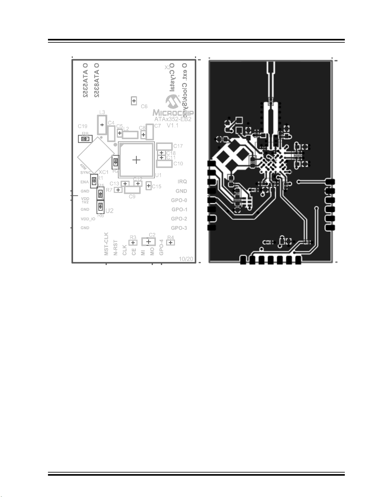
Figure 2-3. ATA8352 – Top Layer and Components
AN3770
ATA8352 Module
2. Place three vias below the ATA8352 device for the GND connection.
3. Place a short and straight connection for the RF path to the SMA connector and copy the 30 to 50Ω
conversion.
The following figure illustrates the module footprint.
© 2021 Microchip Technology Inc.
Application Note
DS00003770A-page 6
Microchip Confidential
Page 7

Figure 2-4. ATA8352 Module Footprint (dimension in mm)
AN3770
ATA8352 Module
2.3 Pin Details
The following table describes the ATA8352 module pin details. Refer to Figure 2-1 for the signal names.
Table 2-1. ATA8352 Module Pin Details
Name Description
ENA (Optional) Active high input to enable the DC/DC converter for 1.25V supply
GND GND connection
VDD_1V2 1.25V supply connection (use either external 1.25V supply or the on-module DCDC converter if
mounted. Do not use both supplies.)
GND GND connection
VDD_IO 3.3V IO supply connection
GND GND connection
MST-CLK 4 MHz master clock output from the ATA8352
N-RST Active low reset input signal for the ATA8352
SPI-CLK SPI clock input signal for the ATA8352
SPI-CE Active high SPI chip enable signal for the ATA8352
SPI-MISO SPI MISO input signal for the ATA8352
© 2021 Microchip Technology Inc.
Application Note
DS00003770A-page 7
Microchip Confidential
Page 8

...........continued
Name Description
SPI-MOSI SPI MOSl output signal from the ATA8352
GPO-4 GPO4 signal from the ATA8352
GPO-3 GPO3 signal from the ATA8352
GPO-2 GPO2 signal from the ATA8352
GPO-1 GPO1 signal from the ATA8352
GPO-0 GPO0 signal from the ATA8352
GND GND connection
IRQ Active high interrupt output from the ATA8352
48M 48 MHz input clock
RF SMA 50Ω antenna connector footprint
SYNC Synchronization input signal
AN3770
ATA8352 Module
2.4 Bill of Material
The following table provides the Bill of Material (BOM) for the ATA8352 module.
Table 2-2. ATA8352 Module BOM
Designator Description Quantity Value
C2 Ceramic capacitor, SMD 0402, X5R, 10V, 10% 1 1 µF
C4 Ceramic capacitor, SMD 0402, X7R, 16V, +/-10% (de19761) 1 1000 pF
C5 Ceramic capacitor, SMD 0201, C0G, 25V, +/-0.25pF 1 100 pF
C6 Ceramic Capacitor, KEMET CBR02C149B5GAC,
HF-Capacitor C0G / NP0, 1.4 pF, 50 V, HiQ-CBR, ± 0.1pF, 125 °C, SMD
0201
C6 (Alternative) Murata GCM0335C1E1R5CA16, AEC-Q200, HF-Capacitor C0G / NP0,
1.5 pF, 50 V, HiQ-CBR, ± 0.25pF, 125 °C, SMD 0201
C7 Ceramic capacitor, SMD 0402, X7R, 16V, +/-10% (de19761) 1 0.1 µF
C8 Ceramic capacitor, SMD 0201, C0G, 25V, +/-0.25pF 1 100 pF
C9 Ceramic capacitor, SMD 0402, X7R, 16V, +/-10% (de19761) 1 0.1 µF
C10 Ceramic capacitor, SMD 0402, X7R, 16V, +/-10% (de19761) 1 0.1 µF
C11 Ceramic capacitor, SMD 0201, C0G, 25V, +/-0.25pF 1 100 pF
C12 Ceramic capacitor, SMD 0201, C0G, 25V, +/-0.25pF 1 100 pF
1 1.4 pF
1 1.5 pF
C13 Ceramic capacitor, SMD 0201, C0G, 25V, +/-0.25pF 1 100 pF
C15 Ceramic capacitor, SMD 0201, C0G, 25V, +/-0.25pF 1 100 pF
C17 Ceramic capacitor, SMD 0402, X7R, 16V, +/-10% (de19761) 1 0.1 µF
C18 Ceramic capacitor, SMD 0201, C0G, 25V, +/-0.25pF 1 100 pF
C19 Ceramic capacitor, SMD 0402, X7R, 16V, +/-10% (de19761) 1 0.1 µF
© 2021 Microchip Technology Inc.
Application Note
DS00003770A-page 8
Microchip Confidential
Page 9

AN3770
ATA8352 Module
...........continued
Designator Description Quantity Value
L2 Chip inductor, SMD 0402, Murata LQW15AN3N3B80D, Fixed Inductors
Rdc = 30 mOhms , 3.3nH, Ir = 2000mA +/-0.1nH
L3 (Optional) Johanson Technology L-14C56NJV4T Inductor RF, 0603,
56NH,
5%
R3 RES 2.2 KΩ, 1/20W, 5%, 0201 SMD 1 47k
R4 RES 2.2 KΩ, 1/20W, 5%, 0201 SMD 1 47k
R7 Thick film resistor, SMD 0201, 1/20W, 5% 1 0R
U1 UWB TRX 1 ATA8352
X2 CONN SMA Jack R/A 500 Ω Edge MNT high frequency 26.5 GHz 1 901-10512-3
XC1 SMD crystal ECX-2236 series, 48 MHz
Refer to crystal specification in ATA8352 datasheet.
1 3.3 nH
1 BLM11B050A
1 48 MHz
© 2021 Microchip Technology Inc.
Application Note
DS00003770A-page 9
Microchip Confidential
Page 10

3. Current Consumption Profile
This chapter provides the ATA8352 module's current consumption profiles of the Prover and Verifier modes. The
measurement conditions are:
• t
• VDDIO = 3.0V
Note: The data sheet defines the electrical characteristics of the ATA8352 module's RF and IO pins. The 3.3V IO
supply provides voltage to the DC/DC converter on the module.
3.1 Supply Current Profile
The supply current profile for a complete Verifier operation including power-up, initialization, calibration of the Verifier
offset mode with Prover response and power-down is shown in Figure 3-1, Figure 3-2 and Figure 3-3. The figures
show the analog signals, VDD_CORE (supply voltage for the core), IDD_CORE (supply current for the core) at 1.25V
and IDD_SUP at 3.3V (supply domain), and the digital signals, N_RST, 1V2_ENA, SPI_CE, IRQ and Controller state
signals. The complete sequence of operations requires ~7.6 ms. The measurement was performed with the
evaluation kit using a SAMC21 MCU with 48 MHz clock and an SPI communication with an 8 MHz clock frequency.
The supply current (IDD_SUP) includes the current for the VDD_IO domain and the current for a DC/DC converter to
supply the VDD_CORE domain (the DC/DC converter used for the measurement is TPS62244-Q1 with a 1.25V
output voltage).
Following is the sequence operation:
1. The DC/DC is switched On at -7.1 ms when the signal, 1V2_ENA, is set to high and, after 1 ms, release the
2. Switch On the crystal oscillator at -5.8 ms.
3. Load the device registers.
4. Initialize the PLL at -3.7 ms and the calibration of the FLL RX at -3.2 ms.
5. Set the RF RX and TX frequencies at -1.7 ms, and enter the READY mode at -1.0 ms.
= 25°C
ambient
N_RST signal.
AN3770
Current Consumption Profile
3.2 Verifier Mode Current Consumption
The Verifier mode, VRo, is started with the transmission state and the controller state at 1101 (for details, refer to the
ATA8352 User Manual). See the following figure. The turnaround phases follow this and receive a locked state at
0110. The IRQ signal is activated when the receive is complete and the registers are read. Enable the reset signal
(N_RST) to start the power-down sequence and disable the DC/DC converter.
© 2021 Microchip Technology Inc.
Application Note
DS00003770A-page 10
Microchip Confidential
Page 11

Figure 3-1. Current Profile for Verifier Operation
AN3770
Current Consumption Profile
The following figure (zoomed in from -2.0 to 2.0 ms) shows the Verifier operation in VRo mode.
Figure 3-2. Current Profile for the Verifier Mode VRo
3.3 Prover Mode Current Consumption
When starting the Prover mode, the device switches to the RX mode to search for a preamble.
© 2021 Microchip Technology Inc.
Application Note
DS00003770A-page 11
Microchip Confidential
Page 12

AN3770
Current Consumption Profile
The following figure shows the Prover mode, PRo, where the initialization occurs similarly to the sequence in Figure
3-2. The Prover is operating in the Receiver Search mode as the controller state at 0101 indicates. When a valid
preamble and sync word are received, the Receiver Locked mode is entered as the controller state at 0110 shows.
When the data telegram is received, the turnaround sequence is executed and the Prover transmits the telegram, as
the controller state at 1101 shows. This sequence is completed with an IRQ and the activation of the Prover mode,
PRo, for the next data telegram.
Figure 3-3. Current Profile for the Prover Mode PRo
© 2021 Microchip Technology Inc.
Application Note
DS00003770A-page 12
Microchip Confidential
Page 13

4. RF Spectrum
The following figure shows the RF spectrum for the ATA8352 module for the composite signal (with low and high
modulation switched on).
Note: The RF filter is not used in the current version of the module, that is, the spectrum shown is the RF output
signal of the device with the default settings, fTX at 6.52 GHz.
Figure 4-1. RF Spectrum for Composite Signal
AN3770
RF Spectrum
© 2021 Microchip Technology Inc.
Application Note
DS00003770A-page 13
Microchip Confidential
Page 14

5. Document Revision History
Revision Date Section Description
A 01/2021 Document Initial Revision
AN3770
Document Revision History
© 2021 Microchip Technology Inc.
Application Note
DS00003770A-page 14
Microchip Confidential
Page 15

AN3770
The Microchip Website
Microchip provides online support via our website at www.microchip.com/. This website is used to make files and
information easily available to customers. Some of the content available includes:
• Product Support – Data sheets and errata, application notes and sample programs, design resources, user’s
guides and hardware support documents, latest software releases and archived software
• General Technical Support – Frequently Asked Questions (FAQs), technical support requests, online
discussion groups, Microchip design partner program member listing
• Business of Microchip – Product selector and ordering guides, latest Microchip press releases, listing of
seminars and events, listings of Microchip sales offices, distributors and factory representatives
Product Change Notification Service
Microchip’s product change notification service helps keep customers current on Microchip products. Subscribers will
receive email notification whenever there are changes, updates, revisions or errata related to a specified product
family or development tool of interest.
To register, go to www.microchip.com/pcn and follow the registration instructions.
Customer Support
Users of Microchip products can receive assistance through several channels:
• Distributor or Representative
• Local Sales Office
• Embedded Solutions Engineer (ESE)
• Technical Support
Customers should contact their distributor, representative or ESE for support. Local sales offices are also available to
help customers. A listing of sales offices and locations is included in this document.
Technical support is available through the website at: www.microchip.com/support
Microchip Devices Code Protection Feature
Note the following details of the code protection feature on Microchip devices:
• Microchip products meet the specifications contained in their particular Microchip Data Sheet.
• Microchip believes that its family of products is secure when used in the intended manner and under normal
conditions.
• There are dishonest and possibly illegal methods being used in attempts to breach the code protection features
of the Microchip devices. We believe that these methods require using the Microchip products in a manner
outside the operating specifications contained in Microchip’s Data Sheets. Attempts to breach these code
protection features, most likely, cannot be accomplished without violating Microchip’s intellectual property rights.
• Microchip is willing to work with any customer who is concerned about the integrity of its code.
• Neither Microchip nor any other semiconductor manufacturer can guarantee the security of its code. Code
protection does not mean that we are guaranteeing the product is “unbreakable.” Code protection is constantly
evolving. We at Microchip are committed to continuously improving the code protection features of our products.
Attempts to break Microchip’s code protection feature may be a violation of the Digital Millennium Copyright Act.
If such acts allow unauthorized access to your software or other copyrighted work, you may have a right to sue
for relief under that Act.
© 2021 Microchip Technology Inc.
Application Note
DS00003770A-page 15
Microchip Confidential
Page 16

AN3770
Legal Notice
Information contained in this publication is provided for the sole purpose of designing with and using Microchip
products. Information regarding device applications and the like is provided only for your convenience and may be
superseded by updates. It is your responsibility to ensure that your application meets with your specifications.
THIS INFORMATION IS PROVIDED BY MICROCHIP “AS IS”. MICROCHIP MAKES NO REPRESENTATIONS OR
WARRANTIES OF ANY KIND WHETHER EXPRESS OR IMPLIED, WRITTEN OR ORAL, STATUTORY OR
OTHERWISE, RELATED TO THE INFORMATION INCLUDING BUT NOT LIMITED TO ANY IMPLIED
WARRANTIES OF NON-INFRINGEMENT, MERCHANTABILITY, AND FITNESS FOR A PARTICULAR PURPOSE
OR WARRANTIES RELATED TO ITS CONDITION, QUALITY, OR PERFORMANCE.
IN NO EVENT WILL MICROCHIP BE LIABLE FOR ANY INDIRECT, SPECIAL, PUNITIVE, INCIDENTAL OR
CONSEQUENTIAL LOSS, DAMAGE, COST OR EXPENSE OF ANY KIND WHATSOEVER RELATED TO THE
INFORMATION OR ITS USE, HOWEVER CAUSED, EVEN IF MICROCHIP HAS BEEN ADVISED OF THE
POSSIBILITY OR THE DAMAGES ARE FORESEEABLE. TO THE FULLEST EXTENT ALLOWED BY LAW,
MICROCHIP'S TOTAL LIABILITY ON ALL CLAIMS IN ANY WAY RELATED TO THE INFORMATION OR ITS USE
WILL NOT EXCEED THE AMOUNT OF FEES, IF ANY, THAT YOU HAVE PAID DIRECTLY TO MICROCHIP FOR
THE INFORMATION. Use of Microchip devices in life support and/or safety applications is entirely at the buyer’s risk,
and the buyer agrees to defend, indemnify and hold harmless Microchip from any and all damages, claims, suits, or
expenses resulting from such use. No licenses are conveyed, implicitly or otherwise, under any Microchip intellectual
property rights unless otherwise stated.
Trademarks
The Microchip name and logo, the Microchip logo, Adaptec, AnyRate, AVR, AVR logo, AVR Freaks, BesTime,
BitCloud, chipKIT, chipKIT logo, CryptoMemory, CryptoRF, dsPIC, FlashFlex, flexPWR, HELDO, IGLOO, JukeBlox,
KeeLoq, Kleer, LANCheck, LinkMD, maXStylus, maXTouch, MediaLB, megaAVR, Microsemi, Microsemi logo, MOST,
MOST logo, MPLAB, OptoLyzer, PackeTime, PIC, picoPower, PICSTART, PIC32 logo, PolarFire, Prochip Designer,
QTouch, SAM-BA, SenGenuity, SpyNIC, SST, SST Logo, SuperFlash, Symmetricom, SyncServer, Tachyon,
TimeSource, tinyAVR, UNI/O, Vectron, and XMEGA are registered trademarks of Microchip Technology Incorporated
in the U.S.A. and other countries.
AgileSwitch, APT, ClockWorks, The Embedded Control Solutions Company, EtherSynch, FlashTec, Hyper Speed
Control, HyperLight Load, IntelliMOS, Libero, motorBench, mTouch, Powermite 3, Precision Edge, ProASIC, ProASIC
Plus, ProASIC Plus logo, Quiet-Wire, SmartFusion, SyncWorld, Temux, TimeCesium, TimeHub, TimePictra,
TimeProvider, WinPath, and ZL are registered trademarks of Microchip Technology Incorporated in the U.S.A.
Adjacent Key Suppression, AKS, Analog-for-the-Digital Age, Any Capacitor, AnyIn, AnyOut, Augmented Switching,
BlueSky, BodyCom, CodeGuard, CryptoAuthentication, CryptoAutomotive, CryptoCompanion, CryptoController,
dsPICDEM, dsPICDEM.net, Dynamic Average Matching, DAM, ECAN, Espresso T1S, EtherGREEN, IdealBridge, InCircuit Serial Programming, ICSP, INICnet, Intelligent Paralleling, Inter-Chip Connectivity, JitterBlocker, maxCrypto,
maxView, memBrain, Mindi, MiWi, MPASM, MPF, MPLAB Certified logo, MPLIB, MPLINK, MultiTRAK, NetDetach,
Omniscient Code Generation, PICDEM, PICDEM.net, PICkit, PICtail, PowerSmart, PureSilicon, QMatrix, REAL ICE,
Ripple Blocker, RTAX, RTG4, SAM-ICE, Serial Quad I/O, simpleMAP, SimpliPHY, SmartBuffer, SMART-I.S., storClad,
SQI, SuperSwitcher, SuperSwitcher II, Switchtec, SynchroPHY, Total Endurance, TSHARC, USBCheck, VariSense,
VectorBlox, VeriPHY, ViewSpan, WiperLock, XpressConnect, and ZENA are trademarks of Microchip Technology
Incorporated in the U.S.A. and other countries.
SQTP is a service mark of Microchip Technology Incorporated in the U.S.A.
The Adaptec logo, Frequency on Demand, Silicon Storage Technology, and Symmcom are registered trademarks of
Microchip Technology Inc. in other countries.
GestIC is a registered trademark of Microchip Technology Germany II GmbH & Co. KG, a subsidiary of Microchip
Technology Inc., in other countries.
All other trademarks mentioned herein are property of their respective companies.
©
2021, Microchip Technology Incorporated, Printed in the U.S.A., All Rights Reserved.
ISBN: 978-1-5224-7312-1
© 2021 Microchip Technology Inc.
Application Note
DS00003770A-page 16
Microchip Confidential
Page 17

AN3770
Quality Management System
For information regarding Microchip’s Quality Management Systems, please visit www.microchip.com/quality.
© 2021 Microchip Technology Inc.
Application Note
DS00003770A-page 17
Microchip Confidential
Page 18

Worldwide Sales and Service
AMERICAS ASIA/PACIFIC ASIA/PACIFIC EUROPE
Corporate Office
2355 West Chandler Blvd.
Chandler, AZ 85224-6199
Tel: 480-792-7200
Fax: 480-792-7277
Technical Support:
www.microchip.com/support
Web Address:
www.microchip.com
Atlanta
Duluth, GA
Tel: 678-957-9614
Fax: 678-957-1455
Austin, TX
Tel: 512-257-3370
Boston
Westborough, MA
Tel: 774-760-0087
Fax: 774-760-0088
Chicago
Itasca, IL
Tel: 630-285-0071
Fax: 630-285-0075
Dallas
Addison, TX
Tel: 972-818-7423
Fax: 972-818-2924
Detroit
Novi, MI
Tel: 248-848-4000
Houston, TX
Tel: 281-894-5983
Indianapolis
Noblesville, IN
Tel: 317-773-8323
Fax: 317-773-5453
Tel: 317-536-2380
Los Angeles
Mission Viejo, CA
Tel: 949-462-9523
Fax: 949-462-9608
Tel: 951-273-7800
Raleigh, NC
Tel: 919-844-7510
New York, NY
Tel: 631-435-6000
San Jose, CA
Tel: 408-735-9110
Tel: 408-436-4270
Canada - Toronto
Tel: 905-695-1980
Fax: 905-695-2078
Australia - Sydney
Tel: 61-2-9868-6733
China - Beijing
Tel: 86-10-8569-7000
China - Chengdu
Tel: 86-28-8665-5511
China - Chongqing
Tel: 86-23-8980-9588
China - Dongguan
Tel: 86-769-8702-9880
China - Guangzhou
Tel: 86-20-8755-8029
China - Hangzhou
Tel: 86-571-8792-8115
China - Hong Kong SAR
Tel: 852-2943-5100
China - Nanjing
Tel: 86-25-8473-2460
China - Qingdao
Tel: 86-532-8502-7355
China - Shanghai
Tel: 86-21-3326-8000
China - Shenyang
Tel: 86-24-2334-2829
China - Shenzhen
Tel: 86-755-8864-2200
China - Suzhou
Tel: 86-186-6233-1526
China - Wuhan
Tel: 86-27-5980-5300
China - Xian
Tel: 86-29-8833-7252
China - Xiamen
Tel: 86-592-2388138
China - Zhuhai
Tel: 86-756-3210040
India - Bangalore
Tel: 91-80-3090-4444
India - New Delhi
Tel: 91-11-4160-8631
India - Pune
Tel: 91-20-4121-0141
Japan - Osaka
Tel: 81-6-6152-7160
Japan - Tokyo
Tel: 81-3-6880- 3770
Korea - Daegu
Tel: 82-53-744-4301
Korea - Seoul
Tel: 82-2-554-7200
Malaysia - Kuala Lumpur
Tel: 60-3-7651-7906
Malaysia - Penang
Tel: 60-4-227-8870
Philippines - Manila
Tel: 63-2-634-9065
Singapore
Tel: 65-6334-8870
Taiwan - Hsin Chu
Tel: 886-3-577-8366
Taiwan - Kaohsiung
Tel: 886-7-213-7830
Taiwan - Taipei
Tel: 886-2-2508-8600
Thailand - Bangkok
Tel: 66-2-694-1351
Vietnam - Ho Chi Minh
Tel: 84-28-5448-2100
Austria - Wels
Tel: 43-7242-2244-39
Fax: 43-7242-2244-393
Denmark - Copenhagen
Tel: 45-4485-5910
Fax: 45-4485-2829
Finland - Espoo
Tel: 358-9-4520-820
France - Paris
Tel: 33-1-69-53-63-20
Fax: 33-1-69-30-90-79
Germany - Garching
Tel: 49-8931-9700
Germany - Haan
Tel: 49-2129-3766400
Germany - Heilbronn
Tel: 49-7131-72400
Germany - Karlsruhe
Tel: 49-721-625370
Germany - Munich
Tel: 49-89-627-144-0
Fax: 49-89-627-144-44
Germany - Rosenheim
Tel: 49-8031-354-560
Israel - Ra’anana
Tel: 972-9-744-7705
Italy - Milan
Tel: 39-0331-742611
Fax: 39-0331-466781
Italy - Padova
Tel: 39-049-7625286
Netherlands - Drunen
Tel: 31-416-690399
Fax: 31-416-690340
Norway - Trondheim
Tel: 47-72884388
Poland - Warsaw
Tel: 48-22-3325737
Romania - Bucharest
Tel: 40-21-407-87-50
Spain - Madrid
Tel: 34-91-708-08-90
Fax: 34-91-708-08-91
Sweden - Gothenberg
Tel: 46-31-704-60-40
Sweden - Stockholm
Tel: 46-8-5090-4654
UK - Wokingham
Tel: 44-118-921-5800
Fax: 44-118-921-5820
© 2021 Microchip Technology Inc.
Application Note
DS00003770A-page 18
 Loading...