

Page 1
AN851
A FLASH Bootloader for PIC16 and PIC18 Devices
Author: Ross M. Fosler and
Rodger Richey
Microchip Technology Inc.
INTRODUCTION
Among the many features built into Microchip’s
Enhanced FLASH Microcontroller devices is the capability of the program memory to self-program. This very
useful feature has been deliberately included to give
the user the ability to perform bootloading operations.
Devices like the PIC18F452 are designed with a designated “boot block”, a small section of protectable program memory allocated specifically for bootload
firmware.
This application note demonstrates a very powerful
bootloader implementation for the PIC16F87XA and
PIC18F families of microcontrollers. The coding for the
two device families is slightly different; however, the
functionality is essentially the same. The goals of this
implementation stress a maximum performance and
functionality, while requiring a minimum of code space.
FIRMWARE
Basic Operation
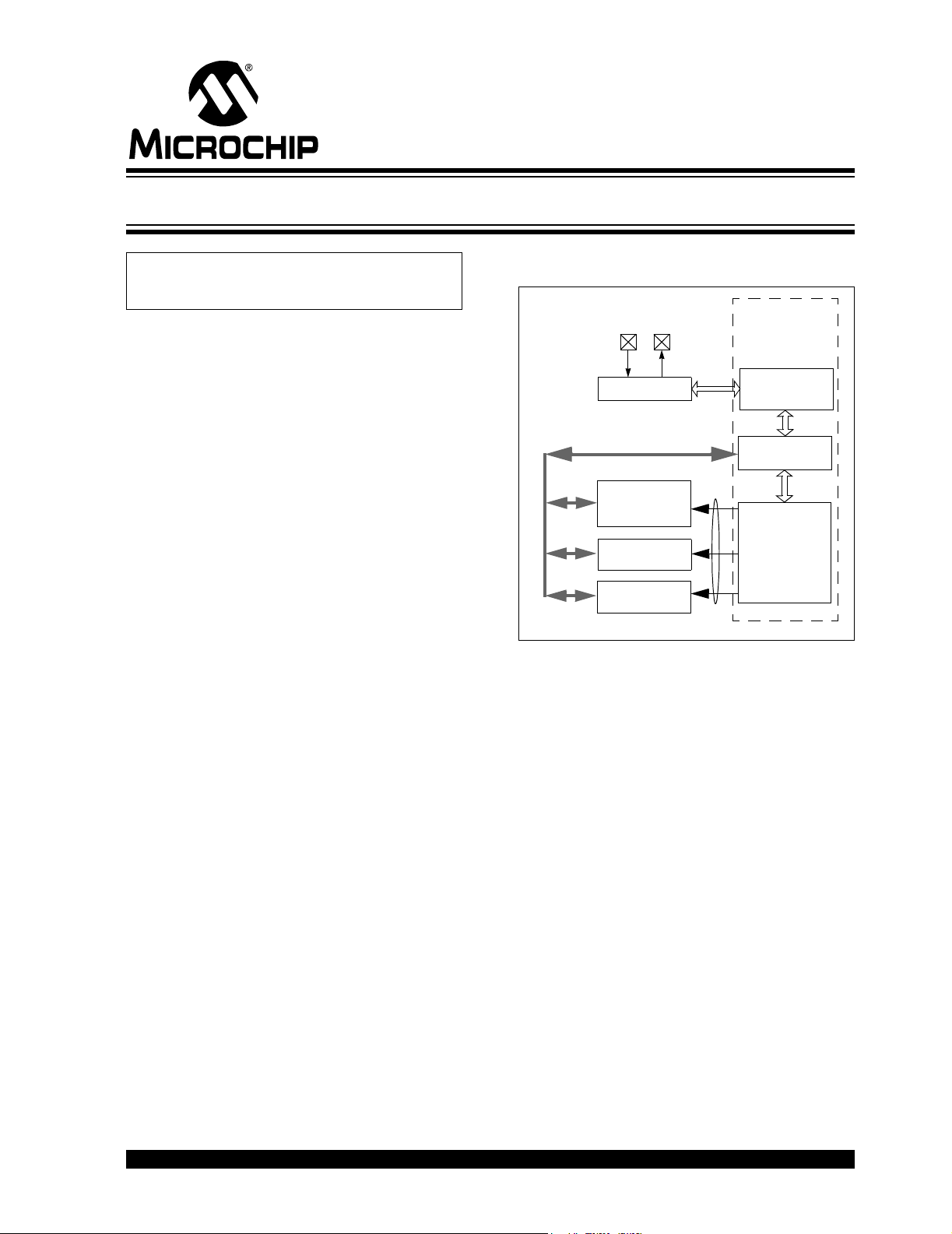
Figure 1 summarizes the essential firmware design of
the bootloader. Data is received through the USART
module, configured in Asynchronous mode for compatibility with RS-232 and passed through the
transmit/receive engine. The engine filters and parses
the data, storing the information into a data buffer in
RAM. The command interpreter evaluates the command information within the buffer to determine what
should be done (i.e., Is the data written into a memory
unit? Is data read from a memory unit? Does the firmware version need to be read?). Once the operation is
performed, data is passed back to the transmit/receive
engine to be transmitted back to the source, closing the
software flow control loop.
FIGURE 1: BOOTLOADER FUNCTIONAL
BLOCK DIAGRAM
Bootloader
TXRX
USART
FLASH
Program
Memory
Data Bus
EE
Data
Memory
Configuration
Registers
Control
Firmware
Transmit/Receive
Engine
RAM
Buffer
Command
Interpreter
COMMUNICATIONS
The microcontroller’s USART module is used to
receive and transmit data; it is configured as a UART to
be compatible with RS-232 communications. The
device can be set up in an application to bootload from
a computer through its standard serial interface. The
following communications settings are used:
• 8 data bits
•No parity
•1 STOP bit
The baud rate setting is variable depending on the
application. Baud rate selection is discussed later.
ã 2002 Microchip Technology Inc. DS00851B-page 1
Page 2

AN851
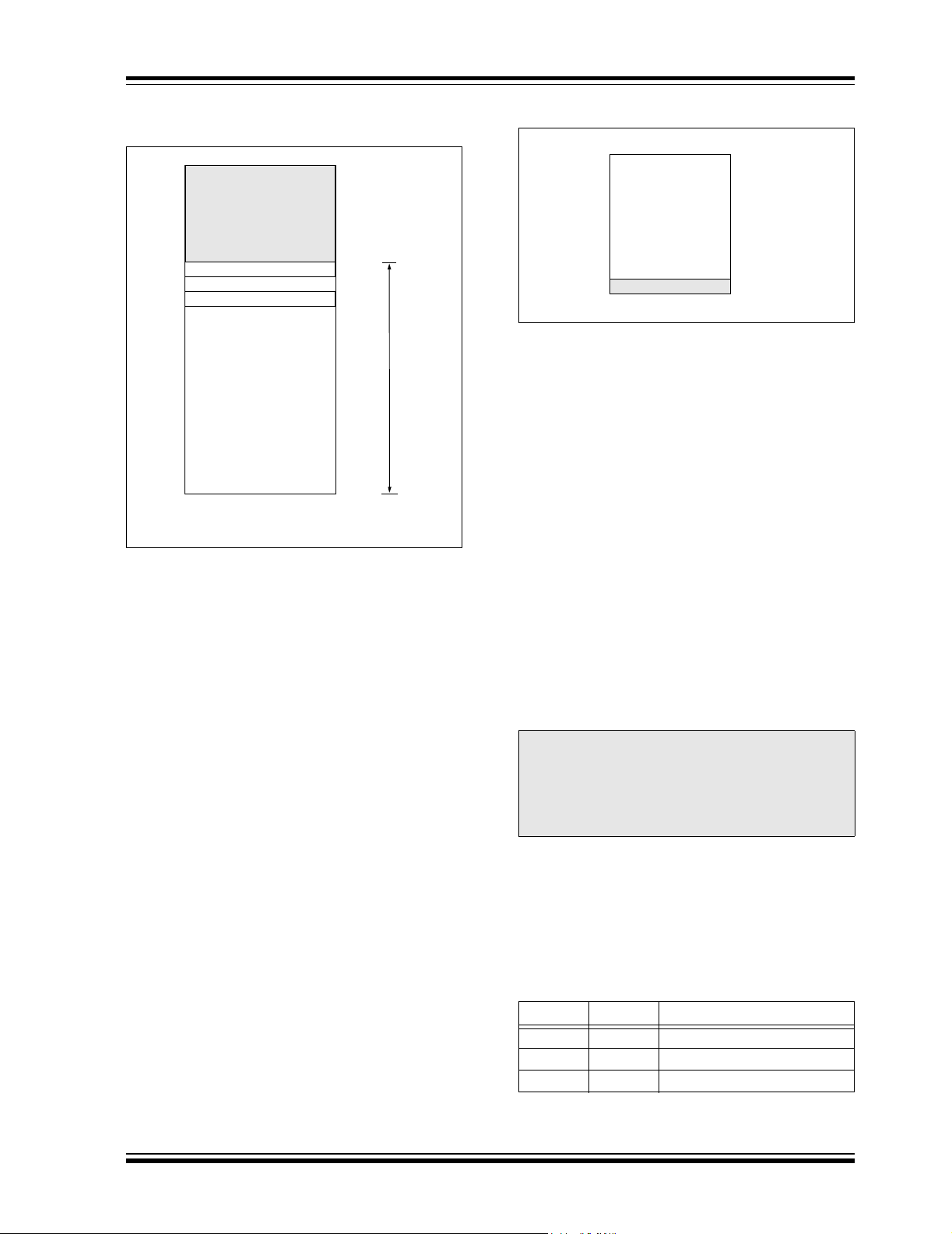
THE RECEIVE/TRANSMIT BUFFER
All data is moved through a buffer (referred to as the
Receive/Transmit Buffer). The buffer is a maximum of
255 bytes deep. This is the maximum packet length
supported by the protocol. However, some devices
may not support the largest packet size due to memory
limitations. Figure 2 shows an example of the mapping
of the buffer within the PIC18F452.
Note: The actual packet length supported by a
particular device depends on the size of its
data memory.
A useful feature of the receive/transmit buffer is that it
retains its memory between packets, thus allowing very
fast repeat and replication operations. That is, if an
empty packet is sent, the data currently in memory will
be executed as if it were just received.
FIGURE 2: DATA MEMORY USAGE ON
THE PIC18F452
Bootloader
Work Area
Receive/Transmit
Buffer
000h
008h
Memory Organization
PROGRAM MEMORY USAGE
Currently, PIC18F devices reserve the first 512 bytes of
Program Memory as the boot block. Future devices
may expand this, depending on application requirements for these devices. However, this bootloader is
designed to occupy the current designated boot block
of 512 bytes (or 256 words) of memory. Figure 3 shows
a memory map of the PIC18F452. The boot area can
be code protected to prevent accidental overwriting of
the boot program.
FIGURE 3: PROGRAM MEMORY MAP OF
THE PIC18F452
Boot Program
RESET Vector
High Priority Interrupt Vector
Low Priority Interrupt Vector
0200h
0208h
0218h
107h
Unused
SFRs
FFFh
COMMAND INTERPRETER
The command interpreter decodes and executes ten
different commands, seven base commands and three
special commands. A complete list of the commands is
provided in Appendix A. The base commands allow for
read, write, and erase operations on all types of
non-volatile memory. The other three commands are for
special operations, such as repeating the last
command, replicating the data, and resetting the device.
Note that the PIC18F devices have greater access to,
and control of, memory than PIC16F devices. For
example, PIC16F devices do not have access to the
configuration memory, thus they do not use the configuration commands. Therefore, not all instructions are
available in the PIC16F bootloader.
Program Memory
User Memory Space
7FFFh
Note: Memory areas not shown to scale.
PIC16F87XA enhanced microcontrollers are designed
to use the first 256 words of program memory. Figure 4
shows the memory map of the PIC16F877A. Like the
PIC18F452 and other PIC18F devices, the boot area
can be write protected to prevent accidental overwriting
of the boot program.
DS00851B-page 2 ã 2002 Microchip Technology Inc.
Page 3
AN851
FIGURE 4: PROGRAM MEMORY MAP OF
THE PIC16F877A
Boot Program
RESET Vector
Interrupt Vector
Program Memory
Note: Memory areas not shown to scale.
0100h
0104h
User Memory Space
3FFFh
REMAPPED VECTORS
Since the hardware RESET and interrupt vectors lie
within the boot area and cannot be edited if the block is
protected, they are remapped through software to the
nearest parallel location outside the boot block.
Remapping is simply a branch for interrupts, so PIC18F
users should note an additional latency of 2 instruction
cycles to handle interrupts. Upon RESET, there are
some boot condition checks, so the RESET latency is
an additional 10 instruction cycles (as seen in the
example source code).
For PIC16F87XA devices, the interrupt latency is an
additional 9 instruction cycles on top of the 3 to 4 normally experienced; the RESET latency is 18 instruction
cycles. This additional latency comes from saving
device context data in shared memory. The example
code uses locations 7Dh, 7Eh, and 7Fh to store the
PCLATH, STATUS, and W registers, respectively. The
source code can be changed, but the saved data must
remain in the shared memory area.
DATA MEMORY USAGE
The last location in data memory of the device
(Figure 5) is reserved as a non-volatile Boot mode flag.
This location contains FFh by default, which indicates
Boot mode. Any other value in this location indicates
normal Execution mode.
FIGURE 5: DATA MEMORY MAP
000h
EE Data
Memory
Boot Control Byte
XXXh
Communication Protocol
The bootloader employs a basic communication
protocol that is robust, simple to use, and easy to
implement.
PACKET FORMAT
All data that is transmitted to or from the device follows
the basic packet format:
<STX><STX>[<DATA><DATA>...]<CHKSUM><ETX>
where each <...> represents a byte and [...]
represents the data field.
The start of a packet is indicated by two ‘Start of TeXt’
control characters (<STX>), and is terminated by a single ‘End of TeXt’ control character (<ETX>). The last
byte before the <ETX> is always a checksum, which is
the two’s complement of the Least Significant Byte of
the sum of all data bytes.
The data field is limited to 255 data bytes. If more bytes
are received, then the packet is ignored until the next
<STX> pair is received.
Note: Although the protocol supports 255 bytes of
data, the specific device that contains the
bootloader firmware may have a sufficiently
large data memory to support the largest
packet size. Refer to the data sheet for the
particular device for more information.
CONTROL CHARACTERS
There are three control characters that have special
meaning. Two of them, <STX> and <ETX>, are introduced above. The last character not shown is the ‘Data
Link Escape’, <DLE>. Table 1 provides a summary of
the three control characters.
TABLE 1: CONTROL CHARACTERS
Control Value Description
<STX> 0Fh Start of TeXt
<ETX> 04h End of TeXt
<DLE> 05h Data Link Escape
ã 2002 Microchip Technology Inc. DS00851B-page 3
Page 4
AN851
The <DLE> is used to identify a value that could be
interpreted in the data field as a control character.
Within the data field, the bootloader will always accept
the byte following a <DLE> as data, and will always
send a <DLE> before any of the three control characters. For example, if a byte of value 0Fh is transmitted
as part of the data field, rather than as the <STX> con-
trol character, the <DLE> character is inserted before
the <STX>. This is called “byte stuffing”.
Note: Control characters are not considered data
and are not included in the checksum.
COMMANDS
The data field for each packet contains one command
and its associated data. The commands are detailed in
Appendix A.
COMMAND RESPONSE LATENCY
Flow control is built into the protocol. Thus, for every
received command (except RESET), there is a
response. If there is no response, then one (or more) of
the following has happened:
• the data was corrupted (bad checksum)
• the packet was never received
• the data field was too long
• RESET was executed
So how long do you wait before deciding a problem has
occurred? The response latency (shown in Figure 6) is
dependent on the amount of data sent, the command
being executed, and the clock frequency.
For read commands, the latency is highly dependent
on the clock frequency, and the size of the packet. For
a small packet at high frequency, the response is
almost immediate, typically on the order of a few microseconds. For large packets, the latency could be on the
order of hundreds of microseconds.
In general, read commands require very little time compared to write commands. Write commands are mostly
dependent on internally timed write cycles. For example, the typical write time required for a single
EEPROM location is 4 ms. If the maximum packet size
(250 bytes of writable data) was sent, the receive to
transmit latency would be about 1 second.
FIGURE 6: RECEIVE TO TRANSMIT
LATENCY
RX
TX
Delay
Automatic Baud Rate Detection
The bootloader is provided with an automatic baud rate
detection algorithm that will detect most baud rates for
most input clock frequencies (F
determines the best value for the Baud Rate Generator
and then loads the SPBRG register on the
microcontroller with the determined value.
Note: Refer to the specific device data sheet for
information about the USART module and
its associated registers.
OSC). The algorithm
SYNCHRONIZING
The first <STX> in the protocol is the synchronization
byte. It is used to match the device’s baud rate to the
source’s baud rate. Thus, the device is synchronized to
the source on every new packet.
Note: If a ‘Start of TeXt’ condition is received
during the reception of a packet, then no
synchronization occurs.
SELECTING FOSC AND BAUD RATE
The recommended baud rate for this application is
9600 bps. This is the ideal rate for a device operating
from 4 MHz, to the device’s maximum operating frequency (40 MHz in most cases). Higher baud rates are
possible, but degenerate conditions can occur.
There are a few clock frequency/standard baud rate
combinations that lead to a degenerate baud rate
selection during synchronization; under such conditions, the device will never synchronize to the source.
Clock frequencies that avoid such degenerate
conditions are given by the equation:
FOSC = (1 ± E)(X + 1)(16)(B)
where E is the error (typically 2%), X is the value for the
SPBRG register, and B is the baud rate. A table of calculated clock oscillator ranges for most of the common
baud rates is provided in Appendix B for quick
reference.
BOOTING A DEVICE
Entering and Leaving Boot Mode
With the bootloader firmware loaded, there are two distinct modes of operation: Boot Mode and User Mode.
The bootloader uses the last location of data memory
to determine which mode to run in. A value of FFh indicates Boot mode. Any other value indicates User
mode. Thus, a new part with its data memory not
initialized will automatically enter Boot mode the first
time.
DS00851B-page 4 ã 2002 Microchip Technology Inc.
Page 5

AN851
To leave Boot mode, the last location must be changed
to some value other than FFh. Then, a device RESET
(hardware or software) is initiated. For PIC18F devices,
the RESET command actually generates a true RESET
via the RESET instruction (same as MCLR
tying a port pin to MCLR
in firmware on PIC16F87XA devices. Although the
RESET command is supported, it only causes the
PIC16F device to jump to the RESET vector; the registers used to perform bootload operations are not
changed to their RESET states.
, a true RESET is not possible
). Other than
Reading/Writing/Erasing Program Memory
PIC18F
For the PIC18F devices, commands 1 through 3 support operations to FLASH program memory. Read
operations occur at the byte level. Write operations are
performed on multiples of 8 bytes (one block). Erase
operations are performed on 64 bytes (one row).
When writing program memory on a PIC18F device,
the memory should be erased. The default operation is:
bits can only be cleared when written to. An erase operation is the only action that can be used to set bits in
program memory. Thus, if the bootloader protection
bits are not setup in the configuration bytes, operations
on memory from 000h to 1FFh could partially, or
completely disable the bootloader firmware.
User IDs (starting at address 200000h) are considered
to be part of program memory and are written and
erased like normal FLASH program memory. The
Device ID (addresses 3FFFFEh and 3FFFFFh) is also
considered program memory. While they can be
accessed, however, they are read only and cannot be
altered.
PIC16F
The PIC16F87XA devices support reading and writing
to program memory. Commands 1 and 2 support operations to FLASH program memory. Read operations
occur at the word level (2 bytes). Write operations are
performed on multiples of 4 words (8 bytes). Since
write operations are erase-before-write, the erase command is not supported. The bootloader area, from 000h
to 0FFh, should be write protected to prevent
overwriting itself.
Neither the User ID nor the Device ID locations are
accessible during normal operation on the PIC16 architecture; therefore, these areas can neither be read nor
written.
Reading/Writing Data Memory
Data memory is read or written one byte at a time,
through commands 4 and 5. Since it is not actually
mapped to the normal FLASH memory space, the
address starts at 000h and continues to the end of
EEDATA memory.
Note that the last location of the data memory is used
as a boot flag. Writing anything other than FFh to the
last location indicates normal code execution.
Configuration Bits
PIC18F
PIC18F devices allow access to the device configuration bits (addresses starting at 300000h) during normal
operation. In the bootloader, commands 6 and 7 provide this access. Data is read one byte at a time and,
unlike program memory, is written one byte at a time.
Since configuration bits are automatically erased
before being written, there is no erase command for
configuration memory.
Having access to configuration settings is very powerful; it is also potentially very dangerous. For example,
assume that the system is designed to run in HS mode,
with a 20 MHz crystal. If the bootloader changes the
oscillator setting to LP mode, the system will cease to
function — including the bootloader! Basically, the
system has been killed by improperly changing one bit.
It is also important to note some configuration bits are
single direction bits in Normal mode; they can only be
changed to one state, and cannot be changed back.
The code protection bits in Configuration Registers 5L
and 5H are a good example. If any type of code protection is enabled for a block, it cannot be disabled without
a device programmer. Essentially, the bootloader
cannot reverse code protection.
PIC16F
The configuration memory is not accessible during normal operation on the PIC16 architecture; therefore, this
area can neither be read nor written.
ã 2002 Microchip Technology Inc. DS00851B-page 5
Page 6

AN851
WRITING CODE
The bootloader operates as a separate entity, which
means that an application can be developed with very
little concern about what the bootloader is doing. This
is as it should be; the bootloader should be dormant
code until an event initiates a boot operation. Under
ideal circumstances, bootloader code should never be
running during an application’s intended normal
operation.
When developing an application with a resident
bootloader, some basic principles must be kept in
mind:
Writing in Assembly
When writing in assembly, the boot block and new vectors must be considered. For modular code, this is generally just a matter of changing the linker script file for
the project. An example is given in Appendix D. If an
absolute address is assigned to a code section, the
address must point somewhere above the boot block.
For those who write absolute assembly, all that is necessary is to remember that for PIC18F devices, the
new RESET vector is at 200h, and the interrupt vectors
are at 208h and 218h. For PIC16F87XA devices, the
RESET vector is at 100h and the interrupt vector is at
104h. No code, except the bootloader, should reside in
the boot block.
Writing in C
When using the MPLAB® C18 C compiler to develop
PIC18F firmware for an application, the standard
start-up object (c018.o or c018i.o) must be rebuilt
with the new RESET vector. Like modular assembly,
the linker file must be changed to incorporate the protected boot block and new vectors. Appendix D shows
an example linker file.
For users of other compilers, for either PIC16F87XA or
PIC18F devices, check with the compiler’s software
user guide to determine how to change the start-up
code and vectors.
Bootloader Re-Entry
If the need exists to re-enter Boot mode from the application (and it usually does), the last location of the data
memory must be set to FFh. The code in Example 1
demonstrates how this might be done in an application
on a PIC18F device. Since the bootloader assumes
RESET conditions, a RESET instruction should be
initiated after setting the last location.
EXAMPLE 1: SETTING THE LAST
LOCATION OF THE DATA
MEMORY
setf EEADR ; Point to the last byte
setf EEADRH
setf EEDATA ; Bootmode control byte
movlw b'00000100 ; Setup for EEData
movwf EECON1
movlw 0x55 ; Unlock
movwf EECON2
movlw 0xAA
movwf EECON2
bsf EECON1, WR ; Start the write
nop
btfsc EECON1, WR ; Wait
bra $ - 2
reset
Debugging
For most situations, it is not necessary to have the
bootloader firmware in memory to do debugging of an
application with either the MPLAB ICD 2 or ICE
devices. However, branch statements must be inserted
at the hardware vectors to get to the new designated
vectors. It may also be useful to have the start-up timing match exactly to the bootloader entry. When development of the application is finished, either remove the
branches and rebuild the project, or export only the
memory above the boot block. This code can then be
distributed to those who are updating their firmware.
DS00851B-page 6 ã 2002 Microchip Technology Inc.
Page 7
AN851
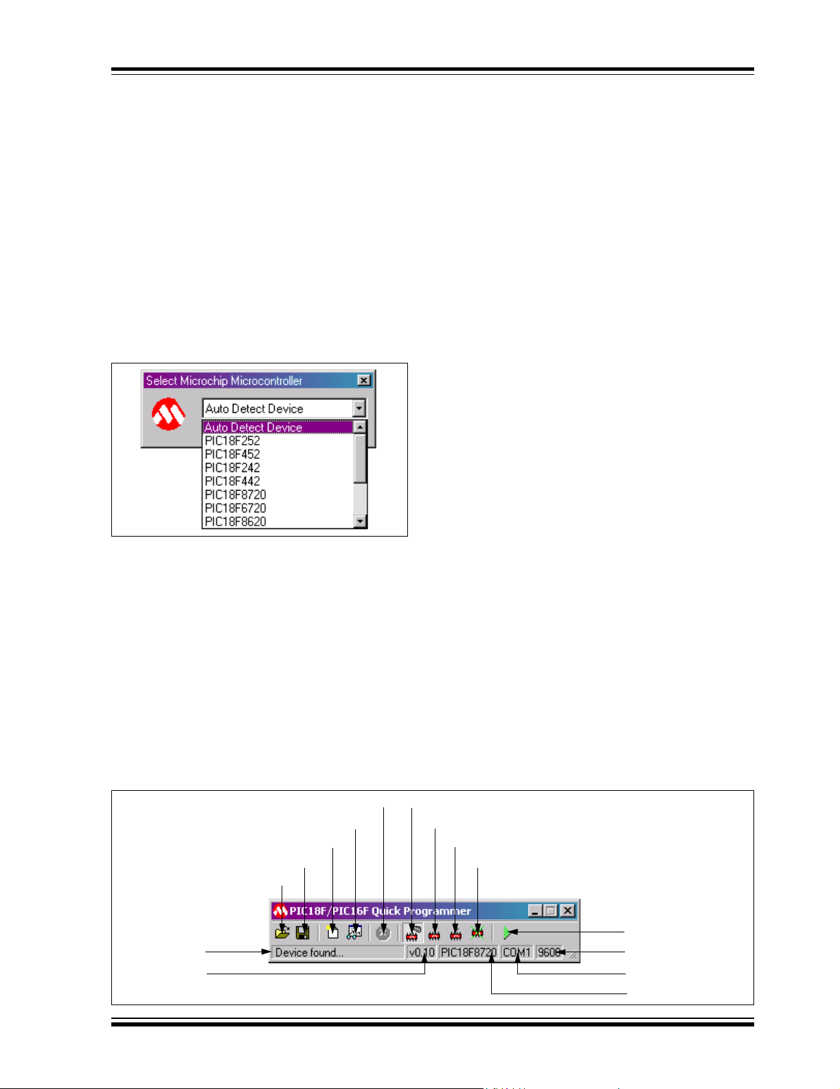
EXAMPLE SOFTWARE
The Microchip PIC16/PIC18 Quick Programmer is a
simple application designed to run on IBM
desktop computers; it is provided with the FLASH bootloader to perform basic programming operations. The
Quick Programmer should be used as a starting point
for users to create their own programming applications.
Selecting a Device
The first thing to appear after launching P1618QP.EXE
is the device selection dialog box (Figure 7). This floating box gives the user the option to manually select a
device to communicate with, from a drop-down menu.
For PIC18F devices, the automatic detection feature is
available. PIC16F devices must be manually selected.
FIGURE 7: DEVICE SELECTION
The Main Toolbar
The main program menu (Figure 8) appears as a floating toolbar over any other running applications, and not
as its own window. It provides some basic commands,
as well as information from the device.
CONNECTING TO A DEVICE
Before anything can happen, communications to the
attached device must be opened. This is done with the
Connect to Device button. If automatic detection was
selected, then the software will read the device ID and
try to match it with device information provided in the
P1618QP.INI. If a device is manually selected, then
®
compatible
the settings for that particular device are forced. In
either event, the device identity is shown in the Device
Identifier area.
Note that PIC16F devices cannot access device ID
memory during normal execution; thus, PIC16F
devices must be manually selected.
READING/WRITING/ERASING
The Read Device, Write To Device and Erase Device
buttons are used for reading, writing, and erasing the
attached device. The Read Device button tells the program to read the entire device. The Write to Device button writes only the data imported from a HEX file. The
Erase Device button erases the entire device; the
command is not available for PIC16F devices.
IMPORTING/EXPORTING HEX FILES
Basic file import and export operations are available.
The Microchip PIC16/PIC18 Quick Programmer uses
formatted text files to store data, rather than large
chunks of memory. Importing converts the HEX file into
a formatted text file; exporting does the opposite. The
program uses the formatted text file for storage and
display.
When importing a file, always be certain that the HEX
file is padded and aligned to a 16-byte boundary.
MPLAB IDE automatically pads to 16 bytes when an
integer multiple of 16 bytes of data is selected on a
16-byte boundary when using the Export feature.
VIEWING/CLEARING MEMORY
The View Data and Clear Data buttons allow the user
to view or clear the data that was imported, or read from
the device. The program does not include any type of
text viewer, and uses the viewer specified in the
PIC1618QP.INI file. By default, the viewer used in
Windows
®
is Notepad.
RUN MODE
When the desired data is loaded onto the device,
selecting this button will put the device into User mode,
by writing 00h to the last location of the data memory.
FIGURE 8: QUICK PROGRAMMER TOOL BAR
End Current Operation
View Imported File
Clear Imported File from Memory
Export HEX File
Import HEX File
Status Message
Revision Level
ã 2002 Microchip Technology Inc. DS00851B-page 7
Connect to Device
Read Program Memory
Write to Program Memory
Erase Device
Run Program on Device
Baud Rate Identifier
Port Identifier
Device Identifier
Page 8
AN851
PORT AND BAUD RATE SELECTION
The default serial port and its baud rate (COM1, 9600)
are specified in the PIC1618QP.INI file. The user
may change these settings while the application is running by right-click on either the port, or baud rate identifier. A menu of valid options that the user may select
from (COM ports or baud rates) will appear.
Menu Options
Right-clicking on the status or the toolbar displays a
pop-up menu that gives access to some settings and
advanced operations. Figure 9 shows the menu
options available.
FIGURE 9: MENU OPTIONS
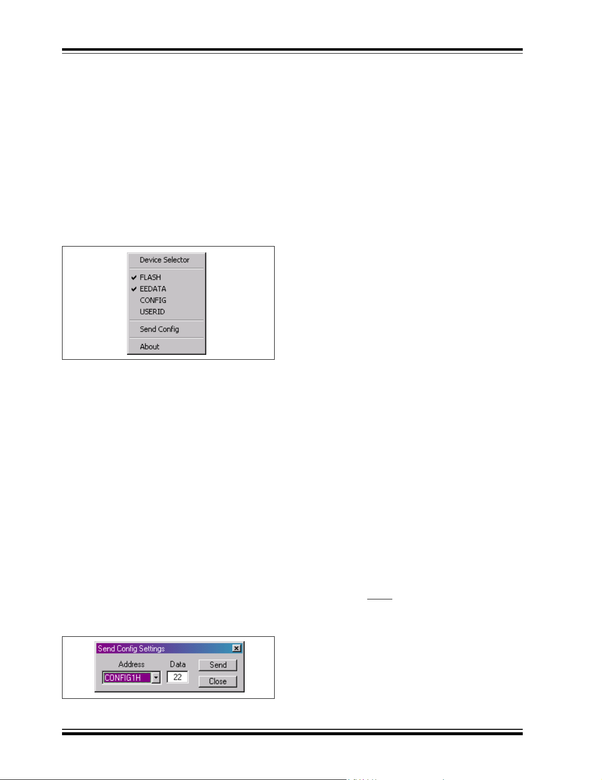
DEVICE SELECTOR
This menu option gives the user the ability to re-select
a device, or select a new device (see “Selecting a
Device” and Figure 7).
MEMORY ACCESS
The memory types are either checked or unchecked to
determine access. As an example, Figure 9 shows
access to FLASH program memory and data memory,
while access to CONFIG memory and User ID memory
is ignored. Since normal access to CONFIG and User
ID memory is not allowed in PIC16F devices, these
options are not available when a PIC16F device is
selected.
SEND CONFIG
The check access for CONFIG in Figure 9 is for read
operations only, due to the danger imposed by writing
all configuration bits sequentially. The “Send Config
Settings” dialog box (Figure 10) is used to actually write
configuration register settings.
FIGURE 10: SETTING CONFIG BITS
Selecting a configuration register label from the
Address list box will automatically load the current data
at that address. The value in the Data field can be
edited, then written back to the device by clicking on
the Send button.
DIFFERENCES BETWEEN THE PIC16F87XA AND PIC18F BOOTLOADERS
Because of architectural enhancements in PIC18F
devices, there are two main differences between the
PIC16F87XA and PIC18F bootloaders.
1. The PIC16F87XA bootloader does not support
the following commands:
• Erase FLASH
• Read CONFIG
• Write CONFIG
2. The RESET command is only partially supported. When the microcontroller receives a
RESET command, it executes a goto 0x0000.
This is not a true RESET of the microcontroller.
The following registers are not set to their
default RESET states on execution of the
command:
• EEADR
• EEADRH
• EECON1
• OPTION_REG
• RCSTA
•STATUS
• TXSTA
• EEDATA
• EEDATH
•FSR
•PIR1
• SPBRG
•TRISC
This is particularly important when leaving Boot
mode via a software RESET. The application software must be prepared to accept non RESET values in the registers listed above. If RESET
conditions are necessary, then the listed registers
should be initialized in the application code. The
alternative is to always perform a hardware
RESET (MCLR
operation.
) after completing a bootload
DS00851B-page 8 ã 2002 Microchip Technology Inc.
Page 9

APPENDIX A: BOOTLOADER COMMANDS
TABLE A-1: BOOTLOADER COMMANDS
AN851
Name Number Description
RESET ANY Reset the Device [<COM><0x00>] none XX
RD_VER 00h Read Bootloader
Version Information
RD_FLASH 01h Read <LEN> bytes
from Program
Memory
WT_FLASH 02h Write <LEN> blocks to
Program Memory
ER_FLASH 03h Erase <LEN> rows of
Program Memory
RD_EEDATA 04h Read <LEN> bytes
from EE Data Memory
WT_EEDATA05h Write <LEN> bytes to
EE Data Memory
RD_CONFIG 06h Read <LEN> bytes
from Configuration
Memory
WT_CONFIG 07h Write <LEN> bytes to
Configuration Memory
REPEAT COM Repeat last Command [Empty data field] Refer to the appropriate
REPLICATE COM Write old Buffer Data
to another area
Command Device
[data field]
[<0x00><0x02>] [<0x00><0x02><VERL
[<0x01><LEN><ADDRL
><ADDRH><ADDRU>]
[<0x02><LEN><ADDRL
><ADDRH><ADDRU>...
LEN bytes of Data
...]
[<0x03><LEN><ADDRL
><ADDRH><ADDRU>]
[<0x04><LEN><ADDRL
><ADDRH><0x00>]
[<0x05><LEN><ADDRL
><ADDRH><0x00>...
LEN bytes of Data
...]
[<0x06><LEN><ADDRL
><0x00><0x30>]
[<0x07><LEN><ADDRL
><0x00><0x30>...
LEN bytes of Data
...]
[<COM><LEN><ADDRL>
<ADDRH><ADDRU>]
where <COM> is any write
command
Response
[data field]
><VERH>]
[<0x01><LEN><ADDRL
><ADDRH><ADDRU>...
LEN bytes of Data
...]
[<0x02>] XX
[<0x03>] X
[<0x04><LEN><ADDRL
><ADDRH><0x00>...
LEN bytes of Data
...]
[<0x05>] XX
[<0x06><LEN><ADDRL
><0x00><0x30>...
LEN bytes of Data
...]
[<0x07>] X
command response for
the last command sent
[<COM>] XX
PIC18F PIC16F
XX
XX
XX
X
XX
ã 2002 Microchip Technology Inc. DS00851B-page 9
Page 10

AN851
APPENDIX B: FOSC vs. BAUD RATE FOR AUTO BAUD DETECTION
TABL E B -1: FOSC (MHZ) FOR VARIOUS BAUD RATES (F(X,B), FOR ±2% ERROR)
SPBRG
(X)
0 0.04 0.04 0.15 0.16 0.3 0.31 0.6 0.63 0.9 0.94 1.81 1.88
1 0.08 0.08 0.3 0.31 0.6 0.63 1.2 1.25 1.81 1.88 3.61 3.76
2 0.11 0.12 0.45 0.47 0.9 0.94 1.81 1.88 2.71 2.82 5.42 5.64
3 0.15 0.16 0.6 0.63 1.2 1.25 2.41 2.51 3.61 3.76 7.23 7.52
4 0.19 0.2 0.75 0.78 1.51 1.57 3.01 3.13 4.52 4.7 9.03 9.4
5 0.23 0.24 0.9 0.94 1.81 1.88 3.61 3.76 5.42 5.64 10.84 11.28
6 0.26 0.27 1.05 1.1 2.11 2.19 4.21 4.39 6.32 6.58 12.64 13.16
7 0.3 0.31 1.2 1.25 2.41 2.51 4.82 5.01 7.23 7.52 14.45 15.04
8 0.34 0.35 1.35 1.41 2.71 2.82 5.42 5.64 8.13 8.46 16.26 16.92
9 0.38 0.39 1.51 1.57 3.01 3.13 6.02 6.27 9.03 9.4 18.06 18.8
10 0.41 0.43 1.66 1.72 3.31 3.45 6.62 6.89 9.93 10.34 19.87 20.68
11 0.45 0.47 1.81 1.88 3.61 3.76 7.23 7.52 10.84 11.28 21.68 22.56
12 0.49 0.51 1.96 2.04 3.91 4.07 7.83 8.15 11.74 12.22 23.48 24.44
13 0.53 0.55 2.11 2.19 4.21 4.39 8.43 8.77 12.64 13.16 25.29 26.32
14 0.56 0.59 2.26 2.35 4.52 4.7 9.03 9.4 13.55 14.1 27.1 28.2
15 0.6 0.63 2.41 2.51 4.82 5.01 9.63 10.03 14.45 15.04 28.9 30.08
16 0.64 0.67 2.56 2.66 5.12 5.33 10.24 10.65 15.35 15.98 30.71 31.96
17 0.68 0.71 2.71 2.82 5.42 5.64 10.84 11.2 8 16.26 16.92 32.51 33.84
18 0.72 0.74 2.86 2.98 5.72 5.95 11 .44 11.9 1 17.16 17.86 34.32 35.72
19 0.75 0.78 3.01 3.13 6.02 6.27 12.04 12.53 18.06 18.8 36.13 37.6
20 0.79 0.82 3.16 3.29 6.32 6.58 12.64 13.16 18.97 19.74 37.93 39.48
21 0.83 0.86 3.31 3.45 6.62 6.89 13.25 13.79 19.87 20.68 39.74 NA
22 0.87 0.9 3.46 3.6 6.92 7.21 13.85 14.41 20.77 21.62 NA NA
23 0.9 0.94 3.61 3.76 7.23 7.52 14.45 15.04 21.68 22.56 NA NA
24 0.94 0.98 3.76 3.92 7.53 7.83 15.05 15.67 22.58 23.5 NA NA
25 0.98 1.02 3.91 4.07 7.83 8.15 15.65 16.29 23.48 24.44 NA NA
26 1.02 1.06 4.06 4.23 8.13 8.46 16.26 16.92 24.39 25.38 NA NA
27 1.05 1.1 4.21 4.39 8.43 8.77 16.86 17.55 25.29 26.32 NA NA
28 1.09 1.14 4.37 4.54 8.73 9.09 17.46 18.17 26.19 27.26 NA NA
29 1.13 1.18 4.52 4.7 9.03 9.4 18.06 18.8 27.1 28.2 NA NA
30 1.17 1.21 4.67 4.86 9.33 9.71 18.67 19.43 28 29.14 NA NA
31 1.2 1.25 4.82 5.01 9.63 10.03 19.27 20.05 28.9 30.08 NA NA
32 1.24 1.29 4.97 5.17 9.93 10.34 19.87 20.68 29.8 31.02 NA NA
33 1.28 1.33 5.12 5.33 10.24 10.65 20.47 21.31 30.71 31.96 NA NA
34 1.32 1.37 5.27 5.48 10.54 10.97 21.07 21.93 31.61 32.9 NA NA
35 1.35 1.41 5.42 5.64 10.84 11.28 21.68 22.56 32.51 33.84 NA NA
36 1.39 1.45 5.57 5.8 11.14 11.59 22.28 23.19 33.42 34.78 NA NA
37 1.43 1.49 5.72 5.95 11.44 11.91 22.88 23.81 34.32 35.72 NA NA
38 1.47 1.53 5.87 6.11 11.74 12.22 23.48 24.44 35.22 36.66 NA NA
39 1.51 1.57 6.02 6.27 12.04 12.53 24.08 25.07 36.13 37.6 NA NA
40 1.54 1.61 6.17 6.42 12.34 12.85 24.69 25.69 37.03 38.54 NA NA
41 1.58 1.65 6.32 6.58 12.64 13.16 25.29 26.32 37.93 39.48 NA NA
42 1.62 1.68 6.47 6.74 12.95 13.47 25.89 26.95 38.84 NA NA NA
43 1.66 1.72 6.62 6.89 13.25 13.79 26.49 27.57 39.74 NA NA NA
44 1.69 1.76 6.77 7.05 13.55 14.1 27.1 28.2 NA NA NA NA
45 1.73 1.8 6.92 7.21 13.85 14.41 27.7 28.83 NA NA NA NA
46 1.77 1.84 7.07 7.36 14.15 14.73 28.3 29.45 NA NA NA NA
47 1.81 1.88 7.23 7.52 14.45 15.04 28.9 30.08 NA NA NA NA
48 1.84 1.92 7.38 7.68 14.75 15.35 29.5 30.71 NA NA NA NA
49 1.88 1.96 7.53 7.83 15.05 15.67 30.11 31.33 NA NA NA NA
50 1.92 2 7.68 7.99 15.35 15.98 30.71 31.96 NA NA NA NA
Note: Shaded cells indicate discontinuous region of operation, which could lead to a degenerate condition. Verify your oscillator
2400 9600 19200 38400 57600 115200
Low High Low High Low High Low High Low High Low High
selection to be certain you can synchronize to the device at the selected baud rate.
Baud Rate (B)
DS00851B-page 10 ã 2002 Microchip Technology Inc.
Page 11

AN851
TABLE B-1: FOSC (MHZ) FOR VARIOUS BAUD RATES (F(X,B), FOR ±2% ERROR) (CONTINUED)
Baud Rate (B)
SPBRG
(X)
51 1.96 2.04 7.83 8.15 15.65 16.29 31.31 32.59 NA NA NA NA
52 1.99 2.08 7.98 8.3 15.96 16.61 31.91 33.21 NA NA NA NA
53 2.03 2.12 8.13 8.46 16.26 16.92 32.51 33.84 NA NA NA NA
54 2.07 2.15 8.28 8.62 16.56 17.23 33.12 34.47 NA NA NA NA
55 2.11 2.19 8.43 8.77 16.86 17.55 33.72 35.09 NA NA NA NA
56 2.15 2.23 8.58 8.93 17.16 17.86 34.32 35.72 NA NA NA NA
57 2.18 2.27 8.73 9.09 17.46 18.17 34.92 36.35 NA NA NA NA
58 2.22 2.31 8.88 9.24 17.76 18.49 35.52 36.97 NA NA NA NA
59 2.26 2.35 9.03 9.4 18.06 18.8 36.13 37.6 NA NA NA NA
60 2.3 2.39 9.18 9.56 18.36 19.11 36.73 38.23 NA NA NA NA
61 2.33 2.43 9.33 9.71 18.67 19.43 37.33 38.85 NA NA NA NA
62 2.37 2.47 9.48 9.87 18.97 19.74 37.93 39.48 NA NA NA NA
63 2.41 2.51 9.63 10.03 19.27 20.05 38.54 NA NA NA NA NA
64 2.45 2.55 9.78 10.18 19.57 20.37 39.14 NA NA NA NA NA
65 2.48 2.59 9.93 10.34 19.87 20.68 39.74 NA NA NA NA NA
66 2.52 2.62 10.09 10.5 20.17 20.99 NA NA NA NA NA NA
67 2.56 2.66 10.24 10.65 20.47 21.31 NA NA NA NA NA NA
68 2.6 2.7 10.39 10.81 20.77 21.62 NA NA NA NA NA NA
69 2.63 2.74 10.54 10.97 21.07 21.93 NA NA NA NA NA NA
70 2.67 2.78 10.69 11.12 21.37 22.25 NA NA NA NA NA NA
71 2.71 2.82 10.84 11.28 21.68 22.56 NA NA NA NA NA NA
72 2.75 2.86 10.99 11.44 21.98 22.87 NA NA NA NA NA NA
73 2.78 2.9 11.14 11.59 22.28 23.19 NA NA NA NA NA NA
74 2.82 2.94 11.29 11.75 22.58 23.5 NA NA NA NA NA NA
75 2.86 2.98 11.44 11.91 22.88 23.81 NA NA NA NA NA NA
76 2.9 3.02 11.59 12.06 23.18 24.13 NA NA NA NA NA NA
77 2.94 3.06 11.74 12.22 23.48 24.44 NA NA NA NA NA NA
78 2.97 3.09 11.89 12.38 23.78 24.75 NA NA NA NA NA NA
79 3.01 3.13 12.04 12.53 24.08 25.07 NA NA NA NA NA NA
80 3.05 3.17 12.19 12.69 24.39 25.38 NA NA NA NA NA NA
81 3.09 3.21 12.34 12.85 24.69 25.69 NA NA NA NA NA NA
82 3.12 3.25 12.49 13 24.99 26.01 NA NA NA NA NA NA
83 3.16 3.29 12.64 13.16 25.29 26.32 NA NA NA NA NA NA
84 3.2 3.33 12.79 13.32 25.59 26.63 NA NA NA NA NA NA
85 3.24 3.37 12.95 13.47 25.89 26.95 NA NA NA NA NA NA
86 3.27 3.41 13.1 13.63 26.19 27.26 NA NA NA NA NA NA
87 3.31 3.45 13.25 13.79 26.49 27.57 NA NA NA NA NA NA
88 3.35 3.49 13.4 13.94 26.79 27.89 NA NA NA NA NA NA
89 3.39 3.53 13.55 14.1 27.1 28.2 NA NA NA NA NA NA
90 3.42 3.56 13.7 14.26 27.4 28.51 NA NA NA NA NA NA
91 3.46 3.6 13.85 14.41 27.7 28.83 NA NA NA NA NA NA
92 3.5 3.64 14 14.57 28 29.14 NA NA NA NA NA NA
93 3.54 3.68 14.15 14.73 28.3 29.45 NA NA NA NA NA NA
94 3.58 3.72 14.3 14.88 28.6 29.77 NA NA NA NA NA NA
95 3.61 3.76 14.45 15.04 28.9 30.08 NA NA NA NA NA NA
96 3.65 3.8 14.6 15.2 29.2 30.39 NA NA NA NA NA NA
97 3.69 3.84 14.75 15.35 29.5 30.71 NA NA NA NA NA NA
98 3.73 3.88 14.9 15.51 29.8 31.02 NA NA NA NA NA NA
99 3.76 3.92 15.05 15.67 30.11 31.33 NA NA NA NA NA NA
100 3.8 3.96 15.2 15.82 30.41 31.65 NA NA NA NA NA NA
101 3.84 4 15.35 15.98 30.71 31.96 NA NA NA NA NA NA
102 3.88 4.03 15.5 16.14 31.01 32.27 NA NA NA NA NA NA
Note: Shaded cells indicate discontinuous region of operation, which could lead to a degenerate condition. Verify your oscillator
2400 9600 19200 38400 57600 115200
Low High Low High Low High Low High Low High Low High
selection to be certain you can synchronize to the device at the selected baud rate.
ã 2002 Microchip Technology Inc. DS00851B-page 11
Page 12

AN851
TABL E B -1: FOSC (MHZ) FOR VARIOUS BAUD RATES (F(X,B), FOR ±2% ERROR) (CONTINUED)
Baud Rate (B)
SPBRG
(X)
103 3.91 4.07 15.65 16.29 31.31 32.59 NA NA NA NA NA NA
104 3.95 4.11 15.81 16.45 31.61 32.9 NA NA NA NA NA NA
105 3.99 4.15 15.96 16.61 31.91 33.21 NA NA NA NA NA NA
106 4.03 4.19 16.11 16.76 32.21 33.53 NA NA NA NA NA NA
107 4.06 4.23 16.26 16.92 32.51 33.84 NA NA NA NA NA NA
108 4.1 4.27 16.41 17.08 32.82 34.15 NA NA NA NA NA NA
109 4.14 4.31 16.56 17.23 33.12 34.47 NA NA NA NA NA NA
110 4.18 4.35 16.71 17.39 33.42 34.78 NA NA NA NA NA NA
111 4.21 4.39 16.86 17.55 33.72 35.09 NA NA NA NA NA NA
112 4.25 4.43 17.01 17.7 34.02 35.41 NA NA NA NA NA NA
113 4.29 4.47 17.16 17.86 34.32 35.72 NA NA NA NA NA NA
114 4.33 4.5 17.31 18.02 34.62 36.03 NA NA NA NA NA NA
115 4.37 4.54 17.46 18.17 34.92 36.35 NA NA NA NA NA NA
116 4.4 4.58 17.61 18.33 35.22 36.66 NA NA NA NA NA NA
117 4.44 4.62 17.76 18.49 35.52 36.97 NA NA NA NA NA NA
118 4.48 4.66 17.91 18.64 35.83 37.29 NA NA NA NA NA NA
119 4.52 4.7 18.06 18.8 36.13 37.6 NA NA NA NA NA NA
120 4.55 4.74 18.21 18.96 36.43 37.91 NA NA NA NA NA NA
121 4.59 4.78 18.36 19.11 36.73 38.23 NA NA NA NA NA NA
122 4.63 4.82 18.51 19.27 37.03 38.54 NA NA NA NA NA NA
123 4.67 4.86 18.67 19.43 37.33 38.85 NA NA NA NA NA NA
124 4.7 4.9 18.82 19.58 37.63 39.17 NA NA NA NA NA NA
125 4.74 4.94 18.97 19.74 37.93 39.48 NA NA NA NA NA NA
126 4.78 4.97 19.12 19.9 38.23 39.79 NA NA NA NA NA NA
127 4.82 5.01 19.27 20.05 38.54 NA NA NA NA NA NA NA
128 4.85 5.05 19.42 20.21 38.84 NA NA NA NA NA NA NA
129 4.89 5.09 19.57 20.37 39.14 NA NA NA NA NA NA NA
130 4.93 5.13 19.72 20.52 39.44 NA NA NA NA NA NA NA
131 4.97 5.17 19.87 20.68 39.74 NA NA NA NA NA NA NA
132 5.01 5.21 20.02 20.84 NA NA NA NA NA NA NA NA
133 5.04 5.25 20.17 20.99 NA NA NA NA NA NA NA NA
134 5.08 5.29 20.32 21.15 NA NA NA NA NA NA NA NA
135 5.12 5.33 20.47 21.31 NA NA NA NA NA NA NA NA
136 5.16 5.37 20.62 21.46 NA NA NA NA NA NA NA NA
137 5.19 5.41 20.77 21.62 NA NA NA NA NA NA NA NA
138 5.23 5.44 20.92 21.78 NA NA NA NA NA NA NA NA
139 5.27 5.48 21.07 21.93 NA NA NA NA NA NA NA NA
140 5.31 5.52 21.22 22.09 NA NA NA NA NA NA NA NA
141 5.34 5.56 21.37 22.25 NA NA NA NA NA NA NA NA
142 5.38 5.6 21.53 22.4 NA NA NA NA NA NA NA NA
143 5.42 5.64 21.68 22.56 NA NA NA NA NA NA NA NA
144 5.46 5.68 21.83 22.72 NA NA NA NA NA NA NA NA
145 5.49 5.72 21.98 22.87 NA NA NA NA NA NA NA NA
146 5.53 5.76 22.13 23.03 NA NA NA NA NA NA NA NA
147 5.57 5.8 22.28 23.19 NA NA NA NA NA NA NA NA
148 5.61 5.84 22.43 23.34 NA NA NA NA NA NA NA NA
149 5.64 5.88 22.58 23.5 NA NA NA NA NA NA NA NA
150 5.68 5.91 22.73 23.66 NA NA NA NA NA NA NA NA
151 5.72 5.95 22.88 23.81 NA NA NA NA NA NA NA NA
152 5.76 5.99 23.03 23.97 NA NA NA NA NA NA NA NA
153 5.8 6.03 23.18 24.13 NA NA NA NA NA NA NA NA
154 5.83 6.07 23.33 24.28 NA NA NA NA NA NA NA NA
Note: Shaded cells indicate discontinuous region of operation, which could lead to a degenerate condition. Verify your oscillator
2400 9600 19200 38400 57600 115200
Low High Low High Low High Low High Low High Low High
selection to be certain you can synchronize to the device at the selected baud rate.
DS00851B-page 12 ã 2002 Microchip Technology Inc.
Page 13

AN851
TABLE B-1: FOSC (MHZ) FOR VARIOUS BAUD RATES (F(X,B), FOR ±2% ERROR) (CONTINUED)
Baud Rate (B)
SPBRG
(X)
155 5.87 6.11 23.48 24.44 NA NA NA NA NA NA NA NA
156 5.91 6.15 23.63 24.6 NA NA NA NA NA NA NA NA
157 5.95 6.19 23.78 24.75 NA NA NA NA NA NA NA NA
158 5.98 6.23 23.93 24.91 NA NA NA NA NA NA NA NA
159 6.02 6.27 24.08 25.07 NA NA NA NA NA NA NA NA
160 6.06 6.31 24.24 25.22 NA NA NA NA NA NA NA NA
161 6.1 6.35 24.39 25.38 NA NA NA NA NA NA NA NA
162 6.13 6.38 24.54 25.54 NA NA NA NA NA NA NA NA
163 6.17 6.42 24.69 25.69 NA NA NA NA NA NA NA NA
164 6.21 6.46 24.84 25.85 NA NA NA NA NA NA NA NA
165 6.25 6.5 24.99 26.01 NA NA NA NA NA NA NA NA
166 6.28 6.54 25.14 26.16 NA NA NA NA NA NA NA NA
167 6.32 6.58 25.29 26.32 NA NA NA NA NA NA NA NA
168 6.36 6.62 25.44 26.48 NA NA NA NA NA NA NA NA
169 6.4 6.66 25.59 26.63 NA NA NA NA NA NA NA NA
170 6.44 6.7 25.74 26.79 NA NA NA NA NA NA NA NA
171 6.47 6.74 25.89 26.95 NA NA NA NA NA NA NA NA
172 6.51 6.78 26.04 27.1 NA NA NA NA NA NA NA NA
173 6.55 6.82 26.19 27.26 NA NA NA NA NA NA NA NA
174 6.59 6.85 26.34 27.42 NA NA NA NA NA NA NA NA
175 6.62 6.89 26.49 27.57 NA NA NA NA NA NA NA NA
176 6.66 6.93 26.64 27.73 NA NA NA NA NA NA NA NA
177 6.7 6.97 26.79 27.89 NA NA NA NA NA NA NA NA
178 6.74 7.01 26.94 28.04 NA NA NA NA NA NA NA NA
179 6.77 7.05 27.1 28.2 NA NA NA NA NA NA NA NA
180 6.81 7.09 27.25 28.36 NA NA NA NA NA NA NA NA
181 6.85 7.13 27.4 28.51 NA NA NA NA NA NA NA NA
182 6.89 7.17 27.55 28.67 NA NA NA NA NA NA NA NA
183 6.92 7.21 27.7 28.83 NA NA NA NA NA NA NA NA
184 6.96 7.25 27.85 28.98 NA NA NA NA NA NA NA NA
185 7 7.29 28 29.14 NA NA NA NA NA NA NA NA
186 7.04 7.32 28.15 29.3 NA NA NA NA NA NA NA NA
187 7.07 7.36 28.3 29.45 NA NA NA NA NA NA NA NA
188 7.11 7.4 28.45 29.61 NA NA NA NA NA NA NA NA
189 7.15 7.44 28.6 29.77 NA NA NA NA NA NA NA NA
190 7.19 7.48 28.75 29.92 NA NA NA NA NA NA NA NA
191 7.23 7.52 28.9 30.08 NA NA NA NA NA NA NA NA
192 7.26 7.56 29.05 30.24 NA NA NA NA NA NA NA NA
193 7.3 7.6 29.2 30.39 NA NA NA NA NA NA NA NA
194 7.34 7.64 29.35 30.55 NA NA NA NA NA NA NA NA
195 7.38 7.68 29.5 30.71 NA NA NA NA NA NA NA NA
196 7.41 7.72 29.65 30.86 NA NA NA NA NA NA NA NA
197 7.45 7.76 29.8 31.02 NA NA NA NA NA NA NA NA
198 7.49 7.79 29.96 31.18 NA NA NA NA NA NA NA NA
199 7.53 7.83 30.11 31.33 NA NA NA NA NA NA NA NA
200 7.56 7.87 30.26 31.49 NA NA NA NA NA NA NA NA
201 7.6 7.91 30.41 31.65 NA NA NA NA NA NA NA NA
202 7.64 7.95 30.56 31.8 NA NA NA NA NA NA NA NA
203 7.68 7.99 30.71 31.96 NA NA NA NA NA NA NA NA
204 7.71 8.03 30.86 32.12 NA NA NA NA NA NA NA NA
205 7.75 8.07 31.01 32.27 NA NA NA NA NA NA NA NA
206 7.79 8.11 31.16 32.43 NA NA NA NA NA NA NA NA
Note: Shaded cells indicate discontinuous region of operation, which could lead to a degenerate condition. Verify your oscillator
2400 9600 19200 38400 57600 115200
Low High Low High Low High Low High Low High Low High
selection to be certain you can synchronize to the device at the selected baud rate.
ã 2002 Microchip Technology Inc. DS00851B-page 13
Page 14

AN851
TABL E B -1: FOSC (MHZ) FOR VARIOUS BAUD RATES (F(X,B), FOR ±2% ERROR) (CONTINUED)
Baud Rate (B)
SPBRG
(X)
207 7.83 8.15 31.31 32.59 NA NA NA NA NA NA NA NA
208 7.87 8.19 31.46 32.74 NA NA NA NA NA NA NA NA
209 7.9 8.23 31.61 32.9 NA NA NA NA NA NA NA NA
210 7.94 8.26 31.76 33.06 NA NA NA NA NA NA NA NA
211 7.98 8.3 31.91 33.21 NA NA NA NA NA NA NA NA
212 8.02 8.34 32.06 33.37 NA NA NA NA NA NA NA NA
213 8.05 8.38 32.21 33.53 NA NA NA NA NA NA NA NA
214 8.09 8.42 32.36 33.68 NA NA NA NA NA NA NA NA
215 8.13 8.46 32.51 33.84 NA NA NA NA NA NA NA NA
216 8.17 8.5 32.66 34 NA NA NA NA NA NA NA NA
217 8.2 8.54 32.82 34.15 NA NA NA NA NA NA NA NA
218 8.24 8.58 32.97 34.31 NA NA NA NA NA NA NA NA
219 8.28 8.62 33.12 34.47 NA NA NA NA NA NA NA NA
220 8.32 8.66 33.27 34.62 NA NA NA NA NA NA NA NA
221 8.35 8.7 33.42 34.78 NA NA NA NA NA NA NA NA
222 8.39 8.73 33.57 34.94 NA NA NA NA NA NA NA NA
223 8.43 8.77 33.72 35.09 NA NA NA NA NA NA NA NA
224 8.47 8.81 33.87 35.25 NA NA NA NA NA NA NA NA
225 8.5 8.85 34.02 35.41 NA NA NA NA NA NA NA NA
226 8.54 8.89 34.17 35.56 NA NA NA NA NA NA NA NA
227 8.58 8.93 34.32 35.72 NA NA NA NA NA NA NA NA
228 8.62 8.97 34.47 35.88 NA NA NA NA NA NA NA NA
229 8.66 9.01 34.62 36.03 NA NA NA NA NA NA NA NA
230 8.69 9.05 34.77 36.19 NA NA NA NA NA NA NA NA
231 8.73 9.09 34.92 36.35 NA NA NA NA NA NA NA NA
232 8.77 9.13 35.07 36.5 NA NA NA NA NA NA NA NA
233 8.81 9.17 35.22 36.66 NA NA NA NA NA NA NA NA
234 8.84 9.2 35.37 36.82 NA NA NA NA NA NA NA NA
235 8.88 9.24 35.52 36.97 NA NA NA NA NA NA NA NA
236 8.92 9.28 35.68 37.13 NA NA NA NA NA NA NA NA
237 8.96 9.32 35.83 37.29 NA NA NA NA NA NA NA NA
238 8.99 9.36 35.98 37.44 NA NA NA NA NA NA NA NA
239 9.03 9.4 36.13 37.6 NA NA NA NA NA NA NA NA
240 9.07 9.44 36.28 37.76 NA NA NA NA NA NA NA NA
241 9.11 9.48 36.43 37.91 NA NA NA NA NA NA NA NA
242 9.14 9.52 36.58 38.07 NA NA NA NA NA NA NA NA
243 9.18 9.56 36.73 38.23 NA NA NA NA NA NA NA NA
244 9.22 9.6 36.88 38.38 NA NA NA NA NA NA NA NA
245 9.26 9.64 37.03 38.54 NA NA NA NA NA NA NA NA
246 9.3 9.67 37.18 38.7 NA NA NA NA NA NA NA NA
247 9.33 9.71 37.33 38.85 NA NA NA NA NA NA NA NA
248 9.37 9.75 37.48 39.01 NA NA NA NA NA NA NA NA
249 9.41 9.79 37.63 39.17 NA NA NA NA NA NA NA NA
250 9.45 9.83 37.78 39.32 NA NA NA NA NA NA NA NA
251 9.48 9.87 37.93 39.48 NA NA NA NA NA NA NA NA
252 9.52 9.91 38.08 39.64 NA NA NA NA NA NA NA NA
253 9.56 9.95 38.23 39.79 NA NA NA NA NA NA NA NA
254 9.6 9.99 38.38 39.95 NA NA NA NA NA NA NA NA
255 9.63 10.03 38.54 NA NA NA NA NA NA NA NA NA
Note: Shaded cells indicate discontinuous region of operation, which could lead to a degenerate condition. Verify your oscillator
2400 9600 19200 38400 57600 115200
Low High Low High Low High Low High Low High Low High
selection to be certain you can synchronize to the device at the selected baud rate.
DS00851B-page 14 ã 2002 Microchip Technology Inc.
Page 15

AN851
Software License Agreement
The software supplied herewith by Microchip Technology Incorporated (the “Company”) is intended and supplied to you, the
Company’s customer, for use solely and exclusively on Microchip products.
The software is owned by the Company and/or its supplier, and is protected under applicable copyright laws. All rights are
reserved. Any use in violation of the foregoing restrictions may subject the user to criminal sanctions under applicable laws, as
well as to civil liability for the breach of the terms and conditions of this license.
THIS SOFTWARE IS PROVIDED IN AN “AS IS” CONDITION. NO WARRANTIES, WHETHER EXPRESS, IMPLIED OR STATUTORY, INCLUDING, BUT NOT LIMITED TO, IMPLIED WARRANTIES OF MERCHANTABILITY AND FITNESS FOR A PARTICULAR PURPOSE APPLY TO THIS SOFTWARE. THE COMPANY SHALL NOT, IN ANY CIRCUMSTANCES, BE LIABLE FOR
SPECIAL, INCIDENTAL OR CONSEQUENTIAL DAMAGES, FOR ANY REASON WHATSOEVER.
APPENDIX C: BOOTLOADER FIRMWARE
C.1 PIC18F Bootloader Firmware
; *****************************************************************************
;
; Bootloader for PIC18F by Ross Fosler
; 03/01/2002 ... First full implementation
; 03/07/2002 Changed entry method to use last byte of EEDATA.
; Also removed all possible infinite loops w/ clrwdt.
; 03/07/2002 Added code for direct boot entry. I.E. boot vector.
; 03/09/2002 Changed the general packet format, removed the LEN field.
; 03/09/2002 Modified the erase command to do multiple row erase.
; 03/12/2002 Fixed write problem to CONFIG area. Write was offset by a byte.
; 03/15/2002 Added work around for 18F8720 tblwt*+ problem.
; 03/20/2002 Modified receive & parse engine to vector to autobaud on a checksum
; error since a checksum error could likely be a communications problem.
; 03/22/2002 Removed clrwdt from the startup. This instruction affects the TO and
; PD flags. Removing this instruction should have no affect on code
; operation since the WDT is cleared on a reset and boot entry is always
; on a reset.
; 03/22/2002 Modified the protocol to incorporate the autobaud as part of the
; first received <STX>. Doing this improves robustness by allowing
; re-sync under any condition. Previously it was possible to enter a
; state where only a hard reset would allow re-syncing.
;
; Memory Map
; ----------------; | 0x0000 |
; | 0x0002 | Boot vector
; | 0x0004 | Unlock & write vector
; | |
; | Boot Block | (this program)
; | |
; | 0x0200 | Re-mapped Reset Vector
; | 0x0208 | Re-mapped High Priority Interrupt Vector
; | 0x0218 | Re-mapped Low Priority Interrupt Vector
; | | |
; | |
; | |
; | Code Space | User program space
; | |
; | | |
; | |
; | 0xXXXXXX |
; ----------------;
;
ã 2002 Microchip Technology Inc. DS00851B-page 15
Page 16

AN851
; Incoming data format:
;
; <STX><STX><DATA><CHKSUM><ETX>
; / \
; ________/ \____________________________
; / \
; <COMMAND><DLEN><ADDRL><ADDRH><ADDRU><DATA>...
;
; Definitions:
;
; STX - Start of packet indicator
; ETX - End of packet indicator
; LEN - Length of incoming packet
; DATA - General data up to 255 bytes
; CHKSUM - The 8-bit two's compliment sum of LEN & DATA
; COMMAND - Base command
; DLEN - Length of data associated to the command
; ADDR - Address up to 24 bits
; DATA - Data (if any)
;
;
; Commands:
;
; RD_VER 0x00 Read Version Information
; RD_MEM 0x01 Read Program Memory
; WR_MEM 0x02 Write Program Memory
; ER_MEM 0x03 Erase Program Memory
; RD_EE 0x04 Read EEDATA Memory
; WR_EE 0x05 Write EEDATA Memory
; RD_CONFIG 0x06 Read Config Memory
; WT_CONFIG 0x07 Write Config Memory
;
; *****************************************************************************
; *****************************************************************************
; #include P18F452.INC ; Standard include
#include P18F8720.inc
; *****************************************************************************
; *****************************************************************************
#define MINOR_VERSION 0x09 ; Version
#define MAJOR_VERSION 0x00
#define RC_DLE 0x01
#define RC_STX 0x02
#define STX 0x0F
#define ETX 0x04
#define DLE 0x05
#define TBLWT_BUG ; Timing bug found in some PIC18Fxx20s
; *****************************************************************************
; *****************************************************************************
CHKSUM equ 0x00 ; Checksum accumulator
COUNTER equ 0x01 ; General counter
ABTIME_H equ 0x02
ABTIME_L equ 0x03
RXDATA equ 0x04
DS00851B-page 16 ã 2002 Microchip Technology Inc.
Page 17

TXDATA equ 0x05
; Frame Format
;
; <STX><STX>[<COMMAND><DATALEN><ADDRL><ADDRH><ADDRU><...DATA...>]<CHKSUM><ETX>
DATA_BUFF equ 0x08 ; Start of receive buffer
COMMAND equ 0x08 ; Data mapped in receive buffer
DATA_COUNT equ 0x09
ADDRESS_L equ 0x0A
ADDRESS_H equ 0x0B
ADDRESS_U equ 0x0C
PACKET_DATAequ 0x0D
; *****************************************************************************
; *****************************************************************************
pmwtpi macro ; tblwt*+ macro for PIC18Fxx20 bug
IFDEF TBLWT_BUG
tblwt*
tblrd*+
ELSE
tblwt*+
ENDIF
endm
; *****************************************************************************
AN851
; *****************************************************************************
ORG 0x0000 ; Re-map Reset vector
bra Setup
bra BootMode
bra StartWrite
bra WriteWaitEEData
ORG 0x0008
VIntH
bra RVIntH ; Re-map Interrupt vector
ORG 0x0018
VIntL
bra RVIntL ; Re-map Interrupt vector
; *****************************************************************************
; *****************************************************************************
; Setup the appropriate registers.
Setup
clrf EECON1
setf EEADR ; Point to last location
setf EEADRH
bsf EECON1, RD ; Read the control code
incfsz EEDATA, W
bra RVReset ; If not 0xFF then normal reset
bcf TRISC, 6 ; Setup tx pin
; bsf TRISC, 7 ; Setup rx pin
movlw b'10010000' ; Setup rx and tx
movwf CSTA1
movlw b'00100110'
movwf TXSTA1
; *****************************************************************************
ã 2002 Microchip Technology Inc. DS00851B-page 17
Page 18

AN851
; *****************************************************************************
Autobaud
;
; ___ __________ _________
; \__/ \__________/
; | |
; |-------- p ----------|
;
; p = The number of instructions between the first and last
; rising edge of the RS232 control sequence 0x0F.
: Other possible control sequences are 0x01, 0x03, 0x07, 0x1F,
; 0x3F, 0x7F.
;
; SPBRG = (p / 32) - 1, BRGH = 1
bcf RCSTA1, CREN ; Stop receiving
movlw b'00000011' ; x16 Prescale
movwf T0CON
clrf TMR0H ; Reset timer
clrf TMR0L
rcall WaitForRise
bsf T0CON, TMR0ON ; Start counting
rcall WaitForRise
bcf T0CON, TMR0ON ; Stop counting
movff TMR0L, ABTIME_L ; Read the timer
DivB32
rrcf TMR0H, F ; divide by 2
rrcf ABTIME_L, F
btfss STATUS, C ; Rounding
decf ABTIME_L, F
movff ABTIME_L, SPBRG1 ; Sync
bsf RCSTA1, CREN ; Start receiving
movf RCREG1, W ; Empty the buffer
movf RCREG1, W
; *****************************************************************************
; *****************************************************************************
; Read and parse the data.
StartOfLine
rcall RdRS232 ; Get second <STX>
xorlw STX
bnz Autobaud ; Otherwise go back for another character
lfsr 0, DATA_BUFF ; Point to the buffer
clrf CHKSUM ; Reset checksum
clrf COUNTER ; Reset buffer count
GetNextDat
rcall RdRS232 ; Get the data
xorlw STX ; Check for a STX
bz StartOfLine ; Yes, start over
NoSTX
movf RXDATA, W
xorlw ETX ; Check for a ETX
bz CheckSum ; Yes, examine checksum
NoETX
movf RXDATA, W
xorlw DLE ; Check for a DLE
bnz NoDLE
rcall RdRS232 ; Yes, Get the next byte
NoDLE
movf RXDATA, W
addwf CHKSUM, F ; Get sum
movwf POSTINC0 ; Store the data
dcfsnz COUNTER, F ; Limit buffer to 256 bytes
DS00851B-page 18 ã 2002 Microchip Technology Inc.
Page 19

bra Autobaud
bra GetNextDat
CheckSum
movf CHKSUM ; Checksum test
bnz Autobaud
; ***********************************************
; ***********************************************
; Pre-setup, common to all commands.
movf ADDRESS_L, W ; Set all possible pointers
movwf TBLPTRL
movwf EEADR
movf ADDRESS_H, W
movwf TBLPTRH
movwf EEADRH
movff ADDRESS_U, TBLPTRU
lfsr FSR0, PACKET_DATA
movf DATA_COUNT, W ; Setup counter
movwf COUNTER
btfsc STATUS, Z
reset ; Non valid count (Special Command)
; ***********************************************
AN851
; ***********************************************
; Test the command field and sub-command.
CheckCommand
movf COMMAND, W ; Test for a valid command
sublw d'7'
bnc Autobaud
clrf PCLATH ; Setup for a calculated jump
clrf PCLATU
rlncf COMMAND, W ; Jump
addwf PCL, F
bra ReadVersion
bra ReadProgMem
bra WriteProgMem
bra EraseProgMem
bra ReadEE
bra WriteEE
bra ReadProgMem ;ReadConfig
bra WriteConfig
; ***********************************************
; ***********************************************
; Commands
;
; In: <STX><STX>[<0x00><0x02>]<0xFF><ETX>
; OUT: <STX><STX>[<0x00><0x02><VERL><VERH>]<CHKSUM><ETX>
ReadVersion
movlw MINOR_VERSION
movwf DATA_BUFF + 2
movlw MAJOR_VERSION
movwf DATA_BUFF + 3
movlw 0x04
bra WritePacket
; In: <STX><STX>[<0x01><DLEN><ADDRL><ADDRH><ADDRU>]<CHKSUM><ETX>
; OUT: <STX><STX>[<0x01><DLEN><ADDRL><ADDRH><ADDRU><DATA>...]<CHKSUM><ETX>
ã 2002 Microchip Technology Inc. DS00851B-page 19
Page 20

AN851
ReadProgMem
tblrd *+ ; Fill buffer
movff TABLAT, POSTINC0
decfsz COUNTER, F
bra ReadProgMem ; Not finished then repeat
movf DATA_COUNT, W ; Setup packet length
addlw 0x05
bra WritePacket
; In: <STX><STX>[<0x02><DLENBLOCK><ADDRL><ADDRH><ADDRU><DATA>...]<CHKSUM><ETX>
; OUT: <STX><STX>[<0x02>]<CHKSUM><ETX>
WriteProgMem
movlw b'11111000' ; Force a boundry
andwf TBLPTRL, F
movlw 0x08
Lp1
movff POSTINC0, TABLAT ; Load the holding registers
pmwtpi ; Same as tblwt *+
decfsz WREG, F
bra Lp1
tblrd *- ; Point back into the block
movlw b'10000100' ; Setup writes
movwf EECON1
rcall StartWrite ; Write the data
tblrd *+ ; Point to the beginning of the next block
decfsz COUNTER, F
bra WriteProgMem ; Not finished then repeat
bra SendAcknowledge ; Send acknowledge
; In:<STX><STX>[<0x03><DLENROW><ADDRL><ADDRH><ADDRL>]<CHKSUM><ETX>
; OUT:<STX><STX>[<0x03>]<CHKSUM><ETX>
EraseProgMem
movlw b'10010100' ; Setup writes
movwf EECON1
rcall StartWrite ; Erase the row
movlw 0x40 ; Point to next row
addwf TBLPTRL, F
clrf WREG
addwfc TBLPTRH, F
addwfc TBLPTRU, F
decfsz COUNTER, F
bra EraseProgMem
bra SendAcknowledge ; Send acknowledge
; In:<STX><STX>[<0x04><DLEN><ADDRL><ADDRH><0x00>]<CHKSUM><ETX>
; OUT:<STX><STX>[<0x04><DLEN><ADDRL><ADDRH><0x00><DATA>...]<CHKSUM><ETX>
ReadEE
clrf EECON1
bsf EECON1, RD ; Read the data
movff EEDATA, POSTINC0
infsnz EEADR, F; Adjust EEDATA pointer
incf EEADRH, F
decfsz COUNTER, F
bra ReadEE ; Not finished then repeat
movf DATA_COUNT, W ; Setup packet length
addlw 0x05
bra WritePacket
; In: <STX><STX>[<0x05><DLEN><ADDRL><ADDRH><0x00><DATA>...]<CHKSUM><ETX>
; OUT: <STX><STX>[<0x05>]<CHKSUM><ETX>
DS00851B-page 20 ã 2002 Microchip Technology Inc.
Page 21

WriteEE
movff POSTINC0, EEDATA
rcall WriteWaitEEData ; Write data
infsnz EEADR, F ; Adjust EEDATA pointer
incf EEADRH, F
decfsz COUNTER, F
bra WriteEE ; Not finished then repeat
bra SendAcknowledge ; Send acknowledge
; In: <STX><STX>[<0x06><DLEN><ADDRL><ADDRH><ADDRU>]<CHKSUM><ETX>
; OUT: <STX><STX>[<0x06><DLEN><ADDRL><ADDRH><ADDRU><DATA>...]<CHKSUM><ETX>
;ReadConfig
; movlw b'11000000'
; movwf EECON1
;
;Lp5
tblrd*+
; movff TABLAT, POSTINC0
; decfsz COUNTER, F
; bra Lp5 ; Not finished then repeat
; movf DATA_COUNT, W ; Setup packet length
; addlw 0x05
; bra WritePacket
; In: <STX><STX>[<0x07><DLEN><ADDRL><ADDRH><ADDRU><DATA>...]<CHKSUM><ETX>
; OUT: <STX><STX>[<0x07>]<CHKSUM><ETX>
AN851
WriteConfig
movlw b'11000100'
movwf EECON1
movff POSTINC0, TABLAT ; Write to config area
tblwt *
rcall StartWrite
tblrd *+
decfsz COUNTER, F
bra WriteConfig ; Not finished then repeat
bra SendAcknowledge ; Send acknowledge
; ***********************************************
; ***********************************************
; Send the data buffer back.
;
; <STX><STX>[<DATA>...]<CHKSUM><ETX>
SendAcknowledge
movlw 0x01 ; Send acknowledge
WritePacket
movwf COUNTER
movlw STX ; Send start condition
rcall WrRS232
rcall WrRS232
clrf CHKSUM ; Reset checksum
lfsr FSR0, DATA_BUFF ; Setup pointer to buffer area
SendNext ; Send DATA
movf POSTINC0, W
addwf CHKSUM
rcall WrData
decfsz COUNTER, F
bra SendNext
negf CHKSUM ; Send checksum
movf CHKSUM, W
rcall WrData
ã 2002 Microchip Technology Inc. DS00851B-page 21
Page 22

AN851
movlw ETX ; Send stop condition
rcall WrRS232
bra Autobaud
; *****************************************************************************
; *****************************************************************************
; Write a byte to the serial port.
WrData
movwf TXDATA ; Save the data
xorlw STX ; Check for a STX
bz WrDLE ; No, continue WrNext
movf TXDATA, W
xorlw ETX ; Check for a ETX
bz WrDLE ; No, continue WrNext
movf TXDATA, W
xorlw DLE ; Check for a DLE
bnz WrNext ; No, continue WrNext
WrDLE
movlw DLE ; Yes, send DLE first
rcall WrRS232
WrNext
movf TXDATA, W ; Then send STX
WrRS232
clrwdt
btfss PIR1, TXIF ; Write only if TXREG is ready
bra $ - 2
movwf TXREG1 ; Start sending
return
; *****************************************************************************
; *****************************************************************************
RdRS232
clrwdt
btfsc RCSTA1, OERR ; Reset on overrun
reset
btfss PIR1, RCIF ; Wait for data from RS232
bra $ - 2
movf RCREG1, W ; Save the data
movwf RXDATA
return
; *****************************************************************************
; *****************************************************************************
BootMode
setf EEADR ; Point to the last byte
setf EEADRH
setf EEDATA ; Bootmode control byte
rcall WriteWaitEEData
reset
; *****************************************************************************
; *****************************************************************************
WaitForRise
btfsc PORTC, 7 ; Wait for a falling edge
bra WaitForRise
clrwdt
DS00851B-page 22 ã 2002 Microchip Technology Inc.
Page 23

WtSR
btfss PORTC, 7 ; Wait for starting edge
bra WtSR
return
; *****************************************************************************
; *****************************************************************************
; Unlock and start the write or erase sequence.
StartWrite
clrwdt
movlw 0x55 ; Unlock
movwf EECON2
movlw 0xAA
movwf EECON2
bsf EECON1, WR ; Start the write
nop
return
; *****************************************************************************
; *****************************************************************************
ORG 0x000A
AN851
WriteWaitEEData
movlw b'00000100' ; Setup for EEData
movwf EECON1
rcall StartWrite
btfsc EECON1, WR ; Write and wait
bra $ - 2
return
; *****************************************************************************
; *****************************************************************************
ORG 0x200
RVReset
ORG 0x208
RVIntH
ORG 0x218
RVIntL
; *****************************************************************************
END
ã 2002 Microchip Technology Inc. DS00851B-page 23
Page 24

AN851
C.2 PIC16F87XA Bootloader Firmware
; Bootloader for PIC16F by Rodger Richey
; Adapted from PIC18F bootloader developed by Ross Fosler
; 03/18/2002 First full implementation
; 03/25/2002 Modified receive & parse engine to vector to autobaud on a checksum
; error since a checksum error could likely be a communications problem.
; Modified the protocol to incorporate the autobaud as part of the
; first received <STX>. Doing this improves robustness by allowing
; re-sync under any condition. Previously it was possible to enter a
; state where only a hard reset would allow re-syncing.
; 04/09/2002 Fixed bugs:1) clear carry before shifting ABTIME in Autobaud
; 2) Increment address in program memory write
; 3) Increment address in program memory read
; 06/07/2002 Fixed bug in read, byte counter in code is word counter.
; Needed to multiply by 2 to get bytes.
;
; Memory Map
; --------------------------------------------------------------------; | 0x0000 | Reset vector |
; | | | |
; | 0x0004 | Interrupt vector |
;| | |
;| | |
; | Boot Block | (this program) |
;| | |
; | 0x0100 | Re-mapped Reset Vector |
; | 0x0104 | Re-mapped High Priority Interrupt Vector |
;| | |
;||| |
;| | |
; | Code Space | User program space |
;| | |
;||| |
;| | |
; | 0x3FFF | |
; --------------------------------------------------------------------;
;
; Incoming data format:
;
; <STX><STX><DATA><CHKSUM><ETX>
; / \
; ________/ \____________________________
; / \
; <COMMAND><DLEN><ADDRL><ADDRH><ADDRU><DATA>...
;
; Definitions:
;
; STX - Start of packet indicator
; ETX - End of packet indicator
; LEN - Length of incoming packet
; DATA - General data up to 255 bytes
; CHKSUM - The 8-bit two's compliment sum of LEN & DATA
; COMMAND - Base command
; DLEN - Length of data associated to the command
; ADDR - Address up to 24 bits
; DATA - Data (if any)
;
;
; Commands:
;
; RD_VER 0x00 Read Version Information
; RD_MEM 0x01 Read Program Memory
; WR_MEM 0x02 Write Program Memory
; ER_MEM 0x03 Erase Program Memory (NOT supported by PIC16)
DS00851B-page 24 ã 2002 Microchip Technology Inc.
Page 25

; RD_EE 0x04 Read EEDATA Memory
; WR_EE 0x05 Write EEDATA Memory
; RD_CONFIG 0x06 Read Config Memory (NOT supported by PIC16)
; WT_CONFIG 0x07 Write Config Memory (NOT supported by PIC16)
;
; *****************************************************************************
; *****************************************************************************
#include P16F877A.INC; Standard include
; *****************************************************************************
errorlevel -302; Do not show any banking warnings
; *****************************************************************************
#define MINOR_VERSION 0x03 ; Version
#define MAJOR_VERSION 0x00
#define RC_DLE 0x01
#define RC_STX 0x02
#define STX 0x0F
#define ETX 0x04
#define DLE 0x05
AN851
;#define DEBUGGING ; Debugging enabled with ICD
; *****************************************************************************
; *****************************************************************************
CHKSUM equ 0x71 ; Checksum accumulator
COUNTER equ 0x72 ; General counter
ABTIME equ 0x73
RXDATA equ 0x74
TXDATA equ 0x75
TEMP equ 0x76
PCLATH_TEMPequ 0x7D ; Interrupt context
STATUS_TEMPequ 0x7E ; save/restore registers
W_TEMP equ 0x7F
; Frame Format
;
; <STX><STX>[<COMMAND><DATALEN><ADDRL><ADDRH><ADDRU><...DATA...>]<CHKSUM><ETX>
DATA_BUFFequ0x10; Start of receive buffer
COMMAND equ 0x10 ; Data mapped in receive buffer
DATA_COUNT equ 0x11
ADDRESS_L equ 0x12
ADDRESS_H equ 0x13
ADDRESS_U equ 0x14
PACKET_DATAequ 0x15
; *****************************************************************************
; *****************************************************************************
ORG 0x0000 ; Re-map Reset vector
VReset
bcf STATUS,RP0
bsf STATUS,RP1
clrf PCLATH
ã 2002 Microchip Technology Inc. DS00851B-page 25
Page 26

AN851
goto Setup
ORG 0x0004
VInt
movwf W_TEMP
swapf STATUS,W
movwf STATUS_TEMP
clrf STATUS
movf PCLATH,W
movwf PCLATH_TEMP
clrf PCLATH
goto RVInt ; Re-map Interrupt vector
; *****************************************************************************
; *****************************************************************************
; Set up the appropriate registers.
Setup
clrwdt
movlw 0xFF
movwf EEADR ; Point to last location
bsf STATUS,RP0
clrf EECON1
bsf EECON1,RD ; Read the control code
bcf STATUS,RP0
incf EEDATA,W
btfsc STATUS,Z
goto SRX
bcf STATUS,RP1
goto RVReset ; If not 0xFF then normal reset
SRX
bcf STATUS,RP1
movlw b'10000000' ; Setup rx and tx, CREN disabled;
movwf RCSTA
bsf STATUS,RP0
bcf TRISC,6 ; Setup tx pin
movlw b'00100110'
movwf TXSTA
bsf STATUS,IRP
; *****************************************************************************
; *****************************************************************************
Autobaud
;
; ___ __________ ________
; \__/ \__________/
; | |
; |-------- p ----------|
;
; p = The number of instructions between the first and last
; rising edge of the RS232 control sequence 0x0F. Other
; possible control sequences are 0x01, 0x03, 0x07, 0x1F,
; 0x3F, 0x7F.
;
; SPBRG = (p / 32) - 1 BRGH = 1
bcf STATUS,RP1
bsf STATUS,RP0
movlw b'00000011'
movwf OPTION_REG
bcf STATUS,RP0
bcf RCSTA,CREN
call WaitForRise
DS00851B-page 26 ã 2002 Microchip Technology Inc.
Page 27

clrf TMR0 ; Start counting
call WaitForRise
movf TMR0,W ; Read the timer
movwf ABTIME
bcf STATUS,C
rrf ABTIME,W
btfss STATUS,C ; Rounding
addlw 0xFF
bsf STATUS,RP0
movwf SPBRG
bcf STATUS,RP0
bsf RCSTA,CREN ; Enable receive
movf RCREG,W
movf RCREG,W
bsf STATUS,RP0
movlw b'11111111'
movwf OPTION_REG
; *****************************************************************************
; *****************************************************************************
; Read and parse the data.
StartOfLine
bcf STATUS,RP0
bcf STATUS,RP1
call RdRS232 ; Look for a start of line
xorlw STX ; <STX><STX>
btfss STATUS,Z
goto Autobaud ; was StartOfline
movlw DATA_BUFF ; Point to the buffer
movwf FSR
clrf CHKSUM ; Reset checksum
GetNextDat
call RdRS232 ; Get the data
xorlw STX ; Check for a STX
btfsc STATUS,Z
goto StartOfLine ; Yes, start over
NoSTX
movf RXDATA,W
xorlw ETX ; Check for a ETX
btfsc STATUS,Z
goto CheckSum ; Yes, examine checksum
NoETX
movf RXDATA,W
xorlw DLE ; Check for a DLE
btfss STATUS,Z
goto NoDLE ; Check for a DLE
call RdRS232 ; Yes, Get the next byte
NoDLE
movf RXDATA,W
movwf INDF ; Store the data
addwf CHKSUM,F ; Get sum
incf FSR,F
goto GetNextDat
CheckSum
movf CHKSUM,F ; Checksum test
btfss STATUS,Z
goto Autobaud
; ***********************************************
AN851
ã 2002 Microchip Technology Inc. DS00851B-page 27
Page 28

AN851
; ***********************************************
; Pre-setup, common to all commands.
bsf STATUS,RP1
movf ADDRESS_L,W ; Set all possible pointers
movwf EEADR
movf ADDRESS_H,W
movwf EEADRH
movlw PACKET_DATA
movwf FSR
movf DATA_COUNT,W ; Setup counter
movwf COUNTER
btfsc STATUS,Z
goto VReset ; Non valid count (Special Command)
; ***********************************************
; ***********************************************
; Test the command field and sub-command.
CheckCommand
movf COMMAND,W ; Test for a valid command
sublw d'7'
btfss STATUS,C
goto Autobaud
movf COMMAND,W ; Perform calculated jump
addwf PCL,F
goto ReadVersion ; 0
goto ReadProgMem ; 1
goto WriteProgMem ; 2
goto StartOfLine ; 3
goto ReadEE ; 4
goto WriteEE ; 5
goto StartOfLine ; 6
goto StartOfLine ; 7
;maybe add jump to reset vector in this table
; ***********************************************
; ***********************************************
; Commands
;
; In: <STX><STX>[<0x00><0x02>]<0xFF><ETX>
; OUT: <STX><STX>[<0x00><VERL><VERH>]<CHKSUM><ETX>
ReadVersion
movlw MINOR_VERSION
movwf DATA_BUFF + 2
movlw MAJOR_VERSION
movwf DATA_BUFF + 3
movlw 0x04
goto WritePacket
; In: <STX><STX>[<0x01><DLEN><ADDRL><ADDRH><ADDRU>]<CHKSUM><ETX>
; OUT: <STX><STX>[<0x01><DLEN><ADDRL><ADDRH><ADDRU><DATA>...]<CHKSUM><ETX>
ReadProgMem
RPM1
bsf STATUS,RP0
bsf EECON1,EEPGD
bsf EECON1,RD
nop
nop
bcf STATUS,RP0
movf EEDATA,W
movwf INDF
DS00851B-page 28 ã 2002 Microchip Technology Inc.
Page 29

incf FSR,F
movf EEDATH,W
movwf INDF
incf FSR,F
incf EEADR,F
btfsc STATUS,Z
incf EEADRH,F
decfsz COUNTER,F
goto RPM1 ; Not finished then repeat
rlf DATA_COUNT,W ; Setup packet length
addlw 0x05
goto WritePacket
; In: <STX><STX>[<0x02><DLENBLOCK><ADDRL><ADDRH><ADDRU><DATA>...]<CHKSUM><ETX>
; OUT: <STX><STX>[<0x02>]<CHKSUM><ETX>
WriteProgMem
bsf STATUS,RP0
movlw b'10000100' ; Setup writes
movwf EECON1
bcf STATUS,RP0
movlw b'11111100' ; Force a boundry
andwf EEADR,F
movlw 0x04
movwf TEMP
Lp1
movf INDF,W
movwf EEDATA
incf FSR,F
movf INDF,W
movwf EEDATH
incf FSR,F
call StartWrite
incf EEADR,F
btfsc STATUS,Z
incf EEADRH,F
decfsz TEMP,F
goto Lp1
decfsz COUNTER,F
goto WriteProgMem ; Not finished then repeat
goto SendAcknowledge ; Send acknowledge
AN851
; In: <STX><STX>[<0x04><DLEN><ADDRL><ADDRH><0x00>]<CHKSUM><ETX>
; OUT: <STX><STX>[<0x04><DLEN><ADDRL><ADDRH><0x00><DATA>...]<CHKSUM><ETX>
ReadEE
bsf STATUS,RP0
clrf EECON1
bsf EECON1,RD ; Read the data
bcf STATUS,RP0
movf EEDATA,W
movwf INDF
incf FSR,F
incf EEADR,F ; Adjust EEDATA pointer
decfsz COUNTER,F
goto ReadEE ; Not finished then repeat
movf DATA_COUNT,W ; Setup packet length
addlw 0x05
goto WritePacket
; IN: <STX><STX>[<0x05><DLEN><ADDRL><ADDRH><0x00><DATA>...]<CHKSUM><ETX>
; OUT: <STX><STX>[<0x05>]<CHKSUM><ETX>
ã 2002 Microchip Technology Inc. DS00851B-page 29
Page 30

AN851
WriteEE
movf INDF,W
movwf EEDATA
incf FSR,F
call WriteWaitEEData ; Write data
incf EEADR,F ; Adjust EEDATA pointer
decfsz COUNTER,F
goto WriteEE ; Not finished then repeat
goto SendAcknowledge ; Send acknowledge
; ***********************************************
; ***********************************************
; Send the data buffer back.
;
; <STX><STX>[<DATA>...]<CHKSUM><ETX>
SendAcknowledge
movlw 0x01 ; Send acknowledge
WritePacket
movwf COUNTER
movlw STX ; Send start condition
call WrRS232
call WrRS232
clrf CHKSUM ; Reset checksum
movlw DATA_BUFF ; Setup pointer to buffer area
movwf FSR
SendNext ; Send DATA
movf INDF,W
addwf CHKSUM,F
incf FSR,F
call WrData
decfsz COUNTER,F
goto SendNext
comf CHKSUM,W ; Send checksum
addlw 0x01
call WrData
movlw ETX ; Send stop condition
call WrRS232
goto Autobaud
; *****************************************************************************
; *****************************************************************************
; Write a byte to the serial port.
WrData
movwf TXDATA ; Save the data
xorlw STX ; Check for a STX
btfsc STATUS,Z
goto WrDLE ; No, continue WrNext
movf TXDATA,W
xorlw ETX ; Check for a ETX
btfsc STATUS,Z
goto WrDLE ; No, continue WrNext
movf TXDATA,W
xorlw DLE ; Check for a DLE
btfss STATUS,Z
goto WrNext ; No, continue WrNext
WrDLE
movlw DLE ; Yes, send DLE first
call WrRS232
DS00851B-page 30 ã 2002 Microchip Technology Inc.
Page 31

WrNext
movf TXDATA,W ; Then send STX; DC
WrRS232
clrwdt
bcf STATUS,RP1
btfss PIR1,TXIF ; Write only if TXREG is ready
goto $ - 1
movwf TXREG ; Start sending
return
; *****************************************************************************
; *****************************************************************************
RdRS232
clrwdt
btfsc RCSTA,OERR ; Reset on overrun
goto VReset
btfss PIR1,RCIF ; Wait for data from RS232
goto $ - 1
movf RCREG,W ; Save the data
movwf RXDATA
return
; *****************************************************************************
AN851
; *****************************************************************************
WaitForRise
btfsc PORTC,7 ; Wait for a falling edge
goto WaitForRise
clrwdt ; Do we need this?
WtSR
btfss PORTC,7 ; Wait for starting edge
goto WtSR
return
; *****************************************************************************
; *****************************************************************************
; Unlock and start the write or erase sequence.
StartWrite
clrwdt
bsf STATUS,RP0
movlw 0x55 ; Unlock
movwf EECON2
movlw 0xAA
movwf EECON2
bsf EECON1,WR ; Start the write
nop
nop
bcf STATUS,RP0
return
; *****************************************************************************
ã 2002 Microchip Technology Inc. DS00851B-page 31
Page 32

AN851
; *****************************************************************************
WriteWaitEEData
bsf STATUS,RP0
movlw b'00000100' ; Setup for EEData
movwf EECON1
call StartWrite
btfsc EECON1,WR ; Write and wait
goto $ - 1
bcf STATUS,RP0
return
; *****************************************************************************
; *****************************************************************************
ORG 0x100
RVReset
ORG 0x104
RVInt
; *****************************************************************************
END
DS00851B-page 32 ã 2002 Microchip Technology Inc.
Page 33

APPENDIX D: LINKER SCRIPT EXAMPLES
D.1 Assembly Linker Script for PIC18F452
// Linker command file for 18F452 with bootloader
// By R. Fosler
LIBPATH .
CODEPAGE NAME=boot START=0x0 END=0x1FF PROTECTED
CODEPAGE NAME=prog START=0x200 END=0x7FFF
CODEPAGE NAME=idlocs START=0x200000 END=0x200007 PROTECTED
CODEPAGE NAME=config START=0x300000 END=0x30000D PROTECTED
CODEPAGE NAME=devid START=0x3FFFFE END=0x3FFFFF PROTECTED
CODEPAGE NAME=eedata START=0xF00000 END=0xF000FF PROTECTED
ACCESSBANK NAME=accessram START=0x0 END=0x7F
DATABANK NAME=gpr0 START=0x80 END=0xFF
DATABANK NAME=gpr1 START=0x100 END=0x1FF
DATABANK NAME=gpr2 START=0x200 END=0x2FF
DATABANK NAME=gpr3 START=0x300 END=0x3FF
DATABANK NAME=gpr4 START=0x400 END=0x4FF
DATABANK NAME=gpr5 START=0x500 END=0x5FF
ACCESSBANK NAME=accesssfr START=0xF80 END=0xFFF PROTECTED
AN851
D.2 C18 Linker Script
// Sample linker command file for 18F452 with Bootloader
// Ross M. Fosler, 03/27/2002
LIBPATH .
FILES c018i.o
FILES clib.lib
FILES p18f452.lib
CODEPAGE NAME=boot START=0x0 END=0x1FF PROTECTED
CODEPAGE NAME=vectors START=0x200 END=0x229 PROTECTED
CODEPAGE NAME=page START=0x22A END=0x7FFF
CODEPAGE NAME=idlocs START=0x200000 END=0x200007 PROTECTED
CODEPAGE NAME=config START=0x300000 END=0x30000D PROTECTED
CODEPAGE NAME=devid START=0x3FFFFE END=0x3FFFFF PROTECTED
CODEPAGE NAME=eedata START=0xF00000 END=0xF000FF PROTECTED
ACCESSBANK NAME=accessram START=0x0 END=0x7F
DATABANK NAME=gpr0 START=0x80 END=0xFF
DATABANK NAME=gpr1 START=0x100 END=0x1FF
DATABANK NAME=gpr2 START=0x200 END=0x2FF
DATABANK NAME=gpr3 START=0x300 END=0x3FF
DATABANK NAME=gpr4 START=0x400 END=0x4FF
DATABANK NAME=gpr5 START=0x500 END=0x5FF
ACCESSBANK NAME=accesssfr START=0xF80 END=0xFFF PROTECTED
STACK SIZE=0x100 RAM=gpr5
ã 2002 Microchip Technology Inc. DS00851B-page 33
Page 34

AN851
D.3 Assembly Linker Script for PIC16F877A
// Sample linker command file for 16F877a and 876a
// $Id: 16f877a.lkr,v 1.1.2.2 2001/09/20 19:48:40 ConnerJ Exp $
// modified 2002/06/14 for bootloader RicheyR
LIBPATH .
CODEPAGE NAME=boot START=0x0000 END=0x00FF PROTECTED
CODEPAGE NAME=page0 START=0x0100 END=0x07FF
CODEPAGE NAME=page1 START=0x0800 END=0x0FFF
CODEPAGE NAME=page2 START=0x1000 END=0x17FF
CODEPAGE NAME=page3 START=0x1800 END=0x1FFF
CODEPAGE NAME=.idlocs START=0x2000 END=0x2003 PROTECTED
CODEPAGE NAME=.config START=0x2007 END=0x2007 PROTECTED
CODEPAGE NAME=eedata START=0x2100 END=0x21FF PROTECTED
DATABANK NAME=sfr0 START=0x0 END=0x1F PROTECTED
DATABANK NAME=sfr1 START=0x80 END=0x9F PROTECTED
DATABANK NAME=sfr2 START=0x100 END=0x10F PROTECTED
DATABANK NAME=sfr3 START=0x180 END=0x18F PROTECTED
DATABANK NAME=gpr0 START=0x20 END=0x6F
DATABANK NAME=gpr1 START=0xA0 END=0xEF
DATABANK NAME=gpr2 START=0x110 END=0x16F
DATABANK NAME=gpr3 START=0x190 END=0x1EF
SHAREBANK NAME=gprnobnk START=0x70 END=0x7F
SHAREBANK NAME=gprnobnk START=0xF0 END=0xFF
SHAREBANK NAME=gprnobnk START=0x170 END=0x17F
SHAREBANK NAME=gprnobnk START=0x1F0 END=0x1FF
SECTION NAME=STARTUP ROM=boot // Reset, interrupt vectors, bootloader
SECTION NAME=PROG1 ROM=page0 // ROM code space - page0
SECTION NAME=PROG2 ROM=page1 // ROM code space - page1
SECTION NAME=PROG3 ROM=page2 // ROM code space - page2
SECTION NAME=PROG4 ROM=page3 // ROM code space - page3
SECTION NAME=IDLOCS ROM=.idlocs // ID locations
SECTION NAME=CONFIG ROM=.config // Configuration bits location
SECTION NAME=DEEPROM ROM=eedata // Data EEPROM
DS00851B-page 34 ã 2002 Microchip Technology Inc.
Page 35

APPENDIX E: SOFTWARE
DISCUSSED IN THIS
APPLICATION NOTE
All of the software covered in this application note (the
PIC16/PIC18 Quick Programmer, the source code for
the bootloaders and associated project files) are available as a single WinZip archive file. The archive may
be downloaded from the Microchip corporate web site
at:
www.microchip.com
AN851
ã 2002 Microchip Technology Inc. DS00851B-page 35
Page 36

AN851
NOTES:
DS00851B-page 36 ã 2002 Microchip Technology Inc.
Page 37

Note the following details of the code protection feature on PICmicro® MCUs.
• The PICmicro family meets the specifications contained in the Microchip Data Sheet.
• Microchip believes that its family of PICmicro microcontrollers is one of the most secure products of its kind on the market today,
when used in the intended manner and under normal conditions.
• There are dishonest and possibly illegal methods used to breach the code protection feature. All of these methods, to our knowledge, require using the PICmicro microcontroller in a manner outside the operating specifications contained in the data sheet.
The person doing so may be engaged in theft of intellectual property.
• Microchip is willing to work with the customer who is concerned about the integrity of their code.
• Neither Microchip nor any other semiconductor manufacturer can guarantee the security of their code. Code protection does not
mean that we are guaranteeing the product as “unbreakable”.
• Code protection is constantly evolving. We at Microchip are committed to continuously improving the code protection features of
our product.
If you have any further questions about this matter, please contact the local sales office nearest to you.
Information contained in this publication regarding device
applications and the like is intended through suggestion only
and may be superseded by updates. It is your responsibility to
ensure that your application meets with your specifications.
No representation or warranty is given and no liability is
assumed by Microchip Technology Incorporated with respect
to the accuracy or use of such information, or infringement of
patents or other intellectual property rights arising from such
use or otherwise. Use of Microchip’s products as critical components in life support systems is not authorized except with
express written approval by Microchip. No licenses are conveyed, implicitly or otherwise, under any intellectual property
rights.
Trademarks
The Microchip name and logo, the Microchip logo, K
EELOQ,
MPLAB, PIC, PICmicro, PICSTART and PRO MATE are
registered trademarks of Microchip Technology Incorporated
in the U.S.A. and other countries.
FilterLab, microID, MXDEV, MXLAB, PICMASTER, SEEVAL
and The Embedded Control Solutions Company are
registered trademarks of Microchip Technology Incorporated
in the U.S.A.
dsPIC, dsPICDEM.net, ECONOMONITOR, FanSense,
FlexROM, fuzzyLAB, In-Circuit Serial Programming, ICSP,
ICEPIC, microPort, Migratable Memory, MPASM, MPLIB,
MPLINK, MPSIM, PICC, PICDEM, PICDEM.net, rfPIC, Select
Mode and Total Endurance are trademarks of Microchip
Technology Incorporated in the U.S.A. and other countries.
Serialized Quick Turn Programming (SQTP) is a service mark
of Microchip Technology Incorporated in the U.S.A.
All other trademarks mentioned herein are property of their
respective companies.
© 2002, Microchip Technology Incorporated, Printed in the
U.S.A., All Rights Reserved.
Printed on recycled paper.
Microchip received QS-9000 quality system
certification for its worldwide headquarters,
design and wafer fabrication facilities in
Chandler and Tempe, Arizona in July 1999
and Mountain View, California in March 2002.
The Company’s quality system processes and
procedures are QS-9000 compliant for its
PICmicro
devices, Serial EEPROMs, microperipherals,
non-volatile memory and analog products. In
addition, Microchip’s quality system for the
design and manufacture of development
systems is ISO 9001 certified.
®
8-bit MCUs, KEELOQ
®
code hopping
Ó 2002 Microchip Technology Inc. DS00851B - page 37
Page 38

WORLDWIDE SALES AND SERVICE
AMERICAS
Corporate Office
2355 West Chandler Blvd.
Chandler, AZ 85224-6199
Tel: 480-792-7200 Fax: 480-792-7277
Technical Support: 480-792-7627
Web Address: http://www.microchip.com
Rocky Mountain
2355 West Chandler Blvd.
Chandler, AZ 85224-6199
Tel: 480-792-7966 Fax: 480-792-4338
Atlanta
500 Sugar Mill Road, Suite 200B
Atlanta, GA 30350
Tel: 770-640-0034 Fax: 770-640-0307
Boston
2 Lan Drive, Suite 120
Westford, MA 01886
Tel: 978-692-3848 Fax: 978-692-3821
Chicago
333 Pierce Road, Suite 180
Itasca, IL 60143
Tel: 630-285-0071 Fax: 630-285-0075
Dallas
4570 Westgrove Drive, Suite 160
Addison, TX 75001
Tel: 972-818-7423 Fax: 972-818-2924
Detroit
Tri-Atria Office Building
32255 Northwestern Highway, Suite 190
Farmington Hills, MI 48334
Tel: 248-538-2250 Fax: 248-538-2260
Kokomo
2767 S. Albright Road
Kokomo, Indiana 46902
Tel: 765-864-8360 Fax: 765-864-8387
Los Angeles
18201 Von Karman, Suite 1090
Irvine, CA 92612
Tel: 949-263-1888 Fax: 949-263-1338
New York
150 Motor Parkway, Suite 202
Hauppauge, NY 11788
Tel: 631-273-5305 Fax: 631-273-5335
San Jose
Microchip Technology Inc.
2107 North First Street, Suite 590
San Jose, CA 95131
Tel: 408-436-7950 Fax: 408-436-7955
Toronto
6285 Northam Drive, Suite 108
Mississauga, Ontario L4V 1X5, Canada
Tel: 905-673-0699 Fax: 905-673-6509
ASIA/PACIFIC
Australia
Microchip Technology Australia Pty Ltd
Suite 22, 41 Rawson Street
Epping 2121, NSW
Australia
Tel: 61-2-9868-6733 Fax: 61-2-9868-6755
China - Beijing
Microchip Technology Consulting (Shanghai)
Co., Ltd., Beijing Liaison Office
Unit 915
Bei Hai Wan Tai Bldg.
No. 6 Chaoyangmen Beidajie
Beijing, 100027, No. China
Tel: 86-10-85282100 Fax: 86-10-85282104
China - Chengdu
Microchip Technology Consulting (Shanghai)
Co., Ltd., Chengdu Liaison Office
Rm. 2401, 24th Floor,
Ming Xing Financial Tower
No. 88 TIDU Street
Chengdu 610016, China
Tel: 86-28-86766200 Fax: 86-28-86766599
China - Fuzhou
Microchip Technology Consulting (Shanghai)
Co., Ltd., Fuzhou Liaison Office
Unit 28F, World Trade Plaza
No. 71 Wusi Road
Fuzhou 350001, China
Tel: 86-591-7503506 Fax: 86-591-7503521
China - Shanghai
Microchip Technology Consulting (Shanghai)
Co., Ltd.
Room 701, Bldg. B
Far East International Plaza
No. 317 Xian Xia Road
Shanghai, 200051
Tel: 86-21-6275-5700 Fax: 86-21-6275-5060
China - Shenzhen
Microchip Technology Consulting (Shanghai)
Co., Ltd., Shenzhen Liaison Office
Rm. 1315, 13/F, Shenzhen Kerry Centre,
Renminnan Lu
Shenzhen 518001, China
Tel: 86-755-82350361 Fax: 86-755-82366086
China - Hong Kong SAR
Microchip Technology Hongkong Ltd.
Unit 901-6, Tower 2, Metroplaza
223 Hing Fong Road
Kwai Fong, N.T., Hong Kong
Tel: 852-2401-1200 Fax: 852-2401-3431
India
Microchip Technology Inc.
India Liaison Office
Divyasree Chambers
1 Floor, Wing A (A3/A4)
No. 11, O’Shaugnessey Road
Bangalore, 560 025, India
Tel: 91-80-2290061 Fax: 91-80-2290062
Japan
Microchip Technology Japan K.K.
Benex S-1 6F
3-18-20, Shinyokohama
Kohoku-Ku, Yokohama-shi
Kanagawa, 222-0033, Japan
Tel: 81-45-471- 6166 Fax: 81-45-471-6122
Korea
Microchip Technology Korea
168-1, Youngbo Bldg. 3 Floor
Samsung-Dong, Kangnam-Ku
Seoul, Korea 135-882
Tel: 82-2-554-7200 Fax: 82-2-558-5934
Singapore
Microchip Technology Singapore Pte Ltd.
200 Middle Road
#07-02 Prime Centre
Singapore, 188980
Tel: 65-6334-8870 Fax: 65-6334-8850
Taiwan
Microchip Technology (Barbados) Inc.,
Taiwan Branch
11F - 3, N o . 20 7
Tung Hua North Road
Taipei, 105, Taiwan
Tel: 886-2-2717-7175 Fax: 886-2-2545-0139
EUROPE
Austria
Microchip Technology Austria GmbH
Durisolstrasse 2
A-4600 Wels
Austria
Tel: 43-7242-2244-399
Fax: 43-7242-2244-393
Denmark
Microchip Technology Nordic ApS
Regus Business Centre
Lautrup hoj 1-3
Ballerup DK-2750 Denmark
Tel: 45 4420 9895 Fax: 45 4420 9910
France
Microchip Technology SARL
Parc d’Activite du Moulin de Massy
43 Rue du Saule Trapu
Batiment A - ler Etage
91300 Massy, France
Tel: 33-1-69-53-63-20 Fax: 33-1-69-30-90-79
Germany
Microchip Technology GmbH
Steinheilstrasse 10
D-85737 Ismaning, Germany
Tel: 49-89-627-144 0 Fax: 49-89-627-144-44
Italy
Microchip Technology SRL
Centro Direzionale Colleoni
Palazzo Taurus 1 V. Le Colleoni 1
20041 Agrate Brianza
Milan, Italy
Tel: 39-039-65791-1 Fax: 39-039-6899883
United Kingdom
Microchip Ltd.
505 Eskdale Road
Winnersh Triangle
Wokingham
Berkshire, England RG41 5TU
Tel: 44 118 921 5869 Fax: 44-118 921-5820
08/01/02
DS00851B-page 38 ã 2002 Microchip Technology Inc.
 Loading...