

Page 1
AN616
Digital Signal Processing with the PIC16C74
Author: Darius Mostowfi
Design Consultant
INTRODUCTION
This application note describes the basic issues that
need to be addressed in order to implement digital signal processing systems using the PIC16C74 and
provides application code modules and examples for
DTMF tone generation, a 60 Hz notch filter, and a
simple PID compensator for control systems. These
routines can also be used with other PIC16C6X and
PIC16C7XXX processors with minor modifications and
the addition of external analog I/O devices.
The use of general purpose microcontrollers for
low-end digital signal processing applications has
become more commonplace these days with the availability of higher speed processors. Since most signal
processing systems consist of a host processor and
dedicated DSP chip, the use of a single microcontroller
to perform both these functions provides a simpler and
lower cost solution. In addition, the single chip design
will consume less power which is ideal for battery
powered applications. The PIC16C74 with its on-chip
A/D, PWM module, and fast CPU is an ideal candidate
for use in these low-bandwidth signal processing
applications.
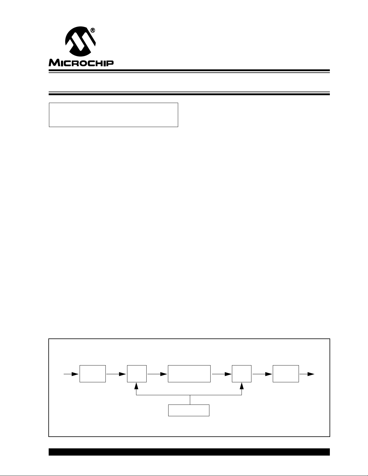
A typical signal processing system includes an A/D
converter, D/A converter, and CPU that performs the
signal processing algorithm as shown in Figure 1.
The input signal,
filter (commonly called the anti-aliasing filter) whose
function is to bandlimit the signal to below the Nyquist
rate (one half the sampling frequency) to prevent
aliasing. The signal is then digitized by the A/D
converter at a rate determined by the sample clock to
produce
system transfer function,
in the time-domain using a difference equation. The
output sample,
continuous-time signal,
output low-pass filter.
The calculation of the output signal using a difference
equation requires a multiply and accumulate (MAC)
operation. This is typically a single-cycle instruction on
DSP chips but can take many cycles to perform on a
standard microcontroller since it must be implemented
in code. Since the digitization of the signal, calculation
of the output, and output to the D/A converter all must
be completed within the sample clock period, the speed
at which this can be done determines the maximum
bandwidth that can be achieved with the system. The
relatively slow speed of most microcontrollers is the
major limitation when they are used in DSP applications but the PIC16C74’s fast instruction execution
speed (as fast as 200 ns/instruction) can provide the
performance required to implement relatively low bandwidth systems. In addition, the device’ s on-chip A/D and
PWM modules provide all the functions needed for a
single chip system. Only a few external components
are needed to use the PIC16C74 for tone generation,
filtering of transducer signals, or low bandwidth control.
x(n)
x(t)
, is first passed through an input
, the discrete-time input sequence. The
H(z)
, is typically implemented
y(n)
, is then converted back into the
y(t)
, by the D/A converter and
FIGURE 1: TYPICAL SIGNAL PROCESSING SYSTEM
X[t]
1997 Microchip Technology Inc. DS00616A-page 1
Low-pass
Filter
A/D
X[n]
H[z]
System Clock
Y[n]
D/A
Low-pass
Filter
Y[t]
Page 2

AN616
CODE DEVELOPMENT TOOLS
The code for these applications was written using
Byte Craft’s MPC C compiler . The MPC compiler provides
an Integrated Development Environment (IDE) and generates highly optimized code for the entire PICmicro™
family. For new PICmicro users that are familiar with C,
this is an ideal way to quickly develop code for these
processors. In addition, the listing files can be studied in
order to learn the details of PICmicro assembly language.
The modules and examples for this application note use
C for the main program body and in-line assembly language for the time-critical routines. MPC provides interrupt support so that interrupt service routines (ISRs) can
be easily written in either C or assembly. This f eature was
used to provide a timer ISR for one of the code modules.
The compiler proved to be a valuable tool that allowed
both high level and assemb ly language routines to be written and tested quickly.
In order to provide the double precision math functions
required for this application note, a couple of existing
math functions written for the PIC16C54 (AN525,
gramming PIC16C5X Devices on Logical Devices
converted for use with MPC. The double precision multiply
and addition routines were modified by first changing all
RAM declarations done in EQU statements to C
“
unsigned char
assembly language code was preceded by “ #asm ” and
ended by “ #endasm ” preprocessor directives which tell
the compiler where the in-line assembly code starts and
ends. Finally , an y macro sections and register names that
are defined differently in MPC were changed.
The assembly language routines for tone generation and
filtering were also written as C functions using the compiler. Assembly language routines written in this way can
be called directly from other assembly language modules
or called directly from C by using the label name as a C
function. Source listings for all the modules and example
programs can be found in the appendices at the end of
this application note. These modules can be directly compiled using the MPC compiler or, alternatively, the assembly language sections can be used with MPASM with
minor modifications.
” variable declarations. The main body of
Number Representation and Math Routines
One of the challenges of using any general purpose
microcontroller for signal processing algorithms is in
implementing the finite word-length arithmetic required to
perform the calculations. As mentioned before, the speed
at which the MAC operations can be performed limits the
maximum achievab le bandwidth of the system. Theref ore,
the routines that perform the multiplication and the main
signal processing algorithms need to be optimized for
speed in order to obtain the highest possible bandwidth
when using the PIC16C74.
The selection of word size and coefficient scaling are also
important factors in the successful implementation of signal processing systems. The effects of using a fixed word
length to represent the signal and do calculations fall into
Pro-
) were
three categories: signal quantization, round-off error, and
coefficient quantization. The signal quantization due to
the A/D converter and round-off error due to the finite precision arithmetic affect the overall signal-to-noise
performance of the system. Scaling of the input signal
should be done before the A/D converter to use the full
input range and maximize the input signal-to-noise ratio.
The use of double precision math for all calculations and
storing intermediate results, even if the input and output
signals are represented as 8-bit words, will help to reduce
the round-off error noise to acceptable levels. Coefficient
quantization occurs when the calculated coefficients are
truncated or rounded off to fit within the given word length.
This has the effect of moving the system transf er function
poles and zeros which can change the system gain, critical frequencies of filters, or stability of the system. The
successful implementation of these systems requires
careful design and modeling of these effects using one of
the many software programs that are available. The code
written for this application note was first modeled using
PC MA TLAB bef ore being implemented on the PIC16C74.
The algorithms in this application note are all
implemented using fixed point two’s compliment
arithmetic. Two math libraries were used for the
examples: one 8-bit signed multiply routine that was written specifically for the tone generation algorithm, and the
modified double precision routines for the PIC16C54 that
were used in the filtering routine. All numbers are stored
in fractional two’s compliment for mat where the MSB is
the sign bit and there is an implied decimal point right after
it. This is commonly referred to as Qx format where the
number after the Q represents the number of fractional
bits in the word. For instance, 16 bit words with the decimal point after the MSB would be referred to as Q15. This
format allows numbers over the range of -1 to 0.99 to be
represented and, because the magnitude of all numbers
is less than or equal to one, has the advantage that there
can be no overflow from a multiplication operation.
Since calculations are done using two’s compliment arithmetic, values read by the PIC16C74’ s A/D con verter need
to be converted to this format. This can be easily done if
the input is set up to read values in offset binary format.
In this representation, the most negative input voltage is
assigned to the number 0, zero volts is assigned the number 128, and the most positive voltage input is assigned
255. Since the PIC16C74 has a unipolar input A/D converter, a bipolar input signal must be scaled to be between
0 and 5V. One way to accomplish this is to use an op-amp
scaling and offset circuit. The signal should be centered
at 2.5V and have a peak to peak voltage swing of
4 to 4.5V. The offset binar y number can be converted to
two’s compliment format by simply complimenting the
MSB of the word. Once the signal processing calculations
are completed, the number can be converted back to offset binary by complimenting the MSB before it is written
to the PWM module. A similar level shifting circuit can be
used at the PWM output to restore the DC level of the signal. Using this technique allows a wide range of analog
input voltages to be handled by the PIC16C74.
DS00616A-page 2
1997 Microchip Technology Inc.
Page 3

AN616
A/D and D/A Conversion
The PIC16C74’s internal 8-bit A/D converter and PWM
modules can be used to implement analog I/O for the system. The A/D converter along with an external anti-aliasing filter provides the analog input for the system.
Depending on the input signal bandwidth and the sampling frequency, the filter can be a simple single pole RC
filter or a multiple pole active filter . The PWM output along
with an external output “smoothing” filter provides the D/A
output for the system. This can be a simple RC filter if the
PWM frequency is much higher (five to ten times) than the
analog signal that is being output. Alternatively, an active
filter can also be used at the PWM output . Since the use
of the A/D and PWM modules is covered in detail in the
data sheet for the part, they will not be covered here. In
addition, since the PIC16C74’s A/D conv erter is similar to
the PIC16C71 and the PWM module is the same as the
PIC16C74, the use of these is also covered in application
notes AN546, AN538, and AN539.
Appendix A contains the listing for the C module “
GIO.C
” that has the functions that read the A/D conv erter
input, initialize the PWM module, and write 8-bit values to
the PWM module. The number format (offset binary or
two’s compliment) f or the A/D and PWM v alues as well as
the PWM resolution and mode are set using “ #define ”
pragmas at the beginning of the module. The
get_sample() function takes the A/D input multiplexor
channel number as an argument and returns the measured input value. The init_PWM() function takes the
PWM period register PR2 value as an argument. The
write_PWM() function takes the output values for PWM
module1 and 2 and writes them to the appropriate registers using the specified resolution. If the second argument
to the function is 0, the registers for PWM module 2 are
unaffected. The PWM resolution is always 8-bits but the
mode used depends on the PWM frequency.
The A/D conversions need to be perf ormed at the system
sample rate which requires that some form of sample
clock be generated internally or input from an external
source. One way to generate this clock internally, in software with minimal effort, is to use the Timer2 interrupt.
Since Timer2 is used to generate the PWM period,
enabling the Timer2 interrupt and using the Timer2
postscaler can generate an interrupt at periods that are
integer divisors of the PWM period. The ISR can set a
software “sample flag” that is checked by the main routine .
Once the sample flag is asserted by the ISR, the main
routine can then clear it and perform the signal processing
operation, output the next sample, and then wait for the
sample flag to be asserted true again. Alternatively, a
separate timer/counter or external clock input can be
used for the system sample clock. The latter two methods
have the advantage that the PWM frequency can be set
independent of the sampling period. For best results, the
PWM frequency should be set for at least five times the
maximum frequency of the analog signal that is bring
reproduced. The example programs illustrate the use of
both of the methods for generating an internal sample
clock.
ANALO-
Tone Generation
For systems that need to provide audible feedback or to
provide DTMF signaling for telcom applications, the
PIC16C74’s PWM module can be used to generate these
signals. One wa y to do this is to output samples of a sin usoidal waveform to the PWM module at the system sampling rate. This method is relatively simple but is limited to
single tones and may require large amounts of memory
depending on the number of samples used per cycle of
the wavefor m and the number of tones that need to be
generated. A more efficient method of generating both
single and dual-tone signals is to use a difference equation method. This method uses a difference equation that
is derived from the z-transform of a sinusoid as follows:
The z-transform of a sinusoid is
1–
z
ω
--------------------------------------------------1 2z
where the period ω = 2 πƒ and T is the sampling period.
If this is interpreted as the transfer function
H(z) = Y(z)/X(z) then the difference equation can be found
taking the inverse z-transform and applying the associated shift theorem as follows:
rearranging:
-1
Y(z)(1 - 2z
Y(z) = z
taking the inverse z-transform:
-1
Z
[Y(z)] = Z-1[z-1X(z)sinωT + z-1Y(z)2cosωT - z-2Y(z)]
y(n) = sin
If we let
written as:
y(n) = a x(n - 1) + 2b y(n - 1) - y(n - 2)
thus we have a diff erence equation with coefficients
b
. Note that only two coefficients are needed to generate
a sinusoidal output sequence. These are calculated from
the relationship above and stored in memory for use by
the tone generation algorithm.
If we input an impulse to this system (x(n) = 1 at n = 0 and
is zero elsewhere) then the output of the system will be a
discrete-time sinusoidal sequence. Note that at n = 0, the
output will always be 0 and x(n) is only 1 at n = 1 so the
sequence becomes:
cosωT + z-2) = X(z)(z-1sinωT)
-1
X(z)sinωT + z-1Y(z)2cosωT - z-2Y(z)
ω
T x(n - 1) + 2cosωT y(n - 1) - y(n - 2)
a = sin ω T
and
y(0) = 0
y(1) = a
y(n) = 2b y(n - 1) - y(n - 2)
for n equal to or greater than 2
Tsin
1–
ω
Tcos– z2–+
b = cos ω T
, the equation can be
a
and
1997 Microchip Technology Inc. DS00616A-page 3
Page 4
AN616
In order to further simplify the implementation of the algorithm, we can omit the first sample period. Since the output is already at 0 before starting, this will make no
difference in the final output other than the fact that it will
be time shifted by one sample. To generate dual tones,
the algorithm is executed once for each tone and the two
output samples are summed together. Since the output
must be calculated and output to the D/A each sample
period, a limitation exists on the frequency of the tone that
can be produced for a given sample rate and processor
speed. The higher the ratio of the sample clock to the tone
frequency , the better , b ut a sample rate of at least three to
four times the highest tone output should produce a sine
wave with acceptable distortion.
Appendix B contains the listing for the “ PICTONE.C ” module which uses the difference equation method to produce
variable length tones from the PWM module. Timer2 is
used to generate the PWM period as well as the sample
clock and tone duration timer. To send a tone, the coefficients and duration are written to the appropriate variables and then the tone routine is called. If the a2 and b2
coefficients are cleared, the routine will only generate a
single tone sequence. The difference equation algorithm
uses 8-bit signed math routines for the multiply operations. Using 8-bit coefficients reduces the accuracy by
which the tones can be generated but greatly reduces the
number of processor cycles needed to perform the algorithm since only single precision arithmetic is used. The
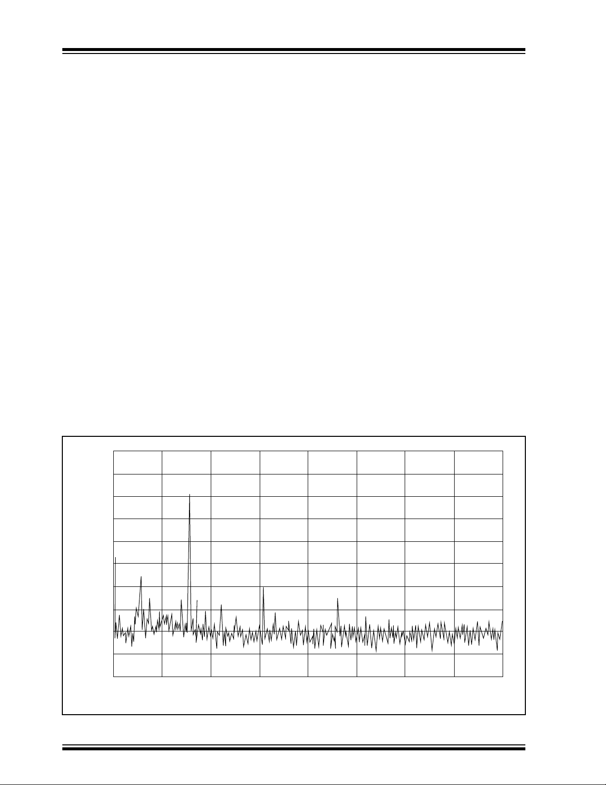
spectrum of a single tone signal generated using this routine is shown in Figure 2.
Note that the second harmonic is better than 40 dB below
the fundamental. Accuracy of this particular tone is better
than 0.5%.
An example program “ DTMFGEN.C ” illustrates the use of
the tone module to generate the 16 standard DTMF tones
used for dialing on the telephone system. A sampling rate
of 6.5 kHz was used which allows dual tones to be generated on a processor running at 10 MHz. Accuracy with
respect to the standard DTMF frequencies is better than
1% for all tones and all harmonics above the fundamental
frequency are greater than 30 dB down.
FIGURE 2: SINGLE TONE SIGNAL
0.0
-10
-20
-30
-40
-50
-60
-70
Relative Amplitude (dB)
-80
-90
-100
0.0 500 1.0k 1.5k 2.0k 2.5k 3.0k 3.5k
PIC16C74 Tone Generation Routine Output Spectrum - 770 Hz Fundamental
Frequency (Hz)
DS00616A-page 4
1997 Microchip Technology Inc.
Page 5
AN616
Digital Filters
Digital filters with critical frequencies up to a kilohertz or
so can be implemented on the PIC16C74. Digital filters
fall into two classes: Finite Impulse Response (FIR) and
Infinite Impulse Response (IIR) filters. FIR filters require
more coefficients and multiplication operations to implement practical filters and are not as well suited for implementation on the PIC16C74. IIR type filters are typically
designed starting with an analog filter prototype and then
performing an analog to digital transformation to produce
the digital filter coefficients. The subject of digital filter
design is not within the scope of this application note but
there are many excellent texts that cover the theory and
design of these filters.
The implementation of a second-order IIR filter is done by
using a second-order difference equation. A
second-order infinite impulse response (IIR) filter has a
transfer function of the form:
b
+ b1z-1 + b2z
H(z) =
Where a
polynomials of the system transfer function that, when
factored, yield the system poles and zeros. The difference
equation found by taking the inverse z-transform and
applying the shift theorem is:
y(n) =
b
Since the transfer function coefficients are used directly in
the difference equation, this is often called the “Direct
Form I” implementation of a digital filter. This form has its
limitations due to numerical accuracy issues but is effective for implementing second-order systems.
Appendix C contains the listing for the general-purpose
filter routine “ IIR_FILT.C ” that can be used to implement low-pass, high-pass, bandpass, and bandstop
(notch) filters. The filter() function takes an 8-bit input
value x(n) and calculates the output value y(n) . The filter
coefficients are stored as 16-bit two’s compliment
numbers and computation of the output is done using
double precision arithmetic. Since the coefficients
generated from the filter design program will be in decimal
form, they need to be scaled to be less than 1 and then
multiplied by 32,768 to put them in Q15 format. Additional
scaling by factors of two may be required to prevent overflow of the sum during calculations. If this is done, the output must be multiplied by this scale factor to account for
this. The “ IIR_FILT.C ” module contains two other subroutines required for the filtering program. One if these is
a decimal adjust subroutine to restore the decimal place
after two 16-bit Q15 numbers are multiplied. The subroutine shifts the 32-bit result left by one to get rid of the extra
, a
, b
1
x(n) + b1x(n - 1) + b2x(n - 2) - a1y(n - 1) - a2y(n - 2)
0
, b
2
0
0
1 + a1z-1 + a2z
, and b
1
are the coefficients of the
2
-2
-2
sign bit. The other routine scales the output by factors of
two and is used after the output of the filter has been
calculated to account for the scaling of the coefficients.
An example program “ NOTCH_60.C ” is provided that illustrates the implementation of a 60 Hz notch filter using the
“ IIR_FILT.C ” module. The filter was modeled and
designed using PC MATLAB before being implemented
on the PIC16C74. A sample rate of 1 kHz is used which
means that signals up to a few hundred hertz can be processed. The filter provides an attenuation of about 40 dB
at 60 Hz and can be used to remove interference from
sensor signals in a system.
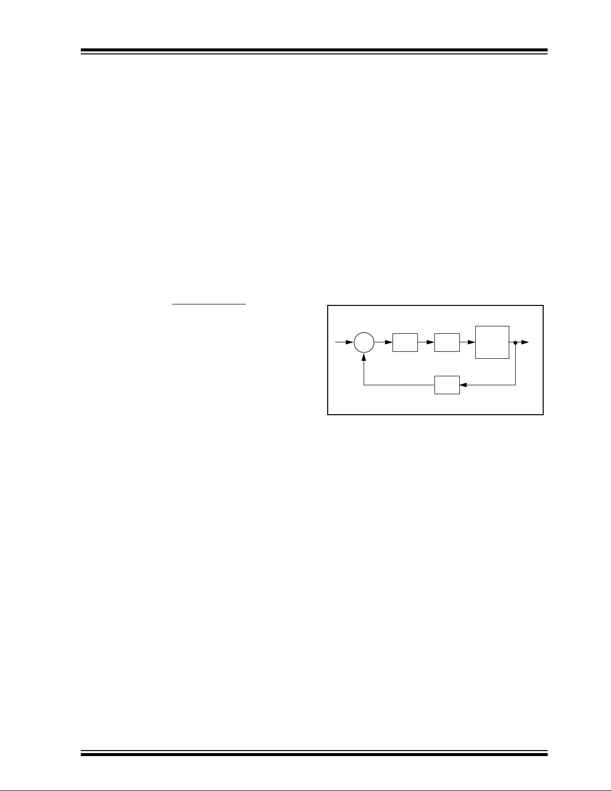
Digital Control
A low bandwidth digital control system can be
implemented on the PIC16C74 using the analog I/O and
IIR filter routines. A typical digital control system is shown
below:
FIGURE 3: TYPICAL DIGITAL CONTROL
SYSTEM
r
+
The input, r , is the reference input and
continuous-time output of the system.
transfer function of the plant (controlled system) and
is the digital compensator. The error signal is calculated
by subtracting the measured output signal,
reference. The controller transfer function is essentially a
filter that is implemented in the time-domain using a difference equation. Since digital control system design is a
complex subject and the design of a suitable compensator depends on the system being controlled and the performance specifications, only the implementation issues
will be discussed.
e[n]
∑
K[z]
-
D/A
y[n]
A/D
G[s]
Plant
y(t)
G(s)
is the analog
y[t]
is the
K(z)
y(n)
, from the
1997 Microchip Technology Inc. DS00616A-page 5
Page 6
AN616
One popular and well understood compensator is the Proportional-Integral-Derivative (PID) controller whose transfer function is of the form:
K
K(z) = KP +
Where
K
is the proportional gain,
,and
implemented directly or can be put in the form of a standard second-order difference equation from the modified
transfer function as shown below:
Since the numerator coefficients will be greater than one,
a gain factor
ing coefficients are less than one. In this way, the IIR filter
routine can be used to implement the controller. After the
filter routine, the output
before being output to the PWM module. Since the gain
can be high, this result needs to be checked for overflow
and limited to the maximum 8-bit value, if required. Saturating the final result prevents the system from going
unstable if overflo w in the math does occur . The gains can
also be applied externally at the D/A output. F or e xample ,
the PWM can drive a power op-amp driver that provides a
± 20 volt swing for a DC motor.
P
K
is the derivative gain. The transfer function can be
D
H(z) =
y(n) =
(KIT2 + KPT + KD) - (2KD + KPT)z-1 + KDz
(K
+ KIT +
P
2K
- (KP +
K
+
T
D
T
D
x(n - 2) - y(n - 1)
K
needs to be factored out so that the result-
I
+ KD(1 - z-1)
-1
1 - z
K
is the integral gain
I
T(1 - z-1)
K
D
)x(n)
T
)x(n - 1)
y
needs to be multiplied by
-2
RESULTS AND CONCLUSION
The results obtained using the PIC16C74 in these applications were impressive. The tone generation routines
produce very clean sinusoidal signals and DTMF tones
generated using this routine have been used to dial numbers over the telephone system with excellent results. In
addition, tones used for audible f eedback are more pleasing to the ear than those generated from a port pin as is
typically done on processors without PWM modules.
Using the PIC16C74 to generate these tones eliminates
the need for special DTMF generator IC’s thus reducing
the cost and simplifying the design. The tone routine
requires approximately 125 instruction cycles to calculate
an output sample for a single tone output and
230 instruction cycles to calculate an output sample for a
dual tone output.
The IIR filtering routines produce good results and have
been used to filter 60 Hz signals on sensor lines and also
to implement a simple PID controller system with excellent
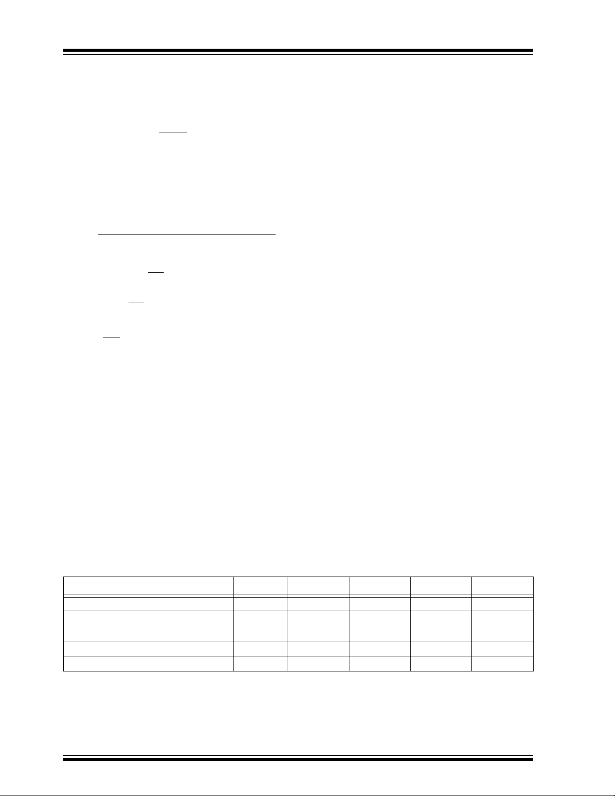
results. The IIR routine takes approximately 1670 instruction cycles to calculate the output. Table 1 shows the performance that can be expected with the PIC16C74 for
various processor speeds.
In conclusion, the PIC16C74 provides the necessary performance to provide these simple, low bandwidth signal
processing operations. This means that products using
this device can benefit from cost and power savings by
eliminating specialized components that normally perform these tasks.
K
References
Antoniou, A. Digital Filters: Analysis and Design. NY:
McGraw-Hill Book Co., 1979.
Openheim, A.V. and Schafer, R.W. Digital Signal
Processing. Englewood Cliffs, N.J.: Prentice-Hall, Inc.,
1975.
TABLE 1: PIC16C74 IIR FILTER PERFORMANCE
4 MHz 8 MHz 10 MHz 16 MHz 20 MHz
A/D Input (35 cycles + 15 µs) 50 µs 32.5 29 23.75 22
IIR Filter (1850 cycles) 1850 925 740 462.5 370
PWM Output (62 cycles) 62 31 24.8 15.5 12.4
Total 1962 988.5 793.8 501.75 368.4
Max. Sampling Frequency ~500 Hz ~1000 Hz ~1250 Hz ~2000 Hz ~2500 Hz
DS00616A-page 6
1997 Microchip Technology Inc.
Page 7
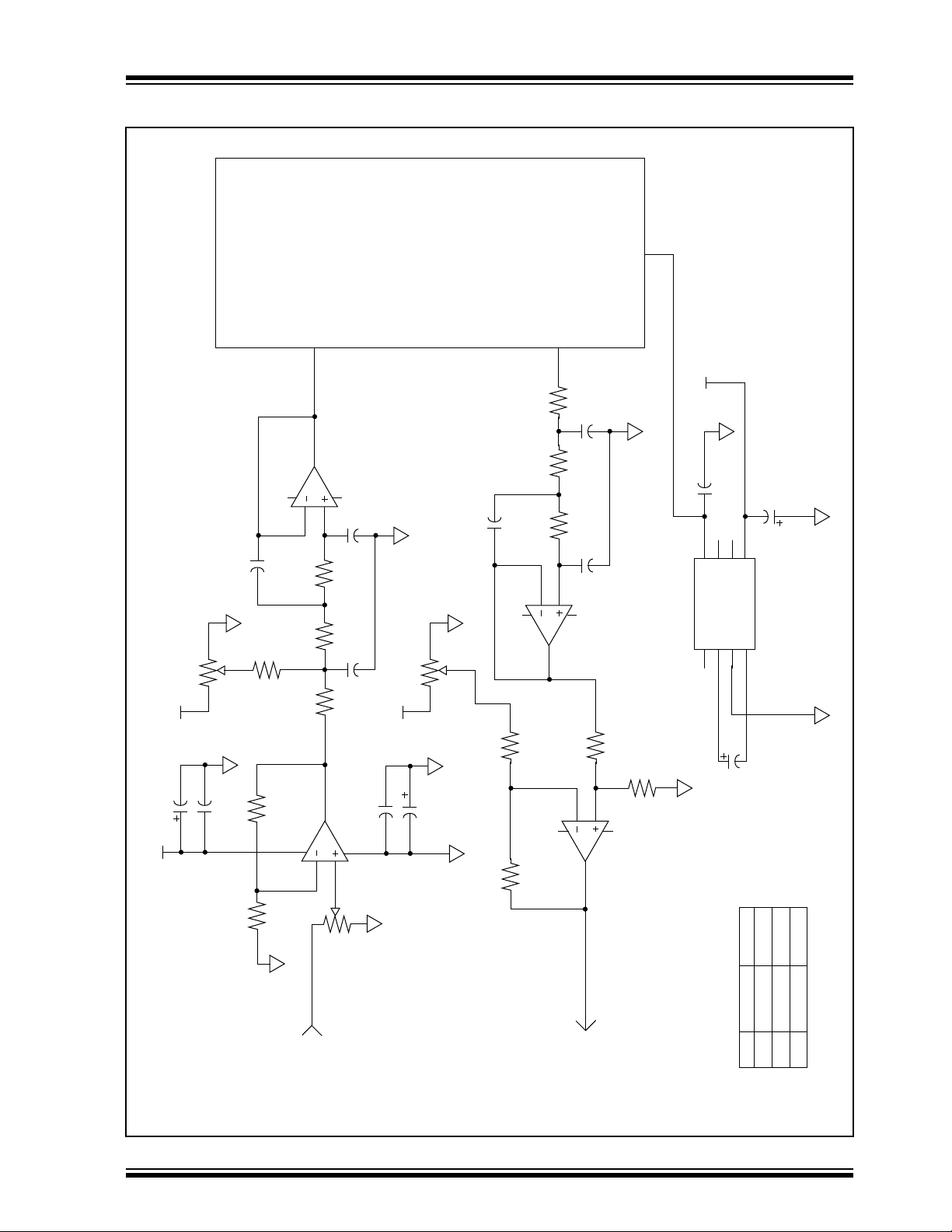
FIGURE 4: SCHEMATIC
Board
PICDEM2
(See Figure 5)
AN616
+V (12 VDC In)
100k
Input Offset Adjust
VR1
+5V
10 µF
C9
C12
+V (12 VDC In)
RA1
7
U1B
LM324
5
6
(see table)
Ca
20k
R10
0.1 µF
100k
R11
11
10k
R4
Cc
(see table)
10k 10k
Cb
(see table)
R2 R1
10k
Output Offset Adjust
C13
VR3
+5V
10 µF
C10
10k
1 R3
U1A
0.1 µF
LM324
3
VR2
4
47k
2
(see table)
Ca
470k
R13
470k
R12
RC1
-V
Cb
(see table)
0.1 µF
C11
10k 10k 10k
U2
876
V+
OSCLVVD
C+
NC
123
Cc
(see table)
R6 R5 R7
9
10
8
U1C
LM324
10k
R9
12
13
14
U1D
10k
R8
LM324
5
GND
4
10 µF
C8
10 µF
C7
C-
LMC7660IN
250 Hz 3.4 kHz
Ca 1 µF 0.082 µF
Cb 0.15 µF 0.012 µF
Cc 0.0039 µF 300 pF
Signal In
(DC Coupled)
Input Level Adjust
Signal Output
(DC Coupled)
Capacitor Values for 250 Hz and 3.4 kHz
3 Pole Chebyshev Filter - 1 dB Passband Ripple
1997 Microchip Technology Inc. DS00616A-page 7
Page 8
AN616
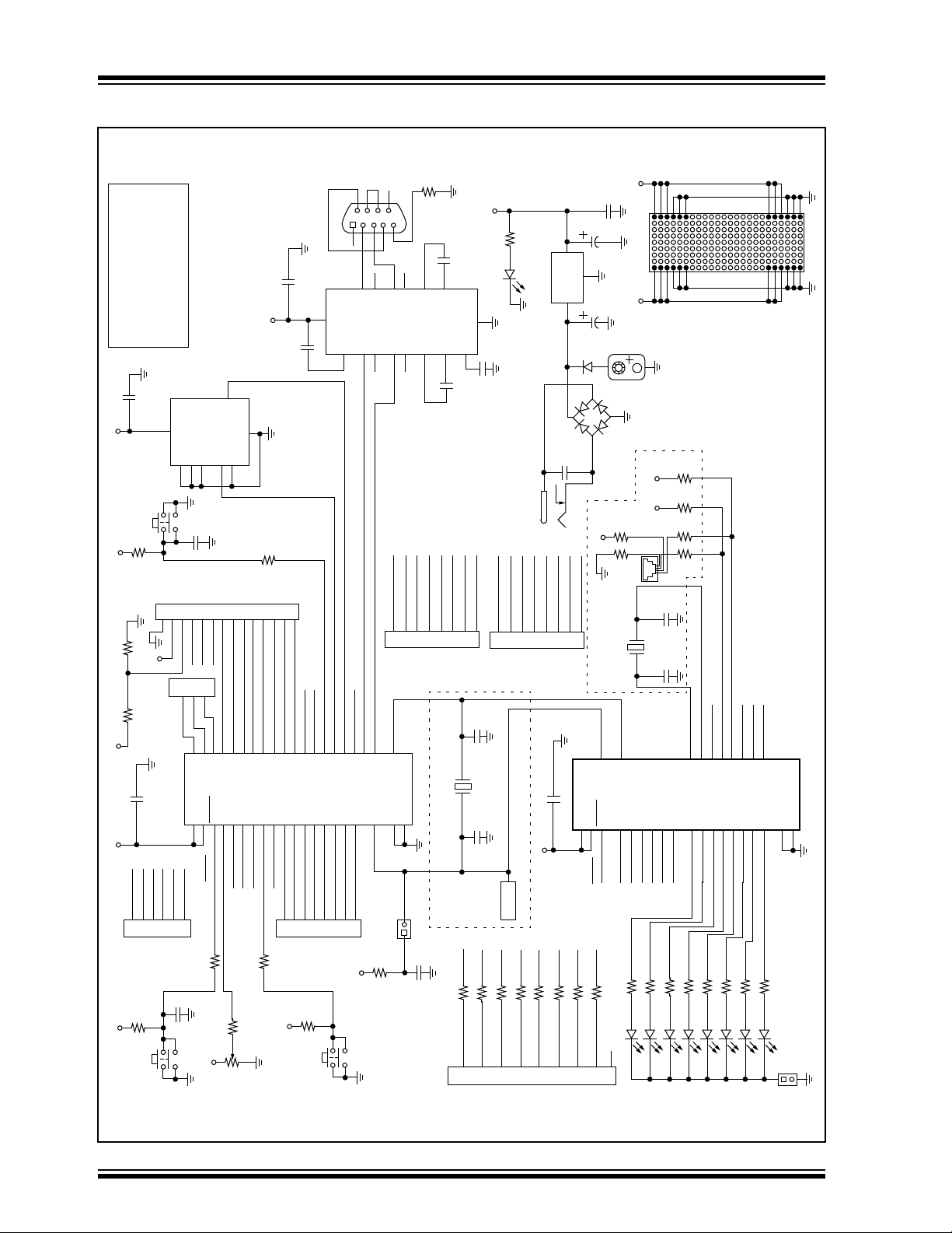
FIGURE 5: PICDEM2 SCHEMATIC TIE-IN
Notes:
C10
+5V
+5V
R6
R5
C2
+5V +5V
RA
+5V
Unless otherwise specified,
resistance values are in ohms,
5% 1/4W. Capacitance values
0.1
S3
R7
4.7k
1
330
+5V
10k
0.1
RA0
RA12RA23RA34RA45RA5
1
R1
4.7k
S1
8
RE
U4
are in microfarads.
2
1
C1
VDD
A0
3J34
RE0
U1
6
0.1
24LC01B
A1
A2
2
3
0.1
C9
RA15RA26RA3
RE1
RE2
9
10
8
RE0
RE1
VDD
VDD
11
32
MCLR 12RA0
470
R17
+5V
5
SDA
SCL
6
7
For
LCD
19 RD0 7
RE2
RD0
RA0
MCLR
R2
R16
WP
DSPLY
20 RD1 8
RD1
RA1
RA13RA2 4
SS
V
RD2 922RD3
21
RD2
RA2
R18
470
5k
10
RD3
RA3 5
11
RD4
27
RA3
RA46RA5 7
470
+5V
R19
RD4
RA4
470
28 RD51229 RD6 13
RD5
RA5
RB
C11
RD6
RB0 331
+5V
0.1
0.1
C12
30 RD71415 OSO
RD7
RB0
RB1
RB1 342
RB2 353
16 OSI
RC0
RB2
RB3 364
R3
RC1
RB3
4.7k
S2
U3
16
17 RC2
RC2
RB4
RB4 375
VCC
18 SCL
RB5 386RB6 397
J1
2
23 SDA
RC3
RB5
678
12345
7
14
T1OUT
MAX232A
V+
T1IN
10
11
TX
24 RC5
25 TX
26 RX
RC4
RC5
RC6
RB6
RB7
131231
RB7 40
8
+5V
9
13
T2OUT
T2IN
12
RX
1 (RC0) OSO
RC
OSC2
14
RC7
OSC1
R4
4.7k
8
R1IN
R2IN
R1OUT
R2OUT
9
2 (RC1) OSI
3 RC2
OSC2
Vss
Vss
OSC1
J7
10
R14
C15
4
C2+
C1+
1
C13
4 (RC3) SCL
5 (RC4) SDA
PIC16C64
Provision Only
C3
20 pF
J4
Keyboard
+5V+5V
0.1
C19
+5V
RB7
X1
PIC16C73
Vss
Vss
8
19
J6
470
R15
0.1
D1
GRN
15
0.1
1 RD0
RD
RN3
2 RD1
Not Populated
Y2
OUT
RB2
RN3
3
3
3 RD2
TXCO
RB3
4
4
Power
4 RD3
RN3
J2
RB4
3
5
LM78L05
1
3
5 RD4
6 RD5
C8
+5V
RB5
RN3
4
6
5
C2-
GND
V-
C1-
6
3
0.1
C14
6 RC5
7 (RC6) TX
8 (RC7) RX
C5
Y1
TBD
20 pF 20 pF
C4
RB1
RB0
RN3
RN3
4
1
2
C18
OUT
U5
COM
IN
220
C17
CR2
1N914
4
1
2
CR1
0.01
C16
2
DJ005A
+5V
7 RD6
8 RD7
Provision Only
OSC1
9
U2
0.1
MCLR
VDD
1
20
MCLR
RB7
RB6
RN3
RN3
4
4
789
9 Pin Header
220
J8
W02M
3
R9
R8
Not Populated
OSC2
10
OSC1
RA0 2
+9V
Battery
10
10
Y3
OSC2
RA0
RA1
RA1 3
RB0
RN1
D2
Breadboard
+5V +5V
J5
C7
TBD
C6
RA2
RA3
RA4
RA2 4
RA3 5
RA4 6
RB2
RB1
RN1
RN1
D4
D3
R13
R12
R11
R10
20 pF
20 pF
OSO12OSI13RC214SCL15SDA
11
RA5
RA5 7
RB021RB122RB223RB324RB4 25
RB3
RN1
D5
820
820
10
10
RC0
RB0
RC1
RB1
RB4
RN2
D6
RC2
RB2
RN2
RC3
RB3
RB5
D7
RC517TX18RX
16
RC4
RC5
RB4
RB5
RB5 26
RB6 27
RB6
RN2
D8
RC6
RB6
RN2
RC7
28
RB7
RB7
D9
DS00616A-page 8 1997 Microchip Technology Inc.
Page 9

AN616
Please check the Microchip BBS for the latest version of the source code. Microchip’s Worldwide Web Address:
www.microchip.com; Bulletin Board Support: MCHIPBBS using CompuServe
®
(CompuServe membership not
required).
APPENDIX A:ANALOG I/O MODULE
/****************************************************************************
* Analog I/O Module
*
* Written for “Digital Signal Processing with the PIC16C74” Application Note
*
* This module contains functions that read the A-D inputs, initialize the PWM
* ports, and write values to the PWM ports.
*
* D. Mostowfi 4/95
****************************************************************************/
#define active 1 /* define active as 1 */
#define LOW 0 /* define LOW as 0 */
#define HIGH 1 /* define HIGH as 1 */
#define OFFSET 0 /* define offset binary mode as 0 */
#define TWOS 1 /* define two’s compliment mode as 1 */
#define AD_FORMAT TWOS /* define A-D format as TWOS */
#define PWM_FORMAT TWOS /* define PWM format as TWOS */
#define PWM_RES HIGH /* define PWM resolution as HIGH */
bits FLAGS; /* general purpose flags */
#define sample_flag FLAGS.1 /* define sample_flag as FLAGS.1 */
/*****************************************************************************
* A-D Converter Routine - reads A-D converter inputs
*
* usage:
* - call get_sample(channel #)
* - returns 8 bit value
*****************************************************************************/
char get_sample(char channel)
{
char i;
ADRES=0; /* clear ADRES */
STATUS.C=0; /* clear carry */
RLCF(channel); /* and rotate channel 3 times */
RLCF(channel); /* to put in proper position */
RLCF(channel); /* for write to ADCON0 */
ADCON0=channel; /* write channel to ADCON0 */
ADCON0.0=1; /* turn on A-D */
i=0; /* set delay loop variable to 0 */
while(i++<=5){}; /* delay (to ensure min sampling time) */
ADCON0.2=1; /* start conversion */
while(ADCON0.2){} /* wait for eoc */
ADCON0.0=0; /* turn off a-d converter */
if(AD_FORMAT==TWOS){ /* if format is two’s compliment */
ADRES.7=!ADRES.7; /* compliment MSB */
}
return ADRES; /* return value in a-d result reg */
}
/******************************************************************************
* PWM Initialization Routine - sets up PR2, sets output to mid-point, and
* starts timer 2 with interrupts disabled.
*
* usage:
1997 Microchip Technology Inc. DS00616A-page 9
Page 10

AN616
* - call init_PWM(PR2 register value)
******************************************************************************/
void init_PWM(char _pr2)
{
PR2=_pr2; /* reload value for 40khz PWM period */
CCP1CON.5=0; /* set CCPxCON = 0 for 50% output */
CCP1CON.4=0;
CCP2CON.5=0;
CCP2CON.4=0;
if(PWM_RES==HIGH){ /* if resolution is high, set CCPRxH=0 and */
CCPR1H=0x00; /* CCPRxL=0x20 for 50% PWM duty cycle */
CCPR1L=0x20;
CCPR2H=0x00;
CCPR2L=0x20;
}
else{
CCPR1H=0x00; /* if resolution is low, set CCPRxH=0 and */
CCPR1L=0x80; /* CCPRxL=0x80 for 50% PWM duty cycle */
CCPR2H=0x00;
CCPR2L=0x80;
}
T2CON.TMR2ON=1; /* start timer 2 */
PIE1.TMR2IE=0; /* and disable timer 2 interrupt */
}
/*******************************************************************************
* PWM Output Routine - writes output values to PWM ports
*
* Both high resolution and low resolution modes write 8 bit values - use of
* high or low resolution depends on PWM output period.
*
* usage:
* - call write_PWM(channel 1 value, channel 2 value)
* if channel 2 value=0, PWM port 2 not written
*******************************************************************************/
void write_PWM(bits pwm_out1, bits pwm_out2)
{
if(PWM_FORMAT==TWOS){ /* if format is two’s compliment */
pwm_out1.7=!pwm_out1.7; /* compliment msb’s */
pwm_out2.7=!pwm_out1.7;
}
if(PWM_RES==HIGH){ /* if resolution is high */
STATUS.C=0; /* clear carry */
pwm_out1=RRCF(pwm_out1); /* rotate right and write two lsb’s */
CCP1CON.4=STATUS.C; /* to CCP1CON4 and CCP1CON5 */
STATUS.C=0;
pwm_out1=RRCF(pwm_out1);
CCP1CON.5=STATUS.C;
if(pwm_out2!=0){ /* if pwm_out2 not 0, do the same */
STATUS.C=0; /* for channel 2 */
pwm_out2=RRCF(pwm_out2);
CCP2CON.4=STATUS.C;
STATUS.C=0;
pwm_out2=RRCF(pwm_out2);
CCP2CON.5=STATUS.C;
}
}
CCPR1L=pwm_out1; /* write value to CCPR1L */
if(pwm_out2!=0){ /* if pwm_out2 not 0, do the same */
CCPR2L=pwm_out2; /* for CCPR2L */
}
} /* done */
DS00616A-page 10 1997 Microchip Technology Inc.
Page 11

AN616
Please check the Microchip BBS for the latest version of the source code. Microchip’s Worldwide Web Address:
www.microchip.com; Bulletin Board Support: MCHIPBBS using CompuServe
®
(CompuServe membership not
required).
APPENDIX B:TONE GENERATION MODULE
/*****************************************************************************
* Tone Generation Module
*
* Written for “Digital Signal Processing with the PIC16C74” Application Note.
*
* This module contains a C callable module that generates single or dual
* tones using a difference equation method:
*
* y1(n)=a1*x(n-1)+b1*y1(n-1)-y1(n-2)
* y2(n)=a2*x(n-1)+b2*y2(n-1)-y2(n-2)
*
* The routine is written in assembly language and uses the optimized signed
* 8x8 multiply routine and scaling routine in the file 8BITMATH.C.
*
* D. Mostowfi 2/95
*****************************************************************************/
#include “\mpc\apnotes\8bitmath.c” /* 8 bit signed math routines */
#define sample_flag FLAGS.1 /* sample flag */
#define no_tone2 FLAGS,2 /* no tone 2 flag */
extern char ms_cntr; /* millisecond counter for tone loop */
char a1; /* first tone (low-group) coeeficient 1 */
char a2; /* first tone (low-group) coefficient 2 */
char b1; /* second tone (high group) coefficient 1 */
char b2; /* second tone (high group) coefficient 2 */
char duration; /* tone duration */
char y1; /* output sample y1(n) for tone 1 */
char y2; /* output sample y2(n) for tone 2 */
/******************************************************************************
* Tone function - generates single or dual tone signals out PWM port 1.
*
* usage:
* - write coefficients for tone 1 to a1 and b1
* - write coefficents for tone 2 to a2 and b2 (0 if no tone 2)
* - write duration of tone in milliseconds to duration
* - call tone() function
*******************************************************************************/
void tone(void)
{
char y1_1; /* y1(n-1) */
char y1_2; /* y1(n-2) */
char y2_1; /* y2(n-1) */
char y2_2; /* y2(n-2) */
PIR1.TMR2IF=0; /* clear timer 2 interrupt flag */
PIE1.TMR2IE=1; /* and enable timer 2 interrupt */
ms_cntr=0; /* clear ms counter */
STATUS.RP0=0; /* set proper bank!!! */
#asm
clrf y1 ; clear output byte and taps
clrf y2 ;
clrf y1_1 ;
clrf y1_2 ;
1997 Microchip Technology Inc. DS00616A-page 11
Page 12

AN616
clrf y2_1 ;
clrf y2_2 ;
bcf no_tone2 ; clear no tone 2 flag
clrf ms_cntr ; clear millisecond counter
first_sample:
movf a1,W ; first iteration
movwf y1 ; y1(n)=a1
movwf y1_1 ;
movlw 0x00 ;
iorwf a2,W ;
btfsc STATUS,Z ; generate second tone (a2 !=0) ?
bsf no_tone2 ;
movf a2,W ; y2(n)=a2
movwf y2 ;
movwf y2_1 ;
movf y2,W ;
addwf y1,F ; y1(n)=y1(n)+y2(n) (sum two tone outputs)
tone_loop:
movf ms_cntr,W ; test to see if ms=duration (done?)
subwf duration,W ;
btfsc STATUS,Z ;
goto tone_done ;
wait_PWM:
btfss FLAGS,1 ; test sample flag (sample period elapsed?)
goto wait_PWM ; loop if not
bcf FLAGS,1 ; if set, clear sample flag
#endasm
write_PWM((char)y1,0); /* write y1 to PWM port */
#asm
next_sample:
movf b1,W ; y1(n)=b1*y1(n-1)-y1(n-2)
movwf multcnd ;
movf y1_1,W ;
movwf multplr ;
call _8x8smul ;
call scale_16 ;
movf y1_2,W ;
subwf result_l,W ;
movwf y1 ;
movf y1_1,W ; y1(n-2)=y1(n-1)
movwf y1_2 ;
movf y1,W ; y1(n-1)=y1(n)
movwf y1_1 ;
btfsc no_tone2 ;
goto tone_loop ;
movf b2,W ; y2(n)=b2*y2(n-1)-y2(n-2)
movwf multcnd ;
movf y2_1,W ;
movwf multplr ;
call _8x8smul ;
call scale_16 ;
movf y2_2,W ;
subwf result_l,W ;
movwf y2 ;
movf y2_1,W ; y2(n-2)=y2(n-1)
movwf y2_2 ;
movf y2,W ; y2(n-1)=y2(n)
movwf y2_1 ;
DS00616A-page 12 1997 Microchip Technology Inc.
Page 13

movf y2,W ;
addwf y1,F ; y1(n)=y1(n)+y2(n) (sum two tone outputs)
goto tone_loop ; go and calculate next sample
tone_done:
#endasm
CCP1CON.5=0; /* reset PWM outputs to mid value */
CCP1CON.4=0;
CCP2CON.5=0;
CCP2CON.4=0;
CCPR1H=0x00;
CCPR1L=0x20;
CCPR2H=0x00;
CCPR2L=0x20;
PIE1.TMR2IE=0; /* disable timer 2 interrupts */
PIR1.TMR2IF=0; /* and clear timer 2 interrupt flag */
}
AN616
1997 Microchip Technology Inc. DS00616A-page 13
Page 14

AN616
Please check the Microchip BBS for the latest version of the source code. Microchip’s Worldwide Web Address:
www.microchip.com; Bulletin Board Support: MCHIPBBS using CompuServe
®
(CompuServe membership not
required).
APPENDIX C:DTMF TONE GENERATION
/*****************************************************************************
* DTMF tone generation using PIC16C74
*
* Written for the “Digital Signal Processing Using the PIC16C74” Ap Note
*
* Generates 16 DTMF tones (1-9,0,*,#,A,B,C,D) out PWM port 1
*
* Uses PICTONE.C and ANALOGIO.C modules
*
* D. Mostowfi 4/95
******************************************************************************/
#include “\mpc\include\delay14.h”
#include “\mpc\include\16c74.h” /* c74 header file */
#include “\mpc\math.h”
#include “\mpc\apnotes\analogio.c” /* analog I/O module */
#include “\mpc\apnotes\pictone.c” /* tone generation module */
bits pwm1;
/* Function Prototypes */
void main_isr();
void timer2_isr();
/* 16C74 I/O port bit declarations */
/* global program variables */
char tmr2_cntr; /* timer 2 interrupt counter */
char delay_cntr; /* delay time counter (10ms ticks)*/
/* Tone Coefficients for DTMF Tones */
const DTMF_1[4]={30, 51, 48, 27};
const DTMF_2[4]={30, 51, 56, 19};
const DTMF_3[4]={30, 51, 64, 11};
const DTMF_4[4]={33, 48, 48, 27};
const DTMF_5[4]={33, 48, 56, 19};
const DTMF_6[4]={33, 48, 64, 11};
const DTMF_7[4]={36, 45, 48, 27};
const DTMF_8[4]={36, 45, 56, 19};
const DTMF_9[4]={36, 45, 64, 11};
const DTMF_0[4]={40, 41, 56, 19};
const DTMF_star[4]={40, 41, 48, 27};
const DTMF_pound[4]={40, 41, 64, 11};
const DTMF_A[4]={30, 51, 75, 2};
const DTMF_B[4]={33, 48, 75, 2};
const DTMF_C[4]={36, 45, 75, 2};
const DTMF_D[4]={40, 41, 75, 2};
/*****************************************************************************
* main isr - 16C74 vectors to 0004h (MPC __INT() function) on any interrupt *
* assembly language routine saves W and Status registers then tests flags in
* INTCON to determine source of interrupt. Routine then calls appropriate isr.
* Restores W and status registers when done.
DS00616A-page 14 1997 Microchip Technology Inc.
Page 15

*****************************************************************************/
void __INT(void)
{
if(PIR1.TMR2IF){ /* timer 2 interrupt ? */
PIR1.TMR2IF=0; /* clear interrupt flag */
timer2_isr(); /* and call timer 2 isr */
}
/* Restore W, WImage, and STATUS registers */
#asm
BCF STATUS,RP0 ;Bank 0
MOVF temp_PCLATH, W
MOVWF PCLATH ;PCLATH restored
MOVF temp_WImage, W
MOVWF __WImage ;__WImage restored
MOVF temp_FSR, W
MOVWF FSR ;FSR restored
SWAPF temp_STATUS,W
MOVWF STATUS ;STATUS restored
SWAPF temp_WREG,F
SWAPF temp_WREG,W ;W restored
#endasm
}
AN616
/****************************************************************************
* timer 2 isr - provides PWM sample clock generation and millisecond counter
* for tone routine
*****************************************************************************/
void timer2_isr(void)
{
sample_flag=active; /* set sample flag (150us clock) */
PORTB.7=!PORTB.7; /* toggle PORTB.7 at sample rate */
if(tmr2_cntr++==7){ /* check counter */
tmr2_cntr=0; /* reset if max */
ms_cntr++; /* and increment millisecond ticks */
}
}
void main()
{
/* initialize OPTION register */
OPTION=0b11001111;
/* initialize INTCON register (keep GIE inactive!) */
INTCON=0b00000000; /* disable all interrupts */
/* initialize PIE1 and PIE2 registers (peripheral interrupts) */
PIE1=0b00000000; /* disable all interrupts */
PIE2=0b00000000;
/* initialize T1CON and T2CON registers */
T1CON=0b00000000; /* T1 not used */
T2CON=0b00101000; /* T2 postscaler=5 */
/* initialize CCPxCON registers */
CCP1CON=0b00001100; /* set CCP1CON for PWM mode */
CCP2CON=0b00001100; /* set CCP2CON for PWM mode (not used in demo) */
/* initialize SSPCON register */
SSPCON=0b00000000; /* serial port - not used */
1997 Microchip Technology Inc. DS00616A-page 15
Page 16

AN616
/* initialize ADCONx registers */
ADCON0=0b00000000; /* A-D converter */
ADCON1=0b00000010;
/* initialize TRISx register (port pins as inputs or outputs) */
TRISA=0b00001111;
TRISB=0b00000000;
TRISC=0b10000000;
TRISD=0b00001111;
TRISE=0b00000000;
/* clear watchdog timer (not used) */
CLRWDT();
/* initialize program variables */
tmr2_cntr=0;
/* initialize program bit variables */
FLAGS=0b00000000;
/* intialize output port pins (display LED’s on demo board) */
PORTB=0;
/* enable interrupts... */
INTCON.ADIE=1; /* Peripheral interrupt enable */
INTCON.GIE=1; /* global interrupt enable */
init_PWM(0x3e); /* initialize PWM port */
PORTB=0x01; /* write a 1 to PORTB */
a1=DTMF_1[0]; /* and send a DTMF “1” */
b1=DTMF_1[1];
a2=DTMF_1[2];
b2=DTMF_1[3];
duration=150;
tone();
Delay_Ms_20MHz(200); /* delay 100ms (200/2 using MPC delays) */
PORTB=0x02; /* write a 2 to PORT B */
a1=DTMF_2[0]; /* and send a DTMF “2” */
b1=DTMF_2[1];
a2=DTMF_2[2];
b2=DTMF_2[3];
duration=150;
tone();
Delay_Ms_20MHz(200); /* delay 100ms (200/2 using MPC delays) */
PORTB=0x03; /* write a 3 to PORTB */
a1=DTMF_3[0]; /* and send a DTMF “3” */
b1=DTMF_3[1];
a2=DTMF_3[2];
b2=DTMF_3[3];
duration=150;
tone();
Delay_Ms_20MHz(200); /* delay 100ms (200/2 using MPC delays) */
PORTB=0x04; /* write a 4 to PORTB */
a1=DTMF_4[0]; /* and send a DTMF “4” */
b1=DTMF_4[1];
DS00616A-page 16 1997 Microchip Technology Inc.
Page 17

a2=DTMF_4[2];
b2=DTMF_4[3];
duration=150;
tone();
Delay_Ms_20MHz(200); /* delay 100ms (200/2 using MPC delays) */
PORTB=0x05; /* write a 5 to PORTB */
a1=DTMF_5[0]; /* and send a DTMF “5” */
b1=DTMF_5[1];
a2=DTMF_5[2];
b2=DTMF_5[3];
duration=150;
tone();
Delay_Ms_20MHz(200); /* delay 100ms (200/2 using MPC delays) */
PORTB=0x06; /* write a 6 to PORTB */
a1=DTMF_6[0]; /* and send a DTMF “6” */
b1=DTMF_6[1];
a2=DTMF_6[2];
b2=DTMF_6[3];
duration=150;
tone();
Delay_Ms_20MHz(200); /* delay 100ms (200/2 using MPC delays) */
PORTB=0x07; /* write a 7 to PORTB */
a1=DTMF_7[0]; /* and send a DTMF “7” */
b1=DTMF_7[1];
a2=DTMF_7[2];
b2=DTMF_7[3];
duration=150;
tone();
Delay_Ms_20MHz(200); /* delay 100ms (200/2 using MPC delays) */
AN616
PORTB=0x08; /* write a 8 to PORTB */
a1=DTMF_8[0]; /* and send a DTMF “8” */
b1=DTMF_8[1];
a2=DTMF_8[2];
b2=DTMF_8[3];
duration=150;
tone();
Delay_Ms_20MHz(200); /* delay 100ms (200/2 using MPC delays) */
PORTB=0x09; /* write a 9 to PORTB */
a1=DTMF_9[0]; /* and send a DTMF “9” */
b1=DTMF_9[1];
a2=DTMF_9[2];
b2=DTMF_9[3];
duration=150;
tone();
Delay_Ms_20MHz(200); /* delay 100ms (200/2 using MPC delays) */
PORTB=0x0; /* write a 0 to PORTB */
a1=DTMF_0[0]; /* and send a DTMF “0” */
b1=DTMF_0[1];
a2=DTMF_0[2];
b2=DTMF_0[3];
duration=150;
tone();
Delay_Ms_20MHz(200); /* delay 100ms (200/2 using MPC delays) */
Delay_Ms_20MHz(200); /* delay 100ms (200/2 using MPC delays) */
1997 Microchip Technology Inc. DS00616A-page 17
Page 18

AN616
PORTB=0x0e; /* write a 0x0e to PORTB */
a1=DTMF_star[0]; /* and send a DTMF “*” */
b1=DTMF_star[1];
a2=DTMF_star[2];
b2=DTMF_star[3];
duration=250;
tone();
Delay_Ms_20MHz(200); /* delay 100ms (200/2 using MPC delays) */
PORTB=0x0f; /* write a 0x0f to PORTB */
a1=DTMF_pound[0]; /* and send a DTMF “#” */
b1=DTMF_pound[1];
a2=DTMF_pound[2];
b2=DTMF_pound[3];
duration=250;
tone();
Delay_Ms_20MHz(200); /* delay 100ms (200/2 using MPC delays) */
Delay_Ms_20MHz(200); /* delay 100ms (200/2 using MPC delays) */
PORTB=0x0a; /* write a 0x0a to PORTB */
a1=DTMF_A[0]; /* and send a DTMF “A” */
b1=DTMF_A[1];
a2=DTMF_A[2];
b2=DTMF_A[3];
duration=250;
tone();
Delay_Ms_20MHz(200); /* delay 100ms (200/2 using MPC delays) */
PORTB=0x0b; /* write a 0x0b to PORTB */
a1=DTMF_B[0]; /* and send a DTMF “B” */
b1=DTMF_B[1];
a2=DTMF_B[2];
b2=DTMF_B[3];
duration=250;
tone();
Delay_Ms_20MHz(200); /* delay 100ms (200/2 using MPC delays) */
PORTB=0x0c; /* write a 0x0c to PORTB */
a1=DTMF_C[0]; /* and send a DTMF “C” */
b1=DTMF_C[1];
a2=DTMF_C[2];
b2=DTMF_C[3];
duration=250;
tone();
Delay_Ms_20MHz(200); /* delay 100ms (200/2 using MPC delays) */
PORTB=0x0d; /* write a 0x0d to PORTB */
a1=DTMF_D[0]; /* and send a DTMF “D” */
b1=DTMF_D[1];
a2=DTMF_D[2];
b2=DTMF_D[3];
duration=250;
tone();
PORTB=0; /* write a 0 to PORTB */
while(1){} /* done (loop) */
}
DS00616A-page 18 1997 Microchip Technology Inc.
Page 19

AN616
Please check the Microchip BBS for the latest version of the source code. Microchip’s Worldwide Web Address:
www.microchip.com; Bulletin Board Support: MCHIPBBS using CompuServe
®
(CompuServe membership not
required).
APPENDIX D:IIR FILTER MODULE
/*****************************************************************************
* Second-Order IIR Filter Module
*
* Written for “Digital Signal Processing with the PIC16C74” Application Note.
*
* This routine implements an IIR filter using a second order difference
* equation of the form:
*
* y(n) = b0*x(n)+b1*x(n-1)+b2*x(n-2)+a1*y(n-1)+a2*y(n-2)
*
* D. Mostowfi 3/95
*****************************************************************************/
#include “\mpc\apnotes\dbl_math.c”
bits x_n; /* input sample x(n) */
unsigned long y_n; /* output sample y(n) */
unsigned long x_n_1; /* x(n-1) */
unsigned long x_n_2; /* x(n-2) */
unsigned long y_n_1; /* y(n-1) */
unsigned long y_n_2; /* y(n-2) */
char rmndr_h; /* high byte of remainder from multiplies */
char rmndr_l; /* low byte of remainder from multiplies */
#define A1_H 0xd2 /* filter coefficients */
#define A1_L 0x08 /* for 60Hz notch filter */
#define A2_H 0x11 /* Fs= 1kHz */
#define A2_L 0x71
#define B0_H 0x18
#define B0_L 0xbb
#define B1_H 0xd2
#define B1_L 0x08
#define B2_H 0x18
#define B2_L 0xb9
/******************************************************************************
* Filter initialization - clears all taps in memory.
*
* usage:
* - call init_filter()
* use at program initialization
******************************************************************************/
void init_filter(){
#asm
clrf y_n ; clear output value
clrf y_n+1 ;
clrf y_n_1 ; and all filter “taps”
clrf y_n_1+1 ;
clrf y_n_2 ;
clrf y_n_2+1 ;
clrf x_n_1 ;
clrf x_n_1+1 ;
clrf x_n_2 ;
clrf x_n_2+1 ;
#endasm
1997 Microchip Technology Inc. DS00616A-page 19
Page 20

AN616
}
/******************************************************************************
* Assembly language subroutines for main filter() function
******************************************************************************/
#asm
;
; Add Remainder subroutine - adds remainder from multiplies to ACCc
;
add_rmndr:
btfss sign,7 ; check if number is negative
goto add_r_start ; go to add_r_start if not
comf ACCcLO ; if so, negate number in ACC
incf ACCcLO ;
btfsc STATUS,Z ;
decf ACCcHI ;
comf ACCcHI ;
btfsc STATUS,Z ;
comf ACCbLO ;
incf ACCbLO ;
btfsc STATUS,Z ;
decf ACCbHI ;
comf ACCbHI ;
add_r_start:
movf rmndr_l,W ; get low byte of remainder
addwf ACCcLO ; and add to ACCcLO
btfsc STATUS,C ; check for overflow
incf ACCcHI ; if overflow, increment ACCcHI
movf rmndr_h,W ; get high byte of remainder
addwf ACCcHI ; and add to ACCcHI
btfsc STATUS,C ; check for overflow
incf ACCbLO ; if overflow, increment ACCbLO
btfss sign,7 ; check if result negative
goto add_r_done ; if not, go to add_r_done
comf ACCcLO ; if so, negate result
incf ACCcLO ;
btfsc STATUS,Z ;
decf ACCcHI ;
comf ACCcHI ;
btfsc STATUS,Z ;
comf ACCbLO ;
incf ACCbLO ;
btfsc STATUS,Z ;
decf ACCbHI ;
comf ACCbHI ;
add_r_done:
retlw 0 ; done
;
; Decimal Adjust Subroutine - used after each Q15 multiply to convert Q30 result
; to Q15 number
dec_adjust:
bcf sign,7 ; clear sign
btfss ACCbHI,7 ; test if number is negative
goto adjust ; go to adjust if not
bsf sign,7 ; set sign if negative
comf ACCcLO ; and negate number
incf ACCcLO
DS00616A-page 20 1997 Microchip Technology Inc.
Page 21

btfsc STATUS,Z
decf ACCcHI
comf ACCcHI
btfsc STATUS,Z
comf ACCbLO
incf ACCbLO
btfsc STATUS,Z
decf ACCbHI
comf ACCbHI
adjust:
rlf ACCcHI ; rotate ACC left 1 bit
rlf ACCbLO ;
rlf ACCbHI ;
btfss sign,7 ; check if result should be negative
goto adj_done ; if not, done
comf ACCbLO ; if result negative, negate ACC
incf ACCbLO
btfsc STATUS,Z
decf ACCbHI
comf ACCbHI
adj_done:
retlw 0 ; done
AN616
;
; Output Scaling Routine - used to scale output samples by factors of
; 2, 4, or 8 at end of filter routine
;
scale_y_n:
bcf sign,7 ; clear sign,7
btfss y_n+1,7 ; test if y(n) negative
goto start_scale ; go to start_scale if not
bsf sign,7 ; set sign,7 if negative
comf y_n ; and compliment y(n)
incf y_n ;
btfsc STATUS,Z ;
decf y_n+1 ;
comf y_n+1 ;
start_scale:
bcf STATUS,C ; clear carry
rlf y_n+1 ; and rotate y(n) left
rlf y_n ;
bcf STATUS,C ;
rlf y_n+1 ;
rlf y_n ;
bcf STATUS,C ;
rlf y_n+1 ;
rlf y_n ;
btfss sign,7 ; test if result is negative
goto scale_y_done ; go to scale_y_done if not
comf y_n ; negate y(n) if result is negative
incf y_n ;
btfsc STATUS,Z ;
decf y_n+1 ;
comf y_n+1 ;
scale_y_done:
retlw 0 ; done
#endasm
1997 Microchip Technology Inc. DS00616A-page 21
Page 22

AN616
/******************************************************************************
* Filter function - filter takes current input sample, x(n), and outputs next
* output sample, y(n).
*
* usage:
* - write sample to be filtered to x_n
* - call filter()
* - output is in MSB of y_n (y_n=MSB, y_n+1=LSB)
*
******************************************************************************/
void filter(){
#asm
clrf y_n ; clear y(n) before starting
clrf y_n+1 ;
clrf ACCbLO ; move x(n) to ACCbHI
movf x_n,W ; (scale 8 bit - 16 bit input)
movwf ACCbHI ;
movlw B0_H ; get coefficient b0
movwf ACCaHI ; y(n)=b0*x(n)
movlw B0_L ;
movwf ACCaLO ;
call D_mpyF ;
movf ACCcHI,W ; save remainder from multiply
movwf rmndr_h ;
movf ACCcLO,W ;
movwf rmndr_l ;
call dec_adjust ;
movf ACCbHI,W ;
movwf y_n+1 ;
movf ACCbLO,W ;
movwf y_n ;
movlw B1_H ; get coefficient b1
movwf ACCaHI ; y(n)=y(n)+b1*x(n-1)
movlw B1_L ;
movwf ACCaLO ;
movf x_n_1+1,W ;
movwf ACCbHI ;
movf x_n_1,W ;
movwf ACCbLO ;
call D_mpyF ;
call add_rmndr ; add in remainder from previous multiply
movf ACCcHI,W ; and save new remainder
movwf rmndr_h ;
movf ACCcLO,W ;
movwf rmndr_l ;
call dec_adjust ;
movf y_n+1,W ;
movwf ACCaHI ;
movf y_n,W ;
movwf ACCaLO ;
call D_add ;
movf ACCbHI,W ;
movwf y_n+1 ;
movf ACCbLO,W ;
movwf y_n ;
movlw B2_H ; get coefficient b2
movwf ACCaHI ; y(n)=y(n)+b2*x(n-2)
movlw B2_L ;
movwf ACCaLO ;
movf x_n_2+1,W ;
DS00616A-page 22 1997 Microchip Technology Inc.
Page 23

movwf ACCbHI ;
movf x_n_2,W ;
movwf ACCbLO ;
call D_mpyF ;
call add_rmndr ; add in remainder from previous multiply
movf ACCcHI,W ; and save new remainder
movwf rmndr_h ;
movf ACCcLO,W ;
movwf rmndr_l ;
call dec_adjust ;
movf y_n+1,W ;
movwf ACCaHI ;
movf y_n,W ;
movwf ACCaLO ;
call D_add ;
movf ACCbHI,W ;
movwf y_n+1 ;
movf ACCbLO,W ;
movwf y_n ;
movlw A1_H ; get coefficient a1
movwf ACCaHI ; y(n)=y(n)+a1*y(n-1)
movlw A1_L ;
movwf ACCaLO ;
movf y_n_1+1,W ;
movwf ACCbHI ;
movf y_n_1,W ;
movwf ACCbLO ;
call D_mpyF ;
call add_rmndr ; add in remainder from previous multiply
movf ACCcHI,W ; and save new remainder
movwf rmndr_h ;
movf ACCcLO,W ;
movwf rmndr_l ;
call dec_adjust ;
movf y_n+1,W ;
movwf ACCaHI ;
movf y_n,W ;
movwf ACCaLO ;
call D_sub ;
movf ACCbHI,W ;
movwf y_n+1 ;
movf ACCbLO,W ;
movwf y_n ;
AN616
movlw A2_H ; get coefficient a2
movwf ACCaHI ; y(n)=y(n)+a2*y(n-2)
movlw A2_L ;
movwf ACCaLO ;
movf y_n_2+1,W ;
movwf ACCbHI ;
movf y_n_2,W ;
movwf ACCbLO ;
call D_mpyF ;
call add_rmndr ;
call dec_adjust ;
movf y_n+1,W ;
movwf ACCaHI ;
movf y_n,W ;
movwf ACCaLO ;
call D_sub ;
movf ACCbHI,W ;
movwf y_n+1 ;
movf ACCbLO,W ;
movwf y_n ;
1997 Microchip Technology Inc. DS00616A-page 23
Page 24

AN616
movf x_n_1,W ; x(n-2)=x(n-1)
movwf x_n_2 ;
movf x_n_1+1,W ;
movwf x_n_2+1 ;
movf x_n,W ; x(n-1)=x(n)
movwf x_n_1+1 ;
clrf x_n_1 ;
movf y_n_1,W ; y(n-2)=y(n-1)
movwf y_n_2 ;
movf y_n_1+1,W ;
movwf y_n_2+1 ;
movf y_n,W ; y(n-1)=y(n)
movwf y_n_1 ;
movf y_n+1,W ;
movwf y_n_1+1 ;
call scale_y_n ;
movf y_n+1,W ; shift lsb of y_n to msb
movwf y_n ;
#endasm
}
DS00616A-page 24 1997 Microchip Technology Inc.
Page 25

AN616
Please check the Microchip BBS for the latest version of the source code. Microchip’s Worldwide Web Address:
www.microchip.com; Bulletin Board Support: MCHIPBBS using CompuServe
®
(CompuServe membership not
required).
APPENDIX E: NOTCH FILTER
/*****************************************************************************
* 60 Hertz Notch Filter
*
* Written for “Digital Signal Processing with the PIC16C74” Application Note.
*
* This example program use the filter() function to implement a 60Hz notch
* filter. T0 is used to generate a 1kHz sample clock. The program samples the
* input signal x(n) on A-D channel 1, calls the filter routine signal, and
* outputs y(n) to PWM channel 1.
*
* If FILTER set to 0, performs straight talkthru from A-D to PWM output.
* T0 period can be changed to cary the sample rate.
*
* D. Mostowfi 4/95
******************************************************************************/
#include “\mpc\include\16c74.h” /* c74 header file */
#include “\mpc\apnotes\analogio.c” /* analog I/O module */
#include “\mpc\apnotes\iir_filt.c” /* iir filter module */
#define FILTER 1
/* Function Prototypes */
void main_isr();
void timer0_isr();
/*****************************************************************************
* main isr - 16C74 vectors to 0004h (MPC __INT() function) on any interrupt *
* assembly language routine saves W and Status registers then tests flags in
* INTCON to determine source of interrupt. Routine then calls appropriate isr.
* Restores W and status registers when done.
*****************************************************************************/
void __INT(void)
{
if(INTCON.T0IF){ /* timer 0 interrupt ? */
INTCON.T0IF=0; /* clear interrupt flag */
timer0_isr(); /* and call timer 0 isr */
}
/* Restore W, WImage, and STATUS registers */
#asm
BCF STATUS,RP0 ;Bank 0
MOVF temp_PCLATH, W
MOVWF PCLATH ;PCLATH restored
MOVF temp_WImage, W
MOVWF __WImage ;WImage restored
MOVF temp_FSR, W
MOVWF FSR ;FSR restored
SWAPF temp_STATUS,W
MOVWF STATUS ;RP0 restored
SWAPF temp_WREG,F
SWAPF temp_WREG,W ;W restored
#endasm
}
/*****************************************************************************
* timer 0 interrupt service routine
***************************************************************************/
void timer0_isr(void)
1997 Microchip Technology Inc. DS00616A-page 25
Page 26

AN616
{
TMR0=100; /* reload value for 1ms period */
PORTB.0=!PORTB.0; /* toggle PORTB.0 */
sample_flag=active; /* set sample flag */
}
void main()
{
/* initialize OPTION register */
OPTION=0b00000011; /* assign prescaler to T0 */
/* initialize INTCON register (keep GIE inactive!) */
INTCON=0b00000000; /* disable all interrupts */
/* initialize PIE1 and PIE2 registers (periphreal interrupts) */
PIE1=0b00000000; /* disable all peripheral interrupts */
PIE2=0b00000000;
/* initialize T1CON and T2CON registers */
T1CON=0b00000000; /* T1 not used */
T2CON=0b00000000; /* T2 not used */
/* initialize CCPxCON registers */
CCP1CON=0b00001100; /* set CCP1CON for PWM mode */
CCP2CON=0b00000000; /* CCP2CON=0 (PWM 2 not used) */
/* initialize SSPCON register */
SSPCON=0b00000000; /* serial port - not used */
/* initialize ADCONx registers */
ADCON0=0b00000000; /* a-d converter */
ADCON1=0b00000010;
/* initialize TRISx register (port pins as inputs or outputs) */
TRISA=0b00001111;
TRISB=0b00000000;
TRISC=0b11111011;
TRISD=0b11111111;
TRISE=0b11111111;
/* clear watchdog timer (not used) */
CLRWDT();
/* initialize program bit variables */
FLAGS=0b00000000;
/* intialize output port pins */
PORTB=0;
/* enable interrupts... */
INTCON.T0IE=1; /* peripheral interrupt enable */
INTCON.GIE=1; /* global interrupt enable */
init_PWM(0x40); /* init PWM port */
init_filter(); /* init filter */
while(1){
while(!sample_flag){} /* wait for sample clock flag to be set */
sample_flag=0; /* clear sample clock flag */
x_n=get_sample(1); /* read ADC channel 1 into x(n) */
if(FILTER==1){ /* if filter enabled */
filter(); /* call filter routine */
}
else{ /* or else write x(n) to y(n) (talkthru) */
y_n=x_n;
}
write_PWM((char)y_n,0); /* write y_n to PWM port 1 */
}
DS00616A-page 26 1997 Microchip Technology Inc.
Page 27

AN616
Please check the Microchip BBS for the latest version of the source code. Microchip’s Worldwide Web Address:
www.microchip.com; Bulletin Board Support: MCHIPBBS using CompuServe
®
(CompuServe membership not
required).
APPENDIX F: 8-BIT MULTIPLY AND SCALING ROUTINES
/******************************************************************************
* 8 bit Multiply and Scaling Routines
*
* Written for “Digital Signal Processing with the PIC16C74” Application Note.
*
*
* This module provides a 8 bit signed multiply and scaling routine for the
* PICTONE.C tone generation program. The routines are adapted from “Math
* Routines for the 16C5x” in Microchip’s Embedded Controller Handbook.
*
* All numbers are assumed to be signed 2’s compliment format.
*
* D. Mostowfi 11/94
*******************************************************************************/
char multcnd; /* 8 bit multiplicand */
char multplr; /* 8 bit multiplier */
char result_h; /* result - high byte */
char result_l; /* result - low byte */
char sign; /* result sign */
#asm
;
; 8x8 signed multiply routine
; called from PICTONE.C module (assembly language routine)
;
.MACRO mult_core bit
btfss multplr,bit
goto \no_add
movf multcnd,W
addwf result_h,F
\no_add:
rrf result_h
rrf result_l
.ENDM
_8x8smul:
movf multcnd,W ; get multiplicand
xorwf multplr,W ; and xor with multiplier
movwf sign ; and save sign of result
btfss multcnd,7 ; check sign bit of multiplicand
goto chk_multplr ; go and check multipier if positive
comf multcnd ; negate if negative
incf multcnd ;
chk_multplr:
btfss multplr,7 ; check sign bit of multiplier
goto multiply ; go to multiply if positive
comf multplr ; negate if negative
incf multplr ;
multiply:
movf multcnd,W ; set up multiply registers
bcf STATUS,C ;
clrf result_h ;
clrf result_l ;
mult_core 0 ; and do multiply core 8 times
mult_core 1 ;
1997 Microchip Technology Inc. DS00616A-page 27
Page 28

AN616
mult_core 2 ;
mult_core 3 ;
mult_core 4 ;
mult_core 5 ;
mult_core 6 ;
mult_core 7 ;
set_sign:
btfss sign,7 ; test sign to see if result negative
retlw 0 ; done if not! (clear W)
comf result_l ; negate result if sign set
incf result_l ;
btfsc STATUS,Z ;
decf result_h ;
comf result_h ;
retlw 0 ; done (clear W)
;
; Scaling Routine (used after a multiply to scale 16 bit result)
; Operates on result_h and result_l - final result is in result_l
; routine divides by 32 to restore Q7 result of 2*b*y(n-1) in tone
; generation algorithm
;
scale_16:
btfss sign,7 ; test if negative (sign set from mult)
goto start_shift ; go to start shift if pos.
comf result_l ; negate first if neg.
incf result_l ;
btfsc STATUS,Z ;
decf result_h ;
comf result_h ;
start_shift:
bcf STATUS,C ; clear status
rrf result_h ; and shift result left 5x (/32)
rrf result_l ;
rrf result_h ;
rrf result_l ;
rrf result_h ;
rrf result_l ;
rrf result_h ;
rrf result_l ;
rrf result_h ;
rrf result_l ;
btfss sign,7 ; test if result negative
goto scale_done ; done if not negative
comf result_l ; negate result if negative
incf result_l ;
btfsc STATUS,Z ;
decf result_h ;
comf result_h ;
scale_done: ;
retlw 0 ; done (clear W)
#endasm
DS00616A-page 28 1997 Microchip Technology Inc.
Page 29

AN616
Please check the Microchip BBS for the latest version of the source code. Microchip’s Worldwide Web Address:
www.microchip.com; Bulletin Board Support: MCHIPBBS using CompuServe
®
(CompuServe membership not
required).
APPENDIX G:DOUBLE PRECISION MATH ROUTINES
/******************************************************************************
* Double Precision Math Routines
*
* This module contains assembly language routines from “Math Routines for the
* 16C5x” from Microchip’s Embedded Controller Handbook that have been adapted
* for use with the Bytecraft MPC C Compiler.
*
* Routines are used IIR_FILT.C module written for “Digital Signal Processing
* with the PIC16C74” Application Note.
*
* D. Mostowfi 3/95
*****************************************************************************/
/*
Start of converted MPASM modules:
;*******************************************************************
; Double Precision Addition & Subtraction
;
;*******************************************************************;
; Addition : ACCb(16 bits) + ACCa(16 bits) -> ACCb(16 bits)
; (a) Load the 1st operand in location ACCaLO & ACCaHI ( 16 bits )
; (b) Load the 2nd operand in location ACCbLO & ACCbHI ( 16 bits )
; (c) CALL D_add
; (d) The result is in location ACCbLO & ACCbHI ( 16 bits )
;
; Performance :
; Program Memory : 07
; Clock Cycles : 08
;*******************************************************************;
; Subtraction : ACCb(16 bits) - ACCa(16 bits) -> ACCb(16 bits)
; (a) Load the 1st operand in location ACCaLO & ACCaHI ( 16 bits )
; (b) Load the 2nd operand in location ACCbLO & ACCbHI ( 16 bits )
; (c) CALL D_sub
; (d) The result is in location ACCbLO & ACCbHI ( 16 bits )
;
; Performance :
; Program Memory : 14
; Clock Cycles : 17
;*******************************************************************;
;
*/
char ACCaLO; //equ 10 changed equ statements to C char variables
char ACCaHI; //equ 11
char ACCbLO; //equ 12
char ACCbHI; //equ 13
;
#asm /* start of in-line assembly code */
; include “mpreg.h” commented out these
; org 0 two lines (MPASM specific)
;*******************************************************************
; Double Precision Subtraction ( ACCb - ACCa -> ACCb )
;
D_sub call neg_A2 ; At first negate ACCa; Then add
;
;*******************************************************************
1997 Microchip Technology Inc. DS00616A-page 29
Page 30

AN616
; Double Precision Addition ( ACCb + ACCa -> ACCb )
;
D_add movf ACCaLO,W
addwf ACCbLO ;add lsb
btfsc STATUS,C ;add in carry
incf ACCbHI
movf ACCaHI,C
addwf ACCbHI ;add msb
retlw 0
neg_A2 comf ACCaLO ; negate ACCa ( -ACCa -> ACCa )
incf ACCaLO
btfsc STATUS,Z
decf ACCaHI
comf ACCaHI
retlw 0
;*******************************************************************
; Double Precision Multiplication
;
; ( Optimized for Speed : straight Line Code )
;
;*******************************************************************;
; Multiplication : ACCb(16 bits) * ACCa(16 bits) -> ACCb,ACCc ( 32 bits )
; (a) Load the 1st operand in location ACCaLO & ACCaHI ( 16 bits )
; (b) Load the 2nd operand in location ACCbLO & ACCbHI ( 16 bits )
; (c) CALL D_mpy
; (d) The 32 bit result is in location ( ACCbHI,ACCbLO,ACCcHI,ACCcLO )
;
; Performance :
; Program Memory : 240
; Clock Cycles : 233
;
; Note : The above timing is the worst case timing, when the
; register ACCb = FFFF. The speed may be improved if
; the register ACCb contains a number ( out of the two
; numbers ) with less number of 1s.
;
; The performance specs are for Unsigned arithmetic ( i.e,
; with “SIGNED equ FALSE “).
;*******************************************************************;
;
#endasm
//char ACCaLO; equ 10 Commented out - already defined in Dbl_add
//char ACCaHI; equ 11
//char ACCbLO; equ 12
//char ACCbHI; equ 13
char ACCcLO; //equ 14 changed equ statements to C char variables
char ACCcHI; //equ 15
char ACCdLO; //equ 16
char ACCdHI; //equ 17
char temp; //equ 18
char sign; //equ 19
#asm
;
; include “mpreg.h” commented out these
; org 0 two lines (MPASM specific)
;*******************************************************************
SIGNED equ 1 ; Set This To ‘TRUE’ if the routines
; ; for Multiplication & Division needs
; ; to be assembled as Signed Integer
; ; Routines. If ‘FALSE’ the above two
DS00616A-page 30 1997 Microchip Technology Inc.
Page 31

; ; routines ( D_mpy & D_div ) use
; ; unsigned arithmetic.
;*******************************************************************
; multiplication macro
;
.MACRO mulMac ; changed macro to conform to MPC macro
; LOCAL NO_ADD ; language - declaration is different
; ; and macro labels are preceded by “/”
rrf ACCdHI ; rotate d right
rrf ACCdLO
btfss STATUS,C ; need to add?
goto \NO_ADD ; no addition necessary
movf ACCaLO,W ; Addition ( ACCb + ACCa -> ACCb )
addwf ACCbLO ; add lsb
btfsc STATUS,C ; add in carry
incf ACCbHI
movf ACCaHI,W
addwf ACCbHI ;add msb
\NO_ADD rrf ACCbHI
rrf ACCbLO
rrf ACCcHI
rrf ACCcLO
;
.ENDM ; end of modified macro
;
;*******************************************************************;
; Double Precision Multiply ( 16x16 -> 32 )
; ( ACCb*ACCa -> ACCb,ACCc ) : 32 bit output with high word
; in ACCb ( ACCbHI,ACCbLO ) and low word in ACCc ( ACCcHI,ACCcLO ).
;
D_mpyF ;results in ACCb(16 msb’s) and ACCc(16 lsb’s)
;
.IF SIGNED
CALL S_SIGN
.ENDIF
;
call setup
;
; use the mulMac macro 16 times
;
mulMac
mulMac
mulMac
mulMac
mulMac
mulMac
mulMac
mulMac
mulMac
mulMac
mulMac
mulMac
mulMac
mulMac
mulMac
mulMac
;
.IF SIGNED
btfss sign,7
retlw 0
comf ACCcLO ; negate ACCa ( -ACCa -> ACCa )
incf ACCcLO
btfsc STATUS,Z
decf ACCcHI
comf ACCcHI
AN616
1997 Microchip Technology Inc. DS00616A-page 31
Page 32

AN616
btfsc STATUS,Z
neg_B comf ACCbLO ; negate ACCb
incf ACCbLO
btfsc STATUS,Z
decf ACCbHI
comf ACCbHI
retlw 0
.ELSE
retlw 0
.ENDIF
;
;*******************************************************************
;
setup movlw 16 ; for 16 shifts
movwf temp
movf ACCbHI,W ;move ACCb to ACCd
movwf ACCdHI
movf ACCbLO,W
movwf ACCdLO
clrf ACCbHI
clrf ACCbLO
retlw 0
;
;*******************************************************************
;
neg_A comf ACCaLO ; negate ACCa ( -ACCa -> ACCa )
incf ACCaLO
btfsc STATUS,Z
decf ACCaHI
comf ACCaHI
retlw 0
;
;*******************************************************************
; Assemble this section only if Signed Arithmetic Needed
;
.IF SIGNED
;
S_SIGN movf ACCaHI,W
xorwf ACCbHI,W
movwf sign
btfss ACCbHI,7 ; if MSB set go & negate ACCb
goto chek_A
;
comf ACCbLO ; negate ACCb
incf ACCbLO
btfsc STATUS,Z
decf ACCbHI
comf ACCbHI
;
chek_A btfss ACCaHI,7 ; if MSB set go & negate ACCa
retlw 0
goto neg_A
;
.ENDIF
#endasm
DS00616A-page 32 1997 Microchip Technology Inc.
Page 33

Note the following details of the code protection feature on PICmicro® MCUs.
• The PICmicro family meets the specifications contained in the Microchip Data Sheet.
• Microchip believes that its family of PICmicro microcontrollers is one of the most secure products of its kind on the market today,
when used in the intended manner and under normal conditions.
• There are dishonest and possibly illegal methods used to breach the code protection feature. All of these methods, to our knowledge, require using the PICmicro microcontroller in a manner outside the operating specifications contained in the data sheet.
The person doing so may be engaged in theft of intellectual property.
• Microchip is willing to work with the customer who is concerned about the integrity of their code.
• Neither Microchip nor any other semiconductor manufacturer can guarantee the security of their code. Code protection does not
mean that we are guaranteeing the product as “unbreakable”.
• Code protection is constantly evolving. We at Microchip are committed to continuously improving the code protection features of
our product.
If you have any further questions about this matter, please contact the local sales office nearest to you.
Information contained in this publication regarding device
applications and the like is intended through suggestion only
and may be superseded by updates. It is your responsibility to
ensure that your application meets with your specifications.
No representation or warranty is given and no liability is
assumed by Microchip Technology Incorporated with respect
to the accuracy or use of such information, or infringement of
patents or other intellectual property rights arising from such
use or otherwise. Use of Microchip’s products as critical components in life support systems is not authorized except with
express written approval by Microchip. No licenses are conveyed, implicitly or otherwise, under any intellectual property
rights.
Trademarks
The Microchip name and logo, the Microchip logo, FilterLab,
K
EELOQ, microID, MPLAB, PIC, PICmicro, PICMASTER,
PICSTART, PRO MATE, SEEVAL and The Embedded Co ntrol
Solutions Company are registered trademarks of Microchip Technology Incorporated in the U.S.A. and other countries.
dsPIC, ECONOMONITOR, FanSense, FlexROM, fuzzyLAB,
In-Circuit Serial Programming, ICSP, ICEPIC, microPort,
Migratable Memory, MPASM, MPLIB, MPLINK, MPSIM,
MXDEV, PICC, PICDEM, PICDEM.net, rfPIC, Select Mode
and T otal Endurance are trademarks of Microchip T echnology
Incorporated in the U.S.A.
Serialized Quick Turn Programming (SQTP) is a service mark
of Microchip Technology Incorpora ted in the U.S.A.
All other trademarks mentioned herein are property of their
respective companies.
© 2002, Microchip Technology Incorporated, Printed in the
U.S.A., All Rights Reserved.
Printed on recycled paper.
2002 Microchip Technology Inc.
Microchip received QS-9000 quality system
certification for its worldwide headquarters,
design and wafer fabrication facilities in
Chandler and Tempe, Arizona in July 1999. The
Company’s quality system processes and
procedures are QS-9000 compliant for its
PICmicro
devices, Serial EEPROMs and microperipheral
products. In addition, Microchip’s quality
system for the design and manufacture of
development systems is ISO 9001 certified.
®
8-bit MCUs, KEELOQ
®
code hoppin g
Page 34

M
WORLDWIDE SALES AND SERVICE
AMERICAS
Corporate Office
2355 West Chandler Blvd.
Chandler, AZ 85224-6199
Tel: 480-792-7200 Fax: 480-792-7277
Technical Support: 480-792-7627
Web Address: http://www.microchip.com
Rocky Mountain
2355 West Chandler Blvd.
Chandler, AZ 85224-6199
Tel: 480-792-7966 Fax: 480-792-7456
Atlanta
500 Sugar Mill Road, Suite 200B
Atlanta, GA 30350
Tel: 770-640-0034 Fax: 770-640 -03 07
Boston
2 Lan Drive, Suite 120
Westford, MA 01886
Tel: 978-692-3848 Fax: 978-692 -38 21
Chicago
333 Pierce Road, Suite 180
Itasca, IL 60143
Tel: 630-285-0071 Fax: 630-285-0075
Dallas
4570 Westgrove Drive, Suite 160
Addison, TX 75001
Tel: 972-818-7423 Fax: 972-818 -29 24
Detroit
Tri-Atria Office Building
32255 Northwestern Highway, Suite 190
Farmington Hills, MI 48334
Tel: 248-538-2250 Fax: 248-538-2260
Kokomo
2767 S. Albright Road
Kokomo, Indiana 46902
Tel: 765-864-8360 Fax: 765-864-8387
Los Angeles
18201 Von Karman, Suite 1090
Irvine, CA 92612
Tel: 949-263-1888 Fax: 949-263 -13 38
New York
150 Motor Parkway, Suite 202
Hauppauge, NY 11788
Tel: 631-273-5305 Fax: 631-273 -53 35
San Jose
Microchip Technology Inc.
2107 North First Street, Suite 590
San Jose, CA 95131
Tel: 408-436-7950 Fax: 408-436 -79 55
Toronto
6285 Northam Drive, Suite 108
Mississauga, Ontario L4V 1X5, Cana da
Tel: 905-673-0699 Fax: 905-673-6509
ASIA/PACIFIC
Australia
Microchip Technology Australia Pty Ltd
Suite 22, 41 Rawson Street
Epping 2121, NSW
Australia
Tel: 61-2-9868-6733 Fax: 61-2-9868-6755
China - Beij ing
Microchip Technology Consulting (Shanghai)
Co., Ltd., Beijing Liaison Office
Unit 915
Bei Hai Wan Tai Bldg.
No. 6 Chaoyangmen Beidajie
Beijing, 100027, No. China
Tel: 86-10-85282100 Fax: 86-10-85282104
China - Chengdu
Microchip Technology Consulting (Shanghai)
Co., Ltd., Chengdu Liaison Office
Rm. 2401, 24th Floor,
Ming Xing Financial Tower
No. 88 TIDU Street
Chengdu 610016, China
Tel: 86-28-6766200 Fax: 86-28-6766599
China - Fuzhou
Microchip Technology Consulting (Shanghai)
Co., Ltd., Fuzhou Liaison Office
Unit 28F, World Trade Plaza
No. 71 Wusi Road
Fuzhou 350001, China
Tel: 86-591-7503506 Fax: 86-591-7503521
China - Shanghai
Microchip Technology Consulting (Shanghai)
Co., Ltd.
Room 701, Bldg. B
Far East International Plaza
No. 317 Xian Xia Road
Shanghai, 200051
Tel: 86-21-6275-5700 Fax: 86-21-6275-5060
China - Shenzhen
Microchip Technology Consulting (Shanghai)
Co., Ltd., Shenzhen Liaison Office
Rm. 1315, 13/F, Shenzhen Kerry Centre,
Renminnan Lu
Shenzhen 518001, China
Tel: 86-755-2350361 Fax: 86-755-2366086
Hong Kong
Microchip Technology Hongkong Ltd.
Unit 901-6, Tower 2, Metroplaza
223 Hing Fong Road
Kwai Fong, N.T., Hong Kong
Tel: 852-2401-1200 Fax: 852-2401-3431
India
Microchip Technology Inc.
India Liaison Office
Divyasree Chambers
1 Floor, Wing A (A3/A4)
No. 11, O’Shaugnessey Road
Bangalore, 560 025, India
Tel: 91-80-2290061 Fax: 91-80-2290062
Japan
Microchip Technology Japan K.K.
Benex S-1 6F
3-18-20, Shinyokohama
Kohoku-Ku, Yokohama-shi
Kanagawa, 222-0033, Japan
Tel: 81-45-471- 6166 Fax: 81-45-471-6122
Korea
Microchip Technology Korea
168-1, Youngbo Bldg. 3 Floor
Samsung-Dong, Kangnam-Ku
Seoul, Korea 135-882
Tel: 82-2-554-7200 Fax: 82-2-558-5934
Singapore
Microchip Technology Singapore Pte Ltd.
200 Middle Road
#07-02 Prime Centre
Singapore, 188980
Tel: 65-334-8870 Fax: 65-334-8850
Taiwan
Microchip Technology Taiwan
11F- 3, No . 207
Tung Hua North Road
Taipei, 105, Taiwan
Tel: 886-2-2717-7175 Fax: 886-2-2545-0139
EUROPE
Denmark
Microchip Technology Nordic ApS
Regus Business Centre
Lautrup hoj 1-3
Ballerup DK-2750 Denmark
Tel: 45 4420 9895 Fax: 45 4420 9910
France
Microchip Technology SARL
Parc d’Activite du Moulin de Massy
43 Rue du Saule Trapu
Batiment A - ler Etage
91300 Massy, France
Tel: 33-1-69-53-63-20 Fax: 33-1-69-30-90-79
Germany
Microchip Technology GmbH
Gustav-Heinemann Ring 125
D-81739 Munich, Germany
Tel: 49-89-627-144 0 Fax: 49-89-627-144-44
Italy
Microchip Technology SRL
Centro Direzionale Colleoni
Palazzo Taurus 1 V. Le Colleoni 1
20041 Agrate Brianza
Milan, Italy
Tel: 39-039-65791-1 Fax: 39-039-6899883
United Kingdom
Arizona Microchip Technology Ltd.
505 Eskdale Road
Winnersh Triangle
Wokingham
Berkshire, England RG41 5TU
Tel: 44 118 921 5869 Fax: 44-118 921-5820
01/18/02
2002 Microchip Technology Inc.
 Loading...