

Page 1

AN247
A CAN Bootloader for PIC18F CAN Microcontrollers
Author: Ross M. Fosler
Microchip Technology Inc.
INTRODUCTION
Among the many features built into Microchip’s
Enhanced FLASH Microcontroller devices is the capability of the program memory to self-program. This very
useful feature has been deliberately included to give
the user the ability to perform bootloading operations.
Devices like the PIC18F458 are designed with a designated “boot block”, a small section of protectable program memory allocated specifically for bootload
firmware.
This application note demonstrates a simple bootloader implementation for the PIC18F families of microcontrollers with a CAN module. The goals of this
implementation are to stress maximum performance
and functionality, while requiring a minimum of code
space. For users developing CAN enabled systems, it
provides a low level framework that can be used with
higher level network protocols to develop more
complex and custom-tailored systems.
CONSIDERATIONS FOR FIELD PROGRAMMING OVER THE CAN BUS
The combination of FLASH technology and robust network communication capability in a single device
makes over-the-network programmability a very desirable option. However, this makes bootloading on a
CAN bus network a very different challenge from more
typical uses, such as using a bootloader to program a
single FLASH device in isolation. Let’s consider some
of the key issues in over-the-network programming.
Single or Group Programming
Providing bootloading capability over a CAN bus network takes some forethought. For example, a system
with a number of nodes may have identical firmware in
several nodes. Since every node on a CAN bus can
see all passing data, it may be more efficient to
program these identical nodes in a single pass.
However, in other cases where a node or many nodes
are unique, it may only be necessary to open
peer-to-peer communications to program the device.
This can be the simplest programming system,
because the programming source could contain all the
intelligence and freely manipulate the target memory.
The drawback to this is a lack of efficiency, as directly
manipulating the target memory and manually verifying
data takes significant time on the CAN bus.
To make the operation more efficient, the programming
target could be given some intelligence, like selfverification. This would make communications
unidirectional, essentially cutting the time on the CAN
bus in half.
Overall, the best savings is to design all the nodes in
the system with similar, modular firmware. Each node
could then use only those modules required for its task,
but the entire group of nodes could be updated simultaneously. The sacrifice here is program memory overhead, since some nodes may have resident firmware
that is not used.
Programming a Running System
An interesting situation is bootloading in an active and
functioning system. In this instance, one or more of the
nodes are taken off-line to update their firmware, yet
the functionality of the entire system is not completely
disabled. This, of course, requires that the target node
or nodes have some functional independence from
other parts of the networked system.
There are priority issues to contend with when programming in an active system. For example, what priority can be given to the bootloader without affecting
the critical communications in the system? If higher priority is given to nodes running the bootloader than
other nodes running their normal application, then it
may take time for data to be received when data is
being streamed to the programming target. Thus, critical systems that require relatively low latency for data
transmission or reception may fail to function as
expected. In the opposite situation, assigning the programming target with a priority that is too low could lead
to extremely long programming times, simply because
the programming source and target are continually
waiting for an IDLE bus to pass data.
In an active network, planning is necessary to provide
sufficient bus time for programming. One solution is
simply to give relatively high priority to bootloader programming operations, then design the programming
source to “inject” time for other applications while
streaming data on the CAN bus. Thus, bus time is
always available and controlled by the programming
source.
2003 Microchip Technology Inc. DS00247A-page 1
Page 2
AN247
Even with careful planning, there may be situations
where safety is actually compromised as a result of bus
contention. In these cases, the best option may be to
put all nodes in the network into a “Configuration” mode
and shut down all system functions.
Boot Mode Entry
Boot mode entry is determined by an event. This could
be a hardware event, such as pressing one or more
buttons after a device RESET. It could also be a network event, such as a special set of data that tells a
device to enter Boot mode. One example is a network
boot ID that is mapped directly into the CAN ID. Then
the key, along with specific target information, could be
embedded in the data field of a CAN frame. The key
information could put one or more nodes into Boot
mode.
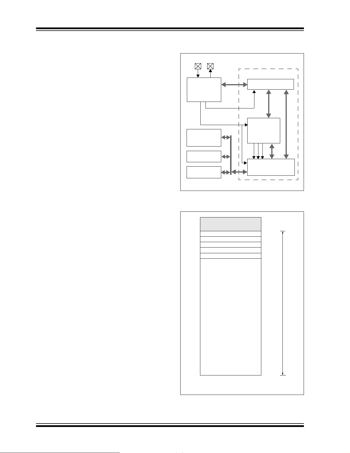
BOOTLOADER FIRMWARE
Basic Operation Overview
An overview of the CAN bootloader’s operation is
shown in Figure 1. A CAN Message Identifier and data
is received through the CAN module. One bit in the
identifier is used to indicate whether to PUT or GET
data. Another is used to determine if the message is to
be interpreted as data to be programmed or bootloader
control information. Writing data automatically invokes
the appropriate function to write to memory (FLASH,
Data EEPROM, or Configuration Memory). Writing to
the Control registers sets the operation of the
bootloader.
The bootloader can be configured at build time to support one of two mutually exclusive modes of operation.
In P Mode (or Put-only) mode, the microcontroller only
accepts PUT commands, and never “talks back” to the
source. In PG Mode, both PUT and GET commands
are accepted, allowing the source to both read from
and write to the target’s memory.
A more detailed explanation is provided in subsequent
sections.
FIGURE 1: BOOTLOADER FUNCTIONAL
BLOCK DIAGRAM
TXRX
Bootloader Firmware
CAN
Module
(Msg Identifier)
Configuration
Data
CONTROL/DATA
PUT/GET
FLASH
Program
Memory
EE
Data
Memory
Memory
Control/Data Buffer
Bootloader
Control
Registers
D8
D0
Memory I/O
Logic
FIGURE 2: PROGRAM MEMORY MAP OF
THE PIC18F458
Boot Program
RESET Vector
High Priority Interrupt Vector
Low Priority Interrupt Vector
0000h
0200h
0208h
0218h
Memory Organization
Program Memory
User Memory Space
PROGRAM MEMORY USAGE
Currently, PIC18F devices reserve the first 512 bytes of
Program Memory as the boot block. Future devices
may expand this, depending on application requirements for these devices. This bootloader is designed to
occupy the current designated boot block of 512 bytes
(or 256 words) of memory using the recommended
options. Note, however, some compile time options can
grow the bootloader beyond the boot block. Figure 2
Note: Memory areas not shown to scale.
shows a memory map of the PIC18F458. The boot
area can be code protected to prevent accidental
overwriting of the boot program.
DS00247A-page 2 2003 Microchip Technology Inc.
7FFFh
Page 3

AN247
REMAPPED MEMORY AND VECTORS
Since the hardware RESET and interrupt vectors lie
within the boot area and cannot be edited if the block is
protected, they are remapped through software to the
nearest parallel locations outside the boot block.
Remapping is simply a branch for interrupts, so PIC18F
users should note an additional latency of 2 instruction
cycles to handle interrupts. Upon RESET, there are
some boot condition checks, so the RESET latency is
an additional 10 instruction cycles (as seen in the
example source code).
Notice the memory regions do not necessarily correlate
to the physical addresses in the device (see Figure 3).
For example, EEDATA is located at F00000h; however,
in the PIC18 device, EEDATA operates as a separate
module and is not located in the device memory map.
In addition, the regions only define where the bootloader operates and the type of memory that it operates
on. This should not be interpreted as meaning that
writable memory is available over the entire defined
memory areas.
FIGURE 3: BOOTLOADER MEMORY
REGIONS
Boot Program
(000h - 1FFh)
Program Memory
Config Memory
Unused
000000h
2FFFFFh
300000h
3FFFFFh
FIGURE 4: DATA MEMORY MAP
000h
EE Data
Memory
Boot Control Byte
XXXh
COMMUNICATION AND CONTROL PROTOCOL
From the functional view in Figure 1, the bootloader
looks and behaves like a hardware module. This is
mostly because the bootloader’s operation is dictated
by two “commands” derived from single bit values, as
well as a set of defined Control registers.
Basic Bootloader Commands
There are essentially two data control commands: PUT
and GET. These commands are implemented through
a single bit passed via the CAN Message Identifier field
(in this version, bit 1 of the 18-bit Extended Identifier
field); the command is PUT when the bit is ‘0’, and GET
when it is ‘1’. PUT or GET can operate on either a type
of memory or the Control register set. GET commands
are ignored if P-Mode is specified.
The CONTROL/DATA bit, also defined in the Identifier
field (in this version, bit 0 of the Extended Identifier),
indicates the destination of the frame data. When the
bit is ‘0’, the data is interpreted as Control register
content; when it is ‘1’, the data is programming data.
The bit assignments for PUT/GET and CONTROL/DATA
are arbitrary, and are defined by compile time definitions.
The user may change the locations of these bits in the
identifier as the application requires.
F00000h
EEPROM Data
FFFFFFh
Note: Memory areas not shown to scale.
Control Registers
There are eight Control registers, which represent the
maximum number of bytes that can be contained in the
data field of a single CAN frame. The registers are
shown in order in Figure 5.
FIGURE 5: CONTROL REGISTERS
DATA MEMORY USAGE
The last location in Data Memory of the device
(Figure 4) is reserved as a non-volatile Boot mode flag.
This location contains FFh by default, which indicates
Boot mode. Any other value in this location indicates
normal Execution mode.
2003 Microchip Technology Inc. DS00247A-page 3
Address Low
Address High
Address Upper
(Reserved)
Control Bits
Command
Data A
Data B
D0
D1
D2
D3
D4
D5
D6
D7
Page 4

AN247
The Control registers are:
• Address Low (D0): This contains the low order
byte of the address pointer.
• Address High (D1): This register contains the
middle byte of the address pointer.
• Address Upper (D2): This register contains the
high order byte of the address pointer.
• Reserved (D3): This register is reserved for
expanded addressing.
• Control Bits (D4): This register contains bits that
define the basic operation of the bootloader.
• Command (D5): This location contains the immediate bootloader command. This is available to
allow special functions.
• Data A and Data B (D6 and D7): These Data
registers are reserved for expansions of the
bootloader command set.
Address Information
Control registers, D0 through D2, contain a 24-bit
address which can point to anywhere in the device’s
address space. Figure 3 shows the defined regions.
Control Bits
The five control bits in register D4 define how the
bootloader functions at run time. They are:
• WRITE_UNLOCK: Set this bit to unlock write
operations. This bit is provided to insure any write
operations to memory are intentional. This bit is
automatically cleared after a RESET.
• ERASE_ONLY: Set this bit to allow erase opera-
tions on Program Memory, but not write operations. This is useful when it is only necessary to
erase a section of memory. The address must be
on a 64-byte boundary to erase.
• AUTO_ERASE: Set this bit to automatically erase
while writing to memory. On every 64-byte boundary, the bootloader will automatically erase before
writing. This is useful when writing large sequential blocks of data over old data in Program
Memory.
• AUTO_INC: Set this to automatically increment
the address after each write or read operation.
This is useful when writing large sequential blocks
of data.
• ACK: In PG mode, set this bit to force the bootloader to send Acknowledgement of every PUT
command received. An Acknowledgement is
simply an empty CAN frame. This is useful in systems that require fully synchronized flow between
the source and the target.
TABLE 1: SUMMARY OF CONTROL BITS (REGISTER D4)
Bit # Bit Name Description
0 WRITE_UNLOCK 0 = Prevent writing (default).
1 = Allow write to any memory.
1 ERASE_ONLY 0 = Allow write after erase (default).
1 = Don’t write after erase.
2 AUTO_ERASE 0 = Don’t automatically erase before writing.
1 = Erase if on 64-byte border, then write (default).
3AUTO_INC 0 = Update pointer manually.
1 = Increment pointer automatically after operation (default).
4ACK 0 = Don’t send Acknowledgement.
1 = Send an empty CAN frame after every PUT command (PG mode only)(default).
DS00247A-page 4 2003 Microchip Technology Inc.
Page 5

AN247
Command and Data
There are four commands defined to add functionality
and reliability to the bootloader. These are summarized
in Table 2. They are:
• NOP: No operation. This is supplied to allow
writing Control registers without issuing a
command.
• RESET: Reset the device via the RESET
instruction.
• INIT_CHK: Initialize the checksum and verify registers. This clears the internal 16-bit checksum
and clears the verify flags.
• CHK_RUN: Test the checksum and verify registers;
if valid, then clear the last location of EEPROM.
Data is passed through the Data registers in the
Control register set and added to the checksum;
the program checks for zero. The internal
self-verify flag is also tested for zero.
Note that these are not the only commands that may be
implemented. Users may expand on this basic set by
using the high order bits of register D4, or using combinations of bits to define an expanded command set.
Registers D5 through D7 may also be used to define
additional parameters in combination with commands.
The basic 8-register structure for control allows users
to expand the command sets to their own needs.
TABLE 2: SUMMARY OF SPECIAL COMMANDS (COMMAND REGISTER D5)
Command Code Description
NOP 00h No operation.
RESET 01h Issue a Software Reset to the device.
INIT_CHK 02h Initialize internal checksum and verify registers.
CHK_RUN 03h Test the checksum and verify, then clear the last location of EEPROM if valid.
All other commands 04h - FFh Undefined - operate as NOP.
BOOTLOADER DETAILS
Reading/Writing/Erasing Program Memory
For writing to FLASH Program Memory, the Control
register address must point to memory region 000000h
to 2FFFFFh. Read operations occur at the byte level.
Write operations are performed on multiples of 8 bytes
(one block), while erase operations are performed on
64 bytes (one row).
Writing is an immediate operation. When the PUT
“DATA” command is received, the address already
stored in the Control registers is decoded and the data
is written to the target’s Program Memory. Data is only
written if the write operation has been unlocked.
When writing Program Memory, the memory should be
erased first. Either the auto erase or erase only options
can be used to erase memory on every 64-byte border.
The default operation is that bits can only be cleared
when written to. An erase operation is the only action
that can be used to set bits in Program Memory. Thus,
if the bootloader protection bits are not set up in the
Configuration registers, operations on memory from
000h to 1FFh could partially or completely disable the
bootloader firmware.
User IDs (starting at address 200000h) are considered
to be part of Program Memory and are written and
erased like normal FLASH Program Memory.
Reading/Writing EEPROM Data Memory
For writing to EEPROM Data Memory, the Control register address must point to memory region F00000h to
FFFFFFh. Read and write operations occur at the byte
level. Write operations must be unlocked before any
write operation can take place.
Note that the last location of the Data Memory is used
as a boot flag. Writing anything other than FFh to the
last location indicates normal code execution.
Configuration Bits
PIC18F devices allow access to the device configuration bits (addresses starting at 300000h) during normal
operation. In the bootloader, the Control register
address must point to memory region 300000h to
3FFFFFh to provide Configuration Memory access.
Data is read one byte at a time and, unlike Program
Memory, is written one byte at a time. Since configuration bits are automatically erased before being written,
the erase control bit will have no affect on Configuration
Memory.
Having access to configuration settings is very powerful; it is also potentially very dangerous. For example,
assume that the system is designed to run in HS mode
with a 20 MHz crystal. If the bootloader changes the
oscillator setting to LP mode, the system will cease to
function - including the bootloader! Basically, the
system has been killed by improperly changing one bit.
2003 Microchip Technology Inc. DS00247A-page 5
Page 6
AN247
It is also important to note some configuration bits are
single direction bits in Normal mode; they can only be
changed to one state, and cannot be changed back.
The code protection bits in Configuration registers 5L
and 5H are a good example. If any type of code protection is enabled for a block, it cannot be disabled without
a device programmer. Essentially, the bootloader
cannot reverse code protection.
The Device ID (addresses 3FFFFEh and 3FFFFFh) is
also considered Program Memory. While they can be
accessed, however, they are read only and cannot be
altered.
Write Latency
When writing data, there is a specific time that the programming source must wait for to complete the programming operation. Fortunately, the CAN module
actually buffers received data; therefore, receiving can
actually overlap memory write operations (Figure 6). In
general, it takes about 2 ms for Program Memory write
operations, while EEDATA takes about 4 ms. Not all
PIC18F devices have the same time specifications, so
it is important to verify the write times for the specific
device to be used.
FIGURE 6: CAN RECEIVE VS.
MEMORY WRITE
CAN
Message
Receive
Memory
Write
CAN
Msg
Writing in Assembly
When writing in assembly, the boot block and new vectors must be considered. For modular code, this is generally just a matter of changing the linker script file for
the project. An example is given in Appendix C. If an
absolute address is assigned to a code section, the
address must point somewhere above the boot block.
For those who write absolute assembly, all that is necessary to remember is that the new RESET vector is at
200h, and the interrupt vectors are at 208h and 218h.
No code except the bootloader should reside in the
boot block.
Writing in C
When using the MPLAB® C18 C compiler to develop
PIC18F firmware for an application, the standard
start-up object (c018.o or c018i.o) must be rebuilt
with the new RESET vector. Like modular assembly,
the linker file must be changed to incorporate the protected boot block and new vectors. Appendix C shows
an example linker file.
Users of other compilers should check with the compiler’s software user guide to determine how to change
the start-up code and vectors.
Bootloader Re-Entry
If the need exists to re-enter Boot mode from the application (and it usually does), the last location of the data
EEPROM must be set to FFh. The code in Example 1
demonstrates how this might be done in an application.
Since the bootloader assumes RESET conditions, a
RESET instruction should be initiated after setting the
last location.
WRITING CODE
The bootloader operates as a separate entity, which
means that an application can be developed with very
little concern about what the bootloader is doing. This
is as it should be; the bootloader should be dormant
code until an event initiates a boot operation. Under
ideal circumstances, bootloader code should never be
running during an application’s intended normal
operation.
When developing an application with a resident
bootloader, some basic principles must be kept in mind.
DS00247A-page 6 2003 Microchip Technology Inc.
EXAMPLE 1: SETTING THE LAST
LOCATION OF THE
DATA MEMORY
SETF EEADR ; Point to the last byte
SETF EEADRH
SETF EEDATA ; Bootmode control byte
MOVLW b'00000100 ; Setup for EEData
MOVWF EECON1
MOVLW 0x55 ; Unlock
MOVWF EECON2
MOVLW 0xAA
MOVWF EECON2
BSF EECON1, WR ; Start the write
NOP
BTFSC EECON1, WR ; Wait
BRA $ - 2
RESET
Page 7

AN247
Debugging
For most situations, it is not necessary to have the
bootloader firmware in memory to do debugging of an
application with either the MPLAB ICD 2 or ICE
devices. However, branch statements must be inserted
at the hardware vectors to get to the new designated
vectors. It may also be useful to have the start-up timing match exactly to the bootloader entry. When development of the application is finished, either remove the
branches and rebuild the project, or export only the
memory above the boot block. This code can then be
distributed to those who are updating their firmware.
COMPILE TIME OPTIONS
Compile time options are available to provide initial settings as well as features. Some features require more
memory than others. Compiling certain combinations of
options can actually generate code that is larger than
the designated boot block.
Modes of Operation (Compile Time)
The bootloader can be built to support either one of two
mutually exclusive modes of operation:
• P Mode - Only PUT commands are accepted. The
device will never ‘talk back’ to the source.
• PG Mode - Both PUT and GET are allowed. The
source can actually read out of the target’s
memory as well as write to the target’s memory.
The compile time definition, ALLOW_GET_CMD, selects
the mode.
Self-Verification
The definition, MODE_SELF_VERIFY, enables a
self-verification feature. With this feature, the firmware
reads back the data written to any type of memory (not
Control registers), and it compares the read data with
the source (received) data. A flag is set in a register if
verification failed.
Vectors
The RESET and interrupt vectors can be set to any
location using the following definitions:
• RESET_VECT
• HIGH_INT_VECT
• LOW_INT_VECT
The default values reside at addresses 200h, 208h,
and 218h, outside of the boot block; they parallel the
default PIC18F458 interrupt vectors. If compiling some
features causes the bootloader to be larger than the
boot block, then these vectors must be adjusted to
addresses above the used memory area. If the jump is
farther than a relative branch, then the definition,
NEAR_JUMP, must be removed.
Other Basic Settings
There are several other definitions that set CAN
specific settings. These determine which bits of the
message identifier are used for the PUT/GET and
CONTROL/DATA commands, the CONTROL/DATA bit
used for GET responses, as well as the filters and
masks for the programming node. Refer to Table 3 for
specific details.
2003 Microchip Technology Inc. DS00247A-page 7
Page 8

AN247
TABLE 3: SUMMARY OF COMPILE TIME DEFINITIONS
Definition
ALLOW_GET_CMD N/A Allows GET commands. If not present, then the bootloader will only
MODE_SELF_VERIFY N/A Enables self-verification of data written to memory.
NEAR_JUMP N/A Uses BRA to jump to vectors. If not defined, then it uses GOTO.
HIGH_INT_VECT 208h Remapped high priority interrupt vector.
LOW_INT_VECT 218h Remapped low priority interrupt vector.
RESET_VECT 200h Remapped RESET vector.
CAN_CD_BIT RXB0EIDL<0> Received CONTROL/DATA select bit.
CAN_PG_BIT RXB0EIDL<1> Received PUT/GET select bit.
CANTX_CD_BIT TXB0EIDL<0> Transmitted CONTROL/DATA select bit.
CAN_TXB0SIDH 10000000 Transmitted identifier for target node.
CAN_TXB0SIDL 00001000
CAN_TXB0EIDH 00000000
CAN_TXB0EIDL 00000100
CAN_RXF0SIDH 00000000 Receive filter for target node.
CAN_RXF0SIDL 00001000
CAN_RXF0EIDH 00000000
CAN_RXF0EIDL 00000111
CAN_RXM0SIDH 11111111 Receive mask for target node.
CAN_RXM0SIDL 11100011
CAN_RXM0EIDH 11111111
CAN_RXM0EIDL 11111100
CAN_BRGCON1 11000001 CAN bit rate control.
CAN_BRGCON2 10111010
CAN_BRGCON3 00000111
CAN_CIOCON 00100000 CAN I/O control.
Value
(Default)
Description
receive CAN messages.
DS00247A-page 8 2003 Microchip Technology Inc.
Page 9

AN247
TIPS FOR SUCCESSFUL FIELD PROGRAMMING
Successful programming can take several forms,
depending on which compile time options are selected.
In P-Mode with self-verification enabled, the programmed target keeps a running 16-bit sum of all the
data written to memory. In addition, every write operation is verified by reading back and comparing the data,
providing some assurance that all data was received
and that all data was correctly written.
In PG mode without self-verification, the programming
source can read as well as write data. Thus, verification
is provided directly by the source.
EXAMPLE PROGRAMMING SEQUENCE (P MODE)
1. Put the programming target in Boot mode.
2. Send a control packet. Load the address with
the beginning memory. Unlock write operations.
Enable auto erase. Disable erase only. Issue a
Self-Verify Reset.
3. Send Program Memory data. The data must be
8 bytes and aligned on an even 8-byte address.
4. Wait an appropriate amount of time.
5. Repeat steps 3 and 4 until all Program Memory
is written.
6. Send EEPROM Data Memory data.
7. Wait an appropriate amount of time.
8. Repeat steps 6 and 7 until all EEPROM Data
Memory is written except for the last location.
9. Send one byte of Configuration Memory data.
10. Wait an appropriate amount of time.
11. Repeat steps 9 and 10 until all the desired con-
figuration settings are written. If setting memory
protection, write these last.
12. Send a control packet. Send a check and run
command. Also, send the two’s compliment of
the sum of all data written in the Data registers
in the same packet.
13. Send a RESET command. If self-verification suc-
ceeded, then the node should be running the new
application. This could be verified at the application level by the programming source, or any
other node in the network that communicates
with the target.
EXAMPLE PROGRAMMING SEQUENCE (PG MODE)
1. Put the programming target in Boot mode.
2. Send a control packet. Load the address with
the beginning memory. Unlock write operations.
Enable auto erase. Disable erase only.
3. Send Program Memory data. The data must be
8 bytes and aligned on an even 8-byte address.
4. Wait an appropriate amount of time.
5. Read back the data written and compare. If fail,
then reset the pointer and try again, steps 3
and 4.
6. Repeat steps 3, 4, and 5 until all Program
Memory is written.
7. Send EEPROM Data Memory data.
8. Wait an appropriate amount of time.
9. Read back the data written and compare. If fail,
then reset the pointer and try again, steps 7
and 8.
10. Repeat steps 7, 8, and 9 until all EEPROM Data
Memory is written except for the last location.
11. Send one byte of Configuration Memory data.
12. Wait an appropriate amount of time.
13. Read back the data written and compare. If fail,
then reset the pointer and try again, steps 11
and 12.
14. Repeat steps 11, 12, and 13 until all the desired
configuration settings are written. If setting
memory protection, write these last.
15. Write 00h to the last location of EEPROM Data
Memory.
16. Send a RESET command. Functionality should
be verified at the application level by the
programming source, or any other node in the
network that communicates with the target.
2003 Microchip Technology Inc. DS00247A-page 9
Page 10

AN247
RESOURCES
For most builds, the PIC18F CAN bootloader resides
within the device’s Boot Block (000h to 1FFh), and
does not impact the normal Program Memory space
beyond the relocation of the interrupt vectors.
As noted, some combinations of compile time options
(for example, selecting both PG mode and self-verify)
will result in a bootloader that exceeds the Boot Block
size. In these cases, it will be necessary to relocate any
user application code and the interrupt vectors above
the boundary of the bootloader, being careful to avoid
code overlap. If Program Memory space is not critical,
the optimal solution may be to locate all application
code and the interrupt vectors above the upper boundary of Block 0 (1FFFh). Write protecting Block 0 to
protect the bootloader is desirable, but not essential.
The bootloader uses 12 bytes of data SRAM during
operation. It also uses 1 byte of data EEPROM at all
times, as the normal operation/bootloader flag.
REFERENCES
W. L awren z, CAN System Engineering From Theory to
Practical Applications. New York: Springer-Verlag
New York Inc., 1997.
MPLAB-CXX Compiler User’s Guide, Microchip
Technology Inc., 2000 (Document number DS51217).
Microchip Technology Inc., Application Note AN851, “A
FLASH Bootloader for PIC16 and PIC18 Devices”
(Document number DS00851).
DS00247A-page 10 2003 Microchip Technology Inc.
Page 11

AN247
APPENDIX A: A SIMPLE
PROGRAMMING
INTERFACE
To demonstrate the functionality of the CAN bootloader,
a simple serial-to-CAN interface is discussed briefly
here. The hardware, controller firmware and software
are designed to work as a package. Users are encouraged to use this design example as a starting point for
developing their own programming systems.
The Hardware
An underlying assumption of the bootloader is that
some method exists to introduce the new program data
to the target CAN network. There may be cases, however, where no provision has been made for a network
to communicate with an outside data source. In these
cases, it is necessary to introduce a CAN node whose
sole function is to provide an external data interface.
A schematic outline for the interface’s hardware is presented in Figure A-1 and Figure A-2 (following pages).
The heart of the design is a PIC18F458 microcontroller,
which runs the programming firmware and provides
both CAN and RS-232 communications. Interfaces to
the CAN bus and programming data source are provided by an external CAN transceiver and RS-232
interface.
Optional status LEDs, headers for accessing the controller’s I/O ports and power regulation are provided in
the design. These may be modified, removed or
expanded upon as the system design requires.
The Firmware
The firmware is an extension of the PIC18F serial bootloader discussed in Microchip Application Note AN851,
“A FLASH Bootloader for PIC16 and PIC18 Devices”.
Two new commands (RD_SRAM and WT_SRAM) have
been added to provide access to SRAM, thus allowing
complete control of all the peripherals (including the
CAN module) through the serial bootloader.
A summary of the commands and syntax for the PIC18
FLASH Bootloader is provided in Appendix A of
Application Note AN851.
The Host Software
The software portion of the interface is designed to run
on IBM
Windows®. It provides a simple graphic-based tool to
translate program files in Intel
data for the programmer firmware.
THE CANCOMM CONTROL
The software interface uses an ActiveX® control to provide simple communications with the CAN module
through the serial port. For those who wish to experiment with the interface, a total of 4 properties and 13
methods are available to the user. These are listed in
Table A-1.
THE USER INTERFACE
A simple graphic and text interface allows the user to
keep track of the bootloading operations in real-time.
Examples of the interface’s dialogs are shown in
Figure A-3.
®
compatible computers running Microsoft
®
HEX format into serial
®
TABLE A-1: ActiveX METHODS USED BY THE HOST SOFTWARE
Method Type Purpose
BitRate Property Sets the bit rate of the comm port.
CommPort Property Specifies the comm port.
MaxTimeOut Property Specifies the maximum wait (in milliseconds) for data to be received in
the computer’s serial buffer.
MaxRetrys Property Specifies the maximum number of times to resend a serial packet.
SetFilter Method Sets a CAN filter on the interface.
SetMask Method Sets a CAN mask on the interface.
GetMsg Method Gets the message from the CAN receive buffer.
PutMsg Method Puts the message in the CAN transmit buffer.
SetBitRate Method Sets the CAN bit rate.
Init Method Initializes the CAN module on the interface.
IsGetMsgRdy Method Determines if the receive buffer has data.
IsPutMsgRdy Method Determines if the transmit buffer is open.
GoOnBus Method Puts the interface on the CAN bus.
GoOffBus Method Takes the interface off the CAN bus.
GetStat Method Gets the current status of the interface CAN module.
OpenComm Method Opens serial communications to the interface
CloseComm Method Closes communications to the CAN interface.
2003 Microchip Technology Inc. DS00247A-page 11
Page 12

AN247
FIGURE A-1: BOOTLOADER HARDWARE INTERFACE FOR CAN NETWORKS
(MCU AND SERIAL INTERFACES)
PIC18F458/PT
DS00247A-page 12 2003 Microchip Technology Inc.
Page 13

FIGURE A-2: BOOTLOADER HARDWARE INTERFACE FOR CAN NETWORKS
(POWER SUPPLY, DISPLAYS AND CONNECTION HEADERS)
AN247
2003 Microchip Technology Inc. DS00247A-page 13
Page 14

AN247
FIGURE A-3: EXAMPLE DIALOGS FOR THE CANCOMM HOST SOFTWARE:
OUTPUT STATUS MESSAGES (TOP) AND PROGRESS BAR (BOTTOM)
DS00247A-page 14 2003 Microchip Technology Inc.
Page 15

AN247
Software License Agreement
The software supplied herewith by Microchip Technology Incorporated (the “Company”) is intended and supplied to you, the
Company’s customer, for use solely and exclusively with products manufactured by the Company.
The software is owned by the Company and/or its supplier, and is protected under applicable copyright laws. All rights are reserved.
Any use in violation of the foregoing restrictions may subject the user to criminal sanctions under applicable laws, as well as to civil
liability for the breach of the terms and conditions of this license.
THIS SOFTWARE IS PROVIDED IN AN “AS IS” CONDITION. NO WARRANTIES, WHETHER EXPRESS, IMPLIED OR STATUTORY, INCLUDING, BUT NOT LIMITED TO, IMPLIED WARRANTIES OF MERCHANTABILITY AND FITNESS FOR A PARTICULAR PURPOSE APPLY TO THIS SOFTWARE. THE COMPANY SHALL NOT, IN ANY CIRCUMSTANCES, BE LIABLE FOR
SPECIAL, INCIDENTAL OR CONSEQUENTIAL DAMAGES, FOR ANY REASON WHATSOEVER.
APPENDIX B: CAN BOOTLOADER FIRMWARE
;*****************************************************************************
;*
;* Microchip CAN Bootloader
;*
;*****************************************************************************
;* FileName: CANIO.asm
;* Dependencies:
;* Processor: PIC18F with CAN
;* Assembler: MPASMWIN 03.10.04 or higher
;* Linker: MPLINK 03.10.04 or higher
;* Company: Microchip Technology Incorporated
;*
;* Basic Operation:
;* The following is a CAN bootloader designed for PIC18F microcontrollers
;* with built-in CAN such as the PIC18F458. The bootloader is designed to
;* be simple, small, flexible, and portable.
;*
;* The bootloader can be compiled for one of two major modes of operation:
;*
;* PG Mode: In this mode the bootloader allows bi-directional communication
;* with the source. Thus the bootloading source can query the
;* target and verify the data being written.
;*
;* P Mode: In this mode the bootloader allows only single direction
;* communication, i.e. source -> target. In this mode programming
;* verification is provided by performing self verification and
;* checksum of all written data (except for control data).
;*
;* The bootloader is essentially a register-controlled system. The control
;* registers hold information that dictates how the bootloader functions.
;* Such information includes a generic pointer to memory, control bits to
;* assist special write and erase operations, and special command registers
;* to allow verification and release of control to the main application.
;*
;* After setting up the control registers, data can be sent to be written
;* to or a request can be sent to read from the selected memory defined by
;* the address. Depending on control settings the address may or may not
;* automatically increment to the next address.
;*
;* Commands:
;* Put commands received from source (Master --> Slave)
;* The count (DLC) can vary.
;* XXXXXXXXXXX 0 0 8 XXXXXXXX XXXXXX00 ADDRL ADDRH ADDRU RESVD CTLBT SPCMD CPDTL CPDTH
;* XXXXXXXXXXX 0 0 8 XXXXXXXX XXXXXX01 DATA0 DATA1 DATA2 DATA3 DATA4 DATA5 DATA6 DATA7
;*
;* The following response commands are only used for PG mode.
;* Get commands received from source (Master --> Slave)
;* Uses control registers to get data. Eight bytes are always assumed.
;* XXXXXXXXXXX 0 0 0 XXXXXXXX XXXXXX10 _NA__ _NA__ _NA__ _NA__ _NA__ _NA__ _NA__ _NA__
;* XXXXXXXXXXX 0 0 0 XXXXXXXX XXXXXX11 _NA__ _NA__ _NA__ _NA__ _NA__ _NA__ _NA__ _NA__
2003 Microchip Technology Inc. DS00247A-page 15
Page 16

AN247
;*
;* Put commands sent upon receiving Get command (Slave --> Master)
;* YYYYYYYYYYY 0 0 8 YYYYYYYY YYYYYY00 ADDRL ADDRH ADDRU RESVD STATS RESVD RESVD RESVD
;* YYYYYYYYYYY 0 0 8 YYYYYYYY YYYYYY01 DATA0 DATA1 DATA2 DATA3 DATA4 DATA5 DATA6 DATA7
;*
;* Put commands sent upon receiving Put command (if enabled) (Slave --> Master)
;* This is the acknowledge after a put.
;* YYYYYYYYYYY 0 0 0 YYYYYYYY YYYYYY00 _NA__ _NA__ _NA__ _NA__ _NA__ _NA__ _NA__ _NA__
;* YYYYYYYYYYY 0 0 0 YYYYYYYY YYYYYY01 _NA__ _NA__ _NA__ _NA__ _NA__ _NA__ _NA__ _NA__
;*
;* ADDRL - Bits 0 to 7 of the memory pointer.
;* ADDRH - Bits 8 - 15 of the memory pointer.
;* ADDRU - Bits 16 - 23 of the memory pointer.
;* RESVD - Reserved for future use.
;* CTLBT - Control bits.
;* SPCMD - Special command.
;* CPDTL - Bits 0 - 7 of special command data.
;* CPDTH - Bits 8 - 15 of special command data.
;* DATAX - General data.
;*
;* Control bits:
;* MODE_WRT_UNLCK-Set this to allow write and erase operations to memory.
;* MODE_ERASE_ONLY-Set this to only erase Program Memory on a put command. Must be on 64-byte
;* boundary.
;* MODE_AUTO_ERASE-Set this to automatically erase Program Memory while writing data.
;* MODE_AUTO_INC-Set this to automatically increment the pointer after writing.
;* MODE_ACK-Set this to generate an acknowledge after a 'put' (PG Mode only)
;*
;* Special Commands:
;* CMD_NOP 0x00 Do nothing
;* CMD_RESET 0x01 Issue a soft reset
;* CMD_RST_CHKSM 0x02 Reset the checksum counter and verify
;* CMD_CHK_RUN 0x03 Add checksum to special data, if verify and zero checksum
;* then clear the last location of EEDATA.
;* Memory Organization (regions not shown to scale):
;* |-------------------------------|0x000000 (Do not write here!)
;* | Boot Area |
;* |-------------------------------|0x000200
;* | |
;* | Prog Mem |
;* | |
;* |-------------------------------|0x1FFFFF
;* | User ID |0x200000
;* |-------------------------------|
;* |:::::::::::::::::::::::::::::::|
;* |:::::::::::::::::::::::::::::::|
;* |-------------------------------|
;* | Config |0x300000
;* |-------------------------------|
;* |:::::::::::::::::::::::::::::::|
;* |:::::::::::::::::::::::::::::::|
;* |-------------------------------|
;* | Device ID |0x3FFFFE - 0x3FFFFF
;* |-------------------------------|
;* |:::::::::::::::::::::::::::::::|
;* |:::::::::::::::::::::::::::::::|
;* |-------------------------------|0xF00000
;* | EEDATA |
;* | (remapped) |(Last byte used as boot flag)
;* |-------------------------------|0xFFFFFF
;
DS00247A-page 16 2003 Microchip Technology Inc.
Page 17

;* Author Date Comment
;*~~~~~~~~~~~~~~~~~~~~~~~~~~~~~~~~~~~~~~~~~~~~~~~~~~~~~~~~~~~~~~~~~~~~~~~~~~~~
;* Ross Fosler 11/26/02 First full revision
;*
;*****************************************************************************/
; *****************************************************************************
#include p18cxxx.inc
#include canio.def
; *****************************************************************************
; *****************************************************************************
#ifndef EEADRH
#define EEADRH EEADR+1
#endif
#define TRUE 1
#define FALSE 0
#define WREG1 PRODH ; Alternate working register
#define WREG2 PRODL
#define MODE_WRT_UNLCK _bootCtlBits,0 ; Unlock write and erase
#define MODE_ERASE_ONLY_bootCtlBits,1 ; Erase without write
#define MODE_AUTO_ERASE_bootCtlBits,2 ; Enable auto erase before write
#define MODE_AUTO_INC _bootCtlBits,3 ; Enable auto inc the address
#define MODE_ACK _bootCtlBits,4 ; Acknowledge mode
#define ERR_VERIFY _bootErrStat,0 ; Failed to verify
#define CMD_NOP 0x00
#define CMD_RESET 0x01
#define CMD_RST_CHKSM 0x02
#define CMD_CHK_RUN 0x03
; *****************************************************************************
AN247
; *****************************************************************************
_MEM_IO_DATA UDATA_ACS 0x00
; *****************************************************************************
_bootCtlMem
_bootAddrL RES 1 ; Address info
_bootAddrH RES 1
_bootAddrU RES 1
_unused0 RES 1 ; (Reserved)
_bootCtlBits RES 1 ; Boot Mode Control bits
_bootSpcCmd RES 1 ; Special boot commands
_bootChkL RES 1 ; Special boot command data
_bootChkH RES 1
_bootCount RES 1
_bootChksmL RES 1 ; 16 bit checksum
_bootChksmH RES 1
_bootErrStat RES 1 ; Error Status flags
; *****************************************************************************
2003 Microchip Technology Inc. DS00247A-page 17
Page 18

AN247
; *****************************************************************************
_STARTUPCODE 0x00
; *****************************************************************************
bra _CANInit
bra _StartWrite
; *****************************************************************************
_INTV_H CODE 0x08
; *****************************************************************************
#ifdef NEAR_JUMP
bra HIGH_INT_VECT
#else
goto HIGH_INT_VECT
#endif
; *****************************************************************************
_INTV_L CODE 0x18
; *****************************************************************************
#ifdef NEAR_JUMP
bra LOW_INT_VECT
#else
goto LOW_INT_VECT
#endif
; *****************************************************************************
; *****************************************************************************
_CAN_IO_MODULE CODE
; *****************************************************************************
; Function: VOID _StartWrite(WREG _eecon_data)
;
; PreCondition: Nothing
; Input: _eecon_data
; Output: Nothing. Self write timing started.
; Side Effects: EECON1 is corrupted; WREG is corrupted.
; Stack Requirements: 1 level.
; Overview: Unlock and start the write or erase sequence to protected
; memory. Function will wait until write is finished.
;
; *****************************************************************************
_StartWrite:
movwf EECON1
btfss MODE_WRT_UNLCK ; Stop if write locked
return
movlw 0x55 ; Unlock
movwf EECON2
movlw 0xAA
movwf EECON2
bsf EECON1, WR ; Start the write
nop
btfsc EECON1, WR ; Wait (depends on mem type)
bra $ - 2
return
; *****************************************************************************
DS00247A-page 18 2003 Microchip Technology Inc.
Page 19

; *****************************************************************************
; Function: _bootChksm _UpdateChksum(WREG _bootChksmL)
;
; PreCondition: Nothing
; Input: _bootChksmL
; Output: _bootChksm. This is a static 16 bit value stored in the Access Bank.
; Side Effects: STATUS register is corrupted.
; Stack Requirements: 1 level.
; Overview: This function adds a byte to the current 16 bit checksum
; count. WREG should contain the byte before being called.
;
; The _bootChksm value is considered a part of the special
; register set for bootloading. Thus it is not visible.
;
;***************************************************************************
_UpdateChksum:
addwf _bootChksmL, F ; Keep a checksum
btfsc STATUS, C
incf _bootChksmH, F
return
; *****************************************************************************
; *****************************************************************************
; Function: VOID _CANInit(CAN, BOOT)
;
; PreCondition: Enter only after a reset has occurred.
; Input: CAN control information, bootloader control information
; Output: None.
; Side Effects: N/A. Only run immediately after reset.
; Stack Requirements: N/A
; Overview: This routine is technically not a function since it will not
; return when called. It has been written in a linear form to
; save space.Thus 'call' and 'return' instructions are not
; included, but rather they are implied.
;
; This routine tests the boot flags to determine if boot mode is
; desired or normal operation is desired. If boot mode then the
; routine initializes the CAN module defined by user input. It
; also resets some registers associated to bootloading.
;
; *****************************************************************************
_CANInit:
clrf EECON1
setf EEADR ; Point to last location of EEDATA
setf EEADRH
bsf EECON1, RD ; Read the control code
incfsz EEDATA, W
AN247
#ifdef NEAR_JUMP
bra RESET_VECT ; If not 0xFF then normal reset
#else
goto RESET_VECT
#endif
clrf _bootSpcCmd ; Reset the special command register
movlw 0x1C ; Reset the boot control bits
movwf _bootCtlBits
movlb d'15' ; Set Bank 15
bcf TRISB, CANTX ; Set the TX pin to output
movlw CAN_RXF0SIDH ; Set filter 0
movwf RXF0SIDH
movlw CAN_RXF0SIDL
movwf RXF0SIDL
comf WREG ; Prevent filter 1 from causing a
2003 Microchip Technology Inc. DS00247A-page 19
Page 20

AN247
movwf RXF1SIDL ; receive event
movlw CAN_RXF0EIDH
movwf RXF0EIDH
movlw CAN_RXF0EIDL
movwf RXF0EIDL
movlw CAN_RXM0SIDH ; Set mask
movwf RXM0SIDH
movlw CAN_RXM0SIDL
movwf RXM0SIDL
movlw CAN_RXM0EIDH
movwf RXM0EIDH
movlw CAN_RXM0EIDL
movwf RXM0EIDL
movlw CAN_BRGCON1 ; Set bit rate
movwf BRGCON1
movlw CAN_BRGCON2
movwf BRGCON2
movlw CAN_BRGCON3
movwf BRGCON3
movlw CAN_CIOCON ; Set IO
movwf CIOCON
clrf CANCON ; Enter Normal mode
; *****************************************************************************
; *****************************************************************************
; This routine is essentially a polling loop that waits for a
; receive event from RXB0 of the CAN module. When data is
; received, FSR0 is set to point to the TX or RX buffer depending
; upon whether the request was a 'put' or a 'get'.
; *****************************************************************************
_CANMain:
bcf RXB0CON, RXFUL ; Clear the receive flag
btfss RXB0CON, RXFUL ; Wait for a message
bra $ - 2
clrwdt
#ifdef ALLOW_GET_CMD
btfss CAN_PG_BIT ; Put or get data?
bra _CANMainJp1
lfsr 0, TXB0D0 ; Set pointer to the transmit buffer
movlw 0x08
movwf _bootCount ; Setup the count to eight
movwf WREG1
bra _CANMainJp2
#endif
_CANMainJp1
lfsr 0, RXB0D0 ; Set pointer to the receive buffer
movf RXB0DLC, W
andlw 0x0F
movwf _bootCount ; Store the count
movwf WREG1
bz _CANMain ; Go back if no data specified for a put
_CANMainJp2
; *****************************************************************************
DS00247A-page 20 2003 Microchip Technology Inc.
Page 21

; *****************************************************************************
; Function: VOID _ReadWriteMemory()
;
; PreCondition:Enter only after _CANMain().
; Input: None.
; Output: None.
; Side Effects: N/A.
; Stack Requirements: N/A
; Overview: This routine is technically not a function since it will not
; return when called. It has been written in a linear form to
; save space.Thus 'call' and 'return' instructions are not
; included, but rather they are implied.
;
; This is the memory I/O engine. A total of eight data
; bytes are received and decoded. In addition two control
; bits are received, put/get and control/data.
;
; A pointer to the buffer is passed via FSR0 for reading or writing.
;
; The control register set contains a pointer, some control bits
; and special command registers.
;
; Control
; <PG><CD><ADDRL><ADDRH><ADDRU><_RES_><CTLBT><SPCMD><CPDTL><CPDTH>
;
; Data
; <PG><CD><DATA0><DATA1><DATA2><DATA3><DATA4><DATA5><DATA6><DATA7>
;
; PG bit: Put = 0, Get = 1
; CD bit: Control = 0, Data = 1
;
; *****************************************************************************
_ReadWriteMemory:
btfscCAN_CD_BIT ; Write/read data or control registers
bra _DataReg
AN247
; *****************************************************************************
; This routine reads or writes the bootloader control registers,
; then executes any immediate command received.
_ControlReg
lfsr 1, _bootCtlMem
_ControlRegLp1
#ifdef ALLOW_GET_CMD
btfsc CAN_PG_BIT ; or copy control registers to buffer
movff POSTINC1, POSTINC0
btfss CAN_PG_BIT ; Copy the buffer to the control registers
#endif
movff POSTINC0, POSTINC1
decfsz WREG1, F
bra _ControlRegLp1
#ifdef ALLOW_GET_CMD
btfsc CAN_PG_BIT
bra _CANSendResponce; Send response if get
#endif
; *********************************************************
; This is a no operation command.
movf _bootSpcCmd, W; NOP Command
bz _SpecialCmdJp2; or send an acknowledge
; *********************************************************
2003 Microchip Technology Inc. DS00247A-page 21
Page 22

AN247
; *********************************************************
; This is the reset command.
xorlw CMD_RESET ; RESET Command
btfsc STATUS, Z
reset
; *********************************************************
; This is the Selfcheck reset command. This routine
; resets the internal check registers, i.e. checksum and
; self verify.
movf _bootSpcCmd, W ; RESET_CHKSM Command
xorlw CMD_RST_CHKSM
bnz _SpecialCmdJp1
clrf _bootChksmH ; Reset chksum
clrf _bootChksmL
bcf ERR_VERIFY ; Clear the error verify flag
; *********************************************************
; This is the Test and Run command. The checksum is
; verified, and the self-write verification bit is checked.
; If both pass, then the boot flag is cleared.
_SpecialCmdJp1
movf _bootSpcCmd, W ; RUN_CHKSM Command
xorlw CMD_CHK_RUN
bnz _SpecialCmdJp2
movf _bootChkL, W ; Add the control byte
addwf _bootChksmL, F
bnz _SpecialCmdJp2
movf _bootChkH, W
addwfc _bootChksmH, F
bnz _SpecialCmdJp2
btfsc ERR_VERIFY ; Look for verify errors
bra _SpecialCmdJp2
setf EEADR ; Point to last location of EEDATA
setf EEADRH
clrf EEDATA ; and clear the data
movlw b'00000100' ; Setup for EEData
rcall _StartWrite
_SpecialCmdJp2
#ifdef ALLOW_GET_CMD
bra _CANSendAck ; or send an acknowledge
#else
bra _CANMain
#endif
; *****************************************************************************
DS00247A-page 22 2003 Microchip Technology Inc.
Page 23

; *****************************************************************************
; This is a jump routine to branch to the appropriate memory access function.
; The high byte of the 24-bit pointer is used to determine which memory to access.
; All program memories (including Config and User IDs) are directly mapped.
; EEDATA is remapped.
_DataReg
; *********************************************************
_SetPointers
movf _bootAddrU, W ; Copy upper pointer
movwf TBLPTRU
andlw 0xF0 ; Filter
movwf WREG2
movf _bootAddrH, W ; Copy the high pointer
movwf TBLPTRH
movwf EEADRH
movf _bootAddrL, W ; Copy the low pointer
movwf TBLPTRL
movwf EEADR
btfss MODE_AUTO_INC ; Adjust the pointer if auto inc is enabled
bra _SetPointersJp1
movf _bootCount, W ; add the count to the pointer
addwf _bootAddrL, F
clrf WREG
addwfc _bootAddrH, F
addwfc _bootAddrU, F
_SetPointersJp1
AN247
_Decode
movlw 0x30 ; Program memory < 0x300000
cpfslt WREG2
bra _DecodeJp1
#ifdef ALLOW_GET_CMD
btfsc CAN_PG_BIT
bra _PMRead
#endif
bra _PMEraseWrite
_DecodeJp1
movf WREG2,W ; Config memory = 0x300000
xorlw 0x30
bnz _DecodeJp2
#ifdef ALLOW_GET_CMD
btfsc CAN_PG_BIT
bra _PMRead
#endif
bra _CFGWrite
_DecodeJp2
movf WREG2,W ; EEPROM data = 0xF00000
xorlw 0xF0
bnz _CANMain
#ifdef ALLOW_GET_CMD
btfsc CAN_PG_BIT
bra _EERead
#endif
bra _EEWrite
; *****************************************************************************
2003 Microchip Technology Inc. DS00247A-page 23
Page 24

AN247
; *****************************************************************************
; Function: VOID _PMRead()
; VOID _PMEraseWrite()
;
; PreCondition:WREG1 and FSR0 must be loaded with the count and address of
; the source data.
; Input: None.
; Output: None.
; Side Effects: N/A.
; Stack Requirements: N/A
; Overview: These routines are technically not functions since they will not
; return when called. They have been written in a linear form to
; save space.Thus 'call' and 'return' instructions are not
; included, but rather they are implied.
;
; These are the program memory read/write functions. Erase is
; available through control flags. An automatic erase option
; is also available. A write lock indicator is in place to
; ensure intentional write operations.
;
; Note: write operations must be on 8-byte boundaries and
; must be 8 bytes long. Also erase operations can only
; occur on 64-byte boundaries.
;
; *****************************************************************************
#ifdef ALLOW_GET_CMD
_PMRead:
tblrd*+ ; Fill the buffer
movff TABLAT, POSTINC0
decfsz WREG1, F
bra _PMRead ; Not finished then repeat
bra _CANSendResponce
#endif
_PMEraseWrite:
btfss MODE_AUTO_ERASE ; Erase if auto erase is requested
bra _PMWrite
_PMErase:
movf TBLPTRL, W ; Check for a valid 64 byte border
andlw b'00111111'
bnz _PMWrite
_PMEraseJp1
movlw b'10010100' ; Setup erase
rcall _StartWrite ; Erase the row
_PMWrite:
btfsc MODE_ERASE_ONLY ; Don't write if erase only is requested
#ifdef ALLOW_GET_CMD
bra _CANSendAck
#else
bra _CANMain
#endif
movf TBLPTRL, W ; Check for a valid 8 byte border
andlw b'00000111'
bnz _CANMain
movlw 0x08
movwf WREG1
DS00247A-page 24 2003 Microchip Technology Inc.
Page 25

_PMWriteLp1
movf POSTINC0, W ; Load the holding registers
movwf TABLAT
rcall _UpdateChksum ; Adjust the checksum
tblwt*+
decfsz WREG1, F
bra _PMWriteLp1
#ifdef MODE_SELF_VERIFY
movlw 0x08
movwf WREG1
_PMWriteLp2
tblrd*- ; Point back into the block
movf POSTDEC0, W
decfsz WREG1, F
bra _PMWriteLp2
movlw b'10000100' ; Setup writes
rcall _StartWrite ; Write the data
movlw 0x08
movwf WREG1
_PMReadBackLp1
tblrd*+ ; Test the data
movf TABLAT, W
xorwf POSTINC0, W
btfss STATUS, Z
bsf ERR_VERIFY
decfsz WREG1, F
bra _PMReadBackLp1 ; Not finished then repeat
#else
tblrd*- ; Point back into the block
movlw b'10000100' ; Setup writes
rcall _StartWrite ; Write the data
tblrd*+ ; Return the pointer position
#endif
AN247
#ifdef ALLOW_GET_CMD
bra _CANSendAck
#else
bra _CANMain
#endif
; *****************************************************************************
2003 Microchip Technology Inc. DS00247A-page 25
Page 26

AN247
; *****************************************************************************
; Function: VOID _CFGWrite()
; VOID _CFGRead()
;
; PreCondition:WREG1 and FSR0 must be loaded with the count and address of the source data.
; Input: None.
; Output: None.
; Side Effects: N/A.
; Stack Requirements: N/A
; Overview: These routines are technically not functions since they will not
; return when called. They have been written in a linear form to
; save space. Thus 'call' and 'return' instructions are not
; included, but rather they are implied.
;
; These are the Config memory read/write functions. Read is
; actually the same for standard program memory, so any read
; request is passed directly to _PMRead.
;
; *****************************************************************************
_CFGWrite:
#ifdef MODE_SELF_VERIFY ; Write to config area
movf INDF0, W ; Load data
#else
movf POSTINC0, W
#endif
movwf TABLAT
rcall _UpdateChksum ; Adjust the checksum
tblwt* ; Write the data
movlw b'11000100'
rcall _StartWrite
tblrd*+ ; Move the pointers and verify
#ifdef MODE_SELF_VERIFY
movf TABLAT, W
xorwf POSTINC0, W
btfss STATUS, Z
bsf ERR_VERIFY
#endif
decfsz WREG1, F
bra _CFGWrite ; Not finished then repeat
#ifdef ALLOW_GET_CMD
bra _CANSendAck
#else
bra _CANMain
#endif
; *****************************************************************************
DS00247A-page 26 2003 Microchip Technology Inc.
Page 27

; *****************************************************************************
; Function: VOID _EERead()
; VOID _EEWrite()
;
; PreCondition:WREG1 and FSR0 must be loaded with the count and address of
; the source data.
; Input: None.
; Output: None.
; Side Effects: N/A.
; Stack Requirements: N/A
; Overview: These routines are technically not functions since they will not
; return when called. They have been written in a linear form to
; save space. Thus 'call' and 'return' instructions are not
; included, but rather they are implied.
;
; This is the EEDATA memory read/write functions.
;
; *****************************************************************************
#ifdef ALLOW_GET_CMD
_EERead:
clrf EECON1
bsf EECON1, RD ; Read the data
movff EEDATA, POSTINC0
infsnz EEADR, F ; Adjust EEDATA pointer
incf EEADRH, F
decfsz WREG1, F
bra _EERead ; Not finished then repeat
bra _CANSendResponce
#endif
AN247
_EEWrite:
#ifdef MODE_SELF_VERIFY
movf INDF0, W ; Load data
#else
movf POSTINC0, W
#endif
movwf EEDATA
rcall _UpdateChksum ; Adjust the checksum
movlw b'00000100' ; Setup for EEData
rcall _StartWrite ; and write
#ifdef MODE_SELF_VERIFY
clrf EECON1 ; Read back the data
bsf EECON1, RD ; verify the data
movf EEDATA, W ; and adjust pointer
xorwf POSTINC0, W
btfss STATUS, Z
bsf ERR_VERIFY
#endif
infsnz EEADR, F ; Adjust EEDATA pointer
incf EEADRH, F
decfsz WREG1, F
bra _EEWrite ; Not finished then repeat
#ifdef ALLOW_GET_CMD
#else
bra _CANMain
#endif
; *****************************************************************************
2003 Microchip Technology Inc. DS00247A-page 27
Page 28

AN247
; *****************************************************************************
; Function: VOID _CANSendAck()
; VOID _CANSendResponce()
;
; PreCondition:TXB0 must be preloaded with the data.
; Input: None.
; Output: None.
; Side Effects: N/A.
; Stack Requirements: N/A
; Overview: These routines are technically not functions since they will not
; return when called. They have been written in a linear form to
; save space. Thus 'call' and 'return' instructions are not
; included, but rather they are implied.
;
; These routines are used for 'talking back' to the source. The
; _CANSendAck routine sends an empty message to indicate
; acknowledgement of a memory write operation. The
; _CANSendResponce is used to send data back to the source.
;
; *****************************************************************************
#ifdef ALLOW_GET_CMD
_CANSendAck:
btfss MODE_ACK
bra _CANMain
clrf TXB0DLC ; Setup for a 0 byte transmission
bra _CANSendMessage
#endif
#ifdef ALLOW_GET_CMD
_CANSendResponce:
movlw 0x08 ; Setup for 8 byte transmission
movwf TXB0DLC
_CANSendMessage
btfsc TXB0CON,TXREQ ; Wait for the buffer to empty
bra $ - 2
movlw CAN_TXB0SIDH ; Set ID
movwf TXB0SIDH
movlw CAN_TXB0SIDL
movwf TXB0SIDL
movlw CAN_TXB0EIDH
movwf TXB0EIDH
movlw CAN_TXB0EIDL
movwf TXB0EIDL
bsf CANTX_CD_BIT ; Setup the command bit
btfss CAN_CD_BIT
bcf CANTX_CD_BIT
bsf TXB0CON, TXREQ ; Start the transmission
bra _CANMain
#endif
; *****************************************************************************
END
DS00247A-page 28 2003 Microchip Technology Inc.
Page 29

APPENDIX C: LINKER SCRIPT EXAMPLES
Assembly Linker Script for PIC18F452
// Linker command file for 18F452 with bootloader
// By R. Fosler
LIBPATH .
CODEPAGE NAME=boot START=0x0 END=0x1FF PROTECTED
CODEPAGE NAME=prog START=0x200 END=0x7FFF
CODEPAGE NAME=idlocs START=0x200000 END=0x200007 PROTECTED
CODEPAGE NAME=config START=0x300000 END=0x30000D PROTECTED
CODEPAGE NAME=devid START=0x3FFFFE END=0x3FFFFF PROTECTED
CODEPAGE NAME=eedata START=0xF00000 END=0xF000FF PROTECTED
ACCESSBANK NAME=accessram START=0x0 END=0x7F
DATABANK NAME=gpr0 START=0x80 END=0xFF
DATABANK NAME=gpr1 START=0x100 END=0x1FF
DATABANK NAME=gpr2 START=0x200 END=0x2FF
DATABANK NAME=gpr3 START=0x300 END=0x3FF
DATABANK NAME=gpr4 START=0x400 END=0x4FF
DATABANK NAME=gpr5 START=0x500 END=0x5FF
ACCESSBANK NAME=accesssfr START=0xF80 END=0xFFF PROTECTED
AN247
C18 Linker Script
// Sample linker command file for 18F452 with Bootloader
// Ross M. Fosler, 03/27/2002
LIBPATH .
FILES c018i.o
FILES clib.lib
FILES p18f452.lib
CODEPAGE NAME=boot START=0x0 END=0x1FF PROTECTED
CODEPAGE NAME=vectors START=0x200 END=0x229 PROTECTED
CODEPAGE NAME=page START=0x22A END=0x7FFF
CODEPAGE NAME=idlocs START=0x200000 END=0x200007 PROTECTED
CODEPAGE NAME=config START=0x300000 END=0x30000D PROTECTED
CODEPAGE NAME=devid START=0x3FFFFE END=0x3FFFFF PROTECTED
CODEPAGE NAME=eedata START=0xF00000 END=0xF000FF PROTECTED
ACCESSBANK NAME=accessram START=0x0 END=0x7F
DATABANK NAME=gpr0 START=0x80 END=0xFF
DATABANK NAME=gpr1 START=0x100 END=0x1FF
DATABANK NAME=gpr2 START=0x200 END=0x2FF
DATABANK NAME=gpr3 START=0x300 END=0x3FF
DATABANK NAME=gpr4 START=0x400 END=0x4FF
DATABANK NAME=gpr5 START=0x500 END=0x5FF
ACCESSBANK NAME=accesssfr START=0xF80 END=0xFFF PROTECTED
STACK SIZE=0x100 RAM=gpr5
2003 Microchip Technology Inc. DS00247A-page 29
Page 30

AN247
APPENDIX D: SOFTWARE
DISCUSSED IN THIS
APPLICATION NOTE
All of the software covered in this application note is
available as a single WinZip archive file. The archive
may be downloaded from the Microchip corporate
web site at:
www.microchip.com
DS00247A-page 30 2003 Microchip Technology Inc.
Page 31

Note the following details of the code protection feature on Microchip devices:
• Microchip products meet the specification contained in their particular Microchip Data Sheet.
• Microchip believes that its family of products is one of the most secure families of its kind on the market today, when used in the
intended manner and under normal conditions.
• There are dishonest and possibly illegal methods used to breach the code protection feature. All of these methods, to our
knowledge, require using the Microchip products in a manner outside the operating specifications contained in Microchip's Data
Sheets. Most likely, the person doing so is engaged in theft of intellectual property.
• Microchip is willing to work with the customer who is concerned about the integrity of their code.
• Neither Microchip nor any other semiconductor manufacturer can guarantee the security of their code. Code protection does not
mean that we are guaranteeing the product as “unbreakable.”
Code protection is constantly evolving. We at Microchip are committed to continuously improving the code protection features of our
products. Attempts to break microchip’s code protection feature may be a violation of the Digital Millennium Copyright Act. If such acts
allow unauthorized access to your software or other copyrighted work, you may have a right to sue for relief under that Act.
Information contained in this publication regarding device
applications and the like is intended through suggestion only
and may be superseded by updates. It is your responsibility to
ensure that your application meets with your specifications. No
representation or warranty is given and no liability is assumed by
Microchip Technology Incorporated with respect to the accuracy
or use of such information, or infringement of patents or other
intellectual property rights arising from such use or otherwise.
Use of Microchip’s products as critical components in life
support systems is not authorized except with express written
approval by Microchip. No licenses are conveyed, implicitly or
otherwise, under any intellectual property rights.
Trademarks
The Microchip name and logo, the Microchip logo, K
EELOQ,
MPLAB, PIC, PICmicro, PICSTART, PRO MATE and
PowerSmart are registered trademarks of Microchip Technology
Incorporated in the U.S.A. and other countries.
FilterLab, microID, MXDEV, MXLAB, PICMASTER, SEEVAL
and The Embedded Control Solutions Company are registered
trademarks of Microchip Technology Incorporated in the U.S.A.
Accuron, dsPIC, dsPICDEM.net, ECONOMONITOR,
FanSense, FlexROM, fuzzyLAB, In-Circuit Serial Programming,
ICSP, ICEPIC, microPort, Migratable Memory, MPASM, MPLIB,
MPLINK, MPSIM, PICC, PICkit, PICDEM, PICDEM.net,
PowerCal, PowerInfo, PowerTool, rfPIC, Select Mode,
SmartSensor, SmartShunt, SmartTel and Total Endurance are
trademarks of Microchip Technology Incorporated in the U.S.A.
and other countries.
Serialized Quick Turn Programming (SQTP) is a service mark of
Microchip Technology Incorporated in the U.S.A.
All other trademarks mentioned herein are property of their
respective companies.
© 2003, Microchip Technology Incorporated, Printed in the
U.S.A., All Rights Reserved.
Printed on recycled paper.
Microchip received QS-9000 quality system
certification for its worldwide headquarters,
design and wafer fabrication facilities in
Chandler and Tempe, Arizona in July 1999
and Mountain View, California in March 2002.
The Company’s quality system processes and
procedures are QS-9000 compliant for its
PICmicro
devices, Serial EEPROMs, microperipherals,
non-volatile memory and analog products. In
addition, Microchip’s quality system for the
design and manufacture of development
systems is ISO 9001 certified.
®
8-bit MCUs, KEELOQ
®
code hopping
2003 Microchip Technology Inc. DS00247A - page 31
Page 32

WORLDWIDE SALES AND SERVICE
AMERICAS
Corporate Office
2355 West Chandler Blvd.
Chandler, AZ 85224-6199
Tel: 480-792-7200 Fax: 480-792-7277
Technical Support: 480-792-7627
Web Address: http://www.microchip.com
Rocky Mountain
2355 West Chandler Blvd.
Chandler, AZ 85224-6199
Tel: 480-792-7966 Fax: 480-792-4338
Atlanta
3780 Mansell Road, Suite 130
Alpharetta, GA 30022
Tel: 770-640-0034 Fax: 770-640-0307
Boston
2 Lan Drive, Suite 120
Westford, MA 01886
Tel: 978-692-3848 Fax: 978-692-3821
Chicago
333 Pierce Road, Suite 180
Itasca, IL 60143
Tel: 630-285-0071 Fax: 630-285-0075
Dallas
4570 Westgrove Drive, Suite 160
Addison, TX 75001
Tel: 972-818-7423 Fax: 972-818-2924
Detroit
Tri-Atria Office Building
32255 Northwestern Highway, Suite 190
Farmington Hills, MI 48334
Tel: 248-538-2250 Fax: 248-538-2260
Kokomo
2767 S. Albright Road
Kokomo, Indiana 46902
Tel: 765-864-8360 Fax: 765-864-8387
Los Angeles
18201 Von Karman, Suite 1090
Irvine, CA 92612
Tel: 949-263-1888 Fax: 949-263-1338
San Jose
Microchip Technology Inc.
2107 North First Street, Suite 590
San Jose, CA 95131
Tel: 408-436-7950 Fax: 408-436-7955
Toronto
6285 Northam Drive, Suite 108
Mississauga, Ontario L4V 1X5, Canada
Tel: 905-673-0699 Fax: 905-673-6509
ASIA/PACIFIC
Australia
Microchip Technology Australia Pty Ltd
Marketing Support Division
Suite 22, 41 Rawson Street
Epping 2121, NSW
Australia
Tel: 61-2-9868-6733 Fax: 61-2-9868-6755
China - Beijing
Microchip Technology Consulting (Shanghai)
Co., Ltd., Beijing Liaison Office
Unit 915
Bei Hai Wan Tai Bldg.
No. 6 Chaoyangmen Beidajie
Beijing, 100027, No. China
Tel: 86-10-85282100 Fax: 86-10-85282104
China - Chengdu
Microchip Technology Consulting (Shanghai)
Co., Ltd., Chengdu Liaison Office
Rm. 2401-2402, 24th Floor,
Ming Xing Financial Tower
No. 88 TIDU Street
Chengdu 610016, China
Tel: 86-28-86766200 Fax: 86-28-86766599
China - Fuzhou
Microchip Technology Consulting (Shanghai)
Co., Ltd., Fuzhou Liaison Office
Unit 28F, World Trade Plaza
No. 71 Wusi Road
Fuzhou 350001, China
Tel: 86-591-7503506 Fax: 86-591-7503521
China - Hong Kong SAR
Microchip Technology Hongkong Ltd.
Unit 901-6, Tower 2, Metroplaza
223 Hing Fong Road
Kwai Fong, N.T., Hong Kong
Tel: 852-2401-1200 Fax: 852-2401-3431
China - Shanghai
Microchip Technology Consulting (Shanghai)
Co., Ltd.
Room 701, Bldg. B
Far East International Plaza
No. 317 Xian Xia Road
Shanghai, 200051
Tel: 86-21-6275-5700 Fax: 86-21-6275-5060
China - Shenzhen
Microchip Technology Consulting (Shanghai)
Co., Ltd., Shenzhen Liaison Office
Rm. 1812, 18/F, Building A, United Plaza
No. 5022 Binhe Road, Futian District
Shenzhen 518033, China
Tel: 86-755-82901380 Fax: 86-755-82966626
China - Qingdao
Rm. B505A, Fullhope Plaza,
No. 12 Hong Kong Central Rd.
Qingdao 266071, China
Tel: 86-532-5027355 Fax: 86-532-5027205
India
Microchip Technology Inc.
India Liaison Office
Marketing Support Division
Divyasree Chambers
1 Floor, Wing A (A3/A4)
No. 11, O’Shaugnessey Road
Bangalore, 560 025, India
Tel: 91-80-2290061 Fax: 91-80-2290062
Japan
Microchip Technology Japan K.K.
Benex S-1 6F
3-18-20, Shinyokohama
Kohoku-Ku, Yokohama-shi
Kanagawa, 222-0033, Japan
Tel: 81-45-471- 6166 Fax: 81-45-471-6122
Korea
Microchip Technology Korea
168-1, Youngbo Bldg. 3 Floor
Samsung-Dong, Kangnam-Ku
Seoul, Korea 135-882
Tel: 82-2-554-7200 Fax: 82-2-558-5934
Singapore
Microchip Technology Singapore Pte Ltd.
200 Middle Road
#07-02 Prime Centre
Singapore, 188980
Tel: 65-6334-8870 Fax: 65-6334-8850
Taiwan
Microchip Technology (Barbados) Inc.,
Taiwan Branch
11F - 3, N o . 2 0 7
Tung Hua North Road
Taipei, 105, Taiwan
Tel: 886-2-2717-7175 Fax: 886-2-2545-0139
EUROPE
Austria
Microchip Technology Austria GmbH
Durisolstrasse 2
A-4600 Wels
Austria
Tel: 43-7242-2244-399
Fax: 43-7242-2244-393
Denmark
Microchip Technology Nordic ApS
Regus Business Centre
Lautrup hoj 1-3
Ballerup DK-2750 Denmark
Tel: 45 4420 9895 Fax: 45 4420 9910
France
Microchip Technology SARL
Parc d’Activite du Moulin de Massy
43 Rue du Saule Trapu
Batiment A - ler Etage
91300 Massy, France
Tel: 33-1-69-53-63-20 Fax: 33-1-69-30-90-79
Germany
Microchip Technology GmbH
Steinheilstrasse 10
D-85737 Ismaning, Germany
Tel: 49-089-627-144-100
Fax: 49-089-627-144-44
Italy
Microchip Technology SRL
Via Quasimodo, 12
20025 Legnano (MI)
Milan, Italy
Tel: 39-0331-742611 Fax: 39-0331-466781
United Kingdom
Microchip Ltd.
505 Eskdale Road
Winnersh Triangle
Wokingham
Berkshire, England RG41 5TU
Tel: 44 118 921 5869 Fax: 44-118 921-5820
02/12/03
DS00247A-page 32 2003 Microchip Technology Inc.
 Loading...