

Page 1
TC1047/TC1047A
Precision Temperature-to-Voltage Converter
Features
• Supply Voltage Range:
- TC1047: 2.7V to 4.4V
- TC1047A: 2.5V to 5.5V
• Wide Temperature Measurement Range:
o
--40
C to +125oC
• High Temperature Converter Accuracy:
o
-± 2
C, Max, at 25°C
• Linear Temperature Slope: 10 mV/°C (typ.)
• Available in 3-Pin SOT-23B Package
• Very Low Suppl y Current:
-35µA Typical
Applications
• Cellular Phones
• Power Supply Thermal Shutdown
• Temperature-Controlled Fans
• Temperature Measurement/Instrumentation
• Temperature Regulators
• Consumer Electronics
• Portable Battery-Powered Equipment
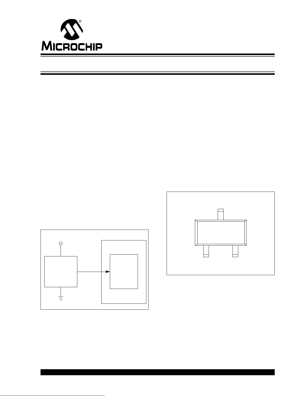
Block Diagram
= 2.5V to 5.5V
V
DD
PICmicro
Microcontroller
General Description
The TC1047 and TC1047A are linear voltage output
temperature sensors whose output voltage is directly
proportional to the measured temperature. The
TC1047 and TC1047A can accurately measure
temperatu re from -40°C to +125 °C. W ith the TC1047 ,
the supply voltage can vary between 2.7V and 4.4V.
The power supply range of the TC1047A is from 2.5V
to 5.5V.
The output voltage range for these devices is typically
100 mV at -40°C, 500 mV at 0°C, 7 50 mV at +25°C and
1.75V at +125°C. A 10 mV/°C voltage slope output
response allows for a predictable temperature
measurement over a wide temperature range. The
TC1047 and TC1047A are packaged in 3-pin SOT-23B
packages, making them ideal for space-critical
applications.
Package Type
3-Pin SOT-23B
TC1047/1047A
®
1
(NOTE)
V
SS
3
2
V
DD
TC1047A
V
SS
© 2005 Microchip Technology Inc. DS21498C-page 1
A/D
Converter
Note: 3-Pin SOT-23B is equivalent to JEDEC TO-236
V
DD
V
OUT
Page 2
TC1047/TC1047A
1.0 ELECTRICAL CHARACTERISTICS
Absolute Maximum Ratings*
Supply Voltage ......................................................+7V
Voltage on Any Pin with Respect to Supplies:
..................................................V
Operating Temperature ......................-40°C to +125°C
Storage Temperature Range..............-55°C to +150°C
ELECTRICAL CHARACTERISTICS
Electrical Specifications: Unless otherwise indicated,
and for T
Supply Voltage V
Supply Current, Operating I
Average Slope of Output Voltage A
Temperature Accuracy TMP
Output V oltage V
Output Source and Sink Current I
= -40°C to +125°C.
A
Parameters Sym Min Typ Max Units Conditions
-0.3 to VDD +0.3V
SS
DD
Q
V
ACY
OUT
1720 1750 1780 mV T
OUT
2.7 — 4.4 V TC1047
2.5 — 5.5 V TC1047A
—3560µA
— 10 — mV/°C
-2 ±0.5 +2 °C TA = 25°C
-3 ±0.5 +3 °C TA = +125°C
—1.0— °CT
—100— mVTA = -40°C
730 750 770 mV TA = 25°C
100 — — µA
*Stresses above those listed under "Absolute Maximum Ratings" may cause permanent damage to the device. These are
stress ratings only and functional operation of t he device at
these or any other conditions above those indicated in the
operation sections of the specifications is not implied. Exposure to Absolute Maximum Rating conditions for extended
periods may affect device reliability.
these specifications apply for the entire supply voltage range
= -40°C
A
= +125°C
A
TEMPERATURE CHARACTERISTICS
Electrical Specifications: Unless otherwise indicated, V
Parameters Sym Min Typ Max Units Conditions
Temperature Ranges
Specified Temperature Range T
Operating Temperatu re Ra nge T
Storage Temperature Range T
-40 — +85 °C
A
-40 — +125 °C Note 1
A
-65 — +150 °C
A
Thermal Package Resistances
Thermal Resistan ce , 3L -SO T-23B θ
—336 — °C/W
JA
Note 1: The TC1047/TC1047A operate over this extended temperature range, but with reduced performa nce . In
any case, the Junction Temperatur e (T
) must not exceed the Absolute Maximum specification of +150°C.
J
= +2.3V to +5.5V and VSS= GND.
DD
DS21498C-page 2 © 2005 Microchip Technology Inc.
Page 3
TC1047/TC1047A
5
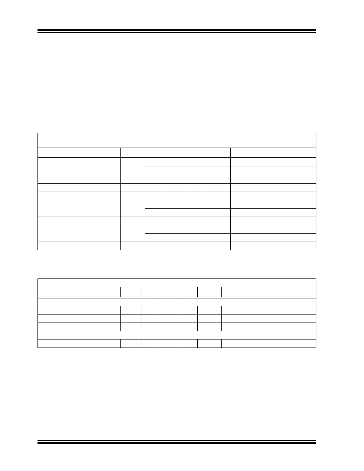
2.0 TYPICAL PERFORMANCE CURVES
Note: The graphs and tables provided following this note are a statistical summary b as ed on a limited number of
samples and are provided for informational purposes only. The performance characteristics listed herein
are not tested or guaranteed. In some graphs or tables, the data presented may be outside the specified
operating range (e.g., outside specified power supply range) and therefore outside the warranted range.
Note: Unless otherwise indicated, VDD = 2.7V thru 4.4V
3
2
1
0
Temp Accy (°C)
–1
–2
–3
–40
–25
5
20
35
50
–10
Temperature (°C)
65
VDD = 2.5V
=
5.5V
V
DD
80
95
110
125
FIGURE 2-1: Temperature Accuracy vs. Temperature.
and TA = -40°C to +125°C.
50
40
30
(μA)
DD
I
20
10
0
-40 -25 -10 5 20 35 50 65 80 95 110 12
VDD = 5.5V
VDD = 2.5V
Temp. (°C)
FIGURE 2-2: Supply Current vs. Temperature.
© 2005 Microchip Technology Inc. DS21498C-page 3
Page 4
TC1047/TC1047A
3.0 PIN DESCRIPTIONS
The descriptions of the pins are listed in Table 3-1.
TABLE 3-1: PIN FUNCTION TABLE
Pin No. Symbol Description
1V
2V
3V
DD
OUT
SS
4.0 DETAILED DESCRIPTION
The TC1047 and TC10 47A have an out put vol tage th at
varies linearly with temperature in degrees Celsius.
Figure 4-1 shows a plot of the output voltage versus
temperature for the TC1047 and TC1047A. The
temperature slope is fixed at 10 mV/°C and the output
voltage at 0°C is 500 mV.
V
Input Supp ly Voltage
Temperature Sensor Output Terminal
Ground Terminal
= (10 mV/°C) (Temperature °C) + 500 mV
OUT
1.75
1.7
1.5
1.3
1.1
(Volts)
0.9
OUT
V
0.7
0.5
0.3
0.1
–40
–30
–20 –10
0
10 20
30
40
T emperature (°C)
FIGURE 4-1: Output Voltage vs. Temperature.
50
60
70
80
90
100
110 120 125
DS21498C-page 4 © 2005 Microchip Technology Inc.
Page 5

5.0 PACKAGE INFORMATION
5.1 Package Marking Information
3-Pin SOT-23B
!"#$
1 & 2 = part number co de + temperature range a nd
voltage
Part Number Code
TC1047 AL
TC1047A BL
3 = year and quarter code
4 = lot ID number
TC1047/TC1047A
Legend: XX...X Customer-specific information*
Y Year code (last digit of calendar year)
YY Year code (last 2 digits of calendar year)
WW Week code (week of January 1 is week ‘01’)
NNN Alphanumeric traceability code
3
e
Pb-free JEDEC designator for Matte Tin (Sn)
* This package is Pb-free. The Pb-free JEDEC designator ( )
can be found on the outer packaging for this package.
Note: In the event the full Microchip part numb er cann ot be mark ed on one line, it wil l
be carried over to the next line, thus limiting the number of available
characters for customer-specific information.
© 2005 Microchip Technology Inc. DS21498C-page 5
3
e
Page 6

TC1047/TC1047A
3-Lead Plastic Small Outline Transistor (TT) (SOT-23)
E
E1
2
B
n
1
c
b
Number of Pins
Pitch
Outside lead pitch (basic)
Foot Angle
Lead Thickness
Mold Draft Angle Top
Mold Draft Angle Bottom
*Controll ing Parameter
Notes:
Dimensions D and E1 do not include mold flash or protrusions. Mold flash or protrusions shall not
exceed .005" (0.127mm) per side.
JEDEC Equivalent: TO-236
Drawing No. C04-104
n
p
p1
f
c
a
b
p1
D
p
A
f
L
A1
.038
a
A2
MILLIMETERSINCHES*Units
MAXNOMMINMAXNOMMINDimension Limits
33
0.96
1.92.076
1.121.010.89.044.040.035AOverall Height
1.020.950.88.040.037.035A2Molded Package Thickness
0.100.060.01.004.002.000A1Standoff
2.642.372.10.104.093.083EOverall Width
1.401.301.20.055.051.047E1Molded Package Width
3.042.922.80.120.115.110DOverall Length
0.550.450.35.022.018.014LFoot Length
10501050
0.180.140.09.007.006.004
0.510.440.37.020.017.015BLead Width
10501050
10501050
Revised 03-11-05
DS21498C-page 6 © 2005 Microchip Technology Inc.
Page 7

APPENDIX A: REVISION HISTORY
Revision C (May 2005)
The following is the list of modifications:
1. Added Appendix A: Revision History.
Revision B (May 2002)
Revision A (March 2001)
• Original Release of this Document.
TC1047/TC1047A
© 2005 Microchip Technology Inc. DS21498C-page 7
Page 8

TC1047/TC1047A
NOTES:
DS21498C-page 8 © 2005 Microchip Technology Inc.
Page 9

TC1047/TC1047A
PRODUCT IDENTIFICATION SYSTEM
To order or obtain information, e.g., on pricing or delivery, refer to the factory or the listed sales office.
PART NO. X
Device
Device: TC1047: Precision Temp-to-Voltage Converter
Temperature Range: V = -40°C to +125°C
Package: NB = Plastic Small Outline Transistor, SOT-23B, 3-lead
Temperature
Range
TC1047xTR: Precision Temp-to-Voltage Converter
XX
Package
(Tape and Reel)
Examples:
a) TC1047VNBTR: Precision Temp-to-Volt-
age Converter
b) TC1047AVNBTR: Precision Temp-to-Volt-
age Converter
© 2005 Microchip Technology Inc. DS21498C-page 9
Page 10

TC1047/TC1047A
NOTES:
DS21498C-page 10 © 2005 Microchip Technology Inc.
Page 11

Note the following details of the code protection feature on Microchip devices:
• Microchip products meet the specification contained in their particular Microchip Data Sheet.
• Microchip believes that i ts family of products is one of the most secure families of its kind on t he market today, when used in the
intended manner and under normal conditions.
• There are dishonest and possibly illegal methods used to breach the code protection feature. All of these methods, to our
knowledge, require using the Microchip products in a manner outside the operating specifications contained in Microchip’s Data
Sheets. Most likely, the person doing so is engaged in theft of intellectual property.
• Microchip is willing to work with the customer who is concerned about the integrity of their code.
• Neither Microchip nor any other semiconductor manufacturer can guarantee the security of their code. Code protection does not
mean that we are guaranteeing the product as “unbreakable.”
Code protection is constantly evolving. We at Microchip are com mitted to continuously improving the code protect ion f eatures of our
products. Attempts to break Microchip’s code protection feature may be a violation of the Digit al Mill ennium Copyright Act. If such acts
allow unauthorized access to your software or other copyrighted work, you may have a right to sue for relief under that Act.
Information contained in this publication regarding device
applications and the like is provided only for your convenience
and may be superseded by updates. It is your responsibility to
ensure that your application meets with your specifications.
MICROCHIP MAKES NO REPRESENTATIONS OR WARRANTIES OF ANY KIND WHETHER EXPRESS OR IMPLIED,
WRITTEN OR ORAL, STATUTORY OR OTHERWISE,
RELATED TO THE INFORMATION, INCLUDING BUT NOT
LIMITED TO ITS CONDITION, QUALITY, PERFORMANCE,
MERCHANTABILITY OR FITNESS FOR PURPOSE.
Microchip disclaims all liability arising from this information and
its use. Use of M icrochip’s prod ucts as critical components in
life support systems is not authorized except with express
written approval by Microchip. No licenses are conveyed,
implicitly or otherwise, under any Microchip intellectual property
rights.
Trademarks
The Microchip name and logo, the Microchip logo, Accuron,
dsPIC, K
EELOQ, microID, MPLAB, PIC, PICmicro,
PICSTART, PRO MATE, PowerSma rt , rfPIC, and
SmartShunt are registered trademarks of Microchip
Technology Incorporated in the U.S.A. and other countries.
AmpLab, FilterLab, Migratable Memory, MXDEV , MXLAB,
PICMASTER, SEEVAL, SmartSensor and The Embedded
Control Solutions Company are registered trademarks of
Microchip Technology Incorporated in the U.S.A.
Analog-for-the-Digital Age, Application Maestro, dsPICDEM,
dsPICDEM.net, dsPICworks, ECAN, ECONOMONITOR,
FanSense, FlexROM, fuzzyLAB, In-Circuit Serial
Programming, ICSP, ICEPIC, Linear Active Thermistor,
MPASM, MPLIB, MPLINK, MPSIM, PIC kit, PICDEM,
PICDEM.net, PICLAB, PICtail, PowerCal, PowerInfo,
PowerMate, PowerTool, rfLAB, rfPICDEM, Select Mode,
Smart Serial, SmartTel, Total Endurance and WiperLock are
trademarks of Microchip Technology Incorporated in the
U.S.A. and other countries.
SQTP is a service mark of Microchip T echnology Incorporated
in the U.S.A.
All other trademarks mentioned herein are property of their
respective companies.
© 2005, Microchip Technology Incorporated, Printed in the
U.S.A., All Rights Reserved.
Printed on recycled paper.
Microchip received ISO/TS-16949:2002 quality system certification for
its worldwide headquarters, design and wafer fabrication facilities in
Chandler and Tempe, Arizona and Mountain View, California in
October 2003. The Company’s quality system processes and
procedures are for its PICmicro
devices, Serial EEPROMs, microperipherals, nonvolatile memory and
analog products. In addition, Microchip’s quality system for the design
and manufacture of development systems is ISO 9001:2000 certified.
®
8-bit MCUs, KEELOQ
®
code hopping
© 2005 Microchip Technology Inc. DS21498C-page 11
Page 12

WORLDWIDE SALES AND SERVICE
AMERICAS
Corporate Office
2355 West Chandler Blvd.
Chandler, AZ 85224-6199
Tel: 480-792-7200
Fax: 480-792-7277
Technical Support:
http://support.microchip.com
Web Address:
www.microchip.com
Atlanta
Alpharetta, GA
Tel: 770-640-0034
Fax: 770-640-0307
Boston
Westborough, MA
Tel: 774-760-0087
Fax: 774-760-0088
Chicago
Itasca, IL
Tel: 630-285-0071
Fax: 630-285-0075
Dallas
Addison, TX
Tel: 972-818-7423
Fax: 972-818-2924
Detroit
Farmington Hills, MI
Tel: 248-538-2250
Fax: 248-538-2260
Kokomo
Kokomo, IN
Tel: 765-864-8360
Fax: 765-864-8387
Los Angeles
Mission Viejo, CA
Tel: 949-462-9523
Fax: 949-462-9608
San Jose
Mountain View, CA
Tel: 650-215-1444
Fax: 650-961-0286
Toronto
Mississauga, Ontario,
Canada
Tel: 905-673-0699
Fax: 905-673-6509
ASIA/PACIFIC
Australia - Sydney
Tel: 61-2-9868-6733
Fax: 61-2-9868-6755
China - Beijing
Tel: 86-10-8528-2100
Fax: 86-10-8528-2104
China - Chengdu
Tel: 86-28-8676-6200
Fax: 86-28-8676-6599
China - Fuzhou
Tel: 86-591-8750-3506
Fax: 86-591-8750-3521
China - Hong Kong SAR
Tel: 852-2401-1200
Fax: 852-2401-3431
China - Shanghai
Tel: 86-21-5407-5533
Fax: 86-21-5407-5066
China - Shenyang
Tel: 86-24-2334-2829
Fax: 86-24-2334-2393
China - Shenzhen
Tel: 86-755-8203-2660
Fax: 86-755-8203-1760
China - Shunde
Tel: 86-757-2839-5507
Fax: 86-757-2839-5571
China - Qingdao
Tel: 86-532-502-7355
Fax: 86-532-502-7205
ASIA/PACIFIC
India - Bangalore
Tel: 91-80-2229-0061
Fax: 91-80-2229-0062
India - New Delhi
Tel: 91-11-5160-8631
Fax: 91-11-5160-8632
Japan - Kanagawa
Tel: 81-45-471- 6166
Fax: 81-45-471-6122
Korea - Seoul
Tel: 82-2-554-7200
Fax: 82-2-558-5932 or
82-2-558-5934
Malaysia - Penang
Tel:011-604-646-8870
Fax:011-604-646-5086
Philippines - Manila
Tel: 011-632-634-9065
Fax: 011-632-634-9069
Singapore
Tel: 65-6334-8870
Fax: 65-6334-8850
Taiwan - Kaohsiung
Tel: 886-7-536-4818
Fax: 886-7-536-4803
Taiwan - Taipei
Tel: 886-2-2500-6610
Fax: 886-2-2508-0102
Taiwan - Hsinchu
Tel: 886-3-572-9526
Fax: 886-3-572-6459
EUROPE
Austria - Weis
Tel: 43-7242-2244-399
Fax: 43-7242-2244-393
Denmark - Ballerup
Tel: 45-4450-2828
Fax: 45-4485-2829
France - Massy
Tel: 33-1-69-53-63-20
Fax: 33-1-69-30-90-79
Germany - Ismaning
Tel: 49-89-627-144-0
Fax: 49-89-627-144-44
Italy - Milan
Tel: 39-0331-742611
Fax: 39-0331-466781
Netherlands - Drunen
Tel: 31-416-690399
Fax: 31-416-690340
England - Berkshire
Tel: 44-118-921-5869
Fax: 44-118-921-5820
04/20/05
DS21498C-page 12 © 2005 Microchip Technology Inc.
 Loading...